

Page 1
STR-DE898/DE998
SERVICE MANUAL
Ver. 1.0 2005. 04
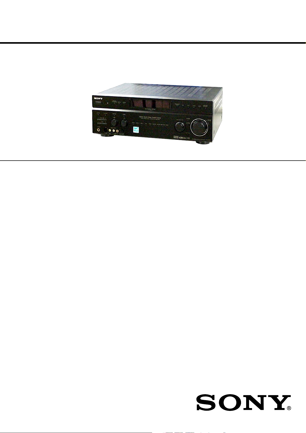
Photo: STR-DE998
Manufactured under license from Dolby Laboratories.
“Dolby”, “Pro Logic” and the double-D symbol are
trademarks of Dolby Laboratories.
“DTS”, “DTS-ES”, “Neo:6” and “DTS 96/24” are
trademarks of Digital Theater Systems, Inc.
SPECIFICATIONS
US Model
Canadian Model
STR-DE898/DE998
E Model
Australian Model
STR-DE898
AUDIO POWER SPECIFICATIONS
POWER OUTPUT AND TOTAL HARMONIC
DISTORTION:
(Models of area code US only)
With 8 ohm loads, both channels driven, from
20 – 20,000 Hz; rated 100 watts (STR-DE898)/
110 watts (STR-DE998) per channel minimum
RMS power, with no more than 0.09 % total
harmonic distortion from 250 milliwatts to
rated output.
Amplifier section
Power Output
Models of area code STR-DE898: US, CND
Rated Power Output at Stereo Mode
(8 ohms 20 Hz – 20 kHz, THD 0.09 %)
(8 ohms 1 kHz, THD 0.7 %)
(8 ohms 1 kHz, THD 10 %)
Reference Power Output
(8 ohms 20 Hz – 20 kHz, THD 0.09 %)
(8 ohms 1 kHz, THD 0.7 %)
(8 ohms 1 kHz, THD 10 %)
100 W + 100 W
110 W + 110 W
140 W + 140 W
1)
FRONT
CENTER
SURR
SURR BACK
FRONT
CENTER
SURR
SURR BACK
FRONT
CENTER
SURR
SURR BACK
2)
: 100 W/ch
2)
: 100 W
2)
: 100 W/ch
2)
: 110 W/ch
2)
: 110 W
2)
: 110 W/ch
2)
: 140 W/ch
2)
: 140 W
2)
: 140 W/ch
1)
1)
1)
2)
: 100 W/ch
2)
: 110 W/ch
2)
: 140 W/ch
Models of area code E2
Rated Power Output at Stereo Mode
(8 ohms 20 Hz – 20 kHz, THD 0.09 %)
(8 ohms 1 kHz, THD 0.7 %)
(8 ohms 1 kHz, THD 10 %)
Reference Power Output
(8 ohms 20 Hz – 20 kHz, THD 0.09 %)
(8 ohms 1 kHz, THD 0.7 %)
(8 ohms 1 kHz, THD 10 %)
90 W + 90 W
100 W + 100 W
125 W + 125 W
1)
FRONT
CENTER
SURR
SURR BACK
FRONT
CENTER
SURR
SURR BACK
FRONT
CENTER
SURR
SURR BACK
2)
: 115 W/ch
2)
: 115 W
2)
: 115 W/ch
2)
: 125 W/ch
2)
: 125 W
2)
: 125 W/ch
2)
: 155 W/ch
2)
: 155 W
2)
: 155 W/ch
1)
1)
1)
2)
: 115 W/ch
2)
: 125 W/ch
2)
: 155 W/ch
– Continued on next page –
FM STEREO/FM-AM RECEIVER
9-879-624-01
2005D0479-1
© 2005. 04
Sony Corporation
Audio Group
Published by Sony Engineering Corporation
1
Page 2

STR-DE898/DE998
Models of area code AR
Rated Power Output at Stereo Mode
(8 ohms 20 Hz – 20 kHz, THD 0.09 %)
90 W + 90 W
80 W + 80 W
(8 ohms 1 kHz, THD 0.7 %)
100 W + 100 W
95 W + 95 W
(8 ohms 1 kHz, THD 10 %)
130 W + 130 W
120 W + 120 W
Reference Power Output
1)
(8 ohms 20 Hz – 20 kHz, THD 0.09 %)
FRONT
CENTER
SURR
SURR BACK
(8 ohms 1 kHz, THD 0.7 %)
FRONT
CENTER
SURR
SURR BACK
(8 ohms 1 kHz, THD 10 %)
FRONT
CENTER
SURR
SURR BACK
2)
: 115 W/ch
2)
: 115 W
2)
: 115 W/ch
2)
: 125 W/ch
2)
: 125 W
2)
: 125 W/ch
2)
: 155 W/ch
2)
: 155 W
2)
: 155 W/ch
1)
3)
1)
3)
1)
3)
2)
: 115 W/ch
2)
: 125 W/ch
2)
: 155 W/ch
Models of area code STR-DE998: US, CND
Rated Power Output at Stereo Mode
(8 ohms 20 Hz – 20 kHz, THD 0.09 %)
110 W + 110 W
(8 ohms 1 kHz, THD 0.7 %)
120 W + 120 W
(8 ohms 1 kHz, THD 10 %)
150 W + 150 W
Reference Power Output
1)
(8 ohms 20 Hz – 20 kHz, THD 0.09 %)
FRONT
CENTER
SURR
SURR BACK
(8 ohms 1 kHz, THD 0.7 %)
FRONT
CENTER
SURR
SURR BACK
(8 ohms 1 kHz, THD 10 %)
FRONT
CENTER
SURR
SURR BACK
2)
: 110 W/ch
2)
: 110 W
2)
: 110 W/ch
2)
: 120 W/ch
2)
: 120 W
2)
: 120 W/ch
2)
: 150 W/ch
2)
: 150 W
2)
: 150 W/ch
1)
1)
1)
2)
: 110 W/ch
2)
: 120 W/ch
2)
: 150 W/ch
1) Measured under the following conditions:
Area code Power requirements
US, CND 120 V AC, 60 Hz
E2 240 V AC, 50 Hz
AR 230 V AC, 50 Hz
2) Depending on the sound field settings and the
source, there may be no sound output.
3) Measured under the following conditions:
Area code Power requirements
AR 220 V AC, 50 Hz
Frequency response
PHONO RIAA equalization curve
±0.5 dB
MULTI CH IN, 10 Hz – 70 kHz
SA-CD/CD, TV/SAT, +0.5/–2 dB (with sound
MD/TAPE, DVD, field and equalizer
VIDEO 1, 2, 3 bypassed)
Inputs (Analog)
PHONO Sensitivity: 8 mV
Impedance: 50 k ohms
4)
S/N
: 86 dB
5)
(A, 8 mV
)
MULTI CH IN, Sensitivity: 500 mV
SA-CD/CD, TV/SAT, Impedance: 50 k ohms
MD/TAPE, DVD, S/N
VIDEO 1, 2, 3 (A, 500 mV
4)
: 96 dB
5)
)
4) INPUT SHORT (with sound field and equalizer
bypassed).
5) Weighted network, input level.
Inputs (Digital)
DVD, SA-CD/CD Sensitivity: –
(Coaxial) Impedance: 75 ohms
S/N: 100 dB
(A, 20 kHz LPF)
TV/SAT, SA-CD/CD, Sensitivity: –
MD/TAPE, VIDEO 3 Impedance: –
(Optical) S/N: 100 dB
(A, 20 kHz LPF)
Outputs (Analog)
MD/TAPE (OUT), Voltage: 500 mV
VIDEO 1, 2 Impedance: 10 k ohms
(AUDIO OUT)
SUB WOOFER Voltage: 2 V
Impedance: 1 k ohm
Outputs (Digital)
MD/TAPE (Optical) Sensitivity: –
Equalizer
Gain levels ±10 dB, 0.5 dB step
FM tuner section
Tuning range 87.5 – 108.0 MHz
Antenna FM wire antenna
Antenna terminals 75 ohms, unbalanced
Intermediate frequency 10.7 MHz
Sensitivity
Mono: 18.3 dBf, 2.2 µV/75 ohms
Stereo: 38.3 dBf, 22.5 µV/75 ohms
Useable sensitivity 11.2 dBf, 1 µV/75 ohms
S/N
Mono: 76 dB
Stereo: 70 dB
Harmonic distortion at 1 kHz
Mono: 0.3%
Stereo: 0.5%
Separation 45 dB at 1 kHz
Frequency response 30 Hz – 15 kHz,
+0.5/–2 dB
Selectivity 60 dB at 400 kHz
AM tuner section
Tuning range
Models of area code US, CND
With 10-kHz tuning scale: 530 – 1,710 kHz
With 9-kHz tuning scale: 531 – 1,710 kHz
Models of area code E2
With 10-kHz tuning scale: 530 – 1,610 kHz
With 9-kHz tuning scale: 531 – 1,602 kHz
6)
6)
6)
6)
Models of area code AR
With 10-kHz tuning scale: 530 – 1,610 kHz
Antenna Loop antenna
Intermediate frequency 450 kHz
Usable sensitivity 50 dB/m (at 1,000 kHz or
999 kHz)
S/N 54 dB (at 50 mV/m)
Harmonic distortion 0.5 % (50 mV/m, 400 Hz)
Selectivity
At 9 kHz: 35 dB
At 10 kHz: 40 dB
6) You can change the AM tuning scale to 9 kHz or 10 kHz.
After tuning in any AM station, turn off the receiver. While
holding down PRESET TUNING + or TUNING +, press
?/1. All preset stations will be erased when you change
the tuning scale. To reset the scale to 10 kHz (or 9 kHz),
repeat the procedure.
Video section
Inputs/Outputs
Video: 1 Vp-p, 75 ohms
S-video: Y: 1 Vp-p, 75 ohms
COMPONENT VIDEO: Y: 1 Vp-p, 75 ohms
80 MHz HD Pass Through
C: 0.286 Vp-p, 75 ohms
PB/CB/B-Y: 0.7 Vp-p,
75 ohms
PR/CR/R-Y: 0.7 Vp-p,
75 ohms
2
Page 3
STR-DE898/DE998
1.5 k
Ω
0.15 µF
AC
voltmeter
(0.75 V)
To Exposed Metal
Parts on Set
Earth Ground
General
Power requirements
Area code Power requirements
US, CND 120 V AC, 60 Hz
E2 120/220/240 V AC,
50/60 Hz
AR 220 – 230 V AC, 50/60 Hz
Power consumption
Area code Power consumption
US, E2 300 W
CND 410 VA
AR 270 W
Power consumption (during standby mode)
0.3 W
AC outlets
(Except for models of area code AR)
Area code AC outlets
US, CND 2 switched,
120 W/1A MAX
E2 1 switched, 100 W MAX
Dimensions (w/h/d) (Approx.)
STR-DE898: 430 × 157.5 × 371 mm
(16 7/8 × 6 2/8 × 14 5/8
inches) including
projecting parts and
controls
STR-DE998: 430 × 157.5 × 402 mm
(16 7/8 × 6 2/8 × 15 7/8
inches) including
projecting parts and
controls
Mass (Approx.)
STR-DE898: 10.5 kg (23 lb 3 oz)
STR-DE998: 13.5 kg (29 lb 13 oz)
SAFETY CHECK-OUT (US MODEL)
After correcting the original service problem, perform the following safety check before releasing the set to the customer:
Check the antenna terminals, metal trim, “metallized” knobs, screws,
and all other exposed metal parts for AC leakage.
Check leakage as described below.
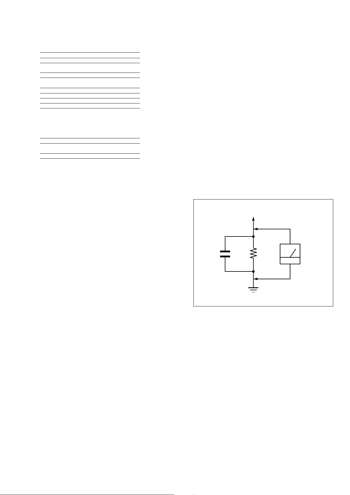
LEAKAGE TEST
The AC leakage from any exposed metal part to earth ground and
from all exposed metal parts to any exposed metal part having a
return to chassis, must not exceed 0.5 mA (500 microampers.).
Leakage current can be measured by any one of three methods.
1. A commercial leakage tester, such as the Simpson 229 or RCA
WT-540A. Follow the manufacturers’ instructions to use these
instruments.
2. A battery-operated AC milliammeter. The Data Precision 245
digital multimeter is suitable for this job.
3. Measuring the voltage drop across a resistor by means of a
VOM or battery-operated AC voltmeter. The “limit” indication is 0.75 V, so analog meters must have an accurate lowvoltage scale. The Simpson 250 and Sanwa SH-63Trd are examples of a passive VOM that is suitable. Nearly all battery
operated digital multimeters that have a 2 V AC range are suitable. (See Fig. A)
Supplied accessories
FM wire antenna (1)
AM loop antenna (1)
Remote commander RM-AAL001 (1)
(STR-DE898: US, CND, E2, AR)
Remote commander RM-AAE001 (1) (STR-DE998)
Remote commander RM-AAP002 (1)
(STR-DE898: AUS, SP, MY)
R6 (size-AA) batteries (2)
Design and specifications are subject to change
without notice.
•Abbreviation
CND : Canadian model
E2 : AC 120 V area in E model
AR : Argentina model
AUS: Australian model
SP : Singapore model
MY : Malaysia model
SAFETY-RELATED COMPONENT WARNING!!
COMPONENTS IDENTIFIED BY MARK 0 OR DOTTED LINE
WITH MARK 0 ON THE SCHEMATIC DIAGRAMS AND IN
THE PARTS LIST ARE CRITICAL TO SAFE OPERATION.
REPLACE THESE COMPONENTS WITH SONY PARTS WHOSE
PART NUMBERS APPEAR AS SHOWN IN THIS MANUAL OR
IN SUPPLEMENTS PUBLISHED BY SONY.
Fig. A. Using an AC voltmeter to check AC leakage.
ATTENTION AU COMPOSANT AYANT RAPPORT
À LA SÉCURITÉ!!
LES COMPOSANTS IDENTIFIÉS PAR UNE MARQUE 0 SUR LES
DIAGRAMMES SCHÉMATIQUES ET LA LISTE DES PIÈCES
SONT CRITIQUES POUR LA SÉCURITÉ DE FONCTIONNEMENT.
NE REMPLACER CES COMPOSANTS QUE PAR DES PIÈCES
SONY DONT LES NUMÉROS SONT DONNÉS DANS CE MANUEL
OU DANS LES SUPPLÉMENTS PUBLIÉS PAR SONY.
3
Page 4
STR-DE898/DE998
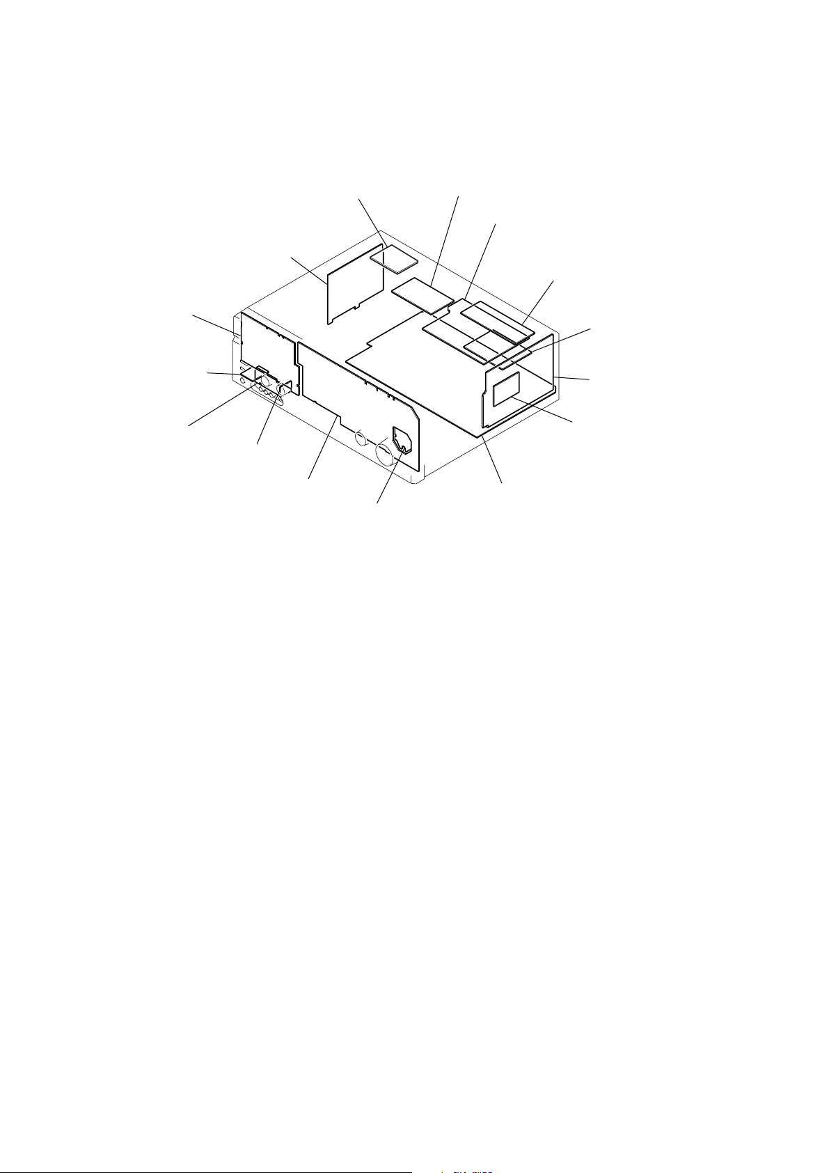
MODEL IDENTIFICATION
— BACK PANEL —
Par t No.
MODEL PART No.
STR-DE898: US 2-514-879-0s
STR-DE898: CND 2-514-879-1s
STR-DE898: SP, MY 2-514-879-2s
STR-DE898: AUS 2-514-879-3s
STR-DE898: E2 2-514-879-4s
STR-DE898: AR 2-514-879-5s
STR-DE998: US 2-580-905-0s
STR-DE998: CND 2-580-905-1s
•Abbreviation
CND: Canadian model
SP : Singapore model
MY : Malaysia model
AUS: Australian model
E2 : AC 120 V area in E model
AR : Argentina model
TABLE OF CONTENTS
1. GENERAL
Main Unit (STR-DE898) .........................................................5
Remote Button Description
(STR-DE898: US, CND, E2, AR model) ................................ 6
Main Unit (STR-DE998) .........................................................7
Remote Button Description (STR-DE998) ............................. 8
2. DISASSEMBLY
2-1. Case ....................................................................................... 9
2-2. Front Panel Section ............................................................. 10
2-3. Back Panel Section.............................................................. 10
2-4. Digital Board ....................................................................... 11
2-5. Main Board ......................................................................... 11
2-6. STBY Board ........................................................................ 12
3. TEST MODE ............................................................... 13
4. DIAGRAMS
4-1. Circuit Boards Location ...................................................... 14
4-2. Block Diagram — Tuner/Audio Section —........................ 15
4-3. Block Diagram — Digital Section — ................................. 16
4-4. Block Diagram — Video Section — ................................... 17
4-5. Block Diagram — Key/Display Section — ........................ 18
4-6. Block Diagram — OSD Section — .................................... 19
4-7. Block Diagram — Power Section — .................................. 20
4-8. Printed Wiring Boards — Main Section — ........................ 22
4-9. Schematic Diagram — Main Section (1/3) — .................... 23
4-10. Schematic Diagram — Main Section (2/3) — .................. 24
4-11. Schematic Diagram — Main Section (3/3) — .................. 25
4-12. Printed Wiring Board — Digital Section (Side A) — ....... 26
4-13. Printed Wiring Board — Digital Section (Side B) —....... 27
4-14. Schematic Diagram — Digital Section (1/5) — ............... 28
4-15. Schematic Diagram — Digital Section (2/5) — ............... 29
4-16. Schematic Diagram — Digital Section (3/5) — ............... 30
4-17. Schematic Diagram — Digital Section (4/5) — ............... 31
4-18. Schematic Diagram — Digital Section (5/5) — ............... 32
4-19. Printed Wiring Boards — AV SYNC JRC Section — ...... 33
4-20. Schematic Diagram — AV SYNC JRC Section — .......... 33
4-21. Printed Wiring Board — Speaker Section — ................... 34
4-22. Schematic Diagram — Speaker Section — ...................... 34
4-23. Printed Wiring Boards — Video (AU) Section — ........... 35
4-24. Schematic Diagram — Video (AU) Section —................. 36
4-25. Printed Wiring Board — Video Section (Side A) —......... 37
4-26. Printed Wiring Board — Video Section (Side B) —......... 38
4-27. Schematic Diagram — Video Section (1/2) — ................. 39
4-28. Schematic Diagram — Video Section (2/2) — ................. 40
4-29. Printed Wiring Board — S-video Section —.................... 41
4-30. Schematic Diagram — S-video Section — ....................... 41
4-31. Printed Wiring Boards — Display Section— ................... 42
4-32. Schematic Diagram — Display Section—........................ 43
4-33. Printed Wiring Boards — STBY Section —..................... 44
4-34. Schematic Diagram — STBY Section — ......................... 45
5. EXPLODED VIEWS
5-1. Case Section ........................................................................ 58
5-2. Front Panel Section ............................................................. 59
5-3. Back Panel Section.............................................................. 60
5-4. Chassis Section ................................................................... 61
6. ELECTRICAL PARTS LIST..................................... 62
4
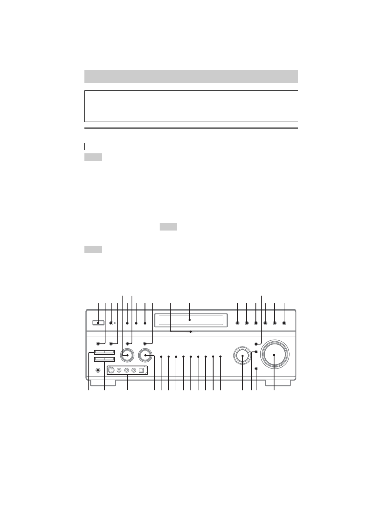
Page 5
SECTION 1
Illustrati
GENERAL
STR-DE898:
List of button locations and reference pages
STR-DE898/DE998
This section is extracted
from instruction manual.
How to use this page
Use this page to find the location of buttons and other
parts of the system that are mentioned in the text.
Main unit
ALPHABETICAL ORDER
A - L
A.F.D. (button/indicator) qf (30,
33)
DIMMER 8 (26)
DISPLAY 7 (26, 58)
Display q; (26)
DVD (indicator) wj (23)
ENTER 9 (17, 18, 41, 59)
FM MODE 4 (24)
INPUT MODE w; (36)
INPUT SELECTOR wa (23, 24,
25, 26, 36, 40, 41, 58)
IR (receptor) 3 (45, 59)
M - O
MAIN MENU 5 (18, 37, 38, 41)
MASTER VOLUME –/+ qk (17,
22, 23, 57)
MD/TAPE (indicator) wg (23)
MEMORY 2 (25)
MOVIE (button/indicator) qg
(31, 32, 58)
MULTI CHANNEL DECODING
(indicator) qa (24)
MULTI CH IN/DIRECT qs (24,
29)
MUSIC (button/indicator) qh (32,
58)
P - Z
PHONES (jack) eg (23, 57)
PHONO (indicator) ws (23)
PRESET TUNING +/– eh (25,
61)
SA-CD/CD (indicator) wf (23)
SPEAKERS (OFF/A/B/A+B) 6
(16, 42, 57)
on number
r
DISPLAY 7 (26, 58)
Name of button/part Reference page
RR
SURR BACK DECODING qj
(33)
TUNER FM/AM (indicator) wd
(23)
TUNING +/– ef (24, 61)
TV/SAT (indicator) wh (23)
VIDEO 1 (indicator) e; (23)
VIDEO 2 (indicator) wl (23)
VIDEO 3 (indicator) wk (23)
VIDEO 3 IN/PORTABLE AV IN
(jacks) ed (13)
NUMBERS AND SYMBOLS
2CH (button/indicator) qd (29,
33, 38)
2ND ZONE ql (43)
–/+ ea (18, 37, 38, 41)
?/1 (power) 1 (17, 18, 22, 38,
59, 61)
</> es (18, 37, 38, 41)
2156734
8 9 q; qa qs qfqd qg qh qj
edegeh ef
eaes
wswdwfwgwhwjwkwle;
wa
ql qk
w;
5
Page 6
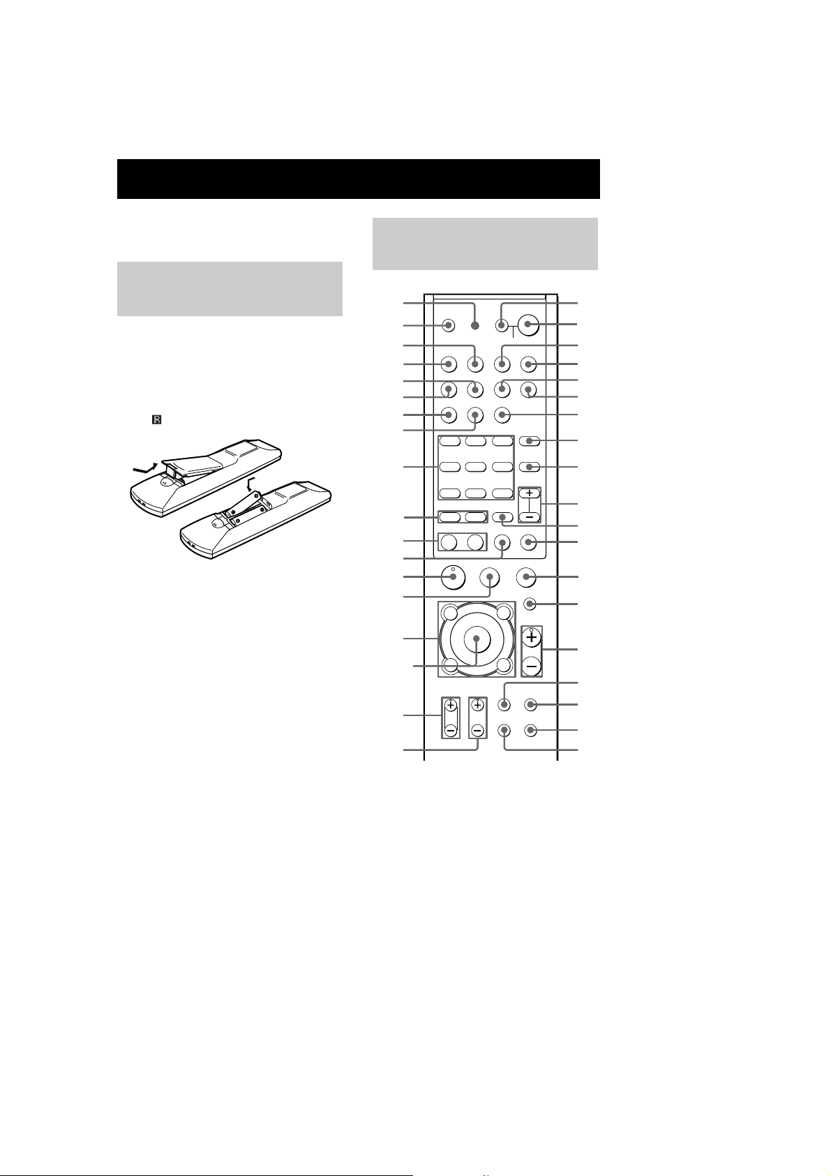
STR-DE898/DE998
STR-DE898: US, CND, E2, AR model
Operations Using the Remote RM-AAL001
You can use the remote RM-AAL001 to operate
the components in your system.
Before you use your
Remote button
description
remote
Inserting batteries into the
remote
Insert R6 (size-AA) batteries with the + and –
properly oriented in the battery compartment.
When using the remote, point it at the remote
sensor on the receiver.
Tip
Under normal conditions, the batteries should last for
about 6 months. When the remote no longer operates
the receiver, replace all batteries with new ones.
Notes
•Do not leave the remote in an extremely hot or hum id
place.
•Do not use a new battery with an old one.
•Do not expose the remote sensor to direct sunlight or
lighting apparatuses. Doing so may cause a
malfunction.
•If you do not use the remote for an extended period
of time, remove the batteries to avoid possible
damage from battery leakage and corrosion.
eh
eg
ef
ed
es
ea
e;
wl
wk
wj
wh
wg
*
wf
wd
ws
ENTER
*
wa
TV ?/1 AV ?/1
RM SET UP
SYSTEM STANDBY
VIDEO1 VIDEO2
AV1 AV2 2ND
MD/TAPE SA-CD/CD
TV/SAT
M1 M2
MULTI CH SOURCE
PHONO
2CH
A.F.D.
123
TEST
TONE
456
ANGLE
AUDIO
789
SUBTITLE ENTER
>
.
0/10 >10/11 12
SHIFT
D.TUNING DISC ALT
M
m
ANT
CLEAR
SEARCH MODE
X
H
TOP MENU/
GUIDE
F
G
f
DISPLAY
TV VOL TV CH
RETURN/EXIT
?/1
PL
SLEEP
VIDEO3 DVD
TUNER
MOVIE
MUSIC
DUAL
MONO
DECODINGDIRECT
JUMP/
PRESET/
TIME
CH/D.SKIP
-
x
MUTING
AV MENU
MASTER
g
O
TV/
MAIN
VIDEO
MENU
WIDE DIMMER
SB
VOL
1
2
3
4
5
6
7
8
9
q;
qa
qs
qd
qf
qg
qh
qj
qk
*
w;
*The H, TV VOL +, TV CH + and MASTER VOL
+ buttons have a tactile dot. Use the tactile dot as a
reference when operating the receiver and other
audio/video components.
ql
*
6
Page 7
STR-DE998:
Illustrati
List of button locations and reference pages
STR-DE898/DE998
How to use this page
Use this page to find the location of buttons and other
parts of the system that are mentioned in the text.
Main unit
ALPHABETICAL ORDER
A - I
A.F.D. (button/indicator) qg (30,
33)
DIMMER 9 (26)
DISPLAY 8 (26, 58)
Display qs (27)
DVD (indicator) wl (23)
ENTER q; (17, 41, 59)
FM MODE 4 (24)
INPUT MODE wa (36)
INPUT SELECTOR wd (23, 24,
25, 36, 40, 41, 58)
IR (receptor) 3 (45, 59)
M - O
MAIN MENU 7 (18, 37, 38, 41)
MASTER VOLUME –/+ w; (22,
23, 57)
MD/TAPE (indicator) wj (23)
MEMORY 2 (25)
MENU 5 (18, 37, 38, 41)
MOVIE (button/indicator) qj
(31, 32, 58)
MULTI CHANNEL DECODING
(indicator) qa (24)
MULTI CH IN/DIRECT qd (24,
29)
MUSIC (button/indicator) qk ( 32,
58)
ON SCREEN ws (13)
P - Z
PHONES (jack) eh (23, 57)
PHONO (indicator) wf (23)
PRESET TUNING +/– ej (25,
61)
SA-CD/CD (indicator) wh (23)
on number
r
DISPLAY 8 (26, 58)
Name of button/part Reference page
RR
SPEAKERS (OFF/A/B/A+B) 6
(16, 42, 57)
SURR BACK DECODING ql
(33)
TUNER FM/AM (indicator) wg
(23)
TUNING +/– eg (24, 61)
TV/SAT (indicator) wk (23)
VIDEO 1 (indicator) es (23)
VIDEO 2 (indicator) ea (23)
VIDEO 3 (indicator) e; (23)
VIDEO 3 IN/PORTABLE AV IN
(jacks) ef (13)
NUMBERS AND SYMBOLS
2CH (button/indicator) qf (29,
33, 38)
2ND ZONE qh (43)
?/1 (power) 1 (17, 18, 22, 38,
59, 61)
–/+ ed (18, 37, 38, 41)
2
1
ehej eg
57 qh
6834
9 q; qsqa qd qgqf qj qk ql
edef
wd wswfwgwhwjwkwle;eaes
wa
w;
7
Page 8
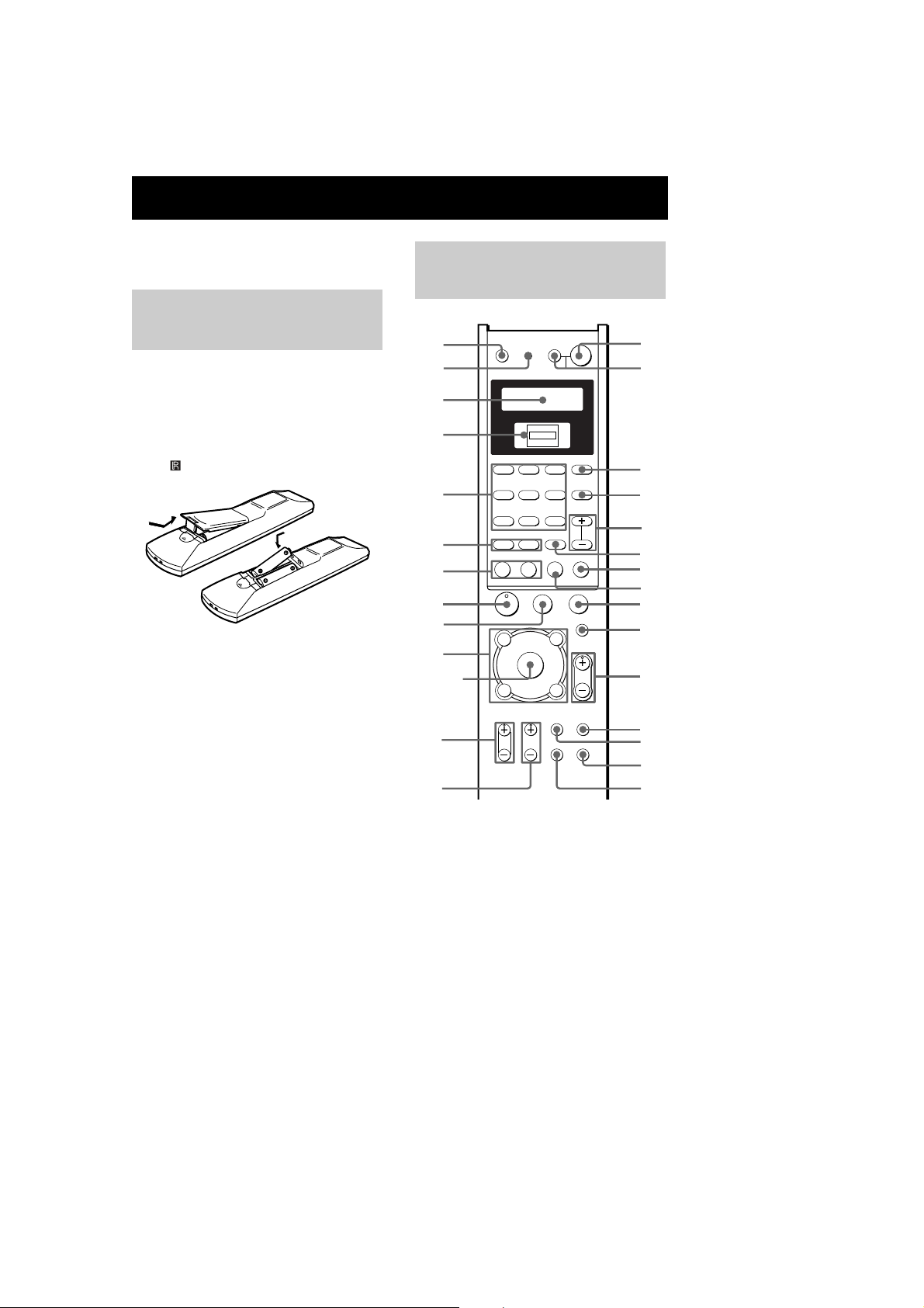
STR-DE898/DE998
STR-DE998:
Operations Using the Remote RM-AAE001
You can use the remote RM-AAE001 to operate
the components in your system.
Before you use your
Remote button
description
remote
Inserting batteries into the
remote
Insert R6 (size-AA) batteries with the + and –
properly oriented in the battery compartment.
When using the remote, point it at the remote
sensor on the receiver.
Tip
Under normal conditions, the batteries should last for
about 6 months. When the remote no longer operates
the receiver, replace all batteries with new ones.
Notes
•Do not leave the remote in an extremely hot or hum id
place.
•Do not use a new battery with an old one.
•Do not expose the remote sensor to direct sunlight or
lighting apparatuses. Doing so may cause a
malfunction.
•If you do not use the remote for an extended period
of time, remove the batteries to avoid possible
damage from battery leakage and corrosion.
1
2
TV ?/1 AV ?/1
RM SET UP
SYSTEM STANDBY
?/1
PL
SLEEP
wj
wh
3
v
4
5
6
7
*
8
9
0
ENTER
*
qa
TOP MENU/
PUSH
2CH
A.F.D.
123
TEST
TONE
456
SWAP/
AUDIO
ANGLE
789
SUBTITLE ENTER
>
.
0/10 >10/11 12
SHIFT
D.TUNING DISC ALT
M
m
ANT
CLEAR
H
GUIDE
F
G
f
DISPLAY
RETURN/EXIT
TV VOL TV CH
V
MOVIE
DUAL
MONO
JUMP/
TIME
-
SEARCH MODE
X
AV MENU
g
O
TV/
VIDEO
WIDE ON SCREEN
MUSIC
SB
DECODINGDIRECT
PRESET/
CH/D.SKIP
x
MUTING
MASTER
VOL
MAIN
MENU
wg
wf
wd
ws
wa
w;
ql
qk
qj
qh
qg
qf
*
qs
*The H, TV VOL +, TV CH + and MASTER VOL
+ buttons have a tactile dot. Use the tactile dot as a
reference when operating the receiver and other
audio/video components.
qd
*
8
Page 9
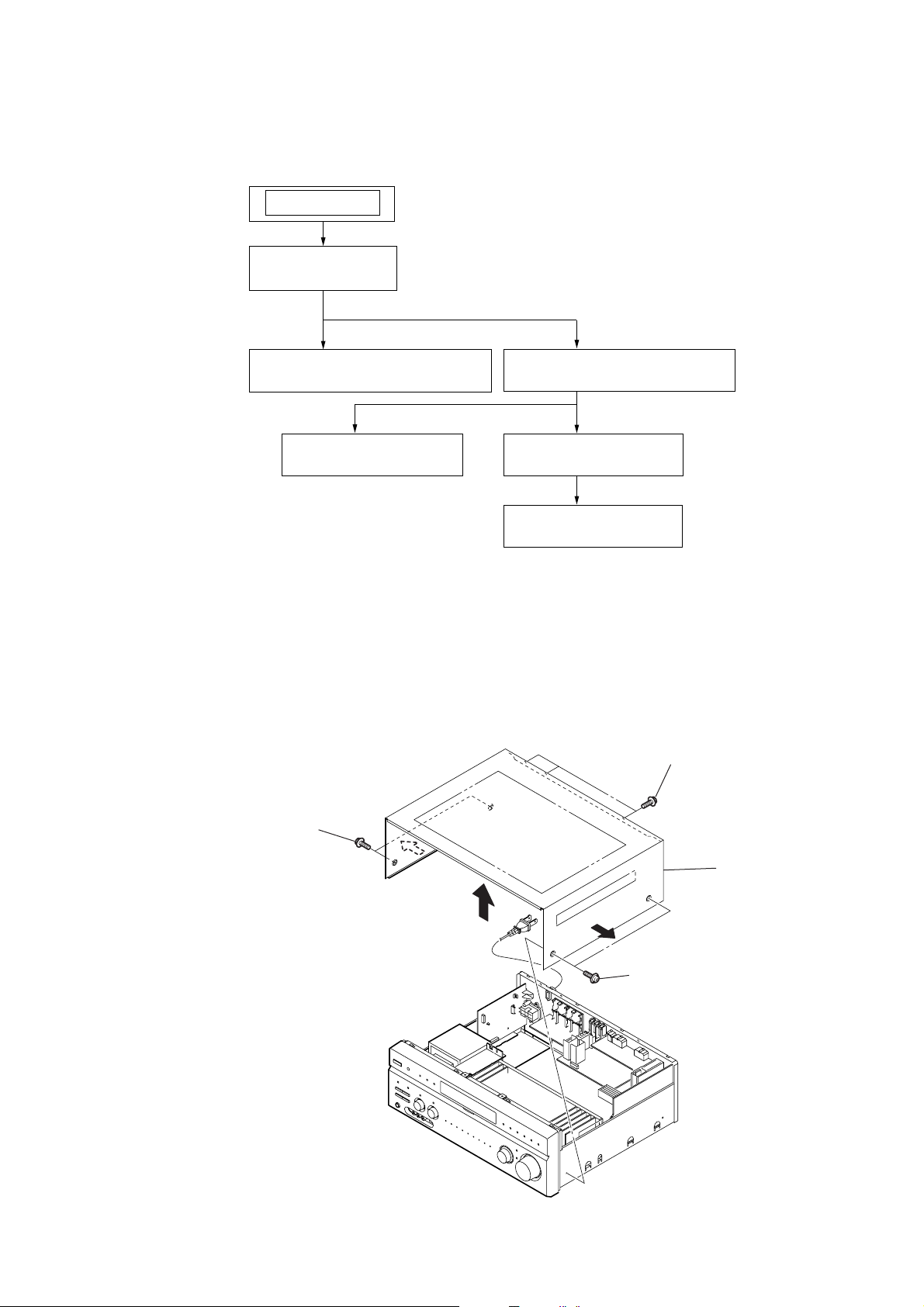
SECTION 2
DISASSEMBLY
Note : This set can be disassemble according to the following sequence.
SET
2-1. CASE
(Page 9)
STR-DE898/DE998
2-2. FRONT PANEL SECTION
2-3. BACK PANEL SECTION
(Page 10)
2-6. STBY BOARD
2-4. DIGITAL BOARD
(Page 12)
2-5. MAIN BOARD
Note : Follow the disassembly procedure in the numerical order given.
2-1. CASE
(Page 10)
(Page 11)
(Page 11)
2
three screws
(case 3 TP2)
1
two screws
(case 3 TP2)
3
two screws
(case 3 TP2)
4
case
9
Page 10
STR-DE898/DE998
)
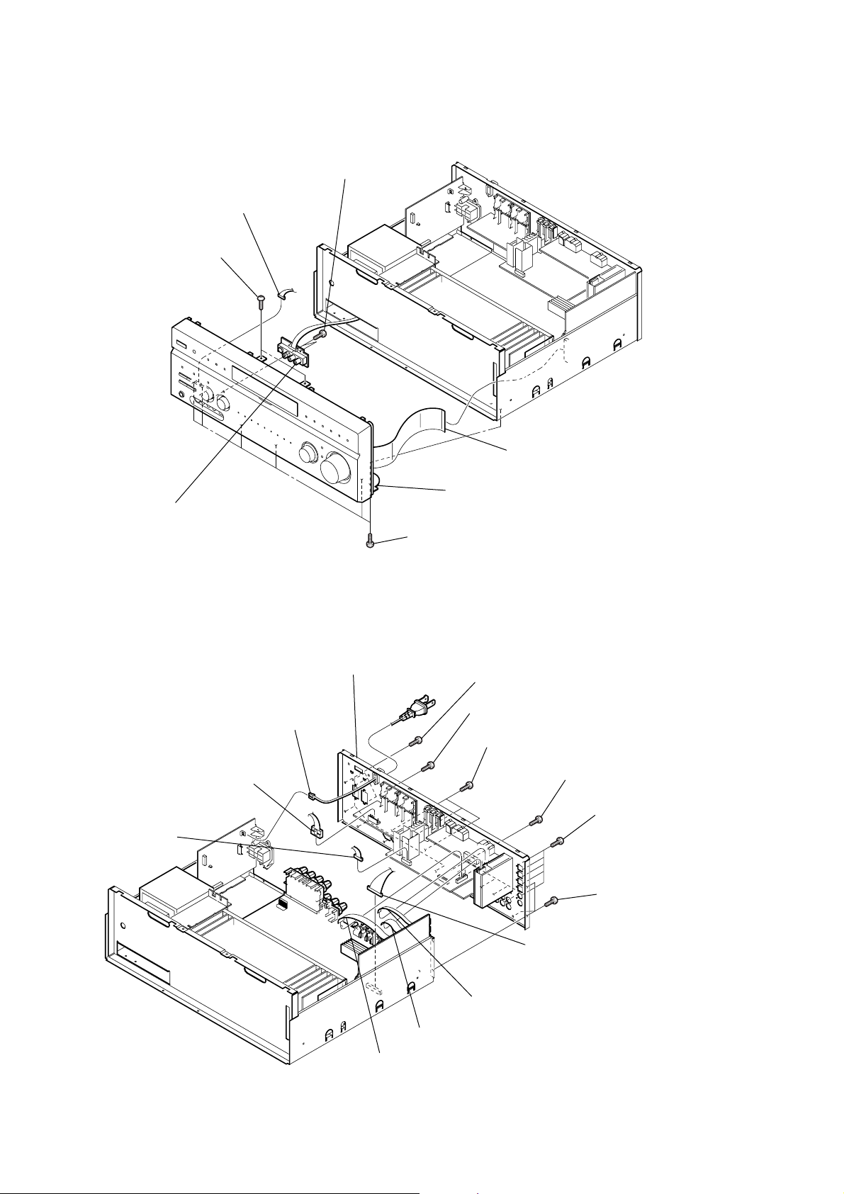
2-2. FRONT PANEL SECTION
2
two screws
(+BVTP 3
×
8)
4
CNP701 (4P)
5
two screws
(+BVTP 3
×
8)
6
V3 board (DE898)
FRONT AV board (DE998)
2-3. BACK PANEL SECTION
5
6
CNP207
CNP851
4
CNP901
3
six screws
qf
back panel section
7
front panel section
(+BVTP 3
9
0
1
CNS505
×
8)
five screws
(+BVTP 3
three screws
(+BVTP 3
qa
three screws
(+BVTP 3
×
8)
×
8)
×
8)
qs
five screws
(+BVTP 3
qd
five screws
(+BVTP 3
×
8)
×
8)
10
3
CNP210
2
connector
1
CNS204
7
CNP812
8
three screws
(+BVTP 3
×
8
Page 11
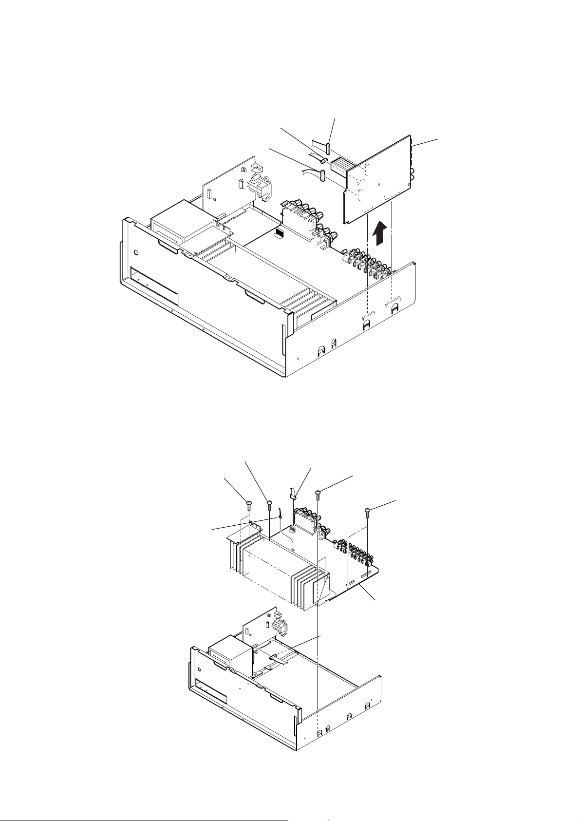
2-4. DIGITAL BOARD
d
)
2
CNP510
3
CNP507
1
CNP506
4
STR-DE898/DE998
5
DIGITAL boar
2-5. MAIN BOARD
4
two screws
(+BVTP 3 × 8)
2
CNP805
5
screw
(+BV3 (3-CR))
1
CN908
7
3
CNP813
two screws
(+BVTP 3 × 8)
6
8
MAIN board
two screws
(+BV3 (3-CR)
11
Page 12
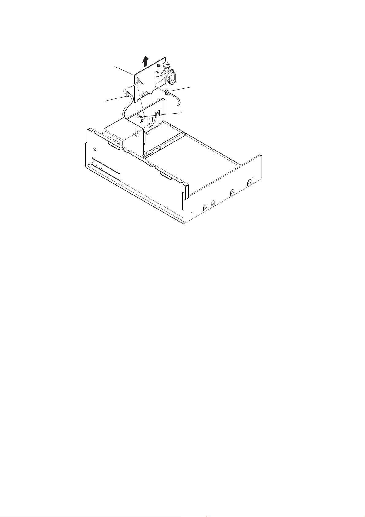
STR-DE898/DE998
2-6. STBY BOARD
4
2
STBY board
CNP815
3
1
CNP905
claw
12
Page 13
SECTION 3
96/24 Hz
RDS
-2 AAC OPT MONO
m
TEST MODE
STR-DE898/DE998
FACTORY PRESET MODE
* All preset contents are reset to the default setting.
* Procedure:
While depressing the [PRESET TUNING ---] and the [DISPLAY]
buttons simultaneously, press the ?/1 button to turn on the
main power.
The message “FACTORY PRESET” appears and the present contents are reset to the default values.
AM CHANNEL STEP 9 kHz/10 kHz SELECTION
MODE (US, CND, E2, AR model)
* Either the 9 kHz step or 10 kHz step can be selected for the AM
channel step.
* Procedure:
Turn the [INPUT SELECTOR] control to set AM and press the
?/1 button to turn off the main power.
While depressing the [PRESET TUNING +] button or the
[TUNING +] button, press the ?/1 button to turn on the main
power.
Either the message “9k STEP” or “10k STEP” appears for a
moment and select the desired step.
VACUUM FLUORESCENT DISPLAY TEST MODE
* All fluorescent segments are tested.
When this test is activated, all segments light on at the same
time, then each segment lights on one after another.
* Procedure:
While depressing the [TUNING ---] and the [SPEAKERS $OFF/A/
B/A+B%] buttons simultaneously, press the ?/1 button to turn on
the main power.
1. ALL segments light on.
SP. A SP. B
MULTI CH IN 12 EQ D.RANGE DIGITAL EX DTS-ES MPEG -2 AAC OPT COAX MONO
SLEEP A.DIRECT NIGHT MODE PROLOGIC IIx 96/24 NEO:6 kHz MHz D.ASSIGN STEREO
LFE
SW
CR
L
SL S SR
SBL SB SBR
D
D
D
D
[2CH], [A.F.D.], [MOVIE], [MUSIC], [MULTI CHANNEL DECODING], [VIDEO 1], [VIDEO 2], [VIDEO 3], [DVD], [TV/SAT], [MD/
TAPE], [SA-CD/CD], [TUNER FM/AM] and [PHONO] LED light
on.
MEMORY
RDS
dB
ft.
m
3. Press the [DIMMER] button, confirm display.
[2CH], [MOVIE], [VIDEO 1], [DVD], [MD/TAPE] and [TUNER FM/
AM] LED light on.
4. Press the [DIMMER] button, all segments and all LEDs light off.
5. Every Pressing the [DIMMER] button, turns on each segment
and LED one after another in the same order.
SOUND FIELD CLEAR MODE
* The preset sound field is cleared when this mode is activated.
Use this mode before returning the product to clients upon
completion of repair.
* Procedure:
While depressing the [2CH] button, press the ?/1 button to turn
on the main power.
The message “S.F. INITIALIZE” appears for a moment and initialization is performed.
SOFTWARE VERSION DISPLAY MODE
* The software version is displayed.
* Procedure:
While depressing the [TUNING ---] and the [DISPLAY] buttons
simultaneously, press the ?/1 button to turn on the main power.
The model name, destination and the software version are displayed.
COMMAND MODE SELECTION MODE
* The command mode (AV1 or AV2) of the remote commander
can be selected.
* Procedure:
While depressing the [ENTER] button, press the ?/1 button to
turn on the main power.
Either the message “C.MODE.AV1” or “C.MODE.AV2” appears
for a moment and select the desired mode.
2. Press the [DIMMER] button, confirm display.
A
SLEEP A.DIRECT NIGHT MODE PROLOGIC x
LFE
LSWR
S
SB
D
EQ DIGITAL
D
D
D
[A.F.D.], [MUSIC], [MULTI CHANNEL DECODING], [VIDEO 2],
[VIDEO 3], [TV/SAT], [SA-CD/CD] and [PHONO] LED light on.
13
Page 14
STR-DE898/DE998
d
4-1. CIRCUIT BOARDS LOCATION
SECTION 4
DIAGRAMS
POWER KEY board
HP board
V3 board (DE898)
FRONT AV board (DE998)
STBY board
OPT3 board
AC SEL board
(E2 model)
DISPLAY board
VOLUME board
SPEAKER board
VIDEO board
S-VIDEO board
VIDEO (AU) boar
DIGITAL board
AV SYNC JRC board
MAIN board
14
Page 15
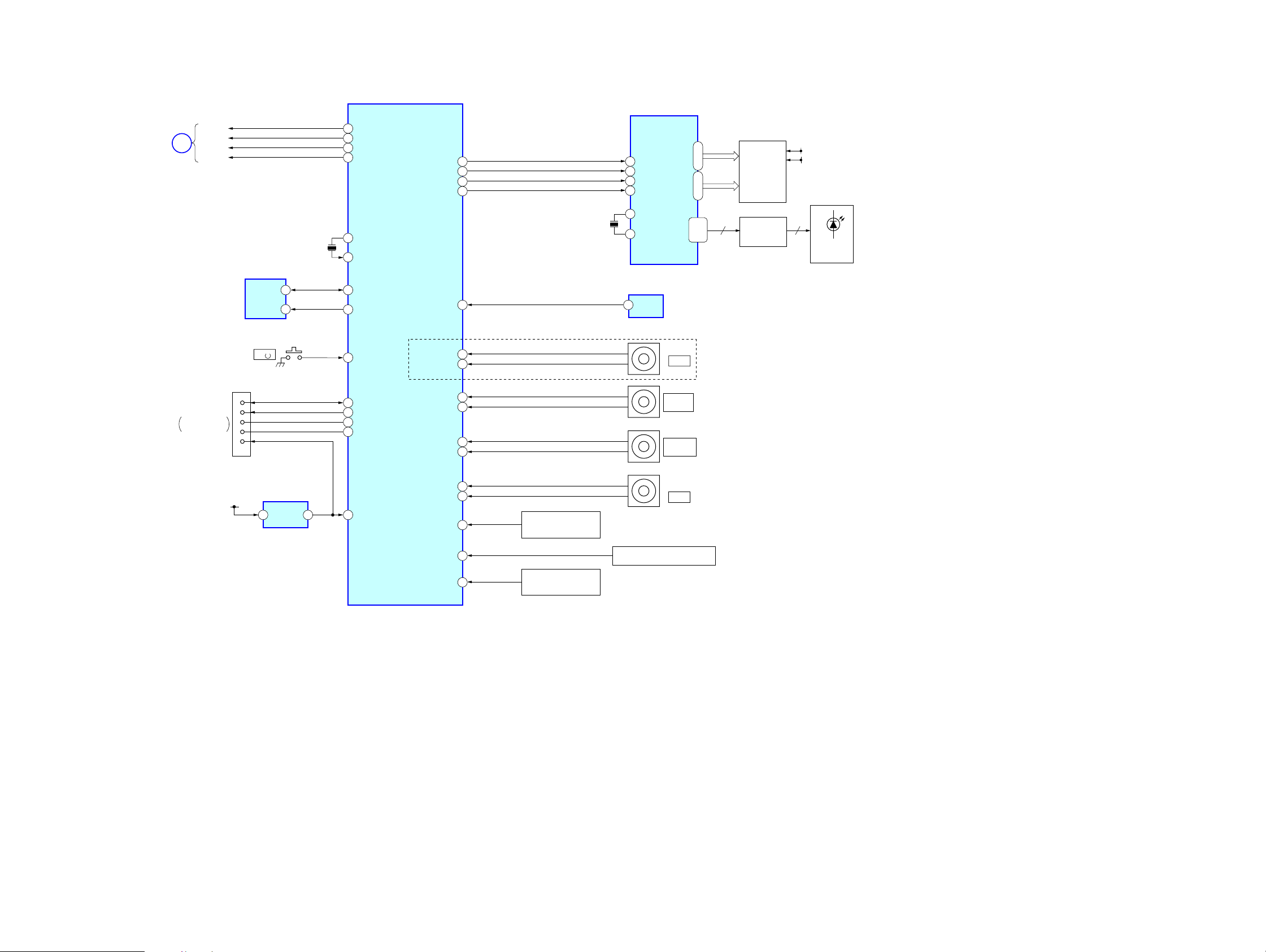
4-2. BLOCK DIAGRAM — TUNER/AUDIO SECTION —
STR-DE898/DE998
ANTENNA
FM 75Ω
COAXIAL
TU+10V
J2702 (2/3)
(DE998)
J2052 (2/2)
(DE898)
AM
VIDEO 3
INPUT
AUDIO
LR
R-CH
TN1
FM/AM TUNER UNIT
L-CH
R-CH
STEREO
TUNED
MUTING
CE
DO
DATA
CLOCK
R-CH
VIDEO 1
AUDIOINAUDIO
LR
LRLR
R-CH
28
TUNER_STEREO
29
TUNER_AUTO_STOP
30
TUNER_MUTE
T.LAT
34
31
TUNER_DO
T/LIP DAT
33
TUNER/LIP CLK
32
WOOFER_RY
22
-1-1-2-2-3 -4 -5 -6
LR LR LR
FRONT SURROUND
OUT
R-CH
AUDIO
R-CH
SYSTEM
CONTROL
IC1101 (1/5)
VIDEO 2
IN
J2553 J2552
R-CH
VOL_IC.DATA
R-CH
SURR BACK
MULTI CH IN
AUDIO
OUT
LR LRLR
-5 -6 -3 -4 -1 -2-5 -6 -3-3 -4 -1 -2-2
2ND RY
41
7.1_DAT
7.1_CLK
VOL_IC.CLK
116
117
R-CH
J304
1
2
DVD
AUDIOINAUDIO
R-CH
CENTER
R-CH
SUB
WOOFER
TV/SAT
IN
J305
(1/2)
R-CH
2ND
ZONE
8
6
17
4
15
2
12
RELAY
DRIVER
Q300
OUT
TV/SAT
DVD
VIDEO 2 OUT
VIDEO 2
VIDEO 1 OUT
VIDEO 1
VIDEO 3
DAT
22 23
J305 (2/2)
-3
L
-4
R
CLK
RY300
R-CH
AUDIO
AUDIO
SELECTOR
IC2560
AUDIO
OUT
2ND ZONE AMP
1 3
IN
10
13
1
4
6
8
3
DIGITAL
SECTION
(Page 16)
IC300
MD/TAPE
OUT IN
L
DIR
FUNCTION SELECT
19
46
38
SEL
SW
36
60
MCU
I/F
59
IC401
SEL
L
SEL
SL
+7V-7V
68 66
VCCVEE
R-CH
R-CH
R-CH
R-CH
R-CH
44
45
22
23
32
26
41
42
88
87
85
84
RL
-1 -2 -3 -4
R
J302
PHONO AMP
IC301
1 3
L-IN
R-IN
L-CH
R-CH
SL-CH
SR-CH
-1 -2 -3 -4
A
B
PHONO
L
DIGITAL
SECTION
(Page 16)
POWER
SECTION
SA-CD/CD
IN IN
RL
R-CH
R
J301
R-CH
(Page 20)
86
C
SW
SEL
SEL
R-CH
81
83
82
5 7
SUB WOOFER
SEL
SW
SBL
SEL
54 56 51 52 49
SBL OUT
SW OUT
C OUT
C
SL OUT
L OUT
AMP
IC604
C-CH
SBL-CH
SBR-CH
RELAY
DRIVER
Q351
RY351
J306
PRE
OUT
SUB
WOOFER
STR-DE898/DE998
• Signal path
: TUNER (FM/AM)
: VIDEO (AUDIO)
: CD (ANALOG)
• R-ch is omitted due to
same as L-ch.
15 15
Page 16
STR-DE898/DE998
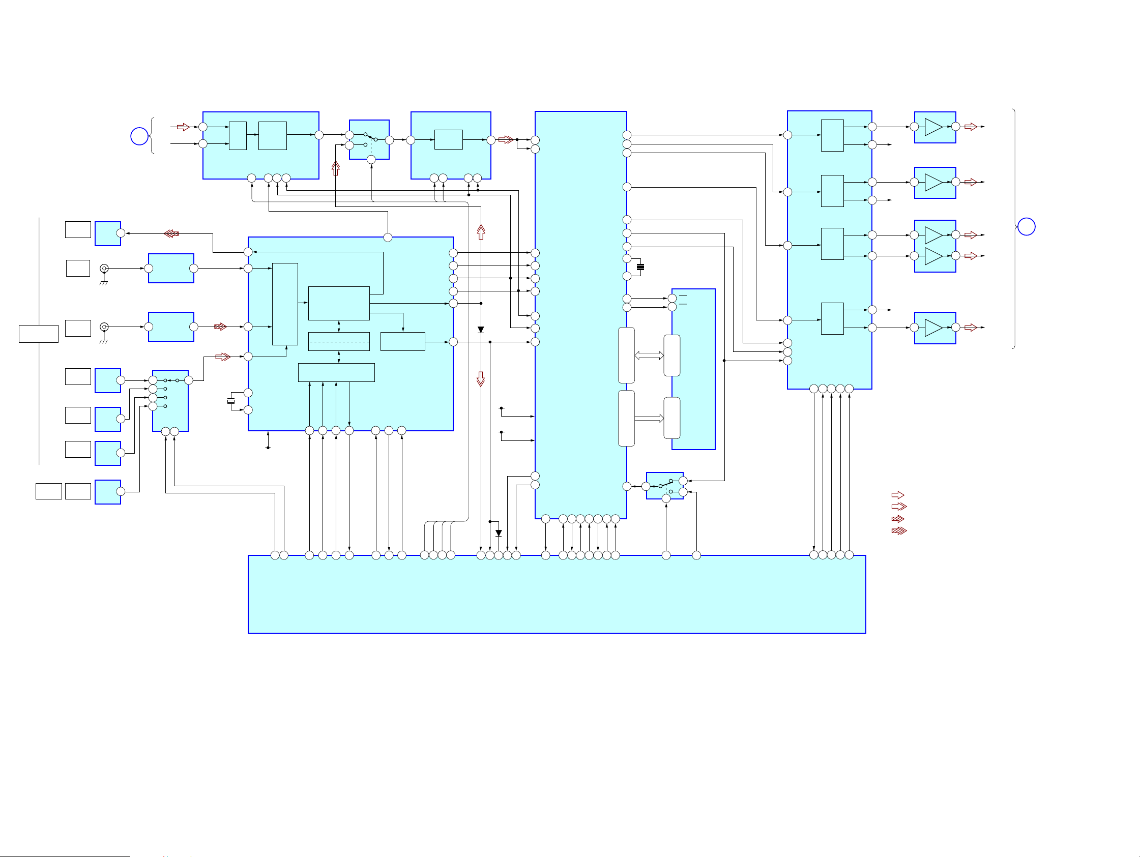
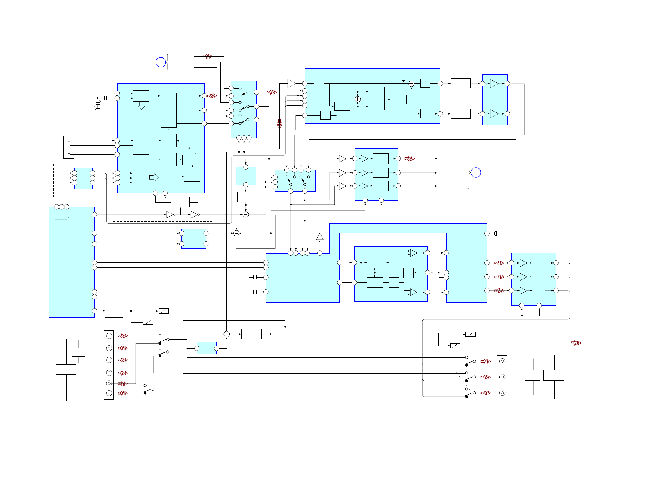
4-3. BLOCK DIAGRAM — DIGITAL SECTION —
DIGITAL
(ASSIGNABLE)
VIDEO 3
INPUT
MD/TAPE
OUT
(OPTICAL)
DVD
IN
(COAXIAL)
SA-CD/CD
IN
(COAXIAL)
SA-CD/CD
IN
(OPTICAL)
TV/SAT
IN
(OPTICAL)
MD/TAPE
IN
(OPTICAL)
DIGITAL
(OPT)
TUNER/
SECTION
(Page 15)
IC1353
J1301
-1
J1301
-2
IC1354
IC1351
IC1352
IC2010
AUDIO
DIN
OUT
OUT
OUT
OUT
DATA3
DATA1
DATA2
DATA4
SCKI
BCK
LRCK
8CH DAC
IC1452
MDO
MDI
34
DAC
DAC
DAC
DAC
35
MC
AMP
IC1403
VOUT5
10
VOUT6
9
14
13
20
16
ML
RST
3633
37
2
R-CH
5
R-CH
312
511
R-CH
5
AMP
IC1405
AMP
IC1404
AMP
IC1406
1
7
L OUT
SL OUT
TUNER/
C
1
7
7
C OUT
SW OUT
SBL OUT
AUDIO
SECTION
(Page 15)
• Signal path
: TUNER (FM/AM)
: VIDEO (AUDIO)
: CD (ANALOG)
ADC
IC1401
L IN
L-IN
A
R-IN
3
IC1303
WAVE
SHAPER
IC1373
WAVE
SHAPER
SELECTOR
IC1302
1
1
1
1
6 7
4
5
3
AB
14 2
1
5
23
23
X1301
12.288MHz
R IN
∆Σ
MOD.
DIGITAL
RST
6
DIGITAL AUDIO
I/F RECEIVER
DOUT
2
DIN2
5
DIN1
4
DIN0
3
21
XOUT
22
XIN
+3.3V
DECIM.
FILTER
SYSCLK
16
IC1301
VDD
DOUT
15
BCK14LRCK
13
INPUT
DEMODULATOR
Pa,Pb DETECTION LOCK
C bit DETECTION
MICROPROCESSOR
CLKCEDI
38 37 36 35 47 17
PCM RST
DATA
I/F
DO
2
1
SWITCH
IC7002
6
LAT
5
20
DETECTION
CKSEL1
2 18
XMCK
XMODE
XSTATE
48
SDI
AUDIO
CKOUT
LRCK
DATAO
ERROR
LIP SYNC
IC7001
DELAY
RST1BYP16BCKI
BCK
SDO
RAM
24
13 22
14 29
15 28
16
34 59
18
LRI
6
3
D1301
+2.6V
+3.3V
D1103
VDDI
VDDE
30
69
15
17
37
7
SDI1
SDI2
GP8
KFSI0
BCKI2
LRCKI2
LRCKI1
BCKI1
EXLOCK
GP12
PLOCK
68
GP9
HCS
DSP
IC1501
HACN
XRST
2 11336 35 33 3432
PM
SD01
SD02
SD03
SD04
SCKOUT
LRCKO
BCKO
MCLK1
MCLK2
CSO
WEO
HDIN
HDOUT
D0-15A0-15
BST
HCLK
23
24
25
26
14
19
20
9
X1502
13.9MHz
12
44
45
98,80 - 77,75 - 72
108,107,105 -102,99,
85-82,66 - 64
112,110,109,97 - 92,
SWITCH
IC1503
56
5
6
SDRAM
IC1502
CS
6
17
WE
D0-15A0-15
16-13,10 - 7
29 - 32,35 - 38,
1 - 5,18 - 21
24 - 27,42 - 44,
LRCKO
2
1
47
45
46
31
38
40
41
: CD (DIGITAL)
• R-ch is omitted due to
same as L-ch.
47
48
TC74HCT153_A
TC74HCT153_B
84 67 92 61
DIR CE
NO USE
DIR_CLK
NO USE
83
DIR CKSEL1
8281
DIR_XMODE
DIR_XSTATE
XRST
LAT
PCM RST
8785
LIP LATCH
PCM1800 RST
BYP
6
LIP RESET
LIP DATA IN
80
ERROR
DIR_DATAO
A_D
49
79
GP12
9718.PLLI
7471 119
9718.GP9
72 7376 104103 10278
XRST1
9718.HCS1
9718.HACN1
PM1
HDOUT
HDIN
9718.HCLK
BST SEL
SYSTEM
CONTROL
IC1101 (2/5)
75121
9718.BST1
8891
89
90
PCM1609 ML
PCM1609 MC
PCM1609 MDI
PCM1609 MDO
93
PCM1609 RST
STR-DE898/DE998
1616
Page 17
4-4. BLOCK DIAGRAM — VIDEO SECTION —
VIDEO
SELECTOR
IC3201
V1 IN
13
LD
5
TV
3
V2 IN
9
V3
7
V1.IN
13
LD
5
TV
3
V2 IN
9
V3
7
V1
13
LD
5
TV
3
V2 IN
9
V3
7
VIDEO 1
DVD
TV/SAT
DE998
VIDEO
INPUT
VIDEO 1
DVD
TV/SAT
VIDEO 2
VIDEO 3
INPUT
-2
S-VIDEO
IN
-2
S-VIDEO
IN
-1
S-VIDEO
IN
S-VIDEO
J3103 (1/2)
-2
VIDEO
IN
J3101
-2
VIDEO
IN
-1
VIDEO
IN
J3102 (1/2)
-2
VIDEO
IN
J2702 (1/3) (DE998)
J2052 (1/2) (DE898)
-1
VIDEO
J2106 (1/2)
Y
C
J2105 (1/2)
Y
C
J2105 (2/2)
Y
C
J2702 (3/3)
Y
C
G
G
G
G
G
G
SW2
SW3
SW4
SW4
S-VIDEO Y SWITCH
SW4
SW4
S-VIDEO C SWITCH
SW4
SW4
SW1
D3201,3202
SW1
IC2101
SW1
SW1
IC2102
SW1
SW1
OR
OR
D2102,2103
10 6 14 2
4
SW2
SW3
SW3
SW2
10 6 14 2
4
SW2
SW3
SW3
SW2
10 6 14 2
4
SW3
SW2
SW5
SW5
SW5
6dB AMP
6dB AMP
6dB AMP
6dB AMP
6dB AMP
6dB AMP
6dB AMP
75Ω
DRIVER
75Ω
DRIVER
75Ω
DRIVER
75Ω
DRIVER
75Ω
DRIVER
75Ω
DRIVER
75Ω
DRIVER
V1.OUT
M.OUT
V2.OUT
V1.OUT
M.OUT
V1.OUT
M.OUT
STR-DE898/DE998
VCC
+5V-3
15
1
11
VEE
-5V-3
VCC
+5V-3
15
1
VEE
-5V-3
VCC
+5V-3
15
1
VEE
-5V-3
+5V-3
IC3103
3 1
+5V
REG
+9V
J3103 (2/2)
J3102 (2/2)
J2106 (2/2)
Y
C
J2104
Y
C
IC3102
+9V
3 1
REG
VIDEO
OUT
VIDEO
OUT
VIDEO
OUT
SW1
SW2
SW3
SW4
G
S-VIDEO
G
MONITOR-V/IN
MONITOR-Y/IN
MONITOR-C/IN
MONITOR-V/OUT
MONITOR-Y/OUT
MONITOR-C/OUT
G
S-VIDEO
G
-5V-3
-1
-3
-1
-1
OUT
OUT
VIDEO 1
MONITOR
VIDEO 2
V SW1
V SW2
V SW3
V SW4
VIDEO 1
MONITOR
IC3101
+12V
3 1
REG
IC3104
-5V
3 2
REG
KEY/DISPLAY
E
SECTION
(Page 18)
OSD
F
SECTION
(Page 19)
OSD
D
SECTION
(Page 19)
+15V
-15V
• Signal path
: VIDEO
STR-DE898/DE998
17 17
Page 18
STR-DE898/DE998
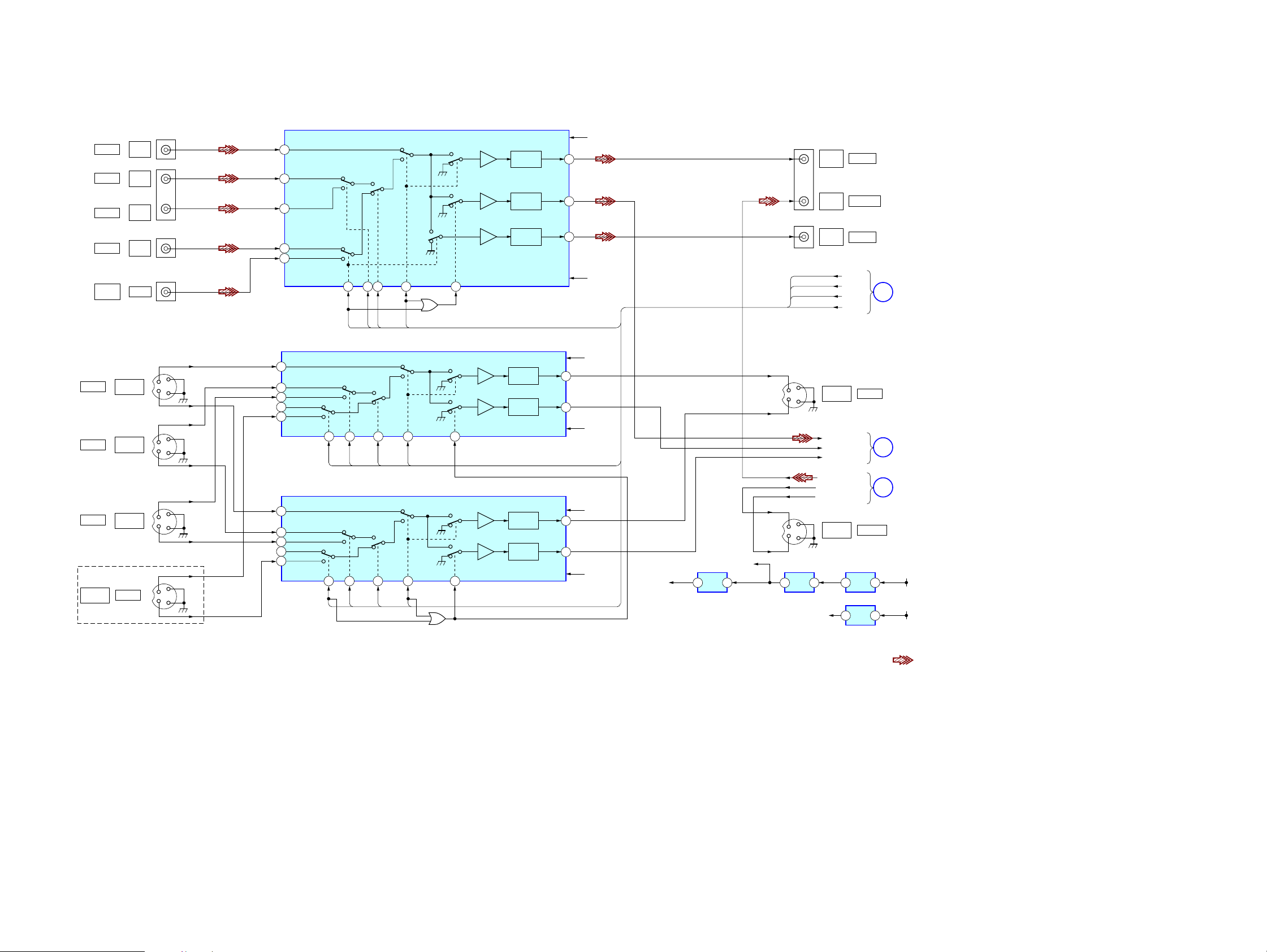
4-5. BLOCK DIAGRAM — KEY/DISPLAY SECTION —
VIDEO
SECTION
(Page 17)
SYSTEM
V.SW1
V SW1
V SW2
E
V SW3
V SW4
X1101
16.5MHz
EEPROM
IC1131
5
SDA
SCL
6
S141
I
/
I
36
V.SW2
37
V.SW3
38
V.SW4
39
57
X1
X0
58
EEPROM.SDA
99
EEPROM.SCL
100
62
PW_ON/OFF
CONTROL
IC1101 (3/5)
FL LAT/F2
FL DIN/F1
FL CLK
FL DRV.CLR
MENU _JOG_3A
MENU_JOG_3B
SIRCS
113
112
114
115
X101
8MHz
63
DE998
13
12
SIRCS
FL DISPLAY DRIVER
IC100
P51
19
P15
15
P17
17
RESET
8
XIN
2
XOUT
3
OUT
1
1
3
P1
I
P21
G1
I
G16
P00,01
P03-07
P40,41
P43-47
REMOTE
CONTROL
RECEIVER
IC103
RV101
MENU
61
I
41
77
I
62
22,23
25-31
33-37
14
FL101
VACUUM
FLUORESCENT
DISPLAY
LED DRIVE
Q101,103-106,
108-116
F1
F2
14
D101,103-106,
108-116
FLASH
PROGRAMMING
CNS503
+3.3V
(STBY)
1
3
1
3
1
3
AD0
AD1
AD2
132
133
134
17
16
11
10
15
14
SW NETWORK
S100,102-107
S101 (DE998)
SW NETWORK
S122-125
S126,127 (DE898)
FLASH1
1
FLASH2
2
MD2
7
MD0
6
RESET
5
IC1111
12
RESET
109
110
SOT1
SIN1
MD2
52
MD0
54
55
RSTX
VOL_JOG_2A
VOL_JOG_2B
FUNCTION_JOG_1A
FUNCTION_JOG_1B
CURSOL_JOG_4A
CURSOL_JOG_4B
RV103
MASTER
VOLUME
RV104
INPUT
SELECTOR
RV102 (DE898)
RV105 (DE998)
-/+
SW NETWORK
S110-116
STR-DE898/DE998
1818
Page 19
4-6. BLOCK DIAGRAM — OSD SECTION —
STR-DE898/DE998
(DE998)
EXCEPT
DE898:
US,CND
MODEL
(TEST)
106105 107
DATA
OSD
SYSTEM
CONTROL
IC1101 (4/5)
CNP3501
1
2
4
LAT
CLK
X3501
14.31MHz
CT3502
V SYNC
H SYNC
TEST
IC1141
9
12
BUFFER
2
OSD
ON/OFF
UP MUTE
M MUTE
UPCON DATA
UPCON CLK
V MUTE
COMP SEL2
COMP SEL1
IC3501
4
RY3303
F
ANALOG
VIDEO
SIGNAL
DISPLAY
MEMORY
CONTROL
DATA
7
Q3502
MONITOR-V/IN
MONITOR-Y/IN
MONITOR-C/IN
SW
GEN
POWER SW
Q3501
V OUT
Y OUT
C OUT
OUTPUT
CONTROL
CG ROM
CHARACTER
VRAM
IC2102
3
SHIFT
1
Q3503
UP
5V-3
Y/C SEPARATION
IC3601
MONITOR SELECTOR
IC3651
12
25
27
26
4
2
13
2
1
5
3
SEPARATION
X3701
3.5795MHz
(US,CND MODEL)
(EXCEPT US,CND MODEL)
CBA
9 10 11
IC3731
1
SYNC
2
SYNC DET
Q3731
MUTE CONTROL
Q3677,3678
X302
4.43MHz
14
15
4
37
36
26
28
A
11
B
10
C
9
UP CONVERT
SELECTOR
IC3751
SDA
SCL
XNTSC
X443/358
Q3601,3604
2
17
DATA
19
CLK
23
LAT
26
37
3
5 13
4
14
H/V
SEPA
Q3701
32 34 39 38 30
C
CVBS/Y
H SYNC
AD
IN
MOD2
MOD1
PNR
NTPL2
12
V SYNC
ADC
PLL
Q3651-3653
–(R,Y)
SECAM
–(B,Y)
I LINE
MEMORY
SYSTEM
CLOCK
Q3671,3672
Q3673,3674
Q3675,3676
24
23
VIDEO AMP
7
4
1
MUTE2 MUTE1
16
14
DYNAMIC
COMB
FILTER
IC3671
DRIVER
DRIVER
DRIVER
LINE
MEMORY
LINE
MEMORY
EXCEPT US,CND MODEL
75Ω
75Ω
75Ω
310
DELAY LINE
IC3721
S/H
S/H
COLOR
KILLER
AYO
DAC
9
ACO
DAC
7
11
13
15
PLL
MONITOR-V/OUT
MONITOR-C/OUT
MONITOR-Y/OUT
UP CONVERTER
IC3701
11
5
12
21
16
10
22
LPF
Q3621,3622
LPF
Q3631,3632
–(R,Y)
SCPN
CPIN
–(B,Y)
D
CERA
VIDEO AMP
IC3741
1
8
VIDEO
SECTION
(Page 17)
1
Y
U2
V2
4
5
X3703
500KHz
1 1118
4 137
7
MUTE1 MUTE2
VIDEO AMP
IC3321
DRIVER
DRIVER
DRIVER
10 3
75Ω
75Ω
75Ω
Y
U2
V2
156
(Page 17)
EXS
8
XS
9
11
10
TEST
21
DATA
8
CLK
11
LAT
3
108
86
87
43
111
64
40
66
23
22
24
RELAY
CONTROL
Q3302
SIN
SCLK
CS
VIDEO
SECTION
ON SCREEN DISPLAY CONTROL
4FSC
OSC
COLOR
BURST
NTSC/
PAL
SIGNAL
GEN
SERIAL
INPUT
CONTROL
AVCC VCC
RY3304
COMPONENT
VIDEO
STR-DE898/DE998
TV/SAT
IN
DVD
IN
P
B/CB
/B-Y
PR/CR/R-Y
PB/CB/B-Y
P
R/CR
/R-Y
J3104 (1/2)
-1
Y
-2
-3
-4
Y
-5
-6
IC3253
SYNC
1 2
SEP
SYNC DET
Q3252
RELAY CONTROL
Q3301,3304
19 19
RY3301
RY3302
J3104 (2/2)
-7
Y
U2
V2
Y
-8
-9
MONITOR
B/CB
/B-Y
P
R/CR
/R-Y
P
OUT
COMPONENT
VIDEO
• Signal path
: VIDEO
• Abbreviation
CND:Canadian model
Page 20
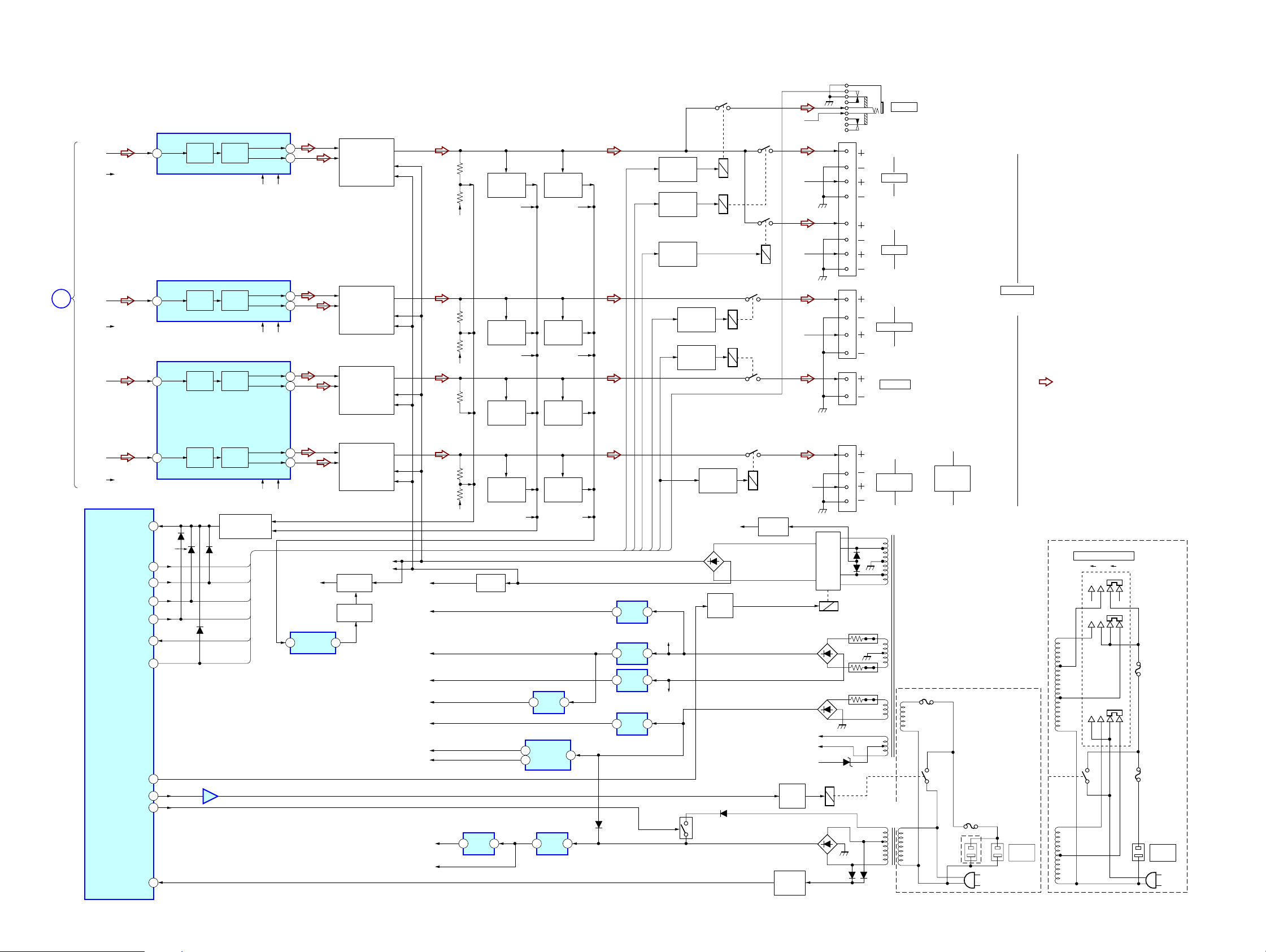
STR-DE898/DE998
4-7. BLOCK DIAGRAM — POWER SECTION —
PRE DRIVER
IC500
IN 2
PRE
PRE DRIVER
IC600
PRE
PRE DRIVER
IC400
PRE
PRE
Q200-202,255,256
D1110
FRONT A RY
REAR-RY
CENTER RY
FRONT B RY
IC2102
56
DRIVE
DRIVE
DRIVE
DRIVE
PROTECTOR
D201-203
HP-RY
HP CTRL
-48V +48V
-48V +48V
-48V +48V
TUNER/
AUDIO
SECTION
(Page 15)
B
L-CH
R-CH
SL-CH
SR-CH R-CH
C-CH
SBL-CH
SBR-CH
SYSTEM
CONTROL
IC1101 (5/5)
BRIDGEABLE RY
VOLT_DETECT_STOP
R-CH
R-CH
(IC700)
PROTECTOR
HP_RY
SP_A_RY
REAR_RY
CENTER_RY
HP_CTRL
SP_B_RY
PW-RY
SUB-T
23
42
18
21
20
24
19
45
25
5
60
8
8
6
8
D1107
D1108
IN 2
IN1
IN2
DRIVE
DRIVE
DRIVE
DRIVE
D1111
+VOUT2
-VOUT2
+VOUT2
-VOUT2
+VOUT1
-VOUT1
+VOUT2
-VOUT2
12
11
12
11
2
3
12
11
IC210
OVERLOAD
DETECT AMP
+48V
POWER AMP
Q571-574
POWER AMP
Q671-674
POWER AMP
Q421-424
POWER AMP
Q471-474
+48V REG
Q220,225
PROTECTOR
Q210
72
J2501
PHONES
R-CH
TM2880
TM601
L
FRONT B
R
L
FRONT A
R
L
SURROUND
R
CENTER
SPEAKERS
IMPEDANCE
USE 8-16Ω
• Signal path
: TUNER (FM/AM)
R-CH
R-CH
CURRENT
DETECT
Q575,576
R-CH
CURRENT
DETECT
Q675,676
R-CH R-CH
OVERLOAD
DETECT
D575,Q577
R-CH
OVERLOAD
DETECT
D675,Q677
RELAY
DRIVER
Q240
RELAY
DRIVER
Q2880
RELAY
DRIVER
Q2881
RELAY
DRIVER
Q600
RELAY
DRIVER
Q400
RY240
RY2881
RY600
RY400
R-CH
R-CH
RY2880
TM602(1/2)
R-CH
• R-ch is omitted due to
CURRENT
DETECT
Q425,426
CURRENT
DETECT
Q475,476
R-CH
+B
-B
-48V
TU+10V
+7V
-7V
+5V-2
+5V-1
+2.6V
+3.3V
+3.3V
(STBY)
+5V
(STBY)
IC1021
+3.3V
REG
R-CH R-CH
-48V REG
Q235
13
5
+2.6V/+3.3V
2
OVERLOAD
D425,Q427
OVERLOAD
D475,Q477
IC1001
+5V
REG
IC1901
REG
IC1011
+5V
REG
DETECT
DETECT
13
TM602(2/2)
D925
D251
D290
D291
R861
R862
R851
L
SURROUND
BACK
R
(DE898) (DE998)
T901
POWER
TRANSFORMER
(EXCEPT E2 MODEL)
T902
POWER
TRANSFORMER
D926
F901
SURROUND
BACK
(2ND ZONE)
US,
CND
MODEL
F902
AC IN
~
-30V
RY700
-30V REG
Q250
D851-854
RELAY
DRIVER
Q911
D921-924
VOLTAGE
DETECT
Q921
R-CH
RECT
D865
RECT
RECT
RY802,803
F1
F2
-30V
RELAY
SWITCH
RY911
RELAY
DRIVER
Q700
HP-RY
FRONT B RY
FRONT A RY
REAR-RY
CENTER RY
HP CTRL
RECT
D801,802
IC1902
+10V
13
REG
IC260
REG
REG
IC265
IC1031
REG
4
D1001
13
+7V
-7V
+5V
+15V
13
23
-15V
13
RELAY
DRIVER
Q809
D927
+B SWITCH
Q912,913
same as L-ch.
• Abbreviation
CND: Canadian model
E2 : AC 120V area in E model
( E2 MODEL)
VOLTAGE SELECTOR
240V 220V 120V
-2
-3
240V
220V
120V
-1
0V
J911
AC
OUTLET
S901
F904
F902
J911
AC
OUTLET
AC IN
~
STR-DE898/DE998
2020
Page 21
STR-DE898/DE998
THIS NOTE IS COMMON FOR PRINTED WIRING
BOARDS AND SCHEMATIC DIAGRAMS.
(In addition to this, the necessary note is
printed in each block.)
for schematic diagram:
• All capacitors are in µF unless otherwise noted. (p: pF)
50 WV or less are not indicated except for electrolytics
and tantalums.
• All resistors are in Ω and 1/
specified.
f
•
• 2 : nonflammable resistor.
• 5 : fusible resistor.
• C : panel designation.
• A : B+ Line.
• B : B– Line.
•Voltage and waveforms are dc with respect to ground
•Voltages are taken with a VOM (Input impedance 10 MΩ).
•Waveforms are taken with a oscilloscope.
• Circled numbers refer to waveforms.
• Signal path.
•Abbreviation
: internal component.
Note:
The components identified by mark 0 or dotted
line with mark 0 are critical for safety.
Replace only with part
number specified.
under no-signal (detuned) conditions.
no mark : FM
Voltage variations may be noted due to normal production tolerances.
Voltage variations may be noted due to normal production tolerances.
F : TUNER (FM/AM)
L : VIDEO (AUDIO)
I : VIDEO
J : CD (ANALOG)
c : CD (DIGITAL)
CND : Canadian model.
E2 : AC 120V area in E model.
AR : Australian model.
AUS: Australian model.
SP : Singapore model.
MY : Malaysia model.
4
W or less unless otherwise
Note:
Les composants identifiés par
une marque 0 sont critiques
pour la sécurité.
Ne les remplacer que par une
piéce portant le numéro
spécifié.
for printed wiring boards:
• X : parts extracted from the component side.
f
•
• : Pattern from the side which enables seeing.
Caution:
Pattern face side: Parts on the pattern face side seen from the
(Side B) pattern face are indicated.
Par ts face side: Parts on the parts face side seen from the
(Side A) parts face are indicated.
•Abbreviation
: internal component.
CND : Canadian model.
E2 : AC 120V area in E model.
AR : Australian model.
AUS: Australian model.
SP : Singapore model.
MY : Malaysia model.
C
Q
B
E
Q
BCE
Q
B
C
These are omitted.
These are omitted.
E
• Waveforms
— DIGITAL Board — — VIDEO Board —
1
1
IC1301 qd (CKOUT)
12.288MHz
1V/DIV, 50nsec/DIV
2
IC1301 qf (BCK)
3.07MHz
1V/DIV, 0.2µs/DIV
3
IC1301 wa (XOUT)
12.288MHz
1V/DIV, 50nsec/DIV
4
IC1501 9 (MCLK1)
13.9MHz
2.1Vp-p
3.2Vp-p
2Vp-p
2.2Vp-p
5
IC1501 qs (MCLK2)
13.9MHz
1V/DIV, 50nsec/DIV
6
IC1501 qf (SCKOUT)
12.288MHz
1V/DIV, 50nsec/DIV
7
IC1101 tj (X1)
16.5MHz
1V/DIV, 50nsec/DIV
3.5Vp-p
2.3Vp-p
1.8Vp-p
IC3501 8 (EXS)
14.31MHz
1V/DIV, 20nsec/DIV (ON SCREEN: ON)
2
IC3701 1 (CERA)
500kHz
1V/DIV, 2µsec/DIV
3
IC3701 wh (XNTSC)
3.5795MHz
1V/DIV, 0.2µsec/DIV
4
IC3701 wk (X443/358)
4.43MHz
1.5Vp-p
1.2Vp-p
1.6Vp-p
1.6Vp-p
STR-DE898/DE998
1V/DIV, 50nsec/DIV
— DISPLAY Board —
1
1V/DIV, 20nsec/DIV
21 21
IC100 3 (XOUT)
8MHz
1V/DIV, 0.2µsec/DIV
0.5Vp-p
Page 22
STR-DE898/DE998
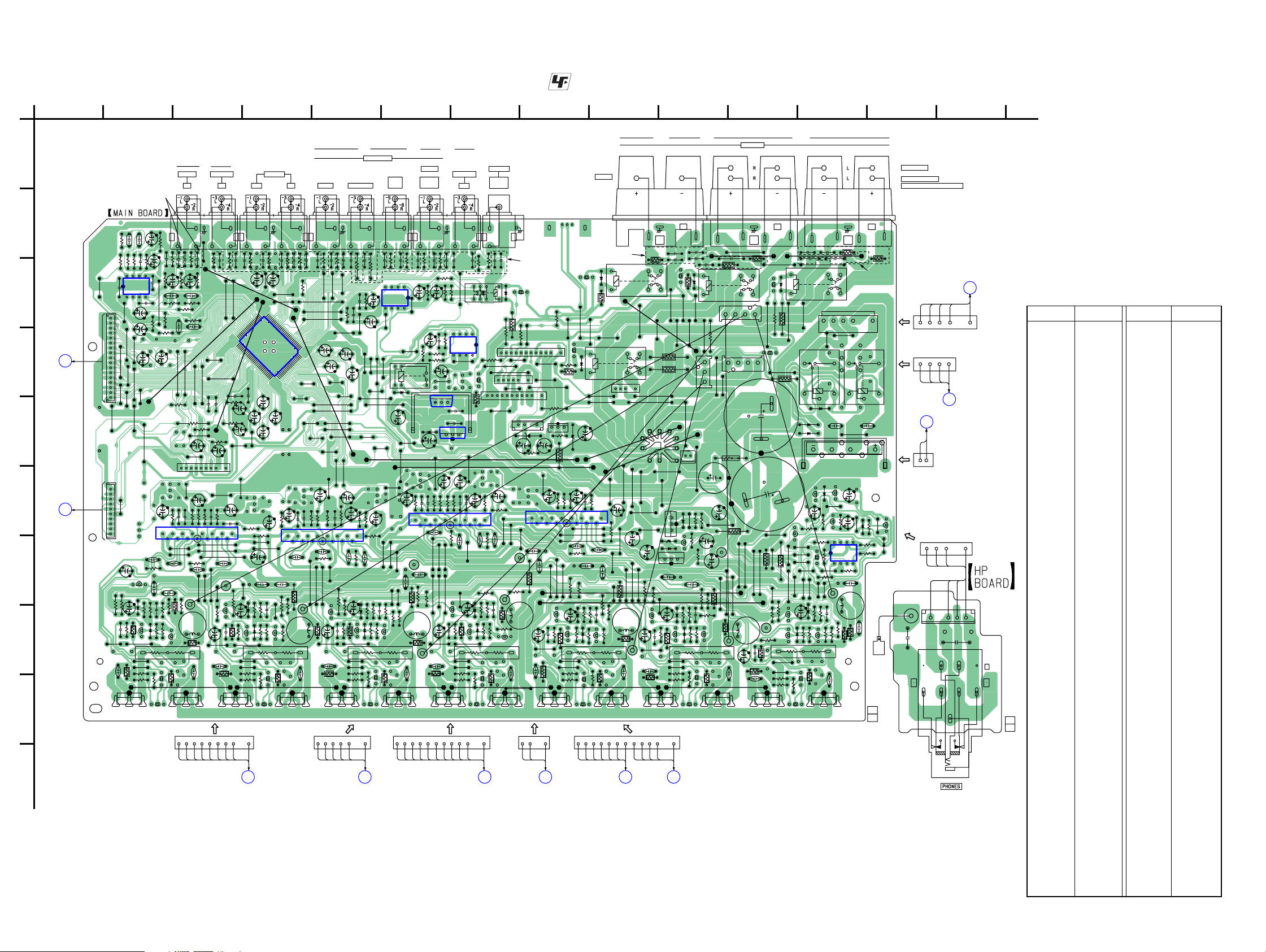
4-8. PRINTED WIRING BOARDS — MAIN SECTION —
1
234567891011121314
A
B
C
D
E
F
G
H
J
J301
SA-CD/CD
PHONO 2ND ZONE
AUS,AR,SP,MY
MODEL
C304
306
C306
C307
R
C303
307
304
303
305
R
R
R
R
C305
14
IC301
401
C309
85
JW
DIGITAL
A
BOARD
CNS501
(Page 27)
DIGITAL
B
BOARD
CNS502
(Page 27)
I
C355
C358
400
JW
C308
308
R
P811
CN
405
JW
406
JW
404
JW
C486
456
JW
402
JW
411
309
410
JW
JW
JW
413
312
JW
JW
418
JW
10
422
JW
P814
CN
C465
C471
R465
Q477
C482
475
D
C477
485
486
R
496
484
R
R
R
476
R
477
475
C475
R
C473
473
R
Q473
JW329
JW607
JW608
R472
R471
Q
474
R
JW331
BECBECBECBECBECBECBECBE
IN IN IN
302
Q472
C476
476
D
C359
403
JW
C485
C466
R
351
R
C352
C353
352
R
C356
R355
358
R
R309
15
14
JW610
C464
C481
482
R
480
R
483
479
R
R
R478
471
Q
308
JW
301
C351
R
C302
C354
C357
354
R
R356
R357
R359
C310
C360
415
414
JW
JW
R409
R408
JW409
C479
JW420
495
R
466
C463
C462
R
IC400
JW611
R415
C415
487
R
CN450
481
R
L451
476
Q
475
R
Q474
91
Y
R
BLU
G
416
JW
R441
CNP812
C461
461
R
606
JW
ORG
R489
JWH420
Y
R
G
311
C301
R
R361
CC02
JWH404
353
R
408
JW
H403
JW
50
51
JW304
JW311
417
JW
C428
R658
C408
C409
R656
R440
C429
JW430
C478
19
JW455
C411
462
411
412
C412
C413
R
R
R
1
2
JW614
JW613
JW612
C414
CP805
604
605
JW
603
JW
JW
436
R
427
435
Q
R
427
C421
R
C425
JW601
C423
C474
R423
Q423 Q424 Q573
Y
Y
Y
Y
R
R
R
R
BLU
G
G
G
G
J302
MD/TAPE
313
363
31
C840
C490
JW615
446
R
433
R
Q422
426
JW
C416
434
R
429
R
424
R
30
80
CC363
C426
R428
C690
426
Q
R
IC401
81
421
Q
JW421
JW425
566
R
C431
598
JW
432
R
C363
C566
425
R
CC314
15
R430
14
C564
314
R
CC01
R
CC313
C313
407
JW
JWH402
C418
C390
C417
450
JW
445
R
R416
R400
JW616
C403
602
C432
JW
C427
425
D
426
425
R
Q
426
D
JW330
JW599
JW600
R422
R421
CNP812
Y
R
G
VIDEO (AU)
BOARD
CNP208
(Page 35) (Page 38) (Page 44) (Page 44) (Page 27) (Page 27)
• See page 14 for Circuit Boards Location. : Uses unleaded solder.
SURROUND
FRONT
551
451
401
R
C343
R
CC401
JW437
JW438
R512
C571
C573
R573
Y
R
G
C594
JW424
595
JW
577
Q
470
JW
Y
R
G
467
JW
C512
JW310
C544
511
R
R586
C578
Y
R
G
CC
620
JW
330
R
C331
C440
C540
545
595
R
R
C511
C516
1
2
C515
C577
585
R
576
R
577
R
JW587
JW588
JW589
R572
R571
Y
R
G
CC451
CC364
320
JW
R752
JW423
JW305
C640
C590
JW439
JW440
C494
JW432
C561
562
561
C562
R
R
IC500
C565
R565
333
597
596
JW
JW
JW
BLU
439
R
JW332
61
RY
G
1
C844
437
R
CN400
364
C341
R
JWH400
100
C444
C563
431
R
JW443
JW428
L401
C424
J304
MULTI CH IN
551
R
1
380
38
R
C
472
JW
445
JW
JW442
C694
C513
515
R
575
Q
ED
R
VIDEO
BOARD
CNP207
SURR
BACK
651
C651
R
C
CC501
CC601
R501
C380
58
IC300
41
7
45
JW
C330
JW479
RY351
444
446
JW
JW
D351
JW441
C261
JW447
C644
JWH405
449
JW
JW453
C666
593
594
JW
JW
CP804
592
JW
C581
591
590
581
R
JW
JW
580
587
C576
R584
R
R
582
R
579
576
R
583
Q
R
R589
R578
74
575
571
R
Q
R5
Q574
11 1
RY
RY
G
G
D575
Q572
R500
576
D
427
JW
C394
516
R
C503
C514
596
R
CN803
J305
OUTOUT
C677
JW573
J306
PRE OUT
SUB
WOOFER
AUS,AR,SP,MY
388
345
C
389
R
C333
CC374
R
RY300
503
JW
Q351
11
398
R
695
R
C613
C612
C616
1
2
665
C615
C
582
JW
R680
675
696
D
R
676
R
675
676
Q
D
R678
674
R
Q672
ED
RY
R
G
MODEL
Q300
300
D
342
R
341
R
605
R
JW468
CN507
R397
JW489
JW484
JW493
6
JW491
CN803
CNP804
JW539
CNP802
C252
R252
616
C603
R
R600
572
571
JW
570
JW
JW
C614
CP801
R687
CN650
GRY
676
C
R689
L651
R682
R679
Q676
C674
R675
JWH417
JW344
CBECBECBECBECBECBEC
Q674
31 12 65 1
L
YE
683
R
671
Q
615
R
684
R
CNP804
112
JW492
JW487
1
JW387
1
R825
Q250
E C B
13
D251
R251
C251
795
711
R
R
C711
IC700
15
14
C681
C682
575
564
574
681
JW
R
JW
JW
527
Q
C525
C521
527
R
526
JW350
R
JW578
523
C523
R
Q523 Q524
CNP802 CN507
RG
BRN
O
405
R
R245
R246
R250
JWH406
712
R
C715
C527
JW577
R522
R521
CENTER
AUS,AR,SP,MY
MODEL
Q400
400
D
406
R
436
497
JW
621
JW
JW498
JW
40
RY240
Q2
D240
4
JW617
JW325
C250
C532
525
D
3
53
R
JW567
35
5
R
546
R
6
52
D
Y
R
G
713
C
R528
21
Q5
JWH407
336
JW
6
71
R
1
C703
2
700
R
C714
566
JW
531
C
1
53
R
555
JW
530
6
537
R
R
534
C52
R
32
529
526
R
Q
R5
525
524
R
R
Y
Y
Y
R
R
R
G
G
GRYG
D250
12
C716
C7
JW568
JW569
R715
536
R
525
Q
Q522
Y
R
G
-1
CENTER
-2
SUB
WOOFER
751
601
701
C701
R
R
CC751
C382
471
JW
15
14
C582
L551
CN550
C575
JWH418JWH419
Y
RY
R
G
G
66
6
R
C664
D265
C266
686
R
C395
C663
Y
R
G
396
R
WHT
381
R
C332
C662
85
6
R
R673
C
R392
R391
IC260
645
R
C671
JW334
C673
R
R382
392
C
C391
R395
123
C661
1
662
66
R
R
IC600
335
584
JW
JW
586
576
JW
JW
Q673
Y
ED
R
R
G
C344
C383
331
332
R
R
390
R
58
IC604
41
JW458
C260
C265
IC265
123
C611
612
611
R
R
R665
583
JW
585
JW
81
5
JW
677
Q
C675
677
R
JW579
JW580
R672
R671
Y
RY
R
G
G
KJHG
STBY
BOARD
CNP813
T901
POWER
TRANSFORMER
DIGITAL
BOARD
CNP510
TM601
C600
C750
CN806
L501
R539
RY400
JW
94
4
JW
5
56
JW
C231
554
JW
CN500
JWH416
ED
R
RR81
JWH410
307
JW
5
51
JW
1
JW507
JW499
GP1
8
0
4
H
231
533
JW
JW
JW535
JW536
D221
C221
63
5
562
JW
6
JW
63
R
59
5
JW
627
Q
C621
625
RED
C
JW340
C623
24
C5
R623
Q623
Y
Y
Y
RY
R
R
R
G
G
G
G
R240
B
JW530
5
C632
63
R
C627
27
6
R
CC81
315
JW
R280
U
L
528
JW
235
Q
D220
Q220
E C B
JWH413
JW557
JW558
R622
R621
C300
CC21
600
0
D
60
Q
6
60
R
9
35
314
JW
JW
523
508
500
JW
JW
JW
T
H
W
RED
366
JW
12
CNP805
365
JW
5
B
236
35
23
2
R
JW
D
C
C233
E
5
36
2
22
R
Q
R222
C631
630
R
626
5
C
R632
634
646
62
R
R
D
625
26
Q
633
629
R
R
D6
626
R
R628
1
62
624
Q
R
Q622
ED
R
DC
DIGITAL
BOARD
CNP507
JWH412
824
R
1
3
C290
33
R2
C220
637
R
626
Q
ORG
301
N
C
C230
JW561
CN600
625
R
Q624
511
JW
CP803
351
JW
SPEAKERS
IMPEDANCE USE 8-16Ω
JW516
CC71
RR21
RY600
CN300
N
BR
CN851
512
JW
R290
R234
233
JW
549
548
JW
JW
JWH414
1
63
R
N
R
B
639
R
L601
C721
624
C
JWH415
RR71
2
23
JW
R723
C723
TM602
SURROUND
SURROUND BACK (DE898)
SURROUND BACK (2ND ZONE) (DE998)
C700
C400
JW316
00
00
7
7
Q
D
14
317
JW
705
R
V
IO
706
R
Q809
41
JW521
C804
C803
JW352
220
R
235
JW
545
556
JW
JW
30
6
JW
736
735
R
R
CP802
R727
725
C
726
R
JW550
JW551
R722
R721
Q723
JW513
RY700
09
322
5
JW
JW
RY803
R830
D818
D290
D291
C255
R204
255
Q
R210
JW255
21
JW540
R2
10
642
JW541
Q2
JW
JW210
3
43
54
46
6
5
547
JW
JW
W
JW
J
27
725
7
D
Q
C727
3
25
29
726
7
73
7
D
Q
R
R
R728
725
721
R
Q
24
R7
Q722
RR11
CC11
CC61
51
JW851
852
JW
C802
~~
D801
01
256
D2
Q
JW640
02
05
2
203
Q
R
R2
14
IC210
11
2
85
R
D210
R215
2
4
VIO
54
54
JW
JW
CN700
726
746
734
C
R
R
6
732
737
72
R
R
Q
724
C
Q724
1-865-743-
01
Q2
0
73
R
JWH411
CN908
C200
C201
R212
C732
39
7
R
L701
AUS,AR,SP,MY
MODEL
JW800
31
7
R
02
R2
R213
C731
C800
R214
RR61
RY802
01
202
2
D
R
(CHASSIS)
11
(11)
5
0
52
20
Q
JW
3
20
D
BLK
(Page 44)
T901
POWER
TRANSFORMER
I
G
R
LK
O
B
5
1
ED
LK
B
R
DIGITAL
BOARD
E
CNP506
U
BLU
BL
CNP805
2
1
41
Y
RY
GR
G
D
RE
TP700
502
2
C
YEL
LK
B
CNP701
ED
R
F
Y
GR
Y
GR
J2501
LU
B
CN851
4
SPEAKER
BOARD
CNP851
(Page 34)
(Page 27)
Y
GR
C2502
D
RE
1
ED
R
Y
R
G
41
CN806
CN908
1-865-751-
• Semiconductor Location
Ref. No. Location
D201 F-12
D202 F-12
D203 G-13
D220 G-10
D221 G-10
D235 F-10
D240 D-8
D250 E-8
D251 E-8
D265 E-6
D290 E-12
D291 E-12
D300 C-7
D351 D-6
D400 C-9
D425 H-4
D426 H-4
D475 G-2
D476 H-2
D525 H-8
D526 H-8
D575 H-5
D576 H-5
D600 C-10
D625 H-10
D626 H-10
D675 H-7
D676 H-7
D700 C-11
D725 H-12
D726 H-12
D801 E-12
D818 E-12
IC210 G-12
IC260 E-6
IC265 E-7
IC300 C-6
IC301 C-2
11
IC400 F-3
(11)
IC401 D-4
IC500 F-5
IC600 F-6
IC604 D-7
IC700 F-8
Q200 F-13
Q201 F-12
Q202 F-12
Q210 G-12
Q220 G-10
Q225 G-10
Q235 F-10
Q240 D-8
Q250 E-8
Q255 F-11
Ref. No. Location
Q256 F-12
Q300 C-8
Q351 D-7
Q400 C-8
Q421 I-4
Q422 I-4
Q423 I-3
Q424 I-4
Q425 H-4
Q426 H-4
Q427 H-3
Q471 I-2
Q472 I-2
Q473 I-2
Q474 I-3
Q475 H-2
Q476 H-2
Q477 G-2
Q521 I-8
Q522 I-8
Q523 I-8
Q524 I-9
Q525 H-8
Q526 H-9
Q527 H-8
Q571 I-5
Q572 I-5
Q573 I-5
Q574 I-6
Q575 H-5
Q576 H-6
Q577 H-5
Q600 C-10
Q621 I-10
Q622 I-10
Q623 I-10
Q624 I-10
Q625 H-10
Q626 H-10
Q627 H-9
Q671 I-7
Q672 I-7
Q673 I-6
Q674 I-7
Q675 H-7
Q676 H-7
Q677 H-7
Q700 C-11
Q721 I-12
Q722 I-11
Q723 I-11
Q724 I-12
Q725 H-11
Q726 H-12
Q727 H-11
Q809 D-11
STR-DE898/DE998
2222
Page 23
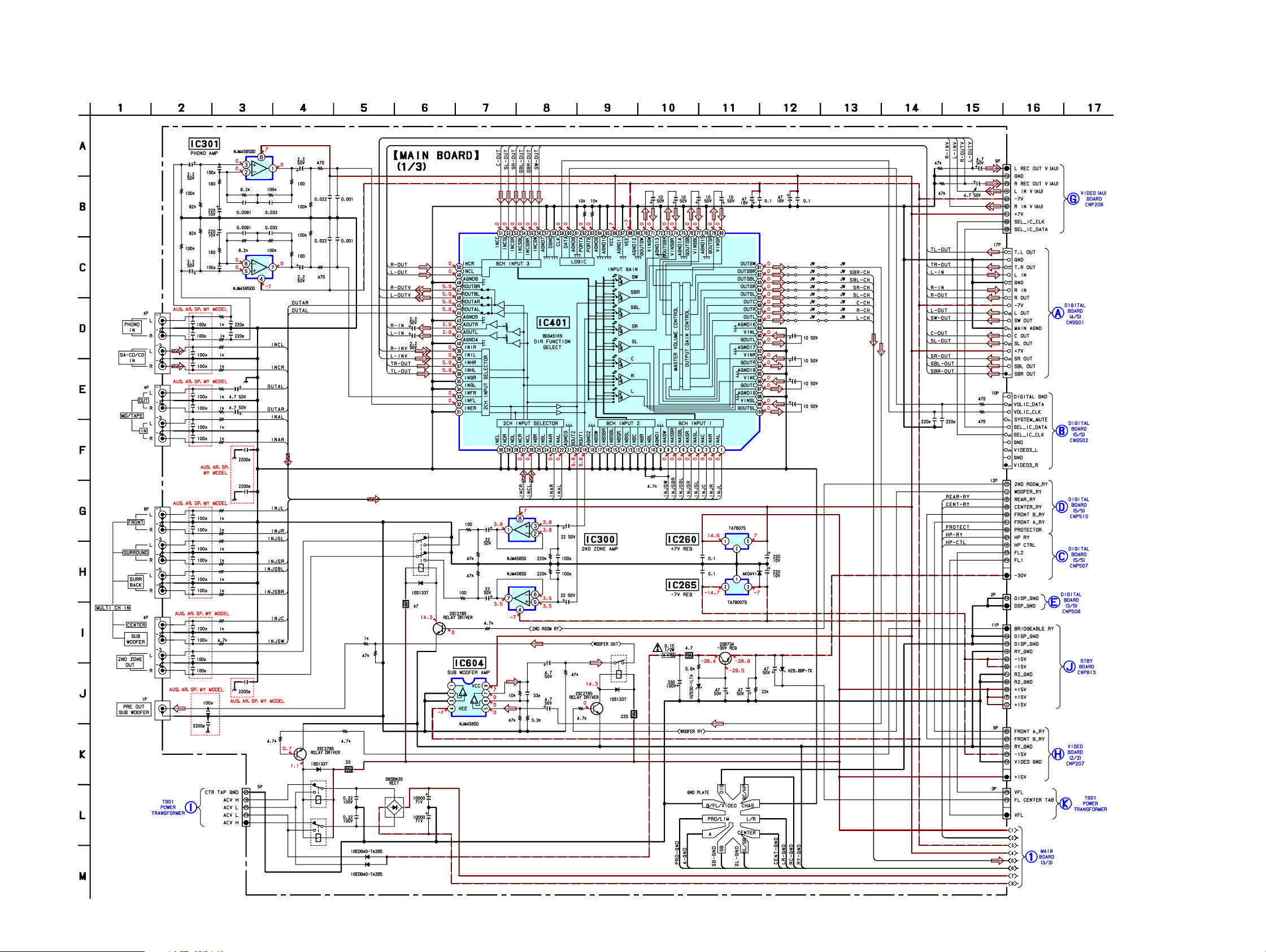
4-9. SCHEMATIC DIAGRAM — MAIN SECTION (1/3) —
STR-DE898/DE998
J301
J302
C303
R302
R352
C353
R303
R353
C301
C351
CC01
CC02
CC363
CC313
CC364
CC314
C305
C355
R304
C304
C354
R354
R301
R351
R311
R361
R363
R313
R364
R314
IC301(1/2)
R305 R306
C356 C357
R355 R356
IC301(2/2)
C302
C352
C363
C313
C341
C308
R309
R307
C309 C310
R308
C307C306
R358
C359 C360
R357
C358
R359
C486
C485
R656 R658
IC401
C390 C840 C490
C690
C417
C418
C429
C394
C844
C494
C694
C644
C444
C544
C594
C428
C590
C540
C440
C640
R395
R795
R495
R695
R645
R445
R545
R595
R440
R441
C478
CNP812
C479
(Page 36)
CNP811
(Page 31)
CNP814
R408
C408C409
R409
(Page 32)
J305
J306
J304
CC401
CC451
CC501
CC551
CC601
CC651
CC701
CC751
C333
C383
C345
CC374
R401
R451
R501
R551
R601
R651
R701
R751
C343
C344
CN908
R824
D818
RY803
Q809
R825
R830
C802
R388
R389
D801
R342
RY300
D300
C803
Q300
R382
R332
IC604
R331
R381
C332
C382
R341
IC300(1/2)
IC300(2/2)
R390
R391
R330
R380 C381
C395
C392
C391
R392
C331
C330
C380
R396
R397
Q351
RY351
D351
R398
R752
R290
C290
R250
R251
D250
GP1
C260
C265
Q250
C250 C251
IC260
IC265
D265
C252
R252
C261
C266
D251
CN507
CNP805
CNP804
CN803
CNP802
(Page 32)
(Page 32)
(Page 30)
(Page 45)
(Page 40)
STR-DE898/DE998
(Page 45)
RY802
C800
D290
D291
C804
(Page 45)
(Page 25)
23 23
Page 24
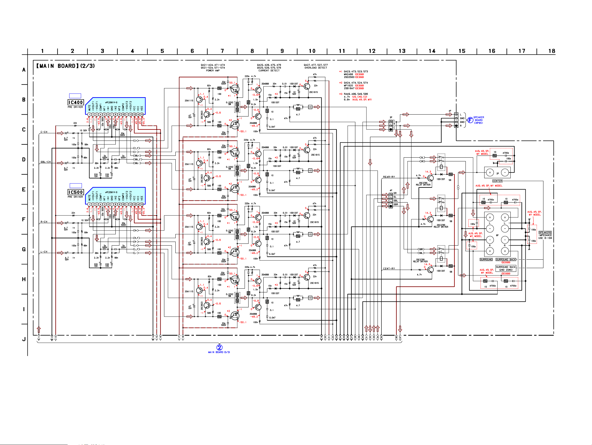
STR-DE898/DE998
4-10. SCHEMATIC DIAGRAM — MAIN SECTION (2/3) —
C411
C461
C511
C561
IC B/D
R400
R411
C412
C462
R461
IC B/D
R500
R511
C512
C562
R561
C403
R412
R462
C503
R512
R562
C414
C415 C465
R415
R416
R466
C416 C466
C514
C515 C565
R515
R516
R566
C516 C566
IC400
IC500
C413
C513
C463
R465
C563
R565
C464
C564
• See page 52 for IC Block Diagrams.
C425
C423
R421
R423
Q423
Q422
Q472
Q522
Q572
R424
R471
R474
R521
R524
R571
R574
R422
R472
R522
R572
R425
R473
R475
R523
R525
R573
R575
R428
Q424
C424
C475
C473
Q473
R478
Q474
C474
C525
C523
Q523
R528
Q524
C524
C578
C573
Q573
R578
Q574
C575
Q421
C421
Q471
C471
Q521
C521
Q571
C571
R477
Q476
Q526
R577
R427
R426
Q426
R476
R527
R526
R576
Q576
R429
R430
R479
R480
R529
R530
R579
R580
Q425
Q475
Q575
R433
R483
R533
R583
R431
C431
C432
R481
C481
C482
R531
C531
C532
R581
C581
C582
R432
D426
R482
D526
D576
R446
R496
R532Q525
R546
R582
R596
D476
C426
C476
C526
C576
R434
R437
R484
R487
R534
R537
R584
R587
D425
C427
D475
C477
D525
C527
D575
C577
L401
R439
L451
R489
L501
R539
L551
R589
CN400
CN450
CN500
CN550
Q427
R435
R485
R486
Q477
R535
R536
Q527
R585
R586
Q577
R436
CN301
CN300
R605
Q700
R705
Q600
R405
RY600
D600
RY400
D400
Q400
RY700
D700
CN851
R606
R406
R706
(Page 34)
RR11 RR61
C700
C600
RR81
CC81
C750
TM601
TM602
CC21 CC71
RR71RR21
CC61CC11
C400
C300
STR-DE898/DE998
(Page 25)
2424
Page 25
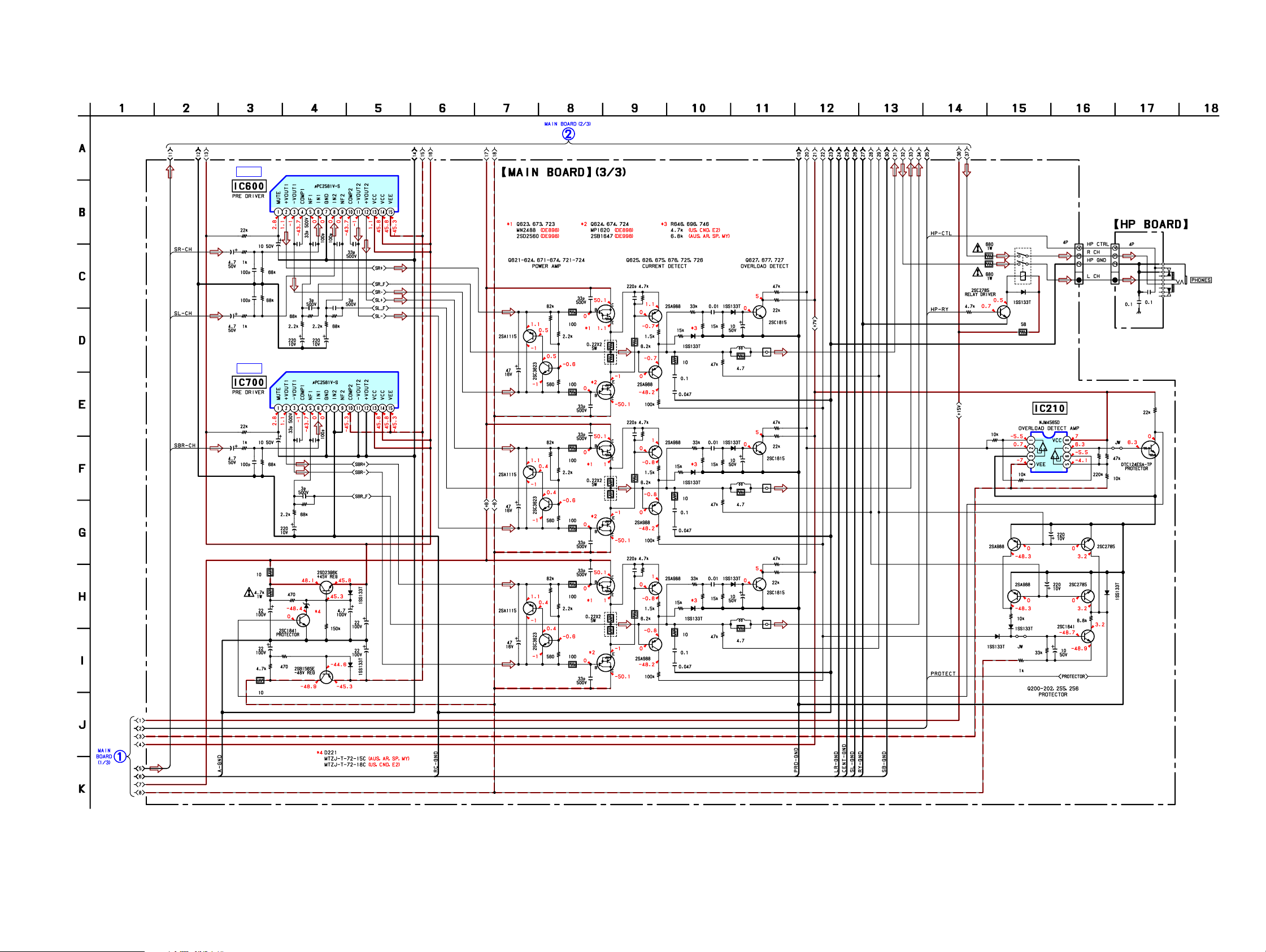
STR-DE898/DE998
4-11. SCHEMATIC DIAGRAM — MAIN SECTION (3/3) —
C611
C661
C711
IC B/D
R600
R611
C612
C662
R661
IC B/D
R700
R711
C712
R220
R221
C220
C230
R233
R234
C603
R612
R662
C703
R712
R716
C716
Q225
R235
C614
C615 C665
R615
R616
R666
C616 C666
C714
C715
R715
R222
D221
Q235
IC600
IC700
Q220
C613
C713
R236
R665
C663
C233
C664
D220
C221
C231
D235
• See page 52 for IC Block Diagrams.
R621
Q621
C621
Q622
R624
R671
Q671
C671
Q672
R674
R721
Q721
C721
Q722
R724
R622
R672
R722
R623
R625
R673
R675
R723
R725
(Page 24)
C623
Q623
C624
C673
Q673
C674
C723
Q723
Q724
C724
R628
Q624
R678
Q674
R728
C625
C675
Q676
Q726
R627
R677
R727C725
Q626
R626
R676
R726
R629
R630
R679
R680
R729
R730
Q625
Q675
Q725
R683
R733
R633
C631
C681
C731
R631
C632
R681
C682
R731
C732
D626
D676
R632
R646
R696
R746
D726
R732
R682
C626
C676
C726
R634
R637
R684
R687
R734
R737
D625
D675
D725
C627
C677
C727
L601
R639
L651
R689
L701
R739
CN600
CN650
CN700
Q677
R736
Q727
R635
R636
R685
R686
R735
Q627
R245
Q240
R240
RY240
R280
D240
R246
R210
R211 R212
Q255
Q200
R201
D202
D203 R202
R204
R203
IC210
C200
C255
CN806
Q202
C201
Q201
R205
Q256
R213
R214
D210
D201
CNP701
C2502
J2501
C2501
TP700
R215
Q210
(Page 23)
STR-DE898/DE998
25 25
Page 26
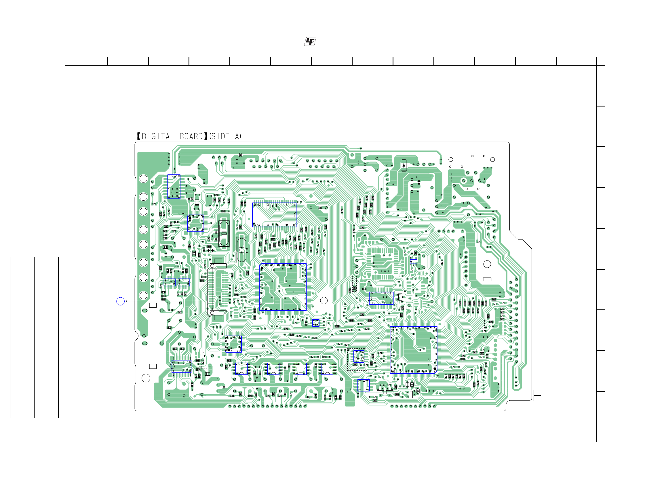
STR-DE898/DE998
4-12. PRINTED WIRING BOARD — DIGITAL SECTION (SIDE A) —
IC1302
• Semiconductor
Location (Side A)
Ref. No. Location
D1001 C-5
D1103 H-5
D1105 H-5
D1106 H-5
D1301 E-10
D2702 F-5
IC1101 H-5
IC1111 E-5
IC1131 H-6
(IC1141) H-6
IC1301 D-10
IC1302 C-11
IC1303 F-11
IC1373 F-11
IC1401 H-11
IC1403 H-9
IC1404 H-8
IC1405 H-8
IC1406 H-7
IC1452 G-9
IC1501 F-8
IC1502 D-8
IC1503 G-7
IC2102 F-6
Q1103 I-6
Q1104 I-6
Q1105 I-5
AV SYNC JRC
BOARD
CN7001
(Page 33)
R1351
R1303
C1303
C1304
R1357
L
R1356
R1352
C1302
FB1306
R1354
R1358
C1357
R1353
R1304
JR1301
C1360
IC1303
C1361
C1375
C1405
R1362
C1301
R1301
R1359
R1377
C1377
R1376
IC1401
• See page 14 for Circuit Boards Location. : Uses unleaded solder.
C1258
R1316
C1313
R1310
30 15
16 1
R1313
R1311
C1310
C1309
CNS551
R1315
IC1452
R1484
R1480
C1002
C1287
R1312
R1516
X1301
R1504
R1502
JR1953
IC1403
R1555
R1505
R1506
R1556
R1486
R1541
R1501
R1507
R1446
R1520
X1502
R1523
JR1951
C1441
R1522
R1521
JR1952
C1247
R1519
C1471
R1476
IC1502
C1519
R1517
R1554
R1518
IC1404
R1553
R1552
IC1501
C1277
R1436
R1526
R1525
R1508
R1551
R1510
R1151
C1431
C1237
R1550
R1549
IC1405
C1421
R1426
R1548
R1547
R1153
R1544
R1546
R1527
R1528
R1152
C1267
R1543
R1545
C1502
R1154
R1410
C1516
R1539
R1540
R1542
C1411
R1535
R1538
R1450
R1466
R1536
R1537
IC1503
IC1406
R1416
R1532
R1533
R1534
C1217
R1041
R1160
R1140
C1257
R1134
R1042
R1161
R1456
C1380
IC1373
C1408
C1315
IC1301
FB1303
FB1304
R1379
R1321
R1378
R1404
FB1405
C1409
JR1300
R1318
R1309
R1360
R1308
R1306
R1305
R1322
EXCEPT
SP,MY MODEL
FB1452
R1403
R1407
D1301
R1405
R1086
R1121
R1138
DE998
R1139
R1144
R1149
EXCEPT
DE898:US,CND
MODEL
IC1141
R1165
R1066
R1065
C2102
R1137
R1164
IC1131
R1068
R1085
R1142
R1044
R1084
R1119
R1067
R1162
R1049
R1120
R1117
R1118
R1087
IC2102
R1156
R1163
R1178
Q1103
R1177
Q1104
R1099
D1001
R1128
AKA
R1123
R1176
D2702
R1058
IC1101
D1103
Q1105
R1127
R1189
C1137
IC1111
D1106
C1021
D1105
R1101
R1095
R1196
R1021
R1141
R1092
R1093
C1119
R1116
R1115
R1091
R1199
R1114
R1113
R1195
R1187
R1083
R1112
R1037
R1102
R1109
R1111
R1110
R1194
R1132
R1057
R1103
R1107
R1108
R1192
R1193
R1131
R1022
R1186
R1191
R1172
R1173
R1174
DE998
JR1102
R1023
R1105
R1088
1-865-763-
2345678910111213
11
(11)
1
A
B
C
D
E
F
G
H
I
( ): Except STR-DE898: US, CND model
STR-DE898/DE998
2626
Page 27

STR-DE898/DE998
4-13. PRINTED WIRING BOARD — DIGITAL SECTION (SIDE B) —
1
234567891011
A
(Page 22)
B
CNS503
R1096
R1180
DE998
R1184
FB1076
C1905
42
C1032
R1097
C1097
CNP510
R1179
C1142
R1129
C1129
FB1075
FB1078
135
7
1
C1254
R1200
C1133
C1124
FB1077
C1906
1
D1107
D1110
C1101
C1134
C1136
C1123
C1122
R1185
CNP507
C1256
C1255
C1131
C1132
R1063
D1111
R1126
C1130
C1135
R1064
C1012
C1031
5
R1035
C1102
D1108
C1106
C1110
R1124
C
D
E
F
G
H
D
MAIN
BOARD
CN507
(Page 22)
CNP507
DISPLAY
(Page 42)
BOARD
CN507
GRY
GRY
GRY
GRY
GRY
GRY
RED
BOARD
CNS101
MAIN
C
RED
CNP510
O
(Page 22)
GRY
7
1
GRY
GRY
IC1901
C1908
GRY
FLASH
PROGRAMMING
R1181
R1182
CNS505
R1183
I
• See page 14 for Circuit Boards Location. : Uses unleaded solder.
MAIN
BOARD
CNP805
C1011
1
2
3
C1100
R1089
EXCEPT
US,CND
MODEL
C1127
IC1011
23
IC1031
R1201
C1103
R1094
DE998
R1098
E
1
C1022
C1104
C1105
R1190
R1198
IC1021
R1252
R1251
C1107
X1101
R1169
C1121
CNS502
1
2
3
C1108
R1125
C1126
C1109
R1060
C1120
BLU
BLU
R1166
CNP506
10
5
2
1
10
CNP506
C1099
FB1101
R1136
R1061
R1167
R1168
4
3
1
FB2035
R2346
R1170
R1155
R1157
R1054
GRY
GRY
GRY
GRY
RED
GRY
GRY
RED
C1139
C1913
C1459
R1159
R1090
R1106
R1071
R1072
IC1902
DE898:
US,CND
MODEL
R1158
P
1
2
3
R1073
STBY
BOARD
CNP810
(Page 44)
C1914
R1146
C1006
R1145
R1143
EXCEPT
DE898:US,CND
MODEL
R1133
C1140
C1453
C1488
R1511
R1454
(Page 38)
CNP504
FB1502
C1515
R1573
R1574
R1150
C1451
C1478
VIDEO
BOARD
CNP210
FB1501
R1571
R1570
C1517
C1005
R1414
C1413
C1458
C1504
R1460
C1463
JR1213
C1513
R1572
C1507
FB1102
R1424
C1461
R1464
C1418
C1518
C1508
C1505
C1514
R1420
R1434
C1227
C1520
R1509
R1430
C1423
C1433
C1428
TN1
CNS508
R1514
C1501
C1509
R1474
C1468
BA
MAIN BOARD
CNP814
(Page 22) (Page 22)
MAIN BOARD
CNP811
C1252
C1510
R1513
C1503
C1491
R1470
C1473
CNS501
C1251
C1253
R1512
R1560
FB1504
R1444
C1443
C1438
C1521
C1522
R1503
C1511
JR1216
R1440
R1261
C1481
C1448
FB1503
FB1505
R1471
(Page 41)
S-VIDEO
BOARD
CNS204
CNS509
R1260
C1450
C1483
3
2
1
NM
C1316
R1314
C1457
C1494
IC1001
FB1309
C1141
C1312
R1320
C1460
C1001
C1317
C1314
C1308
FB1305
FB1453
C1403
C1454
C1004
C1306
D1004
R1302
D1003
C1401
C1404
C1406
C1370
C1402
C1359
C1355
C1381
FB1302
C1305
C1407
C1358
C1351
C1352
C1353
C1354
C1356
3
2
1
3
2
1
3
2
1
3
2
1
R1355
R1366
1-865-763-
12 13
IC1351
TV/SAT
IN
IC1352
IC1353
IC1354
-1
C1362
-2
11
(11)
ASSIGNABLE
(INPUT ONLY)
J1301
• Semiconductor
Location (Side B)
Ref. No. Location
D1003 F-10
D1004 F-10
D1107 E-4
D1108 E-4
D1110 F-4
D1111 F-4
IC1001 H-10
IC1011 C-5
IC1021 C-5
IC1031 D-4
IC1351 C-12
IC1352 D-12
IC1353 E-12
IC1354 F-12
IC1901 C-4
IC1902 C-6
STR-DE898/DE998
27 27
Page 28

STR-DE898/DE998
4-14. SCHEMATIC DIAGRAM — DIGITAL SECTION (1/5) —
IC1351
IC1352
IC1353
IC1354
J1301
C1356
C1362
R1366
R1355
R1351
R1352
C1353
R1353
R1354
C1361
C1355
C1351
C1352
C1354
C1381
R1376 R1377 R1378
C1375
C1377
IC1373 IC1303
• See page 48, 51 for IC Block Diagrams. • See page 21 for Waveforms.
FB1302
IC B/D
R1379
C1380
C1370
R1356
C1357
C1141
IC1302
R1357
R1358
R1359
C1360
R1362
FB1306
JR1301
C1359
C1358
FB1309
C1316
C1317
C1302
R1303
C1303
C1304
C1301
R1301
C1306
JR1300
R1302
R1304
C1305
C1315
IC B/D
R1318
FB1303
1360
R
C1314
4
TP100
IC1301
8
C130
C1309
TP1003
R1310
X1301
C1310
R1316
C1313
R1311
R1314
C1312
(Page 30)
R1315
R1313
R1312
(Page 32)
(Page 31)
(Page 29)
R1305
FB1304
R1308
FB1305
D1301
R1309
STR-DE898/DE998
2828
Page 29

STR-DE898/DE998
4-15. SCHEMATIC DIAGRAM — DIGITAL SECTION (2/5) —
R1512
R1516
C1522C1521
R1523
JR1951
JR1952
JR1953
R1556
R1306
FB1503
R1502
R1503
R1504
R1505
R1506
R1507
FB1504
X1502
R1513
C1501
• See page 21 for Waveforms. • See page 53 for IC Pin Function Description.
(Page 28)
C1511
C1503
R1501
TP1005
C1509
R1514
C1514
R1520
C1510
R1521
R1522
R1519
R1518
IC1501
R1517
R1554
R1553
R1552
C1513
R1525
R1526
R1551
R1550
R1549
R1548
R1547
R1546
C1508
C1507
R1574
R1573
R1572
R1571
R1570
R1528
R1527
R1544
R1545
R1543
R1542
R1540
R1539
R1538
R1537
R1536
R1535
R1511
R1534
R1533
R1532
IC1502
C1517
C1518 C1516
IC1503
(Page 30)
C1519C1520
C1515
FB1502
FB1501
(Page 32)
(Page 31)
R1560
FB1505
R1508 R1509
TP1008
TP1009
TP1010
TP1011
R1541
R1555
TP1012
TP1013
TP1014
TP1015
R1510
C1502
C1504
C1505
STR-DE898/DE998
29 29
Page 30

STR-DE898/DE998
4-16. SCHEMATIC DIAGRAM — DIGITAL SECTION (3/5) —
(Page 28)
(Page 29)
FB2035
C1104
C1106
R1126
IC1111
IC1011 IC1021
D1001
CNP506
(Page 31)
C2102
IC2102
R2346
D2702
C1137
R1127
(Page 32)
R1189
C1107
C1011
C1031
C1012 C1022
IC1031
C1032
C1021
C1908
C1099
(Page 45)
IC1901
C1905
(Page 23)
C1906
STR-DE898/DE998
3030
Page 31

STR-DE898/DE998
4-17. SCHEMATIC DIAGRAM — DIGITAL SECTION (4/5) —
CNS551
R1320
R1321
R1322
(Page 33)
• See page 50, 51 for IC Block Diagrams. • See page 21 for Waveforms.
(Page 29)
(Page 28)
(Page 30)
(Page 32)
(Page 23)
TN1
IC B/D
CNS508
CNS501
C1252
C1253
R1260 R1261
R1251
R1252
C1251
C1258
TP1016
C1006
C1004
C1914
IC1902
D1003
C1247
C1277
C1237
C1267
C1227
C1913
R1486
R1446
R1476
R1436
R1466
R1426
D1004
C1448C1287
C1438
C1468
C1428
C1458
C1418
C1005
R1404
R1405
FB1405
C1404
C1403
C1408
C1405
C1401
C1402
C1483
C1481
R1480
IC1401
R1484
C1409
R1403
R1444
R1407
R1440
C1406
C1407
FB1452
C1443
C1441
C1473
C1471
C1450
C1454
FB1453
R1470
R1474
R1471
C1494C1460
C1457
R1430
R1434
C1431
IC1452
C1463C1433
C1461
R1460
R1464
IC B/D
R1424
C1491
R1420
C1423
C1421
C1453
C1451
R1450
C1001
R1454
IC1001
C1002
R1410
IC1406IC1405IC1404IC1403
R1414
C1413
C1411
STR-DE898/DE998
C1257
C1217 C1478
R1456
R1416
C1488
31 31
Page 32

STR-DE898/DE998
4-18. SCHEMATIC DIAGRAM — DIGITAL SECTION (5/5) —
(Page 28)
(Page 29)
• See page 21 for Waveforms. • See page 55 for IC Pin Function Description.
(Page 30)
R1037
R1066
X1101
R1067
C1108
R1137
R1125
R1136
C1109
R1134
R1139
C1105
R1170
R1123
R1124
R1129
R1058
R1128
R1190
C1102
C1103
R1090
TP1018
R1201
C1100
TP1017
R1121
R1085
R1086
R1084
R1089
R1035
R1101
R1087
R1065
R1187
C1097
FB1101
R1179
R1180
R1181
R1182
R1088
JR1102
CNS509
(Page 41)
CNP507
(Page 23)
CNS505
(Page 31)
FB1102
IC1141
C1459
R1138
R1163 R1164
C1139
C1140
R1165
IC1131
R1159
R1150
R1142
R1143
R1144
R1149
R1044
R1041
R1042
C1120
R1140
R1145
R1146
R1151
R1153
R1152
R1154
R1155
R1156
R1160
R1161
R1162
Q1105
R1099
R1071
R1157
R1158
R1072
R1073
R1098
R1060
R1061
D1105
R1054
R1133
R1063
R1064
R1167
R1168
R1169
D1103
D1106
R1120
R1185
R1049
IC1101
C1121
C1127
R1094
R1091
R1198
R1199
R1093
R1092
R1141
C1119
R1172
C1124
R1173
C1123
R1174
C1122
C1255
C1142
C1110
R1022
C1256
C1254
R1068
R1119
R1118
R1117
R1116
R1115
R1114
R1113
R1200
C1129
C1130
C1131
C1132
C1133
C1134
C1135
C1136 R1196
R1102
R1103
R1021
R1023
Q1103
C1101
R1106
R1083
R1112
R1111
R1110
R1109
R1108
R1107
R1186
R1105
R1191
R1192
R1193
R1194
R1195
R1057
R1166
R1095
Q1104
R1177
R1176
C1126
D1108
D1107
D1111
D1110
R1096 R1097
FB1075
FB1078
FB1077
FB1076
R1132
R1131
R1184
R1183
(Page 43)
CNP510
(Page 23)
CNS503
CNS502
(Page 23)
CNP504
STR-DE898/DE998
R1178
(Page 39)
3232
Page 33

STR-DE898/DE998
4-19. PRINTED WIRING BOARDS — AV SYNC JRC SECTION —
1
234567891011
A
R7002
B
C
C7004
IC7001
C7005
C7002
C7003
FB7001
IC7002
R7003
30
C7001
16
D
• See page 14 for Circuit Boards Location. : Uses unleaded solder.
15
DIGITAL
BOARD
L
CN7001
1
1-866-385-
11
(11)
CNS551
(Page 26)
1-866-385-
11
(11)
4-20. SCHEMATIC DIAGRAM — AV SYNC JRC SECTION —
R7003
IC7002
C7005
R7002
C7004C7003
C7002
C7001
FB7001
IC B/D
IC7001
• See page 50 for IC Block Diagrams.
CN7001
(Page 31)
STR-DE898/DE998
33 33
Page 34

STR-DE898/DE998
4-21. PRINTED WIRING BOARD — SPEAKER SECTION —
1
A
23456
TM2880
SPEAKERS
IMPEDANCE USE 8-16Ω
R
R
B
C2870
2810
JW
101
RR
CC101
R2873
1
RY
4
R2871
Q2880
CNP852
RR
Q2881
102
JW
JW
JW
2806
2807
2808
JW
JW
C2850
CC102
2811
2805
D2881
RY2881
C2880
C2860
R2872
AUS,AR,SP,M
M
R2870
JW2813
D2880
2804
JW
1
RED
C
D
VIDEO
ARD
BO
CN206
(Page 38)
AUS,AR
SP,M
M
Q
,
Y
DEL
O
RED
G
GRY
GRY
• See page 14 for Circuit Boards Location. : Uses unleaded solder.
CC104
ODEL
L
L
RR104
Y
RY2880
P851
CN
BLK
BLK
4
RED
JW2803
JW2802
FRONT A
FRONT B
RR
JW2801
JW2800
103
AUS,AR,
Y
SP,M
EL
OD
M
CC103
1-865-748-
11
(11)
AIN BOARD
M
(Page 22)
4-22. SCHEMATIC DIAGRAM — SPEAKER SECTION —
RY2881
D2881
R2872
RY2880
(Page 24)
D2880
CNP852
R2870
Q2881
F
CN851
Q2880
R2873CNP851
R2871
RR102
RR101
CC102
CC101
C2870
C2850
TM2880
C2860
C2880
(Page 40)
STR-DE898/DE998
RR104
RR103
CC104
CC103
3434
Page 35

STR-DE898/DE998
4-23. PRINTED WIRING BOARDS — VIDEO (AU) SECTION —
1
A
23456789
J2552
TV/SAT
AUDIO IN
-1
L
-2
R
DVD
AUDIO IN
-3
L
AUDIO OUT
-5
L
-4
R
-6
R
B
C
D
E
AUS,AR,
SP,MY
MODEL
CC112
R2553
R2556
JW
JW2551
9
GRY
2554
GRY
R2555
JW2552
CNP208
GRY
BLU
C2552
CC111
JW
JW2553
GRY
R2552
GRY
2555
GRY
GRY
R2558
1
CC114
R2559
BLU
CC113
R2557
C2555
R2580
R2577
R2578
R2554
CC116
R2563
R2562
R2582
JW2559
JW2560
2561
JW
CC115
R2561
C2554
JW2562
R2579
R2581
JW2563
• See page 14 for Circuit Boards Location. : Uses unleaded solder.
J2553
L
CC119
R2571
R2572
IC2560
-4
R
C2556
VIDEO 1
R2568
JW
JW
CC122
R2574
2569
2568
AUDIO IN
-5
L
CC121
R2575
2572
JW
2571
JW
JW2570
-6
R
R2573
CNP209
1
HT
W
R2570
3
BLK
PNK
1-865-766-
11
(11)
VIDEO 2
R2560
AUDIO IN
-1
L
CC118
R2565
JW2565
JW2564
-2
R
CC117
R2566
R2567
JWH2566
C2566
C2557
JW2567
C2559
R2569
R2564
AUDIO OUT
-3
CC120
C2565
F
G
H
AIN
M
BOARD
G
CNP812
(Page 22)
TP201
BLK
(CHASSIS)
I
C2051
15
CN299
HT
YEL
BLK
W
(Page 41)
R
S-VIDEO
BOARD
CNP205
(DE898)
BLK
PNK
C2052
J2052
C2057
C2058
1-865-750-
11
(11)
TP202
C2701
J2702
G
G
Y
-4
S-VIDEO
1
HT
W
S
S-VIDEO
BOARD
CNP205
(DE998)
CN209
YEL
PNK
(Page 41)
BLK
HT
BLK
W
C
C2702
7
1-865-749-
PNK
BLK
(CHASSIS)
11
(11)
STR-DE898/DE998
35 35
Page 36

STR-DE898/DE998
4-24. SCHEMATIC DIAGRAM — VIDEO (AU) SECTION —
C2552
J2552
J2553
CC111
CC112
CC113
CC114
CC115
CC116
CC117
CC118
CC119
CC120
R2552
R2553
R2554
R2560
R2559
R2563
R2564
R2568
R2565
R2569
R2555
R2556
R2557
R2558
R2561
R2562
R2566
R2567
R2571
R2572
C2554
C2555
C2556
C2557
• See page 46 for IC Block Diagrams.
C2566C2565
IC2560
R2581
R2582
R2577
R2578
R2579
R2580
CNP208
(Page 23)
CNP209
J2052
C2057
CC121
CC122
C2058
TP201
R2570
R2575
C2051C2052
R2573
R2574
C2559
CN299
(Page 41)
IC B/D
J2702
CN209
(Page 41)
C2702 C2701
STR-DE898/DE998
TP202
3636
Page 37

STR-DE898/DE998
4-25. PRINTED WIRING BOARD — VIDEO SECTION (SIDE A) —
D3254
D3253
Q3252
R3277
R3278
D3301
R3304
Q3301
R3323
IC3321
R3324
R3305
FB3252
R3322
R3302
TP3003
TP3001
C2338
Q3304
R3307
R3316
R3315
D3302
Q3302
R3306
• See page 14 for Circuit Boards Location. : Uses unleaded solder.
R3275
FB3701
R3276
C3602
R3603
C3604
C3276
FB3601
FB3602
R3321
C3721
EXCEPT
US,CND MODEL
C3607
R3636
R3638
IC3721
R3604
C3605
R3637
R3213
R3632
R3631
R3633
R3630
IC3601
C3608
C3609
Q3632
C3631
R3635
US,CND
MODEL
C3601
C3611
R3621
R3634
IC3701
R3622
Q3631
Q3622
R3628
R3711
Q3621
R3626
C3718
R3710
R3701
EXCEPT
US,CND
MODEL
R3605
R3625
C3621
R3627
R3702
C3615
R3606
C3613
R3623
C3715
R3703
R3607
C3614
R3624
R3709
R3707
R3705
C3710
R3658
R3659
Q3653
Q3652
R3656
Q3651
R3651
R3708
R3619
Q3604
IC3671
Q3674
FB3662
R3655
FB3603
R3653
R3652
IC3741
R3741
R3611
R3612
Q3601
R3657
R3654
R3670
Q3677
R3681
R3679
R3690
R3678
Q3673
R3677
R3751
IC3751
Q3678
R3731
Q3503
R3689
R3682
Q3675
R3683
C3751
R3672
R3687
D3601
R3732
R3503
R3501
R3686
R3684
FB3703
Q3676
R3735
C3734
R3502
Q3502
R3211
R3688
IC3651
R3733
C3205
R3801
D3732
D3733
D3731
C3510
FB3501
R3209
R3734
Q3731
IC3201
IC3501
C3511
C3653
R3513
C3503
R3507
C3505
R3508
R3514
R3515
L3501
C3501
C3502
DE998
R3802
R3803
R3512
R3511
R3510
R3201
R3506
R3516
R3504
R3517
R3505
R3518
EXCEPT
US,CND
MODEL
1-865-764-
R3203
R3202
TP3002
23456789101112
EXCEPT
DE898:US,CND
R3204
MODEL
US,CND
MODEL
11
(11)
1
A
B
C
D
E
F
G
H
• Semiconductor Location (Side A)
Ref. No. Location
D3253 C-8
D3254 C-9
D3301 D-9
D3302 E-9
D3601 E-5
D3731 E-4
D3732 E-4
D3733 E-4
IC3201 C-4
IC3321 E-9
(IC3501) F-4
IC3601 D-7
IC3651 D-4
IC3671 C-6
IC3701 G-7
<IC3721> G-8
IC3741 G-6
IC3751 F-5
Q3252 C-9
( ): STR-DE998
< >: Except US, CND model
Ref. No. Location
Q3301 E-9
Q3302 E-9
Q3304 E-9
(Q3502) H-4
(Q3503) G-5
Q3601 E-5
Q3604 E-6
Q3621 E-7
Q3622 F-7
Q3631 E-7
Q3632 E-7
Q3651 E-6
Q3652 E-6
Q3653 E-6
Q3673 D-5
Q3674 D-6
Q3675 D-5
Q3676 D-5
Q3677 D-5
Q3678 C-5
Q3731 F-4
STR-DE898/DE998
I
37 37
Page 38

STR-DE898/DE998
4-26. PRINTED WIRING BOARD — VIDEO SECTION (SIDE B) —
1
23456789101112
A
TV/SAT
J3101 J3102
B
R3207
C3207
C3216
C3208 C3210
R3208
C3209
C
D3201
D
E
C3214
R3214
DE998
C3201
C3507
D3202
C3202
C3508
C3504
C3206
C3651
D3602
C3652
C3733
F
C3514
CNS201
C3506
C3512
X3501
T
Q3501
B C E
S-VIDEO
BOARD
CNS202
(Page 41)
G
H
4
(TEST)
DIGITAL
BOARD
CNP504
(Page 27)
M
TP3002
CNP3501
1
CNP210
CT3502
I
C3215
C3732
IC3731
C3513
• See page 14 for Circuit Boards Location. : Uses unleaded solder.
J3103
C3213
C3610
FL3631
C3722
X3701
R3404
C3818
C3603
C3612
C3616
C3633
C3711
C3702
C3706
C3705
C3704
C3703
EXCEPT US,CND
MODEL
BOARD
(Page 22)
C3606
C3712
AIN
M
CN803
C3275
C3279
C3278
IC3253
15
C3277
C3321
C3322
C3632
C3323
C3324
C3701
C2337
1
2
IC3103
3
CNP207
16
GRY
GRY
GRY
RED
H
C3671
C3679
Q3671
C3673
R3671
R3680
R3673
C3731
15
C3753
C3744
R3210
R3676
Q3672
R3685
C3672
C3743
R3675
R3610
C3745
R3674
C3741
C3746
C3678
FB3661
C3752
C3677
C3676
C3674
C3641
R3706
C3211
C3648
C3716
R3717
C3675
C3646
C3717
C3714
C3709
C3217
C3713
C3622
C3623
X3703
R3714
C3212
R3713
R3704
X3702
C3719
C3720
C3708
US,CND
MODEL
R3212
FL3621
R3712
Q3701
C3707
C2335
GRY
C3325
3
2
1
GRY
RY3304
R2331
IC3104
TV/SAT
IN
-2
C2336
C2339
(ASSIGNABLE)
-1
-3
C3255
RY3303
R3303
C2377
3
2
IC3101
1
C2340
J3104
COMPONENT VIDEO
DVD
IN
-4
-5
-6
R3301
C2379
CN206 CN206
1
1
2
IC3102
3
4
1-865-764-
TP3003
TP3001
MONITOR
OUT
-8
JR2330
RY3301RY3302
11
(11)
-7
Y
P
B/CB
/B-Y
R/CR
P
-9
/R-Y
• Semiconductor
Location (Side B)
Ref. No. Location
D3201 D-3
D3202 D-3
D3602 E-4
IC3101 F-10
IC3102 G-10
IC3103 G-9
IC3104 G-9
IC3253 D-8
IC3731 F-5
(Q3501) G-4
Q3671 D-5
Q3672 D-5
Q3701 G-7
Q
SPEAKER
BOARD
CNP852
(Page 34)
RED
1
GRY
GRY
GRY
4
( ): STR-DE998
STR-DE898/DE998
3838
Page 39

STR-DE898/DE998
4-27. SCHEMATIC DIAGRAM — VIDEO SECTION (1/2) —
J3101
J3102
J3103
R3207
R3208
C3209
R3210
C3211
R3212
C3213
R3209
C3210
R3211
C3212
R3404
C3217
C3207
C3216
C3208
C3215
R3213
IC B/D
IC3201
C3206
R3214
C3214
C3205
• See page 47, 48, 49, 51 for IC Block Diagrams. • See page 21 for Waveforms.
IC3501
R3507
D3202
C3201
R3201
D3201
R3203
R3204
R3202
C3202
R3501
Q3502
R3502
Q3501
Q3503
R3503
CT3502
R3503
IC B/D
C3510
C3512
C3513
C3514
C3511
TP3502
X3501
R3508
FB3501
C3508C3507
L3501
C3506
C3505
C3504
C3503
C3502
C3501
R3513
R3515
R3514
R3510
R3511R3512
R3506
R3504
R3505
CNP3501
CNP210
(Page 32)
R3672
R3671
R3673
Q3671
C3678 C3679
FB3661
FB3662
R3674
C3671
R3675
IC B/D
C3675
C3676
R3677
Q3672
R3676
IC3671
R3679
R3678
Q3673
R3681
C3672
R3690
C3674
R3683
Q3674
R3682
C3677
R3670
R3680
R3685 R3687
R3684
C3673
R3686
Q3675
R3689
Q3678
Q3677
D3602
R3688
Q3676
C3651
C3652
C3653
R3801
R3802
IC3651
IC B/D
R3803
FB3603
R3651
R3653
Q3651
R3652
R3610
C3646
R3656
R3654
Q3653
Q3652R3655
R3657
Q3601
C3648
R3612
R3611
CNS201
(Page 41)
R3659
R3658
Q3604
R3619
STR-DE898/DE998
(Page 40)
39 39
Page 40

STR-DE898/DE998
4-28. SCHEMATIC DIAGRAM — VIDEO SECTION (2/2) —
IC B/D
IC3253
C3279
R3277R3278
C3278
R3276
C3277
R3301
D3253
C3276
D3254
C3275
• See page 46, 47, 49, 51, 52 for IC Block Diagrams. • See page 21 for Waveforms.
Q3252
R3275
FB3252
R3630
R3638
C3633
Q3632
R3628
C3623
Q3622
C3745 C3744 C3743
C3746
R3635
R3636
C3632
R3637
R3625
R3626
C3622
R3627
R3741
IC B/D IC B/D
IC3741 IC3751
FL3631
FL3621
C3631
R3634
C3621
R3624
C3753
C3751
C3752
R3633
R3623
R3632
R3622
R3631
Q3631
R3621
Q3621
(Page 39)
FB3602
C3607
C3612
C3611
C3608
C3616
C3609
C3610
R3605
R3606
C3613
C3606
C3605
R3607
C3603
C3614
C3604
C3615
R3604
IC3601
R3603
C3602
FB3601
IC B/D
IC3103 IC3102
C3818
C3601
R3518
C3641
R3516
R3517
J3104
C3255
JR2330
RY3301
RY3302
RY3303
RY3304
R3303
D3301
R3302
Q3301
Q3304 R3315
D3302
R3304
R3316
R3305
Q3302
R3306
R3307
R3324
R3731
R3732
C3731
C3732
IC3321
IC B/D
C3741
D3601
C3733
R3733
D3732
C3734
D3731
R3735
R3734
D3733
FB3703
Q3731
IC B/D
IC3731
C3323
C3324
C3325
X3703
C3718
C3712
C3322C3321
R3321
R3322
R3323
C3711
R3751
R3713
R3707
R3708
C3717
R3709
R3710
R3711C3719
R3712
C3715
C3714
R3706
IC3701
R3705
R3717
C3713
R3704
C3716
Q3701
C3720
R3714
R3703
R3701
C3722
C3706
C3705
C3704
C3703
R3702
C3710
X3701
FB3701
C3709
C3707
X3702
C2335
C2336
C3708
IC B/D
C3701 C3702
C2337
C2339
C2338
R2331
IC3104 IC3101
IC3721
C2379
C3721
IC B/D
C2340
C2377
CNP207
(Page 23)
CN206
(Page 34)
STR-DE898/DE998
4040
Page 41

STR-DE898/DE998
4-29. PRINTED WIRING BOARD — S-VIDEO SECTION —
1
234567891011
J2105
TV/SAT
A
-1 -2 -1 -2
R2105
C2121
C2113
R2108
C2112
C2111
JW2102
JW
B
C
DIGITAL
BOARD
CNS509
(Page 27)
R2106
C2110
C2109
2101
JW
N
CNS204
JW2128
JW2111
D
C2124
2110
CNS202
• See page 14 for Circuit Boards Location. : Uses unleaded solder.
R2111
C2127
J2104
C2108
R2104
JW
C2114
2126
IC2102
R2113
C2128
JW
R2107
2112
JW2104
JW2103
JW2123
JW2105
JW2106
JW2107
JW2108
JW
C2120
JW2115
2124
JW
JW2109
IC2101
2127
C2125
D2102
D2103
R2110
2125
JW
JW2116
JW2117
C2116
J2106
C2115
R2109
JW2118
JW2114
C2119
C2118
JW2119
JW2113
C2126
R2112
JW2120
C2117
JW2121
JW2122
R2103
DE998
DE898
R2114
JW2143
JW2010
CNP205
C2106
C2107
1
4
1-865-765-
(11)
DE898
YEL
1
BLK
4
CNP205
HT
W
1
PNK
YEL
BLK
4
CNP205
DE998
11
R
S
V3 BOARD
CN299
(DE898)
(Page 35)
FRONT AV
BOARD
CN209
(DE998)
(Page 35)
VIDEO BOARD
4-30. SCHEMATIC DIAGRAM — S-VIDEO SECTION —
J2104
C2106
J2105
C2113
J2106
C2119
R2103
C2107
C2108
R2104
C2109
R2105
R2106
C2110
C2111
R2107
R2108
C2112
IC2102
IC B/D
C2114 C2120
R2109
C2115
C2116
R2110
C2117
R2111
R2112
C2118
C2128
T
CNS201
(Page 38)
• See page 49 for IC Block Diagrams.
C2124
C2125C2127
R2113
C2126
R2114
IC2101
IC B/D
D2102
D2103
C2121
JW2010
CNS202
(Page 39)
CNS204
(Page 32)
CNP205
JW2143
(Page 36)
CNP205
STR-DE898/DE998
(Page 36)
41 41
Page 42

STR-DE898/DE998
4-31. PRINTED WIRING BOARDS — DISPLAY SECTION —
1
234567891011 12 13 14
A
B
R116
DE898
–/+
RV102
JW203
1
2
3
R126
1
2
JW211
DISPLAY
S115
JW202
3
JW215
JW204
R106
S105
ENTER
JW209
R115
C
D
E
S121
–
S122
–
MEMORY
S125
R125
S141
I/
TUNING
R122
PRESET
TUNING
IC103
R123
S124
+
S123
+
FM MODE
S120
R121
C188
321
R124
R187
DE898
JW210
JW214
DE998
<
DE898
S127
R127
R186
MENU
RV101
S106
MAIN MENU
SPEAKERS
(OFF/A/B/A+B
S116
F
GRY
3
VIDEO 3 INPUT
–/+
RV105
3
2
1
JW212
JW208
R114
DIMMER
S114
1-865-746-
• See page 14 for Circuit Boards Location. : Uses unleaded solder.
GRY
RED
1
CN291
L2002
R2002
C2003
3
2
1
11
(11)
1-865-752-
IC2010
DIGITAL(OPT)
DE998
R105
JW207
S126
DE898
JW206
(11)
>
11
TP100
JW201
12
CNP102
JW205
1
R198
GRY
GRY
RED
13
CN103
D116
VIDEO 1 VIDEO 2 VIDEO 3 DVD TV/SAT
65
66
D115
1
JW152
CN102
JW145
12
62
D114
R155
R156
Q115
Q114
Q116
VACUUM FLUORESCENT DISPLAY
D113
R154
R153
Q113
MULTI CHANNEL DECODING
JW188
FL101
42
JW151
R162
Q101
R161
D101
Q112
D111
MD/TAPE PHONOSA-CD/CD TUNER FM/AM
R151
Q111
Q110
JW105
JW189
C195
C192
C193
C194
JW103
R174
R173
R172
R170
D112
R152
C161
R171
JW196
JW132
JW171
IC100
JW115
20
D110
R150
JW192
JW172
JW146
JW147
R157
Q109
JW130
X101
JW128
D109
R149
JW136
JW184
JW133
Q108
JW187
JW131
JW135
C181
D108
R148
C185
JW102
5
C184
C182
JW134
2
JW137
R183
1
JW138
JW193
JW140
JW139
JW104
JW129
R185
RV104
INPUT
SELECTOR
R181
R184
R182
MULTI CH IN/
DIRECT
R199
S112
Q103
INPUT MODE
S100
JW127
JW125
1
2
JW100
JW126
3
JW194
JW124
JW122
JW123
JW121
JW120
JW119
JW107
JW106
R113
S113
2CH A.F.D. MOVIE MUSIC
JW197
D103
R143
JW108
R112
S101
S102
JW110
S111
D104
R111
R144
Q104
ON SCREEN
DE998
R102
2ND ZONE
JW191
JW109
R101
JW101
JW141
S110
D105
R145
VOLUME BOARD
3
2
1-865-754-
JW156
JW157
JW159
JW158
JW160
JW161
S104
D106
R146
Q105
1
TP101
Q106
RV103
MASTER
VOLUME
11
(11)
JW195
JW113
1-865-745-
JW114
S103
JW116
C105
JW111
JW112
R104
SURR BACK
DECODING
(11)
11
CNS101
TP1
R103
BLK
(CHASSIS)
O
DIGITAL
BOARD
CNS505
(Page 27)
STR-DE898/DE998
• Semiconductor Location
Ref. No. Location
D101 E-7
D103 E-11
D104 E-11
D105 E-12
D106 E-12
D108 C-9
D109 C-9
D110 C-8
D111 C-8
D112 C-7
D113 C-7
D114 C-6
D115 C-6
D116 C-6
IC100 E-8
IC103 E-2
Ref. No. Location
IC2010 B-4
Q101 D-7
Q103 E-10
Q104 F-11
Q105 F-12
Q106 F-12
Q108 D-9
Q109 D-9
Q110 D-8
Q111 D-8
Q112 D-7
Q113 D-7
Q114 D-6
Q115 D-6
Q116 D-6
4242
Page 43

STR-DE898/DE998
4-32. SCHEMATIC DIAGRAM — DISPLAY SECTION —
IC103
R186
C188
R187
S116
R116
S115
R115
S114
S141
S127
S126
S125
S124
S123
S122
S121
S120
R127
R126
R125
R124
R123
R122
R121
R114
CNP102
CN102
• See page 21 for Waveforms.
R198
X101
R157
IC100
FL101
R174
R173
R172
R171
R170
C193
C192
C195
C194
R199
RV103
C105
CNS101
TP1
S106
R106
S105
RV102 RV105
RV101
R105
IC2010
C2003
L2002
CN291
R2002
CN103
D116
S104
D115
S103
S113
R113
D114
S102
S112
R102R103R104
R112
D113
S101
S111
D112
R111
R101
S110
D111
S100
D110
D109
R149
D108
D103
RV104
Q103
R182
R181
R184
D106
D105
D104
R143 R144 R146R145R148R150R151R152R153R154R155R156
R183
C181
C185
C184
C182
Q104 Q105 Q106Q108Q109Q110Q111Q112Q113Q114Q115Q116
D101
Q101
C161
R162
R161
R185
(Page 32)
STR-DE898/DE998
43 43
Page 44

STR-DE898/DE998
4-33. PRINTED WIRING BOARDS — STBY SECTION —
1
234567891011 12 13 14
A
(Page 22) (Page 22)
MAIN
BOARD
CN908
MAIN
BOARD
CNP802
I
K
B
T901
POWER
TRANSFORMER
C
CNP905
12
D
EXCEPT
E2 MODEL
WHT
E
• See page 14 for Circuit Boards Location. : Uses unleaded solder.
J911
AC OUTLET
SWITCHED 120W/1A MAX
AC 120V 60Hz
SWITCHED 100W MAX
(E2,AUS,SP,MY)
US,CND MODEL
EXCEPT
E2 MODEL
4
JW809
(US,CND)
ETP901
2
N
4
3
2
R901
1
L
EXCEPT
AR MODEL
F902
EXCEPT
E2 MODEL
RY911
F901
US,CND
MODEL
1
T902
POWER TRANSFORMER
E2 MODEL
CNP905
2
CNP901
(AC IN
• Semiconductor
Location
Ref. No. Location
D851 G-9
D852 H-9
D853 G-9
D854 G-9
D865 H-6
D911 F-5
D921 F-6
D922 F-5
D923 F-6
D924 F-5
D925 F-7
D926 F-7
D927 F-7
Q911 F-5
Q912 G-7
Q913 G-8
)
~
S901
VOLTAGE SELECTOR
120V 220V 240V
-1
-2
-3
Q921 F-9
F
G
H
1
1
MAIN
BOARD
CNP804
(Page 22)
D927
R924
Q913
CNP902
E2 MODEL
C925
1
1
VIO
JW912
C851
R851
CNP815
GRY
RED
D911
RED
GRY
GRY
GRY
GRY
RED
GRY
GRY
GRY
GRY
GRY
J
11
CNP813
JW908
1
Q911
R912
C863
R913
JW901
C864
D922
D924
C922
C924
JW910
JW913
~~
C862
D865
C861
D921
10
D923
JW902
R861
C921
JW903
D926
CNP810
R862
D925
C926
Q912
JW911
R921
C923
C853
YEL
D852
5
GRN
C901
C903
D853
D851
D854
Q921
R922
R923
C852
JW952
F904
4
CNP907
1
I
1-865-747-
11
(11)
3
CNP910
1
3
4
2
1
1-865-753-
11
(11)
J
STR-DE898/DE998
GRY
GRY
GRY
GRY
RED
GRY
GRY
110
RED
CNP810
4444
P
DIGITAL
BOARD
CNP506
(Page 27)
Page 45

4-34. SCHEMATIC DIAGRAM — STBY SECTION —
STR-DE898/DE998
T901
(Page 23)
(Page 23)
(Page 23)
(Page 30)
CNP813
CNP810
C864
C862
C863
R862R861
C861
D865
R851
D852
D854
C853
C852
D851
D853
C851
CNP815
Q912
R924
Q921
R923
Q913
R922
R913
C925
C924
C923
R912
R921
Q911
D921
D922
D923
D924
D927
D925
D926
C903
C921
C926
C922
D911
T902
C901
RY911
ETP901
R901
F902
JW809
F901
CNP905
CNP902
CNP901
J911
CNP907
F904
CNP910
S901
STR-DE898/DE998
45 45
Page 46

STR-DE898/DE998
• IC Block Diagrams
IC3701 CXA2199Q (VIDEO BOARD (2/2))
IC2560 BD3842FS-FD2 (VIDEO (AU) BOARD)
B-Y OUT
DGND
CL
DA
VEE
BIAS
INC1
VCC
INC2
24 23 22 21 20 19 18 17 16 15 14
LOGIC
*
F-SW1:INPUT FUNCTION1
F-SW2:INPUT FUNCTION2
F-SW1
F-SW2
1 2 3 4 5 6 7 8 9 10 11 12
INA1
INA2
INB1
INB2
RECA1
IND1
RECA2
IND2
RECB1
INE1
RECB2
JSW1
INE2
OUT1
JSW2
INF1
13
OUT2
INF2
S GND
C IN
A PED
CVBS/Y IN
ADRS
SCL
SDA
2fH
CLAMP
R-Y OUT
24
CHROMA
DET
SECAM REF
30
TOT
SUB
CONT
TOT ON
SECAM
KILLER
COLOR
KILLER
BST AMP
SUB COLOR
TRAP
ACC
DET
SECAM
31
DELAY
ACC
32
33
34
35
36
37
CV/YC
VIDEO
SW
I2C BUS
DECORDER
SUB CONT
APC
29 2627
LPF
PHASE
DET
TRAP ON
TRAP
X 3.58
X 4.43/3.58
28
4.43/3.58
SW
CHROMA
VCO
HUE
HUE
SUB HUE
DELAY
DELAY
X NTSC
SVCC
25
PHASE
SHIFT
DEM
NT/PAL
SHP f0
PRE
OVER
SHARPNESS
AXIS
ID AXIS
PAL ID FF
NT/PAL
X' TAL PIN
SHARPNESS
23
PEDESTAL
22
CLAMP
DET SW
COLOR
AUTO
B-Y IN
21
R-Y IN
U PED
U PED
Y DRIVE
Y DRIVE
EXT COLOR
NT/PAL
COLOR
V PED
V PED
V OUT
20
U OUT
19
Y OUT
18
SGND2
17
SCP
16
IC3601 CXD2064Q (VIDEO BOARD (2/2))
H. DRIVE
DVSS35TEST34DVDD33TEST32TEST31TRAP30APCN29DVSS28TEST27DVDD26NTPL125NTPL2
36
37FIN
38CKSL
39PLSL
40MCKO
41ADCK
42CPO
43PLVS
44VCV
45PLVD
46CLVD
47CLPEN
48CLVS
VCO
1/2
A/D
CLAMP
1/4
4fsc
PHASE
COMPARATOR
NTSC: 1H
PAL : 2H
NTSC: 1H
PAL : 2H
VERTICAL CONTOUR
ACCENTUATION CIRCUIT
+–+
+
ADAPTIVE
FILTER
OPERATION
D/A
24 DTR
23 PNR
22 VEH1
21 VEH2
20 VEH3
19 MOD1
18 DVSS
17 MOD2
D/ADL
+
–
16 DVDD
15 TEST
14 VB
V SYNC
H SYNC
V HOLD
38
39
40
V. SYNC
SEP
H. SYNC
SEP
LOCK
AFCH
PHASE
DET
2fH
1/32
32fH
VCO
CERA
AFC
IREF
JVCC
C MODE
421 3 5
IREF
V COUNT
DOWN
J GND
50/60
6
V2 OUT
V2 PED
V2 DRIVEV2 PED
V2 DRIVE
7 8
U2 OUT
Y2 OUT
U2 PED
U2 PED
Y2 DRIVE
-
Y2 DRIVE
U2 DRIVE
U2 DRIVE
ABL
ABL CENT
9 10
ABLFILIN
CP IN
H TIM
15
V TIM
14
V2 IN
13
U2 IN
12
11
Y2 IN
STR-DE898/DE998
1
CLPO
2
ADIN
3RB4
5
ADVS
LOGICAL OPERATION
6RT7
ADVD
ACO
8
DAVD
13 IRF
9
10
11VG12
AYO
DAVS
VRF
4646
Page 47

IC3321 LA7106M-TLM (VIDEO BOARD (2/2))
IC3671 LA7106M-TLM (VIDEO BOARD (1/2))
STR-DE898/DE998
1VIN1+
2NFB1
3MUTE1
4VIN2+
5NFB2
6–VCC1
7VIN3+
8NFB3
6dB
AMP
6dB
AMP
6dB
AMP
75
9
DRIVER
75
9
DRIVER
75
9
DRIVER
IC3253 LA7213 (VIDEO BOARD (2/2))
IC3731 LA7213 (VIDEO BOARD (2/2))
2 3
HD
VSS
V-SYNC
SEP
4 5
VD
VDD
SYNC
SEP
1
V IN
16 +VCC
15 VOUT1
14 GND
13 VOUT2
12 DR CTL
11 VOUT3
10 MUTE2
9 –VCC2
47
Page 48

STR-DE898/DE998
IC1301 LC89056W-E (DIGITAL BOARD (1/5))
CKOUT
BCK
LRCK
DATAO
XSTATE
DGND
DVDD
XMCK
XOUT
XIN
EMPHA
AUDIO
A.GND11AVDD
12
13
14
15
16
17
18
19
20
21
22
23
24
X'TAL1
LPF9VIN8R7DVDD6D.GND5DIN2
10
PLL
TIMING
DIN1
DOUT1DISEL
DIN0
4
2
3
INPUT
DATA
DEMODULATOR
LOCK
DETECTIONfsCALCULATION
25
26 27 28 29
CSFLAG
F1/P1/C1
F0/P0/C0
C BIT DETECTIONPa,Pb DETECTION
F3/P3/C3
F2/P2/C2
MICROPROCESSOR INTERFACE
33
32
31
30
DVDD
DGND
AUTO
35DO36
34
ERROR
BPSYNC
48
XMODE
CKSEL1
47
46
CKSEL0
DOSEL1
45
44
DOSEL0
43
DVDD
DGND
42
41
MODE1
MODE0
40
39
XSEL
38
CLK
CE
37
DI
IC3501 MB90089PF-G-238-BND (VIDEO BOARD (1/2)) (STR-DE998 only)
28
YIN
CIN
VIN
AVCC
FSCO
VBLK
VCC
EXS
HSYNC
VSYNC
EXHSYN
EXVSYN
VSS
1
2
3
4
5
6
7
8
9
XS
10
11
12
13
14
4 FSC
CLOCK
OSCILLATOR
CIRCUIT
NTSC/PAL
SIGNAL GENERATOR
CIRCUIT
H/V
SEPARATE
CIRCUIT
ANALOG
SWITCH
SIGNAL
GENERATOR
CIRCUIT
FOR
COLOR
BURST
DISPLAY
MEMORY
CONTROL
VRAM
VIDEO PHASE SYNC
VIDEO
SERIAL
INPUT
CONTROL
DATA
OUTPUT
CONTROL
CGROM
CHARACTER
DOT-CLOCK
GENERATOR
CIRCUIT
AVSS
27
YOUT
26
COUT
25
VOUT
24
CS
23
SIN
22
SCLK
21
TEST
20
VOC0
19
VOC1
18
VOC2
17
VOB
XD
16
EXD
15
48
Page 49

IC3741 NJM2268V(TE2) (VIDEO BOARD (2/2))
VIN2
V+
8 7 5
BIAS
CLAMP
1 2 4
GND
VIN1
6dB
AMP
6dB
AMP
NC
6
3
VSAG1
75Ω
DRIVER
75Ω
DRIVER
VOUT2
VOUT1
STR-DE898/DE998
M.OUT
SW5
DVD
SW3
SW4
VEE
IC3201 NJM2595M-TE2 (VIDEO BOARD (1/2))
IC2101 NJM2595M-TE2 (S-VIDEO BOARD)
IC2102 NJM2595M-TE2 (S-VIDEO BOARD)
1
2
S5
3
4
5
V2
6
7
NC
8
-V
S3
S2 S4
S6
S1
S7
6dB
AMP
75Ω
DRIVER
16
+V
VCC
15
V1.OUT
14
SW1
13
V1
12
GND
11
NC
10
SW2
9
V3
49
Page 50

STR-DE898/DE998
IC7001 NJU26902VM1-TE2 (AV SYNC JRC BOARD)
VDD
VDD
SDO
FS
BYP
SDO_OD
C(1)
M(1)
1920
18 17 16 15 14 13 12 11
CONTROL LOGIC
C(0)
M(0)
RST
SCKI
SCKO
BCK
LRCK
TEST
VDD
DGND
DATA1
DATA2
DATA3
ZEROA
SERIAL
AUDIO
INTERFACE
L/R IN
DELAY
RAM
BCK
LRI
SERIAL
AUDIO
INTERFACE
L/R OUT
21 3 4 5 6 7 8 9 10
RST
SDI
LRI
C(2)
C(3)
BCKI
C(4)
C(5)
VSS
VSS
IC1452 PCM1609KPTR (DIGITAL BOARD (4/5))
ZERO8
DATA4
MLMCMDI
MDO
36 35 34 33
OVER SAMPLING
CONTROLLER
ZERO DETECT
FUNCTION
CONTROL
INTERFACE
4X/8X
DIGITAL
FILTER
WITH
FUNCTION
37
SYSTEM
38
CLOCK
39
MANAGER
40
41
42
SERIAL
43
44
45
46
47
48
INPUT
INTERFACE
32 31 30
ZERO7
ENHANCED
MULTI-
LEVEL
DELTA-
SIGMA
MOJULE
NC
VCC1
29 28 27 26 25
DAC LPF
DAC LPF
DAC LPF
DAC LPF
DAC LPF
DAC LPF
DAC LPF
DAC LPF
AGND1
VCC2
AGND2
24
VCC3
23
AGND3
22
VCC4
21
AGND4
20
VOUT8
19
AGND6
18
VCC5
AGND5
17
VOUT7
16
VCOM
15
14
VOUT1
VOUT2
13
50
1 2 3 4 5 6 7 8 9 10 11 12
NC
ZERO1/GPO1
ZERO2/GPO2
ZERO3/GPO3
ZERO4/GPO4
ZERO5/GPO5
ZERO6/GPO6
NC
VOUT6
VOUT5
VOUT4
VOUT3
Page 51

K
IC1401 PCM1800E/2K (DIGITAL BOARD (4/5))
AGND
VCC
C PL
24 23 22 21 20
C NL
C PR
C NR
19 17 16 15 14 1318
DIGITAL
MODULATOR
DIGITAL
MODULATOR
VDD
DECIMATION
FILTER
LOW-CUT
FILTER
1/64
&
DGND
SYSCL
SERIAL I/O
INTERFACE
&
MODE/FORMAT
CONTROL
STR-DE898/DE998
DOUT
BCK
LRCK
SINGLE-END
DEFERENTIAL
CONVERTER
1 2
LIN
REFERENCE
3
V REF 1
REFCOM
4
V REF 2
SINGLE-END
DEFERENTIAL
CONVERTER
5 6 87 9
RIN
CLOCK/
TIMING CONTROL RESET/
POWER CONTROL
RSTB
IC1302 TC74ACT153F(EL) (DIGITAL BOARD (1/5))
IC3651 TC74HC4053AF(EL) (VIDEO BOARD (1/2))
IC3751 TC74HC4053AF(EL) (VIDEO BOARD (2/2))
DATA INPUTS
STROBE
VCC 2C3 2C2 2C1 2C0
16 15 14
1
STROBE1GB
A
2G
SELECT
13 12
2C3 2C2 2C1 2C0 2Y
2G
BBAA
BBAA
1G
1C3 1C2 1C1 1C0 1Y
2
SELECT
4 5
3
1C3 1C2 1C1 1C0 OUTPUT1YGND
DATA INPUTS
OUTPUT
2Y
9
10
11
7
6
8
FMT0
BYPASS
FMT1
1110 12
MODE1
MODE0
FSYNC
51
Page 52

STR-DE898/DE998
IC3721 TDA4665T/V5-118 (VIDEO BOARD (2/2)) (Except US, CND model)
V0(R-Y)
GND1
VI(R-Y)
N.C.
VI(B-Y)
N.C.
16 15 14 1213 11 10 9
V0(B-Y)
VP1
ANALOG
SUPPLY
LP
SANDCASTLE
DETECTOR
I.C.
SAND
SAMPLE-
AND-
HOLD
LINE
MEMORY
SIGNAL
CLAMPING
DIGITAL
SUPPLY
SIGNAL
CLAMPING
1 2 3 54 6 7 8
VP2
N.C.
GND2
LP
SAMPLE-
ANDHOLD
LINE
MEMORY
FREQUENCY
PHASE
DETECTOR
N.C.
IC400 uPC2581V-S (MAIN BOARD (2/3))
IC500 uPC2581V-S (MAIN BOARD (2/3))
IC600 uPC2581V-S (MAIN BOARD (3/3))
IC700 uPC2581V-S (MAIN BOARD (3/3))
DIVIDER
BY 192
I.C.
DIVIDER
BY 2
6MHz
CCO
LP
I.C.
BIAS CIRCUIT
PROTECTOR
REG
1
MUTE
DRIVE
2
3 456 7 8 9 10 11 12 13 14 15
NF1
COMP1
+VOUT1
–VOUT1
PRE
DRIVE
IN1
GND
PRE
DRIVE
IN2
NF2
DRIVE
COMP2
–VOUT2
VCC
+VOUT2
VCC
VEE
52
Page 53

STR-DE898/DE998
• IC Pin Descriptions
IC1501 CXD9718Q (DSP) (DIGITAL Board (2/5))
Pin No. Pin Name I/O Pin Description
1 VSS — Ground
2 XRST I Reset signal input from SYSTEM CONTROL IC
3 EXTIN I Not used (Connect to ground)
4 LRCKI3 I Not used (Connect to ground)
5 VDDI I Power supply pin (+2.6 V)
6 BCKI3 I Not used (Connect to ground)
7 PLOCK O PLL lock signal output for SYSTEM CONTROL IC
8 VSS — Ground
9 MCLK1 I Clock signal input (13.9 MHz)
10 VDDI I Power supply pin (+2.6 V)
11 VSS — Ground
12 MCLK2 O Clock signal output (13.9 MHz)
13 MS I Not used (Fixed at L)
14 SCKOUT O Internal system clock signal output for 2CH/6CH DAC IC
15 LRCKI1 I Sampling clock signal input from ADC IC
16 VDDE I Power supply pin (+3.3 V)
17 BCKI1 I Bit clock signal input from ADC IC
18 SDI1 I Audio IF data input from ADC IC
19 LRCKO O Sampling clock signal output for 2CH/6CH DAC IC
20 BCKO O Bit clock signal output for 2CH/6CH DAC IC
21 VSS — Ground
22 KFSIO I/O Audio clock signal (384fs/256fs) input/output for DIR IC
23 to 25 SDO1 to SDO3 O Digital audio serial data output for 6CH DAC IC
26 SDO4 O Digital audio serial data output for 2CH DAC IC
27 SPDIF O Not used (Open)
28 LRCKI2 I Sampling clock signal input from ADC IC
29 BCKI2 I Bit clock signal input from ADC IC
30 SDI2 I Digital audio serial data input from DIR IC
31 VSS — Ground
32 HACN O Acknowledge signal output for SYSTEM CONTROL IC
33 HDIN I Serial data input from SYSTEM CONTROL IC
34 HCLK I Clock signal input from SYSTEM CONTROL IC
35 HDOUT O Serial data output for SYSTEM CONTROL IC
36 HCS I Chip select signal input from SYSTEM CONTROL IC
37 GP12 I GP12 signal input from SYSTEM CONTROL IC
38, 39 GP13, GP14 O Not used (Open)
40 VDDI I Power supply pin (+2.6 V)
41 VSS — Ground
42 GP15 O Not used (Open)
43 OE0 O Not used (Open)
44 CS0 O External memory chip select signal output for D/A converter IC (SDRAM)
45 WE0 O SDRAM write enable signal output for D/A converter IC (SDRAM)
46 VDDE I Power supply pin (+3.3 V)
47 WMD1 I Not used (Fixed at H)
48 VSS — Ground
49 WMD0 I Not used (Fixed at H)
50 PAGE2 O Not used (Open)
51 VSS — Ground
52, 53 PAGE1, PAGE0 O Not used (Open)
54 BOOT I Not used (Connect to ground)
55 TST1 O Not used (Open)
53
Page 54

STR-DE898/DE998
Pin No. Pin Name I/O Pin Description
56 BST I Boot stop signal input from SYSTEM CONTROL IC
57 MOD1 I Operation mode signal input (L: 386fs, H: 256fs) (Fixed at H)
58 MOD0 I Operation mode signal input (L: single chip mode, H: use prohibited) (Fixed at L)
59 EXLOCK I Error detection signal input from DIR IC
60 VDDI I Power supply pin (+2.6 V)
61 VSS — Ground
62, 63 A17, A16 O Not used (Open)
64 to 66 A15 to A13 O External memory address signal output for D/A converter IC (SDRAM)
67 GP10 O Not used (Open)
68 GP9 O GP9 signal output for SYSTEM CONTROL IC
69 GP8 I Audio signal input from DIR IC
70 VDDI I Power supply pin (+2.6 V)
71 VSS — Ground
72 to 75 D15/GP7 to D12/GP4 I/O External memory data input/output for D/A converter IC (general port)
76 VDDE I Power supply pin (+3.3 V)
77 to 80 D11/GP3 to D8/GP0 I/O External memory data input/output for D/A converter IC (general port)
81 VSS — Ground
82 A9 O External memory address signal output for D/A converter IC (SDRAM)
83 to 85 A12 to A10 O External memory address signal output for D/A converter IC (SDRAM)
86 TDO O Not used (Fixed at H)
87 TMS I Not used (Fixed at H)
88 XTRST I Not used (Fixed at H)
89 TCK I Not used (Fixed at H)
90 TDI I Not used (Fixed at H)
91 VSS — Ground
92 to 97 A8 to A3 O External memory address signal output for D/A converter IC (SDRAM)
98, 99 D7, D6 I/O External memory data input/output for D/A converter IC (SDRAM)
100 VDDI I Power supply pin (+2.6 V)
101 VSS — Ground
102 to 105 D5 to D2 I/O External memory data input/output for D/A converter IC (SDRAM)
106 VDDE I Power supply pin (+3.3 V)
107, 108 D1, D0 I/O External memory data input/output for D/A converter IC (SDRAM)
109, 110 A2, A1 O External memory address signal output for D/A converter IC (SDRAM)
111 VSS — Ground
112 A0 O External memory address signal output for D/A converter IC (SDRAM)
113 PM I PLL initialization signal input from SYSTEM CONTROL IC
114, 115 SDI3, SDI4 I Not used (Open)
116 SYNC I Sync/async select signal input (L: sync, H: async) (Fixed at H)
117 TST2 I Not used (Connect to ground)
118 GP11 I Not used (Connect to ground)
119 TST3 I Not used (Connect to ground)
120 VDDI I Power supply pin (+2.6 V)
54
Page 55

IC1101 MB91154PFV-G-119-BNDE1 (SYSTEM CONTROL) (DIGITAL Board (5/5))
Pin No. Pin Name I/O Pin Description
1 [7.1_DAT] O MULTI CH IN DATA
2 [7.1_CLK] O MULTI CH IN CLOCK
3 [006_LAT] O TC9273_006 LATCH
4 [011_LAT] O TC9273_011 LATCH
5 SUB-T O SUB TRANSFORMER VOLT O/P
6 to 8 NO_USE — Not used (Fixed at L)
9 VSS — Ground
10 FUNCTION_JOG_1B I FUNCTION JOG 1B
11 FUNCTION_JOG_1A I FUNCTION JOG 1A
12 CURSOR_JOG_3B I CURSOR JOG 3B
13 CURSOR_JOG_3A I CURSOR JOG 3A
14 MENU_JOG_4B I MENU JOG 4B
15 MENU_JOG_4A I MENU JOG 4A
16 VOL_JOG_2B I VOLUME JOG 2B
17 VOL_JOG_2A I VOLUME JOG 2A
18 SP_A_RY O SPEAKER A RELAY CONTROL
19 SP_B_RY O SPEAKER B RELAY CONTROL
20 CENTER_RY O CENTER RELAY CONTROL
21 REAR_RY O REAR CH RELAY CONTROL
22 WOOFER_RY O WOOFER RELAY CONTROL
23 PROTECTOR I PROTECTOR CIRCUIT
24 HP_CTRL I HP DETECTION SW
25 PW_RY O POWER RELAY CONTROL
26 VSS — Ground
27 VCC — Power supply pin (+3.3 V)
28 TUNER_STEREO I TUNER STEREO IN
29 TUNER_AUTO_STOP I TUNER AUTO STOP IN
30 TUNER_MUTE O TUNER MUTE
31 TUNER_DO I TUNER DO
32 T.SERIAL_CLK O TUNER SERIAL CLOCK
33 T.DATA O TUNER DATA
34 T.LAT O TUNER LATCH
35 NO_USE — Not used (Fixed at L)
36 to 39 V.SW1 to V.SW4 O VIDEO SWITCH 1 to 4
40 COMP_SEL2 O COMPONENT VIDEO SELECT 2
41 2ND_RY O 2ND ROOM RELAY CONTROL
42 HP_RY O HP RELAY CONTROL
43 UPCON_DATA O UP CONVERT DATA
44 VSS — Ground
45 BRIDGEABLE RY O BRIDGEABLE RELAY CONTROL
46 FUSE DETECT I Not used (Fixed at H)
47 TC74HCT153_B O OPTICAL INPUT SW B
48 TC74HCT153_A O OPTICAL INPUT SW A
49 [GP12] I DSP1 IC GP12
50, 51 PAGE0,PAGE1 — Not used (Open)
52 MD2 — FLASH PROGRAMMING
53 MD1 — FLASH PROGRAMMING (Fixed at H)
54 MD0 — FLASH PROGRAMMING
55 RSTX I RESET IC
56 VCC — Power supply pin (+3.3 V)
57 X1 I System clock signal input (16.5 MHz)
58 X0 O System clock signal output (16.5 MHz)
STR-DE898/DE998
55
Page 56

STR-DE898/DE998
Pin No. Pin Name I/O Pin Description
59 VSS — Ground
60 VOLT_DETECT_STOP I VOLTAGE DOWN DETECT
61 NO_USE — Not used
62 PW_ON/OFF I POWER ON/OFF SW
63 SIRCS I REMOTE SENSOR
64 V_MUTE O VIDEO MUTE CONTROL
65 GROUPING_SW O Not used (Fixed at L)
66 COMP_SEL1 O COMPONENT VIDEO SELECT 1
67 DIR CE O DIR CE
68 VCC — Power supply pin (+3.3 V)
69 DI I DIR DATA IN
70 D.DO O DIR DATA OUT
71 ERROR I DIR ERROR
72 XRST1 O AUDIO DSP IC RESET
73 PM1 O AUDIO DSP IC PM1
74 9718.GB9 I AUDIO DSP IC GP9
75 9718.BST1 O AUDIO DSP IC BST1
76 9718.HCS1 O AUDIO DSP IC HCS1
77 VCC — Power supply pin (+3.3 V)
78 9718.HACN1 I AUDIO DSP IC HACN1
79 9718.PLL1 I AUDIO DSP IC PLL1
80 DIR_DATAO O DIR DATA 0
81 DIR_XSTATE O DIR XSTATE
82 DIR_XMODE O DIR XMODE
83 DIR_CKSEL1 O DIR CKSEL1
84 DIR_CLK O DIR CLOCK
85 AK5380_PDN O AK5380 PDN
86 A1 IN I CONTROL A1 INPUT
87 A1 OUT O CONTROL A1 OUTPUT
88 AK4355_CSN O AK4355 CSN
89 AK4355_CDTI O AK4355 CDTI
90 AK4355_CCLK O AK4355 CCLK
91 AK4381_CSN O AK4381 CSN
92 AK4381_PDN O AK4381 PDN
93 AK4355_PDN O AK4355 PDN
94 FLASH_A — FLASH PROGRAMMING (Fixed at L)
95 FLASH_B — FLASH PROGRAMMING (Fixed at L)
96 FLASH_C — FLASH PROGRAMMING (Fixed at H)
97 VCC — Power supply pin (+3.3 V)
98 VSS — Ground
99 EEPROM.SDA I/O EEPROM
100 EEPROM.SCL I/O EEPROM
101 VSS — Ground
102 9718.HCLK O AUDIO DSP IC CLOCK
103 HDIN O AUDIO DSP DATA IN
104 HDOUT I AUDIO DSP HD OUT
105 OSD_CLK O OSD CLOCK
106 OSD_DATA O OSD DATA
107 OSD_LAT O OSD LATCH
108 OSD_ON/OFF O OSD ON/OFF
109 SOT1 O FLASH PROGRAMMING
110 SIN1 I FLASH PROGRAMMING
111 UPCON_CLK O UP CONVERT CLOCK
56
Page 57

Pin No. Pin Name I/O Pin Description
112 FL_DIN/F1 O FL DATA
113 FL_LAT/F2 O FL LATCH
114 FL_CLK O FL CLOCK
115 DRV.CLR/BLUE LED O FL CLEAR
116 VOL_IC.DATA O VOL IC DATA
117 VOL_IC.CLK O VOL IC CLOCK
118 VOL_IC.LAT O VOL IC LATCH
119 A_D O AUDIO DSP2 IC
120 SYSTEM_MUTE O SYSTEM MUTE
121 BST_SEL O BST SELECT
122 VCC — Power supply pin (+3.3 V)
123 to 125 DA2 to DA0 — Not used (Open)
126 DAVS — Ground
127 DAVC — Power supply pin (+3.3 V)
128 AVCC — Power supply pin (+3.3 V)
129 AVRH — Power supply pin (+3.3 V)
130 AVRL — Ground
131 AVSS — Ground
132 to 135 AD0 to AD3 I A/D KEYS
136 AREA I Destination (AREA) initial setting input
137 to 139 NO USED — Not used (Fixed at L)
140 VCC2 — Power supply pin (+3.3 V)
141 BACKUP — Power supply pin (+3.3 V)
142 X0A O Not used (Connected to ground)
143 X1A I Not used (Open)
144 VSS — Ground
STR-DE898/DE998
57
Page 58

STR-DE898/DE998
NOTE:
• The mechanical parts with no reference
number in the exploded views are not supplied.
• Items marked “*” are not stocked since
they are seldom required for routine service.
Some delay should be anticipated
when ordering these items.
•Abbreviation
CND : Canadian model
E2 : AC 120V area in E model
AR : Argentina model
AUS: Australian model
SP : Singapore model
MY : Malaysia model
5-1. CASE SECTION
SECTION 5
EXPLODED VIEWS
• -XX and -X mean standardized parts, so
they may have some difference from the
original one.
• Color Indication of Appearance Parts
Example :
KNOB, BALANCE (WHITE) ... (RED)
R
Parts Color Cabinet’s Color
• Accessories are given in the last of this parts list.
R
The components identified by
mark 0 or dotted line with mark
0 are critical for safety.
Replace only with part number
specified.
Les composants identifiés par une
marque 0 sont critiques pour
la sécurité.
Ne les remplacer que par une piéce
portant le numéro spécifié.
1
2
2
2
#1
#1
#1
Ref. No. Part No. Description Remark
1 4-232-576-11 CASE (DE9) (BLACK)...(BLACK)
(DE898:US,CND,AUS)
1 4-232-576-51 CASE (DE9) (BLACK)...(BLACK) (DE998)
1 4-232-576-81 CASE (DE9) (SILVER)...(SILVER)
(E2,AUS,AR,SP,MY)
58
#1
Ref. No. Part No. Description Remark
2 3-363-099-02 SCREW (CASE 3 TP2) (BLACK)...(BLACK)
(US,CND,AUS)
2 3-363-099-11 SCREW (CASE 3 TP2) (SILVER)...(SILVER)
(E2,AUS,AR,SP,MY)
#1 7-685-646-79 SCREW +BVTP 3X8 TYPE2 IT-3
Page 59

5-2. FRONT PANEL SECTION
STR-DE898/DE998
not supplied
(POWER KEY board)
supplied with
RV101
55
55
supplied with
RV105
56
not supplied
(HP board)
supplied with
RV104
54
53
56
not supplied
(FRONT AV board)
(DE998)
not supplied
(OPT3 board)
supplied with
RV103
52
56
56
59
56
51
supplied with
RV102
57
56
58
56
FL101
not supplied
(VOLUME board)
60
56
not supplied
(V3 board)
61
DE898
Ref. No. Part No. Description Remark Ref. No. Part No. Description Remark
51 X-2025-371-1 FRONT PANEL ASSY (BLACK)...(BLACK)
(DE898:US)
51 X-2025-373-1 FRONT PANEL ASSY (BLACK)...(BLACK)
(DE898:CND,AUS)
51 X-2025-375-1 FRONT PANEL ASSY (SILVER)...(SILVER)
(E2,AUS,AR,SP,MY)
51 X-2025-376-1 FRONT PANEL ASSY (BLACK)...(BLACK)
(DE998:US)
51 X-2025-377-1 FRONT PANEL ASSY (BLACK)...(BLACK)
(DE998:CND)
52 4-977-358-01 CUSHION
53 4-232-113-01 KNOB (VOL) (BLACK)...(BLACK)
(US,CND,AUS)
53 4-232-113-31 KNOB (VOL) (SILVER)...(SILVER)
(E2,AUS,AR,SP,MY)
54 4-252-931-01 KNOB (FUNC) (BLACK)...(BLACK)
(US,CND,AUS)
54 4-252-931-31 KNOB (FUNC) (SILVER)...(SILVER)
(E2,AUS,AR,SP,MY)
55 4-252-389-01 KNOB (MENU) (BLACK)...(BLACK) (DE998)
56 3-087-053-01 +BVTP 2.6 (3CR)
57 A-1093-291-A DISPLAY BOARD, COMPLETE (DE898)
57 A-1095-076-A DISPLAY BOARD, COMPLETE (DE998)
58 4-244-786-01 HOLDER, FL (DE9)
* 59 4-955-901-01 CUSHION (FL)
60 1-829-052-11 WIRE (FLAT TYPE) (29 CORE)
61 4-252-389-01 KNOB (MENU) (BLACK)...(BLACK)
(DE898:US,CND,AUS)
61 4-252-389-31 KNOB (MENU) (SILVER)...(SILVER)
(E2,AUS,AR,SP,MY)
FL101 1-518-969-11 VACUUM FLUORESCENT DISPLAY
59
Page 60

STR-DE898/DE998
5-3. BACK PANEL SECTION
not supplied
(AC SEL board)
(E2 model only)
not supplied
(SPEAKER board)
108
109
107
F904
not supplied
111
105
TN1
not supplied
(AV SYNC JRC board)
110
#1
#1
#1
not supplied
104
#1
#1
103
#1
106
#1
101
#1
102
#1
#1
#1
#1
#1
#1
#1
Ref. No. Part No. Description Remark Ref. No. Part No. Description Remark
101 A-1093-279-A DIGITAL BOARD, COMPLETE (DE898:US,CND)
101 A-1094-741-A DIGITAL BOARD, COMPLETE (SP,MY)
101 A-1094-780-A DIGITAL BOARD, COMPLETE (AUS)
101 A-1094-825-A DIGITAL BOARD, COMPLETE (E2)
101 A-1094-834-A DIGITAL BOARD, COMPLETE (AR)
101 A-1095-341-A DIGITAL BOARD, COMPLETE (DE998)
102 1-828-933-11 WIRE (FLAT TYPE) (5 CORE)
103 1-828-962-11 WIRE (FLAT TYPE) (11 CORE)
104 1-828-964-11 WIRE (FLAT TYPE) (11 CORE)
105 A-1093-289-A VIDEO (AU) BOARD, COMPLETE
(DE898:US,CND,E2)
105 A-1095-075-A VIDEO (AU) BOARD, COMPLETE (DE998)
105 A-1111-919-A VIDEO (AU) BOARD, COMPLETE
(AUS,AR,SP,MY)
0 106 1-769-744-11 CORD, POWER (E2)
0 106 1-777-071-23 CORD, POWER (SP,MY)
0 106 1-783-820-11 CORD, POWER (US,CND)
0 106 1-783-941-12 CORD, POWER (AR)
0 106 1-827-295-22 CORD, POWER (AUS)
107 A-1093-288-A S-VIDEO BOARD, COMPLETE (DE898)
107 A-1095-074-A S-VIDEO BOARD, COMPLETE (DE998)
108 1-828-971-11 WIRE (FLAT TYPE) (13 CORE)
109 A-1093-283-A VIDEO BOARD, COMPLETE (EXCEPT US,CND)
109 A-1118-994-A VIDEO BOARD, COMPLETE (DE898:US,CND)
109 A-1121-520-A VIDEO BOARD, COMPLETE (DE998)
* 110 3-703-244-00 BUSHING (2104), CORD
111 1-469-089-11 FILTER, CLAMP (FERRITE CORE) (US,CND)
0 F904 1-532-504-33 FUSE (T4AL/250V) (E2)
TN1 1-693-675-11 TUNER PACK (ANTENNA) (US,CND,E2,AR)
TN1 1-693-678-11 TUNER PACK (ANTENNA) (AUS,SP,MY)
#1 7-685-646-79 SCREW +BVTP 3X8 TYPE2 IT-3
60
Page 61

STR-DE898/DE998
5-4. CHASSIS SECTION
155
T901
152
151
153
DE898
#1
155
#1
not supplied
(HEATSINK GUIDE1 board)
156
F901
#1
not supplied
not supplied
(HEATSINK GUIDE3 board)(DE998)
(HEATSINK GUIDE2 board)(DE898)
#1
F902
#1
not supplied
(STANDBY GUIDE board)
Q624
Q723
Q724
#1
160
not supplied
152
153
157
Q623
Q524
Q574
Q424
not supplied
151
Q523
Q673
Q674
Q573
Q423
Q474
#1
not supplied
157
Q473
#1
158
159
#1
154
Ref. No. Part No. Description Remark Ref. No. Part No. Description Remark
151 X-4953-448-1 FOOT ASSY
152 4-232-237-01 FOOT (DIA. 30)
153 4-977-358-01 CUSHION
154 4-233-263-01 SUB MOLD (DE9) (DE898)
155 4-249-675-01 +BV SUMITITE S 4X6 ROUND (DE898)
155 7-685-881-09 SCREW +BVTT 4X8 (S) (DE998)
156 A-1093-293-A STBY BOARD, COMPLETE (US,CND)
156 A-1094-744-A STBY BOARD, COMPLETE (SP,MY)
156 A-1094-783-A STBY BOARD, COMPLETE (AUS)
156 A-1094-828-A STBY BOARD, COMPLETE (E2)
156 A-1094-837-A STBY BOARD, COMPLETE (AR)
157 3-077-331-21 +BV3 (3-CR) (DE898)
158 A-1093-274-A MAIN BOARD, COMPLETE (DE898:US,CND,E2)
158 A-1094-739-A MAIN BOARD, COMPLETE (AUS,AR,SP,MY)
158 A-1111-839-A MAIN BOARD, COMPLETE (DE998)
159 3-905-609-01 SCREW (TRANSISTOR)
160 3-064-084-01 CLAMP (FCR-60), FLAT (DE998)
0 F901 1-532-465-33 FUSE (T3.15AL/250V) (AUS,AR,SP,MY)
0 F901 1-533-311-12 FUSE, GLASS CYLINDRICAL (DIA. 5)
0 F901 1-533-454-12 FUSE, GLASS TUBE (DIA. 5) (6.3A/125V)
0 F902 1-532-464-33 FUSE (T2.5AL/250V) (E2,AUS,SP,MY)
0 F902 1-533-453-12 FUSE, GLASS TUBE (DIA. 5) (5A/125V)
Q423 6-702-390-01 TRANSISTOR MN2488-OPY-MK (DE898)
Q423 8-729-051-92 TRANSISTOR 2SD2560 (DE998)
Q424 6-702-391-01 TRANSISTOR MP1620-OPY-MK (DE898)
not supplied
(8A/125V) (DE998)
(DE898:US,CND)
(US,CND)
Q474 6-702-391-01 TRANSISTOR MP1620-OPY-MK (DE898)
Q474 8-729-051-93 TRANSISTOR 2SB1647 (DE998)
Q523 6-702-390-01 TRANSISTOR MN2488-OPY-MK (DE898)
Q523 8-729-051-92 TRANSISTOR 2SD2560 (DE998)
Q524 6-702-391-01 TRANSISTOR MP1620-OPY-MK (DE898)
Q524 8-729-051-93 TRANSISTOR 2SB1647 (DE998)
Q573 6-702-390-01 TRANSISTOR MN2488-OPY-MK (DE898)
Q573 8-729-051-92 TRANSISTOR 2SD2560 (DE998)
Q574 6-702-391-01 TRANSISTOR MP1620-OPY-MK (DE898)
Q574 8-729-051-93 TRANSISTOR 2SB1647 (DE998)
Q623 6-702-390-01 TRANSISTOR MN2488-OPY-MK (DE898)
Q623 8-729-051-92 TRANSISTOR 2SD2560 (DE998)
Q624 6-702-391-01 TRANSISTOR MP1620-OPY-MK (DE898)
Q624 8-729-051-93 TRANSISTOR 2SB1647 (DE998)
Q673 6-702-390-01 TRANSISTOR MN2488-OPY-MK (DE898)
Q673 8-729-051-92 TRANSISTOR 2SD2560 (DE998)
Q674 6-702-391-01 TRANSISTOR MP1620-OPY-MK (DE898)
Q674 8-729-051-93 TRANSISTOR 2SB1647 (DE998)
Q723 6-702-390-01 TRANSISTOR MN2488-OPY-MK (DE898)
Q723 8-729-051-92 TRANSISTOR 2SD2560 (DE998)
Q724 6-702-391-01 TRANSISTOR MP1620-OPY-MK (DE898)
Q724 8-729-051-93 TRANSISTOR 2SB1647 (DE998)
0T901 1-443-592-11 TRANSFORMER, POWER (DE998)
0T901 1-443-594-11 TRANSFORMER, POWER (E2)
0T901 1-443-595-11 TRANSFORMER, POWER (DE898:US,CND)
0T901 1-443-596-11 TRANSFORMER, POWER (AUS)
0T901 1-443-596-11 TRANSFORMER, POWER (AR)
Q424 8-729-051-93 TRANSISTOR 2SB1647 (DE998)
Q473 6-702-390-01 TRANSISTOR MN2488-OPY-MK (DE898)
Q473 8-729-051-92 TRANSISTOR 2SD2560 (DE998)
0T901 1-443-735-11 TRANSFORMER, POWER (SP,MY)
#1 7-685-646-79 SCREW +BVTP 3X8 TYPE2 IT-3
61
Page 62

STR-DE898/DE998
AC SEL
DIGITALAV SYNC JRC
SECTION 6
ELECTRICAL PARTS LIST
NOTE:
• Due to standardization, replacements in
the parts list may be different from the
parts specified in the diagrams or the
components used on the set.
• -XX and -X mean standardized parts, so
they may have some difference from the
original one.
• RESISTORS
All resistors are in ohms.
METAL:Metal-film resistor.
METAL OXIDE: Metal oxide-film resistor.
F:nonflammable
• Items marked “*” are not stocked since
they are seldom required for routine service.
Some delay should be anticipated
when ordering these items.
Ref. No. Part No. Description Remark Ref. No. Part No. Description Remark
AC SEL BOARD (E2)
************
1-533-293-11 HOLDER, FUSE
< CONNECTOR >
CNP907 1-568-106-11 PIN, CONNECTOR (3.96mm PITCH) 4P
* CNP910 1-564-687-11 PIN, CONNECTOR (3.96mm PITCH) 3P
< SWITCH >
0 S901 1-571-437-21 SWITCH, POWER VOLTAGE CHANGE
*************************************************************
AV SYNC JRC BOARD
*****************
• SEMICONDUCTORS
In each case, u : µ, for example:
uA.. : µA.. uPA.. : µPA..
uPB.. : µPB.. uPC.. : µPC.. uPD.. : µPD..
• CAPACITORS
uF : µF
• COILS
uH : µH
•Abbreviation
CND : Canadian model
E2 : AC 120V area in E model
AR : Argentina model
AUS: Australian model
SP : Singapore model
MY : Malaysia model
(VOLTAGE SELECTOR)
C1001 1-126-925-11 ELECT 470uF 20% 10V
C1002 1-100-566-11 CERAMIC CHIP 0.1uF 10% 25V
C1004 1-164-156-11 CERAMIC CHIP 0.1uF 25V
C1005 1-162-970-11 CERAMIC CHIP 0.01uF 10% 25V
C1006 1-162-970-11 CERAMIC CHIP 0.01uF 10% 25V
The components identified by
mark 0 or dotted line with mark
0 are critical for safety.
Replace only with part number
specified.
Les composants identifiés par une
marque 0 sont critiques pour
la sécurité.
Ne les remplacer que par une piéce
portant le numéro spécifié.
When indicating parts by reference
number, please include the board.
A-1093-279-A DIGITAL BOARD, COMPLETE (DE898:US,CND)
A-1094-741-A DIGITAL BOARD, COMPLETE (SP,MY)
A-1094-780-A DIGITAL BOARD, COMPLETE (AUS)
A-1094-825-A DIGITAL BOARD, COMPLETE (E2)
A-1094-834-A DIGITAL BOARD, COMPLETE (AR)
A-1095-341-A DIGITAL BOARD, COMPLETE (DE998)
***********************
7-685-646-79 SCREW +BVTP 3X8 TYPE2 IT-3
< CAPACITOR >
< CAPACITOR >
C7001 1-124-779-00 ELECT CHIP 10uF 20% 16V
C7002 1-100-566-11 CERAMIC CHIP 0.1uF 10% 25V
C7003 1-162-974-11 CERAMIC CHIP 0.01uF 50V
C7004 1-162-974-11 CERAMIC CHIP 0.01uF 50V
C7005 1-100-566-11 CERAMIC CHIP 0.1uF 10% 25V
< CONNECTOR >
CN7001 1-819-185-11 CONNECTOR (B TO B REC) 30P
< FERRITE BEAD >
FB7001 1-469-710-21 FERRITE, EMI (SMD) (2012)
< IC >
IC7001 6-707-666-01 IC NJU26902VM1-TE2
IC7002 8-759-546-74 IC TC7WH157FU(TE12R)
< RESISTOR >
R7002 1-216-833-11 METAL CHIP 10K 5% 1/10W
R7003 1-216-813-11 METAL CHIP 220 5% 1/10W
*************************************************************
C1011 1-100-566-11 CERAMIC CHIP 0.1uF 10% 25V
C1012 1-126-925-11 ELECT 470uF 20% 10V
C1021 1-100-566-11 CERAMIC CHIP 0.1uF 10% 25V
C1022 1-126-925-11 ELECT 470uF 20% 10V
C1031 1-100-566-11 CERAMIC CHIP 0.1uF 10% 25V
C1032 1-126-925-11 ELECT 470uF 20% 10V
C1097 1-100-566-11 CERAMIC CHIP 0.1uF 10% 25V
C1099 1-164-156-11 CERAMIC CHIP 0.1uF 25V
C1100 1-164-156-11 CERAMIC CHIP 0.1uF 25V
C1101 1-164-156-11 CERAMIC CHIP 0.1uF 25V
C1102 1-164-156-11 CERAMIC CHIP 0.1uF 25V
C1103 1-126-947-11 ELECT 47uF 20% 35V
C1104 1-164-156-11 CERAMIC CHIP 0.1uF 25V
C1105 1-164-156-11 CERAMIC CHIP 0.1uF 25V
C1106 1-164-156-11 CERAMIC CHIP 0.1uF 25V
C1107 1-164-156-11 CERAMIC CHIP 0.1uF 25V
C1108 1-164-156-11 CERAMIC CHIP 0.1uF 25V
C1109 1-164-156-11 CERAMIC CHIP 0.1uF 25V
C1110 1-164-156-11 CERAMIC CHIP 0.1uF 25V
C1119 1-164-156-11 CERAMIC CHIP 0.1uF 25V
C1120 1-164-156-11 CERAMIC CHIP 0.1uF 25V
C1121 1-164-156-11 CERAMIC CHIP 0.1uF 25V
C1122 1-164-156-11 CERAMIC CHIP 0.1uF 25V
C1123 1-164-156-11 CERAMIC CHIP 0.1uF 25V
C1124 1-164-156-11 CERAMIC CHIP 0.1uF 25V
62
Page 63

STR-DE898/DE998
DIGITAL
Ref. No. Part No. Description Remark Ref. No. Part No. Description Remark
C1126 1-164-816-11 CERAMIC CHIP 220PF 2% 50V
C1127 1-164-156-11 CERAMIC CHIP 0.1uF 25V
C1129 1-162-974-11 CERAMIC CHIP 0.01uF 50V
C1130 1-162-974-11 CERAMIC CHIP 0.01uF 50V
C1131 1-162-974-11 CERAMIC CHIP 0.01uF 50V
C1132 1-162-974-11 CERAMIC CHIP 0.01uF 50V
C1133 1-162-974-11 CERAMIC CHIP 0.01uF 50V
(DE998)
C1133 1-216-833-11 METAL CHIP 10K 5% 1/10W
(DE898)
C1134 1-162-974-11 CERAMIC CHIP 0.01uF 50V
(DE998)
C1134 1-216-833-11 METAL CHIP 10K 5% 1/10W
(DE898)
C1135 1-162-974-11 CERAMIC CHIP 0.01uF 50V
C1136 1-162-974-11 CERAMIC CHIP 0.01uF 50V
C1137 1-162-974-11 CERAMIC CHIP 0.01uF 50V
C1139 1-164-156-11 CERAMIC CHIP 0.1uF 25V
C1140 1-164-156-11 CERAMIC CHIP 0.1uF 25V
(EXCEPT DE898:US,CND)
C1141 1-164-156-11 CERAMIC CHIP 0.1uF 25V
C1142 1-164-156-11 CERAMIC CHIP 0.1uF 25V
C1217 1-162-966-11 CERAMIC CHIP 0.0022uF 10% 50V
C1227 1-162-966-11 CERAMIC CHIP 0.0022uF 10% 50V
C1237 1-162-966-11 CERAMIC CHIP 0.0022uF 10% 50V
C1247 1-162-966-11 CERAMIC CHIP 0.0022uF 10% 50V
C1251 1-164-156-11 CERAMIC CHIP 0.1uF 25V
C1252 1-164-156-11 CERAMIC CHIP 0.1uF 25V
C1253 1-164-156-11 CERAMIC CHIP 0.1uF 25V
C1254 1-164-816-11 CERAMIC CHIP 220PF 2% 50V
C1255 1-164-816-11 CERAMIC CHIP 220PF 2% 50V
C1256 1-164-816-11 CERAMIC CHIP 220PF 2% 50V
C1257 1-162-966-11 CERAMIC CHIP 0.0022uF 10% 50V
C1258 1-164-156-11 CERAMIC CHIP 0.1uF 25V
C1267 1-162-966-11 CERAMIC CHIP 0.0022uF 10% 50V
C1277 1-162-966-11 CERAMIC CHIP 0.0022uF 10% 50V
C1287 1-162-966-11 CERAMIC CHIP 0.0022uF 10% 50V
C1301 1-164-156-11 CERAMIC CHIP 0.1uF 25V
C1302 1-162-974-11 CERAMIC CHIP 0.01uF 50V
C1303 1-164-156-11 CERAMIC CHIP 0.1uF 25V
C1304 1-162-974-11 CERAMIC CHIP 0.01uF 50V
C1305 1-164-156-11 CERAMIC CHIP 0.1uF 25V
C1306 1-126-947-11 ELECT 47uF 20% 35V
C1308 1-164-156-11 CERAMIC CHIP 0.1uF 25V
C1309 1-162-918-11 CERAMIC CHIP 18PF 5% 50V
C1310 1-162-918-11 CERAMIC CHIP 18PF 5% 50V
C1312 1-164-156-11 CERAMIC CHIP 0.1uF 25V
C1313 1-162-927-11 CERAMIC CHIP 100PF 5% 50V
C1314 1-164-156-11 CERAMIC CHIP 0.1uF 25V
C1315 1-162-974-11 CERAMIC CHIP 0.01uF 50V
C1316 1-164-156-11 CERAMIC CHIP 0.1uF 25V
C1317 1-126-925-11 ELECT 470uF 20% 10V
C1351 1-164-156-11 CERAMIC CHIP 0.1uF 25V
C1352 1-164-156-11 CERAMIC CHIP 0.1uF 25V
C1353 1-164-156-11 CERAMIC CHIP 0.1uF 25V
C1354 1-164-156-11 CERAMIC CHIP 0.1uF 25V
C1355 1-126-965-11 ELECT 22uF 20% 50V
C1356 1-162-971-11 CERAMIC CHIP 0.001uF 10% 50V
C1357 1-162-905-11 CERAMIC CHIP 1PF 0.25PF 50V
C1358 1-164-156-11 CERAMIC CHIP 0.1uF 25V
C1359 1-126-916-11 ELECT 1000uF 20% 6.3V
C1360 1-162-923-11 CERAMIC CHIP 47PF 5% 50V
C1361 1-164-156-11 CERAMIC CHIP 0.1uF 25V
C1362 1-164-373-11 CERAMIC CHIP 0.033uF 25V
C1370 1-164-156-11 CERAMIC CHIP 0.1uF 25V
C1375 1-164-156-11 CERAMIC CHIP 0.1uF 25V
C1377 1-162-905-11 CERAMIC CHIP 1PF 0.25PF 50V
C1380 1-162-923-11 CERAMIC CHIP 47PF 5% 50V
C1381 1-126-965-11 ELECT 22uF 20% 50V
C1401 1-164-156-11 CERAMIC CHIP 0.1uF 25V
C1402 1-126-947-11 ELECT 47uF 20% 35V
C1403 1-126-964-11 ELECT 10uF 20% 50V
C1404 1-164-156-11 CERAMIC CHIP 0.1uF 25V
C1405 1-162-962-11 CERAMIC CHIP 470PF 10% 50V
C1406 1-126-963-11 ELECT 4.7uF 20% 50V
C1407 1-126-963-11 ELECT 4.7uF 20% 50V
C1408 1-162-962-11 CERAMIC CHIP 470PF 10% 50V
C1409 1-164-156-11 CERAMIC CHIP 0.1uF 25V
C1411 1-162-961-11 CERAMIC CHIP 330PF 10% 50V
C1413 1-162-963-11 CERAMIC CHIP 680PF 10% 50V
C1418 1-126-964-11 ELECT 10uF 20% 50V
C1421 1-162-961-11 CERAMIC CHIP 330PF 10% 50V
C1423 1-162-963-11 CERAMIC CHIP 680PF 10% 50V
C1428 1-126-964-11 ELECT 10uF 20% 50V
C1431 1-162-961-11 CERAMIC CHIP 330PF 10% 50V
C1433 1-162-963-11 CERAMIC CHIP 680PF 10% 50V
C1438 1-126-964-11 ELECT 10uF 20% 50V
C1441 1-162-961-11 CERAMIC CHIP 330PF 10% 50V
C1443 1-162-963-11 CERAMIC CHIP 680PF 10% 50V
C1448 1-126-964-11 ELECT 10uF 20% 50V
C1450 1-164-156-11 CERAMIC CHIP 0.1uF 25V
C1451 1-162-961-11 CERAMIC CHIP 330PF 10% 50V
C1453 1-162-963-11 CERAMIC CHIP 680PF 10% 50V
C1454 1-164-156-11 CERAMIC CHIP 0.1uF 25V
C1457 1-126-964-11 ELECT 10uF 20% 50V
C1458 1-126-964-11 ELECT 10uF 20% 50V
C1459 1-164-156-11 CERAMIC CHIP 0.1uF 25V
C1460 1-126-964-11 ELECT 10uF 20% 50V
C1461 1-162-961-11 CERAMIC CHIP 330PF 10% 50V
C1463 1-162-963-11 CERAMIC CHIP 680PF 10% 50V
C1468 1-126-964-11 ELECT 10uF 20% 50V
C1471 1-162-961-11 CERAMIC CHIP 330PF 10% 50V
C1473 1-162-963-11 CERAMIC CHIP 680PF 10% 50V
C1478 1-126-964-11 ELECT 10uF 20% 50V
C1481 1-162-961-11 CERAMIC CHIP 330PF 10% 50V
C1483 1-162-963-11 CERAMIC CHIP 680PF 10% 50V
C1488 1-126-964-11 ELECT 10uF 20% 50V
C1491 1-126-964-11 ELECT 10uF 20% 50V
C1494 1-164-156-11 CERAMIC CHIP 0.1uF 25V
C1501 1-164-156-11 CERAMIC CHIP 0.1uF 25V
C1502 1-164-156-11 CERAMIC CHIP 0.1uF 25V
C1503 1-164-156-11 CERAMIC CHIP 0.1uF 25V
C1504 1-164-156-11 CERAMIC CHIP 0.1uF 25V
C1505 1-164-156-11 CERAMIC CHIP 0.1uF 25V
C1507 1-164-156-11 CERAMIC CHIP 0.1uF 25V
C1508 1-164-156-11 CERAMIC CHIP 0.1uF 25V
63
Page 64

STR-DE898/DE998
DIGITAL
Ref. No. Part No. Description Remark Ref. No. Part No. Description Remark
C1509 1-162-927-11 CERAMIC CHIP 100PF 5% 50V
C1510 1-164-156-11 CERAMIC CHIP 0.1uF 25V
C1511 1-164-156-11 CERAMIC CHIP 0.1uF 25V
C1513 1-164-156-11 CERAMIC CHIP 0.1uF 25V
C1514 1-164-156-11 CERAMIC CHIP 0.1uF 25V
C1515 1-126-925-11 ELECT 470uF 20% 10V
C1516 1-164-156-11 CERAMIC CHIP 0.1uF 25V
C1517 1-126-925-11 ELECT 470uF 20% 10V
C1518 1-164-156-11 CERAMIC CHIP 0.1uF 25V
C1519 1-164-156-11 CERAMIC CHIP 0.1uF 25V
C1520 1-164-156-11 CERAMIC CHIP 0.1uF 25V
C1521 1-162-920-11 CERAMIC CHIP 27PF 5% 50V
C1522 1-162-920-11 CERAMIC CHIP 27PF 5% 50V
C1905 1-100-566-11 CERAMIC CHIP 0.1uF 10% 25V
FB1306 1-400-862-11 BEAD, FERRITE
FB1309 1-400-862-11 BEAD, FERRITE
FB1405 1-400-862-11 BEAD, FERRITE
FB1452 1-400-862-11 BEAD, FERRITE
FB1453 1-400-862-11 BEAD, FERRITE
FB1501 1-400-862-11 BEAD, FERRITE
FB1502 1-400-862-11 BEAD, FERRITE
FB1503 1-400-862-11 BEAD, FERRITE
FB1504 1-400-862-11 BEAD, FERRITE
FB1505 1-400-862-11 BEAD, FERRITE
FB2035 1-400-862-11 BEAD, FERRITE
< IC >
C1906 1-126-925-11 ELECT 470uF 20% 10V
C1908 1-126-925-11 ELECT 470uF 20% 10V
C1913 1-136-165-00 FILM 0.1uF 5% 50V
C1914 1-126-947-11 ELECT 47uF 20% 35V
C2102 1-164-156-11 CERAMIC CHIP 0.1uF 25V
< CONNECTOR >
CNP504 1-568-830-11 CONNECTOR, FFC 11P
CNP506 1-784-925-11 PIN, CONNECTOR 10P
CNP507 1-784-922-11 PIN, CONNECTOR 5P
CNP510 1-784-923-11 PIN, CONNECTOR 7P
CNS501 1-766-720-41 CONNECTOR, BOARD TO BOARD 17P
CNS502 1-766-719-41 CONNECTOR, BOARD TO BOARD 10P
CNS503 1-568-826-11 CONNECTOR, FFC 7P
CNS505 1-568-844-11 CONNECTOR, FFC 29P
CNS508 1-568-830-11 CONNECTOR, FFC 11P
CNS509 1-784-766-11 CONNECTOR, FFC 5P
CNS551 1-819-186-11 CONNECTOR (B TO B PLUG) 30P
< DIODE >
D1001 8-719-053-18 DIODE 1SR154-400TE-25
D1003 8-719-049-09 DIODE 1SS367-T3SONY
D1004 8-719-049-09 DIODE 1SS367-T3SONY
D1103 8-719-988-61 DIODE 1SS355TE-17
D1105 8-719-988-61 DIODE 1SS355TE-17
D1106 8-719-988-61 DIODE 1SS355TE-17
D1107 8-719-988-61 DIODE 1SS355TE-17
D1108 8-719-988-61 DIODE 1SS355TE-17
D1110 8-719-988-61 DIODE 1SS355TE-17
D1111 8-719-988-61 DIODE 1SS355TE-17
D1301 8-719-988-61 DIODE 1SS355TE-17
D2702 8-719-801-78 DIODE 1SS184
IC1001 8-759-231-53 IC TA7805S
IC1011 6-705-464-01 IC BA50BC0T
IC1021 6-705-463-01 IC BA33BC0T
IC1031 6-705-464-01 IC BA50BC0T
IC1101 6-804-833-01 IC MB91154PFV-G-123E1
IC1111 6-704-566-01 IC R3112N291A-TR-FA
IC1131 6-704-004-01 IC BR24L16F-WE2
IC1141 8-759-491-47 IC TC74VHCT08AFT(EL)
(EXCEPT DE898:US,CND)
IC1301 8-759-825-15 IC LC89056W-E
IC1302 8-759-595-15 IC TC74ACT153F(EL)
IC1303 8-759-242-70 IC TC7WU04F
IC1351 6-600-014-01 IC TORX141L (DIGITAL
TV/SAT IN (OPTICAL))
IC1352 6-600-014-01 IC TORX141L (DIGITAL
MD/TAPE IN (OPTICAL))
IC1353 6-600-012-11 IC TOTX141L(RED) (DIGITAL
MD/TAPE OUT (OPTICAL))
IC1354 6-600-014-01 IC TORX141L (DIGITAL
SA-CD/CD IN (OPTICAL))
IC1373 8-759-242-70 IC TC7WU04F
IC1401 8-759-560-56 IC PCM1800E/2K
IC1403 8-759-710-97 IC NJM4565M-D
IC1404 8-759-710-97 IC NJM4565M-D
IC1405 8-759-710-97 IC NJM4565M-D
IC1406 8-759-710-97 IC NJM4565M-D
IC1452 6-703-787-01 IC PCM1609KPTR
IC1501 6-705-900-01 IC CXD9718BQ
IC1502 6-704-037-01 IC IC61LV6416-15TG
IC1503 8-759-546-74 IC TC7WH157FU(TE12R)
IC1901 6-701-887-02 IC SI-3004KWF
IC1902 8-759-701-59 IC NJM78M09FA
IC2102 8-759-238-47 IC TC74HCT7007AF(EL)
< FERRITE BEAD >
FB1075 1-400-862-11 BEAD, FERRITE
FB1076 1-400-862-11 BEAD, FERRITE
FB1077 1-400-862-11 BEAD, FERRITE
FB1078 1-400-862-11 BEAD, FERRITE
FB1101 1-400-862-11 BEAD, FERRITE
FB1102 1-400-862-11 BEAD, FERRITE (EXCEPT DE898:US,CND)
FB1302 1-400-862-11 BEAD, FERRITE
FB1303 1-400-862-11 BEAD, FERRITE
FB1304 1-400-862-11 BEAD, FERRITE
FB1305 1-400-862-11 BEAD, FERRITE
64
< JACK >
J1301 1-818-314-11 JACK, PIN 2P (DIGITAL DVD IN (COAXIAL),
SA-CD/CD IN (COAXIAL))
< JUMPER RESISTOR >
JR1102 1-216-864-11 SHORT CHIP 0
JR1213 1-211-950-11 SHORT CHIP 0
JR1216 1-211-950-11 SHORT CHIP 0
JR1300 1-216-296-11 SHORT CHIP 0
JR1301 1-216-864-11 SHORT CHIP 0
Page 65

STR-DE898/DE998
DIGITAL
Ref. No. Part No. Description Remark Ref. No. Part No. Description Remark
JR1951 1-216-864-11 SHORT CHIP 0
JR1952 1-216-864-11 SHORT CHIP 0
JR1953 1-216-864-11 SHORT CHIP 0
< TRANSISTOR >
Q1103 8-729-027-43 TRANSISTOR DTC114EKA-T146
Q1104 8-729-230-49 TRANSISTOR 2SC2712-YG
Q1105 8-729-230-49 TRANSISTOR 2SC2712-YG
< RESISTOR >
R1021 1-216-809-11 METAL CHIP 100 5% 1/10W
R1022 1-216-809-11 METAL CHIP 100 5% 1/10W
R1023 1-216-809-11 METAL CHIP 100 5% 1/10W
R1035 1-216-829-11 METAL CHIP 4.7K 5% 1/10W
R1037 1-216-809-11 METAL CHIP 100 5% 1/10W
R1041 1-216-809-11 METAL CHIP 100 5% 1/10W
R1042 1-216-809-11 METAL CHIP 100 5% 1/10W
R1044 1-216-809-11 METAL CHIP 100 5% 1/10W
R1049 1-216-833-11 METAL CHIP 10K 5% 1/10W
R1054 1-216-827-11 METAL CHIP 3.3K 5% 1/10W
R1057 1-216-809-11 METAL CHIP 100 5% 1/10W
R1058 1-216-833-11 METAL CHIP 10K 5% 1/10W
R1060 1-216-837-11 METAL CHIP 22K 5% 1/10W
R1061 1-216-837-11 METAL CHIP 22K 5% 1/10W
R1063 1-216-809-11 METAL CHIP 100 5% 1/10W
R1064 1-216-809-11 METAL CHIP 100 5% 1/10W
R1065 1-216-809-11 METAL CHIP 100 5% 1/10W
R1066 1-216-809-11 METAL CHIP 100 5% 1/10W
R1067 1-216-809-11 METAL CHIP 100 5% 1/10W
R1068 1-216-809-11 METAL CHIP 100 5% 1/10W
R1071 1-216-833-11 METAL CHIP 10K 5% 1/10W
(DE898:US,CND)
R1072 1-216-833-11 METAL CHIP 10K 5% 1/10W
(DE898:US,CND)
R1073 1-216-833-11 METAL CHIP 10K 5% 1/10W
(DE898:US,CND)
R1083 1-216-833-11 METAL CHIP 10K 5% 1/10W
R1084 1-216-809-11 METAL CHIP 100 5% 1/10W
R1105 1-216-833-11 METAL CHIP 10K 5% 1/10W
R1106 1-216-809-11 METAL CHIP 100 5% 1/10W
R1107 1-216-829-11 METAL CHIP 4.7K 5% 1/10W
R1108 1-216-829-11 METAL CHIP 4.7K 5% 1/10W
R1109 1-216-829-11 METAL CHIP 4.7K 5% 1/10W
R1110 1-216-829-11 METAL CHIP 4.7K 5% 1/10W
R1111 1-216-829-11 METAL CHIP 4.7K 5% 1/10W
R1112 1-216-809-11 METAL CHIP 100 5% 1/10W
R1113 1-216-809-11 METAL CHIP 100 5% 1/10W
R1114 1-216-809-11 METAL CHIP 100 5% 1/10W
R1115 1-216-809-11 METAL CHIP 100 5% 1/10W
R1116 1-216-821-11 METAL CHIP 1K 5% 1/10W
R1117 1-216-821-11 METAL CHIP 1K 5% 1/10W
R1118 1-216-821-11 METAL CHIP 1K 5% 1/10W
R1119 1-216-821-11 METAL CHIP 1K 5% 1/10W
R1120 1-216-809-11 METAL CHIP 100 5% 1/10W
R1121 1-216-809-11 METAL CHIP 100 5% 1/10W
R1123 1-216-809-11 METAL CHIP 100 5% 1/10W
R1124 1-216-809-11 METAL CHIP 100 5% 1/10W
R1125 1-216-833-11 METAL CHIP 10K 5% 1/10W
R1126 1-216-833-11 METAL CHIP 10K 5% 1/10W
R1127 1-216-809-11 METAL CHIP 100 5% 1/10W
R1128 1-216-809-11 METAL CHIP 100 5% 1/10W
R1129 1-216-809-11 METAL CHIP 100 5% 1/10W
R1131 1-216-833-11 METAL CHIP 10K 5% 1/10W
R1132 1-216-833-11 METAL CHIP 10K 5% 1/10W
R1133 1-216-809-11 METAL CHIP 100 5% 1/10W
R1134 1-216-809-11 METAL CHIP 100 5% 1/10W
R1136 1-216-809-11 METAL CHIP 100 5% 1/10W
R1137 1-216-809-11 METAL CHIP 100 5% 1/10W
R1138 1-216-809-11 METAL CHIP 100 5% 1/10W
(DE998)
R1139 1-216-809-11 METAL CHIP 100 5% 1/10W
R1140 1-216-809-11 METAL CHIP 100 5% 1/10W
R1141 1-216-833-11 METAL CHIP 10K 5% 1/10W
R1142 1-216-809-11 METAL CHIP 100 5% 1/10W
R1143 1-216-809-11 METAL CHIP 100 5% 1/10W
R1085 1-216-809-11 METAL CHIP 100 5% 1/10W
R1086 1-216-809-11 METAL CHIP 100 5% 1/10W
R1087 1-216-809-11 METAL CHIP 100 5% 1/10W
R1088 1-216-833-11 METAL CHIP 10K 5% 1/10W
R1089 1-216-827-11 METAL CHIP 3.3K 5% 1/10W
R1090 1-216-833-11 METAL CHIP 10K 5% 1/10W
R1091 1-216-825-11 METAL CHIP 2.2K 5% 1/10W
(DE998)
R1091 1-216-864-11 SHORT CHIP 0 (DE898)
R1092 1-216-833-11 METAL CHIP 10K 5% 1/10W
R1093 1-216-833-11 METAL CHIP 10K 5% 1/10W
R1094 1-216-841-11 METAL CHIP 47K 5% 1/10W
(DE998)
R1095 1-216-833-11 METAL CHIP 10K 5% 1/10W
R1096 1-216-845-11 METAL CHIP 100K 5% 1/10W
R1097 1-216-845-11 METAL CHIP 100K 5% 1/10W
R1098 1-216-833-11 METAL CHIP 10K 5% 1/10W
R1099 1-216-833-11 METAL CHIP 10K 5% 1/10W
R1101 1-216-829-11 METAL CHIP 4.7K 5% 1/10W
R1102 1-216-809-11 METAL CHIP 100 5% 1/10W
R1103 1-216-809-11 METAL CHIP 100 5% 1/10W
R1144 1-216-809-11 METAL CHIP 100 5% 1/10W
R1145 1-216-809-11 METAL CHIP 100 5% 1/10W
R1146 1-216-809-11 METAL CHIP 100 5% 1/10W
R1149 1-216-809-11 METAL CHIP 100 5% 1/10W
R1150 1-216-809-11 METAL CHIP 100 5% 1/10W
R1151 1-216-809-11 METAL CHIP 100 5% 1/10W
R1152 1-216-809-11 METAL CHIP 100 5% 1/10W
R1153 1-216-809-11 METAL CHIP 100 5% 1/10W
R1154 1-216-809-11 METAL CHIP 100 5% 1/10W
R1155 1-216-833-11 METAL CHIP 10K 5% 1/10W
R1156 1-216-809-11 METAL CHIP 100 5% 1/10W
R1157 1-216-833-11 METAL CHIP 10K 5% 1/10W
R1158 1-216-827-11 METAL CHIP 3.3K 5% 1/10W
R1159 1-216-827-11 METAL CHIP 3.3K 5% 1/10W
R1160 1-216-809-11 METAL CHIP 100 5% 1/10W
R1161 1-216-809-11 METAL CHIP 100 5% 1/10W
R1162 1-216-809-11 METAL CHIP 100 5% 1/10W
R1163 1-216-809-11 METAL CHIP 100 5% 1/10W
(EXCEPT DE898:US,CND)
R1164 1-216-809-11 METAL CHIP 100 5% 1/10W
(EXCEPT DE898:US,CND)
65
Page 66

STR-DE898/DE998
DIGITAL
Ref. No. Part No. Description Remark Ref. No. Part No. Description Remark
R1165 1-216-809-11 METAL CHIP 100 5% 1/10W
(EXCEPT DE898:US,CND)
R1166 1-216-809-11 METAL CHIP 100 5% 1/10W
R1167 1-216-809-11 METAL CHIP 100 5% 1/10W
R1168 1-216-809-11 METAL CHIP 100 5% 1/10W
R1169 1-216-833-11 METAL CHIP 10K 5% 1/10W
R1170 1-216-833-11 METAL CHIP 10K 5% 1/10W
R1172 1-216-833-11 METAL CHIP 10K 5% 1/10W
R1173 1-216-833-11 METAL CHIP 10K 5% 1/10W
R1174 1-216-833-11 METAL CHIP 10K 5% 1/10W
R1176 1-216-833-11 METAL CHIP 10K 5% 1/10W
R1177 1-216-833-11 METAL CHIP 10K 5% 1/10W
R1178 1-216-833-11 METAL CHIP 10K 5% 1/10W
R1179 1-216-833-11 METAL CHIP 10K 5% 1/10W
R1180 1-216-833-11 METAL CHIP 10K 5% 1/10W
R1181 1-216-833-11 METAL CHIP 10K 5% 1/10W
R1182 1-216-833-11 METAL CHIP 10K 5% 1/10W
R1183 1-216-833-11 METAL CHIP 10K 5% 1/10W
(DE998)
R1184 1-216-833-11 METAL CHIP 10K 5% 1/10W
(DE998)
R1185 1-216-845-11 METAL CHIP 100K 5% 1/10W
R1186 1-216-833-11 METAL CHIP 10K 5% 1/10W
R1187 1-216-833-11 METAL CHIP 10K 5% 1/10W
R1189 1-216-833-11 METAL CHIP 10K 5% 1/10W
R1190 1-216-833-11 METAL CHIP 10K 5% 1/10W
R1191 1-216-833-11 METAL CHIP 10K 5% 1/10W
R1192 1-216-833-11 METAL CHIP 10K 5% 1/10W
R1193 1-216-833-11 METAL CHIP 10K 5% 1/10W
(DE998)
R1194 1-216-833-11 METAL CHIP 10K 5% 1/10W
(DE998)
R1195 1-216-833-11 METAL CHIP 10K 5% 1/10W
R1196 1-216-833-11 METAL CHIP 10K 5% 1/10W
R1198 1-216-829-11 METAL CHIP 4.7K 5% 1/10W
(AUS)
R1198 1-216-837-11 METAL CHIP 22K 5% 1/10W
(AR)
R1198 1-216-841-11 METAL CHIP 47K 5% 1/10W
(E2,SP,MY)
R1199 1-216-829-11 METAL CHIP 4.7K 5% 1/10W
(SP,MY)
R1199 1-216-837-11 METAL CHIP 22K 5% 1/10W
(E2)
R1199 1-216-841-11 METAL CHIP 47K 5% 1/10W
(AUS,AR)
R1199 1-216-864-11 SHORT CHIP 0 (US,CND)
R1200 1-216-833-11 METAL CHIP 10K 5% 1/10W
R1201 1-216-837-11 METAL CHIP 22K 5% 1/10W
R1251 1-216-840-11 METAL CHIP 39K 5% 1/10W
R1252 1-216-840-11 METAL CHIP 39K 5% 1/10W
R1260 1-216-821-11 METAL CHIP 1K 5% 1/10W
R1261 1-216-821-11 METAL CHIP 1K 5% 1/10W
R1301 1-216-830-11 METAL CHIP 5.6K 5% 1/10W
R1302 1-216-829-11 METAL CHIP 4.7K 5% 1/10W
R1303 1-216-839-11 METAL CHIP 33K 5% 1/10W
R1304 1-216-809-11 METAL CHIP 100 5% 1/10W
R1305 1-216-819-11 METAL CHIP 680 5% 1/10W
R1306 1-216-801-11 METAL CHIP 22 5% 1/10W
R1308 1-216-809-11 METAL CHIP 100 5% 1/10W
R1309 1-216-809-11 METAL CHIP 100 5% 1/10W
R1310 1-216-857-11 METAL CHIP 1M 5% 1/10W
R1311 1-216-809-11 METAL CHIP 100 5% 1/10W
R1312 1-216-809-11 METAL CHIP 100 5% 1/10W
R1313 1-216-809-11 METAL CHIP 100 5% 1/10W
R1314 1-216-833-11 METAL CHIP 10K 5% 1/10W
R1315 1-216-809-11 METAL CHIP 100 5% 1/10W
R1316 1-216-809-11 METAL CHIP 100 5% 1/10W
R1318 1-216-833-11 METAL CHIP 10K 5% 1/10W
R1320 1-216-797-11 METAL CHIP 10 5% 1/10W
R1321 1-216-809-11 METAL CHIP 100 5% 1/10W
R1322 1-216-809-11 METAL CHIP 100 5% 1/10W
R1351 1-216-809-11 METAL CHIP 100 5% 1/10W
R1352 1-216-809-11 METAL CHIP 100 5% 1/10W
R1353 1-216-809-11 METAL CHIP 100 5% 1/10W
R1354 1-216-809-11 METAL CHIP 100 5% 1/10W
R1355 1-218-285-11 METAL CHIP 75 5% 1/10W
R1356 1-216-821-11 METAL CHIP 1K 5% 1/10W
R1357 1-216-837-11 METAL CHIP 22K 5% 1/10W
R1358 1-216-854-11 METAL CHIP 560K 5% 1/10W
R1359 1-216-809-11 METAL CHIP 100 5% 1/10W
R1360 1-216-809-11 METAL CHIP 100 5% 1/10W
R1362 1-216-809-11 METAL CHIP 100 5% 1/10W
R1366 1-218-285-11 METAL CHIP 75 5% 1/10W
R1376 1-216-821-11 METAL CHIP 1K 5% 1/10W
R1377 1-216-837-11 METAL CHIP 22K 5% 1/10W
R1378 1-216-854-11 METAL CHIP 560K 5% 1/10W
R1379 1-216-809-11 METAL CHIP 100 5% 1/10W
R1403 1-216-833-11 METAL CHIP 10K 5% 1/10W
R1404 1-216-821-11 METAL CHIP 1K 5% 1/10W
R1405 1-216-825-11 METAL CHIP 2.2K 5% 1/10W
(EXCEPT SP,MY)
R1407 1-216-809-11 METAL CHIP 100 5% 1/10W
R1410 1-218-867-11 METAL CHIP 6.8K 0.5% 1/10W
R1414 1-218-867-11 METAL CHIP 6.8K 0.5% 1/10W
R1416 1-216-809-11 METAL CHIP 100 5% 1/10W
R1420 1-218-867-11 METAL CHIP 6.8K 0.5% 1/10W
R1424 1-218-867-11 METAL CHIP 6.8K 0.5% 1/10W
R1426 1-216-821-11 METAL CHIP 1K 5% 1/10W
R1430 1-218-867-11 METAL CHIP 6.8K 0.5% 1/10W
R1434 1-218-867-11 METAL CHIP 6.8K 0.5% 1/10W
R1436 1-216-821-11 METAL CHIP 1K 5% 1/10W
R1440 1-218-867-11 METAL CHIP 6.8K 0.5% 1/10W
R1444 1-218-867-11 METAL CHIP 6.8K 0.5% 1/10W
R1446 1-216-821-11 METAL CHIP 1K 5% 1/10W
R1450 1-218-867-11 METAL CHIP 6.8K 0.5% 1/10W
R1454 1-218-867-11 METAL CHIP 6.8K 0.5% 1/10W
R1456 1-216-809-11 METAL CHIP 100 5% 1/10W
R1460 1-218-867-11 METAL CHIP 6.8K 0.5% 1/10W
R1464 1-218-867-11 METAL CHIP 6.8K 0.5% 1/10W
R1466 1-216-821-11 METAL CHIP 1K 5% 1/10W
R1470 1-218-867-11 METAL CHIP 6.8K 0.5% 1/10W
R1471 1-216-833-11 METAL CHIP 10K 5% 1/10W
R1474 1-218-867-11 METAL CHIP 6.8K 0.5% 1/10W
R1476 1-216-821-11 METAL CHIP 1K 5% 1/10W
R1480 1-218-867-11 METAL CHIP 6.8K 0.5% 1/10W
R1484 1-218-867-11 METAL CHIP 6.8K 0.5% 1/10W
66
Page 67

STR-DE898/DE998
DIGITAL DISPLAY
Ref. No. Part No. Description Remark Ref. No. Part No. Description Remark
R1486 1-216-821-11 METAL CHIP 1K 5% 1/10W
R1501 1-216-809-11 METAL CHIP 100 5% 1/10W
R1502 1-216-809-11 METAL CHIP 100 5% 1/10W
R1503 1-216-813-11 METAL CHIP 220 5% 1/10W
R1504 1-216-809-11 METAL CHIP 100 5% 1/10W
R1505 1-216-809-11 METAL CHIP 100 5% 1/10W
R1506 1-216-809-11 METAL CHIP 100 5% 1/10W
R1507 1-216-809-11 METAL CHIP 100 5% 1/10W
R1508 1-216-809-11 METAL CHIP 100 5% 1/10W
R1509 1-216-809-11 METAL CHIP 100 5% 1/10W
R1510 1-216-809-11 METAL CHIP 100 5% 1/10W
R1574 1-216-833-11 METAL CHIP 10K 5% 1/10W
R2346 1-216-833-11 METAL CHIP 10K 5% 1/10W
< VIBRATOR >
X1101 1-795-179-21 VIBRATOR, CERAMIC (16.5MHz)
X1301 1-795-126-21 VIBRATOR, CRYSTAL (12.288MHz)
X1502 1-813-276-21 QUARTZ, CRYSTAL (13.9MHz)
*************************************************************
A-1093-291-A DISPLAY BOARD, COMPLETE (DE898)
A-1095-076-A DISPLAY BOARD, COMPLETE (DE998)
************************
R1511 1-216-809-11 METAL CHIP 100 5% 1/10W
R1512 1-216-821-11 METAL CHIP 1K 5% 1/10W
R1513 1-216-833-11 METAL CHIP 10K 5% 1/10W
R1514 1-216-833-11 METAL CHIP 10K 5% 1/10W
R1516 1-216-809-11 METAL CHIP 100 5% 1/10W
R1517 1-216-813-11 METAL CHIP 220 5% 1/10W
R1518 1-216-813-11 METAL CHIP 220 5% 1/10W
R1519 1-216-813-11 METAL CHIP 220 5% 1/10W
R1520 1-216-813-11 METAL CHIP 220 5% 1/10W
R1521 1-216-813-11 METAL CHIP 220 5% 1/10W
R1522 1-216-813-11 METAL CHIP 220 5% 1/10W
R1523 1-216-813-11 METAL CHIP 220 5% 1/10W
R1525 1-216-813-11 METAL CHIP 220 5% 1/10W
R1526 1-216-813-11 METAL CHIP 220 5% 1/10W
R1527 1-216-813-11 METAL CHIP 220 5% 1/10W
R1528 1-216-813-11 METAL CHIP 220 5% 1/10W
R1532 1-216-813-11 METAL CHIP 220 5% 1/10W
R1533 1-216-813-11 METAL CHIP 220 5% 1/10W
R1534 1-216-813-11 METAL CHIP 220 5% 1/10W
R1535 1-216-813-11 METAL CHIP 220 5% 1/10W
R1536 1-216-813-11 METAL CHIP 220 5% 1/10W
R1537 1-216-813-11 METAL CHIP 220 5% 1/10W
R1538 1-216-813-11 METAL CHIP 220 5% 1/10W
R1539 1-216-813-11 METAL CHIP 220 5% 1/10W
R1540 1-216-813-11 METAL CHIP 220 5% 1/10W
R1541 1-216-813-11 METAL CHIP 220 5% 1/10W
R1542 1-216-813-11 METAL CHIP 220 5% 1/10W
R1543 1-216-813-11 METAL CHIP 220 5% 1/10W
R1544 1-216-813-11 METAL CHIP 220 5% 1/10W
R1545 1-216-813-11 METAL CHIP 220 5% 1/10W
R1546 1-216-813-11 METAL CHIP 220 5% 1/10W
R1547 1-216-813-11 METAL CHIP 220 5% 1/10W
R1548 1-216-813-11 METAL CHIP 220 5% 1/10W
R1549 1-216-813-11 METAL CHIP 220 5% 1/10W
R1550 1-216-813-11 METAL CHIP 220 5% 1/10W
4-244-786-01 HOLDER, FL (DE9)
* 4-955-901-01 CUSHION (FL)
< CAPACITOR >
C105 1-127-888-11 CERAMIC 0.1uF 10% 50V
C161 1-127-888-11 CERAMIC 0.1uF 10% 50V
C181 1-128-825-11 CERAMIC 0.0022uF 5% 50V
C182 1-128-825-11 CERAMIC 0.0022uF 5% 50V
C184 1-128-809-11 CERAMIC 100PF 5% 50V
C185 1-128-809-11 CERAMIC 100PF 5% 50V
C192 1-126-964-11 ELECT 10uF 20% 50V
C193 1-127-888-11 CERAMIC 0.1uF 10% 50V
C194 1-127-888-11 CERAMIC 0.1uF 10% 50V
C195 1-126-964-11 ELECT 10uF 20% 50V
< CONNECTOR >
CN102 1-568-672-11 CONNECTOR, BOARD TO BOARD 12P
CNS101 1-568-844-11 CONNECTOR, FFC 29P
< DIODE >
D101 6-500-647-01 LED SEL5E20C-STP15
(MULTI CHANNEL DECODING)
D103 8-719-061-96 LED SLR-325DCT31 (2CH)
D104 8-719-061-96 LED SLR-325DCT31 (A.F.D.)
D105 8-719-061-96 LED SLR-325DCT31 (MOVIE)
D106 8-719-061-96 LED SLR-325DCT31 (MUSIC)
D108 8-719-061-96 LED SLR-325DCT31 (PHONO)
D109 8-719-061-96 LED SLR-325DCT31 (TUNER FM/AM)
D110 8-719-061-96 LED SLR-325DCT31 (SA-CD/CD)
D111 8-719-061-96 LED SLR-325DCT31 (MD/TAPE)
D112 8-719-061-96 LED SLR-325DCT31 (TV/SAT)
D113 8-719-061-96 LED SLR-325DCT31 (DVD)
D114 8-719-061-96 LED SLR-325DCT31 (VIDEO 3)
D115 8-719-061-96 LED SLR-325DCT31 (VIDEO 2)
D116 8-719-061-96 LED SLR-325DCT31 (VIDEO 1)
R1551 1-216-813-11 METAL CHIP 220 5% 1/10W
R1552 1-216-813-11 METAL CHIP 220 5% 1/10W
R1553 1-216-813-11 METAL CHIP 220 5% 1/10W
R1554 1-216-813-11 METAL CHIP 220 5% 1/10W
R1555 1-216-813-11 METAL CHIP 220 5% 1/10W
R1556 1-216-809-11 METAL CHIP 100 5% 1/10W
R1560 1-216-809-11 METAL CHIP 100 5% 1/10W
R1570 1-216-833-11 METAL CHIP 10K 5% 1/10W
R1571 1-216-833-11 METAL CHIP 10K 5% 1/10W
R1572 1-216-833-11 METAL CHIP 10K 5% 1/10W
R1573 1-216-833-11 METAL CHIP 10K 5% 1/10W
< VACUUM FLUORESCENT DISPLAY >
FL101 1-518-969-11 VACUUM FLUORESCENT DISPLAY
< IC >
IC100 6-804-183-01 IC 86CK74AFG-5DC1
< TRANSISTOR >
Q101 8-729-029-86 TRANSISTOR DTC124ESA
Q103 8-729-029-86 TRANSISTOR DTC124ESA
Q104 8-729-029-86 TRANSISTOR DTC124ESA
67
Page 68

STR-DE898/DE998
DISPLAY FRONT AV HP MAIN
Ref. No. Part No. Description Remark Ref. No. Part No. Description Remark
Q105 8-729-029-86 TRANSISTOR DTC124ESA
Q106 8-729-029-86 TRANSISTOR DTC124ESA
Q108 8-729-029-86 TRANSISTOR DTC124ESA
Q109 8-729-029-86 TRANSISTOR DTC124ESA
Q110 8-729-029-86 TRANSISTOR DTC124ESA
Q111 8-729-029-86 TRANSISTOR DTC124ESA
Q112 8-729-029-86 TRANSISTOR DTC124ESA
Q113 8-729-029-86 TRANSISTOR DTC124ESA
Q114 8-729-029-86 TRANSISTOR DTC124ESA
Q115 8-729-029-86 TRANSISTOR DTC124ESA
Q116 8-729-029-86 TRANSISTOR DTC124ESA
< RESISTOR >
R101 1-247-831-00 CARBON 1K 5% 1/4W
R102 1-249-421-11 CARBON 2.2K 5% 1/4W
R103 1-249-421-11 CARBON 2.2K 5% 1/4W
R104 1-247-847-00 CARBON 4.7K 5% 1/4W
R111 1-247-831-00 CARBON 1K 5% 1/4W
S110 1-771-410-21 SWITCH, TACTILE (MOVIE)
S111 1-771-410-21 SWITCH, TACTILE (A.F.D.)
S112 1-771-410-21 SWITCH, TACTILE (MULTI CH IN/DIRECT)
S113 1-771-410-21 SWITCH, TACTILE (2CH)
< VIBRATOR >
X101 1-579-952-21 VIBRATOR, CERAMIC (8MHz)
*************************************************************
FRONT AV BOARD (DE998)
**************
< CAPACITOR >
C2701 1-127-880-11 CERAMIC 0.022uF 10% 50V
C2702 1-127-880-11 CERAMIC 0.022uF 10% 50V
< CONNECTOR >
CN209 1-784-923-11 PIN, CONNECTOR 7P
R112 1-249-421-11 CARBON 2.2K 5% 1/4W
R113 1-249-421-11 CARBON 2.2K 5% 1/4W
R143 1-249-409-11 CARBON 220 5% 1/4W
R144 1-249-409-11 CARBON 220 5% 1/4W
R145 1-249-409-11 CARBON 220 5% 1/4W
R146 1-249-409-11 CARBON 220 5% 1/4W
R148 1-249-409-11 CARBON 220 5% 1/4W
R149 1-249-409-11 CARBON 220 5% 1/4W
R150 1-249-409-11 CARBON 220 5% 1/4W
R151 1-249-409-11 CARBON 220 5% 1/4W
R152 1-249-409-11 CARBON 220 5% 1/4W
R153 1-249-409-11 CARBON 220 5% 1/4W
R154 1-249-409-11 CARBON 220 5% 1/4W
R155 1-249-409-11 CARBON 220 5% 1/4W
R156 1-249-409-11 CARBON 220 5% 1/4W
R157 1-247-903-00 CARBON 1M 5% 1/4W
R161 1-247-804-11 CARBON 75 5% 1/4W
R162 1-249-429-11 CARBON 10K 5% 1/4W
R170 1-247-879-00 CARBON 100K 5% 1/4W
R171 1-247-879-00 CARBON 100K 5% 1/4W
R172 1-247-879-00 CARBON 100K 5% 1/4W
R173 1-247-879-00 CARBON 100K 5% 1/4W
R174 1-247-879-00 CARBON 100K 5% 1/4W
R181 1-247-807-31 CARBON 100 5% 1/4W
R182 1-247-807-31 CARBON 100 5% 1/4W
R183 1-247-871-00 CARBON 47K 5% 1/4W
R184 1-247-807-31 CARBON 100 5% 1/4W
R185 1-247-807-31 CARBON 100 5% 1/4W
R198 1-249-377-11 CARBON 0.47 5% 1/4W F
R199 1-249-377-11 CARBON 0.47 5% 1/4W F
< JACK >
J2702 1-819-188-11 JACK, PIN 3P (VIDEO 3 INPUT
VIDEO,AUDIO L/R,S-VIDEO)
< LEAD >
* TP202 1-690-880-81 LEAD (WITH CONNECTOR)
*************************************************************
HP BOARD
*********
< CAPACITOR >
C2501 1-127-888-11 CERAMIC 0.1uF 10% 50V
C2502 1-127-888-11 CERAMIC 0.1uF 10% 50V
< CONNECTOR >
CNP701 1-691-766-11 PLUG (MICRO CONNECTOR) 4P
< JACK >
J2501 1-815-313-21 JACK (PHONES)
*************************************************************
A-1093-274-A MAIN BOARD, COMPLETE (DE898:US,CND,E2)
A-1094-739-A MAIN BOARD, COMPLETE (AUS,AR,SP,MY)
A-1111-839-A MAIN BOARD, COMPLETE (DE998)
*********************
7-685-646-79 SCREW +BVTP 3X8 TYPE2 IT-3
< CAPACITOR >
< ROTARY ENCODER >
RV104 1-418-817-11 ENCODER, ROTARY (INPUT SELECTOR)
< SWITCH >
S100 1-771-410-21 SWITCH, TACTILE (INPUT MODE)
S101 1-771-410-21 SWITCH, TACTILE (ON SCREEN) (DE998)
S102 1-771-410-21 SWITCH, TACTILE (2ND ZONE)
S103 1-771-410-21 SWITCH, TACTILE (SURR BACK DECODING)
S104 1-771-410-21 SWITCH, TACTILE (MUSIC)
68
C200 1-126-923-11 ELECT 220uF 20% 10V
C201 1-126-964-11 ELECT 10uF 20% 50V
C220 1-128-560-11 ELECT 22uF 20% 100V
C221 1-128-560-11 ELECT 22uF 20% 100V
C230 1-128-560-11 ELECT 22uF 20% 100V
C231 1-128-560-11 ELECT 22uF 20% 100V
C233 1-128-581-11 ELECT 4.7uF 20% 100V
C250 1-126-967-11 ELECT 47uF 20% 50V
C251 1-126-967-11 ELECT 47uF 20% 50V
C252 1-126-967-11 ELECT 47uF 20% 50V
Page 69

STR-DE898/DE998
MAIN
Ref. No. Part No. Description Remark Ref. No. Part No. Description Remark
C255 1-126-923-11 ELECT 220uF 20% 10V
C260 1-127-888-11 CERAMIC 0.1uF 10% 50V
C261 1-126-923-11 ELECT 220uF 20% 10V
C265 1-127-888-11 CERAMIC 0.1uF 10% 50V
C266 1-126-923-11 ELECT 220uF 20% 10V
C290 1-107-935-11 ELECT 330uF 20% 100V
C300 1-128-809-11 CERAMIC 100PF 5% 50V
(AUS,AR,SP,MY)
C301 1-128-809-11 CERAMIC 100PF 5% 50V
(AUS,AR,SP,MY)
C302 1-128-813-11 CERAMIC 220PF 5% 50V
C303 1-126-961-11 ELECT 2.2uF 20% 50V
C304 1-126-923-11 ELECT 220uF 20% 10V
C305 1-128-809-11 CERAMIC 100PF 5% 50V
C306 1-125-896-11 MYLAR 0.0091uF 5% 50V
C307 1-136-159-00 FILM 0.033uF 5% 50V
C308 1-124-257-00 ELECT 2.2uF 20% 50V
C309 1-127-880-11 CERAMIC 0.022uF 10% 50V
C310 1-130-471-00 MYLAR 0.001uF 5% 50V
C313 1-126-963-11 ELECT 4.7uF 20% 50V
C330 1-126-965-11 ELECT 22uF 20% 50V
C331 1-128-809-11 CERAMIC 100PF 5% 50V
C332 1-126-965-11 ELECT 22uF 20% 50V
C333 1-128-809-11 CERAMIC 100PF 5% 50V
(AUS,AR,SP,MY)
C341 1-128-825-11 CERAMIC 0.0022uF 5% 50V
(AUS,AR,SP,MY)
C343 1-128-825-11 CERAMIC 0.0022uF 5% 50V
(AUS,AR,SP,MY)
C344 1-128-825-11 CERAMIC 0.0022uF 5% 50V
(AUS,AR,SP,MY)
C345 1-128-825-11 CERAMIC 0.0022uF 5% 50V
(AUS,AR,SP,MY)
C351 1-128-809-11 CERAMIC 100PF 5% 50V
(AUS,AR,SP,MY)
C352 1-128-813-11 CERAMIC 220PF 5% 50V
C353 1-126-961-11 ELECT 2.2uF 20% 50V
C354 1-126-923-11 ELECT 220uF 20% 10V
C355 1-128-809-11 CERAMIC 100PF 5% 50V
C356 1-125-896-11 MYLAR 0.0091uF 5% 50V
C357 1-136-159-00 FILM 0.033uF 5% 50V
C358 1-124-257-00 ELECT 2.2uF 20% 50V
C359 1-127-880-11 CERAMIC 0.022uF 10% 50V
C360 1-130-471-00 MYLAR 0.001uF 5% 50V
C363 1-126-963-11 ELECT 4.7uF 20% 50V
C380 1-126-965-11 ELECT 22uF 20% 50V
C381 1-128-809-11 CERAMIC 100PF 5% 50V
C382 1-126-965-11 ELECT 22uF 20% 50V
C383 1-128-809-11 CERAMIC 100PF 5% 50V
(AUS,AR,SP,MY)
C390 1-126-964-11 ELECT 10uF 20% 50V
C391 1-126-963-11 ELECT 4.7uF 20% 50V
C392 1-128-803-11 CERAMIC 33PF 5% 50V
C395 1-126-963-11 ELECT 4.7uF 20% 50V
C400 1-128-809-11 CERAMIC 100PF 5% 50V
(AUS,AR,SP,MY)
C403 1-126-964-11 ELECT 10uF 20% 50V
C408 1-128-813-11 CERAMIC 220PF 5% 50V
C409 1-128-813-11 CERAMIC 220PF 5% 50V
C411 1-126-963-11 ELECT 4.7uF 20% 50V
C412 1-128-809-11 CERAMIC 100PF 5% 50V
C413 1-128-809-11 CERAMIC 100PF 5% 50V
C414 1-102-233-00 CERAMIC 33PF 10% 500V
C415 1-107-583-11 CERAMIC 3PF 0.25PF 500V
C416 1-126-923-11 ELECT 220uF 20% 10V
C417 1-126-947-11 ELECT 47uF 20% 35V
C418 1-127-888-11 CERAMIC 0.1uF 10% 50V
C421 1-126-947-11 ELECT 47uF 20% 35V
C423 1-102-233-00 CERAMIC 33PF 10% 500V
C424 1-102-233-00 CERAMIC 33PF 10% 500V
C425 1-128-813-11 CERAMIC 220PF 5% 50V
C426 1-127-876-11 CERAMIC 0.01uF 10% 50V
C427 1-126-964-11 ELECT 10uF 20% 50V
C428 1-127-888-11 CERAMIC 0.1uF 10% 50V
C429 1-126-947-11 ELECT 47uF 20% 35V
C431 1-136-497-81 FILM 0.1uF 5% 50V
C432 1-136-161-00 FILM 0.047uF 5% 50V
C440 1-126-964-11 ELECT 10uF 20% 50V
C461 1-126-963-11 ELECT 4.7uF 20% 50V
C462 1-128-809-11 CERAMIC 100PF 5% 50V
C463 1-128-809-11 CERAMIC 100PF 5% 50V
C464 1-102-233-00 CERAMIC 33PF 10% 500V
C465 1-107-583-11 CERAMIC 3PF 0.25PF 500V
C466 1-126-923-11 ELECT 220uF 20% 10V
C471 1-126-947-11 ELECT 47uF 20% 35V
C473 1-102-233-00 CERAMIC 33PF 10% 500V
C474 1-102-233-00 CERAMIC 33PF 10% 500V
C475 1-128-813-11 CERAMIC 220PF 5% 50V
C476 1-127-876-11 CERAMIC 0.01uF 10% 50V
C477 1-126-964-11 ELECT 10uF 20% 50V
C478 1-126-963-11 ELECT 4.7uF 20% 50V
C479 1-126-963-11 ELECT 4.7uF 20% 50V
C481 1-136-497-81 FILM 0.1uF 5% 50V
C482 1-136-161-00 FILM 0.047uF 5% 50V
C485 1-126-961-11 ELECT 2.2uF 20% 50V
C486 1-124-257-00 ELECT 2.2uF 20% 50V
C490 1-126-964-11 ELECT 10uF 20% 50V
C503 1-126-964-11 ELECT 10uF 20% 50V
C511 1-126-963-11 ELECT 4.7uF 20% 50V
C512 1-128-809-11 CERAMIC 100PF 5% 50V
C513 1-128-809-11 CERAMIC 100PF 5% 50V
C514 1-102-233-00 CERAMIC 33PF 10% 500V
C515 1-107-583-11 CERAMIC 3PF 0.25PF 500V
C516 1-126-923-11 ELECT 220uF 20% 10V
C521 1-126-947-11 ELECT 47uF 20% 35V
C523 1-102-233-00 CERAMIC 33PF 10% 500V
C524 1-102-233-00 CERAMIC 33PF 10% 500V
C525 1-128-813-11 CERAMIC 220PF 5% 50V
C526 1-127-876-11 CERAMIC 0.01uF 10% 50V
C527 1-126-964-11 ELECT 10uF 20% 50V
C531 1-136-497-81 FILM 0.1uF 5% 50V
C532 1-136-161-00 FILM 0.047uF 5% 50V
C540 1-126-964-11 ELECT 10uF 20% 50V
C561 1-126-963-11 ELECT 4.7uF 20% 50V
C562 1-128-809-11 CERAMIC 100PF 5% 50V
C563 1-128-809-11 CERAMIC 100PF 5% 50V
C564 1-102-233-00 CERAMIC 33PF 10% 500V
69
Page 70

STR-DE898/DE998
MAIN
Ref. No. Part No. Description Remark Ref. No. Part No. Description Remark
C565 1-107-583-11 CERAMIC 3PF 0.25PF 500V
C566 1-126-923-11 ELECT 220uF 20% 10V
C571 1-126-947-11 ELECT 47uF 20% 35V
C573 1-102-233-00 CERAMIC 33PF 10% 500V
C575 1-102-233-00 CERAMIC 33PF 10% 500V
C576 1-127-876-11 CERAMIC 0.01uF 10% 50V
C577 1-126-964-11 ELECT 10uF 20% 50V
C578 1-128-813-11 CERAMIC 220PF 5% 50V
C727 1-126-964-11 ELECT 10uF 20% 50V
C731 1-136-497-81 FILM 0.1uF 5% 50V
C732 1-136-161-00 FILM 0.047uF 5% 50V
C750 1-128-809-11 CERAMIC 100PF 5% 50V
(AUS,AR,SP,MY)
C800 1-135-851-21 MYLAR 0.22uF 100V
C802 1-135-851-21 MYLAR 0.22uF 100V
C803 1-109-932-14 ELECT(BLOCK) 10000uF 20% 71V
C581 1-136-497-81 FILM 0.1uF 5% 50V
C582 1-136-161-00 FILM 0.047uF 5% 50V
C590 1-126-964-11 ELECT 10uF 20% 50V
C600 1-128-809-11 CERAMIC 100PF 5% 50V
(AUS,AR,SP,MY)
C603 1-126-964-11 ELECT 10uF 20% 50V
C611 1-126-963-11 ELECT 4.7uF 20% 50V
C612 1-128-809-11 CERAMIC 100PF 5% 50V
C613 1-128-809-11 CERAMIC 100PF 5% 50V
C614 1-102-233-00 CERAMIC 33PF 10% 500V
C615 1-107-583-11 CERAMIC 3PF 0.25PF 500V
C616 1-126-923-11 ELECT 220uF 20% 10V
C621 1-126-947-11 ELECT 47uF 20% 35V
C623 1-102-233-00 CERAMIC 33PF 10% 500V
C624 1-102-233-00 CERAMIC 33PF 10% 500V
C625 1-128-813-11 CERAMIC 220PF 5% 50V
C626 1-127-876-11 CERAMIC 0.01uF 10% 50V
C627 1-126-964-11 ELECT 10uF 20% 50V
C631 1-136-497-81 FILM 0.1uF 5% 50V
C632 1-136-161-00 FILM 0.047uF 5% 50V
C640 1-126-964-11 ELECT 10uF 20% 50V
C661 1-126-963-11 ELECT 4.7uF 20% 50V
C662 1-128-809-11 CERAMIC 100PF 5% 50V
C663 1-128-809-11 CERAMIC 100PF 5% 50V
C664 1-102-233-00 CERAMIC 33PF 10% 500V
C665 1-107-583-11 CERAMIC 3PF 0.25PF 500V
C804 1-109-932-14 ELECT(BLOCK) 10000uF 20% 71V
C840 1-126-964-11 ELECT 10uF 20% 50V
CC01 1-128-809-11 CERAMIC 100PF 5% 50V
(AUS,AR,SP,MY)
CC02 1-128-809-11 CERAMIC 100PF 5% 50V
(AUS,AR,SP,MY)
CC11 1-127-872-11 CERAMIC 0.0047uF 10% 50V
(AUS,AR,SP,MY)
CC21 1-127-872-11 CERAMIC 0.0047uF 10% 50V
(AUS,AR,SP,MY)
CC61 1-127-872-11 CERAMIC 0.0047uF 10% 50V
(AUS,AR,SP,MY)
CC71 1-127-872-11 CERAMIC 0.0047uF 10% 50V
(AUS,AR,SP,MY)
CC81 1-127-872-11 CERAMIC 0.0047uF 10% 50V
(AUS,AR,SP,MY)
CC313 1-128-809-11 CERAMIC 100PF 5% 50V
(AUS,AR,SP,MY)
CC314 1-128-809-11 CERAMIC 100PF 5% 50V
(AUS,AR,SP,MY)
CC363 1-128-809-11 CERAMIC 100PF 5% 50V
(AUS,AR,SP,MY)
CC364 1-128-809-11 CERAMIC 100PF 5% 50V
(AUS,AR,SP,MY)
CC374 1-128-809-11 CERAMIC 100PF 5% 50V
(AUS,AR,SP,MY)
CC401 1-128-809-11 CERAMIC 100PF 5% 50V
(AUS,AR,SP,MY)
C666 1-126-923-11 ELECT 220uF 20% 10V
C671 1-126-947-11 ELECT 47uF 20% 35V
C673 1-102-233-00 CERAMIC 33PF 10% 500V
C674 1-102-233-00 CERAMIC 33PF 10% 500V
C675 1-128-813-11 CERAMIC 220PF 5% 50V
C676 1-127-876-11 CERAMIC 0.01uF 10% 50V
C677 1-126-964-11 ELECT 10uF 20% 50V
C681 1-136-497-81 FILM 0.1uF 5% 50V
C682 1-136-161-00 FILM 0.047uF 5% 50V
C690 1-126-964-11 ELECT 10uF 20% 50V
C700 1-128-809-11 CERAMIC 100PF 5% 50V
(AUS,AR,SP,MY)
C703 1-126-964-11 ELECT 10uF 20% 50V
C711 1-126-963-11 ELECT 4.7uF 20% 50V
C712 1-128-809-11 CERAMIC 100PF 5% 50V
C713 1-128-809-11 CERAMIC 100PF 5% 50V
C714 1-102-233-00 CERAMIC 33PF 10% 500V
C715 1-107-583-11 CERAMIC 3PF 0.25PF 500V
C716 1-126-923-11 ELECT 220uF 20% 10V
C721 1-126-947-11 ELECT 47uF 20% 35V
C723 1-102-233-00 CERAMIC 33PF 10% 500V
C724 1-102-233-00 CERAMIC 33PF 10% 500V
C725 1-128-813-11 CERAMIC 220PF 5% 50V
C726 1-127-876-11 CERAMIC 0.01uF 10% 50V
CC451 1-128-809-11 CERAMIC 100PF 5% 50V
(AUS,AR,SP,MY)
CC501 1-128-809-11 CERAMIC 100PF 5% 50V
(AUS,AR,SP,MY)
CC551 1-128-809-11 CERAMIC 100PF 5% 50V
(AUS,AR,SP,MY)
CC601 1-128-809-11 CERAMIC 100PF 5% 50V
(AUS,AR,SP,MY)
CC651 1-128-809-11 CERAMIC 100PF 5% 50V
(AUS,AR,SP,MY)
CC701 1-128-809-11 CERAMIC 100PF 5% 50V
(AUS,AR,SP,MY)
CC751 1-128-809-11 CERAMIC 100PF 5% 50V
(AUS,AR,SP,MY)
< CONNECTOR >
CN908 1-785-103-11 PIN, CONNECTOR (3.96mm PITCH) 5P
CNP802 1-691-765-11 PLUG (MICRO CONNECTOR) 3P
CNP805 1-564-704-11 PIN, CONNECTOR (SMALL TYPE) 2P
* CNP811 1-766-718-21 CONNECTOR, BOARD TO BOARD 17P
CNP814 1-766-715-21 CONNECTOR, BOARD TO BOARD 10P
< DIODE >
D201 8-719-991-33 DIODE 1SS133T-77
D202 8-719-991-33 DIODE 1SS133T-77
70
Page 71

STR-DE898/DE998
MAIN
Ref. No. Part No. Description Remark Ref. No. Part No. Description Remark
D203 8-719-991-33 DIODE 1SS133T-77
D220 8-719-991-33 DIODE 1SS133T-77
D221 8-719-110-42 DIODE RD15ESB3 (AUS,AR,SP,MY)
D221 8-719-947-70 DIODE MTZJ-T-72-18C (US,CND,E2)
D235 8-719-991-33 DIODE 1SS133T-77
D240 8-719-991-33 DIODE 1SS133T-77
D250 8-719-934-21 DIODE HZS30-1L
D251 8-719-068-28 DIODE HZ6.8BP-TK
D265 8-719-043-76 DIODE AK04V0
D290 6-500-522-11 DIODE 10EDB40-TA2B5
D291 6-500-522-11 DIODE 10EDB40-TA2B5
D300 8-719-991-33 DIODE 1SS133T-77
D351 8-719-991-33 DIODE 1SS133T-77
D400 8-719-991-33 DIODE 1SS133T-77
D425 8-719-991-33 DIODE 1SS133T-77
D426 8-719-991-33 DIODE 1SS133T-77
D475 8-719-991-33 DIODE 1SS133T-77
D476 8-719-991-33 DIODE 1SS133T-77
D525 8-719-991-33 DIODE 1SS133T-77
D526 8-719-991-33 DIODE 1SS133T-77
D575 8-719-991-33 DIODE 1SS133T-77
D576 8-719-991-33 DIODE 1SS133T-77
D600 8-719-991-33 DIODE 1SS133T-77
D625 8-719-991-33 DIODE 1SS133T-77
D626 8-719-991-33 DIODE 1SS133T-77
D675 8-719-991-33 DIODE 1SS133T-77
D676 8-719-991-33 DIODE 1SS133T-77
D700 8-719-991-33 DIODE 1SS133T-77
D725 8-719-991-33 DIODE 1SS133T-77
D726 8-719-991-33 DIODE 1SS133T-77
D801 6-501-003-21 DIODE D6SBN20-7003
D818 8-719-991-33 DIODE 1SS133T-77
< IC >
IC210 8-759-167-88 IC NJM4565D
IC260 8-759-071-48 IC TA7807S
IC265 8-759-071-47 IC TA79007S
IC300 8-759-167-88 IC NJM4565D
IC301 8-759-636-74 IC M5218AP-22
IC400 6-700-943-01 IC uPC2581V-S
IC401 6-707-362-01 IC BD3451KS
IC500 6-700-943-01 IC uPC2581V-S
IC600 6-700-943-01 IC uPC2581V-S
IC604 8-759-167-88 IC NJM4565D
IC700 6-700-943-01 IC uPC2581V-S
L401 1-420-872-52 COIL, AIR-CORE
L451 1-420-872-52 COIL, AIR-CORE
L501 1-420-872-52 COIL, AIR-CORE
L551 1-420-872-52 COIL, AIR-CORE
L601 1-420-872-52 COIL, AIR-CORE
L651 1-420-872-52 COIL, AIR-CORE
L701 1-420-872-52 COIL, AIR-CORE
Q200 8-729-140-82 TRANSISTOR 2SA988-PAFAEA
Q201 8-729-119-79 TRANSISTOR 2SC2785-FEK
Q202 8-729-140-84 TRANSISTOR 2SC1841-PAFAEA
Q210 8-729-029-86 TRANSISTOR DTC124ESA
Q220 8-729-021-82 TRANSISTOR 2SD2396K
Q225 8-729-140-84 TRANSISTOR 2SC1841-PAFAEA
Q235 8-729-024-93 TRANSISTOR 2SB1565E
Q240 8-729-119-79 TRANSISTOR 2SC2785-FEK
Q250 8-729-140-97 TRANSISTOR 2SB734-34
Q255 8-729-140-82 TRANSISTOR 2SA988-PAFAEA
Q256 8-729-119-79 TRANSISTOR 2SC2785-FEK
Q300 8-729-119-79 TRANSISTOR 2SC2785-FEK
Q351 8-729-119-79 TRANSISTOR 2SC2785-FEK
Q400 8-729-119-79 TRANSISTOR 2SC2785-FEK
Q421 8-729-119-76 TRANSISTOR 2SA1175-HFE
Q422 8-729-141-30 TRANSISTOR 2SC3623A-LK
Q425 8-729-140-82 TRANSISTOR 2SA988-PAFAEA
Q426 8-729-140-82 TRANSISTOR 2SA988-PAFAEA
Q427 8-729-281-53 TRANSISTOR 2SC1815-GR
Q471 8-729-119-76 TRANSISTOR 2SA1175-HFE
Q472 8-729-141-30 TRANSISTOR 2SC3623A-LK
Q475 8-729-140-82 TRANSISTOR 2SA988-PAFAEA
Q476 8-729-140-82 TRANSISTOR 2SA988-PAFAEA
Q477 8-729-281-53 TRANSISTOR 2SC1815-GR
Q521 8-729-119-76 TRANSISTOR 2SA1175-HFE
Q522 8-729-141-30 TRANSISTOR 2SC3623A-LK
Q525 8-729-140-82 TRANSISTOR 2SA988-PAFAEA
Q526 8-729-140-82 TRANSISTOR 2SA988-PAFAEA
Q527 8-729-281-53 TRANSISTOR 2SC1815-GR
Q571 8-729-119-76 TRANSISTOR 2SA1175-HFE
Q572 8-729-141-30 TRANSISTOR 2SC3623A-LK
Q575 8-729-140-82 TRANSISTOR 2SA988-PAFAEA
Q576 8-729-140-82 TRANSISTOR 2SA988-PAFAEA
Q577 8-729-281-53 TRANSISTOR 2SC1815-GR
Q600 8-729-119-79 TRANSISTOR 2SC2785-FEK
< COIL >
< TRANSISTOR >
< JACK >
J301 1-794-981-11 JACK, PIN 4P (PHONO IN,SA-CD/CD IN)
J302 1-794-981-11 JACK, PIN 4P (MD/TAPE OUT,IN)
J304 1-774-411-11 JACK, PIN 6P (MULTI CH IN
FRONT,SURROUND,SURR BACK)
J305 1-817-375-11 JACK, PIN 4P (MULTI CH IN
CENTER,SUB WOOFER,2ND ZONE OUT)
J306 1-774-785-11 JACK, PIN 1P (PRE OUT SUB WOOFER)
Q621 8-729-119-76 TRANSISTOR 2SA1175-HFE
Q622 8-729-141-30 TRANSISTOR 2SC3623A-LK
Q625 8-729-140-82 TRANSISTOR 2SA988-PAFAEA
Q626 8-729-140-82 TRANSISTOR 2SA988-PAFAEA
Q627 8-729-281-53 TRANSISTOR 2SC1815-GR
Q671 8-729-119-76 TRANSISTOR 2SA1175-HFE
Q672 8-729-141-30 TRANSISTOR 2SC3623A-LK
Q675 8-729-140-82 TRANSISTOR 2SA988-PAFAEA
Q676 8-729-140-82 TRANSISTOR 2SA988-PAFAEA
Q677 8-729-281-53 TRANSISTOR 2SC1815-GR
Q700 8-729-119-79 TRANSISTOR 2SC2785-FEK
Q721 8-729-119-76 TRANSISTOR 2SA1175-HFE
71
Page 72

STR-DE898/DE998
MAIN
Ref. No. Part No. Description Remark Ref. No. Part No. Description Remark
Q722 8-729-141-30 TRANSISTOR 2SC3623A-LK
Q725 8-729-140-82 TRANSISTOR 2SA988-PAFAEA
Q726 8-729-140-82 TRANSISTOR 2SA988-PAFAEA
Q727 8-729-281-53 TRANSISTOR 2SC1815-GR
Q809 8-729-119-79 TRANSISTOR 2SC2785-FEK
< RESISTOR >
R201 1-249-429-11 CARBON 10K 5% 1/4W
R203 1-249-435-11 CARBON 33K 5% 1/4W
R204 1-259-428-61 CARBON 1K 5% 1/6W
R205 1-249-427-11 CARBON 6.8K 5% 1/4W
R210 1-249-429-11 CARBON 10K 5% 1/4W
R211 1-249-429-11 CARBON 10K 5% 1/4W
R212 1-247-887-00 CARBON 220K 5% 1/4W
R213 1-259-468-61 CARBON 47K 5% 1/6W
R214 1-249-429-11 CARBON 10K 5% 1/4W
R215 1-247-863-00 CARBON 22K 5% 1/4W
R220 1-249-393-11 CARBON 10 5% 1/4W F
0 R221 1-215-873-81 METAL OXIDE 4.7K 5% 1W F
R222 1-259-420-61 CARBON 470 5% 1/6W
R233 1-247-847-00 CARBON 4.7K 5% 1/4W
R234 1-249-393-11 CARBON 10 5% 1/4W F
R235 1-259-420-61 CARBON 470 5% 1/6W
R236 1-247-883-00 CARBON 150K 5% 1/4W
0 R240 1-215-868-00 METAL OXIDE 680 5% 1W F
R245 1-247-847-00 CARBON 4.7K 5% 1/4W
R246 1-249-402-11 CARBON 56 5% 1/4W F
R250 1-249-389-11 CARBON 4.7 5% 1/4W F
R251 1-249-426-11 CARBON 5.6K 5% 1/4W
R252 1-247-863-00 CARBON 22K 5% 1/4W
0 R280 1-215-868-00 METAL OXIDE 680 5% 1W F
0 R290 1-240-877-11 FUSIBLE 0.15 5% 1/2W F
R301 1-259-428-61 CARBON 1K 5% 1/6W
R302 1-259-476-61 CARBON 100K 5% 1/6W
R303 1-259-474-61 CARBON 82K 5% 1/6W
R304 1-259-410-61 CARBON 180 5% 1/6W
R305 1-259-450-61 CARBON 8.2K 5% 1/6W
R306 1-259-476-61 CARBON 100K 5% 1/6W
R307 1-259-404-61 CARBON 100 5% 1/6W
R308 1-259-476-61 CARBON 100K 5% 1/6W
R309 1-259-420-61 CARBON 470 5% 1/6W
R311 1-259-428-61 CARBON 1K 5% 1/6W
R313 1-259-428-61 CARBON 1K 5% 1/6W
R314 1-259-428-61 CARBON 1K 5% 1/6W
R330 1-247-887-00 CARBON 220K 5% 1/4W
R331 1-259-468-61 CARBON 47K 5% 1/6W
R332 1-259-404-61 CARBON 100 5% 1/6W
R341 1-247-847-00 CARBON 4.7K 5% 1/4W
R342 1-249-401-11 CARBON 47 5% 1/4W F
R351 1-259-428-61 CARBON 1K 5% 1/6W
R352 1-259-476-61 CARBON 100K 5% 1/6W
R353 1-259-474-61 CARBON 82K 5% 1/6W
R354 1-259-410-61 CARBON 180 5% 1/6W
R355 1-259-450-61 CARBON 8.2K 5% 1/6W
R356 1-259-476-61 CARBON 100K 5% 1/6W
R357 1-259-404-61 CARBON 100 5% 1/6W
R358 1-259-476-61 CARBON 100K 5% 1/6W
R359 1-259-420-61 CARBON 470 5% 1/6W
R361 1-259-428-61 CARBON 1K 5% 1/6W
R363 1-259-428-61 CARBON 1K 5% 1/6W
R364 1-259-428-61 CARBON 1K 5% 1/6W
R380 1-247-887-00 CARBON 220K 5% 1/4W
R381 1-259-468-61 CARBON 47K 5% 1/6W
R382 1-259-404-61 CARBON 100 5% 1/6W
R388 1-259-428-61 CARBON 1K 5% 1/6W
R389 1-259-468-61 CARBON 47K 5% 1/6W
R390 1-249-429-11 CARBON 10K 5% 1/4W
R391 1-259-468-61 CARBON 47K 5% 1/6W
R392 1-259-440-61 CARBON 3.3K 5% 1/6W
R396 1-259-468-61 CARBON 47K 5% 1/6W
R397 1-247-847-00 CARBON 4.7K 5% 1/4W
R398 1-249-409-11 CARBON 220 5% 1/4W F
R400 1-247-863-00 CARBON 22K 5% 1/4W
R401 1-259-428-61 CARBON 1K 5% 1/6W
R405 1-247-847-00 CARBON 4.7K 5% 1/4W
R406 1-249-402-11 CARBON 56 5% 1/4W F
R408 1-259-420-61 CARBON 470 5% 1/6W
R409 1-259-420-61 CARBON 470 5% 1/6W
R411 1-259-428-61 CARBON 1K 5% 1/6W
R412 1-259-472-61 CARBON 68K 5% 1/6W
R415 1-259-472-61 CARBON 68K 5% 1/6W
R416 1-259-436-61 CARBON 2.2K 5% 1/6W
R421 1-259-474-61 CARBON 82K 5% 1/6W
R422 1-259-436-61 CARBON 2.2K 5% 1/6W
R423 1-249-405-11 CARBON 100 5% 1/4W F
R424 1-249-414-11 CARBON 560 5% 1/4W
R425 1-249-405-11 CARBON 100 5% 1/4W F
R426 1-240-855-81 CARBON 6.2K 5% 1/4W F
R427 1-247-847-00 CARBON 4.7K 5% 1/4W
R428 1-234-182-11 ENCAPSULATED COMPONENT 0.22X2 5W
R429 1-249-419-11 CARBON 1.5K 5% 1/4W
R430 1-259-476-61 CARBON 100K 5% 1/6W
R431 1-249-393-11 CARBON 10 5% 1/4W F
R432 1-249-435-11 CARBON 33K 5% 1/4W
R433 1-249-431-11 CARBON 15K 5% 1/4W
R434 1-249-431-11 CARBON 15K 5% 1/4W
R435 1-259-468-61 CARBON 47K 5% 1/6W
R436 1-247-863-00 CARBON 22K 5% 1/4W
R437 1-259-468-61 CARBON 47K 5% 1/6W
R439 1-249-389-11 CARBON 4.7 5% 1/4W F
R440 1-259-468-61 CARBON 47K 5% 1/6W
R441 1-259-468-61 CARBON 47K 5% 1/6W
R446 1-247-847-00 CARBON 4.7K 5% 1/4W
(US,CND,E2)
R446 1-249-427-11 CARBON 6.8K 5% 1/4W
(AUS,AR,SP,MY)
R451 1-259-428-61 CARBON 1K 5% 1/6W
R461 1-259-428-61 CARBON 1K 5% 1/6W
R462 1-259-472-61 CARBON 68K 5% 1/6W
R465 1-259-472-61 CARBON 68K 5% 1/6W
R466 1-259-436-61 CARBON 2.2K 5% 1/6W
R471 1-259-474-61 CARBON 82K 5% 1/6W
R472 1-259-436-61 CARBON 2.2K 5% 1/6W
R473 1-249-405-11 CARBON 100 5% 1/4W F
R474 1-249-414-11 CARBON 560 5% 1/4W
72
Page 73

STR-DE898/DE998
MAIN
Ref. No. Part No. Description Remark Ref. No. Part No. Description Remark
R475 1-249-405-11 CARBON 100 5% 1/4W F
R476 1-240-855-81 CARBON 6.2K 5% 1/4W F
R477 1-247-847-00 CARBON 4.7K 5% 1/4W
R478 1-234-182-11 ENCAPSULATED COMPONENT 0.22X2 5W
R479 1-249-419-11 CARBON 1.5K 5% 1/4W
R480 1-259-476-61 CARBON 100K 5% 1/6W
R481 1-249-393-11 CARBON 10 5% 1/4W F
R482 1-249-435-11 CARBON 33K 5% 1/4W
R483 1-249-431-11 CARBON 15K 5% 1/4W
R484 1-249-431-11 CARBON 15K 5% 1/4W
R485 1-259-468-61 CARBON 47K 5% 1/6W
R486 1-247-863-00 CARBON 22K 5% 1/4W
R487 1-259-468-61 CARBON 47K 5% 1/6W
R489 1-249-389-11 CARBON 4.7 5% 1/4W F
R496 1-247-847-00 CARBON 4.7K 5% 1/4W
(US,CND,E2)
R496 1-249-427-11 CARBON 6.8K 5% 1/4W
(AUS,AR,SP,MY)
R500 1-247-863-00 CARBON 22K 5% 1/4W
R501 1-259-428-61 CARBON 1K 5% 1/6W
R511 1-259-428-61 CARBON 1K 5% 1/6W
R512 1-259-472-61 CARBON 68K 5% 1/6W
R515 1-259-472-61 CARBON 68K 5% 1/6W
R516 1-259-436-61 CARBON 2.2K 5% 1/6W
R521 1-259-474-61 CARBON 82K 5% 1/6W
R522 1-259-436-61 CARBON 2.2K 5% 1/6W
R523 1-249-405-11 CARBON 100 5% 1/4W F
R524 1-249-414-11 CARBON 560 5% 1/4W
R525 1-249-405-11 CARBON 100 5% 1/4W F
R526 1-240-855-81 CARBON 6.2K 5% 1/4W F
R527 1-247-847-00 CARBON 4.7K 5% 1/4W
R528 1-234-182-11 ENCAPSULATED COMPONENT 0.22X2 5W
R529 1-249-419-11 CARBON 1.5K 5% 1/4W
R530 1-259-476-61 CARBON 100K 5% 1/6W
R531 1-249-393-11 CARBON 10 5% 1/4W F
R532 1-249-435-11 CARBON 33K 5% 1/4W
R533 1-249-431-11 CARBON 15K 5% 1/4W
R534 1-249-431-11 CARBON 15K 5% 1/4W
R535 1-259-468-61 CARBON 47K 5% 1/6W
R536 1-247-863-00 CARBON 22K 5% 1/4W
R537 1-259-468-61 CARBON 47K 5% 1/6W
R539 1-249-389-11 CARBON 4.7 5% 1/4W F
R546 1-247-847-00 CARBON 4.7K 5% 1/4W
(US,CND,E2)
R546 1-249-427-11 CARBON 6.8K 5% 1/4W
(AUS,AR,SP,MY)
R551 1-259-428-61 CARBON 1K 5% 1/6W
R561 1-259-428-61 CARBON 1K 5% 1/6W
R562 1-259-472-61 CARBON 68K 5% 1/6W
R565 1-259-472-61 CARBON 68K 5% 1/6W
R566 1-259-436-61 CARBON 2.2K 5% 1/6W
R571 1-259-474-61 CARBON 82K 5% 1/6W
R572 1-259-436-61 CARBON 2.2K 5% 1/6W
R573 1-249-405-11 CARBON 100 5% 1/4W F
R574 1-249-414-11 CARBON 560 5% 1/4W
R575 1-249-405-11 CARBON 100 5% 1/4W F
R576 1-240-855-81 CARBON 6.2K 5% 1/4W F
R577 1-247-847-00 CARBON 4.7K 5% 1/4W
R578 1-234-182-11 ENCAPSULATED COMPONENT 0.22X2 5W
R579 1-249-419-11 CARBON 1.5K 5% 1/4W
R580 1-259-476-61 CARBON 100K 5% 1/6W
R581 1-249-393-11 CARBON 10 5% 1/4W F
R582 1-249-435-11 CARBON 33K 5% 1/4W
R583 1-249-431-11 CARBON 15K 5% 1/4W
R584 1-249-431-11 CARBON 15K 5% 1/4W
R585 1-259-468-61 CARBON 47K 5% 1/6W
R586 1-247-863-00 CARBON 22K 5% 1/4W
R587 1-259-468-61 CARBON 47K 5% 1/6W
R589 1-249-389-11 CARBON 4.7 5% 1/4W F
R596 1-247-847-00 CARBON 4.7K 5% 1/4W
(US,CND,E2)
R596 1-249-427-11 CARBON 6.8K 5% 1/4W
(AUS,AR,SP,MY)
R600 1-247-863-00 CARBON 22K 5% 1/4W
R601 1-259-428-61 CARBON 1K 5% 1/6W
R605 1-247-847-00 CARBON 4.7K 5% 1/4W
R606 1-249-402-11 CARBON 56 5% 1/4W F
R611 1-259-428-61 CARBON 1K 5% 1/6W
R612 1-259-472-61 CARBON 68K 5% 1/6W
R615 1-259-472-61 CARBON 68K 5% 1/6W
R616 1-259-436-61 CARBON 2.2K 5% 1/6W
R621 1-259-474-61 CARBON 82K 5% 1/6W
R622 1-259-436-61 CARBON 2.2K 5% 1/6W
R623 1-249-405-11 CARBON 100 5% 1/4W F
R624 1-249-414-11 CARBON 560 5% 1/4W
R625 1-249-405-11 CARBON 100 5% 1/4W F
R626 1-240-855-81 CARBON 6.2K 5% 1/4W F
R627 1-247-847-00 CARBON 4.7K 5% 1/4W
R628 1-234-182-11 ENCAPSULATED COMPONENT 0.22X2 5W
R629 1-249-419-11 CARBON 1.5K 5% 1/4W
R630 1-259-476-61 CARBON 100K 5% 1/6W
R631 1-249-393-11 CARBON 10 5% 1/4W F
R632 1-249-435-11 CARBON 33K 5% 1/4W
R633 1-249-431-11 CARBON 15K 5% 1/4W
R634 1-249-431-11 CARBON 15K 5% 1/4W
R635 1-259-468-61 CARBON 47K 5% 1/6W
R636 1-247-863-00 CARBON 22K 5% 1/4W
R637 1-259-468-61 CARBON 47K 5% 1/6W
R639 1-249-389-11 CARBON 4.7 5% 1/4W F
R646 1-247-847-00 CARBON 4.7K 5% 1/4W
(US,CND,E2)
R646 1-249-427-11 CARBON 6.8K 5% 1/4W
(AUS,AR,SP,MY)
R651 1-259-428-61 CARBON 1K 5% 1/6W
R656 1-249-429-11 CARBON 10K 5% 1/4W
R658 1-249-429-11 CARBON 10K 5% 1/4W
R661 1-259-428-61 CARBON 1K 5% 1/6W
R662 1-259-472-61 CARBON 68K 5% 1/6W
R665 1-259-472-61 CARBON 68K 5% 1/6W
R666 1-259-436-61 CARBON 2.2K 5% 1/6W
R671 1-259-474-61 CARBON 82K 5% 1/6W
R672 1-259-436-61 CARBON 2.2K 5% 1/6W
R673 1-249-405-11 CARBON 100 5% 1/4W F
R674 1-249-414-11 CARBON 560 5% 1/4W
R675 1-249-405-11 CARBON 100 5% 1/4W F
R676 1-240-855-81 CARBON 6.2K 5% 1/4W F
R677 1-247-847-00 CARBON 4.7K 5% 1/4W
73
Page 74

STR-DE898/DE998
MAIN POWER KEYOPT3
Ref. No. Part No. Description Remark Ref. No. Part No. Description Remark
R678 1-234-182-11 ENCAPSULATED COMPONENT 0.22X2 5W
R679 1-249-419-11 CARBON 1.5K 5% 1/4W
R680 1-259-476-61 CARBON 100K 5% 1/6W
R681 1-249-393-11 CARBON 10 5% 1/4W F
R682 1-249-435-11 CARBON 33K 5% 1/4W
R683 1-249-431-11 CARBON 15K 5% 1/4W
R684 1-249-431-11 CARBON 15K 5% 1/4W
R685 1-259-468-61 CARBON 47K 5% 1/6W
R686 1-247-863-00 CARBON 22K 5% 1/4W
R687 1-259-468-61 CARBON 47K 5% 1/6W
R689 1-249-389-11 CARBON 4.7 5% 1/4W F
R696 1-247-847-00 CARBON 4.7K 5% 1/4W
(US,CND,E2)
R696 1-249-427-11 CARBON 6.8K 5% 1/4W
(AUS,AR,SP,MY)
R700 1-247-863-00 CARBON 22K 5% 1/4W
R701 1-259-428-61 CARBON 1K 5% 1/6W
R705 1-247-847-00 CARBON 4.7K 5% 1/4W
R706 1-249-402-11 CARBON 56 5% 1/4W F
R711 1-259-428-61 CARBON 1K 5% 1/6W
R712 1-259-472-61 CARBON 68K 5% 1/6W
R715 1-259-472-61 CARBON 68K 5% 1/6W
RR81 1-249-393-11 CARBON 10 5% 1/4W F
(AUS,AR,SP,MY)
< RELAY >
RY240 1-755-170-11 RELAY (12V)
RY300 1-755-486-11 RELAY
RY351 1-755-267-11 RELAY
RY400 1-755-170-11 RELAY (12V)
RY600 1-755-170-11 RELAY (12V)
RY700 1-755-170-11 RELAY (12V)
RY802 1-755-520-11 RELAY
RY803 1-755-520-11 RELAY
< TERMINAL BOARD >
TM601 1-780-214-11 TERMINAL BOARD (2P) (SPEAKERS CENTER)
TM602 1-780-216-11 TERMINAL BOARD (8P) (SPEAKERS
SURROUND,SURROUND BACK) (DE898)
TM602 1-780-216-11 TERMINAL BOARD (8P) (SPEAKERS
SURROUND,SURROUND BACK (2ND ZONE)) (DE998)
*************************************************************
OPT3 BOARD
***********
R716 1-259-436-61 CARBON 2.2K 5% 1/6W
R721 1-259-474-61 CARBON 82K 5% 1/6W
R722 1-259-436-61 CARBON 2.2K 5% 1/6W
R723 1-249-405-11 CARBON 100 5% 1/4W F
R724 1-249-414-11 CARBON 560 5% 1/4W
R725 1-249-405-11 CARBON 100 5% 1/4W F
R726 1-240-855-81 CARBON 6.2K 5% 1/4W F
R727 1-247-847-00 CARBON 4.7K 5% 1/4W
R728 1-234-182-11 ENCAPSULATED COMPONENT 0.22X2 5W
R729 1-249-419-11 CARBON 1.5K 5% 1/4W
R730 1-259-476-61 CARBON 100K 5% 1/6W
R731 1-249-393-11 CARBON 10 5% 1/4W F
R732 1-249-435-11 CARBON 33K 5% 1/4W
R733 1-249-431-11 CARBON 15K 5% 1/4W
R734 1-249-431-11 CARBON 15K 5% 1/4W
R735 1-259-468-61 CARBON 47K 5% 1/6W
R736 1-247-863-00 CARBON 22K 5% 1/4W
R737 1-259-468-61 CARBON 47K 5% 1/6W
R739 1-249-389-11 CARBON 4.7 5% 1/4W F
R746 1-247-847-00 CARBON 4.7K 5% 1/4W
(US,CND,E2)
R746 1-249-427-11 CARBON 6.8K 5% 1/4W
(AUS,AR,SP,MY)
R751 1-247-847-00 CARBON 4.7K 5% 1/4W
R752 1-247-847-00 CARBON 4.7K 5% 1/4W
R824 1-247-847-00 CARBON 4.7K 5% 1/4W
R825 1-247-847-00 CARBON 4.7K 5% 1/4W
R830 1-249-399-11 CARBON 33 5% 1/4W F
RR11 1-249-393-11 CARBON 10 5% 1/4W F
(AUS,AR,SP,MY)
RR21 1-249-393-11 CARBON 10 5% 1/4W F
(AUS,AR,SP,MY)
RR61 1-249-393-11 CARBON 10 5% 1/4W F
(AUS,AR,SP,MY)
RR71 1-249-393-11 CARBON 10 5% 1/4W F
(AUS,AR,SP,MY)
< CAPACITOR >
C2003 1-164-159-11 CERAMIC 0.1uF 50V
< CONNECTOR >
CN291 1-779-978-11 PIN, CONNECTOR 3P
< IC >
IC2010 6-600-057-01 IC TORX141PL (VIDEO 3 INPUT
DIGITAL(OPT))
< COIL >
L2002 1-410-517-11 INDUCTOR 47uH
< RESISTOR >
R2002 1-247-807-31 CARBON 100 5% 1/4W
*************************************************************
POWER KEY BOARD
****************
< CAPACITOR >
C188 1-126-947-11 ELECT 47uF 20% 35V
< CONNECTOR >
* CNP102 1-764-210-11 CONNECTOR, BOARD TO BOARD 12P
< IC >
IC103 6-600-349-31 IC NJL24H400A (IR)
< RESISTOR >
R105 1-249-429-11 CARBON 10K 5% 1/4W
R106 1-247-863-00 CARBON 22K 5% 1/4W
R114 1-247-847-00 CARBON 4.7K 5% 1/4W
74
Page 75

STR-DE898/DE998
POWER KEY STBYSPEAKER
Ref. No. Part No. Description Remark Ref. No. Part No. Description Remark
R115 1-249-429-11 CARBON 10K 5% 1/4W
R116 1-247-863-00 CARBON 22K 5% 1/4W
R121 1-247-831-00 CARBON 1K 5% 1/4W
R122 1-249-421-11 CARBON 2.2K 5% 1/4W
R123 1-249-421-11 CARBON 2.2K 5% 1/4W
R124 1-247-847-00 CARBON 4.7K 5% 1/4W
R125 1-249-429-11 CARBON 10K 5% 1/4W
R126 1-247-863-00 CARBON 22K 5% 1/4W
(DE898)
R127 1-247-871-00 CARBON 47K 5% 1/4W
(DE898)
R186 1-249-393-11 CARBON 10 5% 1/4W F
R187 1-247-807-31 CARBON 100 5% 1/4W
< ROTARY ENCODER >
RV101 1-418-817-11 ENCODER, ROTARY (MENU) (DE998)
RV102 1-418-817-11 ENCODER, ROTARY (–/+) (DE898)
RV105 1-418-817-11 ENCODER, ROTARY (–/+) (DE998)
CNP851 1-785-102-11 PIN, CONNECTOR (3.96mm PITCH) 4P
CNP852 1-691-766-11 PLUG (MICRO CONNECTOR) 4P
D2880 8-719-991-33 DIODE 1SS133T-77
D2881 8-719-991-33 DIODE 1SS133T-77
Q2880 8-729-119-79 TRANSISTOR 2SC2785-FEK
Q2881 8-729-119-79 TRANSISTOR 2SC2785-FEK
R2870 1-249-402-11 CARBON 56 5% 1/4W F
R2871 1-247-847-00 CARBON 4.7K 5% 1/4W
R2872 1-249-402-11 CARBON 56 5% 1/4W F
R2873 1-247-847-00 CARBON 4.7K 5% 1/4W
< CONNECTOR >
< DIODE >
< TRANSISTOR >
< RESISTOR >
< SWITCH >
S105 1-771-410-21 SWITCH, TACTILE (ENTER)
S106 1-771-410-21 SWITCH, TACTILE (MAIN MENU)
S114 1-771-410-21 SWITCH, TACTILE (DIMMER)
S115 1-771-410-21 SWITCH, TACTILE (DISPLAY)
S116 1-771-410-21 SWITCH, TACTILE (SPEAKERS (OFF/A/B/A+B))
S120 1-771-410-21 SWITCH, TACTILE (FM MODE)
S121 1-771-410-21 SWITCH, TACTILE (TUNING –)
S122 1-771-410-21 SWITCH, TACTILE (PRESET TUNING –)
S123 1-771-410-21 SWITCH, TACTILE (PRESET TUNING +)
S124 1-771-410-21 SWITCH, TACTILE (TUNING +)
S125 1-771-410-21 SWITCH, TACTILE (MEMORY)
S126 1-771-410-21 SWITCH, TACTILE (>) (DE898)
S127 1-771-410-21 SWITCH, TACTILE (<) (DE898)
S141 1-771-410-21 SWITCH, TACTILE (`/1)
*************************************************************
SPEAKER BOARD
**************
< CAPACITOR >
C2850 1-128-809-11 CERAMIC 100PF 5% 50V
(AUS,AR,SP,MY)
C2860 1-128-809-11 CERAMIC 100PF 5% 50V
(AUS,AR,SP,MY)
C2870 1-128-809-11 CERAMIC 100PF 5% 50V
(AUS,AR,SP,MY)
C2880 1-128-809-11 CERAMIC 100PF 5% 50V
(AUS,AR,SP,MY)
< CAPACITOR >
CC101 1-127-872-11 CERAMIC 0.0047uF 10% 50V
(AUS,AR,SP,MY)
CC102 1-127-872-11 CERAMIC 0.0047uF 10% 50V
(AUS,AR,SP,MY)
CC103 1-127-872-11 CERAMIC 0.0047uF 10% 50V
(AUS,AR,SP,MY)
CC104 1-127-872-11 CERAMIC 0.0047uF 10% 50V
(AUS,AR,SP,MY)
< RESISTOR >
RR101 1-249-393-11 CARBON 10 5% 1/4W F
(AUS,AR,SP,MY)
RR102 1-249-393-11 CARBON 10 5% 1/4W F
(AUS,AR,SP,MY)
RR103 1-249-393-11 CARBON 10 5% 1/4W F
(AUS,AR,SP,MY)
RR104 1-249-393-11 CARBON 10 5% 1/4W F
(AUS,AR,SP,MY)
< RELAY >
RY2880 1-755-170-11 RELAY (12V)
RY2881 1-755-170-11 RELAY (12V)
< TERMINAL BOARD >
TM2880 1-780-216-11 TERMINAL BOARD (8P) (SPEAKERS
FRONT A,FRONT B)
*************************************************************
A-1093-293-A STBY BOARD, COMPLETE (US,CND)
A-1094-744-A STBY BOARD, COMPLETE (SP,MY)
A-1094-783-A STBY BOARD, COMPLETE (AUS)
A-1094-828-A STBY BOARD, COMPLETE (E2)
A-1094-837-A STBY BOARD, COMPLETE (AR)
*********************
1-533-293-11 HOLDER, FUSE
< CAPACITOR >
C851 1-126-936-11 ELECT 3300uF 20% 16V
C852 1-127-888-11 CERAMIC 0.1uF 10% 50V
C853 1-127-888-11 CERAMIC 0.1uF 10% 50V
C861 1-127-888-11 CERAMIC 0.1uF 10% 50V
C862 1-127-888-11 CERAMIC 0.1uF 10% 50V
C863 1-126-941-11 ELECT 470uF 20% 25V
C864 1-126-943-11 ELECT 2200uF 20% 25V
C901 1-127-888-11 CERAMIC 0.1uF 10% 50V
C903 1-127-888-11 CERAMIC 0.1uF 10% 50V
C921 1-127-888-11 CERAMIC 0.1uF 10% 50V
C922 1-127-888-11 CERAMIC 0.1uF 10% 50V
C923 1-126-959-11 ELECT 0.47uF 20% 50V
75
Page 76

STR-DE898/DE998
STBY S-VIDEO
Ref. No. Part No. Description Remark Ref. No. Part No. Description Remark
C924 1-126-936-11 ELECT 3300uF 20% 16V
C925 1-126-942-61 ELECT 1000uF 20% 25V
C926 1-127-888-11 CERAMIC 0.1uF 10% 50V
A-1093-288-A S-VIDEO BOARD, COMPLETE (DE898)
A-1095-074-A S-VIDEO BOARD, COMPLETE (DE998)
***********************
< CONNECTOR >
CNP813 1-784-926-11 PIN, CONNECTOR 11P
CNP815 1-691-767-11 PLUG (MICRO CONNECTOR) 5P
CNP901 1-564-321-00 PIN, CONNECTOR (3.96mm PITCH) 2P
* CNP905 1-565-792-11 PIN, CONNECTOR (3.96mm PITCH) 2P
< DIODE >
D851 6-500-522-11 DIODE 10EDB40-TA2B5
D852 6-500-522-11 DIODE 10EDB40-TA2B5
D853 6-500-522-11 DIODE 10EDB40-TA2B5
D854 6-500-522-11 DIODE 10EDB40-TA2B5
D865 6-501-068-01 DIODE D4SBN20-7001
D911 8-719-991-33 DIODE 1SS133T-77
D921 8-719-043-76 DIODE AK04V0
D922 8-719-043-76 DIODE AK04V0
D923 8-719-043-76 DIODE AK04V0
D924 8-719-043-76 DIODE AK04V0
D925 8-719-991-33 DIODE 1SS133T-77
D926 8-719-991-33 DIODE 1SS133T-77
D927 6-500-522-11 DIODE 10EDB40-TA2B5
< AC OUTLET >
0 J911 1-251-417-11 OUTLET, AC (1P) (AC OUTLET) (AUS)
0 J911 1-251-718-11 OUTLET (2 GANG), AC (AC OUTLET) (US,CND)
0 J911 1-785-285-11 OUTLET, AC (1P) (AC OUTLET) (SP,MY)
0 J911 1-785-834-11 OUTLET, AC (1P) (AC OUTLET) (E2)
< TRANSISTOR >
< CAPACITOR >
C2106 1-162-962-11 CERAMIC CHIP 470PF 10% 50V
C2107 1-162-923-11 CERAMIC CHIP 47PF 5% 50V
C2108 1-162-923-11 CERAMIC CHIP 47PF 5% 50V
C2109 1-126-964-11 ELECT 10uF 20% 50V
C2110 1-100-566-11 CERAMIC CHIP 0.1uF 10% 25V
C2111 1-126-964-11 ELECT 10uF 20% 50V
C2112 1-100-566-11 CERAMIC CHIP 0.1uF 10% 25V
C2113 1-162-962-11 CERAMIC CHIP 470PF 10% 50V
C2114 1-164-156-11 CERAMIC CHIP 0.1uF 25V
C2115 1-162-923-11 CERAMIC CHIP 47PF 5% 50V
C2116 1-162-923-11 CERAMIC CHIP 47PF 5% 50V
C2117 1-126-964-11 ELECT 10uF 20% 50V
C2118 1-100-566-11 CERAMIC CHIP 0.1uF 10% 25V
C2119 1-162-962-11 CERAMIC CHIP 470PF 10% 50V
C2120 1-164-156-11 CERAMIC CHIP 0.1uF 25V
C2121 1-126-947-11 ELECT 47uF 20% 35V
C2124 1-126-947-11 ELECT 47uF 20% 35V
C2125 1-164-156-11 CERAMIC CHIP 0.1uF 25V
C2126 1-126-964-11 ELECT 10uF 20% 50V
C2127 1-164-156-11 CERAMIC CHIP 0.1uF 25V
C2128 1-100-566-11 CERAMIC CHIP 0.1uF 10% 25V
< CONNECTOR >
CNP205 1-784-921-11 PIN, CONNECTOR 4P
CNS202 1-784-774-11 CONNECTOR, FFC 13P
CNS204 1-784-766-11 CONNECTOR, FFC 5P
Q911 8-729-119-79 TRANSISTOR 2SC2785-FEK
Q912 8-729-119-79 TRANSISTOR 2SC2785-FEK
Q913 8-729-140-93 TRANSISTOR 2SB733-34
Q921 8-729-119-79 TRANSISTOR 2SC2785-FEK
< RESISTOR >
0 R851 1-240-877-11 FUSIBLE 0.15 5% 1/2W F
0 R861 1-219-591-11 FUSIBLE 0.1 5% 1/2W F
0 R862 1-219-591-11 FUSIBLE 0.1 5% 1/2W F
0 R901 1-219-237-11 SOLID 3.3M 20% 1/2W F
(US,CND)
R912 1-247-871-00 CARBON 47K 5% 1/4W
R913 1-247-847-00 CARBON 4.7K 5% 1/4W
R921 1-247-871-00 CARBON 47K 5% 1/4W
R922 1-247-863-00 CARBON 22K 5% 1/4W
R923 1-249-429-11 CARBON 10K 5% 1/4W
R924 1-249-421-11 CARBON 2.2K 5% 1/4W
< RELAY >
0 RY911 1-755-541-11 RELAY
< TRANSFORMER >
0 T902 1-437-312-11 TRANSFORMER, POWER (US,CND)
0 T902 1-437-313-11 TRANSFORMER, POWER (AUS,AR,SP,MY)
0 T902 1-437-314-11 TRANSFORMER, POWER (E2)
*************************************************************
< DIODE >
D2102 8-719-988-61 DIODE 1SS355TE-17
D2103 8-719-988-61 DIODE 1SS355TE-17
< IC >
IC2101 6-704-199-01 IC NJM2595M-TE2
IC2102 6-704-199-01 IC NJM2595M-TE2
< JACK >
J2104 1-537-943-11 CONNECTOR (DIN) 1P (MONITOR S-VIDEO OUT)
J2105 1-794-937-11 CONNECTOR (DIN) 2P (TV/SAT S-VIDEO IN,
DVD S-VIDEO IN)
J2106 1-794-937-11 CONNECTOR (DIN) 2P (VIDEO 1
S-VIDEO OUT/IN)
< RESISTOR >
R2103 1-218-285-11 METAL CHIP 75 5% 1/10W
R2104 1-218-285-11 METAL CHIP 75 5% 1/10W
R2105 1-218-285-11 METAL CHIP 75 5% 1/10W
R2106 1-218-285-11 METAL CHIP 75 5% 1/10W
R2107 1-218-285-11 METAL CHIP 75 5% 1/10W
R2108 1-218-285-11 METAL CHIP 75 5% 1/10W
R2109 1-218-285-11 METAL CHIP 75 5% 1/10W
R2110 1-218-285-11 METAL CHIP 75 5% 1/10W
R2111 1-218-285-11 METAL CHIP 75 5% 1/10W
R2112 1-218-285-11 METAL CHIP 75 5% 1/10W
76
Page 77

STR-DE898/DE998
VIDEOS-VIDEO
Ref. No. Part No. Description Remark Ref. No. Part No. Description Remark
R2113 1-218-285-11 METAL CHIP 75 5% 1/10W
R2114 1-218-285-11 METAL CHIP 75 5% 1/10W
*************************************************************
A-1093-283-A VIDEO BOARD, COMPLETE (EXCEPT US,CND)
A-1118-994-A VIDEO BOARD, COMPLETE (DE898:US,CND)
A-1121-520-A VIDEO BOARD, COMPLETE (DE998)
**********************
7-685-646-79 SCREW +BVTP 3X8 TYPE2 IT-3
< CAPACITOR >
C2335 1-126-947-11 ELECT 47uF 20% 35V
C2336 1-126-947-11 ELECT 47uF 20% 35V
C2337 1-100-566-11 CERAMIC CHIP 0.1uF 10% 25V
C2338 1-100-566-11 CERAMIC CHIP 0.1uF 10% 25V
C2339 1-126-947-11 ELECT 47uF 20% 35V
C2340 1-100-566-11 CERAMIC CHIP 0.1uF 10% 25V
C2377 1-126-947-11 ELECT 47uF 20% 35V
C2379 1-100-566-11 CERAMIC CHIP 0.1uF 10% 25V
C3201 1-126-947-11 ELECT 47uF 20% 35V
C3202 1-100-566-11 CERAMIC CHIP 0.1uF 10% 25V
C3205 1-100-566-11 CERAMIC CHIP 0.1uF 10% 25V
C3206 1-126-947-11 ELECT 47uF 20% 35V
C3207 1-126-964-11 ELECT 10uF 20% 50V
C3208 1-126-964-11 ELECT 10uF 20% 50V
C3209 1-162-923-11 CERAMIC CHIP 47PF 5% 50V
C3210 1-126-964-11 ELECT 10uF 20% 50V
C3211 1-162-923-11 CERAMIC CHIP 47PF 5% 50V
C3212 1-126-964-11 ELECT 10uF 20% 50V
C3213 1-162-923-11 CERAMIC CHIP 47PF 5% 50V
C3214 1-126-964-11 ELECT 10uF 20% 50V
C3215 1-162-966-11 CERAMIC CHIP 0.0022uF 10% 50V
C3216 1-162-966-11 CERAMIC CHIP 0.0022uF 10% 50V
C3217 1-162-966-11 CERAMIC CHIP 0.0022uF 10% 50V
C3255 1-162-966-11 CERAMIC CHIP 0.0022uF 10% 50V
C3275 1-126-964-11 ELECT 10uF 20% 50V
C3276 1-100-566-11 CERAMIC CHIP 0.1uF 10% 25V
C3277 1-126-916-11 ELECT 1000uF 20% 6.3V
C3278 1-126-933-11 ELECT 100uF 20% 16V
C3279 1-126-962-11 ELECT 3.3uF 20% 50V
C3321 1-162-970-11 CERAMIC CHIP 0.01uF 10% 25V
C3322 1-162-970-11 CERAMIC CHIP 0.01uF 10% 25V
C3323 1-126-964-11 ELECT 10uF 20% 50V
C3324 1-126-964-11 ELECT 10uF 20% 50V
C3325 1-126-964-11 ELECT 10uF 20% 50V
C3501 1-162-921-11 CERAMIC CHIP 33PF 5% 50V
(DE998)
C3502 1-162-917-11 CERAMIC CHIP 15PF 5% 50V
(DE998)
C3503 1-100-566-11 CERAMIC CHIP 0.1uF 10% 25V
(DE998)
C3504 1-126-947-11 ELECT 47uF 20% 35V
(DE998)
C3505 1-100-566-11 CERAMIC CHIP 0.1uF 10% 25V
(DE998)
C3506 1-162-927-11 CERAMIC CHIP 100PF 5% 50V
(DE998)
C3507 1-126-964-11 ELECT 10uF 20% 50V
(DE998)
C3508 1-126-964-11 ELECT 10uF 20% 50V
(DE998)
C3510 1-162-919-11 CERAMIC CHIP 22PF 5% 50V
(DE998)
C3511 1-162-913-11 CERAMIC CHIP 8PF 0.5PF 50V
(DE998)
C3512 1-100-566-11 CERAMIC CHIP 0.1uF 10% 25V
(DE998)
C3513 1-126-927-11 ELECT 2200uF 20% 10V
(DE998)
C3514 1-100-566-11 CERAMIC CHIP 0.1uF 10% 25V
(DE998)
C3601 1-100-566-11 CERAMIC CHIP 0.1uF 10% 25V
C3602 1-162-964-11 CERAMIC CHIP 0.001uF 10% 50V
C3603 1-100-566-11 CERAMIC CHIP 0.1uF 10% 25V
C3604 1-162-995-11 CERAMIC CHIP 0.022uF 50V
C3605 1-100-566-11 CERAMIC CHIP 0.1uF 10% 25V
C3606 1-126-964-11 ELECT 10uF 20% 50V
C3607 1-162-974-11 CERAMIC CHIP 0.01uF 50V
C3608 1-100-566-11 CERAMIC CHIP 0.1uF 10% 25V
C3609 1-162-974-11 CERAMIC CHIP 0.01uF 50V
C3610 1-100-566-11 CERAMIC CHIP 0.1uF 10% 25V
C3611 1-100-566-11 CERAMIC CHIP 0.1uF 10% 25V
C3612 1-100-566-11 CERAMIC CHIP 0.1uF 10% 25V
C3613 1-100-566-11 CERAMIC CHIP 0.1uF 10% 25V
C3614 1-100-566-11 CERAMIC CHIP 0.1uF 10% 25V
C3615 1-100-566-11 CERAMIC CHIP 0.1uF 10% 25V
C3616 1-126-925-11 ELECT 470uF 20% 10V
C3621 1-162-917-11 CERAMIC CHIP 15PF 5% 50V
C3622 1-104-665-11 ELECT 100uF 20% 25V
C3623 1-126-964-11 ELECT 10uF 20% 50V
C3631 1-162-917-11 CERAMIC CHIP 15PF 5% 50V
C3632 1-131-679-31 FILM 0.01uF 5% 50V
C3633 1-136-165-00 FILM 0.1uF 5% 50V
C3641 1-126-964-11 ELECT 10uF 20% 50V
C3646 1-100-566-11 CERAMIC CHIP 0.1uF 10% 25V
C3648 1-164-160-11 CERAMIC CHIP 20PF 5% 50V
C3651 1-162-966-11 CERAMIC CHIP 0.0022uF 10% 50V
C3652 1-162-966-11 CERAMIC CHIP 0.0022uF 10% 50V
C3653 1-100-566-11 CERAMIC CHIP 0.1uF 10% 25V
C3671 1-126-964-11 ELECT 10uF 20% 50V
C3672 1-126-964-11 ELECT 10uF 20% 50V
C3673 1-126-964-11 ELECT 10uF 20% 50V
C3674 1-162-970-11 CERAMIC CHIP 0.01uF 10% 25V
C3675 1-126-947-11 ELECT 47uF 20% 35V
C3676 1-126-947-11 ELECT 47uF 20% 35V
C3677 1-162-970-11 CERAMIC CHIP 0.01uF 10% 25V
C3678 1-162-970-11 CERAMIC CHIP 0.01uF 10% 25V
C3679 1-162-970-11 CERAMIC CHIP 0.01uF 10% 25V
C3701 1-126-960-11 ELECT 1uF 20% 50V
C3702 1-126-960-11 ELECT 1uF 20% 50V
C3703 1-136-165-00 FILM 0.1uF 5% 50V
(EXCEPT US,CND)
C3704 1-136-165-00 FILM 0.1uF 5% 50V
(EXCEPT US,CND)
C3705 1-136-165-00 FILM 0.1uF 5% 50V
(EXCEPT US,CND)
77
Page 78

STR-DE898/DE998
VIDEO
Ref. No. Part No. Description Remark Ref. No. Part No. Description Remark
C3706 1-136-165-00 FILM 0.1uF 5% 50V
(EXCEPT US,CND)
C3707 1-162-917-11 CERAMIC CHIP 15PF 5% 50V
(US,CND)
C3708 1-162-917-11 CERAMIC CHIP 15PF 5% 50V
(EXCEPT US,CND)
C3709 1-126-959-11 ELECT 0.47uF 20% 50V
C3710 1-164-315-11 CERAMIC CHIP 470PF 5% 50V
C3711 1-100-566-11 CERAMIC CHIP 0.1uF 10% 25V
C3712 1-126-941-11 ELECT 470uF 20% 25V
C3713 1-126-959-11 ELECT 0.47uF 20% 50V
C3714 1-126-960-11 ELECT 1uF 20% 50V
C3715 1-162-968-11 CERAMIC CHIP 0.0047uF 10% 50V
C3716 1-136-165-00 MYLAR 0.1uF 5% 50V
C3717 1-126-959-11 ELECT 0.47uF 20% 50V
C3718 1-162-970-11 CERAMIC CHIP 0.01uF 10% 25V
C3719 1-126-960-11 ELECT 1uF 20% 50V
C3720 1-162-927-11 CERAMIC CHIP 100PF 5% 50V
C3721 1-100-566-11 CERAMIC CHIP 0.1uF 10% 25V
(EXCEPT US,CND)
C3722 1-100-566-11 CERAMIC CHIP 0.1uF 10% 25V
(EXCEPT US,CND)
C3731 1-126-962-11 ELECT 3.3uF 20% 50V
C3732 1-126-933-11 ELECT 100uF 20% 16V
C3733 1-126-916-11 ELECT 1000uF 20% 6.3V
C3734 1-100-566-11 CERAMIC CHIP 0.1uF 10% 25V
C3741 1-126-963-11 ELECT 4.7uF 20% 50V
C3743 1-126-963-11 ELECT 4.7uF 20% 50V
C3744 1-126-965-11 ELECT 22uF 20% 50V
C3745 1-126-933-11 ELECT 100uF 20% 16V
C3746 1-100-566-11 CERAMIC CHIP 0.1uF 10% 25V
C3751 1-100-566-11 CERAMIC CHIP 0.1uF 10% 25V
C3752 1-162-966-11 CERAMIC CHIP 0.0022uF 10% 50V
C3753 1-162-966-11 CERAMIC CHIP 0.0022uF 10% 50V
C3818 1-126-933-11 ELECT 100uF 20% 16V
FB3252 1-400-862-11 BEAD, FERRITE
FB3501 1-400-862-11 BEAD, FERRITE (DE998)
FB3601 1-400-862-11 BEAD, FERRITE
FB3602 1-400-862-11 BEAD, FERRITE
FB3603 1-400-862-11 BEAD, FERRITE
FB3661 1-400-862-11 BEAD, FERRITE
FB3662 1-400-862-11 BEAD, FERRITE
FB3701 1-400-862-11 BEAD, FERRITE
FB3703 1-400-862-11 BEAD, FERRITE
FL3621 1-239-847-11 FILTER, LOW PASS
FL3631 1-239-847-11 FILTER, LOW PASS
IC3101 8-759-231-58 IC TA7812S
IC3102 8-759-701-59 IC NJM78M09FA
IC3103 8-759-231-53 IC TA7805S
IC3104 8-759-245-79 IC TA79005S
IC3201 6-704-199-01 IC NJM2595M-TE2
IC3253 8-759-822-05 IC LA7213
IC3321 8-759-663-94 IC LA7106M-TLM
IC3501 6-700-367-01 IC MB90089PF-G-238-BND (DE998)
IC3601 8-752-386-17 IC CXD2064Q
IC3651 8-759-671-94 IC MC74HC4053AFEL
IC3671 8-759-663-94 IC LA7106M-TLM
IC3701 8-752-109-74 IC CXA2199Q
IC3721 8-759-565-20 IC TDA4665T/V5-118 (EXCEPT US,CND)
IC3731 8-759-822-05 IC LA7213
IC3741 8-759-429-17 IC NJM2268V(TE2)
IC3751 8-759-671-94 IC MC74HC4053AFEL
< FERRITE BEAD >
< LPF >
< IC >
< JACK >
< CONNECTOR >
CNP207 1-779-977-11 PIN, CONNECTOR 6P
CNP210 1-568-830-11 CONNECTOR, FFC 11P
CNP3501 1-784-921-11 PIN, CONNECTOR 4P (DE998)
CNS201 1-784-774-11 CONNECTOR, FFC 13P
< TRIMMER CAPACITOR >
CT3502 1-141-442-91 CAP, CERAMIC TRIMMER 20PF (DE998)
< DIODE >
D3201 8-719-988-61 DIODE 1SS355TE-17
D3202 8-719-988-61 DIODE 1SS355TE-17
D3253 8-719-988-61 DIODE 1SS355TE-17
D3254 8-719-988-61 DIODE 1SS355TE-17
D3301 8-719-988-61 DIODE 1SS355TE-17
D3302 8-719-988-61 DIODE 1SS355TE-17
D3601 8-719-988-61 DIODE 1SS355TE-17
D3602 8-719-988-61 DIODE 1SS355TE-17
D3731 8-719-988-61 DIODE 1SS355TE-17
D3732 8-719-988-61 DIODE 1SS355TE-17
D3733 8-719-988-61 DIODE 1SS355TE-17
J3101 1-695-317-11 JACK, PIN 2P (TV/SAT VIDEO IN,
DVD VIDEO IN)
J3102 1-695-317-11 JACK, PIN 2P (VIDEO 2 VIDEO OUT/IN)
J3103 1-770-337-11 JACK, PIN 3P (VIDEO 1 VIDEO OUT/IN,
MONITOR VIDEO OUT)
J3104 1-816-592-11 JACK, PIN 9P (COMPONENT VIDEO
TV/SAT IN,DVD IN,MONITOR OUT)
< JUMPER RESISTOR >
JR2330 1-216-864-11 SHORT CHIP 0
< COIL >
L3501 1-410-385-11 INDUCTOR 22uH (DE998)
< TRANSISTOR >
Q3252 1-801-806-11 TRANSISTOR DTC144EKA
Q3301 8-729-230-49 TRANSISTOR 2SC2712-YG
Q3302 8-729-230-49 TRANSISTOR 2SC2712-YG
Q3304 8-729-230-49 TRANSISTOR 2SC2712-YG
Q3501 8-729-140-97 TRANSISTOR 2SB734-34 (DE998)
Q3502 8-729-027-43 TRANSISTOR DTC114EKA-T146 (DE998)
Q3503 8-729-216-22 TRANSISTOR 2SA1162-G (DE998)
Q3601 8-729-230-49 TRANSISTOR 2SC2712-YG
78
Page 79

STR-DE898/DE998
VIDEO
Ref. No. Part No. Description Remark Ref. No. Part No. Description Remark
Q3604 8-729-230-49 TRANSISTOR 2SC2712-YG
Q3621 8-729-216-22 TRANSISTOR 2SA1162-G
Q3622 8-729-230-49 TRANSISTOR 2SC2712-YG
Q3631 8-729-216-22 TRANSISTOR 2SA1162-G
Q3632 8-729-230-49 TRANSISTOR 2SC2712-YG
Q3651 8-729-230-49 TRANSISTOR 2SC2712-YG
Q3652 8-729-230-49 TRANSISTOR 2SC2712-YG
Q3653 8-729-230-49 TRANSISTOR 2SC2712-YG
Q3671 8-729-216-22 TRANSISTOR 2SA1162-G
Q3672 8-729-230-49 TRANSISTOR 2SC2712-YG
Q3673 8-729-216-22 TRANSISTOR 2SA1162-G
Q3674 8-729-230-49 TRANSISTOR 2SC2712-YG
Q3675 8-729-216-22 TRANSISTOR 2SA1162-G
Q3676 8-729-230-49 TRANSISTOR 2SC2712-YG
Q3677 8-729-027-43 TRANSISTOR DTC114EKA-T146
Q3678 8-729-027-23 TRANSISTOR DTA114EKA-T146
Q3701 8-729-216-22 TRANSISTOR 2SA1162-G
Q3731 1-801-806-11 TRANSISTOR DTC144EKA
< RESISTOR >
R2331 1-216-296-11 SHORT CHIP 0
R3201 1-216-809-11 METAL CHIP 100 5% 1/10W
R3202 1-216-809-11 METAL CHIP 100 5% 1/10W
R3203 1-216-809-11 METAL CHIP 100 5% 1/10W
R3204 1-216-809-11 METAL CHIP 100 5% 1/10W
R3207 1-218-285-11 METAL CHIP 75 5% 1/10W
R3208 1-218-285-11 METAL CHIP 75 5% 1/10W
R3209 1-218-285-11 METAL CHIP 75 5% 1/10W
R3210 1-218-285-11 METAL CHIP 75 5% 1/10W
R3211 1-218-285-11 METAL CHIP 75 5% 1/10W
R3212 1-218-285-11 METAL CHIP 75 5% 1/10W
R3213 1-218-285-11 METAL CHIP 75 5% 1/10W
R3214 1-218-285-11 METAL CHIP 75 5% 1/10W
R3275 1-216-825-11 METAL CHIP 2.2K 5% 1/10W
R3276 1-216-829-11 METAL CHIP 4.7K 5% 1/10W
R3277 1-216-847-11 METAL CHIP 150K 5% 1/10W
R3278 1-216-815-11 METAL CHIP 330 5% 1/10W
R3301 1-218-285-11 METAL CHIP 75 5% 1/10W
R3302 1-218-285-11 METAL CHIP 75 5% 1/10W
R3303 1-218-285-11 METAL CHIP 75 5% 1/10W
R3304 1-216-825-11 METAL CHIP 2.2K 5% 1/10W
R3305 1-216-833-11 METAL CHIP 10K 5% 1/10W
R3306 1-216-829-11 METAL CHIP 4.7K 5% 1/10W
R3307 1-216-833-11 METAL CHIP 10K 5% 1/10W
R3315 1-216-833-11 METAL CHIP 10K 5% 1/10W
R3316 1-216-825-11 METAL CHIP 2.2K 5% 1/10W
R3321 1-216-833-11 METAL CHIP 10K 5% 1/10W
R3322 1-216-833-11 METAL CHIP 10K 5% 1/10W
R3323 1-216-833-11 METAL CHIP 10K 5% 1/10W
R3324 1-216-809-11 METAL CHIP 100 5% 1/10W
R3404 1-216-821-11 METAL CHIP 1K 5% 1/10W
R3501 1-216-833-11 METAL CHIP 10K 5% 1/10W
(DE998)
R3502 1-216-825-11 METAL CHIP 2.2K 5% 1/10W
(DE998)
R3503 1-216-833-11 METAL CHIP 10K 5% 1/10W
(DE998)
R3503 1-216-864-11 SHORT CHIP 0 (DE898)
R3504 1-216-809-11 METAL CHIP 100 5% 1/10W
(EXCEPT DE898:US,CND)
R3505 1-216-809-11 METAL CHIP 100 5% 1/10W
(EXCEPT DE898:US,CND)
R3506 1-216-809-11 METAL CHIP 100 5% 1/10W
(EXCEPT DE898:US,CND)
R3507 1-216-829-11 METAL CHIP 4.7K 5% 1/10W
(DE998)
R3508 1-216-814-11 METAL CHIP 270 5% 1/10W
(DE998)
R3510 1-216-864-11 SHORT CHIP 0 (EXCEPT US,CND)
R3511 1-216-864-11 SHORT CHIP 0 (EXCEPT US,CND)
R3512 1-216-864-11 SHORT CHIP 0 (EXCEPT US,CND)
R3513 1-216-837-11 METAL CHIP 22K 5% 1/10W
(DE998)
R3514 1-216-837-11 METAL CHIP 22K 5% 1/10W
(DE998)
R3515 1-216-837-11 METAL CHIP 22K 5% 1/10W
(DE998)
R3516 1-216-864-11 SHORT CHIP 0 (US,CND)
R3517 1-216-864-11 SHORT CHIP 0 (US,CND)
R3518 1-216-864-11 SHORT CHIP 0 (US,CND)
R3603 1-216-842-11 METAL CHIP 56K 5% 1/10W
R3604 1-216-818-11 METAL CHIP 560 5% 1/10W
R3605 1-216-827-11 METAL CHIP 3.3K 5% 1/10W
R3606 1-216-825-11 METAL CHIP 2.2K 5% 1/10W
R3607 1-216-826-11 METAL CHIP 2.7K 5% 1/10W
R3610 1-216-809-11 METAL CHIP 100 5% 1/10W
R3611 1-216-821-11 METAL CHIP 1K 5% 1/10W
R3612 1-216-817-11 METAL CHIP 470 5% 1/10W
R3619 1-216-821-11 METAL CHIP 1K 5% 1/10W
R3621 1-216-811-11 METAL CHIP 150 5% 1/10W
R3622 1-216-809-11 METAL CHIP 100 5% 1/10W
R3623 1-216-821-11 METAL CHIP 1K 5% 1/10W
R3624 1-216-818-11 METAL CHIP 560 5% 1/10W
R3625 1-216-830-11 METAL CHIP 5.6K 5% 1/10W
R3626 1-216-839-11 METAL CHIP 33K 5% 1/10W
R3627 1-216-837-11 METAL CHIP 22K 5% 1/10W
R3628 1-216-821-11 METAL CHIP 1K 5% 1/10W
R3630 1-216-833-11 METAL CHIP 10K 5% 1/10W
R3631 1-216-811-11 METAL CHIP 150 5% 1/10W
R3632 1-216-809-11 METAL CHIP 100 5% 1/10W
R3633 1-216-821-11 METAL CHIP 1K 5% 1/10W
R3634 1-216-818-11 METAL CHIP 560 5% 1/10W
R3635 1-216-830-11 METAL CHIP 5.6K 5% 1/10W
R3636 1-216-839-11 METAL CHIP 33K 5% 1/10W
R3637 1-216-837-11 METAL CHIP 22K 5% 1/10W
R3638 1-216-821-11 METAL CHIP 1K 5% 1/10W
R3651 1-216-841-11 METAL CHIP 47K 5% 1/10W
R3652 1-216-841-11 METAL CHIP 47K 5% 1/10W
R3653 1-216-809-11 METAL CHIP 100 5% 1/10W
R3654 1-216-823-11 METAL CHIP 1.5K 5% 1/10W
R3655 1-216-817-11 METAL CHIP 470 5% 1/10W
R3656 1-216-821-11 METAL CHIP 1K 5% 1/10W
R3657 1-216-823-11 METAL CHIP 1.5K 5% 1/10W
R3658 1-216-821-11 METAL CHIP 1K 5% 1/10W
R3659 1-216-809-11 METAL CHIP 100 5% 1/10W
R3670 1-216-864-11 SHORT CHIP 0
79
Page 80

STR-DE898/DE998
VIDEO VIDEO (AU)
Ref. No. Part No. Description Remark
R3671 1-216-813-11 METAL CHIP 220 5% 1/10W
R3672 1-216-818-11 METAL CHIP 560 5% 1/10W
R3673 1-216-818-11 METAL CHIP 560 5% 1/10W
R3674 1-216-839-11 METAL CHIP 33K 5% 1/10W
R3675 1-216-841-11 METAL CHIP 47K 5% 1/10W
R3676 1-216-821-11 METAL CHIP 1K 5% 1/10W
R3677 1-216-813-11 METAL CHIP 220 5% 1/10W
R3678 1-216-818-11 METAL CHIP 560 5% 1/10W
R3679 1-216-818-11 METAL CHIP 560 5% 1/10W
R3680 1-216-845-11 METAL CHIP 100K 5% 1/10W
R3681 1-216-839-11 METAL CHIP 33K 5% 1/10W
R3682 1-216-821-11 METAL CHIP 1K 5% 1/10W
R3683 1-216-813-11 METAL CHIP 220 5% 1/10W
R3684 1-216-818-11 METAL CHIP 560 5% 1/10W
R3685 1-216-818-11 METAL CHIP 560 5% 1/10W
R3686 1-216-841-11 METAL CHIP 47K 5% 1/10W
R3687 1-216-839-11 METAL CHIP 33K 5% 1/10W
R3688 1-216-821-11 METAL CHIP 1K 5% 1/10W
R3689 1-216-833-11 METAL CHIP 10K 5% 1/10W
R3690 1-216-841-11 METAL CHIP 47K 5% 1/10W
R3701 1-216-823-11 METAL CHIP 1.5K 5% 1/10W
(US,CND)
R3702 1-216-817-11 METAL CHIP 470 5% 1/10W
(EXCEPT US,CND)
R3703 1-216-835-11 METAL CHIP 15K 5% 1/10W
R3704 1-216-841-11 METAL CHIP 47K 5% 1/10W
R3705 1-216-809-11 METAL CHIP 100 5% 1/10W
R3706 1-216-809-11 METAL CHIP 100 5% 1/10W
R3707 1-216-809-11 METAL CHIP 100 5% 1/10W
R3708 1-216-813-11 METAL CHIP 220 5% 1/10W
R3709 1-216-851-11 METAL CHIP 330K 5% 1/10W
R3710 1-216-815-11 METAL CHIP 330 5% 1/10W
R3711 1-216-832-11 METAL CHIP 8.2K 5% 1/10W
R3712 1-216-833-11 METAL CHIP 10K 5% 1/10W
R3713 1-216-825-11 METAL CHIP 2.2K 5% 1/10W
R3714 1-216-827-11 METAL CHIP 3.3K 5% 1/10W
R3717 1-216-848-11 METAL CHIP 180K 5% 1/10W
R3731 1-216-815-11 METAL CHIP 330 5% 1/10W
R3732 1-216-847-11 METAL CHIP 150K 5% 1/10W
R3733 1-216-829-11 METAL CHIP 4.7K 5% 1/10W
R3734 1-216-864-11 SHORT CHIP 0
R3735 1-216-821-11 METAL CHIP 1K 5% 1/10W
Ref. No. Part No. Description Remark
X3703 1-577-611-11 OSCILLATOR, CERAMIC (500kHz)
*************************************************************
A-1093-289-A VIDEO (AU) BOARD, COMPLETE
(DE898:US,CND,E2)
A-1095-075-A VIDEO (AU) BOARD, COMPLETE (DE998)
A-1111-919-A VIDEO (AU) BOARD, COMPLETE
(AUS,AR,SP,MY)
**************************
< CAPACITOR >
C2552 1-162-966-11 CERAMIC CHIP 0.0022uF 10% 50V
C2554 1-126-964-11 ELECT 10uF 20% 50V
C2555 1-126-964-11 ELECT 10uF 20% 50V
C2556 1-126-964-11 ELECT 10uF 20% 50V
C2557 1-126-964-11 ELECT 10uF 20% 50V
C2559 1-162-966-11 CERAMIC CHIP 0.0022uF 10% 50V
C2565 1-126-947-11 ELECT 47uF 20% 35V
C2566 1-126-947-11 ELECT 47uF 20% 35V
CC111 1-162-927-11 CERAMIC CHIP 100PF 5% 50V
(AUS,AR,SP,MY)
CC112 1-162-927-11 CERAMIC CHIP 100PF 5% 50V
(AUS,AR,SP,MY)
CC113 1-162-927-11 CERAMIC CHIP 100PF 5% 50V
(AUS,AR,SP,MY)
CC114 1-162-927-11 CERAMIC CHIP 100PF 5% 50V
(AUS,AR,SP,MY)
CC115 1-162-927-11 CERAMIC CHIP 100PF 5% 50V
(AUS,AR,SP,MY)
CC116 1-162-927-11 CERAMIC CHIP 100PF 5% 50V
(AUS,AR,SP,MY)
CC117 1-162-927-11 CERAMIC CHIP 100PF 5% 50V
(AUS,AR,SP,MY)
CC118 1-162-927-11 CERAMIC CHIP 100PF 5% 50V
(AUS,AR,SP,MY)
CC119 1-162-927-11 CERAMIC CHIP 100PF 5% 50V
(AUS,AR,SP,MY)
CC120 1-162-927-11 CERAMIC CHIP 100PF 5% 50V
(AUS,AR,SP,MY)
CC121 1-162-927-11 CERAMIC CHIP 100PF 5% 50V
(AUS,AR,SP,MY)
CC122 1-162-927-11 CERAMIC CHIP 100PF 5% 50V
(AUS,AR,SP,MY)
< CONNECTOR >
R3741 1-216-857-11 METAL CHIP 1M 5% 1/10W
R3751 1-216-845-11 METAL CHIP 100K 5% 1/10W
R3801 1-216-864-11 SHORT CHIP 0
R3802 1-216-864-11 SHORT CHIP 0
R3803 1-216-864-11 SHORT CHIP 0
< RELAY >
RY3301 1-755-359-11 RELAY
RY3302 1-755-359-11 RELAY
RY3303 1-755-359-11 RELAY
RY3304 1-755-359-11 RELAY
< VIBRATOR >
X3501 1-781-821-21 VIBRATOR, CRYSTAL (14.31MHz) (DE998)
X3701 1-781-342-21 OSCILLATOR, CRYSTAL (3.5795MHz) (US,CND)
X3702 1-781-134-21 VIBRATOR, CRYSTAL (4.43MHz)
(EXCEPT US,CND)
80
CNP208 1-779-799-11 PIN, CONNECTOR 9P
CNP209 1-779-978-11 PIN, CONNECTOR 3P
< IC >
IC2560 6-703-518-01 IC BD3842FS-FD2
< JACK >
J2552 1-774-411-11 JACK, PIN 6P (TV/SAT AUDIO IN,
DVD AUDIO IN,VIDEO 2 AUDIO OUT)
J2553 1-774-411-11 JACK, PIN 6P (VIDEO 2 AUDIO IN,
VIDEO 1 AUDIO OUT/IN)
< RESISTOR >
R2552 1-216-821-11 METAL CHIP 1K 5% 1/10W
R2553 1-216-821-11 METAL CHIP 1K 5% 1/10W
R2554 1-216-821-11 METAL CHIP 1K 5% 1/10W
Page 81

STR-DE898/DE998
VIDEO (AU) VOLUME V3
Ref. No. Part No. Description Remark Ref. No. Part No. Description Remark
R2555 1-216-841-11 METAL CHIP 47K 5% 1/10W
R2556 1-216-841-11 METAL CHIP 47K 5% 1/10W
R2557 1-216-841-11 METAL CHIP 47K 5% 1/10W
R2558 1-216-841-11 METAL CHIP 47K 5% 1/10W
R2559 1-216-821-11 METAL CHIP 1K 5% 1/10W
R2560 1-216-821-11 METAL CHIP 1K 5% 1/10W
R2561 1-216-841-11 METAL CHIP 47K 5% 1/10W
R2562 1-216-841-11 METAL CHIP 47K 5% 1/10W
R2563 1-216-821-11 METAL CHIP 1K 5% 1/10W
R2564 1-216-821-11 METAL CHIP 1K 5% 1/10W
R2565 1-216-821-11 METAL CHIP 1K 5% 1/10W
R2566 1-216-841-11 METAL CHIP 47K 5% 1/10W
R2567 1-216-841-11 METAL CHIP 47K 5% 1/10W
R2568 1-216-821-11 METAL CHIP 1K 5% 1/10W
R2569 1-216-821-11 METAL CHIP 1K 5% 1/10W
R2570 1-216-821-11 METAL CHIP 1K 5% 1/10W
R2571 1-216-841-11 METAL CHIP 47K 5% 1/10W
R2572 1-216-841-11 METAL CHIP 47K 5% 1/10W
R2573 1-216-841-11 METAL CHIP 47K 5% 1/10W
R2574 1-216-841-11 METAL CHIP 47K 5% 1/10W
R2575 1-216-821-11 METAL CHIP 1K 5% 1/10W
R2577 1-216-821-11 METAL CHIP 1K 5% 1/10W
(US,CND,E2)
R2577 1-216-833-11 METAL CHIP 10K 5% 1/10W
(AUS,AR,SP,MY)
R2578 1-216-821-11 METAL CHIP 1K 5% 1/10W
(US,CND,E2)
R2578 1-216-833-11 METAL CHIP 10K 5% 1/10W
(AUS,AR,SP,MY)
R2579 1-216-821-11 METAL CHIP 1K 5% 1/10W
R2580 1-216-821-11 METAL CHIP 1K 5% 1/10W
60 1-829-052-11 WIRE (FLAT TYPE) (29 CORE)
102 1-828-933-11 WIRE (FLAT TYPE) (5 CORE)
103 1-828-962-11 WIRE (FLAT TYPE) (11 CORE)
104 1-828-964-11 WIRE (FLAT TYPE) (11 CORE)
0106 1-769-744-11 CORD, POWER (E2)
0106 1-777-071-23 CORD, POWER (SP,MY)
0106 1-783-820-11 CORD, POWER (US,CND)
0106 1-783-941-12 CORD, POWER (AR)
0106 1-827-295-22 CORD, POWER (AUS)
108 1-828-971-11 WIRE (FLAT TYPE) (13 CORE)
111 1-469-089-11 FILTER, CLAMP (FERRITE CORE) (US,CND)
0F901 1-532-465-33 FUSE (T3.15AL/250V) (AUS,AR,SP,MY)
0F901 1-533-311-12 FUSE, GLASS CYLINDRICAL (DIA. 5)
0F901 1-533-454-12 FUSE, GLASS TUBE (DIA. 5) (6.3A/125V)
0F902 1-532-464-33 FUSE (T2.5AL/250V) (E2,AUS,SP,MY)
0F902 1-533-453-12 FUSE, GLASS TUBE (DIA. 5) (5A/125V)
0F904 1-532-504-33 FUSE (T4AL/250V) (E2)
Q423 6-702-390-01 TRANSISTOR MN2488-OPY-MK (DE898)
Q423 8-729-051-92 TRANSISTOR 2SD2560 (DE998)
Q424 6-702-391-01 TRANSISTOR MP1620-OPY-MK (DE898)
Q424 8-729-051-93 TRANSISTOR 2SB1647 (DE998)
Q473 6-702-390-01 TRANSISTOR MN2488-OPY-MK (DE898)
Q473 8-729-051-92 TRANSISTOR 2SD2560 (DE998)
Q474 6-702-391-01 TRANSISTOR MP1620-OPY-MK (DE898)
Q474 8-729-051-93 TRANSISTOR 2SB1647 (DE998)
MISCELLANEOUS
**************
(8A/125V) (DE998)
(DE898:US,CND)
(US,CND)
R2581 1-216-841-11 METAL CHIP 47K 5% 1/10W
R2582 1-216-841-11 METAL CHIP 47K 5% 1/10W
*************************************************************
VOLUME BOARD
**************
< ROTARY ENCODER >
RV103 1-418-725-41 ENCODER, ROTARY (12 TYPE)
(MASTER VOLUME)
*************************************************************
V3 BOARD (DE898)
*********
< CAPACITOR >
C2051 1-127-880-11 CERAMIC 0.022uF 10% 50V
C2052 1-127-876-11 CERAMIC 0.01uF 10% 50V
C2057 1-128-809-11 CERAMIC 100PF 5% 50V
C2058 1-128-809-11 CERAMIC 100PF 5% 50V
< CONNECTOR >
CN299 1-784-922-11 PIN, CONNECTOR 5P
< JACK >
J2052 1-819-189-11 JACK, PIN 3P (VIDEO 3 INPUT
VIDEO,AUDIO L/R)
*************************************************************
Q523 6-702-390-01 TRANSISTOR MN2488-OPY-MK (DE898)
Q523 8-729-051-92 TRANSISTOR 2SD2560 (DE998)
Q524 6-702-391-01 TRANSISTOR MP1620-OPY-MK (DE898)
Q524 8-729-051-93 TRANSISTOR 2SB1647 (DE998)
Q573 6-702-390-01 TRANSISTOR MN2488-OPY-MK (DE898)
Q573 8-729-051-92 TRANSISTOR 2SD2560 (DE998)
Q574 6-702-391-01 TRANSISTOR MP1620-OPY-MK (DE898)
Q574 8-729-051-93 TRANSISTOR 2SB1647 (DE998)
Q623 6-702-390-01 TRANSISTOR MN2488-OPY-MK (DE898)
Q623 8-729-051-92 TRANSISTOR 2SD2560 (DE998)
Q624 6-702-391-01 TRANSISTOR MP1620-OPY-MK (DE898)
Q624 8-729-051-93 TRANSISTOR 2SB1647 (DE998)
Q673 6-702-390-01 TRANSISTOR MN2488-OPY-MK (DE898)
Q673 8-729-051-92 TRANSISTOR 2SD2560 (DE998)
Q674 6-702-391-01 TRANSISTOR MP1620-OPY-MK (DE898)
Q674 8-729-051-93 TRANSISTOR 2SB1647 (DE998)
Q723 6-702-390-01 TRANSISTOR MN2488-OPY-MK (DE898)
Q723 8-729-051-92 TRANSISTOR 2SD2560 (DE998)
Q724 6-702-391-01 TRANSISTOR MP1620-OPY-MK (DE898)
Q724 8-729-051-93 TRANSISTOR 2SB1647 (DE998)
0T901 1-443-592-11 TRANSFORMER, POWER (DE998)
0T901 1-443-594-11 TRANSFORMER, POWER (E2)
0T901 1-443-595-11 TRANSFORMER, POWER (DE898:US,CND)
0T901 1-443-596-11 TRANSFORMER, POWER (AUS)
0T901 1-443-596-11 TRANSFORMER, POWER (AR)
0T901 1-443-735-11 TRANSFORMER, POWER (SP,MY)
TN1 1-693-675-11 TUNER PACK (ANTENNA) (US,CND,E2,AR)
81
Page 82

STR-DE898/DE998
V3
Ref. No. Part No. Description Remark
TN1 1-693-678-11 TUNER PACK (ANTENNA) (AUS,SP,MY)
*************************************************************
ACCESSORIES
************
1-479-149-11 COMMANDER, STANDARD (RM-AAL001)
(including BATTERY CASE LID) (DE898:US,CND,E2,AR)
1-479-152-11 COMMANDER, STANDARD (RM-AAE001)
1-479-214-11 COMMANDER, STANDARD (RM-AAP002)
1-501-374-12 ANTENNA, LOOP (AM)
1-501-807-12 ANTENNA (FM) (AUS,SP,MY)
(including BATTERY CASE LID) (DE998)
(including BATTERY CASE LID) (AUS,SP,MY)
0 1-569-008-22 ADAPTOR, CONVERSION 2P (E2)
1-793-184-23 CONNECTOR (F TYPE ADAPTOR) (FM)
2-580-791-11 MANUAL, INSTRUCTION (ENGLISH)
(DE898:US,CND,E2,AR)
2-580-791-21 MANUAL, INSTRUCTION (FRENCH)
2-580-791-31 MANUAL, INSTRUCTION (SPANISH) (E2,AR)
2-580-791-41 MANUAL, INSTRUCTION (ENGLISH)
2-580-791-51 MANUAL, INSTRUCTION (FRENCH) (SP,MY)
2-580-791-61 MANUAL, INSTRUCTION (SPANISH) (SP,MY)
2-580-791-71 MANUAL, INSTRUCTION
(TRADITIONAL CHINESE) (SP,MY)
2-580-804-11 MANUAL, INSTRUCTION (ENGLISH) (DE998)
2-580-804-21 MANUAL, INSTRUCTION (FRENCH) (DE998:CND)
(US,CND,E2,AR)
(DE898:CND,E2)
(AUS,SP,MY)
82
Page 83

MEMO
STR-DE898/DE998
83
Page 84

STR-DE898/DE998
REVISION HISTORY
Clicking the version allows you to jump to the revised page.
Also, clicking the version at the upper on the revised page allows you to jump to the next revised page.
Ver. Date Description of Revision
1.0 2005. 04 New
84
 Loading...