

Page 1
KP-44PX2/44PX2U
PROJECTION TV
RM-938
SERVICE MANUAL
MODEL
KP-44PX2
COMMANDER DEST CHASSIS NO.
RM-938 AEP SCC-Q85C-A
MODEL
KP-44PX2U
AE-6X
COMMANDER DEST CHASSIS NO.
RM-938 UK SCC-Q84G-A
CHASSIS
KP-44PX2
RM-938
- 1 -
Page 2

KP-44PX2/44PX2U
RM-938
TABLE OF CONTENTS
Section Title Page Section Title Page
Specifications ...................................................... 3
Connectors .......................................................... 4
1. SELF DIAGNOSIS FUNCTION
1-1. AE-6X Self Diagnostic Software ....................... 5
2. GENERAL ................................................................... 6
3. DISASSEMBLY
3-1. Rear Board Removal .......................................... 15
3-2. Main Bracket Block Removal ............................ 15
3-3. Service Position ................................................. 15
3-4. Front Panel Removal ......................................... 15
3-5. Resistor Assembly (Focus Pack) Removal ....... 16
3-6. H1 and H3 Board Removal ................................ 16
3-7. Beznet Block Removal ....................................... 17
3-8. High Voltage Cable Removal and Installation .... 17
3-9. AP and D Board Removal .................................. 17
3-10. Terminal Board Removal .................................... 18
3-11. G Board Removal ............................................... 18
3-12. A Board Removal ............................................... 19
3-13. Chassis Block Removal ...................................... 19
3-14. Picture Tube Removal ......................................... 19
4. SET-UP ADJUSTMENTS
4-1. Screen Voltage Adjustment
(Rough Alignment) ............................................ 20
4-2. Screen (G2) Adjustment .................................... 20
4-3. Focus Rough Adjustment .................................. 20
4-4. Deflection Yoke Tilt Adjustment ........................ 20
4-5. 2-Pole Magnet Adjustment ................................. 21
4-6. 4-Pole Magnet Adjustment ................................. 21
4-7. Green, Red and Blue Focus Adjustment ............ 21
5. SAFETY RELATED ADJUSTMENT
5-1. HV Hold-Down Adjustment ............................. 22
6. ELECTRICAL ADJUSTMENTS
6-1. Adjustments with Commander ........................... 23
6-1-1. How to Select Each Mode .............................. 23
6-1-2. Programming the Remote Commander
for Operation in Service Mode ....................... 23
6-1-3. Setting the TV into Service Mode .................. 23
6-1-4. Screen Display for Service Menu .................. 24
6-1-5. Service List (Projector Engine) ...................... 25
6-2. Registration Adjustment ................................................ 27
6-2-1. Setup for Adjustment ..................................... 27
6-2-2. Main Deflection Adjustment .......................... 27
6-2-3. Operation Method for
Projector Engine Mode ................................... 28
6-2-4. Projector Engine Adjustment
(Sub Deflection Adjustment) .......................... 29
6-3. Auto Convergence Offset ................................... 31
6-4. White Balance Adjustment .................................. 31
6-5. Sub Bright Adjustment ....................................... 31
6-6. Sub Color Adjustment ........................................ 31
6-7. Auto Convergence Error Code List .................... 32
6-8. Test-Test Mode ................................................... 33
7. DIAGRAMS
7-1. Block Diagrams .................................................. 35
7-2. Circuit Boards Location ...................................... 40
7-3. Schematic Diagrams and Printed Wiring
Boards ................................................................. 40
A Board Schematic Diagram (1/2) .................... 41
A Board Schematic Diagram (2/2) ................... 42
A Printed Wiring Board .................................... 43
AP Board Schematic Diagram ............................ 45
AP Printed Wiring Board ................................. 49
D Board Schematic Diagram .............................. 46
D Printed Wiring Board .................................... 50
G Board Schematic Diagram .............................. 52
G Printed Wiring Board .................................... 51
M2 Board Schematic Diagram ............................ 53
M2 Printed Wiring Board ................................. 54
CB, ZB, H1 and H3 Board
Schematic Diagrams ........................................... 55
CB, ZB, H1 and H3 Printed Wiring Boards .... 54
CG, ZG and H2 Board Schematic Diagrams ..... 56
CG, ZG and H2 Printed Wiring Boards ........... 57
CR and ZR Board Schematic Diagrams ............. 58
CR and ZR Printed Wiring Boards ................... 57
7-5. Semiconductors .................................................. 59
7-6. IC Block Diagrams ............................................. 62
8. EXPLODED VIEWS
8-1. Screen and Cover Block ................................... 65
8-2. Control Panel and Cabinet Block ........................ 66
8-3. Main Bracket Block ............................................ 67
8-4. Picture Tube Block ............................................. 68
SHORT CIRCUIT THE ANODE OF THE PICTURE TUBE AND THE
CAUTION
ANODE CAP TO THE METAL CHASSIS, CRT SHIELD, OR THE
CARBON PAINTED ON THE CRT, AFTER REMOVAL OF THE
ANODE CAP.
WARNING !!
AN ISOLATION TRANSFORMER SHOULD BE USED DURING
ANY SERVICE WORK TO AVOID POSSIBLE SHOCK HAZARD
DUE TO LIVE CHASSIS, THE CHASSIS OF THIS RECEIVER IS
DIRECTLY CONNECTED TO THE POWER LINE.
9. ELECTRICAL PARTS LIST .................................. 69
SAFETY-RELATED COMPONENT WARNING !!
COMPONENTS IDENTIFIED BY SHADING AND MARKED
THE SCHEMATIC DIAGRAMS, EXPLODED VIEWS AND IN THE
PARTS LIST ARE CRITICAL FOR SAFE OPERATION. REPLACE
THESE COMPONENTS WITH SONY PARTS WHOSE PART
NUMBERS APPEAR AS SHOWN IN THIS MANUAL OR IN
SUPPLEMENTS PUBLISHED BY SONY.
- 2 -
ON
Page 3
LEDOMMETI metsySnoisiveleT metsySoeretS egarevoClennahC metsySroloC
How to replace the fuse.
Open the fuse compartment with
a screwdriver blade and replace
the fuse.
FUSE
21-10R,21-20E:FHV
Q-B,01-20F:L
21-1R:K/D
AL,I,K/D,H/G/B
UI oeretSMACIN96-12B
MACIN/NAMREG
oeretS
96-12E:FHU
96-210:L
96-12R:K/D
96-12B:I
02S-1S:VTELBAC
14S-12S:REPYH
KP-44PX2/44PX2U
RM-938
MACES,LAP
85.3CSTN,34.4CSTN
)NIOEDIV(
MACES,LAP
85.3CSTN,34.4CSTN
)NIOEDIV(
eziSerutciPdetcejorP
rotcennocoruEnip-12:1
)dradnatsCELENEC(
rotcennocoruEnip-12:2
rotcennocoruEnip-12:3
skcaJonohPoiduArofelbairavsrotcennoCtuptuO
kcajenohpdaeHkcajinimoerets
stupnioiduAskcajonohp
stupnioediVskcajonohp
tupnioediVSNIDnip4
)sehcni44(mc011xorppA
derusaemerutcipmc011xorppA(
)yllanogaid
]RAER[slanimreTtuptuO/tupnI snoitacificepSlareneG
.slangisoediVdnaoiduArofstupnI
.BGRrofstupnI
oiduAdnaoediVVTfostuptuO
.slangis
.slangisoediVdnaoiduArofstupnI
.BGRrofstupnI
.slangisoiduAdnaoediVVTfostuptuO
)tuOrotinoM(
.slangisoediVdnaoiduArofstupnI
)elbatceleS(
.oediVSrofstupnI
kniLVA
slangiS
]EDIS[slanimreTtuptuO/tupnI lortnoCderarfnI:metsySlortnoCetomeR
tuptuodnuoS
rekaepstfeLdnathgiR)SMR(W51x2)rewoPcisuM(W03x2
stnemeriuqeRrewoPV042-022
noitpmusnoCrewoPW522
snoisnemiDmm645x1611x7901xorppA
thgieWgk46xorppA
seirosseccAdeilppuS
serutaeFrehtO
stnemeriuqerrewoP
)1(rednammoCetomeR839-MR
)2(yrettab6RdetangisedCEI
esioNotuA,RND,FCD,sulPlatigiDzH001
,ezeerFerutciP,txeteleT,PIP,noitcudeR
PSD,EBB,ybloDlautriV
cdV3
noitangisedCEIseirettab2
)AAezis(6R
.ecitontuohtiwegnahcottcejbuserasnoitacificepsdnangiseD
metI
bmoClaPFFOFFO
PIPFFOFFO
1tracSNONO
2tracSNONO
3tracSNONO
4tracSFFOFFO
rotcejorPNONO
G/BmroNNOFFO
ImroNNONO
K/DmroNNOFFO
SUAmroNFFOFFO
LmroNNOFFO
TASmroNFFOFFO
MmroNFFOFFO
txeteleTNONO
emaNledoM
ytiroirPBGRNONO
xoBrefooWFFOFFO
)4(nitnorFNONO
oeretSmaciNNONO
2XP44-PK U2XP44-PK
WARNING (UK Models only)
The flexible mains lead is supplied connected to a B.S. 1363 fused
plug having a fuse of 5 AMP rating. Should the fuse need to be
replaced, use a 5 AMP FUSE approved by ASTA to BS 1362, ie one
that carries the
IF THE PLUG SUPPLIED WITH THIS APPLIANCE IS NOT SUITABLE FOR THE OUTLET SOCKETS IN YOUR HOME, IT SHOULD
BE CUT OFF AND AN APPROPRIATE PLUG FITTED. THE PLUG
SEVERED FROM THE MAINS LEAD MUST BE DESTROYED AS A
PLUG WITH BARED WIRES IS DANGEROUS IF ENGAGED IN A
LIVE SOCKET.
When an alternative type of plug is used, it should be fitted with a
5 AMP FUSE, otherwise the circuit should be protected by a 5 AMP
FUSE at the distribution board.
- 3 -
ASA
T
mark.
Page 4
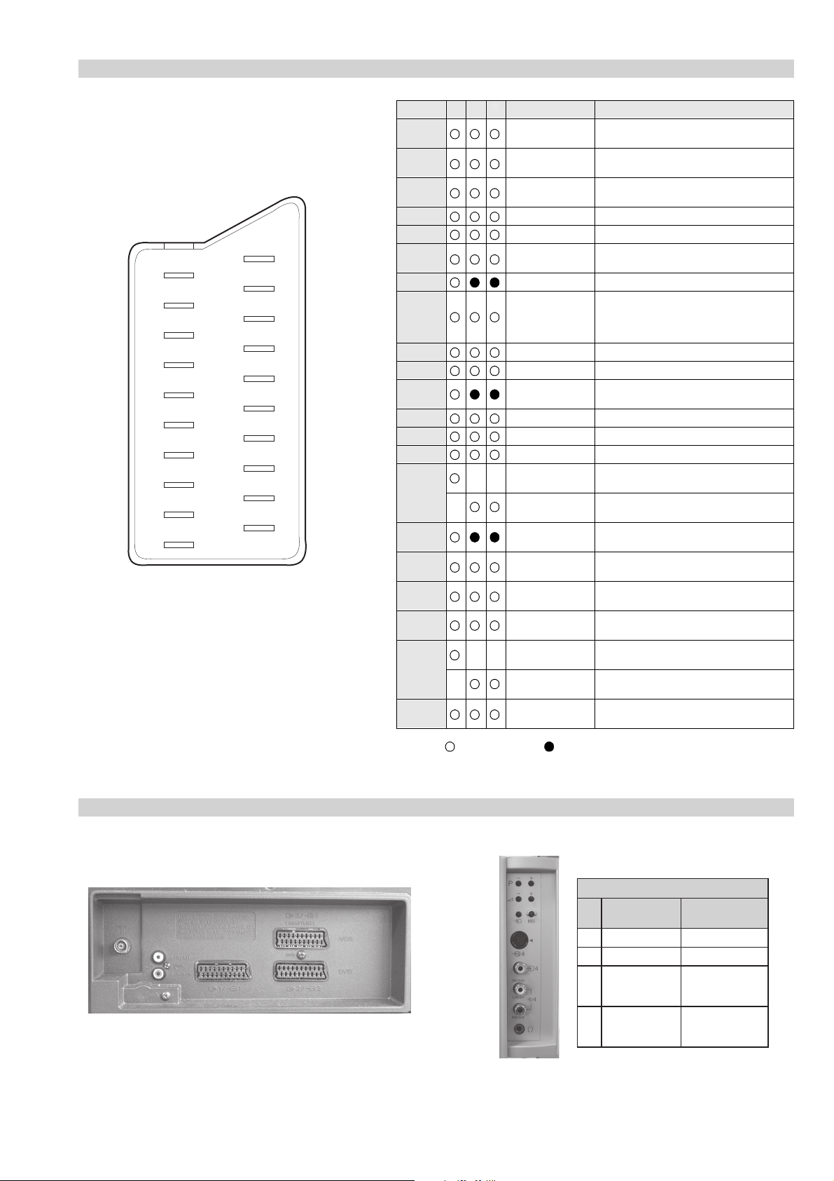
21 pin connector
KP-44PX2/44PX2U
RM-938
21
19
17
15
13
11
9
7
5
3
1
20
18
16
14
12
10
8
6
4
2
Pin No 1 2 4 Signal Signal level
1 Audio output B
2
3
4 Ground (audio)
5 Ground (blue)
6 Audio input A
7 Blue input 0.7 +/- 3dB, 75 ohms positive
8 Function select
9 Ground (green)
10 Open
11 Green Green signal : 0.7 +/- 3dB, 75 ohms,
12 Open
13 Ground (red)
14 Ground (blanking)
15
16 Blanking input
17 Ground (video
18 Ground (video
19 Video output 1V +/- 3dB, 75ohms, positive sync 0.3V
20
21 Common ground
3
(right)
Audio input B
(right)
Audio output A
(left)
(left)
(AV control)
_ _ Red input 0.7 +/- 3dB, 75 ohms, positive
_ (S signal Chroma
input)
(Ys signal)
output)
input)
_ _ Video input 1V +/- 3dB, 75ohms, positive sync 0.3V
_ Video input
Y (S signal)
(plug, shield)
Standard level : 0.5V rms
Output impedence : Less than 1kohm*
Standard level : 0.5V rms
Output impedence : More than 10kohm*
Standard level : 0.5V rms
Output impedence : Less than 1kohm*
Standard level : 0.5V rms
Output impedence : More than 10kohm*
High state (9.5-12V) : Part mode
Low state (0-2V) : TV mode
Input impedence : More than 10K ohms
Input capacitance : Less than 2nF
positive
0.3 +/- 3dB, 75 ohms, positive
High state (1-3V) Low state (0-0.4V)
Input impedence : 75 ohms
(-3+10dB)
(-3+10dB)
1V +/- 3dB, 75ohms, positive sync 0.3V
(-3+10dB)
Connected Not Connected (open) * at 20Hz - 20kHz
Rear Connection Panel Front Connection Panel
niP
oN
S-Video
socket
1dnuorG-
2dnuorG-
3tupni)langisS(Y,mho57Bd3-/+V1
4tupni)langisS(CBd3-/+V3.0
langiS leveLlangiS
noitarugifnocniptekcosoediVS
V3.0.cnySevitisop
Bd01+3-
evitisop,mho57
.cnyS
- 4 -
Page 5
KP-44PX2/44PX2U
RM-938
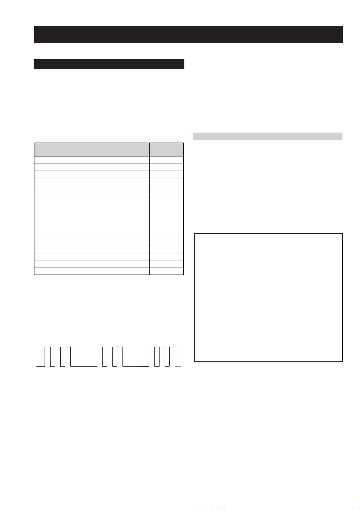
SECTION 1 SELF DIAGNOSIS FUNCTION
1-1. AE-6X Self Diagnostic Software
The identification of errors within the AE-6X chassis is triggered in one of two ways :- 1: Busy or 2: Device failure to respond to IIC. In the
event of one of these situations arising the software will first try to release the bus if busy (Failure to do so will report with a continuous
flashing LED) and then communicate with each device in turn to establish if a device is faulty. If a device is found to be faulty the relevant
device number will be displayed through the LED (Series of flashes which must be counted) See table 1, non fatal errors are reported using this
method.
Each time the software detects an error it is stored within the NVM. See Table 2.
Table 1
egasseMrorrE
rorreoN00
devreseR10
)noitcetorPtnerruCrevO(PCO20
noitcetorPegatloVrevO30
cnySlacitreVoN40
norewoptarorrERKI50
norewoptaegdelwonkcasubCIIonMVN70
noitcetorPlatnoziroH80
norewoptaegdelwonkcaonrenuT90
rorrErossecorPdnuoS01
devreseR11
rorrEetarnacS21
rorrECAD31
rorrEdnekcaB41
rorrEecnegrevnoCcimanyD51
rorrEPIP61
Flash Timing Example : e.g. error number 3
StBy LED
ON ON ON
OFF
OFF
norewoptawolsenilatadro/dnakcolcsubCII60
How to enter into Table 2
DEL
edoC
1. Turn on the main power switch of the TV set.
2. Program Remote Commander for Operation in Service
Mode. [See Page 23].
3. Press ‘VIDEO’ ‘VIDEO’ > ‘MENU’ on the Remote
Commander.
4. Using the Remote Commander, Scroll to the ‘Error Menu’
item using the down arrow key, then press the right arrow
key.
5. The following table will be displayed indicating the error
count.
Table 2
UNEMRORRE
20E
30E
40E
50E
60E
70E
80E
90E
01E
11E
21E
31E
41E
51E
61E
SRUOH
SETUNIM
PCO
PVO
CNYSV
RKI
CII
MVN
TORPH
RENUT
PDNUOS
ETARNACS
CAD
DNEKCAB
-
PIP
EMITGNIKROW
)552,0(
)552,0(
)552,0(
)552,0(
)552,0(
)552,0(
)552,0(
)552,0(
)552,0(
)552,0(
)552,0(
)552,0(
)552,0(
)552,0(
)552,0(
0
0
0
0
0
0
0
0
0
0
0
0
0
0
0
41
7
Note: To clear the error count data press ‘80’ on the Remote
commander.
- 5 -
Page 6
Language
English
Norge
Français
Italiano
Nederlans
Select Language: Confirm: OK
Language
English
Norge
Français
Italiano
Nederlans
Select Language: Confirm: OK
Language
English
Norge
Français
Italiano
Nederlans
Select Language: Confirm: OK
Country
Sverige
Norge-Italia
Schweiz/Suisse/Svizzera
Select Language: Confirm: OK
SECTION 2 GENERAL
Programme Sorting
Programme:
01 TVE2
02 TVE
03 ANT3
Select Channel Confirm:
04 TELE5
05 C+
06 C44
Programme Sorting
Programme:
01 TVE2 41 TVE
02 TVE
03 ANT3
Select new position Move: OK
04 TELE5
05 C+
06 C44
GB
9
MENU
First Time Operation
Broadcast) you wish to rearrange, then press the button.
If you wish to keep the broadcast channels in the tuned order, go to step 7.
automatically appears on the screen enabling you to change the order in which the
After all available channels are captured and stored, the Programme Sorting menu
If you wish to store the channels in a different order:
channels appear on the screen.
a)
b)
6
The operating instructions mentioned here are partial abstracts
from the Operating Instruction Manual. The page numbers of
the Operating Instruction Manual remain as in the manual.
selected channel (TV Broadcast), then press OK.
1 Press the or button to select the programme number with the channel (TV
2 Press the or button to select the new programme number position for your
3 Repeat steps b)1 and b)2 if you wish to change the order of the other channels.
Press the MENU button to remove the menu from the screen.
7
Your projection TV is now ready for use.
No
Yes
automatic tuning?
Do you want to start
OK button to select Yes.
1
B/G
C 01
Auto Tuning
Programme:
Channel:
System
Searching...
Confirm
No channel found
Please connect aerial
continued...
select “-” instead of a country.
recommend to select Russia country in the case that your own country does not
appear in the list.
• If the country in which you want to use the TV se does not appear in the list,
• In order to avoid wrong teletext characters for Cyrillic languages we
The first time you switch on your TV, a sequence of menu screens appear on the TV enabling you to: 1) choose the language
However, if you need to change any of these settings at a later date, you can do that by selecting the appropriate option in
of the menu screen, 2) choose the country in which you wish to operate the TV, 3) search and store all available channels (TV
Broadcast) and 4) change the order in which the channels (TV Broadcast) appear on the screen.
the (Set Up menu) or by pressing the Auto Start Up Button / on the TV set.
Switching On the Projection TV and Automatically Tuning
Connect the Projection TV plug to the mains socket (220-240V AC, 50Hz)
The first time that the TV set is connected, it is usually turned on. If the TV is off, press
The first time you switch on the TV, a Language menu displays automatically on the
the on/off button on the TV set to turn on the TV.
TV screen.
1
Press the or button on the remote control to select the language, then press the
OK button to confirm your selection. From now on all the menus will appear in the
selected language.
2
button to confirm your selection.
The Country menu appears automatically on the TV screen. Press the or button
to select the country in which you will operate the TV set, then press the OK
3
– 6 –
The Auto Tuning menu appears on the screen. Press the
4
any buttons, otherwise automatic tuning will not be completed.
system). In this case, the TV Broadcaster sends a menu in which you can select
In some countries the TV Broadcaster installs the channels automatically (ACI
The projection TV starts to automatically search and store all available broadcast
This procedure could take some minutes. Please be patient and do not press
channels for you.
5
again.
appears automatically on the screen asking you to connect the aerial. Please
connect the aerial (see page 7) and press OK. The auto tuning process will start
your city by pressing the or button and OK to store the channels.
If no channels were found during the auto tuning process then a new menu
First Time Operation
8
Page 7
GB
11
Menu System
Refer to the section "RGB Centring"
on page 17.
0
Enter:
Select:
Detail Set Up
RGB Centring
Personal
Picture Adjustment
Picture Mode
Contrast
Personal
Picture Adjustment
Picture Mode
Contrast
Refer to the section "Picture Adjustment”, on page 12.
AUTO
Brightness
Colour
Sharpness
Reset
Noise Reduction
AUTO
Brightness
Colour
Sharpness
Reset
Noise Reduction
Select: Enter:
Select: Enter Menu:
Natural
Sound Adjustment
Effect
Treble
Bass
Natural
Sound Adjustment
Effect
Treble
Bass
Refer to the section "Sound Adjustment”, on page 12.
Off
On
Stereo
Select: Enter:
Balance
Reset
Dual Sound
Auto Volume
TV Speakers
Off
On
Stereo
Select: Enter Menu:
Balance
Reset
Dual Sound
Auto Volume
TV Speakers
Features
Off
Sleep Timer
Features
On
AUTO
Auto Format
AV3 Output
On
Off
Sleep Timer
Auto Format
Refer to the section "Sleep Timer" on page 13.
AV1
PIP Input
AUTO
AV3 Output
PIP Position
PIP Input
Refer to the section "Auto Format" on page 13.
On
Off
AV1
AUTO
Features
Sleep Timer
Auto Format
AV3 Output
PIP Input
Select: Enter:
AV1
Select: Enter Menu:
PIP Position
Refer to the section "AV3 Output" on page 13.
On
Off
AV1
AUTO
Features
Sleep Timer
Auto Format
AV3 Output
PIP Position
PIP Input
Select: Enter:
On Screen display Menus Guide
PIP Position
Refer to the section "PIP Input" on page 14.
On
Off
AV1
AUTO
Features
Sleep Timer
Auto Format
AV3 Output
PIP Input
Select: Enter:
Refer to the section "PIP Position" on page 14.
On
Off
AV1
AUTO
Features
Sleep Timer
Auto Format
AV3 Output
PIP Input
PIP Position
PIP Position
Select: Enter:
Select: Enter:
Refer to the section "Language/Country" on page 14.
Set Up
Language/Country
Auto Tuning
Programme Sorting
Programme Labels
AV Preset
Manual Programme Preset
Auto Tuning
Programme Sorting
Select NexTView
AV Preset
Manual Set Up
Auto Tuning
Programme Sorting
Select NexTView
AV Preset
Manual Set Up
Set Up
Set Up
Set Up
Language/Country
Auto Tuning
Programme Sorting
Programme Labels
AV Preset
Manual Programme Preset
Refer to the section "Auto Tuning" on page 14.
Refer to the section "Programme Sorting" on page 15.
Reset
Select: Enter Menu:
AUTO
Noise Reduction
Set Up
Select: Enter Menu:
Language/Country
Auto Tuning
Programme Sorting
Programme Labels
AV Preset
Enter:
Select:
Manual Programme Preset
Detail Set Up
Enter:
Select:
Detail Set Up
Enter Menu:
Enter Menu:
Enter Menu:
Select:
Select:
Select:
Detail Set Up
MENU
Start Auto Tuning:
Select:
Set Up
Language/Country
Auto Tuning
Programme Sorting
Programme Labels
AV Preset
Manual Programme Preset
Detail Set Up
AUTO
Personal
Picture Adjustment
Picture Mode
Contrast
Brightness
Colour
Sharpness
Reset
Noise Reduction
Personal
Picture Adjustment
Picture Mode
Contrast
Brightness
Colour
Sharpness
Set Up
Language/Country
Auto Tuning
Programme Sorting
Refer to the section "Programme Labels" on page 15.
Refer to the section "AV Preset" on page 15.
Enter:
Select:
Set Up
Language/Country
Auto Tuning
Programme Sorting
AV Preset
Manual Programme Preset
Detail Set Up
Programme Labels
Programme Labels
Refer to the section "Manual Programme Preset" on page 16.
Enter:
Select:
AV Preset
Manual Programme Preset
Detail Set Up
Enter:
Enter Menu:
Enter Menu:
Enter Menu:
Select:
Set Up
Language/Country
Auto Tuning
Programme Sorting
Programme Labels
AV Preset
Manual Programme Preset
Detail Set Up
Auto Tuning
Auto Tuning
Set Up
Set Up
Set Up
Language/Country
Programme Sorting
Select NexTView
AV Preset
Manual Set Up
Programme Sorting
Select NexTView
AV Preset
Manual Set Up
Auto Tuning
Programme Sorting
Programme Labels
AV Preset
Manual Programme Preset
Detail Set Up
Select:
Select:
Select:
MENU
• the input signal is weak.
• the screen is exposed to spotlights or direct sunlight.
• you watch the teletext broadcast.
The Auto Convergence function does not work when:
The Auto Convergence function works for about 10 seconds. When the white
Press on the mark , on the right side of the projection TV.
Auto converge the Red, Green, and
Blue Lines
Due to the earth’s magnetism, the picture might become undefined and you could see different colours on the outlines of
the images.
In that case, proceed as follows.
Press / button.
1
2
cross disappears from the screen, your projection TV is ready for use.
Adjusting Colour Registration (Convergence)
• you watch NexTView.
• no signal is input.
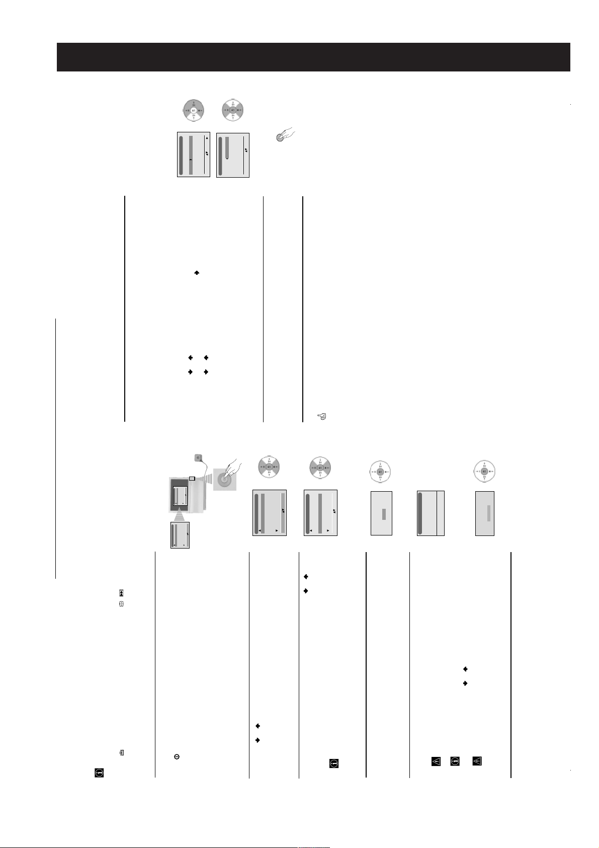
Your projection TV uses an on-screen menu system to guide you through the operations. Use the following buttons on the
Introducing and Using the Menu system
– 7 –
Remote Control to operate the menu system:
Press the MENU button to switch the first level menu on.
1
• To highlight the desired menu or option, press or .
2
• To enter the selected menu or option, press .
• To return to the last menu or option, press .
• To alter the settings of your selected option, press //or.
• To confirm and store your selection, press OK.
Press the MENU button to remove the menu from the screen.
3
First Time Operation - Menu System
10
Page 8
AUTO FORMAT
The “Auto Format” option in the “Features” menu allows you to
To do this: after selecting the option, press . Then press or to
automatically change the aspect ratio of the screen.
select On (if you wish the TV set to automatically switch the screen
format according to the broadcast signal) or Off (if you wish to keep
SLEEP TIMER
The “Sleep Timer” option in the “Features” menu allows you to
select a time period for the TV to switch itself automatically into the
standby mode.
To do this: after selecting the option press , then press or to
set the time period delay (max. of 4 hours).
On
Off
AV1
AUTO
your preference). Finally press OK to store.
On
Off
Features
Sleep Timer
Auto Format
On
Off
AUTO
Personal
Features
Select: Enter:
Sleep Timer
Auto Format
AV3 Output
PIP Input
PIP Position
On
Off
AV1
AUTO
AUTO
Personal
AUTO
AV3 Output
AUTO
GB
S
S
Smart
4:3
14:9
Zoom
Wide
necessary.
If your VCR supports Smartlink, this procedure is not
4 and 4.
To do this: after selecting the option, press . Then press or to
select the desired output signal: TV, AV1, AV2, AV4, YC4 or
AUTO
AV3 Output
AUTO
AUTO.
S
AV1
PIP Input
PIP Position
Select: Enter:
AV1
so that you can record from this Scart any signal coming from the
projection TV or from an external equipment connected to the Scart
AV3 OUTPUT
AV1
PIP Input
PIP Position
Select: Enter:
AV1
connectors 1/ 1 or 2/ 2 or side connectors 4 or
The “AV3 Output” option in the “Features” menu allows you to
select the source to be output from the Scart connector 3/ 3
On
Off
Features
Sleep Timer
Auto Format
On
Off
AUTO
Personal
13
continued...
Menu System
Select: Enter Menu:
Picture Adjustment
Picture Mode
Contrast
Brightness
Colour
Sharpness
Reset
Noise Reduction
Level 1 Level 2 Level 3 / Function
PICTURE ADJUSTMENT
• While watching the TV, you can press the button on the remote control to display the time remaining.
• One minute before the projection TV switches itself into standby mode, the time remaining is displayed on the TV screen automatically.
Picture Adjustment
Picture Mode
Contrast
Brightness
Colour
Features
Select: Enter Menu:
Sleep Timer
Auto Format
AV3 Output
PIP Input
PIP Position
The “Picture Adjustment” menu allows you to alter the picture
adjustments.
To do this: after selecting the item you want to alter press , then
press repeatedly / / or to adjust it and finally press OK
to store the new adjustment.
AUTO
Personal
Sharpness
Reset
Noise Reduction
Select: Enter Menu:
Features
Select: Enter Menu:
Sleep Timer
Auto Format
AV3 Output
PIP Input
PIP Position
Even if you have selected “On” or “Off” in the “Auto Format” option, you can always modify the
format of the screen by pressing repeatedly on the remote control to select one of the following
SOUND ADJUSTMENT
The “Sound Adjustment” menu allows you to alter the sound
adjustments.
To do this: after selecting the item you want to alter, press . Then
press repeatedly / / or to adjust it and finally press OK
Smart: Imitation of wide screen effect for 4:3 broadcast.
4:3: Conventional 4:3 picture size, full picture information.
14:9: Compromise between 4:3 and 16:9 picture size.
Zoom: Widescreen format for letterbox movies.
Wide: For 16:9 broadcast. Full picture information.
formats:
In “Smart”, “Zoom” and “14:9” modes, parts of the top and bottom of the screen are cut off.
Press or to adjust the position of the image on the screen (e.g. to read subtitles).
to store the new adjustment.
Off
On
Stereo
Natural
Picture Adjustment
Picture Mode
Contrast
Brightness
Colour
Sharpness
Reset
Noise Reduction
Select: Enter Menu:
Features
Sleep Timer
Auto Format
AV3 Output
Select: Enter Menu:
PIP Input
PIP Position
the “AV3 Output” to “AUTO” or “TV” for correct unscrambling.
If you select “AUTO”, the output signal will always be the same one that is displayed on the screen.
If you have connected a decoder to the Scart 3/ 3 or to a VCR connected to this Scart, please remember to change back
continued...
Select: Enter:
Picture Adjustment
Picture Mode
Contrast
Brightness
Colour
Sharpness
Reset
Noise Reduction
AUTO
Personal
Select: Enter Menu:
Picture Adjustment
Picture Mode
Contrast
Brightness
Colour
Sharpness
Reset
Noise Reduction
Level 1 Level 2 Level 3 / Function
Menu Guide
Select: Enter:
Sound Adjustment
Effect
Treble
Bass
Balance
Reset
Dual Sound
Auto Volume
TV Speakers
intelligibility and musical realism.
Personal (for individual settings).
Movie (for films).
Off
On
Select: Enter Menu:
Natural
Sound Adjustment
Effect
Treble
Stereo
Select: Enter Menu:
Bass
Balance
Reset
Dual Sound
Auto Volume
TV Speakers
Effect Natural: Enhances clarity, detail and presence of sound by using “BBE High Definition Sound system”*.
Dolby**V: Dolby Virtual, simulates the sound effect of “Dolby Surround Pro Logic”.
Off: Flat response.
Dynamic: “BBE High Definition Sound system”* intensifies clarity and presence of sound for better
Treble Less More
Bass Less More
AUTO
Personal
Picture Adjustment
Picture Mode
Contrast
Brightness
Colour
Sharpness
Reset
Noise Reduction
Picture Mode Live (for live broadcast programmes, DVD and Digital Set Top Box receivers).
• This menu also allows you to customise the picture mode based on the programme you are watching:
• Brightness, Colour and Sharpness can only be altered if “Personal” mode is selected.
select “Off” instead of “AUTO”.
• The Noise Reduction option is set to AUTO to automatically reduce the picture noise visible in the broadcast signal. To cancel this function,
• Hue is only available for NTSC colour signal (e.g: USA video tapes).
• Select Reset and press OK to reset the picture to the factory preset levels.
– 8 –
Mono.
Stereo.
Mono (for mono channel if available).
(e.g. in the case of advertisements).
A (for channel 1).
B (for channel 2).
On: volume level of the channels will stay the same, independent of the broadcast signal
Off:to listen to the TV from an external amplifier connected to the audio outputs on the rear of the projection
• For a bilingual broadcast:
K
TV Speakers On: to listen to the TV from the set speakers.
Balance Left Right
Reset Resets the sound to the factory preset levels.
Dual Sound • For a stereo broadcast:
Auto Volume Off: volume level changes according to the broadcast signal.
TV set.
when the broadcast audio signal is Dolby Surround encoded. The sound effect can also be improved by connecting a suitable external
amplifier (for details refer to “Connecting to external audio Equipment” on page 21).
U.S. Patent No. 4,638,258 and No. 4,482,866. The word “BBE” and BBE Symbol are trademarks of BBE Sound, Inc.
* The “BBE High Definition Sound system” is manufactured by Sony Corporation under license from BBE Sound, Inc. It is covered by
• If you are listening to the TV through headphones, the “Effect” option will automatically be switched to “Off”.
• If you select “Dolby Virtual” on the “Effect” option, the “Auto Volume” option will automatically be switched to “Off” and vice versa.
Laboratories.
**Manufactured under license from Dolby Laboratories. “Dolby”, “Pro Logic” and the double-D symbol are trademarks of Dolby
** This TV has been designed to create the “Dolby Surround” sound effect by simulating the sound of four speakers with two speakers,
Menu System
12
Page 9
to change the order in which the channels (TV Broadcast) appear on
the screen.
To do this: after selecting the option, press and then proceed in
the same way as in step 6 b) of the section “Switching On the
PROGRAMME SORTING
The “Programme Sorting” option in the “Set Up” menu allows you
Projection TV and Automatically Tuning” on page 9.
PROGRAMME LABELS
The “Programme Labels” option in the “Set Up” menu allows you
the programme number with the channel you wish to name.
to name a channel using up to five characters (letters or numbers).
To do this:
1 After selecting the option, press , then press or to select
GB
press or to select a letter or number (select “-“ for a blank),
then press to confirm this character. Select the other four
characters in the same way. Finally press OK to store.
2 Press . With the first element of the Label column highlighted,
AV PRESET
The “AV Preset” option in the “Set Up” menu allows you to
designate a name to the external equipment you have connected to
the input sockets of this projection TV.
To do this:
GAME, CAM, DVD, VIDEO or SAT), press or to select
the desired label and finally press OK to store.
Then with the first element highlighted, press or to
b) If you want to set a different label, select Edit and press .
a) If you want to use one of the 6 predefined label (CABLE,
the input source you wish to name (AV1, AV2 and AV3 are for
the rear Scarts and AV4 for side connectors). Then press .
1 After selecting the option, press , then press or to select
2 A label automatically appears in the label column:
Then with the first element highlighted, press or to
select a letter, number or “-“ for a blank, then press to
confirm this character. Select the other four characters in the
same way and finally press OK to store.
b) If you want to set a different label, select Edit and press .
15
continued...
Menu System
select a letter, number or “-“ for a blank, then press to
confirm this character. Select the other four characters in the
same way and finally press OK to store.
AUTO
Personal
Select: Enter Menu:
Picture Adjustment
Picture Mode
Contrast
Brightness
Colour
Sharpness
Reset
Noise Reduction
Level 1 Level 2 Level 3 / Function
Set Up
Set Up
Set Up
Set Up
Language/Country
Auto Tuning
Auto Tuning
Language/Country
Auto Tuning
Programme Sorting
Programme Labels
AV Preset
Manual Programme Preset
Detail Set Up
Programme Sorting
Select NexTView
AV Preset
Manual Set Up
Programme Sorting
Select NexTView
AV Preset
Manual Set Up
Auto Tuning
Programme Sorting
Programme Labels
AV Preset
Manual Programme Preset
Detail Set Up
Enter:
Select:
Enter Menu:
Enter Menu:
Enter Menu:
Select:
Select:
Select:
Personal
Picture Adjustment
Picture Mode
Contrast
Brightness
Colour
Sharpness
Reset
AUTO
Noise Reduction
Select: Enter Menu:
Set Up
Language/Country
Auto Tuning
Auto Tuning
Set Up
Set Up
Set Up
Language/Country
Auto Tuning
Programme Sorting
Programme Labels
AV Preset
Manual Programme Preset
Detail Set Up
Programme Sorting
Select NexTView
AV Preset
Manual Set Up
Programme Sorting
Select NexTView
AV Preset
Manual Set Up
Auto Tuning
Programme Sorting
Programme Labels
AV Preset
Manual Programme Preset
Detail Set Up
Enter:
Select:
Enter Menu:
Enter Menu:
Enter Menu:
Select:
Select:
Select:
Personal
Picture Adjustment
Picture Mode
Contrast
Brightness
Colour
Sharpness
Reset
AUTO
Noise Reduction
Select: Enter Menu:
Set Up
Language/Country
Auto Tuning
Auto Tuning
Set Up
Set Up
Set Up
Language/Country
Auto Tuning
Auto Tuning
Programme Sorting
Programme Labels
AV Preset
Manual Programme Preset
Detail Set Up
Programme Sorting
Select NexTView
AV Preset
Manual Set Up
Programme Sorting
Select NexTView
AV Preset
Manual Set Up
Programme Sorting
Programme Labels
AV Preset
Manual Programme Preset
Detail Set Up
Enter:
Select:
Enter Menu:
Enter Menu:
Enter Menu:
Select:
Select:
Select:
continued...
PIP INPUT
The “PIP Input” option in the “Features” menu allows you to select
To do this: after selecting the option, press . Then press
the source you want to watch in the “PIP” screen.
AUTO
Personal
Select: Enter Menu:
Picture Adjustment
Picture Mode
Contrast
Brightness
Colour
Sharpness
Reset
Noise Reduction
Level 1 Level 2 Level 3 / Function
repeatedly or to select the desired source AV1, AV2, AV3,
AV4 or TV. Finally press OK to store.
On
Off
AV1
AUTO
Features
Sleep Timer
Auto Format
AV3 Output
PIP Input
PIP Position
Select: Enter:
On
Off
AV1
AUTO
Features
Select: Enter Menu:
Sleep Timer
Auto Format
AV3 Output
PIP Input
PIP Position
/ button on the remote control.
To watch the “PIP” screen with the selected source, press the
You can swap the screens by pressing the / button on the
remote control.
PIP POSITION
The “PIP Position” option in the “Features” menu allows you to
change the position of the “PIP” screen within the main screen.
A
BB
B
B
A
A
Personal
Picture Adjustment
Picture Mode
Contrast
Brightness
Colour
Sharpness
Reset
To do this: after selecting the option press , , or to select
AUTO
Select: Enter Menu:
Noise Reduction
the desired position. Finally press OK to store.
Off
Features
Sleep Timer
Off
Features
Sleep Timer
On
AUTO
Auto Format
AV3 Output
On
AUTO
Auto Format
AV3 Output
AV1
PIP Input
AV1
PIP Input
PIP Position
PIP Position
– 9 –
Select: Enter:
Select: Enter Menu:
LANGUAGE/COUNTRY
The “Language/Country” option in the “Set Up” menu allows you
to select the language that the menus are displayed in. It also allows
you to select the country in which you wish to operate the projection
TV set.
To do this: after selecting the option, press and then proceed in
the same way as in steps 2 and 3 of the section “Switching On the
Personal
Picture Adjustment
Picture Mode
Contrast
Brightness
Colour
Sharpness
Reset
AUTO
Noise Reduction
Select: Enter Menu:
Projection TV and Automatically Tuning” on page 8.
Set Up
Language/Country
Auto Tuning
Auto Tuning
Programme Sorting
Auto Tuning
Programme Sorting
Set Up
Set Up
Set Up
Language/Country
Auto Tuning
Programme Sorting
Programme Labels
AV Preset
Manual Programme Preset
Select NexTView
AV Preset
Manual Set Up
Select NexTView
AV Preset
Manual Set Up
Programme Sorting
Programme Labels
AV Preset
Manual Programme Preset
Detail Set Up
Detail Set Up
Enter:
Select:
Enter Menu:
Enter Menu:
Enter Menu:
Select:
Select:
Select:
AUTO TUNING
The “Auto Tuning” option in the “Set Up” menu allows you to
automatically search for and store all available TV channels.
To do this: after selecting the option, press and then proceed in
the same way as in the steps 4 and 5 of the section “Switching On the
Projection TV and Automatically Tuning” on page 8.
Set Up
Language/Country
Auto Tuning
Programme Sorting
Programme Labels
AUTO
Personal
Select: Enter Menu:
Picture Adjustment
Picture Mode
Contrast
Brightness
Colour
Sharpness
Reset
Noise Reduction
Auto Tuning
Auto Tuning
Set Up
Set Up
Set Up
Language/Country
Programme Sorting
Select NexTView
Programme Sorting
Select NexTView
Auto Tuning
Programme Sorting
AV Preset
Manual Programme Preset
Detail Set Up
AV Preset
Manual Set Up
AV Preset
Manual Set Up
Programme Labels
AV Preset
Manual Programme Preset
Detail Set Up
Start Auto Tuning:
Select:
Enter Menu:
Enter Menu:
Enter Menu:
Select:
Select:
Select:
Menu System
14
Page 10
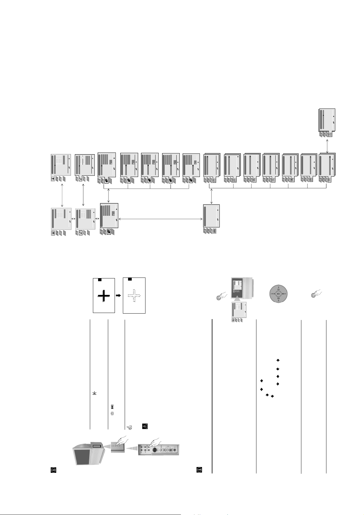
RGB CENTRING
When connecting an RGB source, such as a “PlayStation”, you may
need to readjust the horizontal position of the picture. If this is the
case, you can adjust it through the “RGB Centring” option in the
“Detail Set Up”.
To do this: while watching an RGB source select the “RGB Centring”
option and press . Then press or to adjust the centre of the
picture between –10 and +10. Finally press OK to confirm and store.
0
Enter:
Select:
Detail Set Up
RGB Centring
AUTO
Personal
Picture Adjustment
Picture Mode
Contrast
Brightness
Colour
Sharpness
Reset
Noise Reduction
Select: Enter Menu:
Auto Tuning
Auto Tuning
Set Up
Set Up
Set Up
Language/Country
Programme Sorting
Select NexTView
AV Preset
Manual Set Up
Programme Sorting
Select NexTView
AV Preset
Manual Set Up
Auto Tuning
Programme Sorting
Programme Labels
AV Preset
Manual Programme Preset
Detail Set Up
Enter Menu:
Enter Menu:
Enter Menu:
Select:
Select:
Select:
Level 1 Level 2 Level 3 / Function
GB
17
Menu System
MANUAL PROGRAMME PRESET
The “Manual Programme Preset” option in the “Set Up” menu
allows you to:
Set Up
Language/Country
Auto Tuning
Programme Sorting
Programme Labels
AUTO
Personal
Select: Enter Menu:
Picture Adjustment
Picture Mode
Contrast
Brightness
Colour
Sharpness
Reset
Noise Reduction
Auto Tuning
Programme Sorting
Select NexTView
Auto Tuning
Programme Sorting
Select NexTView
Set Up
Set Up
Set Up
Language/Country
Auto Tuning
Programme Sorting
Programme Labels
Level 1 Level 2 Level 3 / Function
Enter:
Select:
AV Preset
Manual Programme Preset
Detail Set Up
Enter Menu:
Enter Menu:
Enter Menu:
Press or to select which programme number you want to preset the channel on (for VCR, select programme number
AV Preset
Manual Set Up
AV Preset
Manual Set Up
AV Preset
Manual Programme Preset
Detail Set Up
Select:
Select:
Select:
“0”). Then press .
2 The following option is only available depending on the country you have selected in the “Language/Country” menu.
1 After selecting the ”Manual Programme Preset” option, press then with Programme option highlighted press .
Preset channels or the VCR channel one by one to the programme order of your choice. To do this:
a)
TV Broadcast or the channel of the VCR signal. If you do not know the channel number, press or to search for it. When
you tune the desired channel, press OK twice to store.
After selecting the System option, press . Then press or to select the TV Broadcast system (B/G for western
European countries, D/K for eastern European countries, L for France or I for United Kingdom). Then press .
3 After selecting the Channel option, press . Then press the number buttons to enter directly the channel number of the
Label a channel using up to five characters.
To do this: highlighting the Programme option, press the PROG +/- button to select the programme number with the channel
Repeat all the above steps to tune and store more channels.
b)
Fine tune the broadcast reception. Normally the automatic fine tuning (AFT) will give the best possible picture, however you
press or to select a letter, number or “-“ for a blank. Press to confirm this character. Select the other four characters in
the same way. After selecting all the characters, press OK twice to store.
you wish to name. When the programme you want to name appears on the screen, select the Label option and press . Next
To do this: while watching the channel (TV Broadcast) you wish to fine tune, select the AFT option and press . Next press
can manually fine tune the TV to obtain a better picture reception in case the picture is distorted.
or to adjust the fine tuning between -15 and +15. Finally press OK twice to store.
c)
continued...
S
This option is only available depending on the country you have selected in the “Language/Country” menu.
Skip any unwanted programme numbers when they are selected with the PROG +/- buttons.
d)
To cancel this function afterwards, select “No” instead of “Yes” in the step above.
To do this: highlighting the Programme option, press the PROG +/- button to select the programme number you want to skip.
When the programme you want to skip appears on the screen, select the Skip option and press . Next press or to select
View and record scrambled channels when using a decoder connected to Scart 3/ 3 directly or through a VCR.
Yes. Finally press OK twice to confirm and store.
e)
To cancel this function afterwards, select “Off” instead of “On” in the step above.
To do this: select the Decoder option and press . Next press or to select On. Finally press OK twice to confirm and
store.
Menu System
16
– 10 –
Page 11
GB
19
NexTView
Star Wars
|
Euro Sports
Euronews
|
Euro Sports
07
07
06
05
04
03
02
01
Sun 7 : 07 : 01
Sat
Fri
Thu
Wed
Tue
Mon
Songs from the shows
Weather forecast informati
A1 news magazine
Arts show
00 : 30
01 : 30
05 : 30
06 : 30
TV1
TV2
TV3
TV4
Oclock news
Weather forecast informati
A1 news magazine
Arts show
07 : 30
08 : 30
09 : 30
10 : 30
TV5
TV6
TV7
TV8
Remind*:
If you wish to be reminded when the selected programme is
broadcast, press the green button on the remote control. At the
Record Remind
Songs from the shows
TV1 00:30 - 01:30 Thursday 04
Programme description
Sun 9 : 15 : 0 3
time that the programme should be broadcast a reminder
message is displayed on the TV.
Mike's show
Magazine
|
|
Euro Sports
06
Sat
Fantasy film
Songs from the shows
05
Fri
|
|
04
Thu
03
Wed
9 : 00 9 : 30 10 : 00
Magazine
Weather Forecast
Euronews
02
Tue
TV1
TV2
TV3
01
Mon
Home Shopping Europe
News | Arts show
TV4
TV5
Larry King's live |
Euro magazine |
Home Shopping Europe |
TV6
TV7
TV8
Remind*:
If you wish to be reminded when the selected programme is broadcast, press
the green button on the remote control. At the time that the programme
should be broadcast a reminder message is displayed on the TV.
Record Remind
Songs from the shows
TV1 00:30 - 01:30 Thursday 04
Programme description
In case the NexTView provider sends information of more than 8
shows you the list with all the programmes (maximum 5 programmes)
broadcast channels, you can select 8 of them to create your personal list.
music
movies
channel selection:
that you have selected to be reminded about.
remind list:
*
button on the remote control to watch the “Programme List” interface (see fig. 1).
Whilst you are watching TV, and after more than 50% of NexTView data is available (100% data may not be available
Whilst you are watching TV, and after the indication “NexTView” (coloured white) is displayed on the screen, press the
depending on the area) the indication “NexTView” (coloured black) is displayed on the screen. Press the button on
“Programme List” interface:
NexTView is an on-screen electronic programme guide, providing you with programme information for different
When looking for information you can search by theme (sports, art, etc...) or date.
If wrong characters appear when viewing NexTView, use the menu system to enter the “Language/Country” menu (see page
broadcasters.
(depending on availability of service).
NexTView
*
14) and select the same language as the NexTView is broadcasted.
Displaying NexTView
a)
Select a broadcast channel providing a NexTView service. In this case the indication “NexTView” is displayed as soon as data
To see NexTView service you have two different types of NexTView interface. These depend on the % of available data:
is available.
1
2
25
98
25
98
25
98
25
98
25
98
25
98
25
98
25
98
101
153
153
101
153
101
153
101
153
101
153
101
153
101
153
101
TELETEXT
TELETEXT
TELETEXT
TELETEXT
TELETEXT
TELETEXT
TELETEXT
TELETEXT
Index
Programme
News
Sport
Weather
Index
Programme
News
Sport
Weather
Index
Programme
News
Sport
Weather
Index
Programme
News
Sport
Weather
Index
Programme
News
Sport
Weather
Index
Programme
News
Sport
Weather
Index
Programme
News
Sport
Weather
Index
Programme
News
Sport
Weather
the remote control to watch the “Overview” interface (see fig. 2).
b) “Overview” interface:
the screen. Once you have entered the service, the % of data will not increase.
As soon as you enter the NexTView service the % of NexTView data available will be shown in the bottom left corner of
• moving to right or left press or .
• moving up or downwards, press or .
• confirming a selection, press OK.
To navigate through NexTView:
To switch NexTView off, press the button on the remote control.
3
4
Icons for different themes (see the “Icons’ key” section
below)
“Programme List” interface (fig. 1):
This function only works if you have connected a VCR which supports
SmartLink and Timer Programming feature.
Record*:
Date
Programme list
are watching a TV channel which is not a NexTView provider.
”Record” and “Remind” options will be shown on the screen as soon as a programme has been selected, but they will not be shown if you
”Record” and “Remind” will not be available if the programme that you have selected has already started.
*
This function only works if you have connected a VCR which
If you wish to record the selected programme, press the red button on
the remote control.
“Overview” interface (fig. 2):
Icons for different themes (see the “Icons’ key” section
below)
Date
supports SmartLink and Timer Programming feature.
Overview
Record*:
If you wish to record the selected programme, press the
*
full selection list:
red button on the remote control.
Icons’ key:
All the programme information is listed by time
and broadcast channels order.
entertainment
children
arts
sports
news
If this is the case, input another page number
Input 3 digits for the page number, using the numbered buttons.
• If you make a mistake, retype the correct page number.
• If the counter on the screen continues searching, it is because the page is not available.
Press PROG + ( ) or PROG - ().
Whilst you are viewing teletext, press . Press it again to cancel teletext mode.
Press / . Press it again to cancel the freeze.
Press / . Press it again to conceal the information.
wish to view, press .
After selecting the TV channel which carries the teletext service you
To switch on Teletext :
To select a Teletext page:
automatically decreases notoriously to avoid any damage to the picture tube. Press any button of the remote control to
gives you information on how to use the service. To operate teletext, use the remote control buttons as indicated below.
Teletext is an information service transmitted by most TV stations. The index page of the teletext service (usually page 100)
reset the brightness level.
•Teletext errors may occur if you use a channel (TV Broadcast) with a weak signal.
•After 5 minutes viewing the same teletext page and without any button being pressed, the brightness level of the picture
To access the next or preceding page:
To superimpose teletext on to the TV:
To freeze a teletext page:
A teletext page may consist of several sub pages. In this case the page number that appears on the
To reveal concealed information (e.g: answer to a quiz):
To select a sub page:
Press .
upper left corner will change from white to green and one or more arrows will appear next to the page
number. Repeatedly press the or buttons on the remote control to watch the desired sub page.
To Switch Off Teletext:
Teletext
– 11 –
Fastext service lets you access Teletext pages with one button push.
When you are in Teletext mode and Fastext is broadcast, a colour coded menu appears at the bottom
of the teletext page. Press the appropriate coloured button (red, green, yellow or blue) to access
the page corresponding to your menu choice.
Fastext
Teletext
18
Page 12
GB
21
Hi-Fi
Right
speaker
S
~50°
Your sitting position
Left
Hi-Fi
speaker
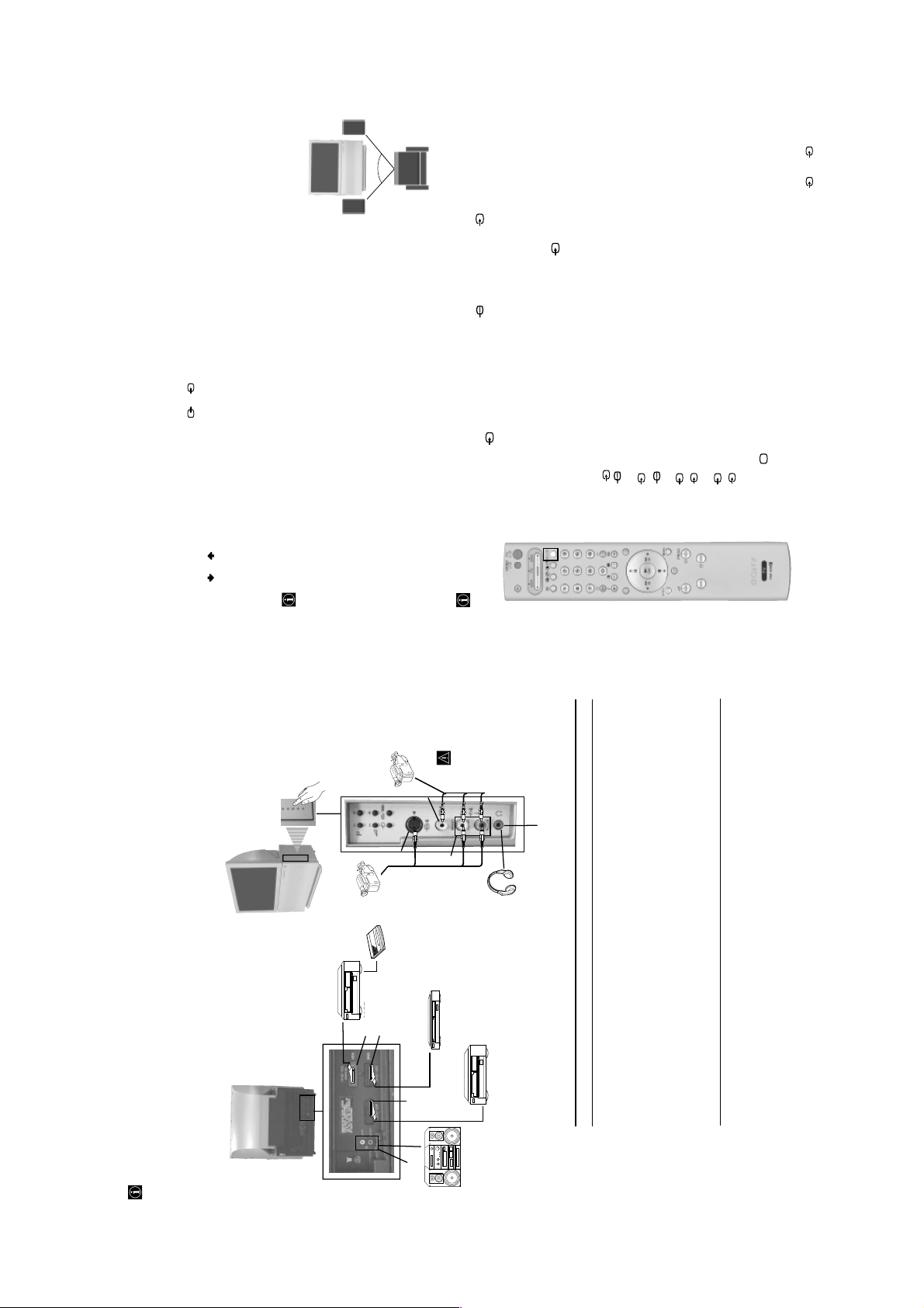
1/ 1. Press the button on the remote control
Y
S
source has been connected.
source has been connected.
Video source has been connected.
G. This symbol appears only if an S Video source has been connected.
2 • RGB input signal through the Scart connector C. This symbol appears only if an RGB
3 • S Video Input signal through the Scart connector D. This symbol appears only if an S
2 • Audio / video input signal through the Scart connector C.
Symbol Input Signals
Connect your equipment to the designated projection TV socket, as it is indicated on the previous
Switch on the connected equipment.
To watch the picture of the connected equipment, press the button repeatedly until the
page.
1
2
3
1 • Audio / video input signal through the Scart connector B
correct input symbol appears on the screen.
3 • Audio/video input signal through the Scart connector D.
4 • S Video Input signal through the front S Video input jack E and Audio signal through
4 • Video input signal through the phono socket F and Audio input signal through G.
S
S
Press button on the remote control to return to the normal TV picture.
For mono equipment
4
Additional Information
Connect the phono plug to the L/G/S/I socket on the side of the TV and select 4 or 4 input
signal using the instructions above. Finally, refer to the “Sound Adjustment” section of this manual
and select “Dual Sound” “A” on the sound menu screen.
bass settings can be modified through the “Sound Adjustment” menu.
Audio level of the external speakers can be modified by pressing the volume buttons on the remote control. Also treble and
Additional Information when connecting equipment
Connecting a VCR
We recommend you connect your VCR to the D socket using a scart lead. If you do not have a scart lead, use the “Manual
Programme Preset” section on page 16 to tune in the channel of the VCR test signal to TV programme number “0”. Also refer to
your VCR instruction manual to get the VCR test signal.
If your video supports SmartLink please refer to the "SmartLink" section of this instruction manual on page 22.
If you have connected a decoder to the Scart 3/ 3 D or through a VCR connected to this Scart:
Select the “Manual Programme Preset” option in the “Set Up” menu and after entering in the “Decoder**” option, select “On” (by
using or ). Repeat this option for each scrambled signal.
**This option is only available depending on the country you have selected in the “Language/Country” menu.
Connecting to external Audio Equipment:
Plug in your Hi-Fi equipment to the audio output sockets A if you wish to amplify the audio output from projection TV. Next ,
using the menu system, select the “Sound Adjustment” menu and set the “TV Speakers” to “Off”.
To enjoy “Dolby Virtual” sound effect through your Hi-Fi equipment:
Place the speakers of your equipment in front of your listening position and beside the
projection TV set but keeping a distance of 50 cm between each speaker and the
projection TV set.
Then by using the menu system, select the menu “Sound Adjustment”. Next select
“Dolby V” on the “Effect” option.
8mm/Hi8/
DVC
camcorder
E
S VHS/Hi8
DVC
camcorder
Decoder
In order to get the input signal of a connected equipment onto the TV screen, you need to select the symbol of the
Using Optional Equipment
picture
distortion:
To avoid
F
G
1 • RGB input signal through the Scart connector B. This symbol appears only if an RGB
connector to which you have connected the device.
e. g. : Your VCR is connected to the connector with the symbol
repeatedly until you see the symbol 1 on the screen.
equipment
connectors
connect
to E and F
at the same
Do not
time.
H
Available output signal
Audio signal.
Video/audio from TV tuner.
Video/audio displayed on TV screen (monitor out).
Video/audio from selected source.
No output.
No output.
No output.
continued...
Audio signal to headphones.
VCR
VCR
C
D
Using the following instructions, you can connect a wide range of optional equipment to your projection TV.
DVD
B
A
Connecting Optional Equipment
– 12 –
Hi-fi
VCR
Acceptable input signal
A No inputs
B Audio/video and RGB signal
C Audio/video and RGB signal
D Audio/video and S video signal
E S Video signal
F Video signal
G Audio signal
H No input
Additional Information
20
Page 13
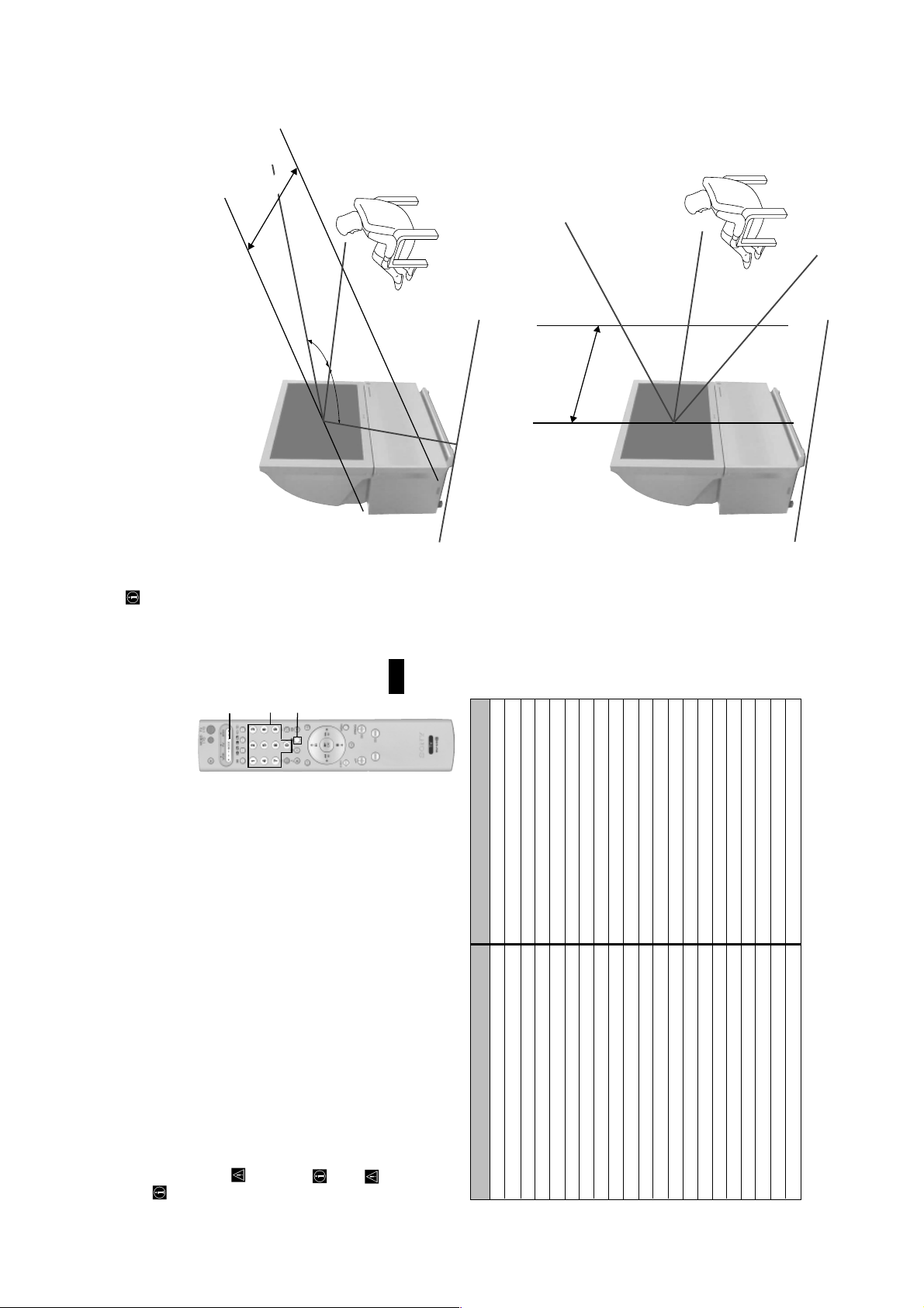
2
1
3
minimum distance 1.7 m
60º
(Optimum viewing position)
(Optimum viewing position)
60º
below.
For the best picture quality, try to position the projection TV so that you can view the screen from within the areas shown
Optimum Viewing Area
Horizontal viewing area
Vertical viewing area
GB
minimum distance 1.7 m
20º
20º
Additional Information
24
23
Additional Information
the correct code set or try the next code listed against the brand.
your brand of DVD or VCR please repeat the above steps. A small label is added inside the
battery door to allow you to record your brand codes.
• If your device is not working or some of the functions do not work please check that you entered
• Your brand codes may be lost if weak batteries are not replaced within a few minutes. To reset
more than one code, enter the first code number.
• Before you start, look up the 3 digit code for your brand of DVD or VCR from the list below. On those brands that have
• Sony will endeavour to update the software according to market changes. Therefore, please refer to code table included
Remote Control Configuration for VCR/DVD
In it’s default condition this remote control will operate the basic functions of this Sony TV, Sony DVDs and most Sony VCRs. To
control VCRs and DVDs of other manufacturers (and some Sony VCR models), please complete the following steps:
If Media Selector is on TV position, code numbers will not be stored.
with the remote control for latest code set.
or DVD) is lit.
Press the Media Selector button on the remote control repeatedly until the required green light (VCR
1
Before the green light goes out, press and hold the yellow button for approximately 6 seconds until the
2
If your selected code is entered correctly, all three green lights will be lit momentarily.
green light starts flashing.
Whilst the green light is flashing, enter all three digits of the code for your brand of VCR or DVD using
the number buttons on the remote control.
3
Turn on your VCR or DVD and check that the main functions work.
4
• Not all brands are covered and not all models of every brand may be covered.
VCR Brand List DVD Brand List
Brand Code Brand Code
SONY (VHS) 301, 302, 303, 308, 309 SONY 001
SONY (BETA) 303, 307, 310 AIWA 021
SONY (DV) 304, 305, 306 DENON 018, 027, 020, 002
AIWA 325, 331, 351 GRUNDIG 009, 028, 023, 024, 016, 003
AKAI 326, 329, 330 HITACHI 025, 026, 015, 004
DAEWOO 342, 343 JVC 006, 017
GRUNDIG 358, 355, 360, 361, 320, 351 KENWOOD 008
HITACHI 327, 333, 334 LG 015, 014
JVC 314, 315, 322, 344, 352, 353, 354, 348, 349 LOEWE 009, 028, 023, 024, 016, 003
LG 332, 338 MATSUI 013, 016
LOEWE 358, 355, 360, 361, 320, 351 ONKYO 022
MATSUI 356, 357 PANASONIC 018, 027, 020, 002
ORION 328 PHILIPS 009, 028, 023, 024, 016, 003
PANASONIC 321, 323 PIONEER 004
PHILIPS 311, 312, 313, 316, 317, 318, 358, 359 SAMSUNG 011, 014
SAMSUNG 339, 340, 341, 345 SANYO 007
SANYO 335, 336 SHARP 019, 027
SHARP 324 THOMSON 012
THOMSON 319, 350 TOSHIBA 003
TOSHIBA 337 YAMAHA 018, 027, 020, 002
– 13 –
Page 14
return to the factory settings.
Solution
• Check the aerial connection.
• Plug the TV in and press the button on the front of the projection TV.
• If the standby indicator is on, press TV button on the remote control.
remote control until the correct input symbol is displayed on the screen.
• Using the menu system, select the “Picture Adjustment” menu and select “Reset” to
• Check that the optional equipment is on and press the button repeatedly on the
• Press the + button on the remote control.
return to factory settings.
desired channel.
Registration (Convergence)” section on page 10.
• Check that “TV Speakers” is “On” in the “Sound Adjustment” menu.
• Check that headphones are not connected.
• Using the menu system, select the “Picture Adjustment” menu and select “Reset” to
• This is not a malfunction. Press the number buttons on the remote control to select the
Tuning (AFT) to obtain better picture reception.
• Adjust the colour registration. For more details, please refer to “Adjusting Colour
• Using the menu system, select the “Manual Programme Preset” menu and adjust Fine
Adjustment” menu and select “Auto” to reduce the noise in the picture.
option and set “AV3 Output” to “TV”.
• Using the menu system, select the “Noise Reduction” option in the “Picture
• Using the menu system, select the “Features” menu. Then enter to “Detail Set Up”
TV.
• Check that the Decoder is not connected on the scart 2/ 2.
• Turn off any equipment connected to the Scart connector on the rear of the projection
country in which you operate the projection TV set. For Cyrillic languages, we
recommend to select Russia country in the case that your own country does not
appear in the list.
the same language that NexTView is broadcast in.
any button being pressed, the projection TV automatically decreases the brightness
level to avoid any damage to the picture tube. To reset the brightness level, press any
button of the remote control.
(VCR, TV or DVD).
has been set correctly. Enter the necessary code set as explained in the “Remote
• Using the menu system, enter to the “Language/Country” menu and select the
• Use the menu system to enter the “Language/Country” menu (see page 14) and select
• This is not a malfunction. After 5 minutes viewing the same teletext page and without
Control Configuration for VCR/DVD” chapter on page 23.
• Check that the Media Selector on the remote control is set to the device you are using
• If the remote control does not operate the VCR or DVD even when the Media Selector
• Replace the batteries.
• Contact your nearest Sony service centre.
Here are some simple solutions to problems which may affect the picture and sound.
Problem
No picture (screen is dark) and no sound.
Poor or no picture (screen is dark), but good
sound.
No picture or no menu information from
equipment connected to the Scart connector.
Good picture, no sound.
No colour on colour programmes.
When you switch on the TV the last channel
you were watching before switching the TV
off does not appear.
Undefined picture with different colour on
the outlines of the images.
Troubleshooting
Noisy picture when viewing a TV channel.
GB
2 x 30 W (music power)
2 x 15 W (RMS)
Sound Output:
Power Consumption:
225 W
Standby Power Consumption:
< 0.7 W
Dimensions (w x h x d) :
approx. 1100 x 1160 x 536 mm.
Weight:
approx. 61 Kg.
Accessories supplied:
1 Remote Control (RM-938)
2 Batteries (IEC designated, AA size)
TEXT memory).
Other features:
•Digital Comb Filter (High resolution).
•100 Hz picture, Digital Plus.
•Teletext, Fastext, TOPtext (250 page
•NICAM.
•Sleep Timer.
•SmartLink (direct link between your
S
3/ 3.
No unscrambling or unstable picture whilst
viewing a scrambled channel with a decoder
connected through the Scart connector
Distorted picture when changing
programmes or selecting teletext.
Wrong characters appear when viewing
teletext.
Wrong characters appear when viewing
NexTView.
projection TV set and a compatible VCR.
For more information on SmartLink,
please refer to the Instruction Manual of
your VCR).
•TV system autodetection.
•Dolby Virtual.
•BBE.
•PIP.
•Auto Format.
•ACI (Auto Channel Installation).
Brightness level of the picture is notoriously
decreased when viewing a teletext page.
Remote control does not function.
The standby indicator on the projection
TV flashes.
If you continue to experience problems, have your projection TV serviced by qualified personnel.
Never open the casing yourself.
Additional Information
26
25
Additional Information
TV system:
Depending on your country selection:
B/G/H, D/K, L, I
Colour system:
PAL
Specifications
SECAM, NTSC 3.58, 4.43 (only Video In)
Channel Coverage:
VHF: E2-E12
UHF: E21-E69
CATV: S1-S20
HYPER: S21-S41
D/K: R1-R12, R21-R69
L: F-2F-10, B-Q, F21-F69
including audio/video input, RGB input, TV
audio/video output.
including audio / video input, RGB input,
monitor audio/video output.
1/ 1 21-pin scart connector (CENELEC standard)
I: UHF B21-B69
Projected picture size:
44” (approx. 112 cm. measured diagonally)
2/ 2 21-pin Scart connector (CENELEC standard)
Rear Terminals
including audio / video input, S video input,
interface.
S
4 S Video input – 4 pin DIN
4 video input – phono jack
audio outputs (Left/Right) - phono jacks
(SMARTLINK)
selectable audio / video output and Smartlink
3/ 3 21-pin Scart connector (CENELEC standard)
4 audio input – phono jacks
S
Side Terminals
headphones jack
– 14 –
Design and specifications are subject to change without notice.
Ecological Paper - Totally Chlorine Free
Page 15
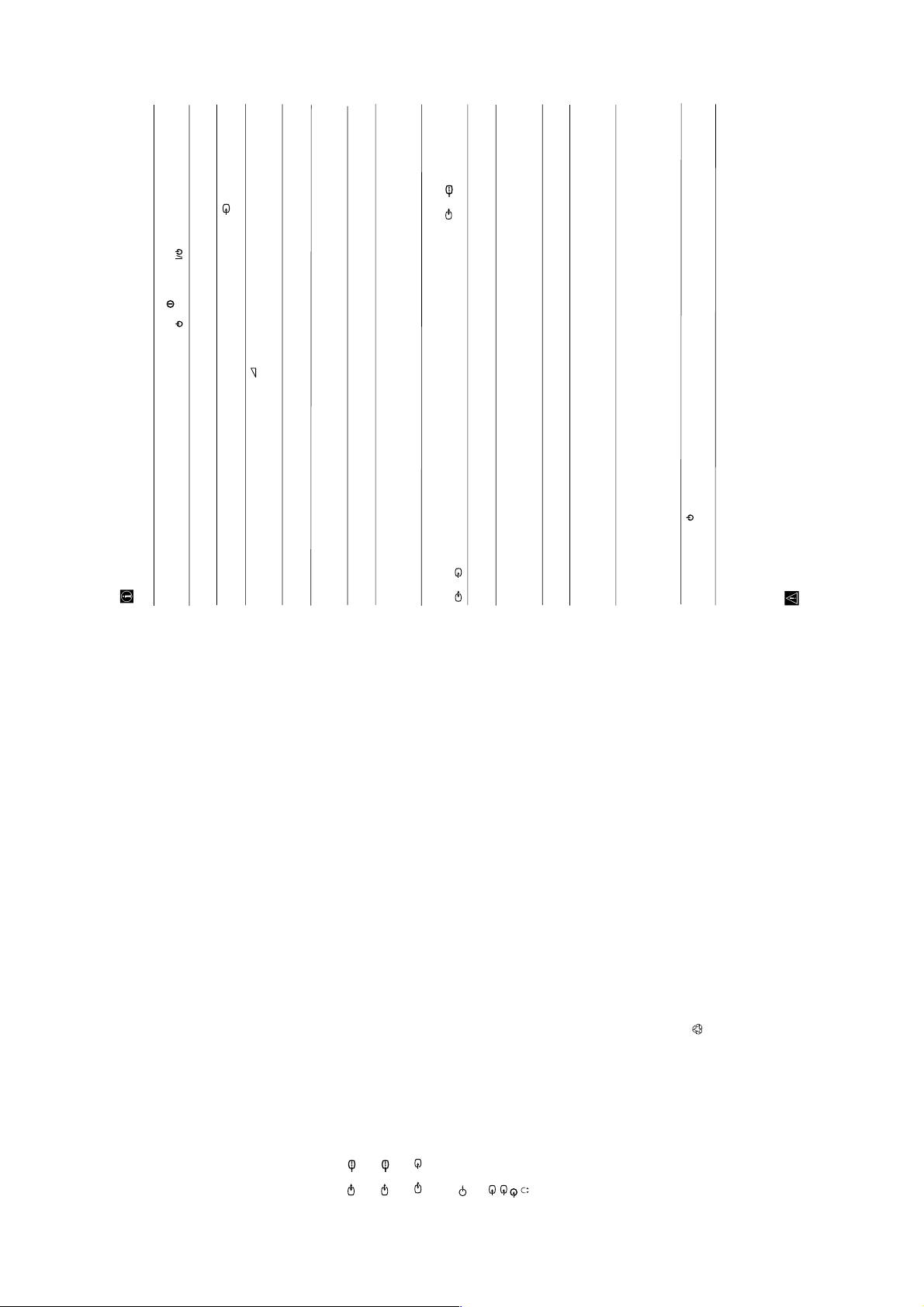
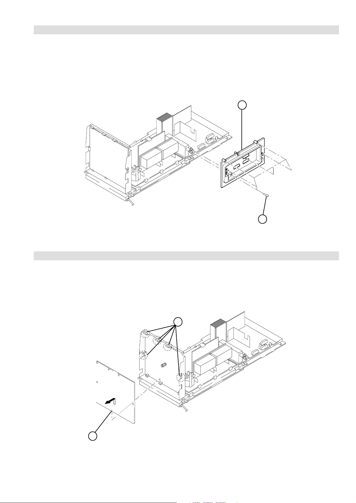
SECTION 3 DISASSEMBLY
KP-44PX2/44PX2U
RM-938
3-1. REAR BOARD REMOVAL
2
Rear board
3-2. MAIN BRACKET BLOCK REMOVAL
Light shield
3
board
2
Two screws
(Hexagon head)
3-3. SERVICE POSITION
1
Twelve screws
(Hexagon head)
Main bracket block
1
3-4. FRONT PANEL REMOVAL
1
Main bracket block
– 15 –
1
Front Panel
2
Two screws
(Hexagon head)
Page 16
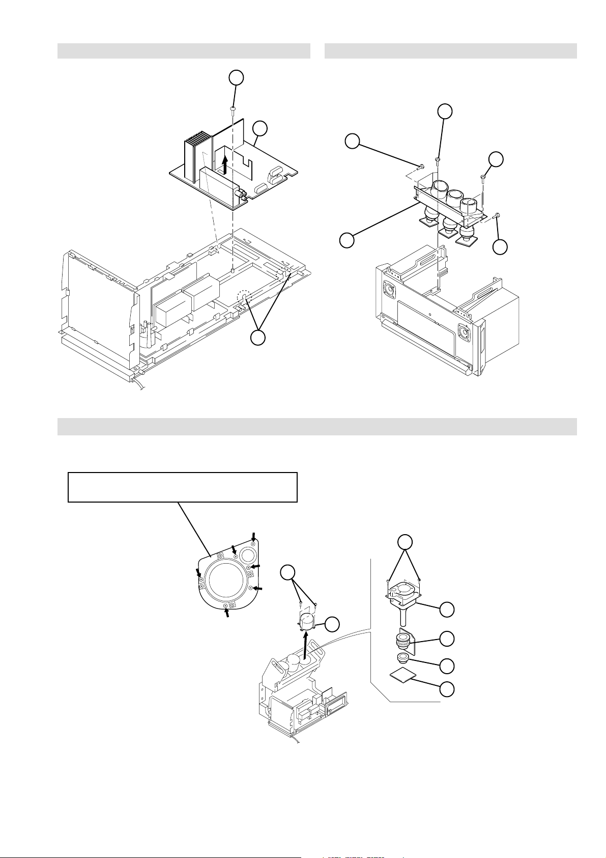
3-5. RESISTOR ASSEMBLY (FOCUS PACK) REMOVAL
KP-44PX2/44PX2U
RM-938
3
Front board
4
Four screws
(Hexagon head)
3-6. H1 AND H3 BOARD REMOVAL
Screw
2
(+BVTP 4x16)
1
Resistor assembly
(Focus pack)
3
Front panel
– 16 –
2
H1 board
1 H3 board
Page 17
3-7. BEZNET BLOCK REMOVAL
2
Beznet block
Eleven screws
1
(+BVTP 4x16)
KP-44PX2/44PX2U
RM-938
4
Four screws
(Hexagon head)
3
Five screws
(Hexagon head)
3-8. HIGH-VOLTAGE CABLE REMOVAL AND
INSTALLATION
(1) Removal
Rubber cap
1
HV cable
2
turn 90
(2) Installation
Rubber cap
1
3-9. AP AND D BOARD REMOVAL
Printed circuit
1
Six screws
(+BVTP 3x12)
2
D board
3
board support
6 AP board
Claw7
Screw
4
(+BVTP 3x12)
4
Gutter
2
HV cable
3
Hook
– 17 –
Screw
4
(+BVTP 3x12)
5
Three claws
Page 18
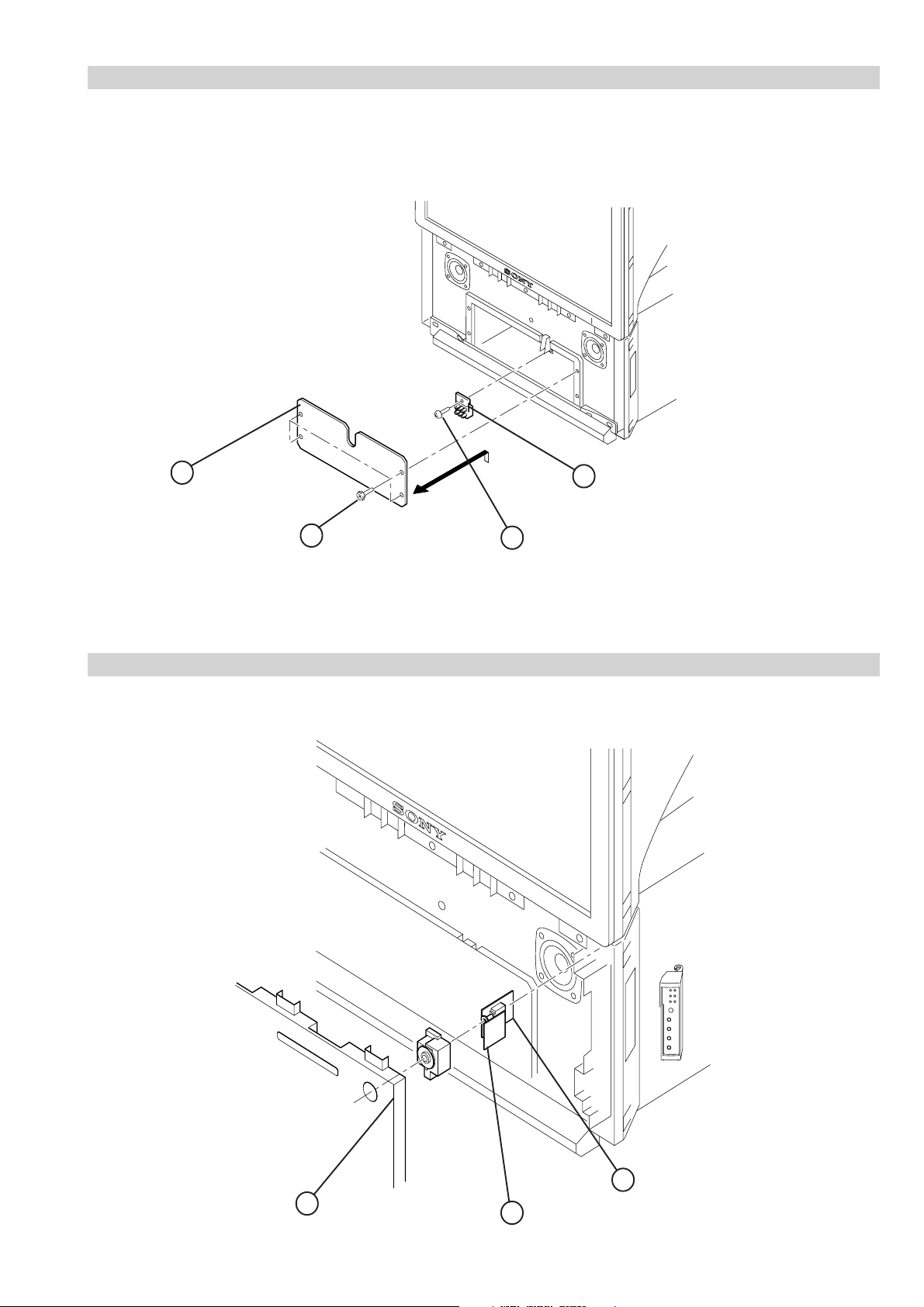
3-10. TERMINAL BOARD REMOVAL
2
Terminal board
KP-44PX2/44PX2U
RM-938
3-11. G BOARD REMOVAL
1
Five claws
Six screws
1
(BVTP 4x16)
2 G board
– 18 –
Page 19
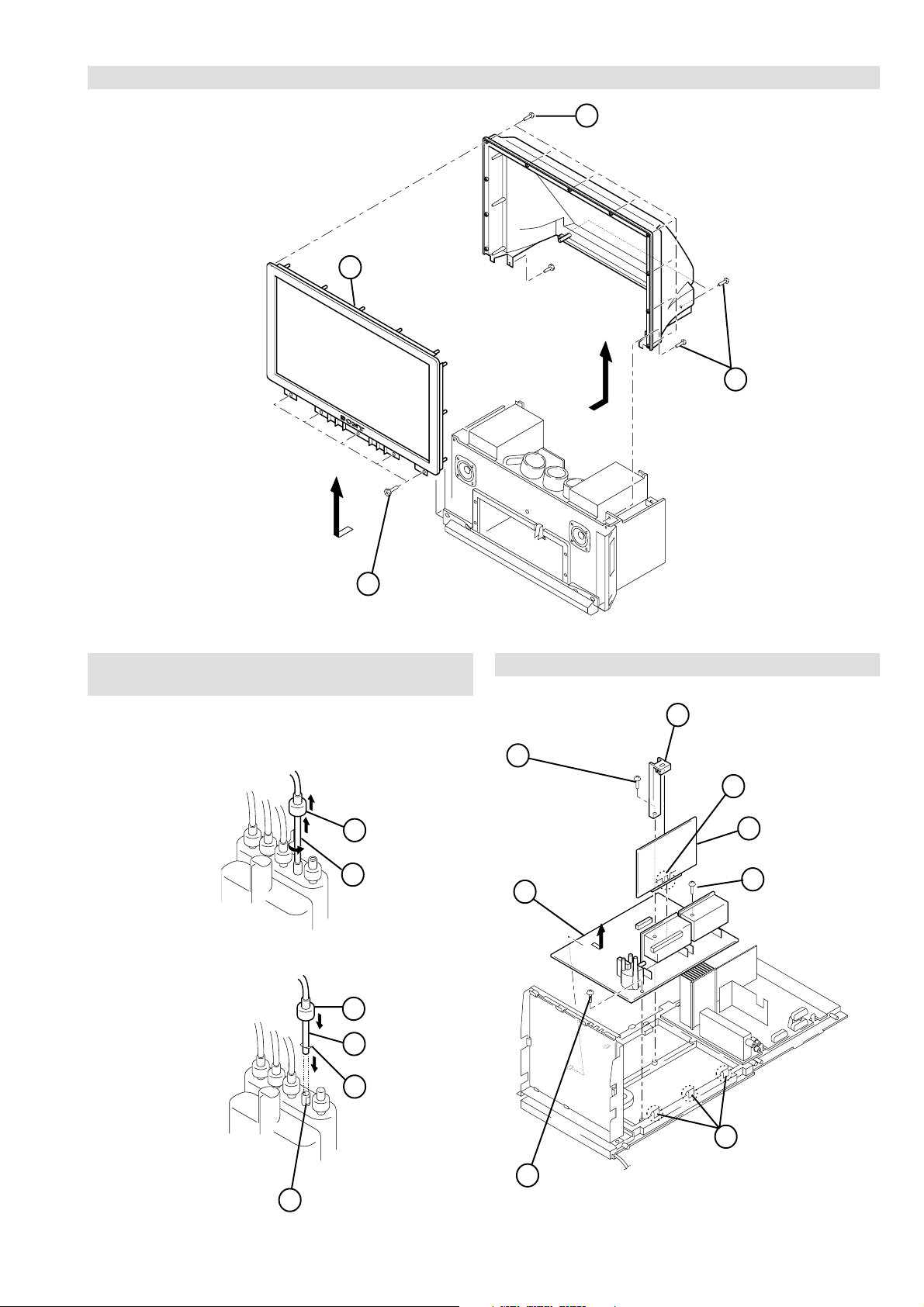
3-12. A BOARD REMOVAL
Screw
1
(+BVTP 3x12)
2
A board
KP-44PX2/44PX2U
3-13. CHASSIS BLOCK REMOVAL
Three screws
2
Screw
(Hexagon head)
3
4
Chassis block
(Hexagon head)
Two screws
1
(Hexagon head)
Screw
3
(Hexagon head)
RM-938
3
3-14. PICTURE TUBE REMOVAL
Removing the arrow-marked screw is strictly inhibited.
If removed, it may cause liquid spill.
Two claws
Four screws
1
(+BTVP 4x16)
Four screws
7
(+BTVP 4x16)
6
Picture tube
2
Lens
5
Deflection yolk
– 19 –
4
Neck assembly
3
CR board
Page 20
SECTION 4 SET-UP ADJUSTMENTS
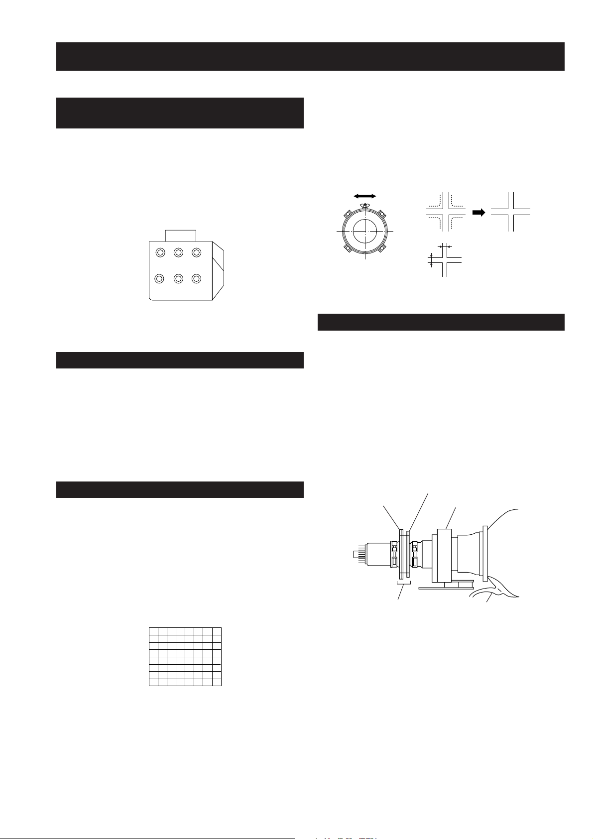
KP-44PX2/44PX2U
RM-938
4-1. SCREEN VOLTAGE ADJUSTMENT
(ROUGH ALIGNMENT)
1. Receive the Monoscope signal.
2. Set 50% BRIGHTNESS and minimum PICTURE.
3. Turn the red VR on the focus pack all the way to the left
and then gradually turn it to the right until the point where
you can see the retrace line.
4. Next gradually turn it to the left to the position where the
retrace line disappears.
RG
RG
B
SCREEN
B
FOCUS
Focus Pack
Fig. 4-1
4-2. SCREEN (G2) ADJUSTMENT
1. Turn on the power of the set.
2. Select VIDEO1 mode without signals.
3. Supply DC 175 ±0.5 V from external power supply to
TP7103 (KR), TP7203 (KG) or TP7303 (KB) of CR board,
CG board and CB board.
4. Adjust red, green and blue screen voltage, with SCREEN
VR on the focus packuntil retraceline disappears .
5. Rotate the green lens and align to obtain the best lens
focus at the center area.
6. Rotate the green focus VR on the focus pack and align to
obtain the best electrical focus in the top right corner.
7. Perform the same alignment for red and blue lenses and
electric focus.
8. Fix lens screw.
A
Minimize both A and B.
Lens
Fig. 4-3
B
Fig. 4-4
4-4. DEFLECTION YOKE TILT ADJUSTMENT
1. Receive the Monoscope signal.
2. Place the caps on the red and blue lens so that only the
green color.
3. Loosen the deflection yoke set screw and align the tilt of
the Deflection yoke so that the bars at the center of
the monoscope pattern are horizontal.
4. After aligning the deflection yoke, fasten it securely to
the funnel-shaped portion (neck) of the CRT.
5. The tilt of the deflection yoke for red and blue is aligned
the same as was done for green.
4-3. FOCUS ROUGH ADJUSTMENT
1. Loose the lens screw.
2. Program Remote Commander for operation in Service
mode (See Page 23).
3. Place the caps on the red and blue lens so that only the
green color is shown.
4. Press “VIDEO” “VIDEO” “5” “6” on the remote
commander to enter 'Projector Engine'. Press “6” twice
on the Commander to display the test signal (crosshatch)
on the screen.
Test signal
Fig. 4-2
4-pole magnet
2-pole magnet
Neck Assy
Make sure deflection yoke is
touching CRT closely.
Fig. 4-5
Deflection yoke
Anode cap
– 20 –
Page 21
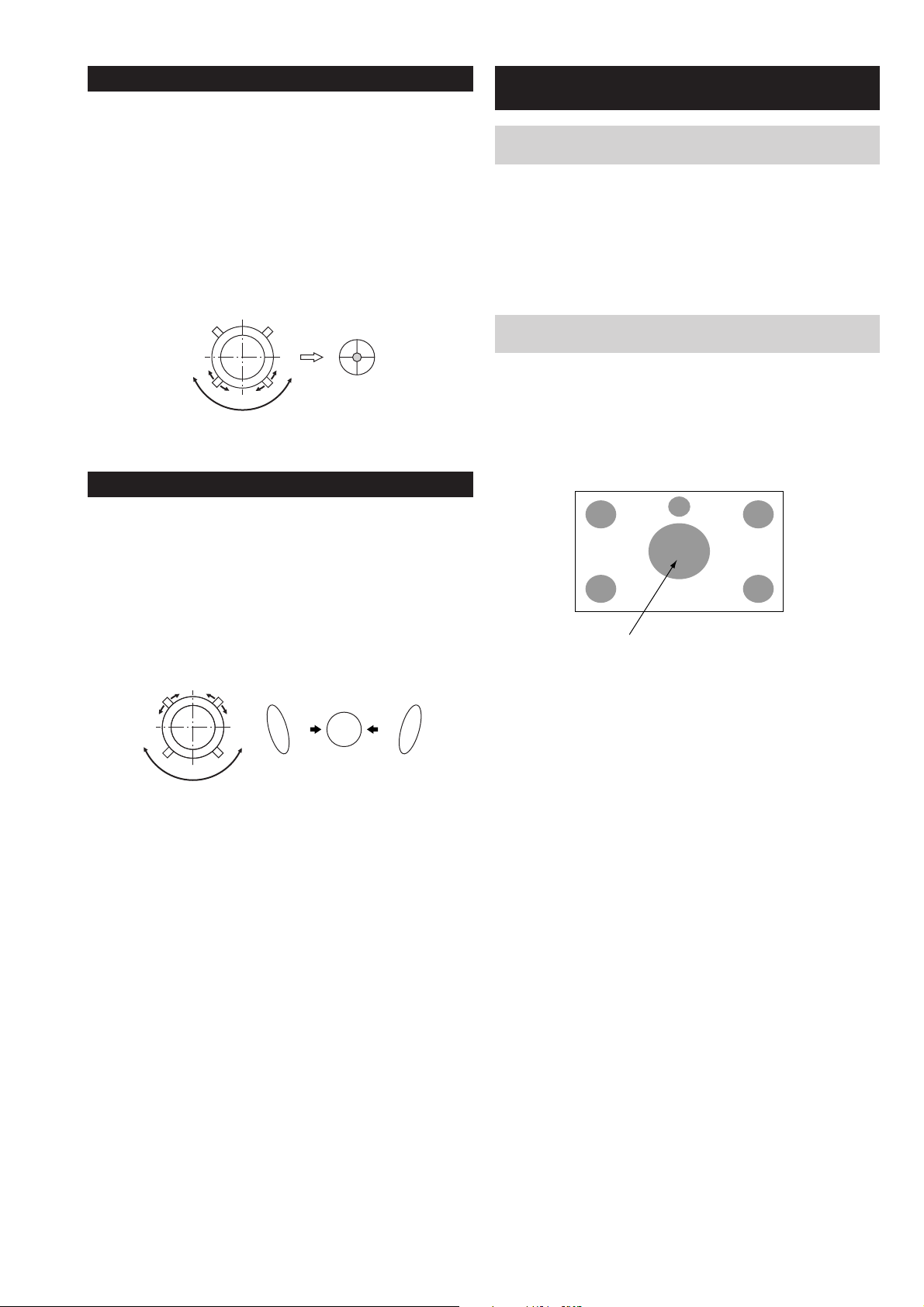
4-5. 2-POLE MAGNET ADJUSTMENT
1. Receive the Dot signal.
2. Place the caps on the red and blue lens so that only the
green color is shown.
3. Turn the green focus VR on the focus pack to the right and
set to over focus to enlarge the spot.
4. Now align the 2-Pole Magnet so that the enlarged spot is in
the center of the just focus spot.
(center of the dot doesn't move)
5. Align the green focus VR and set for just (precise) focus.
6. Perform the same alignment for red and blue.
Use the center dot
Fig. 4-6
4-6. 4-POLE MAGNET ADJUSTMENT
KP-44PX2/44PX2U
RM-938
4-7. GREEN, RED AND BLUE FOCUS
ADJUSTMENT
4-7-1. Green, Red and Blue Lens Focus
Adjustment
1. Receive the Monoscope signal.
2. Place the caps on the red and blue lens so that only the
green color is shown.
3. Rotate the green lens and adjust to obtain the best lens
focus at the center area.
4. Fix lens screw.
5. Repeat above process for red and blue.
4-7-2. Green, Red and Blue Electrical Focus
Adjustment
1. Receive the Monoscope signal.
2. Place the caps on the red and blue lens so that only the
green color is shown.
3. Rotate the green focus VR on the focus pack and adjust
to obtain the best electrical focus at the center area.
4. Repeat above process for red and blue.
1. Receive the Dot signal.
2. Place the caps on the red and blue lens so that only the
green color is shown.
3. Turn the green focus VR on the focus pack to the left and
set to under focus to enlarge the spot.
4. Now align the 4-Pole Magnet so that the enlarged spot
becomes a perfect circle.
5. Perform the same alignment for red and blue.
Use the center dot
Fig. 4-7
OKNG NG
Adjust Point
Fig. 4-8
– 21 –
Page 22
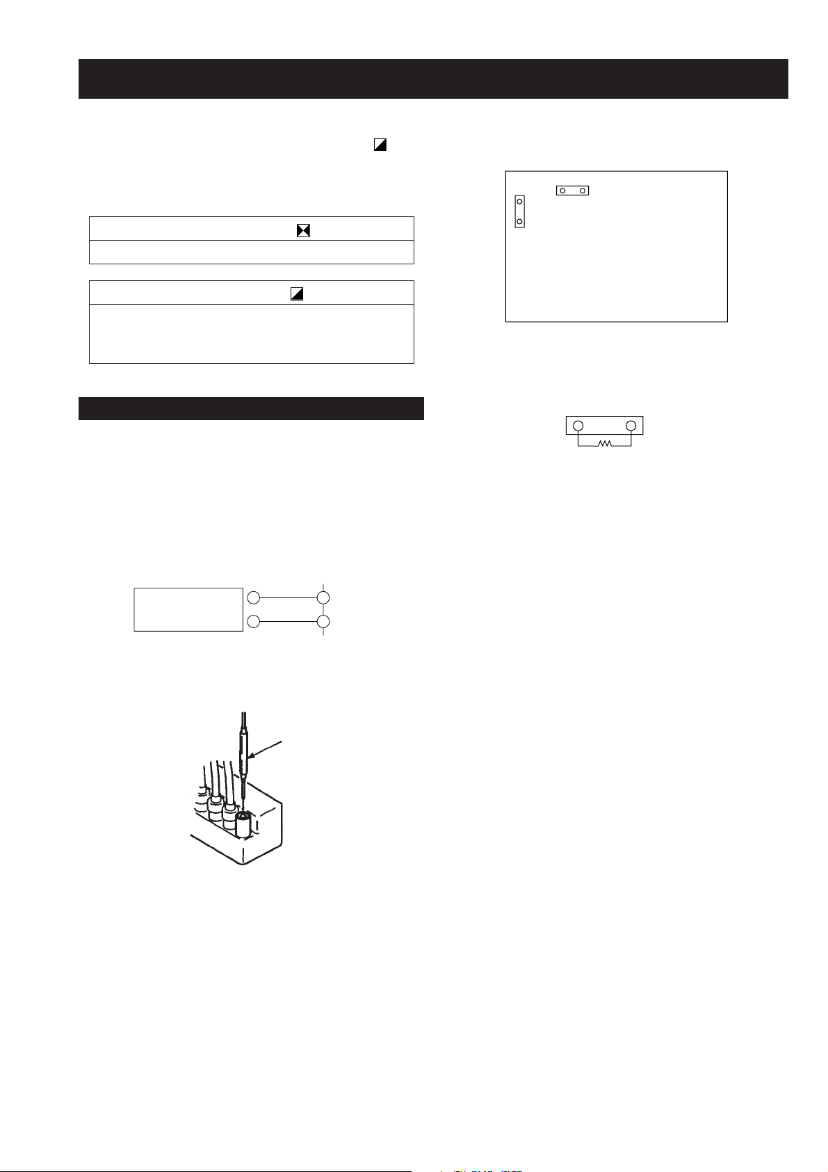
SECTION 5 SAFETY RELATED ADJUSTMENT
When replacing the following components marked with on the
schematic diagram, always check hold-down voltage and if necessary
re-adjust.
D BOARD
CN5003
KP-44PX2/44PX2U
RM-938
– CONDUCTOR SIDE –
Part Replaced ( )
R9901
Part Replaced ( )
D Board C5123, C5127, C5130, C5143, D5115,
D5204, Q5104, R5136, R5138, R5140,
R9901, T5102, T5104, T5103 (FBT)
5-1. HV Hold-Down Adjustment
1. Connect HV static voltmeter to HV Block.
2. Mount a resistor (R9901 : 43 k , 1/4 W, METAL
FILM) at CN5003.
3. Remove CN5002 and connect External Power Supply
to CN5002 1 pin (+135 V) and 2 pin (GND).
4. Turn on the set.
Powe r
Supply
+
–
Fig. 5-1
1
CN5002
2
Remove the cap off
from the unused
terminal and connect a
HV static voltmeter
there.
CN5002
Fig. 5-3
CN5003
R9901
Fig. 5-4
5. Receive the Dot signal and set PICTURE/
BRIGHTNESS to minimum.
6. Slowly up the supply voltage from 0 V to 135 V
until hold-down circuit works (picture disappear).
7. Read the HV static voltmeter of peak HV voltage.
Spec : 33.7 ~ 35.3 kV
8. If Hold-down voltage is less than 33.7 kV then
replace R9901 of 43 k with that of 39 k , and
check if the voltage is within the spec.
9. If hold-down voltage is over than 35.3 kV then
replace R9901 of 43 k with that of 47 k , and
check if the voltage is within the spec.
Fig. 5-2
– 22 –
Page 23
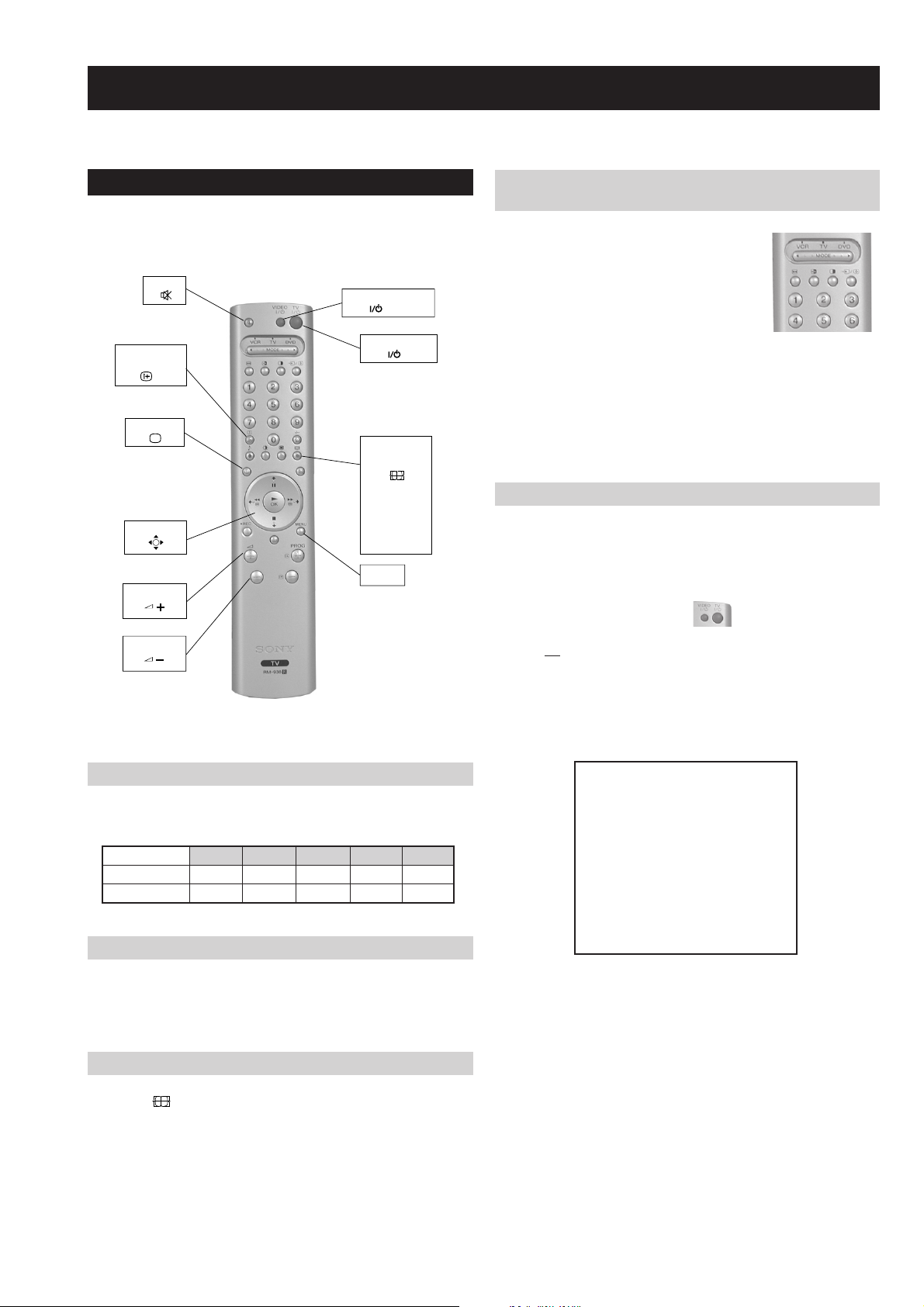
SECTION 6 ELECTRICAL ADJUSTMENTS
KP-44PX2/44PX2U
RM-938
6-1. Adjustments with Commander
Service adjustments to this model can be performed using the
supplied remote Commander RM-938.
MUTE
ON SCREEN
DISPLAY
TV MODE
JOYSTICK
VOLUME +
VOLUME -
VIDEO STANDBY
TV STANDBY
SCREEN
FORMAT
Wide
Zoom
14 : 9
4 : 3
Smart
MENU
6-1-2. Programming the Remote Commander for
Operation in Service Mode
1. Press the VCR/TV/DVD button until the
TV LED lights.
2. Press and hold the yellow button for
approx. 5 seconds until the TV LED
flashes quickly.
3. Press 99999. All three LED’s should light.
The remote commander is now set to Service Mode.
4. To return the remote commander to normal operation mode
repeat steps 1. and 2. then press 00000. All three LED’s
should light.
The remote commander is now set to normal mode.
6-1-3. Setting the TV into Service Mode
1. Program the remote commander for operation in Service
Mode as described above.
2. Turn on the TV main power switch.
3. Press the video standby button on the remote
commander twice.
‘TT ’ will appear in the upper right corner of the screen.
Other status information will also be displayed.
6-1-1. How to Select Each Mode
Adjustment is required in the following modes:
ediW mooZ 9:41 3:4 tramS
LAP
CSTN
OX X XX
OX X XX
1. Selection of Mode Between PAL and NTSC
PAL mode : Enter PAL signal.
NTSC mode : Enter NTSC signal. (VIDEO input only)
2. Selection of Screen Format
1) Press ' (BLUE)' button on the commander.
to select 'Wide', 'Zoom', '14 : 9', '4 : 3' or 'Smart'.
4. Press ‘MENU’ on the remote commander to obtain the
following menu on the screen.
yrtemoeG
amaronaP
ecivreS
etarnacS
PiP
dnuoS
tsujdaFI
uneMrorrE
)'20'raM(90.0vX6EA
hFFhFFatadyrotcaF
G1143PSM:eciveDPSM
5. Move to the corresponding adjustment item using the
up or down arrow buttons on the Remote Commander.
6. Press the right arrow button to enter into the required menu item.
7. Press the ‘Menu’ button on the Remote Commander to quit the
Service Mode when all adjustments have been completed.
Note :
· After carrying out the service adjustments, to prevent the
customer accessing the ‘Service Menu’ switch the TV set
OFF and then ON.
– 23 –
Page 24
6-1-4. Screen Display for Service Menu
KP-44PX2/44PX2U
RM-938
DNUOS
If each item of service menu is selected, the following screen
is displayed.
AMARONAP
MXSOPDR
MYSOPDR
LEDNALB
LOPNALB
NELNALB
MEMARFY
RGABY
MNONAPH
MCSOPCSH
MH1GESH
MOCNIH
ML1GESH
M1CNIH
MH2GESH
M2CNIH
ML2GESH
M3CNIH
MH3GESH
M4CNIH
ML3GESH
M4GESH
MNONAPV
MELBUODV
MCSOPCSV
MH1GESV
MOCNIV
ML1GESV
M1CNIV
MH2GESV
M2CNIV
ML2GESV
M3CNIV
M4CNIV
M3GESV
M4GESV
MSOPROH
MHTDIWROH
GSOPROH
GHTDIWROH
GEMARFROH
POIRP
COIRP
SOIRP
FOIRP
MOIRP
GOIRP
UNEMRORRE
20E
30E
40E
50E
60E
70E
80E
90E
01E
11E
21E
31E
41E
51E
61E
SRUOH
SETUNIM
PCO
PVO
CNYSV
RKI
CII
MVN
TORPH
RENUT
PDNUOS
-
CAD
DNEKCAB
PIP
EMITGNIKROW
)115,0(
)552,0(
)552,0(
)1,0(
)115,0(
)51,0(
)51,0(
)1,0(
)5904,0(
)36,0(
)115,0(
)13,0(
)115,0(
)36,0(
)115,0(
)13,0(
)115,0(
)36,0(
)115,0(
)13,0(
)7402,0(
)1,0(
)1,0(
)38361,0(
)13,0(
)115,0(
)13,0(
)115,0(
)13,0(
)115,0(
)13,0(
)115,0(
)115,0(
)3201,0(
)3201,0(
)7402,0(
)7402,0(
)7402,0(
)7402,0(
)51,0(
)7,0(
)7,0(
)7,0(
)7,0(
)7,0(
)7,0(
ETARNACS
3
01
0
0
0
0
0
1
2302
3
04
0
02
6
0
0
294
9
274
0
483
1
0
9167
0
0
0
0
0
0
0
0
0
0
0
0
069
92
0
3
3
5
6
7
4
1
)552,0(
)552,0(
)552,0(
)552,0(
)552,0(
)552,0(
)552,0(
)552,0(
)552,0(
)552,0(
)552,0(
)552,0(
)552,0(
)552,0(
)552,0(
0
0
0
0
0
0
0
0
0
0
0
0
0
0
0
41
7
N-M
D-M
S-M
M-S
M-D
M-N
EBB
1B
2B
3B
4B
5B
LWS
FWS
DACMACIN
rorrEMACIN
oeretS
sutatS0110000000
ECIVRES
LOCBUS
EUHBUS
PRAHSBUS
THGIRBBUS
TNOCBUS
EVIRD-R
EVIRD-G
EVIRD-B
FFOTUCR
FFOTUCG
FFOTUCB
TXTrB
DSOrB
TSUJDAFI
etumotuA
niaGoiduA
gnitaGL
YRTEMOEG
HTLBA
EDOMLBA
LBAP
EZISV
NOITISOPV
PMOCV
NILV
NOITCERROCS
EZISH
PMANIP
PMOCH
NIPRENROCPU
NIPM
NIPRENROCOL
MUIZEPART
NOITISOPH
WOBCFA
ELGNACFA
KLBTFEL
KLBTHGIR
TCEPSAV
1MITBKA
2MITBKA
RKI
GNH
GNV
)115,0(
)1-,821-(
)721+,0+(
)721+,0+(
)1-,821-(
)3201,0(
)86+,0+(
)69+,69-(
)69+,69-(
)69+,69-(
)69+,69-(
)69+,69-(
)0+,821-(
)04+,5+(
10001
)7402,0(
)721+,821-(
)36,0(
)36,0(
)36,0(
)36,0(
)51,0(
)36,0(
)36,0(
)36,0(
)36,0(
)36,0(
)36,0(
)51,0(
)51,0(
)3,0(
)3,0(
)51,0(
)36,0(
)36,0(
)3,0(
)51,0(
)51,0(
)36,0(
)36,0(
)3,0(
)36,0(
)3,0(
)36,0(
)51,0(
)36,0(
)51,0(
)51,0(
)36,0(
)36,0(
)36,0(
)3,0(
)1,0(
002
02-
02+
01+
01-
694
82+
0+
0+
0+
0+
0+
0+
03+
0
0+
jdA
13
03
31
21
05
jdA
jdA
82
42
64
7
01
1
0
0
0
0
51
53
33
1
7
7
44
23
0
92
2
92
2
04
8
9
43
71
74
2
0
1
0
0
– 24 –
Page 25
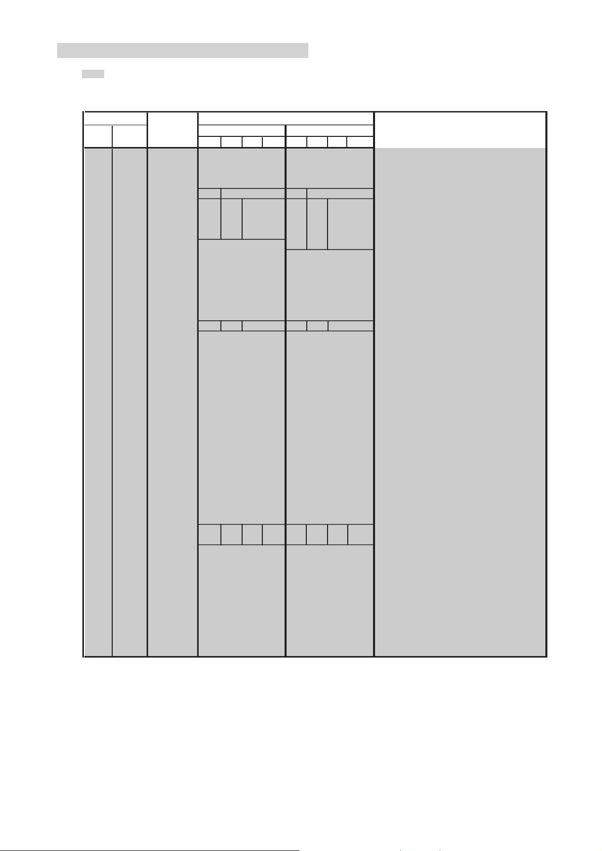
6-1-5. Service List (Projector Engine)
: Fixed data. xxxx : Cannot change.
KP-44PX2/44PX2U
RM-938
Item
No. Name
00 FDIS Switch of display for fine adjustment data
01 COPY Service copy adjustment
02 ALCP Service all copy adjustment
03 OSDH OSD horizontal position of PJED service menu
04 OSDV 32 24 OSD vertical position of PJED service menu
05 FVSL 00 14 00 14 Start position of fine adjustment
06 FVSP 05 17 05 16 Start line of fine adjustment
07 V1DL 01 77 01 52 Value of V1 delay
08 V1CU 750 985 897
09 V1OH Value of V1 offset higher data
10 V1OL Value of V1 offset lower data
11 OEVP Odd/Even select position
12 COHP Horizontal phase for rough adjustment
13 34CS Start center clamp position of H3 and H4 pulse
14 34CW Width center clamp position of H3 and H4 pulse
15 FIHP Horizontal phase for fine adjustment
16 TPHP Horizontal phase for test pattern
17 TPVP 26 58 20 49 Vertical phase for test pattern
18 DFHP Horizontal phase for dynamic focus
19 DFHG Value of horizontal parabola wave for dynamic focus
20 DFVG Value of vertical parabola wave for dynamic focus
21 DFDC Value of center for dynamic focus
22 DFV1 Value of V1 saw wave for dynamic focus
23 SDHP Compensation of horizontal phase for shading
24 SDH1 Value of horizontal saw wave for dynamic focus
25 RVCS Start position of RED vertical clamp
26 RVCW Width of RED vertical clamp
27 GVCS Start position of GREEN vertical clamp
28 GVCW Width of GREEN vertical clamp
29 BVCS Star t position of BLUE vertical clamp
30 BVCW Width of BLUE vertical clamp
31 RHCS Start position of RED horizontal clamp
32 RHCW Width of RED horizontal clamp
33 GHCS Start position of GREEN horizontal clamp
34 GHCW Width of GREEN horizontal clamp
35 BHCS Start position of BLUE horizontal clamp
36 BHCW Width of BLUE horizontal clamp
37 BDVU 23 18 27 21 23 18 27 21 Vertical position for border line 1
38 BDVL 905 686 1061 811 905 686 1061 811 Vertical position for border line 2
39 BDHL Horizontal position for border line 1
40 BDHR Horizontal position for border line 2
41 HBLD Horizontal phase for output of H.Blank out
42 HBLW Width for output of H.Blank out
43 PWM2 PWM2 output width setting of Regi. IC
44 COGV GREEN vertical center offset data for Auto Regi.
45 CORV RED vertical center offset data for Auto Regi.
46 COBV BLUE vertical center offset data for Auto Regi.
47 COGH GREEN horizontal center offset data for Auto Regi.
48 CORH RED horizontal center offset data for Auto Regi.
49 COBH BLUE horizontal center offset data for Auto Regi.
Data Range
Wide Zoom 14 : 9 Smart Wide Zoom 14 : 9 Smart
00, 01
00, 01
00, 01
01 ~ 255
01 ~ 255
00 ~ 15
00 ~ 255
00 ~ 255
00 ~ 4095
00 ~ 255
00 ~ 255
00 ~ 4095
00 ~ 4095
00 ~ 31
00 ~ 31
00 ~ 4095
00 ~ 4095
00 ~ 255
00 ~ 4095
Ð128 ~ 127
Ð128 ~ 127
Ð128 ~ 127
Ð128 ~ 127
00 ~ 4095
Ð128 ~ 127
00 ~ 31
00 ~ 31
00 ~ 31
00 ~ 31
00 ~ 31
00 ~ 31
00 ~ 31
00 ~ 31
00 ~ 31
00 ~ 31
00 ~ 31
00 ~ 31
00 ~ 2047
00 ~ 2047
00 ~ 2047
00 ~ 2047
00 ~ 4095
00 ~ 4095
00 ~ 4095
Ð128 ~ 127
Ð128 ~ 127
Ð128 ~ 127
Ð128 ~ 127
Ð128 ~ 127
Ð128 ~ 127
Standard Data
PAL NTSC
00
00
00
26
15
09
48
1183 Value of V1 count up
30
40
00
1056
4095
14
00
1110
67
100
-90
-40
127
00
00
00
00
00
00
00
00
00
00
00
00
00
00
00
159
1253
00
00
00
00
00
00
00
00
00
03
1056
4095
1110
100
-90
-40
127
00
00
00
00
00
00
00
00
00
00
00
00
00
00
00
159
1253
00
00
00
00
00
00
00
00
00
Name/Description
00
00
00
26
4252
15
17
23
1001880
20
01
14
00
67
3346
– 25 –
Page 26
KP-44PX2/44PX2U
RM-938
Item
No. Name
50 SOGV GREEN vertical skew offset data for Auto Regi.
51 SORV RED vertical skew offset data for Auto Regi.
52 SOBV BLUE vertical skew offset data for Auto Regi.
53 SOGH GREEN horizontal skew offset data for Auto Regi.
54 SORH RED horizontal skew offset data for Auto Regi.
55 SOBH BLUE horizontal skew offset data for Auto Regi.
56 ZOGH GREEN horizontal size offset data for Auto Regi.
57 ZORH RED horizontal size offset data for Auto Regi.
58 ZOBH BLUE horizontal size offset data for Auto Regi.
59 LOGH GREEN horizontal linearity offset data for Auto Regi.
60 LORH RED horizontal linearity offset data for Auto Regi.
61 LOBH BLUE horizontal linearity offset data for Auto Regi.
62 ERR Auto Regi. Error code
63 ADTM A/D data input timing of Auto Regi.
64 VUP Auto Regi. Pattern upper vertical position
65 VUPM Auto Regi. Pattern upper middle vertical position
66 VMID Auto Regi. Pattern middle vertical position
67 VLOM Auto Regi. Pattern lower middle vertical position
68 VLOW Auto Regi. Pattern lower vertical position
69 HLE Auto Regi. Pattern left horizontal position
70 HLEM Auto Regi. Pattern left middle horizontal position
71 HMID Auto Regi. Pattern middle horizontal position
72 HRIM Auto Regi. Pattern right middle horizontal position
73 HRIV Auto Regi. Pattern right horizontal position
74 SFTF Switch of shift fast 00 : Normal 01 : Quick
75 ACTL Account time counter lower byte
76 ACTH Account time counter higher byte
77 SLSW Auto Regi. Adjustment item select
CENT GREEN Horizontal/Vertical center
SKEW GREEN Horizontal/Vertical skew
SIZE GREEN Horizontal/Vertical size
GRN
BLU
RED
KEY GREEN Vertical keystone
PIN GREEN Horizontal/Vertical pincushion
MLIN GREEN Horizontal mid linearity
MSIZ GREEN Horizontal mid size
CENT BLUE Horizontal/Vertical center
SKEW BLUE Horizontal/Vertical skew
SIZE BLUE Horizontal/Vertical size
KEY BLUE Vertical keystone
PIN BLUE Horizontal/Vertical pincushion
MLIN BLUE Horizontal mid linearity
MSIZ BLUE Horizontal mid size
CENT RED Horizontal/Vertical center
SKEW RED Horizontal/Vertical skew
SIZE RED Horizontal/Vertical size
KEY RED Vertical keystone
PIN RED Horizontal/Vertical pincushion
MLIN RED Horizontal mid linearity
MSIZ RED Horizontal mid size
Data Range
Wide Zoom 14 : 9 Smart Wide Zoom 14 : 9 Smart
–128 ~ 127
–128 ~ 127
–128 ~ 127
–128 ~ 127
–128 ~ 127
–128 ~ 127
–128 ~ 127
–128 ~ 127
–128 ~ 127
–128 ~ 127
–128 ~ 127
–128 ~ 127
00 ~ 255
00 ~ 127
00 ~ 2047
00 ~ 2047
00 ~ 2047
00 ~ 2047
00 ~ 2047
00 ~ 4095
00 ~ 4095
00 ~ 4095
00 ~ 4095
00 ~ 4095
00, 01
00 ~ 255
00 ~ 255
00 ~ 03
–512 ~ 511
–512 ~ 511
–512 ~ 511
–512 ~ 511
LIN GREEN Horizontal/Vertical linearity
–512 ~ 511
–512 ~ 511
–512 ~ 511
–512 ~ 511
–512 ~ 511
–512 ~ 511
–512 ~ 511
–512 ~ 511
LIN BLUE Horizontal/Vertical linearity
–512 ~ 511
–512 ~ 511
–512 ~ 511
–512 ~ 511
–512 ~ 511
–512 ~ 511
–512 ~ 511
–512 ~ 511
LIN RED Horizontal/Vertical linearity
–512 ~ 511
–512 ~ 511
–512 ~ 511
–512 ~ 511
PAL NTSC
00
00
00
00
00
00
00
00
00
00
00
00
00
80
31
00
290
00
560
135
00
640
00
1170
00
00
00
00
000/000
000/000
000/–200
000/000
xxxx/000
000/250
000/xxxx
000/xxxx
000/000
000/000
000/–200
000/000
xxxx/000
000/250
000/xxxx
000/xxxx
000/000
000/000
000/–200
000/000
xxxx/000
000/250
000/xxxx
000/xxxx
Standard Data
Name/Description
00
00
00
00
00
00
00
00
00
00
00
00
00
120
45
00
475
00
930
135
00
645
00
1170
00
00
00
00
000/000
000/000
000/–200
000/000
xxxx/000
000/250
000/xxxx
000/xxxx
000/000
000/000
000/–200
000/000
xxxx/000
000/250
000/xxxx
000/xxxx
000/000
000/000
000/–200
000/000
xxxx/000
000/250
000/xxxx
000/xxxx
– 26 –
Page 27
6-2. Registration Adjustments
6-2-1. Setup for Adjustment
KP-44PX2/44PX2U
RM-938
7. Adjust “V-Size” and “H-Size” so that the picture size is
within the specification.
1. Marking
1) At the 4 insides of the screen, locate the middle. Use a tape
measure to identify the middle.
: middle
2. Data Setting
1) Set PAL-Wide mode.
2) Program the remote commander for operation in Service
Mode (See Page 23).
3) Press 'VIDEO', 'VIDEO' ,'5', '6' on the commander to enter
Projector Engine.
4) Press '7' + '0' (READ) buttons on the commander to read the
data from NVM. Then all the default data are restored.
SPEC Overscan Spec. = 7.5%
Input Signal H SIZE V SIZE
PAL SPCB 16.7 ± 0.1 sq. 12.5 ± 0.1 sq.
V-Size
H-Size
8. Adjust the following items so as to attain the optimum
picture.
V-Linear
S-Corr
Note : When replacement of printed circuit boards, devices or
CRTs, and major correction is necessary, press '5' + '0'
(PJE INITIAL) buttons to initialize the data in the
Projector Engine mode.
Press '
(MUTE)' + '0' buttons on the commander to
write the data.
6-2-2. Main Deflection Adjustment
The data values are same in all modes, and therefore the
adjustment for the PAL-Wide mode only is performed here.
1. Place the caps on the red and blue lenses so that only the
green color is displayed.
2. Enter the PAL SPCB signal and set the TV to PAL mode.
3. Set the screen format to “Wide”.
4. Program the remote commander for operation in Service
Mode and enter Service Menu(See Page 23).
5. Select 'Geometry' from the service menu.
6. Adjust “V-Position” and “H-Position” so that the picture is
displayed in the center of screen.
V-Position
Pin Amp
Up-CPin
Lo-CPin
Trapezium
AFC-Bow
AFC-Angle
H-Position
– 27 –
Page 28
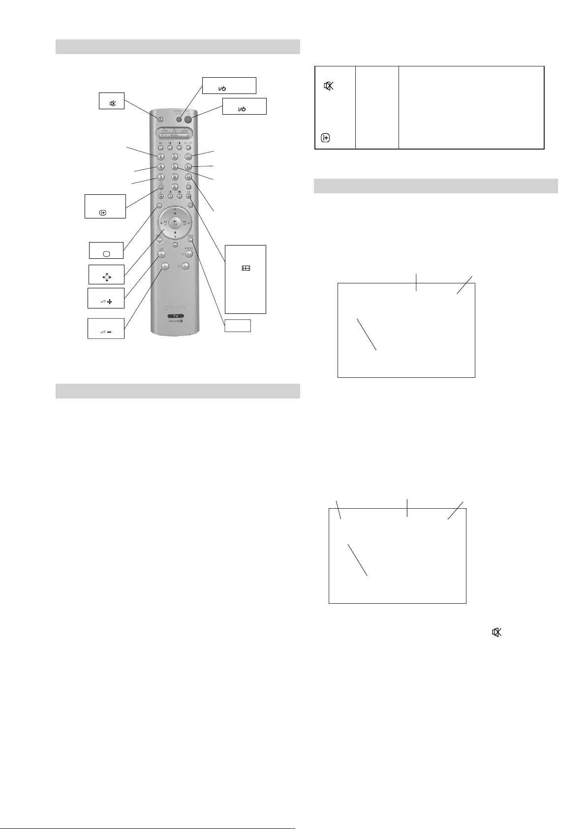
6-2-3. Operation Method for Projector Engine Mode
VIDEO STANDBY
MUTE
Write data to NVM
Adjustment item up
Adjustment item down
Read data from NVM
ON SCREEN
DISPLAY
Copy PAL data to NTSC
TV MODE
JOYSTICK
VOLUME +
VOLUME -
TV STANDBY
Color change
Internal test signal
Initialise data
(Not stored)
Mode select
(Fine or Rough)
SCREEN
FORMAT
Wide
Zoom
14 : 9
4 : 3
Smart
MENU
KP-44PX2/44PX2U
RM-938
Commander Function
Buttons Mode Description
+ - WRITE Writes data to NVM.
7 + - READ Reads data from NVM.
5 + - PJE Service data initialization. Not stored.
+ - PJE Copies data of PAL mode to NTSC mode
2. Operation Method for Rough Adjustment
1) Press 'VIDEO', 'VIDEO' ,'5', '6' on the commander to enter
Projector Engine.
2) Press '1' or '4' button on the commander to select the item, and
press v, V, b, B key on the joystick to change the data.
INITIAL
(Be sure not to use usually)
Item No.
PJE 00 00
FDIS |
Data
1. Functions of Keys on Commander
• 1 : Changes adjustment item. (item No. moves up)
: Marker moves clockwise from center to outside.
(in fine adjustment mode)
• 4 : Changes adjustment item.
(item No. moves down)
: Marker moves counterclockwise from outside
to center. (in fine adjustment mode)
• v V b B: Changes data value. (up or down)
: Marker moves up, down, or to the left or right.
(in fine adjustment mode)
• 3 : Changes adjustment color.
(except item No. 00~77) GRN B BLU B RED
• 6 : Displays or changes internal test signals.
: crosshatch + external signal B crosshatch only
B crosshatch only B dot only B off
• 9 : Switches adjustment mode.
rough adjustment mode c fine adjustment mode
• (OK) : Switches marker moving method.
(in fine adjustment mode)
joystick (v, V, b, B) keys c 1 and 4 buttons
Adjustment
Item
v, B : Data up
V, b : Data down
3) Select “GRN CENT” . When BLU or RED is displayed,
press “3” button on the commander to change the adjustment
color in the order of GRN c BLU c RED.
4) In the GRN, BLU, or RED mode, v, V keys on the joystick
can change the data in vertical direction, or b, B keys in
horizontal direction.
Color
GRN 000 000
CENT
Data (H)
Data (V)
b : Data (H) up
B : Data (H) down
Adjustment
Item
5) Before returning to the Service menu, press “
v : Data (V) up
V : Data (V) down
(MUTE)”
+“0” buttons on the commander to write the data.
(Omission of this operation causes the set data to be returned
to the data before adjustment)
6) Press “MENU” button on the commander to return to the
Service menu.
– 28 –
Page 29
3. Operation Method for Fine Adjustment
Push the joystick
to v
Push the joystick
to V
Push the joystick
to B
Push the joystick
to b
Push the joystick
to v
Push the joystick
to V
Push the joystick
to B
Push the joystick
to b
(in GRN, BLU, or RED Mode)
KP-44PX2/44PX2U
RM-938
6-2-4. Projector Engine Adjustment
(Sub Deflection Adjustment)
1) Select the Projector Engine mode.
2) Select FDIS so that the data at each position can be
displayed in the fine adjustment mode, and set the data to
“01”.
3) Press “9” button on the commander, and the fine adjustment
mode will be active where a green marker appears in the
center of screen (in the case of GRN mode).
4) Press “
(OK)” button, and the marker color will be
switched between green (GRN mode) and white alternately.
5) Use “1” or “4” button on the commander, or the joystick to
move the marker to the position to be adjusted, where
fine adjustment can be made.
• When marker color is white.
(in this case, fine adjustment is disabled)
Operating the joystick can move the marker up, down, or to
the left or right freely.
• When marker color is green. (GRN mode)
Adjustment
aa
a : Yes – : No
aa
Adjustment Type
Adjustment Item GRN RED BLU
H / V H / V H / V
CENT a / aa / aa / a
SKEW a / aa / aa / a
SIZE a / aa / aa / a
LIN a / aa / aa / a
KEY – / a – / a – / a
PIN a / aa / aa / a
MLIN a / – a / – a / –
MSIZ a / – a / – a / –
<Adjustment for PAL-Wide Mode>
1. Green Adjustment
1) Place the caps on the red and blue lenses so that only the
green color is displayed.
2) Enter the PAL SPCB signal to set the PAL mode.
3) Set the screen format to “Wide”.
4) Select the Projector Engine mode.
5) Press “6” button on the commander to display internal test
signal (crosshatch).
6) Select “GRN CENT”, and adjust so that the picture coincide
in the center of screen.
1 : moves the marker clockwise from center to outside.
4 : moves the marker counterclockwise from outside to center.
• Fine adjustment can be made on the basis of marker
position using v, V, b , B keys on the joystick.
Movement when v key
on joystick is pressed.
CROSSHATCH
Movement when B key
on joystick is pressed.
CROSSHATCH
6) Press “9” button on the commander to return to the rough
adjustment mode.
• GRN CENT (horizontally/vertically)
7) Select “GRN SKEW”, and correct the tilt of horizontal lines
and vertical lines.
• GRN SKEW (horizontally/vertically)
– 29 –
Page 30
8) Select “GRN SIZE”, and adjust so that each distance from
center to left end and to right end is equal. Adjust so that
each distance from center to top and to bottom is equal.
• GRN SIZE (horizontally/vertically)
Push the joystick
to B
Push the joystick
to b
KP-44PX2/44PX2U
RM-938
12) Select “GRN MSIZ”, and correct the space intervals for
the horizontal section of the screen are equal.
• GRN MSIZ (horizontally)
Push the joystick
to v
Push the joystick
to V
9) Select “GRN LIN”, and adjust so that each space at the right
end and at the left end of screen is equal. Adjust so that each
space at the top and at the bottom of screen is equal.
• GRN LIN (horizontally/vertically)
Push the joystick
to B
Push the joystick
to v
Push the joystick
to b
Push the joystick
to V
Push the joystick
to B
Push the joystick
to b
13) Select “GRN PIN”, and adjust so that right and left vertical
lines on the screen become straight. Adjust so that upper
and lower horizontal lines on the screen become straight.
• GRN PIN (horizontally/vertically)
Push the joystick
to B
Push the joystick
to v
Push the joystick
to b
Push the joystick
to V
14) Press “9” button on the commander to enter the fine
adjustmentmode.
15) Make fine adjustment so that horizontal lines and vertical
lines become straight.
16) Press “9” button on the commander to return to the rough
adjustment mode.
10) Select “GRN KEY”, and adjust so that upper and lower
horizon tal lines on the screen become parallel.
• GRN KEY (vertically)
Push the joystick
to v
Push the joystick
to V
11) Select “GRN MLIN”, and correct the sizes of the horizontal
line at the center of the screen are symmetrical left and right.
• GRN MLIN (horizontally)
Push the joystick
to B
Push the joystick
to b
2. Blue Adjustment
1) Place a cap on the red lens so that green and blue colors
are displayed.
2) Press “3” button on the commander to select BLU mode.
3) Adjust the following items so that blue lines overlap with
green lines.
• BLU CENT (horizontally/vertically)
• BLU SKEW (horizontally/vertically)
• BLU SIZE (horizontally/vertically)
• BLU LIN (horizontally/vertically)
• BLU KEY (vertically)
• BLU PIN (horizontally/vertically)
• BLU MLIN (horizontally)
• BLU MSIZ (horizontally)
4) Press “9” button on the commander to enter the fine
adjustment mode.
5) Make fine adjustment so that horizontal lines and vertical
lines overlap with green lines.
6) Press “9” button on the commander to return to the rough
adjustment mode.
– 30 –
Page 31

3. Red Adjustment
KP-44PX2/44PX2U
RM-938
6-4. WHITE BALANCE ADJUSTMENT
1) Place a cap on the blue lens so that green and red colors
are displayed.
2) Press “3” button on the commander to select RED mode.
3) Hereinafter, use same manner as that of blue adjustment to
adjust so that the red lines overlap with green lines.
4. Registration Data Writing
1) After each adjustment of green, blue, and red for the
PAL-Wide mode finished, press “
(MUTE)”+
“0” buttons on the commander to write registration data to
the NVM.
<Copy of All Registration Data>
1. Make sure that the adjustment for PAL-Wide mode is
finished and the data has been written.
2. Select the Projector Engine mode.
3. Select ALCP and set the data to “01”, and press
“ (MUTE)”+“-” buttons on the commander.
4. The data of PAL-Wide mode is copied to NTSC-Wide mode.
PA L
Wide
Copy Registration Data.
NTSC
Wide
Zoom
14 : 9
Smart
1. Enter the monoscope signal.
2. Press “MENU” button on the commander to enter the
Picture Adjustment menu.
3. Set the Picture Mode to “Personal”, and the screen
format to “Wide”.
4. Enter the Service menu (See Page 23), and select “Service”.
5. Adjust “Sub Bright” so that 10 IRE section barely glows.
6. Enter all-white pattern signal.
7. Fix “G-Cutoff” to “31”, and adjust “R-Cutoff” and
“B-Cutoff” so as to attain the optimum white balance.
Condition: All-White Pattern 20 IRE
8. Adjust “Sub Bright” so that 100 IRE section barely glows.
9. Adjust “R-Drive” and “B-Drive” so as to attain the
optimum white balance.
10. Repeatedly adjust the white balance for the minimum and
maximum picture setting.
6-5. SUB BRIGHT ADJUSTMENT
1. Enter the monoscope signal.
2. Press “MENU” button on the commander to enter the Picture
Adjustment menu.
3. Set respective items as follows:
• Picture Mode B Personal
• Contrast B Minimum
• Brightness B 50%
4. Enter the Service menu (See Page 23), and select “Service”.
5. Adjust “Sub Bright” so that the border between 0 IRE and
10 IRE becomes distinct.
6. Add +6 step offset.
6-3. AUTO CONVERGENCE OFFSET
This adjustment must be performed after the registration adjustment
was made or after readjustment was made by any reason.
1. Darken the periphery of this set.
2. Enter the PAL SPCB signal to set the PAL mode.
3. Set the screen format to “Wide”.
4. Select the Projector Engine mode.
5. Press “
(AUTO CONVERGENCE)” button on the
front panel of the set.
(The offset value is now automatically stored)
6. Select “62 ERR” of Projector Engine mode.
Confirm ERR is “00”. If ERR is not “00”, recheck. (Refer to 6-7.)
7. Exit the TT mode.
8. Enter the NTSC monoscope signal, and perform the same
steps in the NTSC-Wide mode respectively.
6-6. SUB COLOR ADJUSTMENT
1. Enter the color bar signal.
2. Connect the oscilloscope probe to the CN7001 pin 5 on the A
board.
3. Enter the Service menu (See Page 23).
4. Select "Service".
5. Adjust "Sub Col" until Cyan, Magenta and Blue colour bars
are of equal height as indicated below.
Same level
abc
– 31 –
Page 32

KP-44PX2/44PX2U
6-7. AUTO CONVERGENCE ERROR CODE LIST
If an error code is displayed after the set has been fully adjusted, correctly, plese check the following items : position, tilt and sizing.
If either of these adjustments are off, even slightli, the auto registration pattern will not hit the four sensors properly. This occurs
when the internal generator patterns is being flashed on the screen for the sensor to read. Therefore, auto registration (called auto
convergence) cannot operate properly causing an error code to be displayed. In order for this function to operate properly, correct
position, tilt and size must be adjusted properly.
ERROR CODE LIST
EDOCRORRE NOITPIRCSED YDEMER
00rorrEoN
01tuptuowol0rosneS
11tuptuowol1rosneS
21tuptuowol2rosneS
31tuptuowol3rosneS
02tuptuohgih0rosneS .tiucricdna0rosneskcehC
12tuptuohgih1rosneS .tiucricdna1rosneskcehC
22tuptuohgih2rosneS .tiucricdna2rosneskcehC
32tuptuohgih3rosneS .tiucricdna3rosneskcehC
03wolfrevopooltnemtsujdaWEKSroTNECV .noitidnocnoitartsigerkcehcdnaatad"DIMV66"kcehC
13wolfrevopooltnemtsujdaWEKSroTNECH .noitidnocnoitartsigerkcehcdnaatad"DIMH17"kcehC
23wolfrevopooltnemtsujdaEZISroNILH .noitidnocnoitartsigerkcehcdnaatad"DIMH17"kcehC
04wolfrevoatadigerTNECV .115raentonsi)edomlla(atadTNECVmrifnocdnaatad"DIMV66"kcehC
14wolfrevoatadigerTNECH .115raentonsi)edomlla(atadTNECHmrifnocdnaatad"DIMH17"kcehC
24wolfrevoatadigerWEKSV .115raentonsi)edomlla(atadWEKSVmrifnocdnaatad"DIMV66"kcehC
34wolfrevoatadigerWEKSH .115raentonsi)edomlla(atadWEKSHmrifnocdnaatad"DIMH17"kcehC
44wolfrevoatadigerNILH .115raentonsi)edomlla(atadTNECHmrifnocdnaatad"DIMH17"kcehC
54wolfrevoatadigerEZISH .115raentonsi)edomlla(atadTNECHmrifnocdnaatad"DIMH17"kcehC
05wordrevoatadigerTNECV .215-raentonsi)edomlla(atadTNECVmrifnocdnaatad"DIMV66"kcehC
15wordrevoatadigerTNECH .215-raentonsi)edomlla(atadTNECHmrifnocdnaatad"DIMH17"kcehC
25wordrevoatadigerWEKSV .215-raentonsi)edomlla(atadWEKSVmrifnocdnaatad"DIMV66"kcehC
35wordrevoatadigerWEKSH .215-raentonsi)edomlla(atadWEKSHmrifnocdnaatad"DIMH17"kcehC
45wordrevoatadigerNILH .215-raentonsi)edomlla(atadTNECHmrifnocdnaatad"DIMH17"kcehC
55wordrevoatadigerEZISH .215-raentonsi)edomlla(atadTNECHmrifnocdnaatad"DIMH17"kcehC
06wolfrevotesffoTNECVroH .atad"DIMV66"kcehcdnaatad"DIMH17"kcehC
16wolfrevotesffoWEKSVroH .tnemtsujdaWEKSkcehC
26wolfrevotesffoNILroEZISH
07wordrevotesffoTNECVroH .atad"DIMV66"kcehcdnaatad"DIMH17"kcehC
17wordrevotesffoWEKSVroH .tnemtsujdaWEKSkcehC
27wordrevotesffoNILroEZISH
.tnemtsujda
.tnemtsujda
noitisopnrettapdna,tiucic,gniriw/noitcennoc,0rosneskcehC
.yrassecenfi"PUV46"tsujdA)?rosnesrevonrettapsi(
noitisopnrettapdna,tiucic,gniriw/noitcennoc,1rosneskcehC
.yrassecenfi"ELH96"tsujdA)?rosnesrevonrettapsi(
noitisopnrettapdna,tiucic,gniriw/noitcennoc,2rosneskcehC
.yrassecenfi"VIRH37"tsujdA)?rosnesrevonrettapsi(
noitisopnrettapdna,tiucic,gniriw/noitcennoc,3rosneskcehC
.yrassecenfi"WOLV86"tsujdA)?rosnesrevonrettapsi(
RM-938
NILdnaEZISkcehcdnaatad"DIMV66"kcehc,atad"DIMH17"kcehC
NILdnaEZISkcehcdnaatad"DIMV66"kcehc,atad"DIMH17"kcehC
[SENSOR POSITION]
0 : UPPER SENSOR
1 : LEFT SENSOR
2 : RIGHT SENSOR
3 : LOWER SENSOR
0
12
SCREEN
3
– 32 –
Page 33

KP-44PX2/44PX2U
6-8. TEST-TEST MODE
Is available by pressing “OSD”, “5”, “Volume minus”, “TV” button in the standby mode, OSD “TT--” appears. The functions
described below are available by pressing the two numbers. To release the Test-Test mode, Press “-” twice or switch the TV set into
standby mode. Pressing the two PROGR (+ and –) buttons during Power ON will also switch into “TT” mode.
In “TT” mode, it is possible to remove the Menu from the screen by pressing the Speaker OFF button once. Pressing the Speaker
OFF button a second time will cause the menu to reappear. The Function is kept even when the menu is not displayed !!.
RM-938
00 Switch back to normal mode - “TT” mode off
01 Set picture maximum
02 Set picture minimum
03 Set speaker/headphone Volume to 30%
04 Set speaker/headphone Volume to 50%
05 Set speaker/headphone Volume to 65%
06 Set speaker/headphone Volume to 80%
07 Ageing Mode
08 Shipping Condition
09 No function
10 No function
11 Sub picture adjustment
12 Sub colour adjustment
13 Sub brightness adjustment
14 Text H position adjustment
15 Rotation coil test
16 Picture level 50%
17 No function
18 No function
19 Factory Mode Enable/Disable
20 No function
21 Destination ADEKR
22 Destination BL
23 Destination ADEKR
24 Destination U
25 Destination ADEKR
26 Destination BL
27 Destination ADEKR
28 Destination ADEKR
30 No function
31 Auto Shutoff Disable/Enable
32 No function
33 No function
34 No function
35 CRT 4:3 <–> 16:9 ; Display TV status
36 Line 23 detection switch
37 Velocity Modulation (VM) test
38 No function
39 No function
40 No function
41 Reinitialize NVM
42 No function
43 Select Dual A sound
44 Select Dual B sound
45 Select Mono sound
46 Select Stereo sound
47 No function
48 Set NVM as non virgin
49 Set NVM as virgin
50 No function
51 No function
53 FM Overmodulation enable/disable
56 PJE Adjustment Menu
58 Select 3 scarts model
59 Select PIP
60
• No function
67
68 Enable/Disable X26 countermeasure
73 Enable Zweiton D/K2 system (6.5/6.74)
74 Enable Zweiton D/K3 system (6.5/5.74)
78 Balance full left
79 Balance full right
87 Local keys test
89 No function
90 No function
91 Set 14:9 zoommode
92 Set SMART zoommode
93 Set 16:9 mode
94 Set ZOOM mode
96 No function
97 No function
98 No function
99 Display Error and Working Time menu
– 33 –
Page 34

MEMO
KP-44PX2/44PX2U
RM-938
– 34 –
Page 35

SWITCH
Q5801
A (2/2) ( )
VIDEO AND AUDIO
PROCESSORS:
AUDIO OUTPUT
2
CN6200
1
3
5
6
7
8
9
10
12
13
14
15
16
17
18
19
20
22
23
24
25
34
35
36
37
39
AC ON/OFF
OVP
OCP
AV-LINK
MODE 3
12C-DISABLE
SCL
SDA
SIRCS
FS100
MAIN RY
COINCIDENCE
R-TXT
G-TXT
B-TXT
RESET AUDIO
OCP
LED
OVP
MODE 2
MODE 1
AUDIO MUTE
LINE-MUTE
KEY
TO
G BOARD
CN6300
40
3
CN0102
2
4
5
VSYNC
HSYNC
VIDEO RF
MICRO
VIDEO
P-CONT
FS TEXT
DGC RY
B TXT
G TXT
R TXT
AGC
SCL
SDA
CS
AGC
DISABLE
TO
M2 BOARD
CN0001
CN0101
TO
SERVICE
76
2
23
17
37
39
40
38
41
79
47
48
46
52
53
58
63
62
54
55
57
56
AVOUT-100
AYOUT-100
HOUT-100
VOUT-100
FBL-1
FBL-2
RIN-1
GIN-1
BIN-1
RIN-2
GIN-2
BIN-2
CVBS1
CVBS2
CVBS3
CVBS4
CVBS5
CVBS6
CVBS7
CVBS-OUT2
CVBS-OUT1
IC3200
AUOUT-100
24
6
13
U IN 100
V IN 100
H SYNC
V SYNC
BLK 1
BLK 2
RED IN 1
GREEN IN 1
BLUE IN 1
RED IN 2
GREEN IN 2
BLUE IN 2
VIDEO RF
V IN 1
V IN 2
V/Y IN 3
C IN 3
Y/CVBS FRONT
CVBS TEXT
C FRONT
V OUT 3
V OUT 2
SDA
21 TXT VIDEO CVBS TEXT
38 RESET 100
SWITCH
Q3501
SWITCH
Q3500
SCL
Y IN 100
RESET
SDA33
SCL33
AC(L)OUT
TO
G BOARD
CN6006
1
5
CN3104CN3103
1
4
H3 ( )
AC INPUT AND
POWER SWITCH
TO
G BOARD
CN6007
AC(N)IN
POWER
S3106
AC(N)OUT
AC(L)IN
7-1. BLOCK DIAGRAMS (1)
CN1000
RIGHT OUT
RIGHT IN
LEFT OUT
LEFT IN
BLUE IN
MODE
GREEN IN
RED IN
BLANKING
VIDEO OUT
VIDEO IN
A
CN1001 (1/2)
1
B
2
3
6
7
8
10
11
15
16
19
20
1
2
3
6
8
10
15
19
20
1
2
4
6
9
1
2
RIGHT OUT
RIGHT IN
LEFT OUT
LEFT IN
BLUE IN
MODE
AV LINK
GREEN IN
RED IN
BLANKING
VIDEO OUT
VIDEO IN
RIGHT OUT
RIGHT IN
LEFT OUT
LEFT IN
MODE
AV LINK
C IN
VIDEO OUT
VIDEO IN
KEY
C
Y/CVBS
L
R
SIRCS
LED
A (1/2)
( )
H2 BOARD
H1 BOARD
DUAL SCART
CN1001 (2/2)
DUAL SCART
TO
CN2906
TO
CN0991
CN2000
CN0103
Y/CVBS FRONT
VIDEO AND AUDIO
PROCESSORS:
AUDIO OUTPUT
SC1-OUT-R
SC1-OUT-L
BLUE IN 1
GREEN IN 1
VIDEO RF
SC2-OUT-R
SC2-OUT-L
BLUE IN 2
GREEN IN 2
SC3-OUT-R
SC3-OUT-L
R-IN-1
L-IN-1
MODE 1
RED IN 1
BLK 1
V IN 1
R-IN-2
L-IN-2
MODE 2
RED IN 2
BLK 2
V OUT 2
V IN 2
V OUT 3
R-IN-3
L-IN-3
MODE 3
C-IN-3
V/Y IN 3
C FRONT
FRONT L
FRONT R
RESET AUDIO
RIGHT
LEFT
FRONT-R
FRONT-L
R-IN-3
L-IN-3
R-IN-2
L-IN-2
R-IN-1
L-IN-1
LINE-MUTE
H SYNC
Y IN 100
U IN 100
V IN 100
V SYNC
R TXT
G TXT
B TXT
FS TXT
VIDEO
SOUND PROCESSOR
2
SCL
3
SDA
11
DVSUP
12
DVSUP
13
DVSUP
21
POWER ON RESET
24
SC3-OUT-R
25
SC3-OUT-L
27
SPEAKER OUT R
28
SPEAKER OUT L
33
SC2-OUT-R
34
SC2-OUT-L
36
SC1-OUT-R
37
SC1-OUT-L
48
FR-IN-R
47
FR-IN-L
51
SC3-IN-R
50
SC3-IN-L
54
SC2-IN-R
53
SC2-IN-L
57
SC1-IN-R
56
SC1-IN-L
DEFLECTION RGB PROCESSOR
HS-IN
52
YI-IN
53
CBI-IN
54
CRI-IN
60
VS-IN
36
R2-IN
35
G2-IN
34
B2-IN
33
YSYM2
MICRO
CN0991
TO
4
A BOARD
CN0103
IC2000
60
MONO IN (AM)
69
IF IN 2
71
XTAL IN
72
XTAL OUT
DIGITAL
CONTROL
OUT 1
77
IC7002
1859
HP-IN
19
L2-FIL
6
VDN-OUT
5
VDP-OUT
17
HD-OUT
1
E/W OUT
63
EXTRA-PARA
10
VTIM-OUT
20
XRAY-IN
16
VPROT
45
VM-OUT
30
R-OUT
28
G-OUT
26
B-OUT
25
IK-IN
SIRCS
IR RECEIVER
3
D0993
H1
LED AND IR
RECEIVER BOARD
( )
AM
QSS
HP-DETECT
AUDIO MUTE
XRAY
V-PROT
IC0991
VCC
X2000
RIGHT
LEFT
11
7
5
IC2500
AUDIO AMP
1
+-+
2
3
IC2001
HEADPHONE AMP
R OUT
L OUT
TU1000
AGC
AM
FM/AM
QSS
VIDEO RF
VIDEO
CN2501
L
1
3
CN2502
1
2
3
5
6
J2000
CN1502
1
2
3
7
8
9
10
11
12
13
14
CN1501
1
3
5
11
13
17
18
19
20
CN7002
1
CN7001
1
3
5
8
L OUT
R OUT
TO
SPEAKERS
TO
H2 BOARD
CN2908
TO
D BOARD
CN5016
TO
D BOARD
CN5017
TO
ZG BOARD
CN7608
TO
CR BOARD
CN7101
TO A BOARD
CN2502
TO A BOARD
CN2000
CN2908
CN2906
1
2
3
5
6
1
2
4
6
9
WOOFER M
R OUT
R IN
L IN
L OUT
KEY
C
Y/CVBS
L
R
S0900
S0901
S0902
4 3
2 1
Y/C
VIDEO
L
R
CN2900
AV INPUT, HP OUT
(
J2900
HEADPHONE
H2
)
R
HP-DETECT
2
4
7
-
6
5
R OUT
R IN
L IN
L OUT
REAR-L
REAR-R
DISABLE
SDA
SCL
FS PJE
RE-YS
B PJE
G PJE
R PJE
H SYNC
V SYNC
ABL
VD(-)
VD(+)
E/W
H SHIFT
VTIM
P-CONT
HV-PROT
V-PROT
R OUT
G OUT
B OUT
HP
HD
VM
IK
- 35 -
Page 36

7-1. BLOCK DIAGRAMS (2)
TO D BOARD
CN5015
UPPER
SENSOR
LOWER
SENSOR
RIGHT
SENSOR
LEFT
SENSOR
IC2601 (1/2)
+3.3V REG
I
IC2610
SENSOR AMP
2
3
IC2601 (2/2)
SENSOR AMP
6
5
IC2602 (1/2)
SENSOR AMP
2
3
IC2602 (2/2)
SENSOR AMP
6
5
O
1
7
1
7
X2601
12MHz
Q2603
INV
18
I AREGI D0
15
I AREGI D3
16
I AREGI D2
17
I AREGI D1
11
0 OSC
12
I OSC
52
O VSHIFT
53
O HSHIFT
6
I/BINT
48
MAIN SDA
50
MAIN SCL
62
0 DREGI MUTE
44
I VP
8
I VBLK
46
I DREG SDA
0 DREG SDA
47
49
DREG SCL
CN2602
UPPER
1
LOWER
3
5
RIGHT
LEFT
7
D+5V +3.3V
CN2603 (1/2)
B20
V SHIFT
A20
H SHIFT
B10
DISABLE
A13
SDA
B13
SCL
B6
REGI MUTE
B5
VP
-5V
B7
-5V
+5V
N1
D+5V
D+5V
+5V
+9V
+9V
-5V
A8
A9
+5V
B9
A11
D+5V
B11
+9V
A19
B19
IC2603
PJED-CPU
RESET
0 XLC
I EXLC
I EXODD OVF
I/DREG OVF
I/DREG BSY
I/DREG ACK
0/NVM STOP
0/DREGI RST
0/I2C RST
0/RAM CLR
0/NVM WRITE PROT
IC2604
DIGITAL-REGI
56
RIN
57
58
60
32
17
10
14
11
13
9
8
5
GIN
BIN
YSIN
ODVOUT
XOFDET
XBUSY
XACKM
XSTOP
XRESET
XI2CRES
XRAMCLR
XWC
33
0 G
IC2605
9
38
39
4
26
27
28
59
61
60
64
55
7
I HP
DEF5V RESET
4
RST VCC
7
WP
5
PDAT
6
PCLK
5
IC2606
PJED NVM
D+5V
ROUT
GOUT
BOUT
YSOUT
RHOUT
RVOUT
GHOUT
GVOUT
39
44
51
55
DF
84
IC2611
D/A CONVERTOR
69
64
70
67
48
DRH
46
DRV
47
DGH
2
DGV
8
RH
12
RV
GH
16
33
GV
IC2608 (1/2)
3
2
IC2609 (1/2)
3
2
IC2613 (1/2)
3
2
IC2612 (1/2)
3
2
Q2609
BUFF
Q2608
BUFF
Q2607
BUFF
IC2608 (2/2)
AMP
+
1
-
AMP
+
1
-
AMP
+
1
-
AMP
+
1
-
FILTER, AMP
6
5
IC2609 (2/2)
FILTER, AMP
6
5
IC2613 (2/2)
FILTER, AMP
6
5
IC2612 (2/2)
FILTER, AMP
6
5
7
+
7
+
7
+
7
+
CN2603 (2/2)
RE-R
A17
RE-G
B16
RE-B
A16
RE-YS
D FOCUS
B4
HR
A4
TO D BOARD
N2
CN5015
B3
VR
HG
A3
VG
B2
TO D BOARD
CN5018
HP
VS
HS (NC)
CN2601
SCL
SCL
/BINT
PSCL
PSDA
D+5V
IC2615 (2/2)
IC2615 (1/2)
AMP
3
IC2607
A5
A15
A10
2
3
4
6
7
5
D+5V
24
37
30
18
19
23
12
7
6
HP IN
VSYNC IN
SDAS
SCLS
VBLKOUT4
XMUTE
SCLM
SDAM
BHOUT
BVOUT
WLCK1
BCLK
71
68
62
61
1
DBH
3
DBV
5
WCLK
4
BCLK
45
MUTED
OUTC
37
BH
41
BV
25
+
-
2
IC2614 (1/2)
AMP
3
+
-
2
1
1
FILTER, AMP
6
7
+
5
IC2614 (2/2)
FILTER, AMP
6
7
+
5
PJED, REGI
AP( )
CORRECTION
HB
A2
VB
B1
- 36 -
Page 37

7-1. BLOCK DIAGRAMS (3)
TO PICTURE TUBE V901 (R )
TO PICTURE TUBE V901 (R )
TO PICTURE TUBE V901 (R )
TO AP BOARD
CN2603
TO A BOARD
CN1502
TO A BOARD
TO AP BOARD
HV BLOCK
TO G BOARD
CN1501
CN6201
CN6302
CN5015
CN5016
CN5017
CN5018
CN5019
CN5013
86
B20
A4
B3
A3
B2
A2
B1
B4
B19
A19
B11
A11
B9
A9
A8
B7
B5
A20
A5
A15
A10
A17
B16
A16
B17
B13
A13
B19
1
3
7
8
9
10
12
13
11
14
5
17
19
15
13
17
1
3
11
19
5
20
18
1
3
5
7
2
1
3
5
6
1
2
3
4
9
2
REG1 MUTE
V-SHIFT
HR
VR
HG
VG
HB
VB
D FOCUS
+9V
+9V
D+5V
D+5V
+5V
+5V
-5V
-5V
VP
H-SHIFT
HP
VS
HS (NC)
RE-R
RE-G
RE-B
RE-YS
SCL
SDA
DISABLE
DISABLE
SDA
SCL
RE-YS
RE-B
RE-G
RE-R
H SYN
V SYN
HP
ABL
VCOMP (NC)
+5V STBY
+5V STBY
+33V
H-SHIFT
VTIM
VD (-)
VD (+)
E-W
HV-PROT
HD
V-PROT
P-CONT
DEF +9V
D +5V
+9V
+12V
P-CONT
P-CONT
HV REG
P-CONT
PROT
+22V
-22V
+15V
-15V
+6.5V
VD-
VD+
DEF +9V
D +5V
+9V
+12V
Q5709
PROT
+22V
-22V
+15V
-15V
+6.5V
+9V
D+5V
+5V
-5V
+5V STBY
+33V
IC5703 (1/3)
2
-
3
+
VD-
VD+
Q5102, 5106
BUFF, HOUT DRV
1
Q5201
PROT
2
3
6
5
IC5303 (1/2)
-
1
+
IC5303 (2/2)
-
7
+
T5101
Q5302, 5303
VDEF PROT, DELAY
Q5006, 5009
HDEF PROT, DELAY
IC5703 (2/3)
6
-
5
+
H/V-DEF, HV, DY
7
6
5
4
9
10
5
4
9
10
7
6
HV
MV
IC5502 (2/3)
-
+
IC5502 (1/3)
-
+
IC5502 (3/3)
-
+
IC5501 (1/3)
-
+
IC5501 (3/3)
-
+
IC5501 (2/3)
-
+
DRIVE
20
22
21
22
21
20
)
BV SUB RET
BH SUB RET
BH SUB DEF
BV SUB DEF
GV SUB RET
GH SUB RET
GH SUB DEF
GV SUB DEF
RV SUB RET
RH SUB RET
RH SUB DEF
RV SUB DEF
+200V
H (+)
R-H DEF
R-H RET
B-H DEF
B-H RET
G-H DEF
G-H RET
CN5012
2
3
4
TO ZB BOARD
CN7802
1
CN5011
2
3
4
TO ZG BOARD
CN7603
1
CN5010
2
3
4
TO ZR BOARD
CN7404
1
CN5006
6
2
H (-)
1
1
4
1
4
1
4
CN5009
CN5007
CN5008
TO CB BOARD
CN7303
TO ZR BOARD
CN7405
TO ZB BOARD
CN7804
TO ZG BOARD
CN7606
D (
IC5501, 5502
CONV OUT
Q5503-5506
REG I MUTE
IC5103
IC5301 (2/2)
IC5301 (1/2)
Q5104
H OUT
IC5302 V OUT
7
1
+12V REG
IC5104
-12V REG
IC5105
+5V REG
IC5106
-5V REG
IC5107
+9V REG
-
V+
5
+
3
IC5201 (1/4)
4
-
2
5
V-
+
+12V
+12V
IC5201 (2/4)
1
IC5201 (4/4)
10
-
11
+
6
-
7
+
IC5201 (3/4)
9
-
13
8
+
+12V
Q5105
PIN AMP
14
+16.5V+12V O I
-16.5V-12V O I
+12V+5V O I
-12V-5V O I
+12VDEF +9V O I
T5104
PMT
FOCUS PACK
TO CB BOARD J7301
CN5014
V DEF
V RET
2
DF
1
G2
CN5001
1
3
IC5703 (3/3)
9
-
8
7
10
+
Q5704, 5705
DF AMP
Q5710, 5711
PROT
+6.5V
V+
V-
Q5706, 5707
G2 MUTE
TO CG BOARD J7201
TO CR BOARD J7101
TO CB BOARD CN 7304
TO CG BOARD C N7205
TO CR BOARD C N7104
TO ZG BOARD
TO G BOARD
CN7607
CN6304
R1 (1)
R1 (2)
+135V
+135V
CN5003
1
2
CN5020
1
CN5002
1
+135V
Q5501, 5502
SW
HB
VB
HG
VG
HR
VR
T5103
FBT
1 11
H (+)
5
H (-)
6
4
+200V
2
+135V
7
9
+
+
+135V+33V
8
10
HV
MV
HV MV
- 37 -
Page 38

7-1. BLOCK DIAGRAMS (4)
AC IN
220 - 240V
50Hz
CN6004
F6001
5A
AC(L)
2
AC(W)
1
G ( )
T6001
LFT
2 141
3
POWER
SUPPLY
4
T6002
LFT
RY6000
STBY
+5V
AC(L)IN
2
AC(N)IN
3
AC(N)OUT
AC(L)OUT
CN6006
1
4
CN6007
5
1
IC6007
MAIN SW
TO H3 BOARD
CN3103
TO H3 BOARD
CN3104
D6015
RECT
Q6004
MCM SW
Q6100, 6102
PROTECT
1 11
3
IC6004
SWITCHING IC
VD
15
VC2
18
VB
14
VC1
5
1
6
3
4
T6003
PFT
COM
VG(H)
VG(L)
T6100
SBT
T6004
PIT AUDIO
2 8
4
12
D6302
RECT
+17V
-17V
IC6303
T6005
PIT
13
D6308
RECT
15
D6309
RECT
OVP
1
REF
3
K
+22V
-22V
7
9
D6310
RECT
+15V
-15V
10
D6301
RECT
2
12
16
4
18
14
+
D6300
RECT
PROT
P. CONT
+6.5V
+6.5V
+6.5V
+6.5V
+10.5V
IC6002
FEED BACK
191
VS
7
RT
17
2
16
9
8
IC6304
REF VOLTAGE
2
A
REF
3
K
1
IC6302
STBY 5V REG
IN OUT
VOLT'G DET
54
Q6304
Q6301, 6302
PROTECT
D6304
RECT
STBY +5V
1
4
IC6301
+B REG
Q6303
OCP
STBY +5V
AC ON/OFF
OVP
OCP
CN6301
1
2
CN6302
1
2
3
4
6
5
9
CN6303
3
4
5
9
10+10.5V
CN6304
1+135V
CN6300
5
2
3
1
TO A BOARD
K
CN2503
TO D BOARD
Y
CN5013
TO A BOARD
L
CN6202
TO D BOARD
Z
CN5002
TO A BOARD
G
CN6200
- 38 -
Page 39

7-1. BLOCK DIAGRAMS (5)
TO A BOARD
CN7001
CR ( )
CN7101
1
R OUT
8
IK
7
+12V
3
G OUT
5
B OUT
TO D BOARD
CN5009
TO D BOARD
CN5010
Q7101
BUFFER
Q7104
BUFFER
Q
R
R CRT DRIVE
CN7405
1
4
CN7404
1
2
4
3
Q7103
MUTE
R-H DEF
R-H RET
RV SUB DEF
RV SUB RET
RH SUB DEF
RH SUB RET
VIDEO OUT
3
V IN
9
VOF
5
IK
Q7401 - 7405, 7410
BUFFER, CORE
IC7101
V OUT
1
VM AMP
Q7408,
Q7409
+200V
MUTE
G OUT
B OUT
+12V
+135V
CN7104
G2
J7101
10
G2
1
FV
8
KR
6
H2
7
H1
CN7103 CN7204
1
H(+)
2
H(-)
6
CN7102
1
3
IK
7
5
2
CN7401
1
4
+12V
3
VM
SUB
SUB
VM
V
H
TO
FOCUS
BLOCK
H
TO HV BLOCK
V901
PICTURE
TUBE
CN7201
CN7002
CN5008
CN5011
Q7202
PEAK
BUFFER
S
T
G CRT DRIVE
Q7201
CG ( )
6
+200V
1
H(+)
2
H(-)
7
G OUT
5
B OUT
1
MUTE
3
IK
2
+12V
TO A BOARD
TO D BOARD
TO D BOARD
CN7608
CN7405
CN7606
CN7603
2
1
3
4
4
1
4
1
2
4
3
+12V
+12V
VM
Q7203
MUTE
VM
+135V
+12V
G-H DEF
G-H RET
GV SUB DEF
GV SUB RET
GH SUB DEF
GH SUB RET
IC7201
VIDEO OUT
3
V IN
9
VOF
5
IK
Q7601, 7604 - 7607, 7610
BUFFER, CORE
V OUT
1
+200V
Q7608,
Q7609
VM AMP
B OUT
MUTE
+12V
+135V
+12V
G2
G2
FV
KG
VM
H1
H2
H(+)
H(-)
IK
CN7205
1
J7201
10
1
8
7
6
1
2
6
CN7202
5
1
3
2
CN7602
1
4
3
SUB
SUB
VM
V
H
TO
FOCUS
BLOCK
H
TO HV BLOCK
V902
PICTURE
TUBE
CN7302
CN7301
Q7302
PEAK
TO D BOARD
CN5007
TO D BOARD
CN5012
B CRT DRIVE
Q7301
BUFFER
V
W
CB ( )
6
+200V
1
H(+)
2
H(-)
5
B OUT
3
IK
1
MUTE
2
+12V
CN7801
CN7405
CN7804
CN7802
+12V
1
4
3
4
4
1
2
4
3
Q7303
MUTE
VOLTAGE DET. MUTE DRV
+135V
+12V
VM
Q7801, 7804 - 7807, 7810
B-H DEF
B-H RET
BV SUB DEF
BV SUB RET
BH SUB DEF
BH SUB RET
3
V IN
9
VOF
5
IK
Q7305, 7306
BUFFER, CORE
IC7301
VIDEO OUT
V OUT
1
Q7808,
Q7809
VM AMP
+12V
G2
G2
FV
KB
H1
H2
H(+)
H(-)
+200V
CN7304
1
J7301
10
1
8
7
6
CN7303
1
2
6
SUB
SUB
VM
V
H
TO
FOCUS
BLOCK
H
P
TO HV BLOCK
V902
PICTURE
TUBE
TO D BOARD
CN5006
DY7807DY7601DY7401
ZR ( )
DY, VM DRIVE
V DEF
V RET
CN7403
1
3
CN7607
TO D BOARD
V
CN5020
U
1
+135V
ZG ( )
CN7605
1
V DEF
3
V RET
DY, VM DRIVE
V DEF
V RET
CN7604
1
3
V
DY, VM DRIVE
V DEF
V RET
CN7805
ZB ( )
1
V DEF
3
V RET
CN7803
1
3
V
TO D BOARD
X
CN5001
- 39 -
Page 40

7-1. BLOCK DIAGRAMS (6)
7-2. CIRCUIT BOARD LOCATION
7-3. SCHEMATIC DIAGRAMS AND
PRINTED WIRING BOARDS
Note :
• All capacitors are in µF unless otherwise noted.
• pF : µµF 50WV or less are not indicated except for
electrolytic types.
• Indication of resistance, which does not have one for
rating electrical power, is as follows.
Pitch : 5mm
Electrical power rating : 1/4W
• Chip resistors are 1/10W
• All resistors are in ohms.
k = 1000 ohms, M = 1000,000 ohms
• : nonflammable resistor.
• : fusible resistor.
• : internal component.
• : panel designation or adjustment for repair.
• All variable and adjustable resistors have
characteristic curve B, unless otherwise noted.
• All voltages are in Volts.
• Readings are taken with a 10Mohm digital mutimeter.
• Readings are taken with a color bar input signal.
• Voltage variations may be noted due to normal production
tolerences.
• : B - bus.
• : RF signal path.
• : earth - ground.
• : earth - chassis.
Reference Information
RESISTOR RN : METAL FILM
RC : SOLID
FPRD : NON FLAMMABLE CARBON
FUSE : NON FLAMMABLE FUSIBLE
RS : NON FLAMMABLE METAL OXIDE
RB : NON FLAMMABLE CEMENT
RW : NON FLAMMABLE WIREWOUND
: ADJUSTMENT RESISTOR
COIL LF-8L : MICRO INDUCTOR
CAPACITOR TA : TANTALUM
PS : STYROL
PP : POLYPROPYLENE
PT : MYLAR
MPS : METALIZED POLYESTER
MPP : METALIZED POLYPROPYLENE
ALB : BIPOLAR
ALT : HIGH TEMPERATURE
ALR : HIGH RIPPLE
Les composants identifiés par une trame et
par une marque sont dune importance
critique pour la sécurité. Ne les remplacer
que par des pièces de numéro spécifié.
specified.
Note :
The components identified by shading
and marked are critical for safety.
Replace only with the part numbers
specified in the parts list.
Note :
• : B + bus.
ZG
ZR
CR
M2
A
AP
D
G
CB
CG
H2
H3
ZB
H1
CN0002
4
CN0001
3
1
5
6
7
8
9
10
11
12
13
15
16
17
18
19
20
21
22
23
24
25
34
35
36
37
38
39
40
RF-KEY
RF-DATA
RF-LED
AV-LINK
MODE 3
12C-DISABLE
SCL
SDA
SIRCS
GROUP DELAY
FS100
MAIN RY
COINCIDENCE
V SYNC
H SYNC
R TEXT
G TEXT
B TEXT
TXT VIDEO
RESET AUDIO
OCP
LED
OVP
MODE 2
MODE 1
AUDIO MUTE
LINE-MUTE
RESET 100
KEY
AGC
TO
A BOARD
CN0101
SWITCH
Q0014
I2C SWITCHES
Q0007
Q0008
SWITCH
Q0002
Q0009
Q0010
IC0002 MICRO PROCESSOR
93
MODE 3
1
RF-DATA
97
12C-DISABLE
95
RF-LED
81
SCLO
82
SDAO
76
SIRCS
80
GROUP DELAY
52
VDS
17
MAIN-RY
59
COINCIDENCE
55
VSYNC
53
HSYNC
48
R-TEXT
47
G-TEXT
46
B-TEXT
32
TXT VIDEO
25
RESET-AUDIO
24
OCP FLAG
28
LED
29
OVP/OCP
2
MODE 2
4
MODE 1
13
AUDIO-MUTE
18
MUTELINE
96
RESET 100
5
KEY
6
AGC
73
RESET
57
ROMBK.1
58
ROMBK.0
79
AV-LINK-IN
AV-LINK-OUT
78
54
RF-ENABLE
49
A(0)
40
A(1)
39
A(2)
38
A(3)
27
A(4)
26
A(5)
23
A(6)
15
A(7)
67
A(8)
66
A(9)
65
A(10)
64
A(11)
37
A(12)
36
A(13)
8
A(14)
33
A(15)
51
A(16)
50
A(17)
3
A(17)-LN
D(0)
85
86
D(1)
87
D(2)
88
D(3)
89
D(4)
D(5)
90
91
D(6)
92
D(7)
84
SDA1
83
SCL1
COMPARATOR
7
1
5
12
A(0) D(7)
11
A(1)
10
A(2)
9
A(3)
8
A(4)
7
A(5)
6
A(6)
5
A(7)
27
A(8)
26
A(9)
23
A(10)
25
A(11)
4
A(12)
SDRAM (TELETEXT)
20
A(0) D(7)
19
A(1)
18
A(2)
17
A(3)
16
A(4)
15
A(5)
14
A(6)
13
A(7)
3
A(8)
2
A(9)
31
A(10)
1
A(11)
12
A(12)
IC0004
IC0006
IC0005
D(6)
D(5)
D(4)
D(3)
D(2)
D(1)
D(0)
A(17)
A(16)
A(15)
A(14)
A(13)
D(6)
D(5)
D(4)
D(3)
D(2)
D(1)
D(0)
A(17)
A(16)
A(15)
A(14)
A(13)
21
20
19
18
17
15
14
13
30
2
3
29
28
29
28
27
26
25
23
22
21
9
10
7
11
4
M2
MICRO PROCESSOR
( )
SWITCH
Q0012, Q0013
IC0003
RESET
3
IC0007
INVERTER
2
IC0008
EX-OR
1
2
IC0001
4
4
NVM MEMORY
7
5
6
A(15)
IC0010
10
9
8
13
12
ABK(16)ABK(15)
11
- 40 -
Page 41

ABCDE F
1
2
3
4
GH
I
J
K
L
M
N
OPQRSTU
V
W
5
6
7
8
9
10
11
12
13
14
COMPONENTS MARKED AS XX ARE NOT FITTED ON THIS MODEL
15
16
~ A Schematic [ Video and Audio Processors, Audio Output ] page 1/2 ~
- 41 -
Page 42

ABCDE F
GH
I
J
K
L
M
N
OPQRSTU
V
W
1
2
3
4
5
6
~ A Board Waveforms ~
TP1 TP2
20us/div
7
1.4 Vp-p (H)
TP3
5ms/div
688 mVp-p (H)
TP4
TP4
8
264 mVp-p (H) 272 mVp-p (H)
9
10us/div
5ms/div
10
11
12
13
14
COMPONENTS MARKED AS XX ARE NOT FITTED ON THIS MODEL
15
16
~ A Schematic [ Video and Audio Processors, Audio Output ] page 2/2 ~
- 42 -
Page 43

ABCDE F
EDOID
4002D7-J8102D7-J5103D4-J7085D7-B
1010D7-J5002D6-J9102D7-J7103D4-J0026D6-G
4010D5-I6002D6-J1003D7-J8103D3-J4007D6-B
0110D4-E7002D6-J3003D7-J9103D3-J
CI
1110D2-E8002D5-J1003D7-J1203D4-I0052CI9-F
2110D4-I9002D5-I5003D7-J3203D3-J0026CI9-D
3110D5-I0102D5-I7003D8-J4203D3-J1026CI01-D
6001D01-J1102D5-I8003D6-J6203D2-J2026CI5-F
1002D8-J2102D4-I9003D4-J1203D2-I3026CI5-G
2002D8-J4102D9-H1103D4-J1023D2-F7026CI3-F
3002D8-J5102D9-H3103D4-J4085D4-C
feR )e( )b( )c( feR )e( )b( )c( feR )e( )b( )c(
0001Q008.113002Q0.53.48.20033Q0.23.10
1001Q8.118.110 5002Q7.13.23.41033Q0.23.10
2001Q005.019002Q2.82.85.42033Q07.00
3001Q008.110102Q5.22.32.80053Q4.45.40
4001Q008.111102Q0.53.47.21053Q0.92.85.4
5001Q01.08.30052Q6.13.23.41085Q8.35.40.9
6001Q009.40023Q06.00 3085Q3.30.40.9
0002Q0.59.40 1023Q0.99.80 4085Q3.30.40.9
1002Q02.09.42023Q3.30.42.84185Q7.36.46.8-
2002Q2.38.33.34023Q0.23.10 5185Q6.8-0.8-2.1
G
HI JKLMN
O
~ A Printed Wiring Board Conductor side A ~
1
~ A Board Location Table (A Side) ~
2
3
~ A Board IC Voltage Table ~
feR
4
5
oN
0052CI
6
7
2007CI
8
oNniP )V(stloV
171-
20 713 148.4
371817.2240
40 919.3340
53.3020 440
70 121.6543.6
80 227.2649.8
010 328.8749.8
110 420 846
16.3523.4945.2
20 622.3051.4
34.4722.5150
48.4823.0256
55.3929.4358.5
64.3034.3458.5
76.7136.5554.0
80 239.8658.5
90 330 758.5
014.0437.4858.5
119.1537.4953.0
214.0637.4060
319.0739.8160
415 830 269.2
515.2938.4367.3
feR
oN
2007CI
oNniP )V(stloV
610
feR
oN
2007CI
oNniP )V(stloV
048.4
9
10
11
~ A Board Semiconductor Voltage Table ~
- 43 -
Page 44

ABCDE F
EDOID
6102D8-E9085D4-I5001Q2-B1053Q2-F
1010D7-B8102D2-B2185D4-I6001Q2-B1085Q3-I
4010D4-C9102D2-B3185D3-I0002Q9-C3085Q4-J
0110D4-G1202D4-B4007D6-J1002Q9-B4085Q4-J
1110D2-G2202D4-B6007D6-H2002Q9-D4185Q7-J
2110D5-C0052D7-F
CI
3002Q9-C5185Q3-I
3110D5-C1003D7-B0002CI8-D4002Q7-D6185Q4-I
6001D01-B3003D7-B1002CI9-E5002Q8-D1107Q6-J
1002D8-B5003D7-B0052CI9-F9002Q6-F2107Q5-J
2002D8-B7003D6-B0023CI3-E0102Q7-D4107Q6-J
3002D8-B8003D6-B0026CI9-H1102Q7-E5107Q6-I
4002D7-B9003D6-B1026CI01-H0052Q7-F7107Q6-I
5002D5-B1103D4-B2026CI5-F1052Q7-E8107Q5-I
6002D6-B3103D4-C3026CI5-E4052Q6-F1207Q6-I
7002D6-B5103D4-C7026CI4-G0023Q2-C0017Q6-H
8002D6-C7103D4-B2007CI7-H1023Q2-C1017Q5-H
9002D5-C8103D3-B
ROTSISNART
2023Q3-C2017Q5-H
0102D5-C9103D3-B0001Q6-B4023Q3-C3017Q9-J
1102D5-C1203D4-C1001Q6-C0033Q3-F4017Q9-J
2102D4-B8203D2-C2001Q01-D1033Q3-F5017Q01-J
4102D9-D1023D2-F3001Q01-D2033Q3-F
5102D9-D4085D4-I4001Q11-E0053Q2-F
G
HI JKLMN
O
~ A Printed Wiring Board Conductor side B ~
1
2
3
4
~ A Board Location Table (B Side) ~
5
6
7
8
9
10
11
- 44 -
Page 45

ABCDE F
GH
I
J
K
L
M
N
OPQRSTU
V
W
1
COMPONENTS MARKED AS XX ARE NOT FITTED ON THIS MODEL
2
3
4
5
6
TO D BOARD
CN5018
7
TP1
TP2
TP3
TP4
TP8
TP9 TP10
10
11
12
8
9
TP5 TP6
TP7
TP11
TP12
TP13
13
14
15
16
- 45 -
TO D BOARD
CN5015
~ AP Schematic [ PJED, REGI Correction ] ~
Page 46

ABCDE F
GH
I
J
K
L
M
N
OPQRSTU
V
W
1
2
TO AP BOARD
CN6201
TO A BOARD
CN1501
TO A BOARD
CN1502
TP9
TP10
TP11
3
4
(V902 G)
(V903 B)
5
TP12
TP13
TP14
6
10
11
7
8
9
TP4
TP1
TP3
TP2
12
13
14
15
TP8
TP7
TP6
TP5
COMPONENTS MARKED AS XX ARE NOT FITTED ON THIS MODEL
16
~ D Schematic [ H/V-Def, HV, DY Drive ] ~
- 46 -
Page 47

~ AP Board IC Voltage Table ~
elbaTegatloVCI elbaTegatloVCI elbaTegatloVCI elbaTegatloVCI elbaTegatloVCI
niP
oNfeR
oN
10
20 058.4842.172.0-840.3
1062CI
60 259.4150
70 359.4550 2 6.226.2
10 559.4169.336.236.2
20 959.4262.350.250.2
2062CI
60 069.4465.360.260.2
70 169.4763.37070
45.2267.4868.3
63.4469.4960.322.326.2
78.0
81.063.4170.446.350.2
99.474.4284.153.360.2
116.289.4380.26070
215.290.5482.187.2
510 017.4587.195.326.2
610 119.4984.1216.236.2
710 216.4090.2315.350.2
810 319.4297.1616.260.2
3062CI
620.5419.4
727.4710.5
820.5813.464.4235.324.2
330 914.479.4336.234.2
834.3321.0
938.2031.048.0734.260.2
447.4235.2
643.4738.027.2146.2
743.4930 3 7.2546.4
egatloV
)V(
niP
oNfeR
oN
944.4
3062CI
59.4074.237.336.2
4062CI
egatloV
)V(
niP
oNfeR
oN
742.1
4062CI
5062CI49.4715.372.0
53.4520.2
6062CI
28.0635.350.2
7062CI
17.2045.376.0
8062CI
egatloV
)V(
oNfeR
8062CI
9062CI
1162CI
niP
oN
60.2
16.2
19.3
egatloV
)V(
oNfeR
1162CI
2162CI
3162CI
4162CI
5162CI
niP
oN
744.2
16.2
16.2
16.2
14.2
egatloV
)V(
848.4440 5 0.2644.3
~ AP Board Semiconductor Voltage Table ~
feR )e( )b( )c(
3062Q02.07.4
7062Q7.000
8062Q7.000
9062Q7.000
- 47 -
Page 48

~ D Board Waveforms ~
TP1
1.0 Vp-p (V)
TP6
221.5 Vp-p (H)
TP11
38.3 Vp-p (V)
TP2
56.0 Vp-p (V)
TP7
9.0 Vp-p (H)
TP12
31.3 Vp-p (V)
TP3
0.8 Vp-p (V)
TP8
1245 Vp-p (H)
TP13
22.3 Vp-p (V)
TP4
12.5 Vp-p (H)
TP9
22.8 Vp-p (V)
TP14
22.3 Vp-p (V)
TP5
5.4 Vp-p (H)
TP10
17.8 Vp-p (V)
~ D Board Semiconductor Voltage Table ~
feR )e( )b( )c( feR )e( )b( )c( feR )e( )b( )c(
6005Q04.40 1025Q7.24.31.015075Q5.110.210.066
9005Q1.211.214.42035Q0.518.316.66075Q9.55.60
2015Q07.1-9.3313035Q06.00 7075Q000.276
4015Q02.0-0.9125055Q7.006.09075Q006.4
5015Q06.626.96055Q7.03.17.00175Q0.211.210
6015Q7.33.30 4075Q2.28.20.111175Q001.21
~ D Board IC Voltage Table ~
elbaTegatloVCI elbaTegatloVCI elbaTegatloVCI elbaTegatloVCI
oNfeR
oNniP )V(egatloV
11.0
28.09050011.0
42.3010 6 1.0-025.0
58.1113.0-71.0-122.0
62.8
78.738.21-012.0-
1025CI
88.152.0022.0-30.7
99.267.31122.0-60
119.171.1221.070
319.1
416.935.34090
20 5 4.350010
1035CI
43.0-64.362.0310
50
oNfeR
oNniP )V(egatloV
60
1035CI
11.192.0-221.0
2035CI
15.3
3035CI
1055CI24.81-72.0410
oNfeR
oNniP )V(egatloV
40
1055CI
25.81-84.7
2055CI
oNfeR
2055CI
7075CI
oNniP )V(egatloV
91.0
11.7
- 48 -
Page 49

ABCDE F
SEDOID CI
5062CI3-D0162CI5-B5162CI4-F
1062D3-A1062CI3-B6062CI3-D1162CI2-F
ROTSISNART
2062D4-A2062CI4-B7062CI5-E2162CI5-F7062Q5-D
3062D4-B3062CI4-D8062CI5-E3162CI3-E8062Q5-D
4062D4-B4062CI2-C9062CI3-E4162CI3-F
G
HI JKLMN
O
~ AP Printed Wiring Board Conductor side A ~
1
2
~ AP Board Waveforms ~
TP1
TP8
~ AP Board Location Table (A Side) ~
3
4.9 Vp-p (500 kHz)
TP2
4
4.9 Vp-p (8.9 MHz)
TP3
5
4.9 Vp-p (H)
TP4
6
~ AP Printed Wiring Board Conductor side B ~
4.9 Vp-p (V)
TP5
1.0 Vp-p (V)
TP9
0.9 Vp-p (V)
TP10
1.3 Vp-p (V)
TP11
1.9 Vp-p (V)
TP12
10
7
4.9 Vp-p (V)
TP6
0.9 Vp-p (15.5 MHz)
8
9
~ AP Board Location Table (B Side) ~
SEDOID
5062D01-E
ROTSISNART
3062Q9-E
9062D01-F
TP7
2.7 Vp-p (12 MHz)
1.4 Vp-p (V)
TP13
2.1 Vp-p (V)
11
- 49 -
Page 50

ABCDE F
EDOID
1375D01-M
1005D8-L2375D01-E
2005D9-M
CI
6005D8-L3015CI8-M
8005D8-L4015CI7-K
1015D1-B5015CI7-I
7015D6-D6015CI7-J
8015D8-D7015CI8-K
4115D8-B1025CI01-G
5115D3-E1035CI01-L
6115D7-B2035CI9-J
7115D2-B3035CI01-K
8115D2-B1055CI3-K
1215D4-F2055CI3-G
2215D4-E3075CI8-H
1025D9-H
ROTSISNART
2025D9-G6005Q9-M
3025D01-H9005Q8-M
4025D01-F2015Q9-B
5025D01-F4015Q6-B
7025D01-G5015Q9-C
8025D01-G6015Q11-F
1035D01-L1025Q9-H
2035D9-L2035Q01-L
3035D01-H3035Q01-M
4035D9-I1055Q4-K
5035D9-L2055Q4-G
6035D01-L3055Q3-I
7035D01-K4055Q3-I
8035D9-I5055Q4-K
9035D01-J6055Q4-K
1075D9-N4075Q01-C
4075D01-N5075Q01-D
9175D9-H6075Q9-F
1275D7-H7075Q9-E
4275D6-F9075Q01-M
6275D9-F0175Q01-E
7275D9-F1175Q01-E
G
HI JKLMN
O
~ D Printed Wiring Board Conductor side ~
1
2
3
~ D Board Location Table ~
4
5
6
7
8
9
10
11
- 50 -
Page 51

ABCDE F
Note :
Portions of the circuit contained within
the marked areas as shown have high
voltages present. Use care to prevent
electric shock during inspection or repair.
An Isolation Transformer must be used
during any Service work to avoid possible
shock hazard due to live chassis. The
chassis of this receiver is directly
connected to the power line.
EDOID
0136D7-F
0106D7-F1136D8-D
5106D6-I2136D7-A
7106D9-G5136D7-A
9106D3-H6136D8-A
0206D5-J7136D8-B
1206D2-J8136D3-B
2206D1-I9136D8-B
3206D3-J0236D8-B
0016D01-I3236D8-F
1016D9-H
CI
2016D8-H2006CI3-F
3016D8-H4006CI2-H
4016D01-I7006CI7-F
5016D8-G1036CI3-D
6016D9-I2036CI8-E
8016D9-G3036CI2-C
0036D6-E4036CI8-D
1036D6-D
ROTSISNART
2036D2-D4006Q7-G
3036D8-E0016Q8-G
4036D3-D2016Q9-H
5036D8-C0036Q8-D
6036D8-D1036Q8-B
7036D8-C2036Q8-C
8036D6-C3036Q3-C
9036D5-C4036Q7-G
feR )e( )b( )c(
4006Q8.711.718.71
2016Q04.01.1
0036Q06.02.0
1036Q01.00.7
2036Q0.70.71.0
3036Q2.5319.4317.0-
4036Q0.52.49.4
oNfeR
oNniP )V(egatloV
2006CI
12.11
21.01
34.3
4006CI
10.813
20.243
34.3
57.4
62.2
77.3
210
417.61
518.01
610.5
710
810.243
910.133
7006CI
11.3
20.2
42.4
1036CI
16.431
34.2
43.9
2036CI
40.7
50.5
3036CI
19.1
39.9
4036CI
14.22-
21.52-
32.32-
G
HI JKLMN
O
~ G Printed Wiring Board Conductor side ~
1
2
3
4
~ G Board IC Voltage Table ~~ G Board Location Table ~
5
6
7
8
9
10
11
~ G Board Semiconductor
Voltage Table ~
- 51 -
Page 52

ABCDE F
G
HI JKLMN
O
TO H3 BOARD
CN3103
TO H3 BOARD
CN3104
1
2
3
4
5
TO A BOARD
CN6202
6
7
8
TO A BOARD
CN6200
9
10
11
~ G Board Schematic Diagram [ Power Supply ] ~
- 52 -
Page 53

ABCDE F
1
2
3
4
G
HI JKLMN
O
5
6
7
8
9
10
11
~ M2 Board Schematic Diagram [ Micro Processor ] ~
- 53 -
Page 54

~ M2 Printed Wiring Board Conductor side A ~
~ CB Printed Wiring Board Conductor side ~ ~ ZB Printed Wiring Board Conductor side ~
~ M2 Printed Wiring Board Conductor side B ~
~ H1 Printed Wiring Board Conductor side ~
~ H3 Printed Wiring Board Conductor side ~
- 54 -
Page 55

~ CB Board Schematic Diagram [ B CRT Drive ] ~ ~ ZB Board Schematic Diagram [ DY, VM Drive ] ~
TP3
~ CB Board Waveforms ~
TP1
~ H1 Board Schematic Diagram [ LED, IR Receiver ] ~
TP2
TP1
4.6 Vp-p (H)
TP2
126 Vp-p (H)
TP3
128 Vp-p (H)
~ H3 Board Schematic Diagram [ AC Input, Power Switch ] ~
- 55 -
Page 56

~ CG Board Schematic Diagram [ G CRT Drive ] ~ ~ ZG Board Schematic Diagram [ DY, VM Drive ] ~
TP3
TP2
TP1
~ CG Board Waveforms ~
TP1
4.7 Vp-p (H)
TP2
114 Vp-p (H)
TP3
~ H2 Board Schematic Diagram [ AV Input, HP Out ] ~
114 Vp-p (H)
- 56 -
Page 57

~ CG Printed Wiring Board Conductor side ~ ~ ZG Printed Wiring Board Conductor side ~
~ H2 Printed Wiring Board Conductor side ~
~ CR Printed Wiring Board Conductor side ~ ~ ZR Printed Wiring Board Conductor side ~
- 57 -
Page 58

~ CR Board Schematic Diagram [ R CRT Drive ] ~ ~ ZR Board Schematic Diagram [ DY, VM Drive ] ~
TP3
TP2
TP1
~ CR Board Waveforms ~
TP1 TP3
TP2
4.8 Vp-p 86 Vp-p (H)
- 58 -
88 Vp-p (H)
Page 59

7-5. SEMICONDUCTORS
CA0007AM
LM339NS
NJM3403AM
NJM3403AM(TE2)
TC74AC32F
TC74AC32F(EL)
TLC2932IPWR
TLC2933IPWR-12
U2861B-MFP-G3
µPC339G2-E2
1
TOP VIEW
14pin SOP
CD0031AM
1
TOP VIEW
48pin SOP
CM0017AF
CXA2123BQ-T6
2538
39
48
141
TOP VIEW
CXD2057M-T6
1
TOP VIEW
28pin SOP
CXD2064Q-T6
CXD2309Q-T6
1
TOP VIEW
48pin QFP
CXD2090Q
TMC57127-MMP-54
LF50CDT-TR
µPC29M33T-E1
24
15
LM358D
LM358DR
LM393PS
LM393PS-E20
M24128-BWMN6T
M24C32-MN6T
MB3793-42PNF
MB3793-42PNF-ER
NJM2068V-TE2
NJM4558M-TE2
TC7W00F(TE12R)
TC7W08F
TC7W08F(TE12R)
TC7W66FU(TE12R)
TC7WU04F
TC7WU04F(TE12R)
TDA2822D013TR
µPC4558G2
1
1
TOP VIEW
2
3
8pin SOP
MCR5152
2
1
MM1115XFBE
MARKING SIDE VIEW
1
MM1476AF(TP)
1
MSM5116400D-60SJR1
26
2
2
3
8pin SIP
4
NJM2058D
1
TOP VIEW
14pin DIP
NJM7812FA
19
18
NJM78M05FA
NJM78M09FA
NJM79M12FA
1
2
3
PQ05RF11
5
141921
PQ09RA1
PQ09RF11
1
2
3
4
7
6
1
TOP VIEW
100pin QFP
CXA1815S
1
TOP VIEW
36pin DIP
CXA1875AM-T4
MC14094BF
MC14094BFEL
TC74HC4053AFT(EL)
1
TOP VIEW
16pin SOP
CXA2100AQ-TL
CXA2149AQ-TL
CXP86448-634Q
3351
52
64
TOP VIEW
191
1
208pin QFP
CXD9509AQ
1
240pin QFP
DM-58
5
32
IS62C1024L-70Q
MSM534031E-22GS-KR1
20
TOP VIEW
TOP VIEW
4
3
1
LM7912CT
NJM79M05FA
1
3
2
MB81F161622C-80FN
W981616AH-7
1
TOP VIEW
50pin SOP
MB81F643242C-10FN
1
TOP VIEW
86pin SOP
TOP VIEW
13168
MSP3410D-C5QA-B4
4164
65
80
TOP VIEW
40
25
241
M27C800-100K1-RE201
1
TOP VIEW
44pin QFJ
M29F040B-70K1T
14
3032
5
13
14
TOP VIEW
29
21
20
PQ30RV21
1
4
PST9143NL
1
2
3
4
5
SAB-C161PI-LM
81
INDEX
100
SBX3081-11
5180
50
31
301
1
TOP VIEW
32pin SOP
- 59 -
3
2
1
Page 60

SDA5275-3PC02-22
1
TOP VIEW
68pin QFJ
STK392-020
1
22
STV9379
1
7
TC7SET04F(TE85R)
TC7SET08F(TE85L)
TC7SET08FU(TE85L)
TDA9178T/N1.118
1
TOP VIEW
24pin SOP
TLC5733AIPM
1
TOP VIEW
64pin QFP
TL431CLP
TL431CLP-Z20
UPC1093J-1-T
REF
CATHODE
ANODE
BSS83
G2
G1
S
2SA1208
2SA1208T-TP
2SC2551-O
2SC2551O-TPE2
2SK2251-01-F19
DTZ-TT11-6.8B
MA111-TX
MA113-(TX)
UDZ-TE-17-3.9B
UDZ-TE-17-8.2B
UDZS-TE17-12B
UDZS-TE17-15B
UDZSTE-173.9B
UDZSTE-174.7B
G
S
D
E
C
B
2SK2663
UDZSTE-175.1B
UDZSTE-176.2B
UDZSTE-176.8B
UDZSTE-178.2B
UDZSTE-179.1B
2SA2005
1SS355TE-17
2SC4634LS-CB11
2SC5022-02
2SC5511
ANODE
CATHODE
D1NL20U-TR
D1NS6
D1NS6-TA2
EGP20G
EL1Z
EL1Z-V1
2SB733-34
2SB734-T-4
G
D
S
B
C
E
02CZ5.6-TE85L
MA3056M-TX
MA3062M-TX
MA3220M-TX
RD5.6M-B2
ERA22-08
3
ERA22-08TP3
GP08D
2
E
C
B
2SC2688-LK
D
LETTER SIDE
BAS216
1
3
2
1
ANODE
GP08DPKG23
RGP02-20EL-6394
RGP10GPKG23
RGP15GPKG23
UF4005PKG23
1SS83
1SS83TD
CATHODE
1
5pin CHIP
TDA6111Q/N4
1
TDA7265
DTA114EKA-T146
DTC144EKA
DTC144EKA-T146
2SA1037AK-T146-QR
2SA1037AK-T146-R
E
C
2SC5047-YB
B
CATHODE
DAN202K
DAN202K-T-146
ANODE
2SA1037K-T-146-R
2SA1162-G
3
2SC1623-L5L6
2SC2412K-T-146-QR
2SC2412K-T-146-R
2SC2412K-T-146-S
2SD2114K
2SD2114KT146
9
C
B
E
2SD1615A-GP
2SD1664-T101-R
2SK2036 (TE85L)
B
C
E
2SA1175-HFE
2SA1309A-QRSTA
2SA933AS-QT
2SA933AS-RT
2SC3311A-QRSTA
LETTER SIDE
E
C
B
B
C
E
2
1
2
1
DAP202K
DAP202K-T-146
2
1
2
1
3
3
3
D1N20R
D1N20R-TA2
D1NS4
MTZJ-13
MTZJ-13B
MTZJ-7.5B
MTZJ-T-72-13B
MTZJ-T-72-18B
MTZJ-T-77-13
MTZJ-T-77-13B
MTZJ-T-77-15
MTZJ-T-77-24
MTZJ-T-77-36B
MTZJ-T-77-5.1B
MTZJ-T-77-7.5B
RD13ES-B2
RD5.1ESB2
1SS133T-77
CATHODE
ANODE
- 60 -
Page 61

D10SC4M
D10SC4M-F
D10SC6M-4012
1
2
3
1
2
D10SC6MR
1
(~)
(+)
1
(~)
1
(–)
2
3
D4SB60L
D4SBL20U
D4SBS4
D4SBS4-F
RBA-406B
RBV-406B
+
~
~
+
~
D5L60
ERD08M-15
CATHODE
ANODE
3
2
3
(~)
or
2
3
(~)
FMG-36S-LF024-104
1
2
3
1
2
3
MA73-TW
MA73-TX
ANODE
CATHODE
–
~
–
ON3171-R
1
1
4
3
2
4
3
2
1
ERC04-06SE
ERC38-06
CATHODE
1
2
2
CATHODE
ANODE
ANODE
SLA-580LT3F
ANODE
CATHODE
- 61 -
Page 62

3
1
2
+
-
REFERENCE
VOLTAGE
7-6 IC BLOCK DIAGRAMS
A BOARD IC6202/IC6207 BA033TA BOARD IC2500 TDA7265
7
9
+
-
4
8
10
-
11
+
2
A BOARD IC7002 CXA2100AQ
3334353638394041504348444546
0~–9dB
YS
YM
•H-SIZE
•PIN-AMP
•LRGB2-LEV
•GAMMA
•D-COL
•DCOL-TEMP
•LIMIT-LEV
GAM
DCOL
LIMT
HDLOOP2
V-FUNC
•V-SIZE
•V-POSITION
•S-CORRECTION
EW-FUNC
•UP-CORNERPIN
•LO-CORNERPIN
DF-FUNC
EXTRA
•M-PIN
•R-DRIVE
•G-DRIVE
•B-DRIVE
DRV
•ABL-MODE
•ABL-TH
•P-ABL
VM
•VM-LEVEL
•SHARPNESS
•PRE/OVER
•LTI-LEVEL
52
53
54
55
56
57
58
62
61
59
15
14
13
10
60
Y/Cb/Cr
CLP SW
Y/Cb/Cr
CLP
2
I CBUS
DECODER
•V-FREERUN
•AKB-TIM1
•AKB-TIM2
•VBLKW
•SHP-F0
YY
SW
Cb/Cr
CLP PULSE
BLK PULSE
AFC
SCP
COUNT
IREF REG
SHP
LTI
•DL-PASS
SW
CTI
•CTI-LEVEL
CLP DPIC
•DC-TRAN
COL
HUE
Cb/Cr
•COLOR
•HUE
•CB-OFFSET1
•CR-OFFSET1
•CB-OFFSET2
•CR-OFFSET2
16fHVCO
1/16 DIV
PULSE
GEN
AGC
VOSC
•COLOR-AXIS
•NTSC-JPN
•NTSC-US
•PAL
•OTH
•H-LOCK
•LEFT-BLK
•RIGHT-BLK
•DPIC-LEVEL
•AGING W
•AGING B
YR
R-Y
G-Y
MAT
B-Y
AXIS
•H-POSITION
•AFC-BOW
•AFC-ANGLE
W-FUNC
•V-SCROLL
•V-ASPECT
•UP-VLIN
•LO-VLIN
•U-SCAN
•ZOOM-SW
•PICTURE
•SUB-CON
•BRIGHT
•SUB-BRIGHT
G
YS
PIC
YM
B
BRT
49 11 7 3 4
•R-CUTOFF
•G-CUTOFF
•B-CUTOFF
•BLK-BOTTOM
•PIC-ON
•R-ON
•G-ON
•B-ON
ABL
•V-LINEARITY
•V-COMP
•V-ON
•TRAPEZIUM
•EW-DC
•H-COMP
AKB
BLK
PABL
24
30
28
26
31
29
27
25
22
23
21
19
18
20
17
16
5
6
1
64
63
- 62 -
Page 63

A BOARD IC2000 MSP3411G
65 68 13 45 7 6
25
23
28
31
30
34
33
37
36
SBUS Interface
DEMODULATOR
IDENT
DFP
A/D
A/D
SCART Switching Facilities
I2C Interface
D/A
D/A
D/A
D/A
D/A
D/A
56
57
59
60
47
48
50
51
D BOARD IC5302 STV9379
1
7
G BOARD IC6301 DM-58
1 3 4
R1
IC1
R2
5
2 6 3
FLYBACK
GENERATOR
-
POWER
AMPLIFIER
+
PROTECTION
4
THERMAL
5
D BOARD IC5303 LM358N
1
2
++
--
3
8
7
6
- 63 -
4
5
Page 64

G BOARD IC6004 MCR5152
14
+
–
13V/8V
VC2 10V
+
Delay
10V
–
S
R
–
+
10V
TSD
RQ
S
Q
Vref 5V
5V
CUOS
5V
+
–
5V
4V 4V
5V
–
+
1
18
Q
Pulse
Delay
Refresh
One Shot
Gen.
TSD
+
–
Q
T
Q
–
+
7V
0/3V
2k
Pulse
Gen.
Vref/VC2
Level Shift
Vref/VC2
Level Shift
5V
R
S
Q
10V
–
+
20p
0.2V
50k
50k
2
19
15
16
17
5k
13
50k
6 7 11 5 3 12 10
CR BOARD IC7101
CG BOARD IC7201
CB BOARD IC7301
TDA6111Q
9
MIRROR
V
FOLLOWERS
MIRROR
3
1
MIRROR
–
DIFFERENTIAL
STAGE
+
MIRROR
7V
6
FOLLOWERS
CURRENT
SOURCE
7
8
5
4
2
- 64 -
Page 65

NOTE :
SECTION 8
EXPLODED VIEWS
KP-44PX2/44PX2U
RM-938
Items with no part number and no description are not
stocked because they are seldom required for routine
service.
The construction parts of an assembled part are indicated
with a collation number in the remarks column.
8-1. SCREEN AND COVER BLOCK
n : 7-685-661-79 +BVTP 4X12
O : 7-685-663-79 +BVTP 4X16
6
6
5
4
3
7
O
8
11
Items marked “*” are not stocked
since they are seldom required for
routine service. Some delay should
be anticipated when ordering these
items.
8
7
n
10
O
O
O
8
The components identied by shading
and mark are critical for safety.
Replace only with part number specied.
£
O
13
2
O
9
12
2
6
10
6
2
1
O
8
7
7
11
14
CONTROL PANEL
BLOCK
CABINET BLOCK
2
REF.NO. PART.NO DESCRIPTION REMARK REF.NO. PART.NO DESCRIPTION REMARK
1 X-4040-211-1 BEZEL (44PX2), ASSY
2 4-378-522-31 SCREW, TAPPING, HEXAGON HEAD
3 4-084-654-01 SCREEN (44W), HEAD CONTRAST
4 4-081-955-11 PLATE (44WL), DIFFUSION
5 4-081-956-11 PLATE (44WF), DIFFUSION
10 *4-076-698-01 HOLDER, SCREEN
11 *4-076-698-41 HOLDER, SCREEN
12 4-082-042-01 MIRROR (44)
13 *4-082-319-11 COVER (44), MIRROR (PAINTED)
14 *4-088-433-01 BOARD, (44) REAR
6 *4-205-155-01 COVER, SENSOR
7 1-528-864-11 BATTERY, SOLAR
8 *4-063-173-01 HOLDER, SENSOR
9 *4-082-036-01 HOLDER (44), MIRROR
- 65 -
Page 66

KP-44PX2/44PX2U
RM-938
8-2. CONTROL PANEL AND CABINET BLOCK
l : 7-685-663-71 +BVTP 4X16
73
73
The components identied by shading
and mark are critical for safety.
Replace only with part number specied.
£
72
62
60
72
51
72
70
71
59
57
58
l
52
54
53
56
55
69
68
65
63
64
66
67
REF.NO. PART.NO DESCRIPTION REMARK REF.NO. PART.NO DESCRIPTION REMARK
51 4-088-418-01 SKIRT, (PAINTED FRONT)
52 £ 1-223-925-71 RESISTOR ASSY (HIGH-VOLTAGE)
53 4-088-413-01 BUTTON, (PAINTED) POWER
54 4-202-964-01 SPRING
55 *A-1400-604-A H1 BOARD, COMPLETE
56 *A-1400-606-A H3 BOARD, COMPLETE
57 4-088-427-01 GUIDE, LIGHT
58 *4-088-429-01 BRACKET, H
59 *4-054-825-01 BRACKET, FOCUS PACK
60 1-544-880-11 SPEAKER (13 CM)
64 4-047-464-01 CATCHER, PUSH
65 4-205-725-01 DOOR SPRING
66 4-008-414-01 DOOR, (PAINTED) SIDE
67 *A-1400-605-A H2 BOARD, COMPLETE
68 4-075-244-01 CASTOR (30 DIA.)
69 4-088-415-01 COVER, (PAINTED) R SIDE
70 4-089-570-01 WINDOW (PAINTED) ORNAMENTAL
71 4-088-419-01 COVER (PAINTED) L SIDE
72 4-378-522-31 SCREW, TAPPING, HEXAGON HEAD
73 4-052-894-01 SCREW (4X20), HEAD TAPPING
61 *X-4040-210-1 CABINET (44PX2) ASSY 62-71
62 A-1603-162-A COVER (R) SIDE BLOCK ASSY 63-67, 69
63 A-1603-163-A DOOR BLOCK ASSY, SIDE 64-67
61
- 66 -
Page 67

KP-44PX2/44PX2U
RM-938
8-3. MAIN BRACKET BLOCK
: 7-685-648-79 +BVTP 3X12
¡ : 7-685-663-79 +BVTP 4X16
l : 7-685-663-71 +BVTP 4X16
104
103
The components identied by shading
and mark are critical for safety.
Replace only with part number specied.
105
O
112
110
£
106
l
102
101
111
108
UK Models
Only
109
REF.NO. PART.NO DESCRIPTION REMARK REF.NO. PART.NO DESCRIPTION REMARK
101 *4-062-537-01 BRACKET, MAIN
102 *A-1300-467-A A BOARD, COMPLETE
103 *A-1400-874-A M2 BOARD, COMPLETE
111 £ 1-453-335-11 TRANSFORMER ASSY, FLYBACK
(NX-4010//M3P4)
112 *4-046-677-11 HOLDER (B), PWB
104 4-088-431-01 BOARD, TERMINAL (AE6X)
105 *A-1300-600-A AP BOARD, COMPLETE
106 *4-316-015-00 HOLDER, WIRE
107 *A-1316-512-A G BOARD, COMPLETE
108 £ 1-765-286-11 CORD, POWER (KP-44PXAEP)
£ 1-776-860-11 POWER CORD, FILTER (UK)(KP-44PX2U)
109 4-389-201-11 HOLDER, AC CORD
110 *A-1348-062-A D BOARD, COMPLETE
107
- 67 -
Page 68

KP-44PX2/44PX2U
RM-938
8-4. PICTURE TUBE BLOCK
l : 7-685-663-71 +BVTP 4X16
l
l
156
153
l
155
154
152
l
158
157
156
154
The components identied by shading
and mark are critical for safety.
Replace only with part number specied.
l
l
l
l
l
l
156
160
154
161
l
£
163
l
l
151
159
162
164
165
REF.NO. PART.NO DESCRIPTION REMARK REF.NO. PART.NO DESCRIPTION REMARK
151 *A-1332-181-A CR BOARD, COMPLETE
152 £ 1-452-790-41 NECK ASSY (NA-295)
153 *A-1391-132-A ZR BOARD, COMPLETE 154
163 4-373-137-01 CAP (Z), RUBBER
164 £ 8-598-955-13 BLOCK ASSY, HV HVB-1030
165 *4-069-676-01 HOLDER, HVR
154 £ 1-451-476-21 DEFLECTION YOKE
155 £ 8-733-633-05 PJ TUBE 07MXC2(R)(MIZ)
156 4-056-258-11 LENS (DELTA 78)
157 £ A-1501-273-A SEAL (G) ASSY MECHANICAL
158 *A-1391-133-A ZG BOARD, COMPLETE 154
159 *A-1332-182-A CG BOARD, COMPLETE
160 £ 8-733-629-05 PJ TUBE 07MAC2(B)(M1Z)
161 *A-1391-134-A ZB BOARD, COMPLETE 154
162 *A-1332-183-A CB BOARD, COMPLETE
- 68 -
Page 69

SECTION 9
ELECTRICAL PARTS LIST
PARTS LISTING TABLE OF CONTENTS
Page
ZR BOARD COMPLETE Parts List : ..................................................................................... 70
ZB BOARD COMPLETE Parts List : ..................................................................................... 70
ZG BOARD COMPLETE Parts List : ..................................................................................... 71
CR BOARD COMPLETE Parts List : ..................................................................................... 72
CG BOARD COMPLETE Parts List : ..................................................................................... 73
CB BOARD COMPLETE Parts List : ..................................................................................... 74
H1 BOARD COMPLETE Parts List : ..................................................................................... 75
H3 BOARD COMPLETE Parts List : ..................................................................................... 75
H2 BOARD COMPLETE Parts List : ..................................................................................... 75
G BOARD COMPLETE Parts List : ..................................................................................... 76
A BOARD COMPLETE Parts List : ..................................................................................... 78
M2 BOARD COMPLETE Parts List : ..................................................................................... 86
AP BOARD COMPLETE Parts List : ..................................................................................... 87
D BOARD COMPLETE Parts List : ..................................................................................... 91
MISCELLANEOUS : ..................................................................................... 96
ACCESSORIES AND PACKAGING MATERIALS : ..................................................................................... 96
REMOTE COMMANDER : ..................................................................................... 96
Note : Refer to the designated variant parts list when seeking a part indicated by an asterisk (*)
Parts indicated (XX) on the Schematic Diagram are not used in this model and
therefore do not appear in the Parts List.
- 69 -
Page 70

H5
REF.NO. PART.NO DESCRIPTION REMARK REF.NO. PART.NO DESCRIPTION REMARK
* A-1391-132-A ZR Board, Complete
4-382-854-11 SCREW (M3X10), P, SW (+)
< CAPACITOR >
R7402 1-208-802-11 METAL CHIP 6.8K 0.5% 1/10W
R7403 1-208-806-11 METAL CHIP 10K 0.5% 1/10W
R7404 1-208-806-11 METAL CHIP 10K 0.5% 1/10W
R7405 1-216-475-11 METAL OXIDE 120 5% 3W
R7406 1-216-033-00 RES-CHIP 220 5% 1/10W
ZR ZB
C7401 1-163-038-91 CERAMIC CHIP 0.1UF 25V
C7402 1-163-021-91 CERAMIC CHIP 0.01UF 10.00% 50V
C7403 1-163-021-91 CERAMIC CHIP 0.01UF 10.00% 50V
C7404 1-126-947-11 ELECT 47UF 20.00% 35V
C7407 1-104-989-91 MYLAR 0.0022UF 5.00% 200V
C7408 1-104-989-91 MYLAR 0.0022UF 5.00% 200V
C7409 1-107-667-11 ELECT 2.2UF 20.00% 400V
C7410 1-130-471-00 MYLAR 0.001UF 5.00% 50V
C7411 1-130-471-00 MYLAR 0.001UF 5.00% 50V
C7412 1-106-363-00 MYLAR 0.0068UF 99% 200V
C7413 1-126-968-11 ELECT 100UF 20.00% 50V
C7414 1-126-968-11 ELECT 100UF 20.00% 50V
C7415 1-107-645-11 ELECT 22UF 20.00% 200V
C7416 1-161-830-00 CERAMIC 0.0047UF 500V
< CONNECTOR >
CN7401 *1-564-509-11 PLUG, CONNECTOR 6P
CN7403 *1-564-518-11 PLUG, CONNECTOR 3P
CN7404 *1-564-507-11 PLUG, CONNECTOR 4P
CN7405 *1-580-844-11 PIN, CONNECTOR (POWER)
< DIODE >
R7407 1-249-385-11 CARBON 2.2 5% 1/4W
R7408 1-216-475-11 METAL OXIDE 120 5% 3W
R7409 1-216-001-00 RES-CHIP 10 5% 1/10W
R7410 1-216-001-00 RES-CHIP 10 5% 1/10W
R7411 1-249-414-11 CARBON 560 5% 1/4W
R7417 1-249-414-11 CARBON 560 5% 1/4W
R7419 1-249-415-11 CARBON 680 5% 1/4W
R7420 1-249-431-11 CARBON 15K 5% 1/4W
R7421 1-249-431-11 CARBON 15K 5% 1/4W
R7422 1-249-415-11 CARBON 680 5% 1/4W
R7423 1-249-429-11 CARBON 10K 5% 1/4W
R7424 1-249-399-11 CARBON 33 5% 1/4W
R7425 1-249-384-11 CARBON 1.8 5% 1/4W
R7426 1-249-384-11 CARBON 1.8 5% 1/4W
R7427 1-249-399-11 CARBON 33 5% 1/4W
R7428 1-215-914-11 METAL OXIDE 330 5% 3W
R7429 1-535-143-11 LEAD, JUMPER (10MM)
R7431 1-216-049-11 RES-CHIP 1K 5% 1/10W
R7432 1-216-025-11 RES-CHIP 100 5% 1/10W
R7433 1-216-295-91 SHORT CHIP 0
R7434 1-216-295-91 SHORT CHIP 0
D7403 8-719-921-86 DIODE MTZJ-13
D7404 8-719-921-86 DIODE MTZJ-13
< DEFLECTION YOKE >
DY7401 £ 1-451-476-21 DEFLECTION YOKE
< COIL >
L7401 1-412-911-11 FERRITE 0UH
L7402 1-414-187-11 INDUCTOR 47UH
< TRANSISTOR >
Q7401 8-729-120-28 TRANSISTOR 2SC1623-L5L6
Q7402 8-729-026-49 TRANSISTOR 2SA1037AK-T146-R
Q7403 8-729-120-28 TRANSISTOR 2SC1623-L5L6
Q7404 8-729-026-49 TRANSISTOR 2SA1037AK-T146-R
Q7405 8-729-120-28 TRANSISTOR 2SC1623-L5L6
Q7408 8-729-045-04 TRANSISTOR 2SC5511
Q7409 8-729-045-05 TRANSISTOR 2SA2005
Q7410 8-729-120-28 TRANSISTOR 2SC1623-L5L6
< RESISTOR >
R7401 1-208-790-11 METAL CHIP 2.2K 0.5% 1/10W
* A-1391-134-A ZB Board, Complete
4-382-854-11 SCREW (M3X10), P, SW (+)
< CAPACITOR >
C7801 1-163-021-91 CERAMIC CHIP 0.01UF 10.00% 50V
C7802 1-163-021-91 CERAMIC CHIP 0.01UF 10.00% 50V
C7803 1-163-038-91 CERAMIC CHIP 0.1UF 25V
C7804 1-126-947-11 ELECT 47UF 20.00% 35V
C7805 1-104-989-91 MYLAR 0.0022UF 5.00% 200V
C7806 1-104-989-91 MYLAR 0.0022UF 5.00% 200V
C7807 1-107-667-11 ELECT 2.2UF 20.00% 400V
C7808 1-130-471-00 MYLAR 0.001UF 5.00% 50V
C7809 1-130-471-00 MYLAR 0.001UF 5.00% 50V
C7812 1-106-363-00 MYLAR 0.0068UF 99% 200V
C7813 1-126-968-11 ELECT 100UF 20.00% 50V
C7814 1-126-968-11 ELECT 100UF 20.00% 50V
C7815 1-107-645-11 ELECT 22UF 20.00% 200V
C7816 1-161-830-00 CERAMIC 0.0047UF 500V
< CONNECTOR >
CN7801 *1-564-509-11 PLUG, CONNECTOR 6P
CN7802 *1-564-507-11 PLUG, CONNECTOR 4P
- 70 -
Page 71

REF.NO. PART.NO DESCRIPTION REMARK REF.NO. PART.NO DESCRIPTION REMARK
ZGZB
CN7803 *1-564-506-11 PLUG, CONNECTOR 3P
CN7804 *1-580-844-11 PIN, CONNECTOR (POWER)
CN7805 *1-564-506-11 PLUG, CONNECTOR 3P
< DIODE >
D7801 8-719-921-86 DIODE MTZJ-13
D7802 8-719-921-86 DIODE MTZJ-13
< DEFLECTION YOKE >
DY7801 £ 1-451-476-21 DEFLECTION YOKE
< COIL >
L7801 1-412-911-11 FERRITE 0UH
L7802 1-414-187-11 INDUCTOR 47UH
< TRANSISTOR >
Q7801 8-729-120-28 TRANSISTOR 2SC1623-L5L6
Q7804 8-729-026-49 TRANSISTOR 2SA1037AK-T146-R
Q7805 8-729-120-28 TRANSISTOR 2SC1623-L5L6
Q7806 8-729-026-49 TRANSISTOR 2SA1037AK-T146-R
Q7807 8-729-120-28 TRANSISTOR 2SC1623-L5L6
Q7808 8-729-045-04 TRANSISTOR 2SC5511
Q7809 8-729-045-05 TRANSISTOR 2SA2005
Q7810 8-729-120-28 TRANSISTOR 2SC1623-L5L6
R7831 1-216-049-11 RES-CHIP 1K 5% 1/10W
R7832 1-216-025-11 RES-CHIP 100 5% 1/10W
R7833 1-216-295-91 SHORT CHIP 0
A-1391-133-A ZG Board, Complete
4-382-854-11 SCREW (M3X10), P, SW (+)
< CAPACITOR >
C7601 1-163-021-91 CERAMIC CHIP 0.01UF 10.00% 50V
C7602 1-163-021-91 CERAMIC CHIP 0.01UF 10.00% 50V
C7603 1-163-038-91 CERAMIC CHIP 0.1UF 25V
C7604 1-126-947-11 ELECT 47UF 20.00% 35V
C7605 1-104-989-91 MYLAR 0.0022UF 5.00% 200V
C7606 1-104-989-91 MYLAR 0.0022UF 5.00% 200V
C7607 1-107-667-11 ELECT 2.2UF 20.00% 400V
C7608 1-130-471-00 MYLAR 0.001UF 5.00% 50V
C7609 1-130-471-00 MYLAR 0.001UF 5.00% 50V
C7612 1-106-363-00 MYLAR 0.0068UF 99% 200V
C7613 1-126-968-11 ELECT 100UF 20.00% 50V
C7614 1-126-968-11 ELECT 100UF 20.00% 50V
C7615 1-107-645-11 ELECT 22UF 20.00% 200V
C7616 1-161-830-00 CERAMIC 0.0047UF 500V
C7617 1-106-220-00 MYLAR 0.1UF 10.00% 100V
C7618 1-106-220-00 MYLAR 0.1UF 10.00% 100V
< RESISTOR >
R7801 1-208-806-11 METAL CHIP 10K 0.5% 1/10W
R7802 1-208-790-11 METAL CHIP 2.2K 0.5% 1/10W
R7803 1-208-802-11 METAL CHIP 6.8K 0.5% 1/10W
R7804 1-208-806-11 METAL CHIP 10K 0.5% 1/10W
R7807 1-216-475-11 METAL OXIDE 120 5% 3W
R7810 1-249-385-11 CARBON 2.2 5% 1/4W
R7811 1-216-475-11 METAL OXIDE 120 5% 3W
R7812 1-216-033-00 RES-CHIP 220 5% 1/10W
R7813 1-249-414-11 CARBON 560 5% 1/4W
R7814 1-216-001-00 RES-CHIP 10 5% 1/10W
R7815 1-216-001-00 RES-CHIP 10 5% 1/10W
R7816 1-249-414-11 CARBON 560 5% 1/4W
R7817 1-249-415-11 CARBON 680 5% 1/4W
R7818 1-249-431-11 CARBON 15K 5% 1/4W
R7819 1-249-431-11 CARBON 15K 5% 1/4W
R7820 1-249-415-11 CARBON 680 5% 1/4W
R7821 1-249-429-11 CARBON 10K 5% 1/4W
R7824 1-249-399-11 CARBON 33 5% 1/4W
R7825 1-249-384-11 CARBON 1.8 5% 1/4W
R7826 1-249-384-11 CARBON 1.8 5% 1/4W
< CONNECTOR >
CN7601 *1-564-509-11 PLUG, CONNECTOR 6P
CN7602 *1-564-509-11 PLUG, CONNECTOR 6P
CN7603 *1-564-507-11 PLUG, CONNECTOR 4P
CN7604 *1-564-506-11 PLUG, CONNECTOR 3P
CN7605 *1-564-506-11 PLUG, CONNECTOR 3P
CN7606 *1-580-689-11 PIN, CONNECTOR (PC BOARD) 4P
CN7607 *1-564-506-11 PLUG, CONNECTOR 3P
CN7608 *1-564-507-11 PLUG, CONNECTOR 4P
< DIODE >
D7601 8-719-921-86 DIODE MTZJ-13
D7602 8-719-921-86 DIODE MTZJ-13
< DEFLECTION YOKE >
DY7601 £ 1-451-476-21 DEFLECTION YOKE
< COIL >
L7601 1-412-911-11 FERRITE 0UH
L7602 1-414-187-11 INDUCTOR 47UH
R7827 1-249-399-11 CARBON 33 5% 1/4W
R7828 1-215-914-11 METAL OXIDE 330 5% 3W
R7829 1-535-143-11 LEAD, JUMPER (10MM)
< TRANSISTOR >
Q7601 8-729-120-28 TRANSISTOR 2SC1623-L5L6
- 71 -
Page 72

ZG CR
REF.NO. PART.NO DESCRIPTION REMARK REF.NO. PART.NO DESCRIPTION REMARK
Q7604 8-729-026-49 TRANSISTOR 2SA1037AK-T146-R
Q7605 8-729-120-28 TRANSISTOR 2SC1623-L5L6
Q7606 8-729-026-49 TRANSISTOR 2SA1037AK-T146-R
Q7607 8-729-120-28 TRANSISTOR 2SC1623-L5L6
Q7608 8-729-045-04 TRANSISTOR 2SC5511
C7111 1-161-830-00 CERAMIC 0.0047UF 500V
C7112 1-163-224-11 CERAMIC CHIP 7PF 0.25PF 50V
C7114 1-163-085-00 CERAMIC CHIP 2PF 0.25PF 50V
C7116 1-107-957-11 ELECT 1UF 20.00% 250V
C7118 1-164-004-11 CERAMIC CHIP 0.1UF 10.00% 25V
Q7609 8-729-045-05 TRANSISTOR 2SA2005
Q7610 8-729-120-28 TRANSISTOR 2SC1623-L5L6
< RESISTOR >
R7601 1-208-806-11 METAL CHIP 10K 0.5% 1/10W
R7602 1-208-790-11 METAL CHIP 2.2K 0.5% 1/10W
R7603 1-208-802-11 METAL CHIP 6.8K 0.5% 1/10W
R7604 1-208-806-11 METAL CHIP 10K 0.5% 1/10W
R7605 1-216-475-11 METAL OXIDE 120 5% 3W
R7610 1-249-385-11 CARBON 2.2 5% 1/4W
R7611 1-216-475-11 METAL OXIDE 120 5% 3W
R7612 1-249-414-11 CARBON 560 5% 1/4W
R7613 1-216-033-00 RES-CHIP 220 5% 1/10W
R7614 1-249-414-11 CARBON 560 5% 1/4W
R7615 1-249-415-11 CARBON 680 5% 1/4W
R7616 1-249-431-11 CARBON 15K 5% 1/4W
R7617 1-249-431-11 CARBON 15K 5% 1/4W
R7618 1-249-415-11 CARBON 680 5% 1/4W
R7619 1-216-001-00 RES-CHIP 10 5% 1/10W
R7620 1-216-001-00 RES-CHIP 10 5% 1/10W
R7621 1-249-429-11 CARBON 10K 5% 1/4W
R7624 1-249-399-11 CARBON 33 5% 1/4W
R7625 1-249-384-11 CARBON 1.8 5% 1/4W
R7626 1-249-384-11 CARBON 1.8 5% 1/4W
R7627 1-249-399-11 CARBON 33 5% 1/4W
R7628 1-215-914-11 METAL OXIDE 330 5% 3W
R7629 1-535-143-11 LEAD, JUMPER (10MM)
R7631 1-216-049-11 RES-CHIP 1K 5% 1/10W
R7632 1-216-025-11 RES-CHIP 100 5% 1/10W
R7633 1-216-295-91 SHORT CHIP 0
R7634 1-216-295-91 SHORT CHIP 0
< CONNECTOR >
CN7101 *1-564-512-11 PLUG, CONNECTOR 9P
CN7102 *1-564-510-11 PLUG, CONNECTOR 7P
CN7103 *1-564-512-11 PLUG, CONNECTOR 9P
CN7104 1-785-879-11 CONNECTOR, ONE TOUCH
CN7107 1-695-915-11 TAB (CONTACT)
< DIODE >
D7102 8-719-921-86 DIODE MTZJ-13
D7103 8-719-901-83 DIODE 1SS83
D7104 8-719-901-83 DIODE 1SS83
D7105 8-719-901-83 DIODE 1SS83
D7106 8-719-901-83 DIODE 1SS83
D7108 8-719-988-61 DIODE 1SS355TE-17
< IC >
IC7101 8-759-360-83 IC TDA6111Q/N4
< SOCKET >
J7101 £ 1-251-182-41 SOCKET, CRT
< COIL >
L7102 1-414-223-11 INDUCTOR 470UH
L7103 1-414-181-11 INDUCTOR 4.7UH
L7104 1-414-187-11 INDUCTOR 47UH
NL7101 1-576-354-21 GAP, SPARK
NL7102 1-517-729-31 GAP, SPARK
NL7103 1-576-354-21 GAP, SPARK
NL7104 1-576-354-21 GAP, SPARK
NL7105 1-576-354-21 GAP, SPARK
* A-1332-181-A CR Board, Complete
4-382-854-01 SCREW (M3X8), P, SW (+)
< CAPACITOR >
C7102 1-162-115-00 CERAMIC 330PF 10.00% 2KV
C7103 1-107-652-11 ELECT 10UF 20.00% 250V
C7104 1-126-768-11 ELECT 2200UF 20.00% 16V
C7105 1-162-115-00 CERAMIC 330PF 10.00% 2KV
C7106 1-163-038-91 CERAMIC CHIP 0.1UF 25V
C7107 1-163-038-91 CERAMIC CHIP 0.1UF 25V
C7108 1-126-967-11 ELECT 47UF 20.00% 50V
C7110 1-102-050-00 CERAMIC 0.01UF 99% 500V
< TRANSISTOR >
Q7101 8-729-026-49 TRANSISTOR 2SA1037AK-T146-R
Q7103 8-729-255-12 TRANSISTOR 2SC2551-O
Q7104 8-729-026-49 TRANSISTOR 2SA1037AK-T146-R
< RESISTOR >
R7101 1-260-132-11 CARBON 560K 5% 1/2W
R7102 1-249-389-11 CARBON 4.7 5% 1/4W
R7103 1-216-295-91 SHORT CHIP 0
R7105 1-260-117-11 CARBON 33K 5% 1/2W
R7106 1-219-743-11 CARBON 100 5% 1/2W
R7107 1-208-801-11 METAL CHIP 6.2K 0.5% 1/10W
- 72 -
Page 73

F4
REF.NO. PART.NO DESCRIPTION REMARK REF.NO. PART.NO DESCRIPTION REMARK
R7108 1-260-133-11 CARBON 680K 5% 1/2W
R7109 1-208-808-11 METAL CHIP 12K 0.5% 1/10W
R7110 1-208-790-11 METAL CHIP 2.2K 0.5% 1/10W
R7111 1-216-033-00 RES-CHIP 220 5% 1/10W
R7112 1-249-424-11 CARBON 3.9K 5% 1/4W
R7113 1-216-295-91 SHORT CHIP 0
R7114 1-216-660-11 METAL CHIP 2.4K 0.5% 1/10W
R7115 1-208-782-11 METAL CHIP 1K 0.5% 1/10W
R7116 1-215-929-11 METAL OXIDE 100K 5% 3W
R7117 1-260-093-11 CARBON 330 5% 1/2W
< CONNECTOR >
CN7201 *1-564-510-11 PLUG, CONNECTOR 7P
CN7202 *1-564-509-11 PLUG, CONNECTOR 6P
CN7203 *1-564-512-11 PLUG, CONNECTOR 9P
CN7204 *1-564-512-11 PLUG, CONNECTOR 9P
CN7205 1-785-879-11 CONNECTOR, ONE TOUCH
CN7208 1-695-915-11 TAB (CONTACT)
< DIODE >
CR
CG
R7119 1-260-328-11 CARBON 1K 5% 1/2W
R7120 1-216-081-00 RES-CHIP 22K 5% 1/10W
R7121 1-216-295-91 SHORT CHIP 0
R7122 1-216-025-11 RES-CHIP 100 5% 1/10W
R7123 1-216-295-91 SHORT CHIP 0
R7124 1-216-073-91 RES-CHIP 10K 5% 1/10W
R7128 1-208-818-11 METAL CHIP 33K 0.5% 1/10W
R7129 1-249-417-11 CARBON 1K 5% 1/4W
R7130 1-216-069-00 RES-CHIP 6.8K 5% 1/10W
R7131 1-216-049-11 RES-CHIP 1K 5% 1/10W
R7132 1-216-295-91 SHORT CHIP 0
R7133 1-208-834-11 METAL CHIP 150K 0.5% 1/10W
R7134 1-216-049-11 RES-CHIP 1K 5% 1/10W
R7135 1-216-053-00 RES-CHIP 1.5K 5% 1/10W
< SPARK GAP >
SG7101 1-519-422-11 GAP, SPARK
SG7103 1-519-422-11 GAP, SPARK
TP7102 *1-535-881-21 TERMINAL, TP (AUTO INSERTION)
TP7105 *1-535-881-21 TERMINAL, TP (AUTO INSERTION)
* A-1332-182-A CG Board, Complete
4-382-854-01 SCREW (M3X8), P, SW (+)
< CAPACITOR >
C7202 1-162-115-00 CERAMIC 330PF 10.00% 2KV
C7203 1-126-768-11 ELECT 2200UF 20.00% 16V
C7204 1-107-652-11 ELECT 10UF 20.00% 250V
C7205 1-163-038-91 CERAMIC CHIP 0.1UF 25V
C7206 1-163-038-91 CERAMIC CHIP 0.1UF 25V
C7207 1-162-115-00 CERAMIC 330PF 10.00% 2KV
C7208 1-126-967-11 ELECT 47UF 20.00% 50V
C7209 1-102-050-00 CERAMIC 0.01UF 99% 500V
C7211 1-161-830-00 CERAMIC 0.0047UF 500V
C7212 1-163-224-11 CERAMIC CHIP 7PF 0.25PF 50V
C7213 1-163-085-00 CERAMIC CHIP 2PF 0.25PF 50V
C7214 1-126-964-11 ELECT 10UF 20.00% 50V
C7216 1-107-957-11 ELECT 1UF 20.00% 250V
D7202 8-719-921-86 DIODE MTZJ-13
D7203 8-719-901-83 DIODE 1SS83
D7204 8-719-901-83 DIODE 1SS83
D7205 8-719-901-83 DIODE 1SS83
D7206 8-719-901-83 DIODE 1SS83
D7208 8-719-988-61 DIODE 1SS355TE-17
< IC >
IC7201 8-759-360-83 IC TDA6111Q/N4
< SOCKET >
J7201 £ 1-251-182-41 SOCKET, CRT
< COIL >
L7201 1-414-223-11 INDUCTOR 470UH
L7203 1-414-181-11 INDUCTOR 4.7UH
L7204 1-414-187-11 INDUCTOR 47UH
NL7201 1-576-354-21 GAP, SPARK
NL7202 1-576-354-21 GAP, SPARK
NL7203 1-517-729-31 GAP, SPARK
NL7204 1-576-354-21 GAP, SPARK
NL7205 1-576-354-21 GAP, SPARK
< TRANSISTOR >
Q7201 8-729-026-49 TRANSISTOR 2SA1037AK-T146-R
Q7202 8-729-026-49 TRANSISTOR 2SA1037AK-T146-R
Q7203 8-729-255-12 TRANSISTOR 2SC2551-O
< RESISTOR >
R7201 1-260-132-11 CARBON 560K 5% 1/2W
R7202 1-216-295-91 SHORT CHIP 0
R7203 1-208-846-11 METAL CHIP 470K 0.5% 1/10W
R7204 1-219-743-11 CARBON 100 5% 1/2W
R7205 1-260-117-11 CARBON 33K 5% 1/2W
R7206 1-208-801-11 METAL CHIP 6.2K 0.5% 1/10W
R7207 1-208-808-11 METAL CHIP 12K 0.5% 1/10W
R7208 1-216-033-00 RES-CHIP 220 5% 1/10W
R7209 1-260-133-11 CARBON 680K 5% 1/2W
R7210 1-208-790-11 METAL CHIP 2.2K 0.5% 1/10W
- 73 -
Page 74

REF.NO. PART.NO DESCRIPTION REMARK REF.NO. PART.NO DESCRIPTION REMARK
R7211 1-249-424-11 CARBON 3.9K 5% 1/4W
R7212 1-208-789-11 METAL CHIP 2K 0.5% 1/10W
R7213 1-215-929-11 METAL OXIDE 100K 5% 3W
R7214 1-216-295-91 SHORT CHIP 0
R7215 1-208-782-11 METAL CHIP 1K 0.5% 1/10W
R7216 1-260-093-11 CARBON 330 5% 1/2W
R7217 1-216-295-91 SHORT CHIP 0
R7218 1-260-328-11 CARBON 1K 5% 1/2W
R7219 1-216-295-91 SHORT CHIP 0
R7220 1-216-025-11 RES-CHIP 100 5% 1/10W
< DIODE >
D7302 8-719-921-86 DIODE MTZJ-13
D7303 8-719-901-83 DIODE 1SS83
D7304 8-719-901-83 DIODE 1SS83
D7305 8-719-901-83 DIODE 1SS83
D7306 8-719-901-83 DIODE 1SS83
D7307 8-719-988-61 DIODE 1SS355TE-17
D7308 8-719-921-88 DIODE MTZJ-13B
D7309 8-719-988-61 DIODE 1SS355TE-17
CBCG
R7222 1-216-295-91 SHORT CHIP 0
R7223 1-208-802-11 METAL CHIP 6.8K 0.5% 1/10W
R7224 1-208-798-11 METAL CHIP 4.7K 0.5% 1/10W
R7225 1-216-081-00 RES-CHIP 22K 5% 1/10W
R7229 1-249-417-11 CARBON 1K 5% 1/4W
R7235 1-216-053-00 RES-CHIP 1.5K 5% 1/10W
< SPARK GAP >
SG7201 1-519-422-11 GAP, SPARK
SG7203 1-519-422-11 GAP, SPARK
TP7202 *1-535-881-21 TERMINAL, TP (AUTO INSERTION)
TP7205 *1-535-881-21 TERMINAL, TP (AUTO INSERTION)
* A-1332-183-A CB Board, Complete
4-382-854-01 SCREW (M3X8), P, SW (+)
< CAPACITOR >
C7302 1-162-115-00 CERAMIC 330PF 10.00% 2KV
C7303 1-162-115-00 CERAMIC 330PF 10.00% 2KV
C7304 1-126-768-11 ELECT 2200UF 20.00% 16V
C7305 1-163-038-91 CERAMIC CHIP 0.1UF 25V
C7306 1-163-038-91 CERAMIC CHIP 0.1UF 25V
< IC >
IC7301 8-759-360-83 IC TDA6111Q/N4
< SOCKET >
J7301 £ 1-251-182-41 SOCKET, CRT
< COIL >
L7301 1-414-223-11 INDUCTOR 470UH
L7303 1-414-181-11 INDUCTOR 4.7UH
L7304 1-414-187-11 INDUCTOR 47UH
NL7301 1-576-354-21 GAP, SPARK
NL7302 1-517-729-31 GAP, SPARK
NL7303 1-576-354-21 GAP, SPARK
NL7304 1-576-354-21 GAP, SPARK
NL7305 1-576-354-21 GAP, SPARK
< TRANSISTOR >
Q7301 8-729-026-49 TRANSISTOR 2SA1037AK-T146-R
Q7302 8-729-026-49 TRANSISTOR 2SA1037AK-T146-R
Q7303 8-729-255-12 TRANSISTOR 2SC2551-O
Q7305 8-729-120-28 TRANSISTOR 2SC1623-L5L6
Q7306 8-729-026-49 TRANSISTOR 2SA1037AK-T146-R
C7307 1-107-652-11 ELECT 10UF 20.00% 250V
C7308 1-126-967-11 ELECT 47UF 20.00% 50V
C7309 1-163-085-00 CERAMIC CHIP 2PF 0.25PF 50V
C7311 1-102-050-00 CERAMIC 0.01UF 99% 500V
C7312 1-161-830-00 CERAMIC 0.0047UF 500V
C7313 1-163-091-00 CERAMIC CHIP 8PF 0.25PF 50V
C7314 1-126-964-11 ELECT 10UF 20.00% 50V
C7315 1-126-960-11 ELECT 1UF 20.00% 50V
C7318 1-107-957-11 ELECT 1UF 20.00% 250V
< CONNECTOR >
CN7301 *1-564-509-11 PLUG, CONNECTOR 6P
CN7302 *1-564-512-11 PLUG, CONNECTOR 9P
CN7303 *1-564-512-11 PLUG, CONNECTOR 9P
CN7304 1-785-879-11 CONNECTOR, ONE TOUCH
CN7307 1-695-915-11 TAB (CONTACT)
< RESISTOR >
R7301 1-219-743-11 CARBON 100 5% 1/2W
R7302 1-260-132-11 CARBON 560K 5% 1/2W
R7304 1-216-295-91 SHORT CHIP 0
R7306 1-260-328-11 CARBON 1K 5% 1/2W
R7307 1-208-801-11 METAL CHIP 6.2K 0.5% 1/10W
R7308 1-260-133-11 CARBON 680K 5% 1/2W
R7309 1-216-660-11 METAL CHIP 2.4K 0.5% 1/10W
R7310 1-216-295-91 SHORT CHIP 0
R7311 1-208-808-11 METAL CHIP 12K 0.5% 1/10W
R7312 1-216-660-11 METAL CHIP 2.4K 0.5% 1/10W
R7313 1-216-033-00 RES-CHIP 220 5% 1/10W
R7314 1-249-424-11 CARBON 3.9K 5% 1/4W
R7315 1-216-295-91 SHORT CHIP 0
R7316 1-215-929-11 METAL OXIDE 100K 5% 3W
R7317 1-260-093-11 CARBON 330 5% 1/2W
- 74 -
Page 75

CB
REF.NO. PART.NO DESCRIPTION REMARK REF.NO. PART.NO DESCRIPTION REMARK
R7318 1-216-295-91 SHORT CHIP 0
R7319 1-216-665-11 METAL CHIP 3.9K 0.5% 1/10W
R7321 1-260-117-11 CARBON 33K 5% 1/2W
R7322 1-208-782-11 METAL CHIP 1K 0.5% 1/10W
R7323 1-216-025-11 RES-CHIP 100 5% 1/10W
< SWITCH >
S3106 £ 1-571-433-21 SWITCH, PUSH (AC POWER)
* A-1400-605-A H2 Board, Complete
H1
H3
H2
R7324 1-216-295-91 SHORT CHIP 0
R7326 1-208-804-11 METAL CHIP 8.2K 0.5% 1/10W
R7327 1-208-799-11 METAL CHIP 5.1K 0.5% 1/10W
R7328 1-216-073-91 RES-CHIP 10K 5% 1/10W
R7329 1-216-091-00 RES-CHIP 56K 5% 1/10W
R7330 1-216-081-00 RES-CHIP 22K 5% 1/10W
R7331 1-216-055-00 RES-CHIP 1.8K 5% 1/10W
R7332 1-216-081-00 RES-CHIP 22K 5% 1/10W
R7335 1-249-417-11 CARBON 1K 5% 1/4W
R7336 1-216-053-00 RES-CHIP 1.5K 5% 1/10W
< SPARK GAP >
SG7301 1-519-422-11 GAP, SPARK
SG7303 1-519-422-11 GAP, SPARK
TP7302 *1-535-881-21 TERMINAL, TP (AUTO INSERTION)
TP7304 *1-535-881-21 TERMINAL, TP (AUTO INSERTION)
* A-1400-604-A H1 Board, Complete
4-206-220-01 HOLDER, LED
< CAPACITOR >
C0992 1-104-665-11 ELECT 100UF 20.00% 25V
C0993 1-162-962-11 CERAMIC CHIP 470PF 10.00% 50V
C0994 1-162-970-11 CERAMIC CHIP 0.01UF 10.00% 25V
< CONNECTOR >
CN0991 *1-564-519-11 PLUG, CONNECTOR 4P
< DIODE >
D0991 8-719-109-89 DIODE RD5.6ESB2
D0993 8-719-082-12 DIODE TLHK5190
< IC >
IC0991 8-742-180-30 HYB IC SBX3081-51(30)
< CAPACITOR >
C2906 1-126-960-11 ELECT 1UF 20.00% 50V
C2907 1-126-960-11 ELECT 1UF 20.00% 50V
C2913 1-162-964-11 CERAMIC CHIP 0.001UF 10.00% 50V
C2914 1-162-964-11 CERAMIC CHIP 0.001UF 10.00% 50V
< CONNECTOR >
CN2900 1-779-947-11 TERMINAL BLOCK, S
CN2906 *1-564-524-11 PLUG, CONNECTOR 9P
CN2908 1-564-521-11 PLUG, CONNECTOR 6P
< DIODE >
D0908 8-719-929-15 DIODE HZS9.1NB2
< SOCKET >
J2900 1-750-264-11 JACK
< COIL >
L904 1-535-143-61 LEAD, JUMPER (5.0MM)
L2900 1-535-143-61 LEAD, JUMPER (5.0MM)
L2901 1-535-143-61 LEAD, JUMPER (5.0MM)
L2902 1-535-143-61 LEAD, JUMPER (5.0MM)
L2903 1-535-143-61 LEAD, JUMPER (5.0MM)
< RESISTOR >
R0901 1-218-867-11 METAL CHIP 6.8K 0.5% 1/10W
R0902 1-216-833-11 RES-CHIP 10K 5% 1/10W
R0911 1-216-823-11 RES-CHIP 1.5K 5% 1/10W
R0912 1-216-864-11 SHORT CHIP 0
R0913 1-216-827-11 RES-CHIP 3.3K 5% 1/10W
R0914 1-216-835-11 RES-CHIP 15K 5% 1/10W
R2903 1-216-810-11 RES-CHIP 120 5% 1/10W
R2904 1-249-406-11 CARBON 120 5% 1/4W
R2909 1-216-853-11 RES-CHIP 470K 5% 1/10W
R2910 1-216-853-11 RES-CHIP 470K 5% 1/10W
< RESISTOR >
R0992 1-216-809-11 RES-CHIP 100 5% 1/10W
* A-1400-606-A H3 Board, Complete
< CONNECTOR >
CN3103 £ *1-580-844-11 PIN, CONNECTOR (POWER)
CN3104 £ *1-695-292-11 PIN, CONNECTOR (POWER)
R2915 1-216-810-11 RES-CHIP 120 5% 1/10W
R2916 1-249-406-11 CARBON 120 5% 1/4W
R2917 1-216-816-11 RES-CHIP 390 5% 1/10W
R2918 1-216-816-11 RES-CHIP 390 5% 1/10W
< SWITCH >
S0900 1-692-979-11 SWITCH, TACTILE
S0901 1-692-979-11 SWITCH, TACTILE
S0902 1-692-979-11 SWITCH, TACTILE
- 75 -
Page 76

M
REF.NO. PART.NO DESCRIPTION REMARK REF.NO. PART.NO DESCRIPTION REMARK
* A-1316-512-A G Board, Complete
*4-374-846-01 COVER, CAPACITOR, CAP TYPE
4-382-854-11 SCREW (M3X10), P, SW (+)
< CAPACITOR >
C6000 £ 1-104-708-11 MYLAR 0.47UF 20.00% 250V
C6003 £ 1-104-706-11 MYLAR 0.22UF 20.00% 250V
C6009 £ 1-104-706-11 MYLAR 0.22UF 20.00% 250V
C6010 £ 1-119-894-51 CERAMIC 2200PF 20.00% 250V
C6011 £ 1-119-894-51 CERAMIC 2200PF 20.00% 250V
C6013 £ 1-161-964-91 CERAMIC 0.0047UF 250V
C6015 £ 1-161-964-91 CERAMIC 0.0047UF 250V
C6017 £ 1-161-964-51 CERAMIC 0.0047UF 250V
C6018 £ 1-161-964-51 CERAMIC 0.0047UF 250V
C6020 1-126-968-11 ELECT 100UF 20.00% 50V
C6022 1-131-940-11 ELECT 1200UF 20% 250V
C6023 1-131-940-11 ELECT 1200UF 20% 250V
C6024 1-117-227-11 MYLAR 1UF 10.00% 450V
C6025 1-115-389-11 FILM 0.018UF 3.00% 800V
C6026 1-125-969-91 CERAMIC 680PF 10.00% 1KV
C6027 1-115-824-11 ELECT 18UF 20.00% 50V
C6028 1-104-588-11 FILM 0.0082UF 2.50% 1.25KV
C6029 1-102-106-00 CERAMIC 100PF 10.00% 50V
C6030 1-136-189-00 MYLAR 0.1UF 10.00% 250V
C6031 1-125-969-91 CERAMIC 680PF 10.00% 1KV
C6032 1-115-405-11 FILM 0.039UF 3.00% 1KV
C6033 1-126-963-11 ELECT 4.7UF 20.00% 50V
C6034 1-130-029-00 FILM 8200PF 2.00% 50V
C6035 1-104-665-11 ELECT 100UF 20.00% 25V
C6036 1-107-906-11 ELECT 10UF 20.00% 50V
C6037 1-137-150-11 FILM 0.01UF 5.00% 100V
C6038 1-104-588-11 FILM 0.0082UF 2.50% 1.25KV
C6039 1-115-389-11 FILM 0.018UF 3.00% 800V
C6040 1-117-227-11 MYLAR 1UF 10.00% 450V
C6041 1-163-009-91 CERAMIC CHIP 0.001UF 10.00% 50V
C6042 1-163-009-91 CERAMIC CHIP 0.001UF 10.00% 50V
C6044 £ 1-117-703-11 CERAMIC 0.0047UF 99% 250V
C6100 £ 1-161-964-51 CERAMIC 0.0047UF 250V
C6101 1-107-679-91 ELECT 10UF 20.00% 450V
C6102 £ 1-161-964-51 CERAMIC 0.0047UF 250V
C6103 1-163-005-91 CERAMIC CHIP 470PF 10.00% 50V
C6104 1-163-009-91 CERAMIC CHIP 0.001UF 10.00% 50V
C6105 1-164-004-11 CERAMIC CHIP 0.1UF 10.00% 25V
C6106 1-163-005-91 CERAMIC CHIP 470PF 10.00% 50V
C6107 1-137-605-11 MYLAR 0.01UF 10.00% 250V
C6109 1-126-965-91 ELECT 22UF 20.00% 50V
C6110 1-163-009-91 CERAMIC CHIP 0.001UF 10.00% 50V
C6300 1-101-810-00 CERAMIC 100PF 5.00% 500V
C6301 1-101-810-00 CERAMIC 100PF 5.00% 500V
C6302 1-102-114-00 CERAMIC 470PF 10.00% 50V
C6303 1-102-114-00 CERAMIC 470PF 10.00% 50V
C6306 1-101-810-00 CERAMIC 100PF 5.00% 500V
C6307 1-126-941-11 ELECT 470UF 20.00% 25V
C6308 1-126-937-11 ELECT 4700UF 20.00% 16V
C6309 1-101-810-00 CERAMIC 100PF 5.00% 500V
C6310 1-101-810-00 CERAMIC 100PF 5.00% 500V
C6311 1-104-665-11 ELECT 100UF 20.00% 25V
C6312 1-104-665-11 ELECT 100UF 20.00% 25V
C6313 1-126-960-11 ELECT 1UF 20.00% 50V
C6314 1-128-567-51 ELECT 1000UF 20.00% 100V
C6315 1-128-567-51 ELECT 1000UF 20.00% 100V
C6316 1-101-810-00 CERAMIC 100PF 5.00% 500V
C6317 1-109-954-11 ELECT 0.47UF 20.00% 160V
C6319 1-101-810-00 CERAMIC 100PF 5.00% 500V
C6320 1-101-810-00 CERAMIC 100PF 5.00% 500V
C6321 1-128-549-11 ELECT 3300UF 20.00% 35V
C6322 1-128-549-11 ELECT 3300UF 20.00% 35V
C6323 1-128-549-11 ELECT 3300UF 20.00% 35V
C6324 1-128-549-11 ELECT 3300UF 20.00% 35V
C6325 1-126-935-11 ELECT 470UF 20.00% 16V
C6327 1-126-968-11 ELECT 100UF 20.00% 50V
C6328 1-126-968-11 ELECT 100UF 20.00% 50V
C6329 1-126-943-11 ELECT 2200UF 20.00% 25V
C6330 1-126-943-11 ELECT 2200UF 20.00% 25V
C6331 1-107-641-11 ELECT 220UF 20.00% 160V
C6332 1-104-665-11 ELECT 100UF 20.00% 25V
C6333 1-104-665-11 ELECT 100UF 20.00% 25V
C6334 1-126-940-11 ELECT 330UF 20.00% 25V
C6335 1-126-967-11 ELECT 47UF 20.00% 50V
C6336 1-101-810-00 CERAMIC 100PF 5.00% 500V
C6337 1-101-810-00 CERAMIC 100PF 5.00% 500V
C6338 1-162-117-00 CERAMIC 100PF 10.00% 500V
C6339 1-104-987-11 MYLAR 0.001UF 5.00% 200V
C6341 1-137-150-11 FILM 0.01UF 5.00% 100V
C6342 1-136-165-00 FILM 0.1UF 5.00% 50V
< CONNECTOR >
CN6002 1-695-915-11 TAB (CONTACT)
CN6004 £ 1-580-843-11 PIN, CONNECTOR (POWER)
CN6006 *1-580-689-11 PIN, CONNECTOR (PC BOARD) 4P
CN6007 *1-691-291-11 PIN, CONNECTOR (PC BOARD) 5P
CN6300 *1-564-508-11 PLUG, CONNECTOR 5P
CN6301 *1-508-765-00 PIN, CONNECTOR (5MM PITCH) 3P
CN6302 1-764-333-11 PIN, CONNECTOR(PCB)(V TYPE)10P
CN6303 1-764-333-11 PIN, CONNECTOR(PCB)(V TYPE)10P
CN6304 *1-573-963-11 PIN, CONNECTOR (PC BOARD) 3P
CN6306 1-695-915-11 TAB (CONTACT)
CN6307 1-695-915-11 TAB (CONTACT)
G
- 76 -
Page 77

REF.NO. PART.NO DESCRIPTION REMARK REF.NO. PART.NO DESCRIPTION REMARK
CN6308 1-695-915-11 TAB (CONTACT)
< DIODE >
D6010 8-719-988-61 DIODE 1SS355TE-17
D6015 £ 8-719-510-53 DIODE D4SB60L
D6017 8-719-063-73 DIODE D1NL20U-TR
D6019 8-719-510-02 DIODE D1NS4
D6020 8-719-029-04 DIODE D5L60
FB6303 1-412-911-11 FERRITE 0UH
FB6304 1-412-911-11 FERRITE 0UH
FB6305 1-412-911-11 FERRITE 0UH
FB6306 1-412-911-11 FERRITE 0UH
FB6307 1-535-143-61 LEAD, JUMPER (5.0MM)
FB6308 1-535-143-61 LEAD, JUMPER (5.0MM)
FB6309 1-412-911-11 FERRITE 0UH
FB6310 1-412-911-11 FERRITE 0UH
G
D6021 8-719-110-36 DIODE RD13ESB2
D6022 8-719-979-64 DIODE UF4005PKG23
D6023 8-719-979-64 DIODE UF4005PKG23
D6100 £ 8-719-068-00 DIODE ERC04-06SE
D6101 8-719-947-69 DIODE MTZJ-T-72-18B
D6102 8-719-083-83 DIODE UDZS-TE17-15B
D6103 8-719-988-61 DIODE 1SS355TE-17
D6104 £ 8-719-068-00 DIODE ERC04-06SE
D6105 8-719-948-45 DIODE ERA22-08
D6106 £ 8-719-068-00 DIODE ERC04-06SE
D6108 8-719-510-48 DIODE D1N20R
D6300 8-719-057-96 DIODE D10SC6M-4012
D6301 8-719-510-12 DIODE D10SC4M
D6302 8-719-312-47 DIODE RBA-406B
D6303 8-719-063-73 DIODE D1NL20U-TR
D6304 8-719-050-18 DIODE D4SBL20U
D6305 8-719-988-61 DIODE 1SS355TE-17
D6306 8-719-988-61 DIODE 1SS355TE-17
D6307 8-719-988-61 DIODE 1SS355TE-17
D6308 8-719-988-31 DIODE D10SC6MR
D6309 8-719-057-96 DIODE D10SC6M-4012
D6310 8-719-052-91 DIODE D4SBS4-F
D6311 8-719-988-61 DIODE 1SS355TE-17
D6312 8-719-988-61 DIODE 1SS355TE-17
D6315 8-719-988-61 DIODE 1SS355TE-17
D6316 8-719-988-61 DIODE 1SS355TE-17
D6317 8-719-988-61 DIODE 1SS355TE-17
D6318 8-719-921-88 DIODE MTZJ-13B
D6319 8-719-083-60 DIODE UDZSTE-174.7B
D6320 8-719-083-60 DIODE UDZSTE-174.7B
D6323 8-719-032-12 DIODE D1NS6
< FUSE >
F6001 £ 1-576-232-11 FUSE (H.B.C.) 5A/250V (F6001)
£ 1-533-725-11 HOLDER, FUSE
< FERRITE BEAD >
FB6002 1-412-911-11 FERRITE 0UH
FB6103 £ 1-412-911-11 FERRITE 0UH
FB6301 1-412-911-11 FERRITE 0UH
FB6302 1-412-911-11 FERRITE 0UH
< IC >
IC6002 £ 8-749-924-35 PHOTO COUPLER ON3171-R
IC6004 8-749-016-66 IC MCR5152
IC6007 8-749-924-35 PHOTO COUPLER ON3171-R
IC6301 8-749-012-13 IC DM-58
IC6302 8-759-663-29 IC MM1476AF(TP)
IC6303 8-759-198-31 IC UPC1093J-1-T
IC6304 8-759-908-15 IC TL431CLP
< COIL >
L6303 1-412-525-31 INDUCTOR 10UH
L6304 1-406-659-11 INDUCTOR 10UH
L6307 1-412-525-31 INDUCTOR 10UH
L6308 1-412-525-31 INDUCTOR 10UH
L6309 1-412-525-31 INDUCTOR 10UH
L6310 1-412-525-31 INDUCTOR 10UH
L6311 1-412-525-31 INDUCTOR 10UH
L6312 1-535-143-61 LEAD, JUMPER (5.0MM)
L6313 1-535-143-61 LEAD, JUMPER (5.0MM)
L6314 1-412-525-31 INDUCTOR 10UH
L6315 1-412-525-31 INDUCTOR 10UH
< PROTECTOR MODULE >
PS6300 £ 1-801-549-21 PROTECTOR, MODULE MP400
PS6301 £ 1-801-549-21 PROTECTOR, MODULE MP400
PS6302 £ 1-801-549-21 PROTECTOR, MODULE MP400
PS6303 £ 1-801-549-21 PROTECTOR, MODULE MP400
PS6304 1-535-143-61 LEAD, JUMPER (5.0MM)
PS6305 1-535-143-61 LEAD, JUMPER (5.0MM)
PS6306 £ 1-801-550-21 PROTECTOR, MODULE MP250
PS6307 £ 1-801-550-21 PROTECTOR, MODULE MP250
PS6310 £ 1-801-550-21 PROTECTOR, MODULE MP250
PS6311 £ 1-801-550-21 PROTECTOR, MODULE MP250
< TRANSISTOR >
Q6004 8-729-140-93 TRANSISTOR 2SB733-34
Q6100 8-729-046-40 TRANSISTOR 2SK2663
Q6102 8-729-023-22 TRANSISTOR 2SD2114K
Q6300 8-729-023-22 TRANSISTOR 2SD2114K
Q6301 8-729-120-28 TRANSISTOR 2SC1623-L5L6
- 77 -
Page 78

VM
REF.NO. PART.NO DESCRIPTION REMARK REF.NO. PART.NO DESCRIPTION REMARK
Q6302 8-729-026-49 TRANSISTOR 2SA1037AK-T146-R
Q6303 8-729-820-82 TRANSISTOR 2SA1208-S
Q6304 8-729-026-39 TRANSISTOR 2SA933AS-QT
< RESISTOR >
R6308 1-216-049-11 RES-CHIP 1K 5% 1/10W
R6309 1-249-417-11 CARBON 1K 5% 1/4W
R6310 1-216-065-91 RES-CHIP 4.7K 5% 1/10W
R6311 1-215-477-00 METAL 220K 1% 1/4W
R6312 1-249-417-11 CARBON 1K 5% 1/4W
AG
R6000 1-260-131-11 CARBON 470K 5% 1/2W
R6001 1-260-131-11 CARBON 470K 5% 1/2W
R6002 1-216-057-00 RES-CHIP 2.2K 5% 1/10W
R6003 £ 1-219-759-11 CARBON 1M 5% 1/2W
R6026 £ 1-218-265-11 METAL 8.2M 5% 1W
R6035 £ 1-205-998-11 CEMENTED 1 5% 10W
R6043 1-216-073-91 RES-CHIP 10K 5% 1/10W
R6049 £ 1-205-998-11 CEMENTED 1 5% 10W
R6052 1-249-417-11 CARBON 1K 5% 1/4W
R6053 1-216-660-11 METAL CHIP 2.4K 0.5% 1/10W
R6054 1-208-774-11 METAL CHIP 470 0.5% 1/10W
R6055 1-208-803-11 METAL CHIP 7.5K 0.5% 1/10W
R6056 1-217-625-00 METAL 0.05 10% 2W
R6057 1-215-477-00 METAL 220K 1% 1/4W
R6058 1-215-477-00 METAL 220K 1% 1/4W
R6059 1-215-477-00 METAL 220K 1% 1/4W
R6060 1-219-512-11 CARBON 2.2M 5% 1/2W
R6061 £ 1-220-886-11 FUSIBLE 0.1 10% 1W
R6062 1-216-665-11 METAL CHIP 3.9K 0.5% 1/10W
R6065 1-219-512-11 CARBON 2.2M 5% 1/2W
R6067 1-249-397-11 CARBON 22 5% 1/4W
R6068 £ 1-205-998-11 CEMENTED 1 5% 10W
R6069 £ 1-205-998-11 CEMENTED 1 5% 10W
R6072 1-249-417-11 CARBON 1K 5% 1/4W
R6074 1-535-143-71 LEAD, JUMPER (7.5MM)
R6313 1-216-097-11 RES-CHIP 100K 5% 1/10W
R6314 1-216-385-11 METAL OXIDE 0.47 5% 3W
R6316 1-215-477-00 METAL 220K 1% 1/4W
R6317 1-249-417-11 CARBON 1K 5% 1/4W
R6318 1-215-453-00 METAL 22K 1% 1/4W
R6319 1-215-476-00 METAL 200K 1% 1/4W
R6320 1-208-806-11 METAL CHIP 10K 0.5% 1/10W
R6321 1-208-822-11 METAL CHIP 47K 0.5% 1/10W
R6322 1-216-057-00 RES-CHIP 2.2K 5% 1/10W
R6323 1-216-041-00 RES-CHIP 470 5% 1/10W
R6324 1-216-049-11 RES-CHIP 1K 5% 1/10W
R6325 1-208-819-11 METAL CHIP 36K 0.5% 1/10W
R6326 1-208-798-11 METAL CHIP 4.7K 0.5% 1/10W
R6327 1-208-782-11 METAL CHIP 1K 0.5% 1/10W
R6328 1-215-906-11 METAL OXIDE 15 5% 3W
R6329 1-208-807-11 METAL CHIP 11K 0.5% 1/10W
R6333 1-208-806-11 METAL CHIP 10K 0.5% 1/10W
R6334 1-216-041-00 RES-CHIP 470 5% 1/10W
R6335 1-216-071-00 RES-CHIP 8.2K 5% 1/10W
R6336 1-208-802-11 METAL CHIP 6.8K 0.5% 1/10W
< RELAY >
RY6000 £ 1-755-352-11 RELAY, AC POWER
< TRANSFORMER >
R6075 1-535-143-71 LEAD, JUMPER (7.5MM)
R6076 1-249-389-11 CARBON 4.7 5% 1/4W
R6079 1-216-073-91 RES-CHIP 10K 5% 1/10W
R6100 1-260-298-51 CARBON 3.3 5% 1/2W
R6101 1-216-045-00 RES-CHIP 680 5% 1/10W
R6102 1-249-389-11 CARBON 4.7 5% 1/4W
R6103 1-216-009-91 RES-CHIP 22 5% 1/10W
R6104 1-240-205-11 CARBON 22M 5% 1/2W
R6105 1-216-097-11 RES-CHIP 100K 5% 1/10W
R6106 1-216-057-00 RES-CHIP 2.2K 5% 1/10W
R6107 1-216-089-91 RES-CHIP 47K 5% 1/10W
R6108 1-215-493-00 METAL 1M 1% 1/4W
R6109 1-216-041-00 RES-CHIP 470 5% 1/10W
R6300 1-216-065-91 RES-CHIP 4.7K 5% 1/10W
R6301 1-249-413-11 CARBON 470 5% 1/4W
R6302 1-216-073-91 RES-CHIP 10K 5% 1/10W
R6304 1-216-073-91 RES-CHIP 10K 5% 1/10W
R6305 1-216-073-91 RES-CHIP 10K 5% 1/10W
R6306 1-216-041-00 RES-CHIP 470 5% 1/10W
R6307 1-216-073-91 RES-CHIP 10K 5% 1/10W
T6001 £ 1-424-436-11 TRANSFORMER, LINE FILTER
T6002 £ 1-424-436-11 TRANSFORMER, LINE FILTER
T6003 1-431-445-11 TRANSFORMER, CONVERTER (PFT)
T6004 £ 1-435-443-11 TRANSFORMER, CONVERTER (PIT)
T6005 £ 1-435-445-11 TRANSFORMER, CONVERTER (PIT)
T6100 £ 1-433-844-11 TRANSFORMER, CONVERTER
< THERMISTOR >
TH6100 1-803-586-41 THERMISTOR
< VARISTOR >
VD6001 £ 1-803-830-11 VARISTOR (ERZV14D621)
* A-1300-467-A A Board, Complete
4-382-854-01 SCREW (M3X8), P, SW (+)
< CAPACITOR >
C1001 1-126-935-11 ELECT 470UF 20.00% 16V
- 78 -
Page 79

H5 D2
REF.NO. PART.NO DESCRIPTION REMARK REF.NO. PART.NO DESCRIPTION REMARK
C1002 1-126-964-11 ELECT 10UF 20.00% 50V
C1004 1-163-021-91 CERAMIC CHIP 0.01UF 10.00% 50V
C1006 1-126-933-11 ELECT 100UF 20.00% 16V
C1008 1-163-021-91 CERAMIC CHIP 0.01UF 10.00% 50V
C1009 1-162-925-11 CERAMIC CHIP 68PF 5.00% 50V
C2042 1-163-249-11 CERAMIC CHIP 82PF 5.00% 50V
C2043 1-162-962-11 CERAMIC CHIP 470PF 10.00% 50V
C2044 1-163-021-91 CERAMIC CHIP 0.01UF 10.00% 50V
C2046 1-162-923-11 CERAMIC CHIP 47PF 5.00% 50V
C2047 1-162-927-11 CERAMIC CHIP 100PF 5.00% 50V
A
C1010 1-162-925-11 CERAMIC CHIP 68PF 5.00% 50V
C1011 1-163-253-11 CERAMIC CHIP 120PF 5.00% 50V
C1012 1-163-245-11 CERAMIC CHIP 56PF 5.00% 50V
C1014 1-126-933-11 ELECT 100UF 20.00% 16V
C1015 1-163-021-91 CERAMIC CHIP 0.01UF 10.00% 50V
C1016 1-162-915-11 CERAMIC CHIP 10PF 0.50PF 50V
C1017 1-163-247-91 CERAMIC CHIP 68PF 5.00% 50V
C1018 1-115-340-11 CERAMIC CHIP 0.22UF 10.00% 25V
C1020 1-164-004-11 CERAMIC CHIP 0.1UF 10.00% 25V
C1021 1-162-968-11 CERAMIC CHIP 0.0047UF 10.00% 50V
C1022 1-216-295-91 SHORT CHIP 0
C1025 1-164-346-11 CERAMIC CHIP 1UF 16V
C1026 1-107-826-11 CERAMIC CHIP 0.1UF 10.00% 16V
C2000 1-162-968-11 CERAMIC CHIP 0.0047UF 10.00% 50V
C2001 1-162-968-11 CERAMIC CHIP 0.0047UF 10.00% 50V
C2006 1-162-962-11 CERAMIC CHIP 470PF 10.00% 50V
C2007 1-163-021-91 CERAMIC CHIP 0.01UF 10.00% 50V
C2008 1-162-964-11 CERAMIC CHIP 0.001UF 10.00% 50V
C2009 1-163-021-91 CERAMIC CHIP 0.01UF 10.00% 50V
C2010 1-162-964-11 CERAMIC CHIP 0.001UF 10.00% 50V
C2011 1-162-962-11 CERAMIC CHIP 470PF 10.00% 50V
C2012 1-162-962-11 CERAMIC CHIP 470PF 10.00% 50V
C2013 1-162-962-11 CERAMIC CHIP 470PF 10.00% 50V
C2014 1-164-346-11 CERAMIC CHIP 1UF 16V
C2015 1-163-021-91 CERAMIC CHIP 0.01UF 10.00% 50V
C2048 1-126-947-11 ELECT 47UF 20.00% 35V
C2049 1-162-925-11 CERAMIC CHIP 68PF 5.00% 50V
C2050 1-107-823-11 CERAMIC CHIP 0.47UF 10.00% 16V
C2051 1-126-964-11 ELECT 10UF 20.00% 50V
C2052 1-164-004-11 CERAMIC CHIP 0.1UF 10.00% 25V
C2053 1-164-227-11 CERAMIC CHIP 0.022UF 10.00% 25V
C2054 1-126-947-11 ELECT 47UF 20.00% 35V
C2055 1-162-968-11 CERAMIC CHIP 0.0047UF 10.00% 50V
C2057 1-126-964-11 ELECT 10UF 20.00% 50V
C2058 1-164-004-11 CERAMIC CHIP 0.1UF 10.00% 25V
C2059 1-126-964-11 ELECT 10UF 20.00% 50V
C2060 1-126-947-11 ELECT 47UF 20.00% 35V
C2061 1-162-968-11 CERAMIC CHIP 0.0047UF 10.00% 50V
C2062 1-164-346-11 CERAMIC CHIP 1UF 16V
C2063 1-164-346-11 CERAMIC CHIP 1UF 16V
C2064 1-126-964-11 ELECT 10UF 20.00% 50V
C2065 1-162-966-11 CERAMIC CHIP 0.0022UF 10.00% 50V
C2066 1-162-966-11 CERAMIC CHIP 0.0022UF 10.00% 50V
C2073 1-126-960-11 ELECT 1UF 20.00% 50V
C2074 1-126-960-11 ELECT 1UF 20.00% 50V
C2075 1-126-960-11 ELECT 1UF 20.00% 50V
C2077 1-126-960-11 ELECT 1UF 20.00% 50V
C2078 1-126-963-11 ELECT 4.7UF 20.00% 50V
C2079 1-164-004-11 CERAMIC CHIP 0.1UF 10.00% 25V
C2080 1-162-927-11 CERAMIC CHIP 100PF 5.00% 50V
C2016 1-162-962-11 CERAMIC CHIP 470PF 10.00% 50V
C2017 1-163-009-91 CERAMIC CHIP 0.001UF 10.00% 50V
C2018 1-162-962-11 CERAMIC CHIP 470PF 10.00% 50V
C2019 1-164-346-11 CERAMIC CHIP 1UF 16V
C2020 1-163-009-91 CERAMIC CHIP 0.001UF 10.00% 50V
C2021 1-162-962-11 CERAMIC CHIP 470PF 10.00% 50V
C2022 1-162-966-11 CERAMIC CHIP 0.0022UF 10.00% 50V
C2023 1-162-966-11 CERAMIC CHIP 0.0022UF 10.00% 50V
C2024 1-164-346-11 CERAMIC CHIP 1UF 16V
C2026 1-162-962-11 CERAMIC CHIP 470PF 10.00% 50V
C2027 1-126-947-11 ELECT 47UF 20.00% 35V
C2028 1-126-947-11 ELECT 47UF 20.00% 35V
C2029 1-164-346-11 CERAMIC CHIP 1UF 16V
C2031 1-162-962-11 CERAMIC CHIP 470PF 10.00% 50V
C2034 1-164-346-11 CERAMIC CHIP 1UF 16V
C2035 1-164-346-11 CERAMIC CHIP 1UF 16V
C2038 1-162-970-11 CERAMIC CHIP 0.01UF 10.00% 25V
C2039 1-162-906-11 CERAMIC CHIP 1.5PF 0.25PF 50V
C2040 1-162-964-11 CERAMIC CHIP 0.001UF 10.00% 50V
C2041 1-162-906-11 CERAMIC CHIP 1.5PF 0.25PF 50V
C2081 1-163-139-00 CERAMIC CHIP 820PF 5.00% 50V
C2082 1-163-249-11 CERAMIC CHIP 82PF 5.00% 50V
C2083 1-162-964-11 CERAMIC CHIP 0.001UF 10.00% 50V
C2084 1-162-962-11 CERAMIC CHIP 470PF 10.00% 50V
C2085 1-163-021-91 CERAMIC CHIP 0.01UF 10.00% 50V
C2086 1-162-964-11 CERAMIC CHIP 0.001UF 10.00% 50V
C2087 1-163-021-91 CERAMIC CHIP 0.01UF 10.00% 50V
C2088 1-162-964-11 CERAMIC CHIP 0.001UF 10.00% 50V
C2089 1-162-962-11 CERAMIC CHIP 470PF 10.00% 50V
C2090 1-126-947-11 ELECT 47UF 20.00% 35V
C2091 1-126-947-11 ELECT 47UF 20.00% 35V
C2092 1-126-947-11 ELECT 47UF 20.00% 35V
C2093 1-126-947-11 ELECT 47UF 20.00% 35V
C2094 1-126-947-11 ELECT 47UF 20.00% 35V
C2095 1-126-947-11 ELECT 47UF 20.00% 35V
C2096 1-162-970-11 CERAMIC CHIP 0.01UF 10.00% 25V
C2500 1-126-952-11 ELECT 1000UF 20.00% 35V
C2501 1-126-952-11 ELECT 1000UF 20.00% 35V
C2502 1-164-004-11 CERAMIC CHIP 0.1UF 10.00% 25V
C2503 1-164-004-11 CERAMIC CHIP 0.1UF 10.00% 25V
- 79 -
Page 80

REF.NO. PART.NO DESCRIPTION REMARK REF.NO. PART.NO DESCRIPTION REMARK
C2504 1-126-964-11 ELECT 10UF 20.00% 50V
C2505 1-126-947-11 ELECT 47UF 20.00% 35V
C2506 1-126-947-11 ELECT 47UF 20.00% 35V
C2507 1-126-964-11 ELECT 10UF 20.00% 50V
C2508 1-126-959-11 ELECT 0.47UF 20.00% 50V
C3245 1-163-251-11 CERAMIC CHIP 100PF 5.00% 50V
C3250 1-163-021-91 CERAMIC CHIP 0.01UF 10.00% 50V
C3300 1-163-251-11 CERAMIC CHIP 100PF 5.00% 50V
C3309 1-126-964-11 ELECT 10UF 20.00% 50V
C3310 1-164-222-91 CERAMIC CHIP 0.22UF 25V
A
C2509 1-107-826-11 CERAMIC CHIP 0.1UF 10.00% 16V
C2510 1-164-004-11 CERAMIC CHIP 0.1UF 10.00% 25V
C2511 1-164-004-11 CERAMIC CHIP 0.1UF 10.00% 25V
C2512 1-163-021-91 CERAMIC CHIP 0.01UF 10.00% 50V
C2513 1-163-021-91 CERAMIC CHIP 0.01UF 10.00% 50V
C2516 1-164-222-91 CERAMIC CHIP 0.22UF 25V
C3200 1-126-964-11 ELECT 10UF 20.00% 50V
C3202 1-104-666-11 ELECT 220UF 20.00% 25V
C3203 1-126-964-11 ELECT 10UF 20.00% 50V
C3206 1-126-964-11 ELECT 10UF 20.00% 50V
C3208 1-163-235-11 CERAMIC CHIP 22PF 5.00% 50V
C3209 1-163-235-11 CERAMIC CHIP 22PF 5.00% 50V
C3210 1-126-964-11 ELECT 10UF 20.00% 50V
C3211 1-126-964-11 ELECT 10UF 20.00% 50V
C3213 1-164-222-91 CERAMIC CHIP 0.22UF 25V
C3214 1-164-222-91 CERAMIC CHIP 0.22UF 25V
C3215 1-164-222-91 CERAMIC CHIP 0.22UF 25V
C3216 1-164-222-91 CERAMIC CHIP 0.22UF 25V
C3217 1-164-222-91 CERAMIC CHIP 0.22UF 25V
C3218 1-164-222-91 CERAMIC CHIP 0.22UF 25V
C3219 1-164-222-91 CERAMIC CHIP 0.22UF 25V
C3220 1-164-222-91 CERAMIC CHIP 0.22UF 25V
C3221 1-164-222-91 CERAMIC CHIP 0.22UF 25V
C3222 1-164-222-91 CERAMIC CHIP 0.22UF 25V
C3223 1-164-222-91 CERAMIC CHIP 0.22UF 25V
C5801 1-126-963-11 ELECT 4.7UF 20.00% 50V
C5802 1-164-161-11 CERAMIC CHIP 0.0022UF 10.00% 50V
C5850 1-126-963-11 ELECT 4.7UF 20.00% 50V
C5851 1-107-826-11 CERAMIC CHIP 0.1UF 10.00% 16V
C5854 1-107-826-11 CERAMIC CHIP 0.1UF 10.00% 16V
C5859 1-126-960-11 ELECT 1UF 20.00% 50V
C5868 1-115-412-11 CERAMIC CHIP 680PF 5.00% 25V
C5873 1-163-251-11 CERAMIC CHIP 100PF 5.00% 50V
C5888 1-164-156-11 CERAMIC CHIP 0.1UF 25V
C5890 1-164-227-11 CERAMIC CHIP 0.022UF 10.00% 25V
C5891 1-137-581-11 FILM 0.1UF 5.00% 100V
C5892 1-107-826-11 CERAMIC CHIP 0.1UF 10.00% 16V
C5893 1-126-947-11 ELECT 47UF 20.00% 35V
C5894 1-126-947-11 ELECT 47UF 20.00% 35V
C5895 1-164-156-11 CERAMIC CHIP 0.1UF 25V
C5896 1-164-346-11 CERAMIC CHIP 1UF 16V
C5897 1-162-970-11 CERAMIC CHIP 0.01UF 10.00% 25V
C5898 1-164-161-11 CERAMIC CHIP 0.0022UF 10.00% 50V
C5899 1-107-823-11 CERAMIC CHIP 0.47UF 10.00% 16V
C6200 1-126-933-11 ELECT 100UF 20.00% 16V
C6201 1-126-935-11 ELECT 470UF 20.00% 16V
C6202 1-126-933-11 ELECT 100UF 20.00% 16V
C6203 1-126-935-11 ELECT 470UF 20.00% 16V
C6204 1-126-933-11 ELECT 100UF 20.00% 16V
C6205 1-126-935-11 ELECT 470UF 20.00% 16V
C3224 1-164-222-91 CERAMIC CHIP 0.22UF 25V
C3225 1-164-222-91 CERAMIC CHIP 0.22UF 25V
C3226 1-164-222-91 CERAMIC CHIP 0.22UF 25V
C3227 1-164-222-91 CERAMIC CHIP 0.22UF 25V
C3228 1-164-489-11 CERAMIC CHIP 0.22UF 10.00% 16V
C3229 1-164-489-11 CERAMIC CHIP 0.22UF 10.00% 16V
C3230 1-164-489-11 CERAMIC CHIP 0.22UF 10.00% 16V
C3231 1-164-489-11 CERAMIC CHIP 0.22UF 10.00% 16V
C3232 1-164-489-11 CERAMIC CHIP 0.22UF 10.00% 16V
C3233 1-164-489-11 CERAMIC CHIP 0.22UF 10.00% 16V
C3234 1-164-489-11 CERAMIC CHIP 0.22UF 10.00% 16V
C3235 1-165-176-11 CERAMIC CHIP 0.047UF 10.00% 16V
C3236 1-165-176-11 CERAMIC CHIP 0.047UF 10.00% 16V
C3237 1-165-176-11 CERAMIC CHIP 0.047UF 10.00% 16V
C3238 1-165-176-11 CERAMIC CHIP 0.047UF 10.00% 16V
C3239 1-165-176-11 CERAMIC CHIP 0.047UF 10.00% 16V
C3240 1-165-176-11 CERAMIC CHIP 0.047UF 10.00% 16V
C3241 1-126-933-11 ELECT 100UF 20.00% 16V
C3242 1-162-970-11 CERAMIC CHIP 0.01UF 10.00% 25V
C3243 1-164-222-91 CERAMIC CHIP 0.22UF 25V
C6206 1-126-933-11 ELECT 100UF 20.00% 16V
C6207 1-126-933-11 ELECT 100UF 20.00% 16V
C6208 1-126-933-11 ELECT 100UF 20.00% 16V
C6209 1-126-933-11 ELECT 100UF 20.00% 16V
C6210 1-126-935-11 ELECT 470UF 20.00% 16V
C6213 1-126-933-11 ELECT 100UF 20.00% 16V
C7001 1-126-947-11 ELECT 47UF 20.00% 35V
C7002 1-164-222-91 CERAMIC CHIP 0.22UF 25V
C7016 1-107-823-11 CERAMIC CHIP 0.47UF 10.00% 16V
C7018 1-164-004-11 CERAMIC CHIP 0.1UF 10.00% 25V
C7019 1-164-004-11 CERAMIC CHIP 0.1UF 10.00% 25V
C7020 1-164-004-11 CERAMIC CHIP 0.1UF 10.00% 25V
C7021 1-164-004-11 CERAMIC CHIP 0.1UF 10.00% 25V
C7022 1-164-004-11 CERAMIC CHIP 0.1UF 10.00% 25V
C7023 1-164-004-11 CERAMIC CHIP 0.1UF 10.00% 25V
C7030 1-164-004-11 CERAMIC CHIP 0.1UF 10.00% 25V
C7031 1-164-004-11 CERAMIC CHIP 0.1UF 10.00% 25V
C7032 1-164-004-11 CERAMIC CHIP 0.1UF 10.00% 25V
C7038 1-107-823-11 CERAMIC CHIP 0.47UF 10.00% 16V
C7039 1-162-966-11 CERAMIC CHIP 0.0022UF 10.00% 50V
- 80 -
Page 81

REF.NO. PART.NO DESCRIPTION REMARK REF.NO. PART.NO DESCRIPTION REMARK
C7050 1-162-927-11 CERAMIC CHIP 100PF 5.00% 50V
C7051 1-164-004-11 CERAMIC CHIP 0.1UF 10.00% 25V
C7052 1-164-004-11 CERAMIC CHIP 0.1UF 10.00% 25V
C7053 1-164-004-11 CERAMIC CHIP 0.1UF 10.00% 25V
C7054 1-126-963-11 ELECT 4.7UF 20.00% 50V
D0111 8-719-929-15 DIODE HZS9.1NB2
D0112 8-719-921-88 DIODE MTZJ-13B
D0113 8-719-921-88 DIODE MTZJ-13B
D1006 8-719-109-89 DIODE RD5.6ESB2
D2001 8-719-929-15 DIODE HZS9.1NB2
A
C7055 1-164-222-91 CERAMIC CHIP 0.22UF 25V
C7056 1-126-933-11 ELECT 100UF 20.00% 16V
C7057 1-164-222-91 CERAMIC CHIP 0.22UF 25V
C7058 1-126-933-11 ELECT 100UF 20.00% 16V
C7059 1-126-933-11 ELECT 100UF 20.00% 16V
C7060 1-164-222-91 CERAMIC CHIP 0.22UF 25V
C7061 1-164-004-11 CERAMIC CHIP 0.1UF 10.00% 25V
C7062 1-164-004-11 CERAMIC CHIP 0.1UF 10.00% 25V
C7063 1-164-004-11 CERAMIC CHIP 0.1UF 10.00% 25V
C7064 1-126-947-11 ELECT 47UF 20.00% 35V
C7065 1-164-222-91 CERAMIC CHIP 0.22UF 25V
C7067 1-126-947-11 ELECT 47UF 20.00% 35V
C7068 1-164-222-91 CERAMIC CHIP 0.22UF 25V
C7100 1-164-004-11 CERAMIC CHIP 0.1UF 10.00% 25V
C7101 1-164-004-11 CERAMIC CHIP 0.1UF 10.00% 25V
C7102 1-126-933-11 ELECT 100UF 20.00% 16V
C7103 1-164-004-11 CERAMIC CHIP 0.1UF 10.00% 25V
C7104 1-126-964-11 ELECT 10UF 20.00% 50V
C7105 1-126-933-11 ELECT 100UF 20.00% 16V
< CONNECTOR >
CN0101 1-823-330-11 CONNECTOR, BOARD TO BOARD 40P
CN0102 *1-564-520-11 PLUG, CONNECTOR 5P
CN0103 *1-564-507-11 PLUG, CONNECTOR 4P
CN1000 1-785-095-11 CONNECTOR (SQUARE TYPE) 21P
CN1001 1-766-296-21 CONNECTOR, DUAL SCART
CN1501 1-785-802-11 PIN, CONNECTOR(WITH PWB)20P
CN1502 1-785-802-11 PIN, CONNECTOR(WITH PWB)20P
CN2000 *1-564-512-11 PLUG, CONNECTOR 9P
CN2501 *1-564-507-11 PLUG, CONNECTOR 4P
CN2502 *1-564-509-11 PLUG, CONNECTOR 6P
CN2503 1-508-765-00 PIN, CONNECTOR (5MM PITCH) 3P
CN5801 *1-564-508-11 PLUG, CONNECTOR 5P
CN6200 *1-564-508-11 PLUG, CONNECTOR 5P
CN6201 *1-564-511-11 PLUG, CONNECTOR 8P
CN6202 1-764-333-11 PIN, CONNECTOR(PCB)(V TYPE)10P
CN6203 1-695-915-11 TAB (CONTACT)
CN6204 1-695-915-11 TAB (CONTACT)
CN7001 *1-564-512-11 PLUG, CONNECTOR 9P
CN7002 *1-564-507-11 PLUG, CONNECTOR 4P
D2002 8-719-929-15 DIODE HZS9.1NB2
D2003 8-719-929-15 DIODE HZS9.1NB2
D2004 8-719-929-15 DIODE HZS9.1NB2
D2005 8-719-929-15 DIODE HZS9.1NB2
D2006 8-719-929-15 DIODE HZS9.1NB2
D2007 8-719-929-15 DIODE HZS9.1NB2
D2008 8-719-929-15 DIODE HZS9.1NB2
D2009 8-719-929-15 DIODE HZS9.1NB2
D2010 8-719-929-15 DIODE HZS9.1NB2
D2011 8-719-929-15 DIODE HZS9.1NB2
D2012 8-719-929-15 DIODE HZS9.1NB2
D2014 8-719-929-15 DIODE HZS9.1NB2
D2015 8-719-929-15 DIODE HZS9.1NB2
D2016 8-719-050-38 DIODE M1MA152WK-T1
D2017 8-719-069-60 DIODE UDZSTE-179.1B
D2018 8-719-929-15 DIODE HZS9.1NB2
D2019 8-719-929-15 DIODE HZS9.1NB2
D2021 8-719-069-60 DIODE UDZSTE-179.1B
D2022 8-719-069-60 DIODE UDZSTE-179.1B
D2500 8-719-050-38 DIODE M1MA152WK-T1
D3001 8-719-929-15 DIODE HZS9.1NB2
D3003 8-719-929-15 DIODE HZS9.1NB2
D3005 8-719-929-15 DIODE HZS9.1NB2
D3007 8-719-109-89 DIODE RD5.6ESB2
D3008 8-719-109-89 DIODE RD5.6ESB2
D3009 8-719-929-15 DIODE HZS9.1NB2
D3011 8-719-929-15 DIODE HZS9.1NB2
D3013 8-719-929-15 DIODE HZS9.1NB2
D3015 8-719-929-15 DIODE HZS9.1NB2
D3017 8-719-109-89 DIODE RD5.6ESB2
D3018 8-719-109-89 DIODE RD5.6ESB2
D3019 8-719-929-15 DIODE HZS9.1NB2
D3021 8-719-929-15 DIODE HZS9.1NB2
D3023 8-719-109-89 DIODE RD5.6ESB2
D3024 8-719-929-15 DIODE HZS9.1NB2
D3026 8-719-929-15 DIODE HZS9.1NB2
D3028 8-719-929-15 DIODE HZS9.1NB2
D3201 8-719-109-89 DIODE RD5.6ESB2
D5804 8-719-109-89 DIODE RD5.6ESB2
D5807 8-719-929-15 DIODE HZS9.1NB2
< DIODE >
D0101 8-719-921-88 DIODE MTZJ-13B
D0104 8-719-109-89 DIODE RD5.6ESB2
D0110 8-719-109-89 DIODE RD5.6ESB2
D5809 8-719-050-38 DIODE M1MA152WK-T1
D5811 8-719-081-97 DIODE MMDL914T1
D5812 8-719-081-97 DIODE MMDL914T1
D5813 8-719-081-97 DIODE MMDL914T1
D6200 8-719-063-73 DIODE D1NL20U-TR
- 81 -
Page 82

REF.NO. PART.NO DESCRIPTION REMARK REF.NO. PART.NO DESCRIPTION REMARK
D7004 8-719-929-15 DIODE HZS9.1NB2
D7006 1-208-758-11 METAL CHIP 100 0.5% 1/10W
< FERRITE BEAD >
FB3001 1-414-760-21 FERRITE 0UH
FB7001 1-216-295-91 SHORT CHIP 0
FB7002 1-216-295-91 SHORT CHIP 0
FB7003 1-216-295-91 SHORT CHIP 0
< FILTER >
L3009 1-216-295-91 SHORT CHIP 0
L3010 1-216-295-91 SHORT CHIP 0
L3011 1-216-295-91 SHORT CHIP 0
L3012 1-216-295-91 SHORT CHIP 0
L3200 1-412-006-31 INDUCTOR 10UH
L3202 1-412-006-31 INDUCTOR 10UH
L3203 1-412-006-31 INDUCTOR 10UH
L3206 1-412-006-31 INDUCTOR 10UH
L3208 1-412-006-31 INDUCTOR 10UH
L3300 1-412-006-31 INDUCTOR 10UH
A
FL2000 1-239-803-11 FILTER, EMI
< IC >
IC2000 6-701-031-01 IC MSP3411G-QA-B10
IC2001 8-759-100-96 IC UPC4558G2
IC2500 8-759-190-89 IC TDA7265
IC3200 6-702-458-01 IC VSP9407B-B11-GEG
IC6200 8-759-648-19 IC L7809CV/LSY
IC6201 8-759-648-20 IC L7805CV/LSY
IC6202 8-759-445-59 IC BA033T
IC6203 8-759-098-24 IC PQ30RV11
IC6207 8-759-445-59 IC BA033T
IC7002 8-752-090-88 IC CXA2100AQ-TL
< SOCKET >
J2000 1-784-632-11 JACK, PIN 2P
< COIL >
L1000 1-412-987-31 INDUCTOR 4.7UH
L1001 1-412-987-31 INDUCTOR 4.7UH
L1002 1-414-934-21 INDUCTOR 10UH
L1003 1-414-934-21 INDUCTOR 10UH
L1004 1-412-751-11 INDUCTOR 18UH
L5896 1-216-864-11 SHORT CHIP 0
L5897 1-216-864-11 SHORT CHIP 0
L5898 1-414-934-21 INDUCTOR 10UH
L5899 1-414-934-21 INDUCTOR 10UH
L7001 1-414-934-21 INDUCTOR 10UH
L7009 1-414-934-21 INDUCTOR 10UH
L7010 1-414-934-21 INDUCTOR 10UH
L7011 1-414-934-21 INDUCTOR 10UH
L7012 1-414-934-21 INDUCTOR 10UH
L7101 1-414-934-21 INDUCTOR 10UH
L7102 1-414-934-21 INDUCTOR 10UH
< TRANSISTOR >
Q1000 8-729-010-05 TRANSISTOR MSB709-RT1
Q1001 8-729-010-29 TRANSISTOR MSD601-RST1
Q1002 8-729-010-29 TRANSISTOR MSD601-RST1
Q1003 8-729-900-53 TRANSISTOR DTC114EK
Q1004 8-729-010-05 TRANSISTOR MSB709-RT1
Q1005 8-729-421-19 TRANSISTOR UN2213
Q1006 8-729-010-05 TRANSISTOR MSB709-RT1
Q2000 8-729-010-29 TRANSISTOR MSD601-RST1
Q2001 8-729-010-29 TRANSISTOR MSD601-RST1
Q2002 8-729-010-29 TRANSISTOR MSD601-RST1
L1005 1-414-934-21 INDUCTOR 10UH
L2000 1-414-934-21 INDUCTOR 10UH
L2001 1-414-934-21 INDUCTOR 10UH
L2007 1-408-602-31 INDUCTOR 8.2UH
L2008 1-216-295-91 SHORT CHIP 0
L2009 1-216-295-91 SHORT CHIP 0
L2010 1-414-928-21 INDUCTOR 1UH
L2012 1-414-934-21 INDUCTOR 10UH
L2013 1-414-928-21 INDUCTOR 1UH
L2014 1-408-602-31 INDUCTOR 8.2UH
L3000 1-216-295-91 SHORT CHIP 0
L3004 1-216-295-91 SHORT CHIP 0
L3005 1-216-295-91 SHORT CHIP 0
L3006 1-216-295-91 SHORT CHIP 0
L3007 1-216-295-91 SHORT CHIP 0
L3008 1-216-295-91 SHORT CHIP 0
Q2003 8-729-010-29 TRANSISTOR MSD601-RST1
Q2004 8-729-010-29 TRANSISTOR MSD601-RST1
Q2005 8-729-010-29 TRANSISTOR MSD601-RST1
Q2009 8-729-010-29 TRANSISTOR MSD601-RST1
Q2010 8-729-010-05 TRANSISTOR MSB709-RT1
Q2011 8-729-010-05 TRANSISTOR MSB709-RT1
Q2500 8-729-010-29 TRANSISTOR MSD601-RST1
Q2501 8-729-010-29 TRANSISTOR MSD601-RST1
Q2504 8-729-010-05 TRANSISTOR MSB709-RT1
Q3200 8-729-010-29 TRANSISTOR MSD601-RST1
Q3201 8-729-010-29 TRANSISTOR MSD601-RST1
Q3202 8-729-010-05 TRANSISTOR MSB709-RT1
Q3204 8-729-010-05 TRANSISTOR MSB709-RT1
Q3300 8-729-010-05 TRANSISTOR MSB709-RT1
Q3301 8-729-010-05 TRANSISTOR MSB709-RT1
Q3302 8-729-010-05 TRANSISTOR MSB709-RT1
- 82 -
Page 83

REF.NO. PART.NO DESCRIPTION REMARK REF.NO. PART.NO DESCRIPTION REMARK
Q3500 8-729-028-28 TRANSISTOR 2SK2036(TE85L)
Q3501 8-729-028-28 TRANSISTOR 2SK2036(TE85L)
Q5801 8-729-421-19 TRANSISTOR UN2213
Q5803 8-729-010-05 TRANSISTOR MSB709-RT1
Q5804 8-729-010-29 TRANSISTOR MSD601-RST1
R1019 1-216-295-91 SHORT CHIP 0
R1020 1-216-295-91 SHORT CHIP 0
R1021 1-216-833-11 RES-CHIP 10K 5% 1/10W
R1022 1-216-839-11 RES-CHIP 33K 5% 1/10W
R1023 1-216-849-11 RES-CHIP 220K 5% 1/10W
A
Q5814 8-729-010-05 TRANSISTOR MSB709-RT1
Q5815 8-729-010-29 TRANSISTOR MSD601-RST1
Q5816 8-729-010-05 TRANSISTOR MSB709-RT1
Q7011 8-729-010-05 TRANSISTOR MSB709-RT1
Q7012 8-729-010-05 TRANSISTOR MSB709-RT1
Q7014 8-729-010-05 TRANSISTOR MSB709-RT1
Q7015 8-729-010-05 TRANSISTOR MSB709-RT1
Q7017 8-729-010-05 TRANSISTOR MSB709-RT1
Q7018 8-729-010-05 TRANSISTOR MSB709-RT1
Q7021 8-729-010-29 TRANSISTOR MSD601-RST1
Q7100 8-729-010-05 TRANSISTOR MSB709-RT1
Q7101 8-729-010-29 TRANSISTOR MSD601-RST1
Q7102 8-729-010-29 TRANSISTOR MSD601-RST1
Q7103 8-729-010-05 TRANSISTOR MSB709-RT1
Q7104 8-729-010-05 TRANSISTOR MSB709-RT1
Q7105 8-729-010-05 TRANSISTOR MSB709-RT1
< RESISTOR >
JR121 1-216-864-11 SHORT CHIP 0
JR123 1-216-864-11 SHORT CHIP 0
JR2000 1-216-295-91 SHORT CHIP 0
R0101 1-216-833-11 RES-CHIP 10K 5% 1/10W
R0102 1-216-827-11 RES-CHIP 3.3K 5% 1/10W
R0103 1-216-073-91 RES-CHIP 10K 5% 1/10W
R0104 1-216-827-11 RES-CHIP 3.3K 5% 1/10W
R0105 1-216-025-11 RES-CHIP 100 5% 1/10W
R0107 1-216-025-11 RES-CHIP 100 5% 1/10W
R1000 1-216-049-11 RES-CHIP 1K 5% 1/10W
R1001 1-216-001-00 RES-CHIP 10 5% 1/10W
R1002 1-216-821-11 RES-CHIP 1K 5% 1/10W
R1003 1-216-809-11 RES-CHIP 100 5% 1/10W
R1004 1-216-809-11 RES-CHIP 100 5% 1/10W
R1005 1-216-049-11 RES-CHIP 1K 5% 1/10W
R1006 1-216-051-00 RES-CHIP 1.2K 5% 1/10W
R1007 1-414-813-11 FERRITE 0UH
R1008 1-216-295-91 SHORT CHIP 0
R1009 1-216-295-91 SHORT CHIP 0
R1010 1-216-295-91 SHORT CHIP 0
R1011 1-216-815-11 RES-CHIP 330 5% 1/10W
R1012 1-216-815-11 RES-CHIP 330 5% 1/10W
R1015 1-216-817-11 RES-CHIP 470 5% 1/10W
R1016 1-216-809-11 RES-CHIP 100 5% 1/10W
R1017 1-216-822-11 RES-CHIP 1.2K 5% 1/10W
R1018 1-216-825-11 RES-CHIP 2.2K 5% 1/10W
R1024 1-216-839-11 RES-CHIP 33K 5% 1/10W
R1025 1-216-837-11 RES-CHIP 22K 5% 1/10W
R1026 1-216-817-11 RES-CHIP 470 5% 1/10W
R2009 1-216-817-11 RES-CHIP 470 5% 1/10W
R2010 1-216-817-11 RES-CHIP 470 5% 1/10W
R2011 1-216-049-11 RES-CHIP 1K 5% 1/10W
R2013 1-216-832-11 RES-CHIP 8.2K 5% 1/10W
R2014 1-216-826-11 RES-CHIP 2.7K 5% 1/10W
R2015 1-216-295-91 SHORT CHIP 0
R2016 1-216-837-11 RES-CHIP 22K 5% 1/10W
R2017 1-216-853-11 RES-CHIP 470K 5% 1/10W
R2018 1-216-295-91 SHORT CHIP 0
R2019 1-216-864-11 SHORT CHIP 0
R2020 1-216-853-11 RES-CHIP 470K 5% 1/10W
R2021 1-216-821-11 RES-CHIP 1K 5% 1/10W
R2022 1-216-821-11 RES-CHIP 1K 5% 1/10W
R2023 1-216-853-11 RES-CHIP 470K 5% 1/10W
R2024 1-216-809-11 RES-CHIP 100 5% 1/10W
R2025 1-216-821-11 RES-CHIP 1K 5% 1/10W
R2026 1-216-853-11 RES-CHIP 470K 5% 1/10W
R2027 1-216-821-11 RES-CHIP 1K 5% 1/10W
R2028 1-216-809-11 RES-CHIP 100 5% 1/10W
R2029 1-216-853-11 RES-CHIP 470K 5% 1/10W
R2032 1-216-853-11 RES-CHIP 470K 5% 1/10W
R2035 1-216-853-11 RES-CHIP 470K 5% 1/10W
R2038 1-216-853-11 RES-CHIP 470K 5% 1/10W
R2041 1-216-853-11 RES-CHIP 470K 5% 1/10W
R2042 1-216-829-11 RES-CHIP 4.7K 5% 1/10W
R2043 1-216-829-11 RES-CHIP 4.7K 5% 1/10W
R2044 1-216-853-11 RES-CHIP 470K 5% 1/10W
R2047 1-216-853-11 RES-CHIP 470K 5% 1/10W
R2048 1-216-837-11 RES-CHIP 22K 5% 1/10W
R2050 1-216-845-11 RES-CHIP 100K 5% 1/10W
R2051 1-216-049-11 RES-CHIP 1K 5% 1/10W
R2052 1-216-837-11 RES-CHIP 22K 5% 1/10W
R2053 1-216-817-11 RES-CHIP 470 5% 1/10W
R2054 1-216-049-11 RES-CHIP 1K 5% 1/10W
R2055 1-216-049-11 RES-CHIP 1K 5% 1/10W
R2056 1-216-037-00 RES-CHIP 330 5% 1/10W
R2057 1-216-025-11 RES-CHIP 100 5% 1/10W
R2058 1-216-025-11 RES-CHIP 100 5% 1/10W
R2059 1-216-829-11 RES-CHIP 4.7K 5% 1/10W
R2060 1-216-829-11 RES-CHIP 4.7K 5% 1/10W
R2061 1-216-829-11 RES-CHIP 4.7K 5% 1/10W
R2062 1-216-829-11 RES-CHIP 4.7K 5% 1/10W
- 83 -
Page 84

A
REF.NO. PART.NO DESCRIPTION REMARK REF.NO. PART.NO DESCRIPTION REMARK
R2063 1-216-829-11 RES-CHIP 4.7K 5% 1/10W
R2064 1-249-425-11 CARBON 4.7K 5% 1/4W
R2065 1-216-837-11 RES-CHIP 22K 5% 1/10W
R2066 1-216-829-11 RES-CHIP 4.7K 5% 1/10W
R2067 1-216-829-11 RES-CHIP 4.7K 5% 1/10W
R2518 1-216-864-11 SHORT CHIP 0
R2519 1-216-073-91 RES-CHIP 10K 5% 1/10W
R2520 1-216-025-11 RES-CHIP 100 5% 1/10W
R2521 1-216-826-11 RES-CHIP 2.7K 5% 1/10W
R2522 1-216-841-11 RES-CHIP 47K 5% 1/10W
A
R2068 1-216-049-11 RES-CHIP 1K 5% 1/10W
R2069 1-216-837-11 RES-CHIP 22K 5% 1/10W
R2070 1-216-833-11 RES-CHIP 10K 5% 1/10W
R2071 1-216-839-11 RES-CHIP 33K 5% 1/10W
R2072 1-216-049-11 RES-CHIP 1K 5% 1/10W
R2073 1-216-049-11 RES-CHIP 1K 5% 1/10W
R2074 1-216-837-11 RES-CHIP 22K 5% 1/10W
R2075 1-216-833-11 RES-CHIP 10K 5% 1/10W
R2076 1-216-839-11 RES-CHIP 33K 5% 1/10W
R2077 1-216-049-11 RES-CHIP 1K 5% 1/10W
R2078 1-216-025-11 RES-CHIP 100 5% 1/10W
R2079 1-216-049-11 RES-CHIP 1K 5% 1/10W
R2080 1-218-867-11 METAL CHIP 6.8K 0.5% 1/10W
R2081 1-216-833-11 RES-CHIP 10K 5% 1/10W
R2082 1-216-031-00 RES-CHIP 180 5% 1/10W
R2083 1-216-817-11 RES-CHIP 470 5% 1/10W
R2084 1-216-842-11 RES-CHIP 56K 5% 1/10W
R2085 1-216-838-11 RES-CHIP 27K 5% 1/10W
R2086 1-216-842-11 RES-CHIP 56K 5% 1/10W
R2087 1-216-838-11 RES-CHIP 27K 5% 1/10W
R2088 1-216-819-11 RES-CHIP 680 5% 1/10W
R2089 1-216-819-11 RES-CHIP 680 5% 1/10W
R2092 1-216-039-00 RES-CHIP 390 5% 1/10W
R2093 1-216-039-00 RES-CHIP 390 5% 1/10W
R2094 1-216-039-00 RES-CHIP 390 5% 1/10W
R2523 1-216-843-11 RES-CHIP 68K 5% 1/10W
R2912 1-216-295-91 SHORT CHIP 0
R2914 1-216-853-11 RES-CHIP 470K 5% 1/10W
R2921 1-216-295-91 SHORT CHIP 0
R2924 1-216-295-91 SHORT CHIP 0
R2927 1-216-295-91 SHORT CHIP 0
R2930 1-216-295-91 SHORT CHIP 0
R2933 1-216-295-91 SHORT CHIP 0
R2936 1-216-295-91 SHORT CHIP 0
R2939 1-216-295-91 SHORT CHIP 0
R2942 1-216-295-91 SHORT CHIP 0
R2945 1-216-295-91 SHORT CHIP 0
R3000 1-216-025-11 RES-CHIP 100 5% 1/10W
R3001 1-216-022-00 RES-CHIP 75 5% 1/10W
R3009 1-216-025-11 RES-CHIP 100 5% 1/10W
R3010 1-216-022-00 RES-CHIP 75 5% 1/10W
R3011 1-216-025-11 RES-CHIP 100 5% 1/10W
R3012 1-216-022-00 RES-CHIP 75 5% 1/10W
R3013 1-216-025-11 RES-CHIP 100 5% 1/10W
R3014 1-216-022-00 RES-CHIP 75 5% 1/10W
R3015 1-216-022-00 RES-CHIP 75 5% 1/10W
R3016 1-216-025-11 RES-CHIP 100 5% 1/10W
R3017 1-216-022-00 RES-CHIP 75 5% 1/10W
R3018 1-216-025-11 RES-CHIP 100 5% 1/10W
R3019 1-216-022-00 RES-CHIP 75 5% 1/10W
R2095 1-216-039-00 RES-CHIP 390 5% 1/10W
R2096 1-216-039-00 RES-CHIP 390 5% 1/10W
R2097 1-216-039-00 RES-CHIP 390 5% 1/10W
R2098 1-216-049-11 RES-CHIP 1K 5% 1/10W
R2099 1-216-049-11 RES-CHIP 1K 5% 1/10W
R2502 1-216-809-11 RES-CHIP 100 5% 1/10W
R2503 1-216-089-91 RES-CHIP 47K 5% 1/10W
R2504 1-216-049-11 RES-CHIP 1K 5% 1/10W
R2505 1-216-043-91 RES-CHIP 560 5% 1/10W
R2506 1-216-043-91 RES-CHIP 560 5% 1/10W
R2507 1-216-089-91 RES-CHIP 47K 5% 1/10W
R2508 1-216-049-11 RES-CHIP 1K 5% 1/10W
R2509 1-216-079-00 RES-CHIP 18K 5% 1/10W
R2510 1-216-079-00 RES-CHIP 18K 5% 1/10W
R2511 1-216-837-11 RES-CHIP 22K 5% 1/10W
R2513 1-216-826-11 RES-CHIP 2.7K 5% 1/10W
R2514 1-216-081-00 RES-CHIP 22K 5% 1/10W
R2515 1-216-841-11 RES-CHIP 47K 5% 1/10W
R2516 1-216-357-00 METAL OXIDE 4.7 5% 1W
R2517 1-216-357-00 METAL OXIDE 4.7 5% 1W
R3020 1-216-025-11 RES-CHIP 100 5% 1/10W
R3021 1-216-022-00 RES-CHIP 75 5% 1/10W
R3022 1-216-025-11 RES-CHIP 100 5% 1/10W
R3023 1-216-022-00 RES-CHIP 75 5% 1/10W
R3024 1-216-025-11 RES-CHIP 100 5% 1/10W
R3025 1-216-022-00 RES-CHIP 75 5% 1/10W
R3026 1-216-022-00 RES-CHIP 75 5% 1/10W
R3027 1-216-025-11 RES-CHIP 100 5% 1/10W
R3028 1-216-022-00 RES-CHIP 75 5% 1/10W
R3029 1-216-045-00 RES-CHIP 680 5% 1/10W
R3030 1-216-022-00 RES-CHIP 75 5% 1/10W
R3031 1-216-022-00 RES-CHIP 75 5% 1/10W
R3032 1-216-022-00 RES-CHIP 75 5% 1/10W
R3033 1-216-025-11 RES-CHIP 100 5% 1/10W
R3034 1-216-022-00 RES-CHIP 75 5% 1/10W
R3035 1-216-025-11 RES-CHIP 100 5% 1/10W
R3036 1-216-022-00 RES-CHIP 75 5% 1/10W
R3037 1-216-045-00 RES-CHIP 680 5% 1/10W
R3218 1-216-821-11 RES-CHIP 1K 5% 1/10W
R3219 1-216-821-11 RES-CHIP 1K 5% 1/10W
- 84 -
Page 85

A
REF.NO. PART.NO DESCRIPTION REMARK REF.NO. PART.NO DESCRIPTION REMARK
R3220 1-216-837-11 RES-CHIP 22K 5% 1/10W
R3221 1-216-837-11 RES-CHIP 22K 5% 1/10W
R3222 1-216-837-11 RES-CHIP 22K 5% 1/10W
R3223 1-216-837-11 RES-CHIP 22K 5% 1/10W
R3225 1-216-025-11 RES-CHIP 100 5% 1/10W
R5873 1-216-073-91 RES-CHIP 10K 5% 1/10W
R5875 1-216-827-11 RES-CHIP 3.3K 5% 1/10W
R5879 1-216-809-11 RES-CHIP 100 5% 1/10W
R5881 1-216-809-11 RES-CHIP 100 5% 1/10W
R5885 1-216-809-11 RES-CHIP 100 5% 1/10W
A
R3226 1-216-025-11 RES-CHIP 100 5% 1/10W
R3229 1-216-025-11 RES-CHIP 100 5% 1/10W
R3233 1-216-821-11 RES-CHIP 1K 5% 1/10W
R3234 1-216-821-11 RES-CHIP 1K 5% 1/10W
R3235 1-216-822-11 RES-CHIP 1.2K 5% 1/10W
R3236 1-216-822-11 RES-CHIP 1.2K 5% 1/10W
R3237 1-216-797-11 RES-CHIP 10 5% 1/10W
R3238 1-216-797-11 RES-CHIP 10 5% 1/10W
R3305 1-216-025-11 RES-CHIP 100 5% 1/10W
R3306 1-216-025-11 RES-CHIP 100 5% 1/10W
R3312 1-216-825-11 RES-CHIP 2.2K 5% 1/10W
R3313 1-216-825-11 RES-CHIP 2.2K 5% 1/10W
R3318 1-216-025-11 RES-CHIP 100 5% 1/10W
R3319 1-216-025-11 RES-CHIP 100 5% 1/10W
R3320 1-216-025-11 RES-CHIP 100 5% 1/10W
R3321 1-216-825-11 RES-CHIP 2.2K 5% 1/10W
R3403 1-216-821-11 RES-CHIP 1K 5% 1/10W
R3500 1-216-834-11 RES-CHIP 12K 5% 1/10W
R3501 1-216-834-11 RES-CHIP 12K 5% 1/10W
R3504 1-216-825-11 RES-CHIP 2.2K 5% 1/10W
R3505 1-216-825-11 RES-CHIP 2.2K 5% 1/10W
R3603 1-216-295-91 SHORT CHIP 0
R5801 1-216-809-11 RES-CHIP 100 5% 1/10W
R5802 1-216-809-11 RES-CHIP 100 5% 1/10W
R5804 1-216-049-11 RES-CHIP 1K 5% 1/10W
R5887 1-216-809-11 RES-CHIP 100 5% 1/10W
R5888 1-216-809-11 RES-CHIP 100 5% 1/10W
R5889 1-208-806-11 METAL CHIP 10K 0.5% 1/10W
R5890 1-216-833-11 RES-CHIP 10K 5% 1/10W
R5891 1-216-840-11 RES-CHIP 39K 5% 1/10W
R5892 1-216-833-11 RES-CHIP 10K 5% 1/10W
R5893 1-216-849-11 RES-CHIP 220K 5% 1/10W
R5894 1-216-845-11 RES-CHIP 100K 5% 1/10W
R5895 1-216-833-11 RES-CHIP 10K 5% 1/10W
R5896 1-216-842-11 RES-CHIP 56K 5% 1/10W
R5897 1-216-833-11 RES-CHIP 10K 5% 1/10W
R5898 1-216-832-11 RES-CHIP 8.2K 5% 1/10W
R5899 1-216-863-11 RES-CHIP 3.3M 5% 1/10W
R6200 1-216-635-11 METAL CHIP 220 0.5% 1/10W
R6201 1-216-643-11 METAL CHIP 470 0.5% 1/10W
R7001 1-216-805-11 RES-CHIP 47 5% 1/10W
R7002 1-216-805-11 RES-CHIP 47 5% 1/10W
R7003 1-216-805-11 RES-CHIP 47 5% 1/10W
R7004 1-216-864-11 SHORT CHIP 0
R7034 1-216-025-11 RES-CHIP 100 5% 1/10W
R7035 1-216-025-11 RES-CHIP 100 5% 1/10W
R7048 1-216-025-11 RES-CHIP 100 5% 1/10W
R7051 1-216-025-11 RES-CHIP 100 5% 1/10W
R7052 1-216-025-11 RES-CHIP 100 5% 1/10W
R7065 1-216-821-11 RES-CHIP 1K 5% 1/10W
R5805 1-216-049-11 RES-CHIP 1K 5% 1/10W
R5806 1-216-089-91 RES-CHIP 47K 5% 1/10W
R5807 1-216-049-11 RES-CHIP 1K 5% 1/10W
R5808 1-216-049-11 RES-CHIP 1K 5% 1/10W
R5809 1-216-073-91 RES-CHIP 10K 5% 1/10W
R5810 1-218-179-11 RES-CHIP 10M 5% 1/10W
R5811 1-216-125-00 RES-CHIP 1.5M 5% 1/10W
R5813 1-216-864-11 SHORT CHIP 0
R5814 1-216-833-11 RES-CHIP 10K 5% 1/10W
R5816 1-216-025-11 RES-CHIP 100 5% 1/10W
R5817 1-216-025-11 RES-CHIP 100 5% 1/10W
R5818 1-216-295-91 SHORT 0
R5819 1-216-833-11 RES-CHIP 10K 5% 1/10W
R5823 1-216-833-11 RES-CHIP 10K 5% 1/10W
R5824 1-216-833-11 RES-CHIP 10K 5% 1/10W
R5825 1-216-835-11 RES-CHIP 15K 5% 1/10W
R5826 1-216-847-11 RES-CHIP 150K 5% 1/10W
R5865 1-216-837-11 RES-CHIP 22K 5% 1/10W
R5869 1-216-817-11 RES-CHIP 470 5% 1/10W
R5872 1-216-073-91 RES-CHIP 10K 5% 1/10W
R7066 1-216-809-11 RES-CHIP 100 5% 1/10W
R7068 1-216-681-11 METAL CHIP 18K 0.5% 1/10W
R7070 1-216-805-11 RES-CHIP 47 5% 1/10W
R7071 1-216-805-11 RES-CHIP 47 5% 1/10W
R7072 1-216-805-11 RES-CHIP 47 5% 1/10W
R7082 1-216-829-11 RES-CHIP 4.7K 5% 1/10W
R7087 1-216-833-11 RES-CHIP 10K 5% 1/10W
R7088 1-216-833-11 METAL CHIP 10K 5% 1/10W
R7092 1-216-295-91 SHORT CHIP 0
R7093 1-216-295-91 SHORT CHIP 0
R7094 1-216-295-91 SHORT CHIP 0
R7095 1-216-295-91 SHORT CHIP 0
R7096 1-216-813-11 RES-CHIP 220 5% 1/10W
R7097 1-216-813-11 RES-CHIP 220 5% 1/10W
R7098 1-216-813-11 RES-CHIP 220 5% 1/10W
R7100 1-216-834-11 RES-CHIP 12K 5% 1/10W
R7101 1-216-809-11 RES-CHIP 100 5% 1/10W
R7103 1-216-039-00 RES-CHIP 390 5% 1/10W
R7104 1-249-409-11 CARBON 220 5% 1/4W
R7105 1-216-037-00 RES-CHIP 330 5% 1/10W
- 85 -
Page 86

A
REF.NO. PART.NO DESCRIPTION REMARK REF.NO. PART.NO DESCRIPTION REMARK
R7106 1-216-821-11 RES-CHIP 1K 5% 1/10W
R7107 1-216-047-91 RES-CHIP 820 5% 1/10W
R7108 1-216-063-91 RES-CHIP 3.9K 5% 1/10W
R7109 1-249-411-11 CARBON 330 5% 1/4W
R7110 1-216-809-11 RES-CHIP 100 5% 1/10W
C0026 1-162-962-11 CERAMIC CHIP 470PF 10.00% 50V
C0027 1-162-962-11 CERAMIC CHIP 470PF 10.00% 50V
C0028 1-126-947-11 ELECT 47UF 20.00% 35V
C0029 1-165-128-11 CERAMIC CHIP 0.22UF 16V
C0030 1-165-128-11 CERAMIC CHIP 0.22UF 16V
M2
R7111 1-216-037-00 RES-CHIP 330 5% 1/10W
R7112 1-216-813-11 RES-CHIP 220 5% 1/10W
R7113 1-216-295-91 SHORT CHIP 0
R7114 1-216-821-11 RES-CHIP 1K 5% 1/10W
R7115 1-216-813-11 RES-CHIP 220 5% 1/10W
R7116 1-216-295-91 SHORT CHIP 0
R7117 1-216-821-11 RES-CHIP 1K 5% 1/10W
R7118 1-216-813-11 RES-CHIP 220 5% 1/10W
R7119 1-216-295-91 SHORT CHIP 0
R7120 1-216-821-11 RES-CHIP 1K 5% 1/10W
< TUNER >
TU1000 8-598-535-12 FRONTEND BTF-EF411
< CRYSTAL >
X2000 1-760-628-11 VIBRATOR, CRYSTAL
X3200 1-781-946-21 VIBRATOR, CRYSTAL
X5800 1-767-127-11 VIBRATOR, CERAMIC
* A-1400-874-A M2 Board, Complete
1-540-151-21 SOCKET, IC
< CAPACITOR >
C0031 1-165-128-11 CERAMIC CHIP 0.22UF 16V
C0032 1-165-128-11 CERAMIC CHIP 0.22UF 16V
C0033 1-162-916-11 CERAMIC CHIP 12PF 5.00% 50V
< CONNECTOR >
CN0001 1-793-497-11 CONNECTOR, BOARD TO BOARD 40P
CN0002 *1-564-520-11 PLUG, CONNECTOR 5P
< DIODE >
D0001 6-500-079-01 DIODE BAS40-05E6327
D0301 8-719-069-56 DIODE UDZSTE-176.2B
< FERRITE BEAD >
FB0003 1-216-295-91 SHORT CHIP 0
FB0004 1-412-006-31 INDUCTOR 10UH
FB0005 1-216-864-11 SHORT CHIP 0
FB0006 1-216-864-11 SHORT CHIP 0
FB0007 1-216-295-91 SHORT CHIP 0
FB0008 1-216-295-91 SHORT CHIP 0
FB0009 1-412-006-31 INDUCTOR 10UH
FB0010 1-216-295-91 SHORT CHIP 0
FB0011 1-412-006-31 INDUCTOR 10UH
FB0012 1-216-295-91 SHORT CHIP 0
C0001 1-107-826-11 CERAMIC CHIP 0.1UF 10.00% 16V
C0002 1-109-982-11 CERAMIC CHIP 1UF 10.00% 10V
C0004 1-165-128-11 CERAMIC CHIP 0.22UF 16V
C0006 1-126-947-11 ELECT 47UF 20.00% 35V
C0007 1-107-826-11 CERAMIC CHIP 0.1UF 10.00% 16V
C0008 1-107-826-11 CERAMIC CHIP 0.1UF 10.00% 16V
C0009 1-165-128-11 CERAMIC CHIP 0.22UF 16V
C0010 1-162-927-11 CERAMIC CHIP 100PF 5.00% 50V
C0011 1-165-128-11 CERAMIC CHIP 0.22UF 16V
C0012 1-162-924-11 CERAMIC CHIP 56PF 5.00% 50V
C0013 1-165-128-11 CERAMIC CHIP 0.22UF 16V
C0015 1-135-834-91 CERAMIC CHIP 2.2E+06PF 6.3V
C0016 1-165-128-11 CERAMIC CHIP 0.22UF 16V
C0017 1-162-924-11 CERAMIC CHIP 56PF 5.00% 50V
C0019 1-165-128-11 CERAMIC CHIP 0.22UF 16V
C0020 1-162-923-11 CERAMIC CHIP 47PF 5.00% 50V
C0021 1-126-947-11 ELECT 47UF 20.00% 35V
C0022 1-126-947-11 ELECT 47UF 20.00% 35V
C0023 1-126-947-11 ELECT 47UF 20.00% 35V
C0024 1-126-947-11 ELECT 47UF 20.00% 35V
C0025 1-162-962-11 CERAMIC CHIP 470PF 10.00% 50V
FB0015 1-216-864-11 SHORT CHIP 0
FB0016 1-216-864-11 SHORT CHIP 0
FB0017 1-216-295-91 SHORT CHIP 0
FB0018 1-216-295-91 SHORT CHIP 0
FB0019 1-216-295-91 SHORT CHIP 0
FB0020 1-216-295-91 SHORT CHIP 0
FB0021 1-216-295-91 SHORT CHIP 0
FB0022 1-216-295-91 SHORT CHIP 0
< IC >
IC0001 8-759-699-33 IC M24C16-MN6T(A)
IC0002 6-702-515-01 IC SAA5665HL/M1D/0724
IC0003 8-759-672-39 IC PST573IMT
IC0004 8-759-665-11 IC LM393DT
IC0005 6-702-395-01 IC K6F2008V2E-YF70T
IC0006 6-702-497-01 IC M27W201-80K6TR-6X100
IC0007 8-759-271-86 IC TC7SH04FU
IC0008 8-759-392-01 IC TC7SH86FU-TE85R
IC0010 8-759-523-81 IC TC74VHC08FT(EL)
- 86 -
Page 87

M2
REF.NO. PART.NO DESCRIPTION REMARK REF.NO. PART.NO DESCRIPTION REMARK
< TRANSISTOR >
Q0002 8-729-424-08 TRANSISTOR UN2111
Q0006 8-729-010-29 TRANSISTOR MSD601-RST1
Q0007 8-729-027-44 TRANSISTOR DTC114TKA-T146
Q0008 8-729-027-44 TRANSISTOR DTC114TKA-T146
Q0009 8-729-027-44 TRANSISTOR DTC114TKA-T146
Q0010 8-729-027-44 TRANSISTOR DTC114TKA-T146
Q0011 8-729-010-29 TRANSISTOR MSD601-RST1
Q0012 8-729-424-08 TRANSISTOR UN2111
Q0013 8-729-421-22 TRANSISTOR UN2211
Q0014 8-729-421-19 TRANSISTOR UN2213
< RESISTOR >
JR0002 1-216-864-11 SHORT CHIP 0
R0053 1-216-809-11 RES-CHIP 100 5% 1/10W
R0054 1-216-809-11 RES-CHIP 100 5% 1/10W
R0055 1-216-809-11 RES-CHIP 100 5% 1/10W
R0056 1-216-833-11 RES-CHIP 10K 5% 1/10W
R0057 1-216-809-11 RES-CHIP 100 5% 1/10W
R0058 1-216-823-11 RES-CHIP 1.5K 5% 1/10W
R0059 1-216-841-11 RES-CHIP 47K 5% 1/10W
R0060 1-216-833-11 RES-CHIP 10K 5% 1/10W
R0061 1-216-833-11 RES-CHIP 10K 5% 1/10W
R0062 1-216-833-11 RES-CHIP 10K 5% 1/10W
R0063 1-216-833-11 RES-CHIP 10K 5% 1/10W
R0064 1-216-833-11 RES-CHIP 10K 5% 1/10W
R0065 1-216-833-11 RES-CHIP 10K 5% 1/10W
R0066 1-218-871-11 METAL CHIP 10K 0.5% 1/10W
R0067 1-216-833-11 RES-CHIP 10K 5% 1/10W
AP
R0001 1-216-819-11 RES-CHIP 680 5% 1/10W
R0002 1-216-824-11 RES-CHIP 1.8K 5% 1/10W
R0003 1-216-809-11 RES-CHIP 100 5% 1/10W
R0011 1-216-809-11 RES-CHIP 100 5% 1/10W
R0014 1-216-837-11 RES-CHIP 22K 5% 1/10W
R0016 1-216-809-11 RES-CHIP 100 5% 1/10W
R0017 1-216-843-11 RES-CHIP 68K 5% 1/10W
R0018 1-216-809-11 RES-CHIP 100 5% 1/10W
R0019 1-216-073-91 RES-CHIP 10K 5% 1/10W
R0020 1-216-821-11 RES-CHIP 1K 5% 1/10W
R0022 1-216-809-11 RES-CHIP 100 5% 1/10W
R0023 1-216-845-11 RES-CHIP 100K 5% 1/10W
R0027 1-216-821-11 RES-CHIP 1K 5% 1/10W
R0028 1-216-833-11 RES-CHIP 10K 5% 1/10W
R0029 1-216-809-11 RES-CHIP 100 5% 1/10W
R0030 1-216-809-11 RES-CHIP 100 5% 1/10W
R0032 1-216-809-11 RES-CHIP 100 5% 1/10W
R0033 1-216-809-11 RES-CHIP 100 5% 1/10W
R0034 1-218-725-11 METAL CHIP 24K 0.5% 1/16W
R0035 1-218-867-11 METAL CHIP 6.8K 0.5% 1/10W
R0037 1-216-827-11 RES-CHIP 3.3K 5% 1/10W
R0039 1-216-809-11 RES-CHIP 100 5% 1/10W
R0040 1-216-809-11 RES-CHIP 100 5% 1/10W
R0041 1-216-825-11 RES-CHIP 2.2K 5% 1/10W
R0042 1-218-867-11 METAL CHIP 6.8K 0.5% 1/10W
R0068 1-216-833-11 RES-CHIP 10K 5% 1/10W
R0069 1-216-833-11 RES-CHIP 10K 5% 1/10W
R0070 1-216-809-11 RES-CHIP 100 5% 1/10W
R0071 1-216-809-11 RES-CHIP 100 5% 1/10W
R0072 1-216-809-11 RES-CHIP 100 5% 1/10W
R0073 1-216-809-11 RES-CHIP 100 5% 1/10W
R0074 1-216-809-11 RES-CHIP 100 5% 1/10W
R0075 1-216-809-11 RES-CHIP 100 5% 1/10W
R0076 1-216-821-11 RES-CHIP 1K 5% 1/10W
R0078 1-216-817-11 RES-CHIP 470 5% 1/10W
R0079 1-216-829-11 RES-CHIP 4.7K 5% 1/10W
R0081 1-216-809-11 RES-CHIP 100 5% 1/10W
R0082 1-216-864-11 SHORT CHIP 0
R0083 1-216-809-11 RES-CHIP 100 5% 1/10W
R0084 1-216-809-11 RES-CHIP 100 5% 1/10W
R0085 1-216-809-11 RES-CHIP 100 5% 1/10W
R0086 1-216-841-11 RES-CHIP 47K 5% 1/10W
R0088 1-216-809-11 RES-CHIP 100 5% 1/10W
R0089 1-216-809-11 RES-CHIP 100 5% 1/10W
R0301 1-216-833-11 RES-CHIP 10K 5% 1/10W
R0302 1-216-833-11 RES-CHIP 10K 5% 1/10W
R0303 1-216-836-11 RES-CHIP 18K 5% 1/10W
R0304 1-218-867-11 METAL CHIP 6.8K 0.5% 1/10W
< CRYSTAL >
R0043 1-216-803-11 RES-CHIP 33 5% 1/10W
R0044 1-216-809-11 RES-CHIP 100 5% 1/10W
R0045 1-216-803-11 RES-CHIP 33 5% 1/10W
R0046 1-216-803-11 RES-CHIP 33 5% 1/10W
R0047 1-216-810-11 RES-CHIP 120 5% 1/10W
R0048 1-216-809-11 RES-CHIP 100 5% 1/10W
R0049 1-216-833-11 RES-CHIP 10K 5% 1/10W
R0050 1-216-810-11 RES-CHIP 120 5% 1/10W
R0051 1-216-835-11 RES-CHIP 15K 5% 1/10W
R0052 1-216-810-11 RES-CHIP 120 5% 1/10W
X0001 1-578-774-71 VIBRATOR, CRYSTAL
* A-1300-600-A AP Board, Complete
< CAPACITOR >
C2601 1-162-969-11 CERAMIC CHIP 0.0068UF 10.00% 25V
C2602 1-164-173-11 CERAMIC CHIP 0.0039UF 10.00% 50V
C2603 1-164-156-11 CERAMIC CHIP 0.1UF 25V
C2604 1-164-156-11 CERAMIC CHIP 0.1UF 25V
C2605 1-126-933-11 ELECT 100UF 20.00% 16V
- 87 -
Page 88

M2
REF.NO. PART.NO DESCRIPTION REMARK REF.NO. PART.NO DESCRIPTION REMARK
C2606 1-104-660-91 ELECT 47UF 20.00% 16V
C2607 1-164-156-11 CERAMIC CHIP 0.1UF 25V
C2608 1-164-156-11 CERAMIC CHIP 0.1UF 25V
C2609 1-164-156-11 CERAMIC CHIP 0.1UF 25V
C2610 1-164-156-11 CERAMIC CHIP 0.1UF 25V
C2659 1-164-156-11 CERAMIC CHIP 0.1UF 25V
C2660 1-164-156-11 CERAMIC CHIP 0.1UF 25V
C2661 1-164-156-11 CERAMIC CHIP 0.1UF 25V
C2662 1-126-933-11 ELECT 100UF 20.00% 16V
C2663 1-164-156-11 CERAMIC CHIP 0.1UF 25V
AP
C2611 1-164-156-11 CERAMIC CHIP 0.1UF 25V
C2612 1-162-969-11 CERAMIC CHIP 0.0068UF 10.00% 25V
C2613 1-164-156-11 CERAMIC CHIP 0.1UF 25V
C2614 1-164-173-11 CERAMIC CHIP 0.0039UF 10.00% 50V
C2615 1-104-660-91 ELECT 47UF 20.00% 16V
C2616 1-164-156-11 CERAMIC CHIP 0.1UF 25V
C2617 1-162-966-11 CERAMIC CHIP 0.0022UF 10.00% 50V
C2618 1-164-156-11 CERAMIC CHIP 0.1UF 25V
C2619 1-164-156-11 CERAMIC CHIP 0.1UF 25V
C2620 1-164-156-11 CERAMIC CHIP 0.1UF 25V
C2621 1-164-156-11 CERAMIC CHIP 0.1UF 25V
C2622 1-164-156-11 CERAMIC CHIP 0.1UF 25V
C2623 1-164-156-11 CERAMIC CHIP 0.1UF 25V
C2624 1-164-156-11 CERAMIC CHIP 0.1UF 25V
C2625 1-126-933-11 ELECT 100UF 20.00% 16V
C2626 1-164-156-11 CERAMIC CHIP 0.1UF 25V
C2627 1-164-156-11 CERAMIC CHIP 0.1UF 25V
C2628 1-162-920-11 CERAMIC CHIP 27PF 5.00% 50V
C2629 1-162-917-11 CERAMIC CHIP 15PF 5.00% 50V
C2630 1-162-915-11 CERAMIC CHIP 10PF 0.50PF 50V
C2631 1-162-915-11 CERAMIC CHIP 10PF 0.50PF 50V
C2632 1-164-156-11 CERAMIC CHIP 0.1UF 25V
C2633 1-164-156-11 CERAMIC CHIP 0.1UF 25V
C2634 1-164-156-11 CERAMIC CHIP 0.1UF 25V
C2635 1-164-156-11 CERAMIC CHIP 0.1UF 25V
C2664 1-126-933-11 ELECT 100UF 20.00% 16V
C2665 1-126-933-11 ELECT 100UF 20.00% 16V
C2666 1-126-933-11 ELECT 100UF 20.00% 16V
C2667 1-126-933-11 ELECT 100UF 20.00% 16V
C2668 1-164-156-11 CERAMIC CHIP 0.1UF 25V
C2669 1-162-927-11 CERAMIC CHIP 100PF 5.00% 50V
C2670 1-126-933-11 ELECT 100UF 20.00% 16V
C2671 1-126-916-11 ELECT 1000UF 20.00% 6.3V
C2672 1-164-156-11 CERAMIC CHIP 0.1UF 25V
C2673 1-162-927-11 CERAMIC CHIP 100PF 5.00% 50V
C2674 1-164-156-11 CERAMIC CHIP 0.1UF 25V
C2675 1-164-156-11 CERAMIC CHIP 0.1UF 25V
C2676 1-164-156-11 CERAMIC CHIP 0.1UF 25V
C2677 1-162-910-11 CERAMIC CHIP 5PF 0.25PF 50V
C2678 1-164-156-11 CERAMIC CHIP 0.1UF 25V
C2679 1-162-910-11 CERAMIC CHIP 5PF 0.25PF 50V
C2680 1-164-156-11 CERAMIC CHIP 0.1UF 25V
C2682 1-164-156-11 CERAMIC CHIP 0.1UF 25V
C2683 1-164-156-11 CERAMIC CHIP 0.1UF 25V
C2684 1-126-933-11 ELECT 100UF 20.00% 16V
C2685 1-115-416-11 CERAMIC CHIP 0.001UF 5.00% 25V
C2686 1-115-416-11 CERAMIC CHIP 0.001UF 5.00% 25V
C2687 1-162-966-11 CERAMIC CHIP 0.0022UF 10.00% 50V
C2688 1-126-933-11 ELECT 100UF 20.00% 16V
C2689 1-162-966-11 CERAMIC CHIP 0.0022UF 10.00% 50V
C2636 1-164-156-11 CERAMIC CHIP 0.1UF 25V
C2637 1-164-156-11 CERAMIC CHIP 0.1UF 25V
C2638 1-126-933-11 ELECT 100UF 20.00% 16V
C2639 1-164-156-11 CERAMIC CHIP 0.1UF 25V
C2642 1-110-563-11 CERAMIC CHIP 0.068UF 10.00% 16V
C2643 1-126-933-11 ELECT 100UF 20.00% 16V
C2644 1-126-933-11 ELECT 100UF 20.00% 16V
C2645 1-164-156-11 CERAMIC CHIP 0.1UF 25V
C2647 1-115-416-11 CERAMIC CHIP 0.001UF 5.00% 25V
C2648 1-164-156-11 CERAMIC CHIP 0.1UF 25V
C2649 1-115-416-11 CERAMIC CHIP 0.001UF 5.00% 25V
C2650 1-162-966-11 CERAMIC CHIP 0.0022UF 10.00% 50V
C2651 1-126-933-11 ELECT 100UF 20.00% 16V
C2652 1-162-966-11 CERAMIC CHIP 0.0022UF 10.00% 50V
C2653 1-126-933-11 ELECT 100UF 20.00% 16V
C2654 1-164-156-11 CERAMIC CHIP 0.1UF 25V
C2655 1-164-156-11 CERAMIC CHIP 0.1UF 25V
C2656 1-126-933-11 ELECT 100UF 20.00% 16V
C2657 1-126-933-11 ELECT 100UF 20.00% 16V
C2658 1-126-933-11 ELECT 100UF 20.00% 16V
C2690 1-162-919-11 CERAMIC CHIP 22PF 5.00% 50V
C2691 1-126-933-11 ELECT 100UF 20.00% 16V
C2692 1-164-156-11 CERAMIC CHIP 0.1UF 25V
C2693 1-164-156-11 CERAMIC CHIP 0.1UF 25V
C2694 1-164-156-11 CERAMIC CHIP 0.1UF 25V
C2695 1-164-156-11 CERAMIC CHIP 0.1UF 25V
C2696 1-164-156-11 CERAMIC CHIP 0.1UF 25V
C2697 1-126-933-11 ELECT 100UF 20.00% 16V
C2698 1-164-156-11 CERAMIC CHIP 0.1UF 25V
C2699 1-126-933-11 ELECT 100UF 20.00% 16V
C2700 1-164-156-11 CERAMIC CHIP 0.1UF 25V
C2701 1-126-933-11 ELECT 100UF 20.00% 16V
C2702 1-126-933-11 ELECT 100UF 20.00% 16V
C2703 1-126-933-11 ELECT 100UF 20.00% 16V
C2704 1-162-927-11 CERAMIC CHIP 100PF 5.00% 50V
C2705 1-162-927-11 CERAMIC CHIP 100PF 5.00% 50V
C2706 1-162-968-11 CERAMIC CHIP 0.0047UF 10.00% 50V
C2707 1-164-156-11 CERAMIC CHIP 0.1UF 25V
C2708 1-164-156-11 CERAMIC CHIP 0.1UF 25V
C2709 1-164-156-11 CERAMIC CHIP 0.1UF 25V
- 88 -
Page 89

M2
REF.NO. PART.NO DESCRIPTION REMARK REF.NO. PART.NO DESCRIPTION REMARK
C2710 1-164-156-11 CERAMIC CHIP 0.1UF 25V
C2711 1-162-910-11 CERAMIC CHIP 5PF 0.25PF 50V
C2712 1-162-910-11 CERAMIC CHIP 5PF 0.25PF 50V
C2713 1-126-933-11 ELECT 100UF 20.00% 16V
C2714 1-126-933-11 ELECT 100UF 20.00% 16V
C2715 1-126-933-11 ELECT 100UF 20.00% 16V
C2716 1-126-933-11 ELECT 100UF 20.00% 16V
C2717 1-126-933-11 ELECT 100UF 20.00% 16V
C2718 1-115-416-11 CERAMIC CHIP 0.001UF 5.00% 25V
C2719 1-162-966-11 CERAMIC CHIP 0.0022UF 10.00% 50V
FB2615 1-414-229-11 FERRITE 0UH
FB2616 1-414-229-11 FERRITE 0UH
FB2617 1-414-229-11 FERRITE 0UH
FB2618 1-414-229-11 FERRITE 0UH
< FILTER >
FL2601 1-233-736-21 FILTER, EMI
FL2602 1-233-736-21 FILTER, EMI
< IC >
AP
C2720 1-115-416-11 CERAMIC CHIP 0.001UF 5.00% 25V
C2721 1-126-933-11 ELECT 100UF 20.00% 16V
C2722 1-162-966-11 CERAMIC CHIP 0.0022UF 10.00% 50V
C2723 1-164-156-11 CERAMIC CHIP 0.1UF 25V
C2724 1-126-933-11 ELECT 100UF 20.00% 16V
C2725 1-164-156-11 CERAMIC CHIP 0.1UF 25V
C2726 1-126-933-11 ELECT 100UF 20.00% 16V
C2727 1-164-156-11 CERAMIC CHIP 0.1UF 25V
C2728 1-162-927-11 CERAMIC CHIP 100PF 5.00% 50V
C2729 1-126-933-11 ELECT 100UF 20.00% 16V
C2730 1-164-156-11 CERAMIC CHIP 0.1UF 25V
C2731 1-162-910-11 CERAMIC CHIP 5PF 0.25PF 50V
C2732 1-162-927-11 CERAMIC CHIP 100PF 5.00% 50V
C2733 1-162-910-11 CERAMIC CHIP 5PF 0.25PF 50V
C2734 1-126-933-11 ELECT 100UF 20.00% 16V
< CONNECTOR >
CN2601 *1-564-522-11 PLUG, CONNECTOR 7P
CN2602 *1-564-511-11 PLUG, CONNECTOR 8P
CN2603 1-695-301-11 CONNECTOR, BOARD TO BOARD 40P
< DIODE >
D2601 8-719-069-54 DIODE UDZSTE-175.1B
D2602 8-719-069-54 DIODE UDZSTE-175.1B
D2603 8-719-069-54 DIODE UDZSTE-175.1B
D2604 8-719-069-54 DIODE UDZSTE-175.1B
D2605 8-719-404-50 DIODE MA111-TX
IC2601 8-759-100-96 IC UPC4558G2
IC2602 8-759-100-96 IC UPC4558G2
IC2603 8-752-931-18 IC CXP86448-639Q
IC2604 8-759-683-55 IC CM0017AF
IC2605 8-759-352-91 IC PST9143NL
IC2606 6-700-319-01 IC M24128-BWMN6T
IC2607 8-759-485-79 IC TC7SET08FU(TE85L)
IC2608 8-759-830-08 IC NJM2068V-TE2
IC2609 8-759-830-08 IC NJM2068V-TE2
IC2610 8-759-559-82 IC UPC29M33T-E1
IC2611 8-759-829-87 IC CD0031AM
IC2612 8-759-830-08 IC NJM2068V-TE2
IC2613 8-759-830-08 IC NJM2068V-TE2
IC2614 8-759-830-08 IC NJM2068V-TE2
IC2615 8-759-830-08 IC NJM2068V-TE2
< COIL >
L2601 1-469-555-21 INDUCTOR 10UH
L2602 1-469-555-21 INDUCTOR 10UH
< TRANSISTOR >
Q2603 8-729-120-28 TRANSISTOR 2SC1623-L5L6
Q2607 8-729-026-49 TRANSISTOR 2SA1037AK-T146-R
Q2608 8-729-026-49 TRANSISTOR 2SA1037AK-T146-R
Q2609 8-729-026-49 TRANSISTOR 2SA1037AK-T146-R
< RESISTOR >
< FERRITE BEAD >
FB2601 1-414-229-11 FERRITE 0UH
FB2602 1-414-229-11 FERRITE 0UH
FB2603 1-414-229-11 FERRITE 0UH
FB2604 1-414-229-11 FERRITE 0UH
FB2605 1-216-864-11 SHORT CHIP 0
FB2607 1-414-229-11 FERRITE 0UH
FB2608 1-414-229-11 FERRITE 0UH
FB2609 1-414-229-11 FERRITE 0UH
FB2612 1-414-229-11 FERRITE 0UH
FB2613 1-414-229-11 FERRITE 0UH
FB2614 1-414-229-11 FERRITE 0UH
R2601 1-216-821-11 RES-CHIP 1K 5% 1/10W
R2602 1-216-853-11 RES-CHIP 470K 5% 1/10W
R2603 1-216-855-11 RES-CHIP 680K 5% 1/10W
R2604 1-216-821-11 RES-CHIP 1K 5% 1/10W
R2605 1-216-841-11 RES-CHIP 47K 5% 1/10W
R2606 1-216-821-11 RES-CHIP 1K 5% 1/10W
R2607 1-216-833-11 RES-CHIP 10K 5% 1/10W
R2608 1-216-821-11 RES-CHIP 1K 5% 1/10W
R2609 1-216-833-11 RES-CHIP 10K 5% 1/10W
R2610 1-216-853-11 RES-CHIP 470K 5% 1/10W
R2611 1-216-809-11 RES-CHIP 100 5% 1/10W
R2612 1-216-855-11 RES-CHIP 680K 5% 1/10W
R2613 1-216-821-11 RES-CHIP 1K 5% 1/10W
- 89 -
Page 90

L
REF.NO. PART.NO DESCRIPTION REMARK REF.NO. PART.NO DESCRIPTION REMARK
R2614 1-216-821-11 RES-CHIP 1K 5% 1/10W
R2615 1-216-821-11 RES-CHIP 1K 5% 1/10W
R2616 1-216-809-11 RES-CHIP 100 5% 1/10W
R2617 1-216-825-11 RES-CHIP 2.2K 5% 1/10W
R2618 1-216-809-11 RES-CHIP 100 5% 1/10W
R2675 1-218-692-11 METAL CHIP 1K 0.5% 1/16W
R2676 1-218-692-11 METAL CHIP 1K 0.5% 1/16W
R2677 1-218-692-11 METAL CHIP 1K 0.5% 1/16W
R2678 1-218-692-11 METAL CHIP 1K 0.5% 1/16W
R2679 1-216-825-11 RES-CHIP 2.2K 5% 1/10W
AP
R2619 1-216-809-11 RES-CHIP 100 5% 1/10W
R2620 1-216-825-11 RES-CHIP 2.2K 5% 1/10W
R2621 1-216-809-11 RES-CHIP 100 5% 1/10W
R2622 1-216-809-11 RES-CHIP 100 5% 1/10W
R2623 1-216-821-11 RES-CHIP 1K 5% 1/10W
R2624 1-216-809-11 RES-CHIP 100 5% 1/10W
R2625 1-216-809-11 RES-CHIP 100 5% 1/10W
R2626 1-216-809-11 RES-CHIP 100 5% 1/10W
R2627 1-216-809-11 RES-CHIP 100 5% 1/10W
R2628 1-216-809-11 RES-CHIP 100 5% 1/10W
R2629 1-216-817-11 RES-CHIP 470 5% 1/10W
R2630 1-216-809-11 RES-CHIP 100 5% 1/10W
R2631 1-216-809-11 RES-CHIP 100 5% 1/10W
R2632 1-216-821-11 RES-CHIP 1K 5% 1/10W
R2633 1-216-813-11 RES-CHIP 220 5% 1/10W
R2634 1-216-809-11 RES-CHIP 100 5% 1/10W
R2635 1-216-821-11 RES-CHIP 1K 5% 1/10W
R2636 1-216-813-11 RES-CHIP 220 5% 1/10W
R2637 1-216-813-11 RES-CHIP 220 5% 1/10W
R2638 1-216-809-11 RES-CHIP 100 5% 1/10W
R2639 1-216-813-11 RES-CHIP 220 5% 1/10W
R2640 1-216-809-11 RES-CHIP 100 5% 1/10W
R2641 1-216-809-11 RES-CHIP 100 5% 1/10W
R2642 1-216-809-11 RES-CHIP 100 5% 1/10W
R2643 1-216-821-11 RES-CHIP 1K 5% 1/10W
R2680 1-216-837-11 RES-CHIP 22K 5% 1/10W
R2681 1-218-728-11 METAL CHIP 33K 0.5% 1/16W
R2682 1-218-728-11 METAL CHIP 33K 0.5% 1/16W
R2683 1-218-728-11 METAL CHIP 33K 0.5% 1/16W
R2684 1-218-728-11 METAL CHIP 33K 0.5% 1/16W
R2685 1-218-716-11 METAL CHIP 10K 0.5% 1/16W
R2686 1-218-716-11 METAL CHIP 10K 0.5% 1/16W
R2688 1-216-809-11 RES-CHIP 100 5% 1/10W
R2689 1-216-809-11 RES-CHIP 100 5% 1/10W
R2690 1-216-809-11 RES-CHIP 100 5% 1/10W
R2691 1-216-809-11 RES-CHIP 100 5% 1/10W
R2692 1-216-809-11 RES-CHIP 100 5% 1/10W
R2694 1-218-716-11 METAL CHIP 10K 0.5% 1/16W
R2695 1-218-716-11 METAL CHIP 10K 0.5% 1/16W
R2699 1-216-837-11 RES-CHIP 22K 5% 1/10W
R2700 1-216-821-11 RES-CHIP 1K 5% 1/10W
R2702 1-218-692-11 METAL CHIP 1K 0.5% 1/16W
R2703 1-218-692-11 METAL CHIP 1K 0.5% 1/16W
R2704 1-218-692-11 METAL CHIP 1K 0.5% 1/16W
R2705 1-218-692-11 METAL CHIP 1K 0.5% 1/16W
R2707 1-216-809-11 RES-CHIP 100 5% 1/10W
R2708 1-216-809-11 RES-CHIP 100 5% 1/10W
R2709 1-216-809-11 RES-CHIP 100 5% 1/10W
R2710 1-216-809-11 RES-CHIP 100 5% 1/10W
R2711 1-218-728-11 METAL CHIP 33K 0.5% 1/16W
R2644 1-216-821-11 RES-CHIP 1K 5% 1/10W
R2645 1-216-833-11 RES-CHIP 10K 5% 1/10W
R2646 1-216-809-11 RES-CHIP 100 5% 1/10W
R2649 1-216-825-11 RES-CHIP 2.2K 5% 1/10W
R2650 1-216-815-11 RES-CHIP 330 5% 1/10W
R2651 1-216-821-11 RES-CHIP 1K 5% 1/10W
R2652 1-216-825-11 RES-CHIP 2.2K 5% 1/10W
R2653 1-216-825-11 RES-CHIP 2.2K 5% 1/10W
R2654 1-216-809-11 RES-CHIP 100 5% 1/10W
R2655 1-216-809-11 RES-CHIP 100 5% 1/10W
R2656 1-216-815-11 RES-CHIP 330 5% 1/10W
R2657 1-216-816-11 RES-CHIP 390 5% 1/10W
R2658 1-216-833-11 RES-CHIP 10K 5% 1/10W
R2659 1-216-829-11 RES-CHIP 4.7K 5% 1/10W
R2660 1-218-701-11 METAL CHIP 2.4K 0.5% 1/16W
R2661 1-218-689-11 METAL CHIP 750 0.5% 1/16W
R2662 1-216-864-11 SHORT CHIP 0
R2663 1-216-837-11 RES-CHIP 22K 5% 1/10W
R2671 1-216-825-11 RES-CHIP 2.2K 5% 1/10W
R2673 1-216-825-11 RES-CHIP 2.2K 5% 1/10W
R2712 1-218-728-11 METAL CHIP 33K 0.5% 1/16W
R2713 1-218-728-11 METAL CHIP 33K 0.5% 1/16W
R2714 1-218-728-11 METAL CHIP 33K 0.5% 1/16W
R2715 1-218-716-11 METAL CHIP 10K 0.5% 1/16W
R2717 1-218-716-11 METAL CHIP 10K 0.5% 1/16W
R2719 1-218-716-11 METAL CHIP 10K 0.5% 1/16W
R2720 1-218-716-11 METAL CHIP 10K 0.5% 1/16W
R2723 1-218-692-11 METAL CHIP 1K 0.5% 1/16W
R2724 1-218-692-11 METAL CHIP 1K 0.5% 1/16W
R2725 1-218-692-11 METAL CHIP 1K 0.5% 1/16W
R2726 1-218-692-11 METAL CHIP 1K 0.5% 1/16W
R2727 1-218-728-11 METAL CHIP 33K 0.5% 1/16W
R2728 1-218-728-11 METAL CHIP 33K 0.5% 1/16W
R2729 1-218-728-11 METAL CHIP 33K 0.5% 1/16W
R2730 1-218-728-11 METAL CHIP 33K 0.5% 1/16W
R2731 1-218-716-11 METAL CHIP 10K 0.5% 1/16W
R2733 1-218-716-11 METAL CHIP 10K 0.5% 1/16W
R2734 1-218-716-11 METAL CHIP 10K 0.5% 1/16W
R2736 1-218-716-11 METAL CHIP 10K 0.5% 1/16W
- 90 -
Page 91

VM
REF.NO. PART.NO DESCRIPTION REMARK REF.NO. PART.NO DESCRIPTION REMARK
< CRYSTAL >
X2601 1-767-925-21 VIBRATOR, CRYSTAL
* A-1348-062-A D Board, Complete
C5158 1-124-347-51 ELECT 100UF 20.00% 160V
C5159 1-126-935-11 ELECT 470UF 20.00% 16V
C5160 1-126-935-11 ELECT 470UF 20.00% 16V
C5163 1-164-161-11 CERAMIC CHIP 0.0022UF 10.00% 50V
C5164 1-164-161-11 CERAMIC CHIP 0.0022UF 10.00% 50V
D AP
1-500-048-11 FERRITE 0UH
1-779-095-23 LEAD ASSY, HIGH-VOLTAGE
4-363-414-00 SPACER, MICA
4-382-854-11 SCREW (M3X10), P, SW (+)
*4-393-506-01 RETAINER, TR
7-682-952-09 SCREW +PSW 3X16
< CAPACITOR >
C5001 1-126-947-11 ELECT 47UF 20.00% 35V
C5002 1-126-963-11 ELECT 4.7UF 20.00% 50V
C5011 1-126-934-11 ELECT 220UF 20.00% 16V
C5020 1-126-961-11 ELECT 2.2UF 20.00% 50V
C5102 1-102-973-00 CERAMIC 100PF 5.00% 50V
C5103 1-126-960-11 ELECT 1UF 20.00% 50V
C5104 1-137-415-11 MYLAR 0.0068UF 10.00% 100V
C5105 1-102-973-00 CERAMIC 100PF 5.00% 50V
C5112 1-162-117-00 CERAMIC 100PF 10.00% 500V
C5113 1-136-207-11 MYLAR 0.047UF 5.00% 630V
C5115 1-124-347-51 ELECT 100UF 20.00% 160V
C5117 1-162-116-00 CERAMIC 680PF 10.00% 2KV
C5118 1-137-391-11 MYLAR 0.0047UF 5.00% 100V
C5119 1-162-116-00 CERAMIC 680PF 10.00% 2KV
C5120 1-162-116-00 CERAMIC 680PF 10.00% 2KV
C5123 1-129-718-00 FILM 0.022UF 5.00% 630V
C5127 1-117-643-11 FILM 9100PF 3.00% 1.2KV
C5130 1-115-521-11 FILM 0.82UF 5.00% 250V
C5133 1-104-665-11 ELECT 100UF 20.00% 25V
C5135 1-164-161-11 CERAMIC CHIP 0.0022UF 10.00% 50V
C5136 1-164-161-11 CERAMIC CHIP 0.0022UF 10.00% 50V
C5137 1-136-559-11 FILM 0.0047UF 5.00% 630V
C5138 1-126-965-91 ELECT 22UF 20.00% 50V
C5140 1-107-652-11 ELECT 10UF 20.00% 250V
C5141 1-136-189-00 MYLAR 0.1UF 10.00% 250V
C5142 1-162-117-00 CERAMIC 100PF 10.00% 500V
C5143 1-115-521-11 FILM 0.82UF 5.00% 250V
C5145 1-104-665-11 ELECT 100UF 20.00% 25V
C5146 1-107-655-11 ELECT 47UF 20.00% 250V
C5147 1-102-228-00 CERAMIC 470PF 10.00% 500V
C5148 1-126-941-11 ELECT 470UF 20.00% 25V
C5149 1-126-941-11 ELECT 470UF 20.00% 25V
C5150 1-164-161-11 CERAMIC CHIP 0.0022UF 10.00% 50V
C5151 1-164-161-11 CERAMIC CHIP 0.0022UF 10.00% 50V
C5152 1-126-972-11 ELECT 1000UF 20.00% 50V
C5153 1-126-972-11 ELECT 1000UF 20.00% 50V
C5165 1-126-967-11 ELECT 47UF 20.00% 50V
C5166 1-126-967-11 ELECT 47UF 20.00% 50V
C5167 1-126-967-11 ELECT 47UF 20.00% 50V
C5168 1-126-967-11 ELECT 47UF 20.00% 50V
C5170 1-136-165-00 FILM 0.1UF 5.00% 50V
C5171 1-106-387-00 MYLAR 0.068UF 10.00% 200V
C5172 1-136-165-00 FILM 0.1UF 5.00% 50V
C5173 1-136-165-00 FILM 0.1UF 5.00% 50V
C5174 1-136-165-00 FILM 0.1UF 5.00% 50V
C5175 1-126-967-11 ELECT 47UF 20.00% 50V
C5176 1-126-967-11 ELECT 47UF 20.00% 50V
C5204 1-126-933-11 ELECT 100UF 20.00% 16V
C5205 1-130-495-00 MYLAR 0.1UF 5.00% 50V
C5206 1-126-960-11 ELECT 1UF 20.00% 50V
C5207 1-126-965-91 ELECT 22UF 20.00% 50V
C5208 1-163-037-11 CERAMIC CHIP 0.022UF 10.00% 50V
C5209 1-163-275-11 CERAMIC CHIP 0.001UF 5.00% 50V
C5211 1-130-495-00 MYLAR 0.1UF 5.00% 50V
C5214 1-126-935-11 ELECT 470UF 20.00% 16V
C5215 1-126-964-11 ELECT 10UF 20.00% 50V
C5216 1-164-096-11 CERAMIC 0.01UF 50V
C5217 1-164-096-11 CERAMIC 0.01UF 50V
C5219 1-164-096-11 CERAMIC 0.01UF 50V
C5220 1-164-096-11 CERAMIC 0.01UF 50V
C5221 1-164-096-11 CERAMIC 0.01UF 50V
C5222 1-164-096-11 CERAMIC 0.01UF 50V
C5223 1-126-960-11 ELECT 1UF 20.00% 50V
C5224 1-126-967-11 ELECT 47UF 20.00% 50V
C5225 1-163-021-91 CERAMIC CHIP 0.01UF 10.00% 50V
C5226 1-164-161-11 CERAMIC CHIP 0.0022UF 10.00% 50V
C5301 1-126-947-11 ELECT 47UF 20.00% 35V
C5302 1-104-665-11 ELECT 100UF 20.00% 25V
C5303 1-126-933-11 ELECT 100UF 20.00% 16V
C5304 1-163-005-91 CERAMIC CHIP 470PF 10.00% 50V
C5305 1-130-777-00 MYLAR 0.1UF 5.00% 100V
C5307 1-164-004-11 CERAMIC CHIP 0.1UF 10.00% 25V
C5308 1-126-960-11 ELECT 1UF 20.00% 50V
C5310 1-126-964-11 ELECT 10UF 20.00% 50V
C5311 1-136-177-00 FILM 1UF 5.00% 50V
C5312 1-163-021-91 CERAMIC CHIP 0.01UF 10.00% 50V
C5313 1-126-933-11 ELECT 100UF 20.00% 16V
C5314 1-126-969-11 ELECT 220UF 20.00% 50V
C5315 1-126-964-11 ELECT 10UF 20.00% 50V
C5316 1-137-401-11 MYLAR 0.22UF 5.00% 100V
C5317 1-126-947-11 ELECT 47UF 20.00% 35V
- 91 -
Page 92

REF.NO. PART.NO DESCRIPTION REMARK REF.NO. PART.NO DESCRIPTION REMARK
C5318 1-163-021-91 CERAMIC CHIP 0.01UF 10.00% 50V
C5319 1-126-941-11 ELECT 470UF 20.00% 25V
C5320 1-126-972-11 ELECT 1000UF 20.00% 50V
C5321 1-163-243-11 CERAMIC CHIP 47PF 5.00% 50V
C5323 1-163-021-91 CERAMIC CHIP 0.01UF 10.00% 50V
C5326 1-126-972-11 ELECT 1000UF 20.00% 50V
C5327 1-163-251-11 CERAMIC CHIP 100PF 5.00% 50V
C5328 1-163-021-91 CERAMIC CHIP 0.01UF 10.00% 50V
C5329 1-163-251-11 CERAMIC CHIP 100PF 5.00% 50V
C5332 1-163-021-91 CERAMIC CHIP 0.01UF 10.00% 50V
C5333 1-163-021-91 CERAMIC CHIP 0.01UF 10.00% 50V
C5334 1-126-960-11 ELECT 1UF 20.00% 50V
C5401 1-126-967-11 ELECT 47UF 20.00% 50V
C5402 1-126-947-11 ELECT 47UF 20.00% 35V
C5507 1-102-973-00 CERAMIC 100PF 5.00% 50V
C5508 1-102-973-00 CERAMIC 100PF 5.00% 50V
C5509 1-102-973-00 CERAMIC 100PF 5.00% 50V
C5510 1-102-973-00 CERAMIC 100PF 5.00% 50V
C5511 1-102-973-00 CERAMIC 100PF 5.00% 50V
C5512 1-102-973-00 CERAMIC 100PF 5.00% 50V
C5517 1-126-965-91 ELECT 22UF 20.00% 50V
C5518 1-126-965-91 ELECT 22UF 20.00% 50V
C5519 1-126-969-11 ELECT 220UF 20.00% 50V
C5520 1-126-969-11 ELECT 220UF 20.00% 50V
C5521 1-130-495-00 MYLAR 0.1UF 5.00% 50V
C5522 1-130-495-00 MYLAR 0.1UF 5.00% 50V
C5523 1-126-971-11 ELECT 470UF 20.00% 50V
C5524 1-126-971-11 ELECT 470UF 20.00% 50V
C5527 1-126-969-11 ELECT 220UF 20.00% 50V
C5528 1-126-969-11 ELECT 220UF 20.00% 50V
C5529 1-137-150-11 FILM 0.01UF 5.00% 100V
C5530 1-137-150-11 FILM 0.01UF 5.00% 100V
C5711 1-136-165-00 FILM 0.1UF 5.00% 50V
C5712 1-136-177-00 FILM 1UF 5.00% 50V
C5713 1-104-665-11 ELECT 100UF 20.00% 25V
C5714 1-130-471-00 MYLAR 0.001UF 5.00% 50V
C5715 1-137-150-11 FILM 0.01UF 5.00% 100V
C5716 1-104-665-11 ELECT 100UF 20.00% 25V
C5717 1-126-968-11 ELECT 100UF 20.00% 50V
C5718 1-115-350-51 CERAMIC 0.0047UF 2KV
C5719 1-126-968-11 ELECT 100UF 20.00% 50V
C5720 1-137-372-11 MYLAR 0.022UF 5.00% 50V
C5721 1-104-661-91 ELECT 330UF 20.00% 16V
C5722 1-126-934-11 ELECT 220UF 20.00% 16V
C5727 1-163-021-91 CERAMIC CHIP 0.01UF 10.00% 50V
C5728 1-163-021-91 CERAMIC CHIP 0.01UF 10.00% 50V
C5759 1-126-964-11 ELECT 10UF 20.00% 50V
C5760 1-164-182-11 CERAMIC CHIP 0.0033UF 10.00% 50V
< CONNECTOR >
CN5001 *1-564-506-11 PLUG, CONNECTOR 3P
CN5002 *1-573-963-11 PIN, CONNECTOR (PC BOARD) 3P
CN5003 *1-506-371-00 PIN, CONNECTOR 2P
CN5004 1-695-915-11 TAB (CONTACT)
CN5006 *1-564-512-11 PLUG, CONNECTOR 9P
CN5007 *1-580-689-11 PIN, CONNECTOR (PC BOARD) 4P
CN5008 *1-580-689-11 PIN, CONNECTOR (PC BOARD) 4P
CN5009 *1-580-689-11 PIN, CONNECTOR (PC BOARD) 4P
CN5010 *1-564-507-11 PLUG, CONNECTOR 4P
CN5011 *1-564-507-11 PLUG, CONNECTOR 4P
CN5012 *1-564-507-11 PLUG, CONNECTOR 4P
CN5013 1-764-333-11 PIN, CONNECTOR(PCB)(V TYPE)10P
CN5014 *1-691-135-11 PIN, CONNECTOR (PC BOARD) 4P
CN5015 1-695-298-11 CONNECTOR, BOARD TO BOARD 40P
CN5016 1-900-903-64 CONNECTOR ASSY 20P
CN5017 1-900-903-64 CONNECTOR ASSY 20P
CN5018 *1-564-511-11 PLUG, CONNECTOR 8P
CN5019 *1-564-507-11 PLUG, CONNECTOR 4P
CN5020 *1-564-506-11 PLUG, CONNECTOR 3P
< DIODE >
D5001 8-719-991-33 DIODE 1SS133T-77
D5002 8-719-991-33 DIODE 1SS133T-77
D5006 8-719-991-33 DIODE 1SS133T-77
D5008 8-719-991-33 DIODE 1SS133T-77
D5101 8-719-983-38 DIODE MTZJ-T-77-36B
D5107 8-719-979-99 DIODE ERD08M-15
D5108 8-719-052-09 DIODE FMG-36S-LF024-104
D5114 8-719-971-20 DIODE ERC38-06
D5115 8-719-302-43 DIODE EL1Z
D5116 8-719-979-85 DIODE EGP20G
D5117 8-719-302-43 DIODE EL1Z
D5118 8-719-979-85 DIODE EGP20G
D5121 8-719-908-03 DIODE GP08D
D5122 8-719-908-03 DIODE GP08D
D5201 8-719-991-33 DIODE 1SS133T-77
D5202 8-719-109-85 DIODE RD5.1ESB2
D5203 8-719-923-86 DIODE MTZJ-T-77-15
D5204 8-719-921-63 DIODE MTZJ-7.5B
D5205 8-719-991-33 DIODE 1SS133T-77
D5207 8-719-991-33 DIODE 1SS133T-77
D5208 8-719-991-33 DIODE 1SS133T-77
D5301 8-719-923-86 DIODE MTZJ-T-77-15
D5302 8-719-991-33 DIODE 1SS133T-77
D5303 8-719-908-03 DIODE GP08D
D5304 8-719-908-03 DIODE GP08D
D5305 8-719-991-33 DIODE 1SS133T-77
D5306 8-719-923-86 DIODE MTZJ-T-77-15
D
- 92 -
Page 93

REF.NO. PART.NO DESCRIPTION REMARK REF.NO. PART.NO DESCRIPTION REMARK
D5307 8-719-923-86 DIODE MTZJ-T-77-15
D5308 8-719-924-16 DIODE MTZJ-T-77-24
D5309 8-719-924-16 DIODE MTZJ-T-77-24
D5701 8-719-991-33 DIODE 1SS133T-77
D5704 8-719-991-33 DIODE 1SS133T-77
D5719 8-719-923-86 DIODE MTZJ-T-77-15
D5721 8-719-923-86 DIODE MTZJ-T-77-15
D5724 8-719-018-82 DIODE RGP02-20EL-6394
D5726 8-719-991-33 DIODE 1SS133T-77
D5727 8-719-991-33 DIODE 1SS133T-77
D5731 8-719-991-33 DIODE 1SS133T-77
D5732 8-719-991-33 DIODE 1SS133T-77
< FERRITE BEAD >
FB5102 1-412-911-11 FERRITE 0UH
FB5103 1-412-911-11 FERRITE 0UH
< IC >
IC5103 8-759-701-79 IC NJM7812FA
IC5104 8-759-929-65 IC LM7912CT
IC5105 8-759-701-56 IC NJM78M05FA
IC5106 8-759-701-65 IC NJM79M05FA
IC5107 8-759-701-59 IC NJM78M09FA
IC5201 8-759-085-67 IC LM339NS
IC5301 8-759-251-31 IC CA0007AM
IC5302 8-759-696-71 IC STV9379A
IC5303 8-759-998-98 IC LM358D
IC5501 8-749-014-67 IC STK392-020
IC5502 8-749-014-67 IC STK392-020
IC5703 8-759-711-28 IC NJM2058D
< COIL >
L5101 1-406-665-11 INDUCTOR 100UH
L5104 1-412-551-31 INDUCTOR 1.5MH
L5105 1-459-111-00 INDUCTOR 10MH
L5107 1-412-533-21 INDUCTOR 47UH
L5108 1-412-533-21 INDUCTOR 47UH
< PROTECTOR MODULE >
PS5101 £ 1-533-590-51 LINK, IC 1A 90V
PS5501 £ 1-533-597-31 LINK, IC 5A 90V
PS5502 £ 1-533-597-31 LINK, IC 5A 90V
PS5503 £ 1-533-597-31 LINK, IC 5A 90V
PS5504 £ 1-533-597-31 LINK, IC 5A 90V
PS5539 £ 1-533-595-21 LINK, IC 3.15A 90V
PS5540 £ 1-533-595-21 LINK, IC 3.15A 90V
PS5543 £ 1-533-595-21 LINK, IC 3.15A 90V
PS5544 £ 1-533-595-21 LINK, IC 3.15A 90V
PS5549 £ 1-533-595-21 LINK, IC 3.15A 90V
PS5550 £ 1-533-595-21 LINK, IC 3.15A 90V
< TRANSISTOR >
Q5006 1-801-806-11 TR DTC144EKA
Q5009 8-729-026-49 TRANSISTOR 2SA1037AK-T146-R
Q5102 8-729-119-80 TRANSISTOR 2SC2688-LK
Q5104 8-729-051-81 TRANSISTOR 2SC5047-YB
Q5105 8-729-038-83 TRANSISTOR 2SK2251-01-F19
Q5106 8-729-119-76 TRANSISTOR 2SA1175-HFE
Q5201 8-729-120-28 TRANSISTOR 2SC1623-L5L6
Q5302 8-729-026-49 TRANSISTOR 2SA1037AK-T146-R
Q5303 8-729-120-28 TRANSISTOR 2SC1623-L5L6
Q5501 8-729-423-33 TRANSISTOR 2SC3311A-QRSTA
Q5502 8-729-423-33 TRANSISTOR 2SC3311A-QRSTA
Q5503 8-729-119-76 TRANSISTOR 2SA1175-HFE
Q5504 8-729-423-33 TRANSISTOR 2SC3311A-QRSTA
Q5505 8-729-119-76 TRANSISTOR 2SA1175-HFE
Q5506 8-729-423-33 TRANSISTOR 2SC3311A-QRSTA
Q5704 8-729-423-33 TRANSISTOR 2SC3311A-QRSTA
Q5705 8-729-032-61 TRANSISTOR 2SC5022-02
Q5706 8-729-119-76 TRANSISTOR 2SA1175-HFE
Q5707 8-729-046-80 TRANSISTOR 2SC4634LS-CB11
Q5709 8-729-120-28 TRANSISTOR 2SC1623-L5L6
Q5710 8-729-026-49 TRANSISTOR 2SA1037AK-T146-R
Q5711 8-729-120-28 TRANSISTOR 2SC1623-L5L6
D
L5109 1-412-519-11 INDUCTOR 3.3UH
L5201 1-414-187-11 INDUCTOR 47UH
L5301 1-412-524-11 INDUCTOR 8.2UH
L5302 1-535-143-61 LEAD, JUMPER (5.0MM)
L5303 1-535-143-61 LEAD, JUMPER (5.0MM)
L5501 1-412-533-21 INDUCTOR 47UH
L5502 1-412-533-21 INDUCTOR 47UH
L5503 1-412-533-21 INDUCTOR 47UH
L5504 1-412-533-21 INDUCTOR 47UH
NL5101 1-517-778-21 LAMP, NEON
NL5102 1-517-778-21 LAMP, NEON
NL5103 1-517-778-21 LAMP, NEON
< RESISTOR >
JR5301 1-216-295-91 SHORT CHIP 0
JR5302 1-216-295-91 SHORT CHIP 0
R5004 1-216-089-91 RES-CHIP 47K 5% 1/10W
R5013 1-216-089-91 RES-CHIP 47K 5% 1/10W
R5023 1-216-065-91 RES-CHIP 4.7K 5% 1/10W
R5048 1-216-041-00 RES-CHIP 470 5% 1/10W
R5101 1-215-926-00 METAL OXIDE 33K 5% 3W
R5112 1-247-843-11 CARBON 3.3K 5% 1/4W
R5115 1-216-435-11 METAL OXIDE 2.7K 5% 1W
R5119 1-215-922-11 METAL OXIDE 6.8K 5% 3W
- 93 -
Page 94

REF.NO. PART.NO DESCRIPTION REMARK REF.NO. PART.NO DESCRIPTION REMARK
R5120 1-216-486-00 METAL OXIDE 8.2K 5% 3W
R5122 1-215-905-11 METAL OXIDE 10 5% 3W
R5136 1-215-443-00 METAL 8.2K 1% 1/4W
R5138 1-215-457-00 METAL 33K 1% 1/4W
R5139 1-216-391-11 METAL OXIDE 1.5 5% 3W
R5221 1-216-061-91 RES-CHIP 3.3K 5% 1/10W
R5222 1-216-105-91 RES-CHIP 220K 5% 1/10W
R5223 1-216-081-00 RES-CHIP 22K 5% 1/10W
R5224 1-249-405-11 CARBON 100 5% 1/4W
R5225 1-208-806-11 METAL CHIP 10K 0.5% 1/10W
D
R5140 1-215-449-00 METAL 15K 1% 1/4W
R5141 1-215-911-11 METAL OXIDE 100 5% 3W
R5143 1-247-735-11 CARBON 47 5% 1/2W
R5146 1-215-910-00 METAL OXIDE 68 5% 3W
R5147 1-215-910-00 METAL OXIDE 68 5% 3W
R5148 1-249-377-11 CARBON 0.47 5% 1/4W
R5149 1-247-807-31 CARBON 100 5% 1/4W
R5152 1-216-377-11 METAL OXIDE 4.7 5% 2W
R5153 1-249-379-11 CARBON 0.68 5% 1/4W
R5154 1-260-127-11 CARBON 220K 5% 1/2W
R5155 1-214-909-00 METAL 68K 1% 1/2W
R5156 1-535-143-61 LEAD, JUMPER (5.0MM)
R5157 1-216-474-11 METAL OXIDE 82 5% 3W
R5158 1-216-349-00 METAL OXIDE 1 5% 1W
R5159 1-216-474-11 METAL OXIDE 82 5% 3W
R5160 1-249-377-11 CARBON 0.47 5% 1/4W
R5161 1-249-377-11 CARBON 0.47 5% 1/4W
R5162 1-216-393-00 METAL OXIDE 2.2 5% 3W
R5163 1-216-392-11 METAL OXIDE 1.8 5% 3W
R5164 1-249-393-11 CARBON 10 5% 1/4W
R5166 1-215-905-11 METAL OXIDE 10 5% 3W
R5169 1-249-424-11 CARBON 3.9K 5% 1/4W
R5171 1-249-429-11 CARBON 10K 5% 1/4W
R5172 1-249-417-11 CARBON 1K 5% 1/4W
R5173 1-215-905-11 METAL OXIDE 10 5% 3W
R5226 1-216-089-91 RES-CHIP 47K 5% 1/10W
R5227 1-260-135-11 CARBON 1M 5% 1/2W
R5228 1-535-143-61 LEAD, JUMPER (5.0MM)
R5229 1-216-045-00 RES-CHIP 680 5% 1/10W
R5230 1-216-097-11 RES-CHIP 100K 5% 1/10W
R5231 1-216-065-91 RES-CHIP 4.7K 5% 1/10W
R5232 1-216-089-91 RES-CHIP 47K 5% 1/10W
R5233 1-247-807-31 CARBON 100 5% 1/4W
R5234 1-216-049-11 RES-CHIP 1K 5% 1/10W
R5235 1-208-810-11 METAL CHIP 15K 0.5% 1/10W
R5236 1-216-065-91 RES-CHIP 4.7K 5% 1/10W
R5302 1-216-073-91 RES-CHIP 10K 5% 1/10W
R5303 1-216-083-00 RES-CHIP 27K 5% 1/10W
R5304 1-216-081-00 RES-CHIP 22K 5% 1/10W
R5305 1-208-801-11 METAL CHIP 6.2K 0.5% 1/10W
R5306 1-208-806-11 METAL CHIP 10K 0.5% 1/10W
R5307 1-216-089-91 RES-CHIP 47K 5% 1/10W
R5308 1-216-353-00 METAL OXIDE 2.2 5% 1W
R5309 1-216-097-11 RES-CHIP 100K 5% 1/10W
R5310 1-216-353-00 METAL OXIDE 2.2 5% 1W
R5311 1-216-073-91 RES-CHIP 10K 5% 1/10W
R5312 1-216-073-91 RES-CHIP 10K 5% 1/10W
R5313 1-216-083-00 RES-CHIP 27K 5% 1/10W
R5314 1-216-073-91 RES-CHIP 10K 5% 1/10W
R5315 1-215-913-11 METAL OXIDE 220 5% 3W
R5174 1-215-905-11 METAL OXIDE 10 5% 3W
R5175 1-215-905-11 METAL OXIDE 10 5% 3W
R5201 1-216-059-00 RES-CHIP 2.7K 5% 1/10W
R5202 1-216-049-11 RES-CHIP 1K 5% 1/10W
R5203 1-215-879-11 METAL OXIDE 47K 5% 1W
R5204 1-216-059-00 RES-CHIP 2.7K 5% 1/10W
R5205 1-216-059-00 RES-CHIP 2.7K 5% 1/10W
R5206 1-216-099-00 RES-CHIP 120K 5% 1/10W
R5209 1-208-760-11 METAL CHIP 120 0.5% 1/10W
R5210 1-216-113-00 RES-CHIP 470K 5% 1/10W
R5211 1-216-081-00 RES-CHIP 22K 5% 1/10W
R5212 1-216-071-00 RES-CHIP 8.2K 5% 1/10W
R5213 1-216-089-91 RES-CHIP 47K 5% 1/10W
R5214 1-216-071-00 RES-CHIP 8.2K 5% 1/10W
R5215 1-216-089-91 RES-CHIP 47K 5% 1/10W
R5216 1-247-895-91 CARBON 470K 5% 1/4W
R5217 1-216-071-00 RES-CHIP 8.2K 5% 1/10W
R5218 1-216-049-11 RES-CHIP 1K 5% 1/10W
R5219 1-216-075-00 RES-CHIP 12K 5% 1/10W
R5220 1-216-105-91 RES-CHIP 220K 5% 1/10W
R5316 1-216-089-91 RES-CHIP 47K 5% 1/10W
R5317 1-216-049-11 RES-CHIP 1K 5% 1/10W
R5318 1-216-097-11 RES-CHIP 100K 5% 1/10W
R5319 1-216-085-91 RES-CHIP 33K 5% 1/10W
R5320 1-249-383-11 CARBON 1.5 5% 1/4W
R5321 1-216-089-91 RES-CHIP 47K 5% 1/10W
R5323 1-216-083-00 RES-CHIP 27K 5% 1/10W
R5324 1-535-143-61 LEAD, JUMPER (5.0MM)
R5325 1-208-801-11 METAL CHIP 6.2K 0.5% 1/10W
R5326 1-208-806-11 METAL CHIP 10K 0.5% 1/10W
R5328 1-216-089-91 RES-CHIP 47K 5% 1/10W
R5329 1-216-025-11 RES-CHIP 100 5% 1/10W
R5330 1-216-295-91 SHORT CHIP 0
R5331 1-216-073-91 RES-CHIP 10K 5% 1/10W
R5338 1-216-295-91 SHORT CHIP 0
R5339 1-247-807-31 CARBON 100 5% 1/4W
R5340 1-249-377-11 CARBON 0.47 5% 1/4W
R5341 1-249-377-11 CARBON 0.47 5% 1/4W
R5344 1-216-295-91 SHORT CHIP 0
R5345 1-216-101-00 RES-CHIP 150K 5% 1/10W
- 94 -
Page 95

REF.NO. PART.NO DESCRIPTION REMARK REF.NO. PART.NO DESCRIPTION REMARK
R5501 1-247-807-31 CARBON 100 5% 1/4W
R5502 1-247-807-31 CARBON 100 5% 1/4W
R5503 1-247-807-31 CARBON 100 5% 1/4W
R5504 1-247-807-31 CARBON 100 5% 1/4W
R5505 1-247-807-31 CARBON 100 5% 1/4W
R5557 1-214-808-11 METAL 4.7 1% 1/2W
R5558 1-214-808-11 METAL 4.7 1% 1/2W
R5559 1-214-808-11 METAL 4.7 1% 1/2W
R5560 1-214-808-11 METAL 4.7 1% 1/2W
R5561 1-214-808-11 METAL 4.7 1% 1/2W
D
R5506 1-247-807-31 CARBON 100 5% 1/4W
R5507 1-247-843-11 CARBON 3.3K 5% 1/4W
R5508 1-247-843-11 CARBON 3.3K 5% 1/4W
R5509 1-247-843-11 CARBON 3.3K 5% 1/4W
R5510 1-247-843-11 CARBON 3.3K 5% 1/4W
R5511 1-249-417-11 CARBON 1K 5% 1/4W
R5512 1-249-417-11 CARBON 1K 5% 1/4W
R5513 1-247-843-11 CARBON 3.3K 5% 1/4W
R5514 1-535-143-61 LEAD, JUMPER (5.0MM)
R5515 1-247-843-11 CARBON 3.3K 5% 1/4W
R5516 1-535-143-61 LEAD, JUMPER (5.0MM)
R5517 1-249-417-11 CARBON 1K 5% 1/4W
R5518 1-249-417-11 CARBON 1K 5% 1/4W
R5519 1-249-429-11 CARBON 10K 5% 1/4W
R5520 1-249-429-11 CARBON 10K 5% 1/4W
R5521 1-214-808-11 METAL 4.7 1% 1/2W
R5522 1-214-808-11 METAL 4.7 1% 1/2W
R5523 1-247-807-31 CARBON 100 5% 1/4W
R5524 1-249-429-11 CARBON 10K 5% 1/4W
R5525 1-214-808-11 METAL 4.7 1% 1/2W
R5526 1-247-807-31 CARBON 100 5% 1/4W
R5527 1-214-808-11 METAL 4.7 1% 1/2W
R5528 1-249-429-11 CARBON 10K 5% 1/4W
R5529 1-214-808-11 METAL 4.7 1% 1/2W
R5530 1-214-808-11 METAL 4.7 1% 1/2W
R5562 1-214-808-11 METAL 4.7 1% 1/2W
R5563 1-249-429-11 CARBON 10K 5% 1/4W
R5564 1-249-429-11 CARBON 10K 5% 1/4W
R5565 1-249-429-11 CARBON 10K 5% 1/4W
R5566 1-249-429-11 CARBON 10K 5% 1/4W
R5567 1-249-429-11 CARBON 10K 5% 1/4W
R5568 1-249-429-11 CARBON 10K 5% 1/4W
R5569 1-249-429-11 CARBON 10K 5% 1/4W
R5570 1-249-429-11 CARBON 10K 5% 1/4W
R5718 1-249-425-11 CARBON 4.7K 5% 1/4W
R5723 1-216-073-91 RES-CHIP 10K 5% 1/10W
R5724 1-247-807-31 CARBON 100 5% 1/4W
R5725 1-216-093-91 RES-CHIP 68K 5% 1/10W
R5726 1-216-071-00 RES-CHIP 8.2K 5% 1/10W
R5727 1-216-085-91 RES-CHIP 33K 5% 1/10W
R5728 1-216-051-00 RES-CHIP 1.2K 5% 1/10W
R5729 1-216-025-11 RES-CHIP 100 5% 1/10W
R5730 1-249-431-11 CARBON 15K 5% 1/4W
R5731 1-216-073-91 RES-CHIP 10K 5% 1/10W
R5732 1-249-441-11 CARBON 100K 5% 1/4W
R5734 1-216-061-91 RES-CHIP 3.3K 5% 1/10W
R5735 1-216-057-00 RES-CHIP 2.2K 5% 1/10W
R5737 1-216-089-91 RES-CHIP 47K 5% 1/10W
R5738 1-249-405-11 CARBON 100 5% 1/4W
R5739 1-216-025-11 RES-CHIP 100 5% 1/10W
R5531 1-249-417-11 CARBON 1K 5% 1/4W
R5532 1-249-417-11 CARBON 1K 5% 1/4W
R5533 1-214-808-11 METAL 4.7 1% 1/2W
R5534 1-214-808-11 METAL 4.7 1% 1/2W
R5535 1-214-808-11 METAL 4.7 1% 1/2W
R5536 1-214-808-11 METAL 4.7 1% 1/2W
R5537 1-214-808-11 METAL 4.7 1% 1/2W
R5538 1-214-808-11 METAL 4.7 1% 1/2W
R5541 1-214-808-11 METAL 4.7 1% 1/2W
R5542 1-214-808-11 METAL 4.7 1% 1/2W
R5545 1-214-808-11 METAL 4.7 1% 1/2W
R5546 1-214-808-11 METAL 4.7 1% 1/2W
R5547 1-214-808-11 METAL 4.7 1% 1/2W
R5548 1-214-808-11 METAL 4.7 1% 1/2W
R5551 1-214-808-11 METAL 4.7 1% 1/2W
R5552 1-214-808-11 METAL 4.7 1% 1/2W
R5553 1-214-808-11 METAL 4.7 1% 1/2W
R5554 1-214-808-11 METAL 4.7 1% 1/2W
R5555 1-214-808-11 METAL 4.7 1% 1/2W
R5556 1-214-808-11 METAL 4.7 1% 1/2W
R5740 1-215-892-11 METAL OXIDE 1K 5% 2W
R5744 1-216-089-91 RES-CHIP 47K 5% 1/10W
R5745 1-216-099-00 RES-CHIP 120K 5% 1/10W
R5746 1-215-925-11 METAL OXIDE 22K 5% 3W
R5747 1-215-925-11 METAL OXIDE 22K 5% 3W
R5748 1-216-041-00 RES-CHIP 470 5% 1/10W
R5749 1-216-025-11 RES-CHIP 100 5% 1/10W
R5750 1-216-025-11 RES-CHIP 100 5% 1/10W
R5751 1-260-328-11 CARBON 1K 5% 1/2W
R5753 1-216-065-91 RES-CHIP 4.7K 5% 1/10W
R5754 1-216-073-91 RES-CHIP 10K 5% 1/10W
R5755 1-216-065-91 RES-CHIP 4.7K 5% 1/10W
R5756 1-216-065-91 RES-CHIP 4.7K 5% 1/10W
R5757 1-219-752-11 CARBON 100K 5% 1/2W
R5758 1-215-925-11 METAL OXIDE 22K 5% 3W
R5759 1-215-925-11 METAL OXIDE 22K 5% 3W
R5762 1-219-743-11 CARBON 100 5% 1/2W
R5763 1-216-065-91 RES-CHIP 4.7K 5% 1/10W
R5764 1-216-073-91 RES-CHIP 10K 5% 1/10W
R5765 1-216-049-11 RES-CHIP 1K 5% 1/10W
- 95 -
Page 96

REF.NO. PART.NO DESCRIPTION REMARK REF.NO. PART.NO DESCRIPTION REMARK
R5768 1-249-429-11 CARBON 10K 5% 1/4W
R5769 1-216-073-91 RES-CHIP 10K 5% 1/10W
R5770 1-216-073-91 RES-CHIP 10K 5% 1/10W
R5771 1-216-097-11 RES-CHIP 100K 5% 1/10W
R5772 1-249-429-11 CARBON 10K 5% 1/4W
< SPARK GAP >
MISCELLANEOUS
1-528-864-11 BATTERY, SOLAR
£ 1-223-925-71 RESISTOR ASSY (HIGH-VOLTAGE)
1-544-880-11 SPEAKER (13 CM)
£ 1-765-286-11 CORD, POWER (KP-44PXAEP)
£ 1-776-860-11 POWER CORD, FILTER (UK)(KP-44PX2U)
D
SG5702 1-519-466-11 GAP, SPARK
< TRANSFORMER >
T5101 1-437-209-11 TRANSFORMER, HORIZONTAL DRIVE
T5102 1-419-553-11 COIL,HORIZONTAL LINEARITY(HLC)
T5103 £ 1-453-335-11 TRANSFORMER ASSY, FLYBACK (NX-4010//M3P4)
T5104 1-435-439-11 TRANSFORMER, FERRITE (PMT)
£ 1-453-335-11 TRANSFORMER ASSY, FLYBACK
(NX-4010//M3P4)
£ 1-452-790-41 NECK ASSY (NA-295)
£ 1-451-476-21 DEFLECTION YOKE
£ 8-733-633-05 PJ TUBE 07MXC2(R)(MIZ)
£ 8-733-629-05 PJ TUBE 07MAC2(B)(M1Z)
£ A-1501-273-A SEAL(G)ASSY MECHANICAL
£ 8-598-955-13 BLOCK ASSY, HV HVB-1030
ACCESSORIES AND PACKAGING MATERIALS
*4-055-672-01 BAG, PROTECTION
*4-088-412-01 CUSHION, UPPER ASSY
*4-088-420-01 CUSHION, LOWER ASSY
*4-080-525-11 INDIVIDUAL CARTON
4-088-416-11 INSTRUCTION MANUAL (KP-44PX2AEP)
(ENGLISH/BULGARIAN/CZECH/HUNGARIAN/
POLISH/RUSSIAN)
4-088-416-21 INSTRUCTION MANUAL (KP-44PX2AEP)
(GERMAN/DANISH/SPANISH/FINNISH/
FRENCH/GREEK)
4-088-416-31 INSTRUCTION MANUAL (KP-44PX2AEP)
(GERMAN)
4-088-416-41 INSTRUCTION MANUAL (KP-44PX2U)
(ENGLISH)
REMOTE COMMANDER
1-477-259-11 REMOTE COMMANDER (RM-938)
- 96 -
Page 97

Page 98

A new TV Repair Assistance Tool that combines ease of use and powerful PC software tools to
allow you to save valuable time during many TV repairs.
The TRACE interface connects to the PC's serial port. It provides
connection to the TV's I2C bus and can be provided with an InfraRed
transmitter (optional).
The interface is powered by a standard 9 V PP3 battery for portable
use, and can also be powered by an external 9V/25mA DC power
supply.
The TRACE software that is supplied with the interface allows you to:
•
Read, restore and compare NVM contents via the I2C bus
Acknowledge check of all I2C devices in the TV set
•
Read Error Codes (emulation of the Error Reader tool)
•
With the optional IR Add-on kit, the following features can be added:
Remote Commander emulation
•
User programmable Functional Check through Infrared
•
Fast and documented Test Mode setting of all Sony TV chassis
•
Additional features such as Adjustments and Troubleshooting are
available in chassis-dependent software modules. Please contact your
local Sony Service organisation for the latest information.
Note: For workshops already using the existing I2C Link parallel port interface (9-948-320-30), this software can be used as well, replacing the
TV Data Handling software (9-948-340-50), but Error Reader and IR functions can only be accessed with the TRACE interface.
Partnumbers: TRACE Starter Kit (TRACE interface + software): 9-948-320-70
TRACE Software (for users of the I2C Link interface): 9-948-340-80
TRACE IR Add-on (IR interface + Remote Commander software): 9-948-320-80
PC requirements: IBM-compatible PC with operating system Windows95, Windows98, or WindowsNT*.
* WindowsNT only supported with TRACE interface
Sony Corporation
Sony UK
9-927-422-01
Service Promotions Dept.
English
02GP7100-1
Printed in U.K.
© 2002.7
 Loading...