

Sony HVR-M10C, HVR-M10E, HVR-M10J, HVR-M10U, HVR-M10N Service Manual
...
HVR-M10C/M10E/M10J
SERVICE MANUAL
M10N/M10P/M10U
RMT-843
HVR-M10U
US Model
Canadian Model
Ver. 1.5 2006. 10
Revision History
Revision History
How to use
How to use
Acrobat Reader
Acrobat Reader
Link
Link
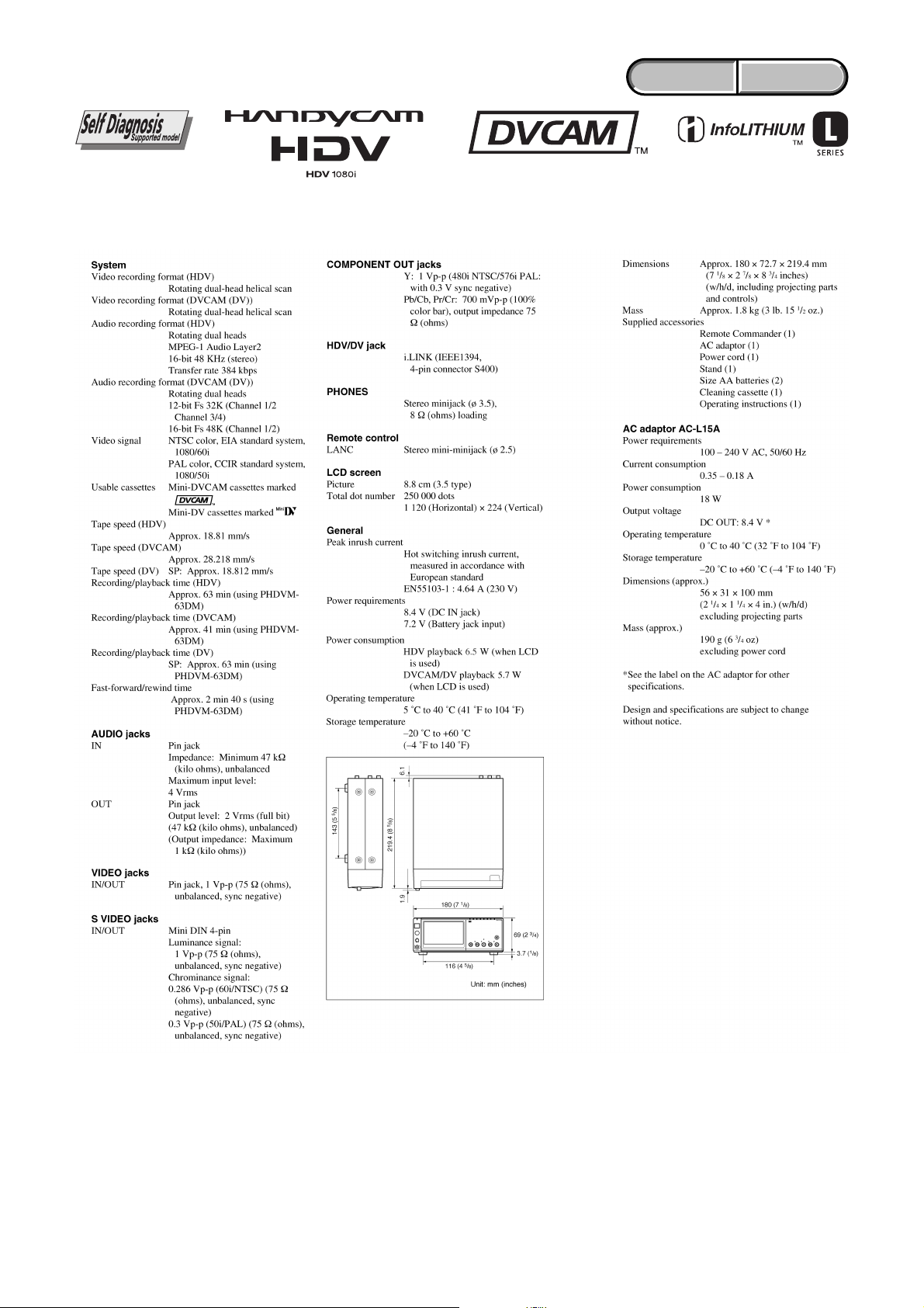
SPECIFICATIONS
SPECIFICATIONS
SERVICE NOTE
SERVICE NOTE
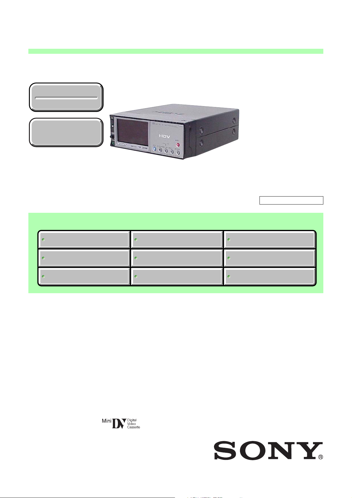
Photo : HVR-M10E
BLOCK DIAGRAMS
BLOCK DIAGRAMS
FRAME SCHEMATIC DIAGRAMS
FRAME SCHEMATIC DIAGRAMS
HVR-M10E
AEP Model
HVR-M10C
Chinese Model
HVR-M10N/M10P
E Model
HVR-M10J
Japanese Model
Z (Z311) MECHANISM
PRINTED WIRING BOARDS
PRINTED WIRING BOARDS
REPAIR PARTS LIST
REPAIR PARTS LIST
DISASSEMBLY
DISASSEMBLY
• INSTRUCTION MANUAL is shown at the end of this document.
• Reference number search on printed wiring boards is available.
• TO TAKE OUT A CASSETTE WHEN NOT EJECT (FORCE EJECT)
SCHEMATIC DIAGRAMS ADJUSTMENT
SCHEMATIC DIAGRAMS
DIGITAL HD VIDEOCASSETTE RECORDER
ADJUSTMENT
HVR-M10C/M10E/M10J/M10N/M10P/M10U
9-876-852-11
Sony EMCS Co.
2006J1600-1
©2006.10
Published by Kohda TEC
SPECIFICATIONS
ENGLISH JAPANESE
ENGLISH JAPANESE
HVR-M10C/M10E/M10J/M10N/M10P/M10U
— 2 —
ENGLISH JAPANESE
ENGLISH JAPANESE
HVR-M10C/M10E/M10J/M10N/M10P/M10U
— 3 —

SAFETY CHECK-OUT
After correcting the original service problem, perform the following
safety checks before releasing the set to the customer.
ENGLISH JAPANESE
ENGLISH JAPANESE
1. Check the area of your repair for unsoldered or poorly-soldered
connections. Check the entire board surface for solder splashes
and bridges.
2. Check the interboard wiring to ensure that no wires are
"pinched" or contact high-wattage resistors.
3. Look for unauthorized replacement parts, particularly
transistors, that were installed during a previous repair. Point
them out to the customer and recommend their replacement.
4. Look for parts which, through functioning, show obvious signs
of deterioration. Point them out to the customer and
recommend their replacement.
5. Check the B+ voltage to see it is at the values specified.
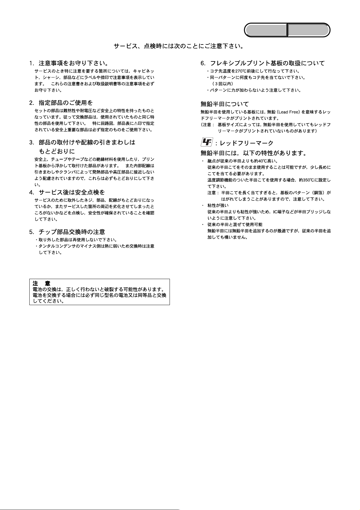
6. Flexible Circuit Board Repairing
• Keep the temperature of the soldering iron around 270˚C
during repairing.
• Do not touch the soldering iron on the same conductor of the
circuit board (within 3 times).
• Be careful not to apply force on the conductor when soldering
or unsoldering.
SAFETY-RELATED COMPONENT WARNING!!
COMPONENTS IDENTIFIED BY MARK 0 OR DOTTED LINE WITH
MARK 0 ON THE SCHEMATIC DIAGRAMS AND IN THE PARTS
LIST ARE CRITICAL TO SAFE OPERATION. REPLACE THESE
COMPONENTS WITH SONY PARTS WHOSE PART NUMBERS
APPEAR AS SHOWN IN THIS MANUAL OR IN SUPPLEMENTS
PUBLISHED BY SONY.
Unleaded solder
Boards requiring use of unleaded solder are printed with the leadfree mark (LF) indicating the solder contains no lead.
(Caution: Some printed circuit boards may not come printed with
the lead free mark due to their particular size.)
: LEAD FREE MARK
Unleaded solder has the following characteristics.
• Unleaded solder melts at a temperature about 40°C higher than
ordinary solder.
Ordinary soldering irons can be used but the iron tip has to be
applied to the solder joint for a slightly longer time.
Soldering irons using a temperature regulator should be set to
about 350°C.
Caution: The printed pattern (copper foil) may peel away if the
heated tip is applied for too long, so be careful!
• Strong viscosity
Unleaded solder is more viscous (sticky, less prone to flow) than
ordinary solder so use caution not to let solder bridges occur such
as on IC pins, etc.
• Usable with ordinary solder
It is best to use only unleaded solder but unleaded solder may
also be added to ordinary solder.
ATTENTION AU COMPOSANT AYANT RAPPORT
À LA SÉCURITÉ!
LES COMPOSANTS IDENTIFÉS PAR UNE MARQUE 0 SUR LES
DIAGRAMMES SCHÉMATIQUES ET LA LISTE DES PIÈCES SONT
CRITIQUES POUR LA SÉCURITÉ DE FONCTIONNEMENT. NE
REMPLACER CES COMPOSANTS QUE PAR DES PIÈSES SONY
DONT LES NUMÉROS SONT DONNÉS DANS CE MANUEL OU
DANS LES SUPPÉMENTS PUBLIÉS PAR SONY.
CAUTION :
Danger of explosion if battery is incorrectly replaced.
Replace only with the same or equivalent type.
HVR-M10C/M10E/M10J/M10N/M10P/M10U
— 4 —
ENGLISH JAPANESE
ENGLISH JAPANESE
HVR-M10C/M10E/M10J/M10N/M10P/M10U
— 5 —

TABLE OF CONTENTS
1. SERVICE NOTE
1-1. SER VICE NOTE ····························································· 1-1
1. NOTE FOR REPAIR ······················································· 1-1
2. POWER SUPPLY DURING REPAIRS··························1-2
3. TO TAKE OUT A CASSETTE WHEN NOT EJECT
(FORCE EJECT) ····························································· 1-2
1-2. SELF-DIAGNOSIS FUNCTION····································1-3
1. SELF-DIAGNOSIS FUNCTION···································· 1-3
2. SELF-DIAGNOSIS DISPLAY ·······································1-3
3. SELF-DIAGNOSIS CODE TABLE································ 1-4
2. DISASSEMBLY
2-1. DISASSEMBLY ······························································ 2-1
2-2. SERVICE POSITION ·····················································2-7
2-3. CIRCUIT BOARDS LOCATION ································· 2-10
2-4. FLEXIBLE BOARDS LOCATION ······························2-11
3. BLOCK DIAGRAMS
3-1. OVERALL BLOCK DIAGRAM (1/5) ···························3-1
3-2. OVERALL BLOCK DIAGRAM (2/5) ···························3-3
3-3. OVERALL BLOCK DIAGRAM (3/5) ···························3-5
3-4. OVERALL BLOCK DIAGRAM (4/5) ···························3-7
3-5. OVERALL BLOCK DIAGRAM (5/5) ···························3-9
3-6. POWER BLOCK DIAGRAM (1/4)······························ 3-11
3-7. POWER BLOCK DIAGRAM (2/4)······························ 3-13
3-8. POWER BLOCK DIAGRAM (3/4)······························ 3-15
3-9. POWER BLOCK DIAGRAM (4/4)······························ 3-17
4. PRINTED WIRING BOARDS AND
SCHEMATIC DIAGRAMS
4-1. FRAME PRINTED WIRING BOARD (1/2)··················4-1
FRAME PRINTED WIRING BOARD (2/2)·················· 4-3
4-2. SCHEMATIC DIAGRAMS
• FP-230 FLEXIBLE (RELAY)
SCHEMATIC DIAGRAMS····························4-7
• FP-971 FLEXIBLE (RELAY)
SCHEMATIC DIAGRAMS····························4-9
• FP-976 FLEXIBLE (RELAY)
SCHEMATIC DIAGRAMS··························4-11
• FP-977 FLEXIBLE (RELAY)
SCHEMATIC DIAGRAMS··························4-13
• HP-139 (HP JACK)
SCHEMATIC DIAGRAMS··························4-16
• JL-001 (JACK)
SCHEMATIC DIAGRAMS··························4-15
• FP-090 FLEXIBLE (RELAY)
SCHEMATIC DIAGRAMS··························4-16
• FP-096 FLEXIBLE (RELAY)
SCHEMATIC DIAGRAMS··························4-16
• JU-001 (AV IN JA CK)
SCHEMATIC DIAGRAMS··························4-17
• FP-095 FLEXIBLE (RELAY)
SCHEMATIC DIAGRAMS··························4-18
• LI-073 (BATTERY)
SCHEMATIC DIAGRAMS··························4-17
• MR-048 (1/2) (REC/PB RF AMP)
SCHEMATIC DIAGRAMS··························4-19
• MR-048 (2/2) (DRUM/CAPSTAN/LOADING MOTOR
DRIVE)
SCHEMATIC DIAGRAMS··························4-21
• PD-222 (LCD DRIVER, TIMING GENERATOR)
SCHEMATIC DIAGRAMS··························4-23
• PW-129 (REMOTE COMMANDER RECEIVER)
SCHEMATIC DIAGRAMS··························4-25
• SW-436 (FUNCTION PANEL)
SCHEMATIC DIAGRAMS··························4-27
• VA-120 (1/4) (CONNECTOR)
SCHEMATIC DIAGRAMS ··························4-29
• FP-088 FLEXIBLE (RELAY)
SCHEMATIC DIAGRAMS ··························4-29
• FP-089 FLEXIBLE (RELAY)
SCHEMATIC DIAGRAMS ··························4-29
• FFC-093 (RELAY)
SCHEMATIC DIAGRAMS ··························4-30
• VA-120 (2/4) (VIDEO IN/OUT)
SCHEMATIC DIAGRAMS ··························4-31
• VA-120 (3/4) (VIDEO AMP)
SCHEMATIC DIAGRAMS ··························4-33
• VA-120 (4/4) (AUDIO IN/OUT)
SCHEMATIC DIAGRAMS ··························4-35
• DA-033 (DC/DC CONVERTER)
SCHEMATIC DIAGRAMS ··························4-37
• DB-018 (1/2) (DC IN, CHARGE)
SCHEMATIC DIAGRAMS ··························4-39
• DB-018 (2/2) (DC/DC CONVERTER)
SCHEMATIC DIAGRAMS ··························4-41
• VC-367 (1/16) (BASE BAND PROCESS)
SCHEMATIC DIAGRAMS ··························4-43
• VC-367 (2/16) (OSD, D3 FILTER)
SCHEMATIC DIAGRAMS ··························4-45
• VC-367 (3/16) (HDV SIGNAL/RF SIGNAL PROCESS)
SCHEMATIC DIAGRAMS ··························4-47
• VC-367 (4/16) (HDV VIDEO DECODER)
SCHEMATIC DIAGRAMS ··························4-49
• VC-367 (5/16) (64MBIT Y/C-SDRAM)
SCHEMATIC DIAGRAMS ··························4-51
• VC-367 (6/16) (ILINK INTERFACE)
SCHEMATIC DIAGRAMS ··························4-53
• VC-367 (7/16) (DV/RF SIGNAL PROCESS)
SCHEMATIC DIAGRAMS ··························4-55
• VC-367 (8/16) (VIDEO A/D CONV.)
SCHEMATIC DIAGRAMS ··························4-57
• VC-367 (9/16) (HDV AUDIO SIGNAL PROCESS)
SCHEMATIC DIAGRAMS ··························4-59
• VC-367 (10/16) (AUDIO INPUT SELECT, AUDIO
CONVERTER)
SCHEMATIC DIAGRAMS ··························4-61
• VC-367 (11/16) (DS CONTROL)
SCHEMATIC DIAGRAMS ··························4-63
• VC-367 (12/16) (FRONT CONTROL)
SCHEMATIC DIAGRAMS ··························4-65
• VC-367 (13/16) (LSI CONTROL)
SCHEMATIC DIAGRAMS ··························4-67
• VC-367 (14/16) (MECHA CONTROL)
SCHEMATIC DIAGRAMS ··························4-69
• VC-367 (15/16) (CONNECTOR-1)
SCHEMATIC DIAGRAMS ··························4-71
• VC-367 (16/16) (CONNECTOR-2)
SCHEMATIC DIAGRAMS ··························4-73
• FP-228/FP-467/FP-826 FLEXIBLE
SCHEMATIC DIAGRAM ····························4-75
4-3. PRINTED WIRING BOARDS
• FP-230 FLEXIBLE (RELAY)
PRINTED WIRING BOARD ·······················4-79
• FP-971 FLEXIBLE (RELAY)
PRINTED WIRING BOARD ·······················4-81
• FP-976 FLEXIBLE (RELAY)
PRINTED WIRING BOARD ·······················4-81
• FP-977 FLEXIBLE (RELAY)
PRINTED WIRING BOARD ·······················4-83
• HP-139 (HP JACK)
PRINTED WIRING BOARD ·······················4-83
HVR-M10C/M10E/M10J/M10N/M10P/M10U
— 6 —

• JL-001 (JACK)
PRINTED WIRING BOARD ·······················4-85
• FP-090 FLEXIBLE (RELAY)
PRINTED WIRING BOARD ·······················4-85
• JU-001 (AV IN JA CK)
PRINTED WIRING BOARD ·······················4-87
• FP-095 FLEXIBLE (RELAY)
PRINTED WIRING BOARD ·······················4-89
• LI-073 (BATTERY)
PRINTED WIRING BOARD ·······················4-89
• MR-048 (REC/PB RF AMP, DRUM/CAPSTAN/
LOADING MOTOR DRIVE)
PRINTED WIRING BOARD ·······················4-91
• PD-222 (LCD DRIVER, TIMING GENERATOR)
PRINTED WIRING BOARD ·······················4-95
• PW-129 (REMOTE COMMANDER RECEIVER)
PRINTED WIRING BOARD ·······················4-99
• SW-436 (FUNCTION PANEL)
PRINTED WIRING BOARD ·····················4-101
• VA-120 (CONNECTOR, VIDEO IN/OUT, VIDEO AMP,
AUDIO IN/OUT)
PRINTED WIRING BOARD ·····················4-105
• FP-088 FLEXIBLE (RELAY)
PRINTED WIRING BOARD ·····················4-109
• FP-089 FLEXIBLE (RELAY)
PRINTED WIRING BOARD ·····················4-109
• DA-033 (DC/DC CONVERTER)
PRINTED WIRING BOARD ·····················4-113
• DB-018 (DC IN, CHARGE, DC/DC CONVERTER)
PRINTED WIRING BOARD ·····················4-115
• VC-367 (BASE BAND PROCESS, OSD, D3 FILTER,
HDV SIGNAL/RF SIGNAL PROCESS, HDV VIDEO
DECODER, 64MBIT Y/C-SDRAM, ILINK INTERFACE,
DV/RF SIGN AL PROCESS, VIDEO A/D CONV., HDV
AUDIO SIGNAL PROCESS, AUDIO INPUT SELECT ,
AUDIO CONVERTER, DS CONTROL, FRONT
CONTROL, LSI CONTROL, MECHA CONTROL,
CONNECTOR-1, CONNECTOR-2)
PRINTED WIRING BOARD ·····················4-119
• FP-228/FP-467/FP-826 FLEXIBLE
PRINTED WIRING BOARD ·····················4-123
4-4. WAVEFORMS ····························································4-125
4-5. MOUNTED PARTS LOCATION ······························· 4-128
5. REPAIR PARTS LIST
5-1-1.OVERALL SECTION····················································· 5-3
5-1-2.FRONT PANEL SECTION ············································· 5-4
5-1-3.CONTROL PANEL SECTION ·······································5-5
5-1-4.MAIN FRAME SECTION-1 ··········································5-6
5-1-5.MAIN FRAME SECTION-2 ··········································5-7
5-1-6.REAR PANEL SECTION··············································· 5-8
5-1-7.MECHANISM DECK OVERALL (Z311) ·····················5-9
5-1-8.LS CHASSIS BLOCK ASSEMBLY·····························5-10
5-1-9.MECHANICAL CHASSIS BLOCK ASSEMBLY·······5-11
Checking supplied accessories ················································ 5-12
5-2. ELECTRICAL PARTS LIST ········································ 5-14
6. ADJUSTMENTS
1. Before starting adjustment··············································· 6-1
1-1.
Adjusting items when replacing main parts and boards···
6-1. MECHANISM SECTION ADJUSTMENT····················6-3
1-1. Preparations for Check, Adjustment and Replacement of
Mechanism Block····························································6-3
1-1-1.Cassette Compartment Assy, Damper Assy ····················6-3
1-2. Periodic Inspection and Maintenance
6-2
1-2-1.Rotary Drum Cleaning ···················································· 6-4
1-2-2.Tape Path System Cleaning (Refer to Fig. 6-1-2.) ·········· 6-4
1-2-3.Periodic Inspection List ··················································· 6-5
1-2-4.Mode Selector II Operating Procedure····························6-6
2-4-1.Introduction ····································································· 6-6
2-4-2.Operation ·········································································6-7
2-4-3.Mechanism Status (Position) Transition Table Using
Mode Selector II ······························································ 6-9
2-4-4.Battery Alarm Indication ·················································6-9
1-3. Check, Adjustment and Replacement of
Mechanical Parts ··························································· 6-10
1-3-1.Flowchart of Replacement of Mechanical Parts············ 6-10
1-3-2.Drum··············································································6-11
1-3-3.Cassette Compartment Assy··········································6-13
1-3-4.TG7 Support ··································································6-14
1-3-5.Motor Holder Block Assy and L Motor Block Assy ····· 6-15
1-3-6.MIC Terminal (MIC902)···············································6-16
1-3-7.LED (D901)···································································6-17
1-3-8.Retainer Plate ································································6-18
1-3-9.T Reel Table Assy·························································· 6-19
1-3-10. Brake (S) and Release Rack (S)·································· 6-20
1-3-11. Band Adjuster, S Reel Table Assy and
TG2 Arm Block Assy ·················································6-21
1-3-12. ULE Brake Assy ·························································6-22
1-3-13. Cassette Positioning (S) ·············································· 6-23
1-3-14. TG7 Arm Block Assy and Pinch Arm Assy ················ 6-24
1-3-15. TG7 ·············································································6-25
1-3-16. Gooseneck Gear Assy ················································· 6-26
1-3-17. LS Guide Retainer and LS Cam Plate ························ 6-27
1-3-18. LS Chassis Block Assy and
Mechanical Chassis Block Assy································· 6-28
1-3-19. Brake (T) Block Assy ·················································6-30
1-3-20. END Sensor (Q901)····················································6-31
1-3-21. TOP Sensor (Q902)·····················································6-32
1-3-22. C-IN Switch (S903), S Reel Sensor (H901) and
T Reel Sensor (H902)····················································6-33
1-3-23. Guide Rail ··································································· 6-34
1-3-24. Conversion Gear ·························································6-35
1-3-25. Coaster (S) Block Assy and
Coaster (T) Block Assy ··············································6-36
1-3-26. TG5 Roller Assy and GL Gear (T) ····························· 6-37
1-3-27. TG2 Cam Plate Assy (N) ············································ 6-38
1-3-28. LS Arm Assy ·······························································6-39
1-3-29. M Slider Assy (1)························································ 6-40
1-3-30. M Slider Assy (2)························································ 6-41
1-3-31. EJ Arm ········································································6-42
1-3-32. Cam Gear and GL Driving·········································· 6-43
1-3-33. Rotary Encoder (S902) ··············································· 6-44
1-3-34. FP-228 Flexible Board (DEW SENSOR) and
FP-467 Flexible Board ··············································· 6-45
1-4. Adjustment ···································································· 6-46
1-4-1.FWD Position Adjustment·············································6-46
1-4-2.Reel Torque Check ························································6-46
1-4-3.LS Cam Plate Position Adjustment ·······························6-47
1-4-4.Tape Path Adjustment···················································· 6-48
6-2. VIDEO SECTION ADJUSTMENT································6-4
2-1. PREPARATIONS BEFORE ADJUSTMENTS ············ 6-52
2-1-1.Equipment to Required··················································6-52
2-1-2.Precautions on Adjusting··············································· 6-53
2-1-3.Adjusting Connectors ····················································6-54
2-1-4.Connecting the Equipment ············································6-54
2-1-5.Alignment Tapes···························································· 6-55
2-1-6.Input/Output Level and Impedance ······························· 6-55
2-2. INITIALIZATION OF 8, 9, A, B, C, D, 13, 18, 1A,
1B, 1C, 1D PAGE DATA···············································6-56
2-2-1.INITIALIZATION OF A, B, D, 1A, 1B PAGE DATA··6-56
1. Initializing the A, B, D, 1A, 1B Page Data ···················6-56
HVR-M10C/M10E/M10J/M10N/M10P/M10U
— 7 —

2. Modification of A, B, D, 1A, 1B Page Data··················6-56
3. A Page Table ·································································· 6-56
4. B Page Table ··································································6-57
5. D Page Table ·································································· 6-57
6. 1A Page Table ································································ 6-57
7. 1B Page Table ································································6-57
2-2-2.
INITIALIZATION OF 8, C, 13, 18, 1C PAGE DATA ···
1. Initializing the 8, C, 13, 18, 1C Page Data ···················· 6-58
2. Modification of 8, C, 13, 18, 1C Page Data ··················6-58
3. 8 Page Table ···································································6-59
4. C Page Table ··································································6-59
5. 13 Page Table································································· 6-60
6. 18 Page Table································································· 6-61
7. 1C Page Table ································································6-61
2-2-3.INITIALIZATION OF 9, 1D PAGE DATA ·················· 6-62
1. Initializing the 9, 1D Page Data ···································· 6-62
2. Modification of 9, 1D Page Data··································· 6-62
3. 9 Page Table ···································································6-62
4. 1D Page Table ································································ 6-62
2-3. SYSTEM CONTROL SYSTEM ADJUSTMENT ········ 6-63
1. Serial No. Input ····························································· 6-63
2-4. SERVO AND RF SYSTEM ADJUSTMENT ···············6-65
1. Cap FG Duty Adjustment (VC-367 board) ···················6-65
2. Switching Position Adjustment (VC-367 board)···········6-65
3. Error Rate Check ···························································6-66
3-1. Preparations before adjustments····································6-66
3-2. Error Rate Check ···························································6-66
3-3. Processing after Completing Adjustments ···················· 6-66
2-5. VIDEO SYSTEM ADJUSTMENTS····························· 6-67
1. Origin Oscillation Check (VC-367 board) ····················6-67
2. S VIDEO OUT Y Level Adjustment (VC-367 board)··· 6-68
3. S VIDEO OUT Chroma Level Adjustment
(VC-367 board) ····························································· 6-68
4. VIDEO OUT Y, Chroma Level Check
(VC-367 board) ····························································· 6-69
5. COMPONENT OUTPUT Level Adjustment
(VC-367 board) ····························································· 6-70
6. E-E Level Check (VC-367 board)································· 6-71
2-6. AUDIO SYSTEM ADJUSTMENTS ···························· 6-72
1. Playback Level Check ···················································6-73
2. Overall Level Characteristics Check ····························· 6-73
3. E-E Audio Level Check ·················································6-73
2-7. LCD SYSTEM ADJUSTMENT ···································6-74
1. LCD Automatic Adjustment (PD-222 board) ················ 6-74
2. Contrast Adjustment (HD) (PD-222 board) ··················6-75
3. V COM Adjustment (PD-222 board) ····························6-75
4. Sample Hold Phase Adjustment (PD-222 board)·········· 6-76
5. Transmissive Mode White Balance Adjustment
(PD-222 board)······························································ 6-76
6. Reflective Mode White Balance Adjustment
(PD-222 board)······························································ 6-77
6-3. SER VICE MODE·························································· 6-78
3-1. ADJUSTMENT REMOTE COMMANDER ················ 6-78
1. Using the adjustment remote commander ····················· 6-78
2. Precautions upon using the adjustment remote
commander ····································································6-78
3-2. DATA PROCESS··························································· 6-79
3-3. SER VICE MODE·························································· 6-80
1. Setting the Test Mode ···················································· 6-80
2. Emergence Memory Address (Mechanism section)······6-80
2-1. EMG Code (Emergency Code) ····································· 6-80
2-2. MSW Code ···································································· 6-81
3. Bit value discrimination ················································ 6-82
4. Switch check (1) ···························································· 6-82
5. Switch check (2) ···························································· 6-82
6. Switch check (5) ···························································· 6-83
7. LED check ····································································· 6-83
6-58
8. Record of Use check (1) ················································ 6-84
9. Record of Use check (2) ················································ 6-84
10. Record of Self-diagnosis check ····································· 6-85
SELF-DIAGNOSIS CODE TABLE········································6-86
HVR-M10C/M10E/M10J/M10N/M10P/M10U
— 8 —
1. SERVICE NOTE
1-1. SERVICE NOTE
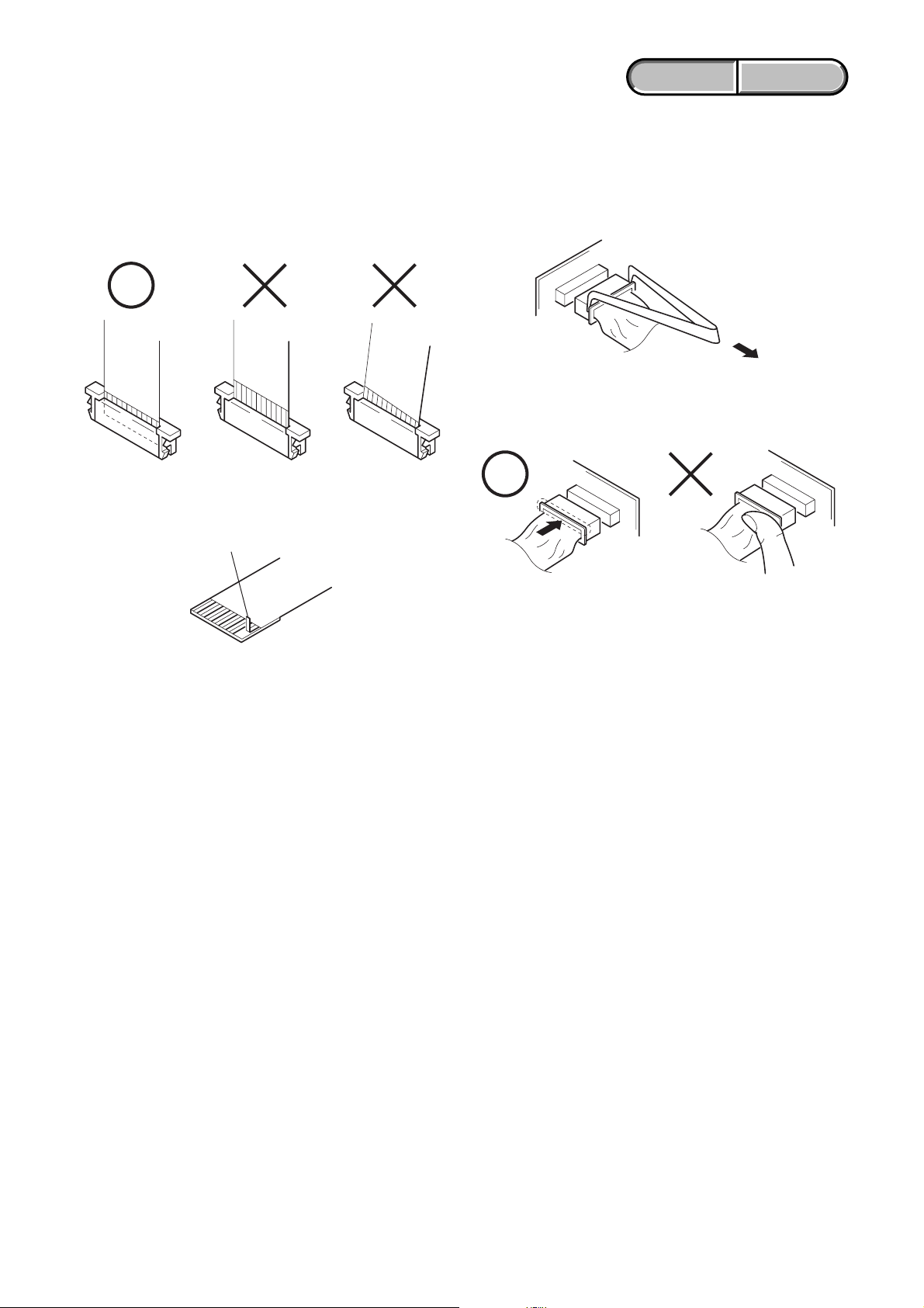
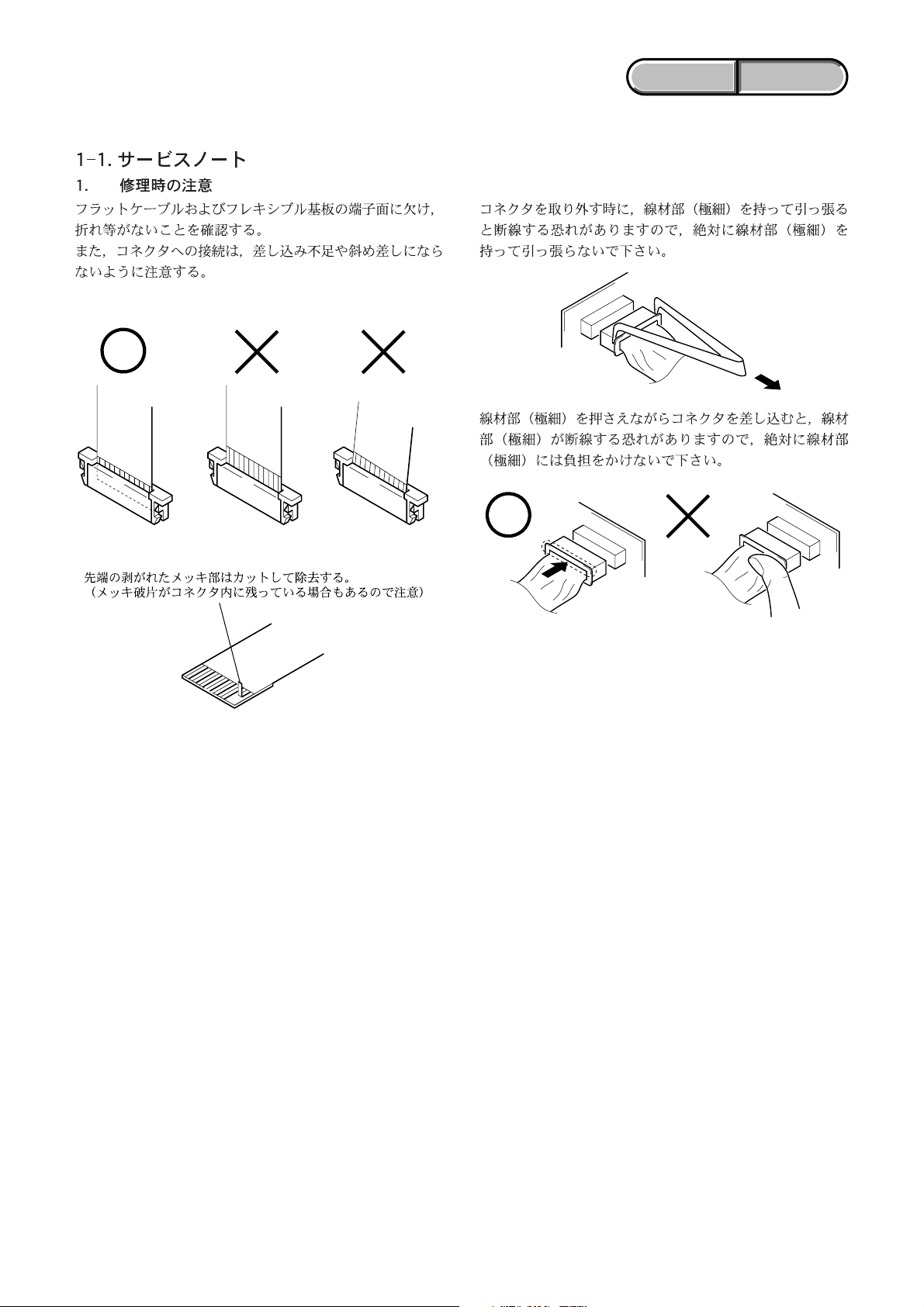
1. NOTE FOR REPAIR
Make sure that the flat cable and flexible board are not cracked of
bent at the terminal.
Do not insert the cable insufficiently nor crookedly.
Cut and remove the part of gilt
which comes off at the point.
(Take care that there are
some pieces of gilt left inside)
ENGLISH JAPANESE
ENGLISH JAPANESE
When remove a connector, don't pull at wire of connector.
Be in danger of the snapping of a wire.
When installing a connector, don't press down at wire of connector.
Be in danger of the snapping of a wire.
HVR-M10C/M10E/M10J/M10N/M10P/M10U
1-1
ENGLISH JAPANESE
ENGLISH JAPANESE
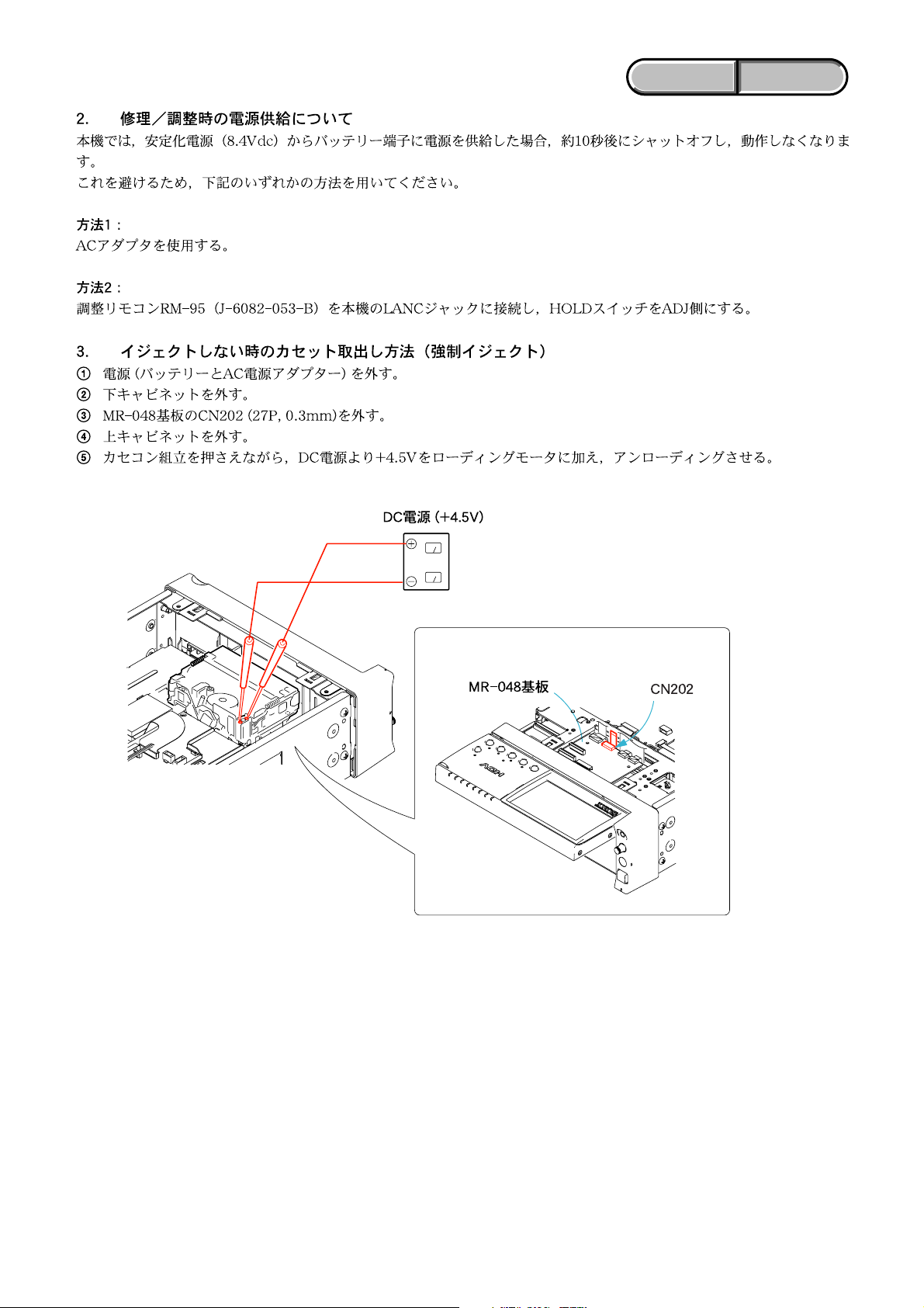
2. POWER SUPPLY DURING REPAIRS
In this unit, about 10 seconds after power is supplied to the battery terminal using the regulated power supply (8.4V),
the power is shut off so that the unit cannot operate.
This following two methods are available to prevent this.Take note of which to use during repairs.
Method 1.
Use the AC power adaptor.
Method 2.
Connect the servicing remote commander RM-95 (J-6082-053-B) to the LANC jack,and set the commander switch to the “ADJ” side.
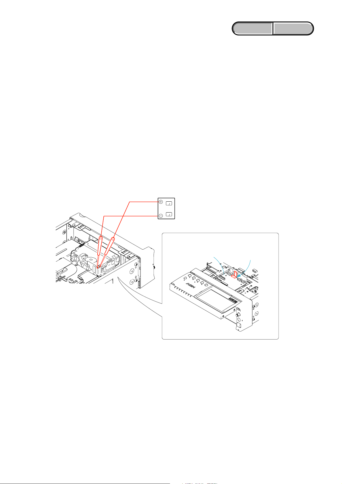
3. TO TAKE OUT A CASSETTE WHEN NOT EJECT (FORCE EJECT)
1 Remove the power supply (Battery and AC power adaptor).
2 Remove the bottom cabinet.
3 Disconnect the CN202 (27P, 0.3mm) of MR-048 board.
4 Remove the top cabinet.
5 Supply +4.5V from the DC power supply to the loading motor and unload with pressing the cassette compartment.
DC power supply
(+ 4.5V)
MR-048 board
CN202
HVR-M10C/M10E/M10J/M10N/M10P/M10U
1-2
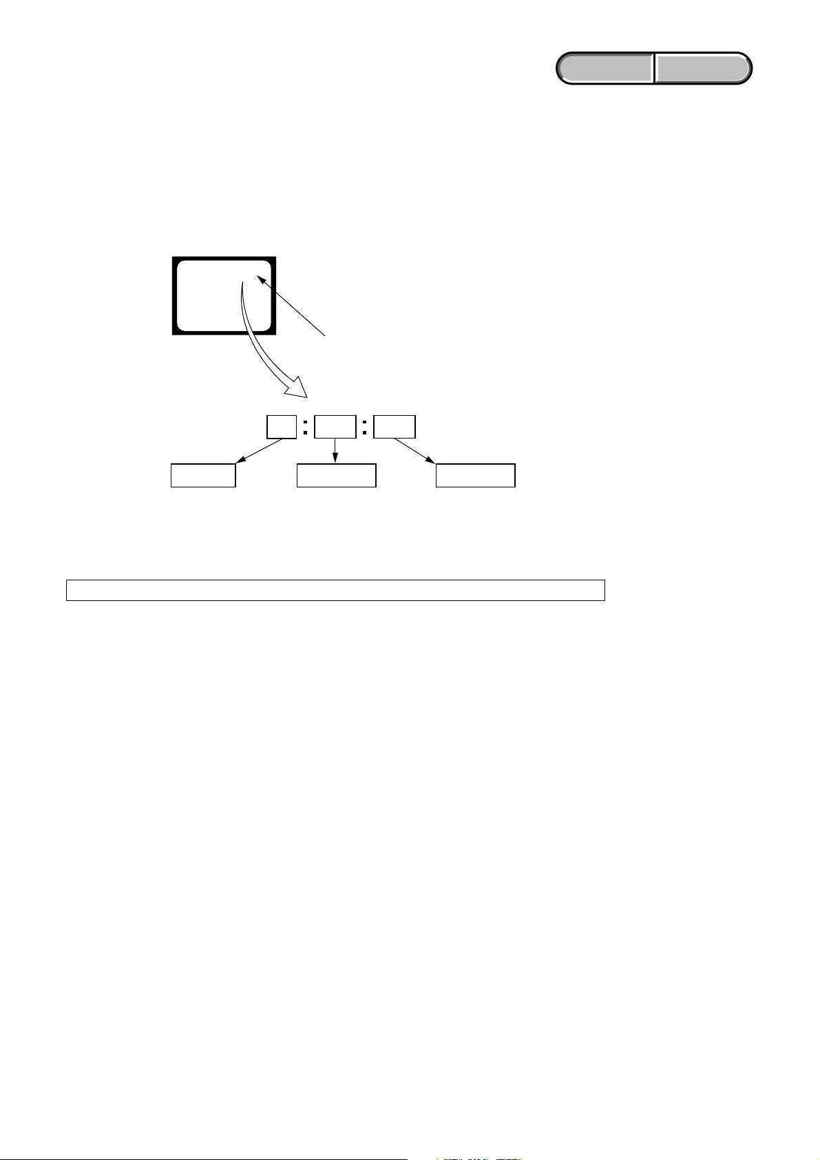
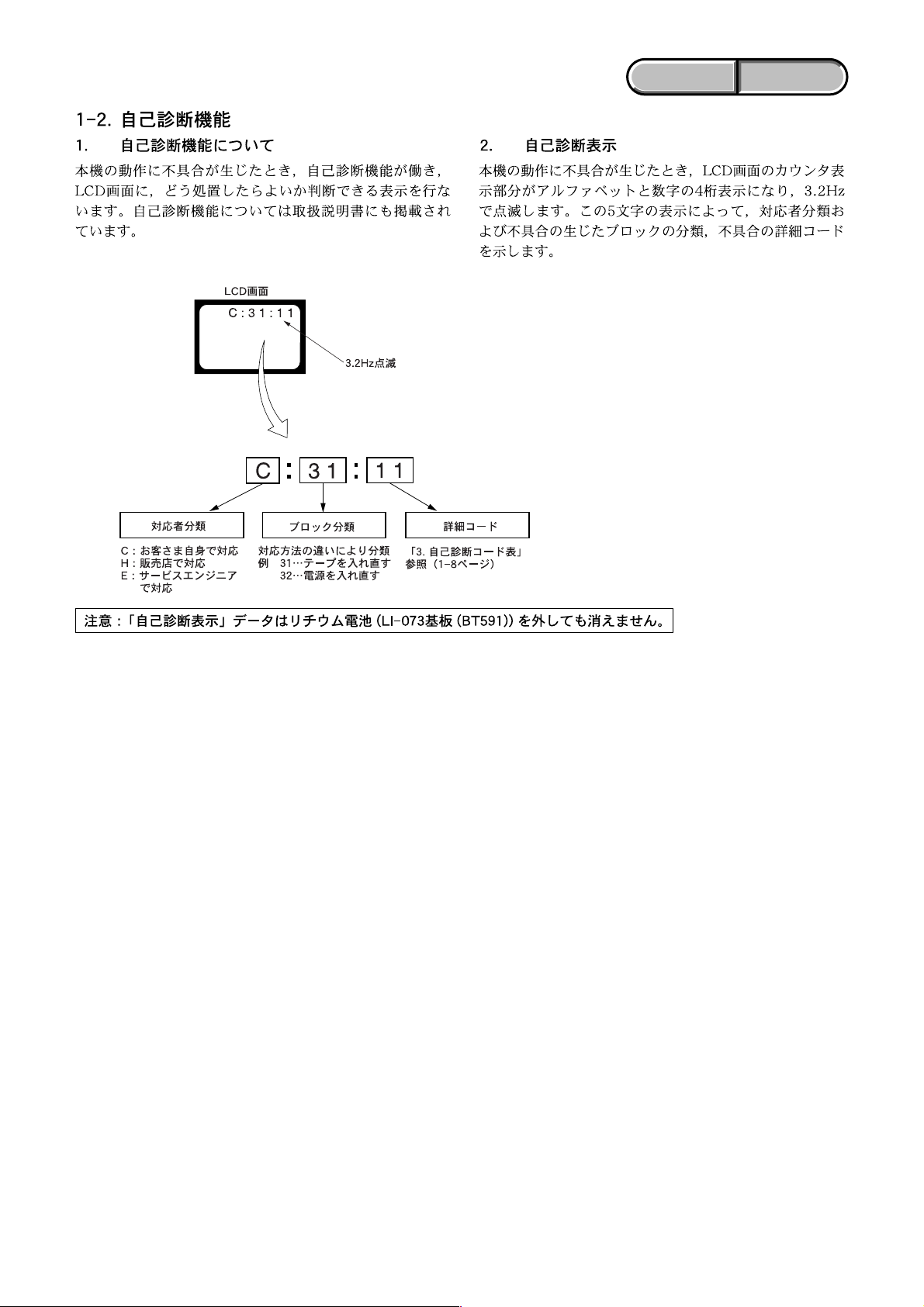
1-2. SELF-DIAGNOSIS FUNCTION
1. SELF-DIAGNOSIS FUNCTION
When problems occur while the unit is operating, the self-diagnosis
function starts working, and displays on the LCD screen what to do.
Details of the self-diagnosis functions are provided in the Instruction
manual.
LCD screen
C : 3 1 : 1 1
Blinks at 3.2Hz
ENGLISH JAPANESE
ENGLISH JAPANESE
2. SELF-DIAGNOSIS DISPLAY
When problems occur while the unit is operating, the counter of
the LCD screen consists of an alphabet and 4-digit number, which
blinks at 3.2Hz. This 5-character display indicates the “repaired
by:”, “block” in which the problem occurred, and “detailed code”
of the problem.
3 1C
Repaired by:
C : Corrected by customer
H : Corrected by dealer
E : Corrected by service
engineer
Note: The self-diagnosis display data will be kept even if the lithium battery (BT591 of LI-073 board) is removed.
Indicates the appropriate
step to be taken.
E.g.
31 ....Reload the tape.
32 ....Turn on power again.
Block
1 1
Detailed Code
Refer to page 1-4.
Self-diagnosis Code Table.
HVR-M10C/M10E/M10J/M10N/M10P/M10U
1-3
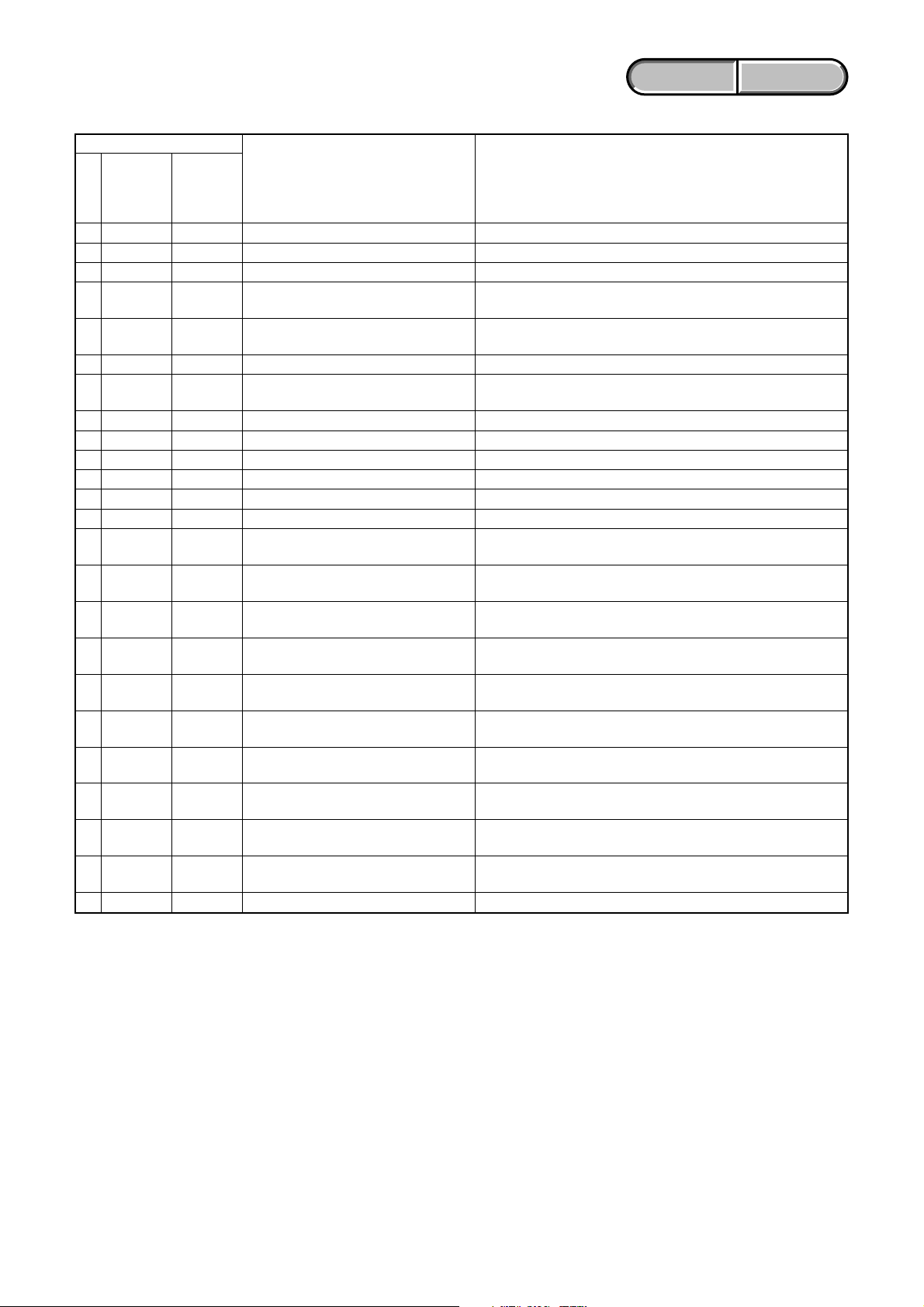
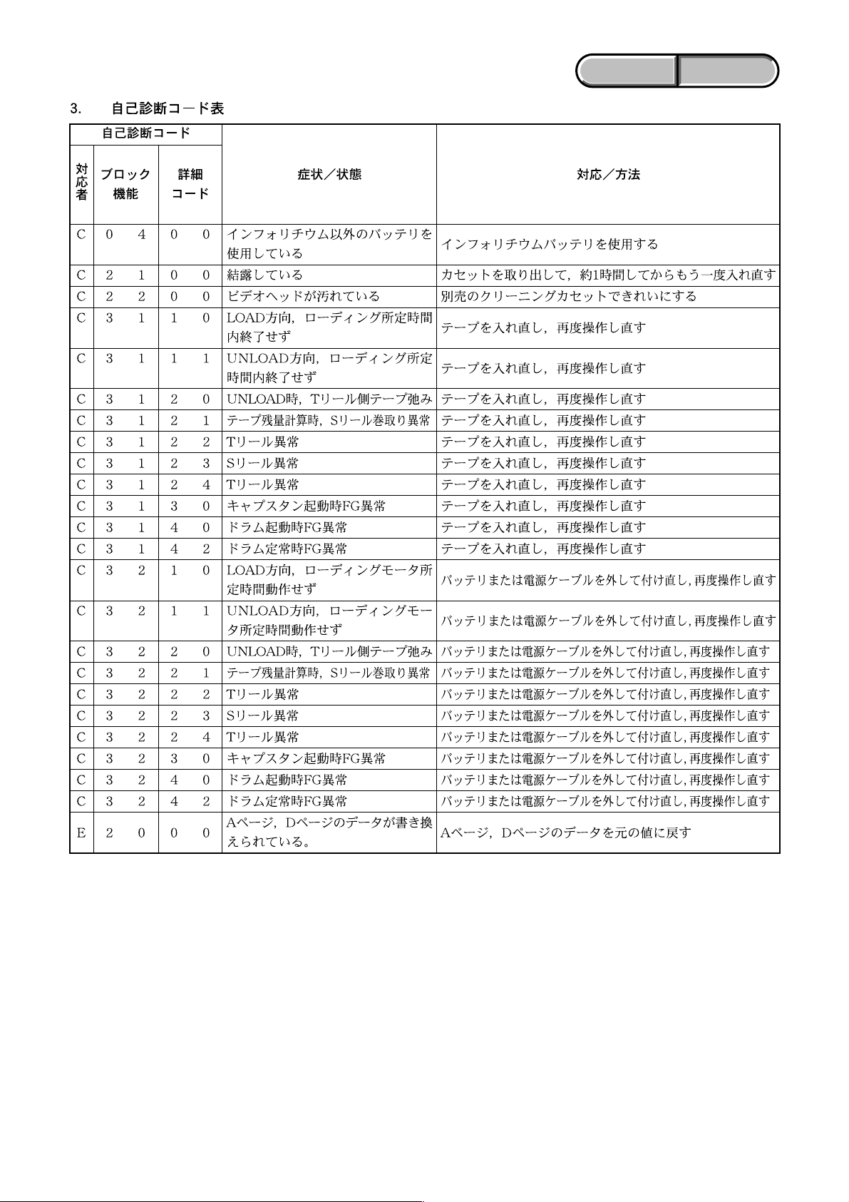
3. SELF-DIAGNOSIS CODE TABLE
Self-diagnosis Code
ENGLISH JAPANESE
ENGLISH JAPANESE
Function
Repaired by:
C
C
C
C
C
C
C
C
C
C
C
C
C
C
C
C
C
C
C
C
C
C
C
E
Block
04
21
22
31
31
31
31
31
31
31
31
31
31
32
32
32
32
32
32
32
32
32
32
20
Detailed
Code
00
00
00
10
11
20
21
22
23
24
30
40
42
10
11
20
21
22
23
24
30
40
42
00
Symptom/State
Non-standard battery is used.
Condensation.
Video head is dirty.
LOAD direction. Loading does not
complete within specified time
UNLOAD direction. Loading does not
complete within specified time
T reel side tape slacking when unloading
Winding S reel fault when counting the
rest of tape.
T reel fault.
S reel fault.
T reel fault.
FG fault when starting capstan.
FG fault when starting drum.
FG fault during normal drum operations.
LOAD direction loading motor time-
out.
UNLOAD direction loading motor
time-out.
T reel side tape slacking when
unloading.
Winding S reel fault when counting the
rest of tape.
T reel fault.
S reel fault.
T reel fault.
FG fault when starting capstan.
FG fault when starting drum
FG fault during normal drum
operations
Data on A page or D page are rewriten.
Correction
Use the info LITHIUM battery.
Remove the cassette, and insert it again after one hour.
Clean with the optional cleaning cassette.
Load the tape again, and perform operations from the beginning.
Load the tape again, and perform operations from the beginning.
.
Load the tape again, and perform operations from the beginning.
Load the tape again, and perform operations from the beginning.
Load the tape again, and perform operations from the beginning.
Load the tape again, and perform operations from the beginning.
Load the tape again, and perform operations from the beginning.
Load the tape again, and perform operations from the beginning.
Load the tape again, and perform operations from the beginning.
Load the tape again, and perform operations from the beginning.
Remove the battery or power cable, connect, and perform
operations from the beginning.
Remove the battery or power cable, connect, and perform
operations from the beginning.
Remove the battery or power cable, connect, and perform
operations from the beginning.
Remove the battery or power cable, connect, and perform
operations from the beginning.
Remove the battery or power cable, connect, and perform
operations from the beginning.
Remove the battery or power cable, connect, and perform
operations from the beginning.
Remove the battery or power cable, connect, and perform
operations from the beginning.
Remove the battery or power cable, connect, and perform
operations from the beginning.
Remove the battery or power cable, connect, and perform
operations from the beginning.
Remove the battery or power cable, connect, and perform
operations from the beginning.
Make data A page and D page correct value.
HVR-M10C/M10E/M10J/M10N/M10P/M10U
1-4
1. SERVICE NOTE
ENGLISH JAPANESE
ENGLISH JAPANESE
HVR-M10C/M10E/M10J/M10N/M10P/M10U
1-5
ENGLISH JAPANESE
ENGLISH JAPANESE
HVR-M10C/M10E/M10J/M10N/M10P/M10U
1-6
ENGLISH JAPANESE
ENGLISH JAPANESE
✂✂
HVR-M10C/M10E/M10J/M10N/M10P/M10U
1-7
ENGLISH JAPANESE
ENGLISH JAPANESE
HVR-M10C/M10E/M10J/M10N/M10P/M10U
1-8E
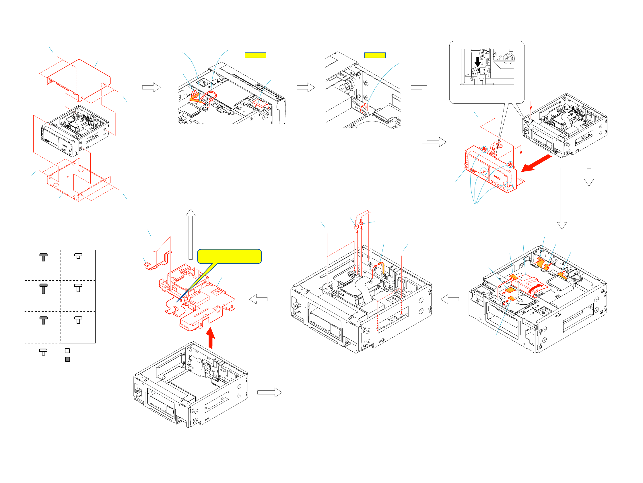
2. DISASSEMBLY
The following flow chart shows the disassembly procedure.
2-1. DISASSEMBLY
2
A
5
A
Screw
M3x6
2-059-756-01
C
A
6
Two screws (M3×6)
1
2
Two screws (M3×6)
3
Cabinet (upper)
4
Two screws (M3×6)
5
Two screws (M3×6)
6
Cabinet (lower)
B
M1.4x1.5
3-059-718-01
D
Screw
3
A
1
A
4
1
I
2
2
1
1
Open the clamper
2
FFC-094 Flexible flat cable (8P)
3
Harness (HP-146)
4
FFC-093 Flexible flat cable (50P)
Main frame section-1 (See page 2-3)
A
1
Three screws (M2x3) silver
2
Ground plate (HP)
3
Main frame section
Note:
Be very careful not to
damage the flexible board.
3
Ver 1.2 2005. 09
3
HELP 01 HELP 02
1
4
a
1
I
1
Open the clamper
a
3
B
Front panel section
2
4
2
3
D
1
5
D
1
Three screws (M2x3) silver
2
Four claws
3
Front panel section
7
1
3
4
(See page 2-5)
6
5
Screw
M3x8
3-077-331-41
Screw
M3x6
3-077-331-21
EF
Tapping screw
M2x5
3-080-206-21
I
Screw
M2x3
3-080-202-21
Screw
M2x5
7-681-000-00
Silver
Black
C
Main frame section-2 (See page 2-5)
1
FFC-095 Flexible flat cable (6P)
2
Battery terminal board (4P)
3
DC-IN connector (3P)
4
Two screws (M3x6) silver
5
Two screws (M3x6) silver
2
1
Peel the sheet (SW-VA)
2
FP-230 flexible board (22P)
3
FP-230 flexible board (30P)
4
FP-098 flexible board (28P)
5
FP-090 flexible board (10P)
6
FP-096 flexible board (12P)
7
FP-095 flexible board (28P)
HVR-M10C/M10E/M10J/M10N/M10P/M10U
2-1 2-2
2. DISASSEMBLY
2. DISASSEMBLY
Ver 1.1 2005. 05
3
1
Screw (M2x3) silver
2
FP-230 flexible board (51P)
3
Three screws (M2x3) silver
4
VC connector retainer
5
FP-971 flexible board (100P),(100P)
6
FP-096 flexible board (12P)
7
FP-090 flexible board (10P)
8
Five screws (M2x3) silver
9
VA-120 board
A
8
I
I
4
6
5
3
I
1
HELP 03
VC-367
2
6
VA-120
9
4
VC-367
7
1
FP-089 flexible board (33P)
2
FP-088 flexible board (39P)
3
Five screws (M2x3) silver
4
FP-976 flexible board (80P)
5
FP-976 flexible board (80P)
6
VC-367 board
5
1
5
I
DB-018
7
DA-033
I
2
1
FP-098 flexible board (28P)
2
Two screws (M2x3) silver
3
DB connector retainer
4
FP-977 flexible board (100P)
5
Four screws (M2x3) silver
6
Board to board connector (28P)
7
DB-018 board
3
4
6
A
Screw
M3x6
2-059-756-01
C
Screw
M3x8
3-077-331-41
B
Screw
M1.4x1.5
3-059-718-01
D
Screw
M3x6
3-077-331-21
EF
Tapping screw
M2x5
3-080-206-21
I
Screw
M2x3
3-080-202-21
Screw
M2x5
7-681-000-00
Silver
Black
2
I
1
1
I
1
4
DA-033
3
2
Four screws (M2x3) silver
2
FP-976 flexible board (80P)
3
FP-976 flexible board (80P)
4
DA-033 board
HVR-M10C/M10E/M10J/M10N/M10P/M10U
2-3 2-4
2. DISASSEMBLY
2. DISASSEMBLY
3
2
F
4
1
E
6
7
B
Harness (HP-146)
1
2
Screw (M2x5) silver
3
Damper
4
Three tapping screws (M2x5) black
5
Screw (M2x3) silver
6
Front sub chassis
7
HP-139 board
I
5
1
a
1
Lean the control panel section
in the direction of an arrow a .
2
Two tapping screws (M2x5) black
3
Ground plate (R)
4
Dowel
5
E
3
5
b
4
2
Remove the control panel section
in the direction of an arrow b .
4
3
6
7
1
Tapping screw (M2x5) black
2
Fulcrum plate (front L)
3
Damper
4
Front panel assembly
5
FFC-094 Flexible flat cable (8P)
6
(Power) button
7
(HP VOL) knob
8
PW-129 board
8
5
2
E
1
A
Screw
M3x6
2-059-756-01
C
Screw
M3x8
3-077-331-41
B
Screw
M1.4x1.5
3-059-718-01
D
Screw
M3x6
3-077-331-21
EF
Tapping screw
M2x5
3-080-206-21
I
Screw
M2x3
3-080-202-21
Screw
M2x5
7-681-000-00
Silver
Black
1
Three screws (M2x3) silver
2
Cover (MD)
3
Three screws (M2x3) silver
4
Mechanism deck,
MD frame assembly
1
1
I
2
Four screws (M2x3) silver
2
MR-048 board
3
Four screws (M1.4x1.5) silver
4
MD frame assembly
5
Mechanism deck
5
1
Three screws (M3x6) silver
2
Two screws (M3x6) silver
3
Side plate (L)
4
Two screws (M3x6) silver
5
Rear panel section
4
D
4
3
I
C
4
MR-048
B
3
2
5
3
D
1
D
2
I
HVR-M10C/M10E/M10J/M10N/M10P/M10U
1
2-5 2-6
2-2. SERVICE POSITION
2. DISASSEMBLY
2. DISASSEMBLY
2
A
3
A
1
A
5
A
6
4
[SERVICE POSITION TO
CHECK THE VTR SECTION]
Connection to Check the
VTR Section (page 2-9)
2
3
1
I
1
4
4
a
1
2
3
2
F
4
a
7
1
6
3
4
a
2
3
5
2
4
D
3
5
1
D
E
6
b
3
1
I
DA-033
1
E
3
2
1
4
5
I
2
3
4
I
3
2
DB-018
7
6
DA-033
7
I
5
3
I
1
8
I
1
I
3
1
I
2
4
6
5
3
VA-120
VC-367
9
2
6
4
7
VC-367
2
E
1
2
2
1
HVR-M10C/M10E/M10J/M10N/M10P/M10U
5
2
I
1
1
I
2
1
4
4
1
C
2
5
E
3
1
3
C
2
6
3
4
D
D
D
3
1
2
7
I
5
C
2
4
C
5
5
3
I
4
4
3
B
M
R
-0
4
8
2
1
I
2-7 2-8

2. DISASSEMBLY
2. DISASSEMBLY
[SERVICE POSITION TO CHECK THE VTR SECTION]
Connection to Check the VTR Section
To check the VTR section, set the VTR to the "Forced VTR power ON" mode.
Operate the VTR functions using the adjustment remote commander
(with the HOLD switch set in the OFF position).
Setting the “Forced VTR Power ON” mode
1) Select page: 0, address: 01, and set data: 01.
2) Select page: 0, address: 10, and set data: 00.
3) Select page: A, address: 10, set data: 02, and press
the PAUSE button of the adjustment remote commander.
Exiting the “Forced VTR Power ON” mode
1) Select page: 0, address: 01, and set data: 01.
2) Select page: 0, address: 10, and set data: 00.
3) Select page: A, address: 10, set data: 00, and press the
PAUSE button of the adjustment remote commander.
4) Select page: 0, address: 01, and set data: 00.
*1: Only in the following cases, it is necessary to connect these flexible cables.
1) When ejecting the cassette.
2) When using the LCD block.
3) When changing the menu settings.
4) When checking the audio systems.
CPC-8 jig
(J-6082-388-A)
FP-098 flexible
board (28P)
Mechanism deck
FP-977 flexible
board (100P)
CN201
CN101
CN103
CN107
DB-018
CN205
CN104
AC IN
DC-IN connector
CN206
Extension cable (28P)
(J-6082-566-A)
AC power
adaptor
DC-IN
Monitor TV
CN0102
CN0103
FP-098 flexible
board (28P)
CN203
CN202
CN201
CN104
MR-048
FP-230 flexible
board (51P)
CN0101
FP-230 flexible
board (22P)
FP-230 flexible
board (30P)
1*
FFC-093 Flexible flat cable (50P)
CN0007
FP-977 flexible
board (100P)
CN0003
CN0005
CN0001
CN2007
DA-033
FP-976 flexible
board (80P)
1*
CN0008
CN2005
VA-120
VA-120 board
CN2008
DA-033 board
CN0002
VC-367 board
VC-367
CN0004
CN2001
CN2000
CN2006
1*
CN801
CN901
JL-001 board
Adjustment remote
commander (RM-95)
FP-095 flexible board (30P)
FP-096 flexible board (12P)
Video
out jack
JU-001 board
HVR-M10C/M10E/M10J/M10N/M10P/M10U
2-9

2-3. CIRCUIT BOARDS LOCATION
2. DISASSEMBLY
2. DISASSEMBLY
PW-129
HP-139
VA-120
MR-048
PD-222
FP-977
DB-018
FP-976
LI-073
DA-033
JU-001
JL-001
VC-367
SW-436
NAME FUNCTION
DA-033
DB-018
FP-971
FP-976
FP-977
HP-139
JL-001
JU-001
LI-073
MR-048
PD-222
PW-129
SW-436
VA-120
VC-367
DC/DC CONVERTER
DC IN, CHARGE, DC/DC CONVERTER
RELAY
RELAY
RELAY
HP JACK
JACK
AV IN JACK
BATTERY
REC/PB RF AMP, DRUM/CAPSTAN/LOADING MOTOR DRIVE
LCD DRIVER, TIMING GENERATOR
REMOTE COMMANDER RECEIVER
FUNCTION PANEL
CONNECTOR, VIDEO IN/OUT, VIDEO AMP, AUDIO IN/OUT
BASE BAND PROCESS, OSD, D3 FILTER, HDV SIGNAL/RF SIGNAL PROCESS,
HDV VIDEO DECODER, 64MBIT Y/C-SDRAM, ILINK INTERFACE, DV/RF SIGNAL PROCESS
VIDEO A/D CONV., HDV AUDIO SIGNAL PROCESS, AUDIO INPUT SELECT,
AUDIO CONVERTER, DS CONTROL, FRONT CONTROL, LSI CONTROL,
MECHA CONTROL, CONNECTOR-1, CONNECTOR-2
FP-976
FP-971
HVR-M10C/M10E/M10J/M10N/M10P/M10U
2-10
2. DISASSEMBLY
5
2. DISASSEMBLY
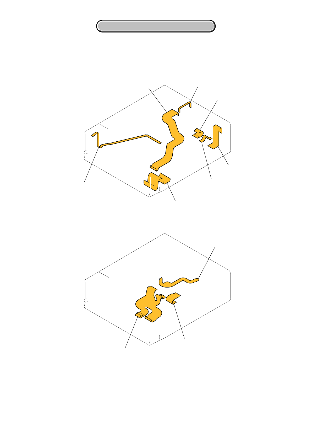
2-4. FLEXIBLE BOARDS LOCATION
The flexible boards contained in the mechanism deck and lens block are not shown.
FFC-094
FP-098
FFC-095
FP-089
FP-09
FP-096
FFC-093
FP-230
FP-090
FP-088
HVR-M10C/M10E/M10J/M10N/M10P/M10U
2-11E

HELP
)
Sheet attachment positions and procedures of processing the flexible boards/harnesses are shown.
HELP 01
FC-094 Flexible flat cable (8P)
Clamper
Harness (HP-146)
HELP 02
HELP 03
Harness (HP-146)
Main frame section
FC-094 Flexible flat cable (8P
Clamper
FP-098 flexible board
HVR-M10C/M10E/M10J/M10N/M10P/M10U
HELP
Link
Link
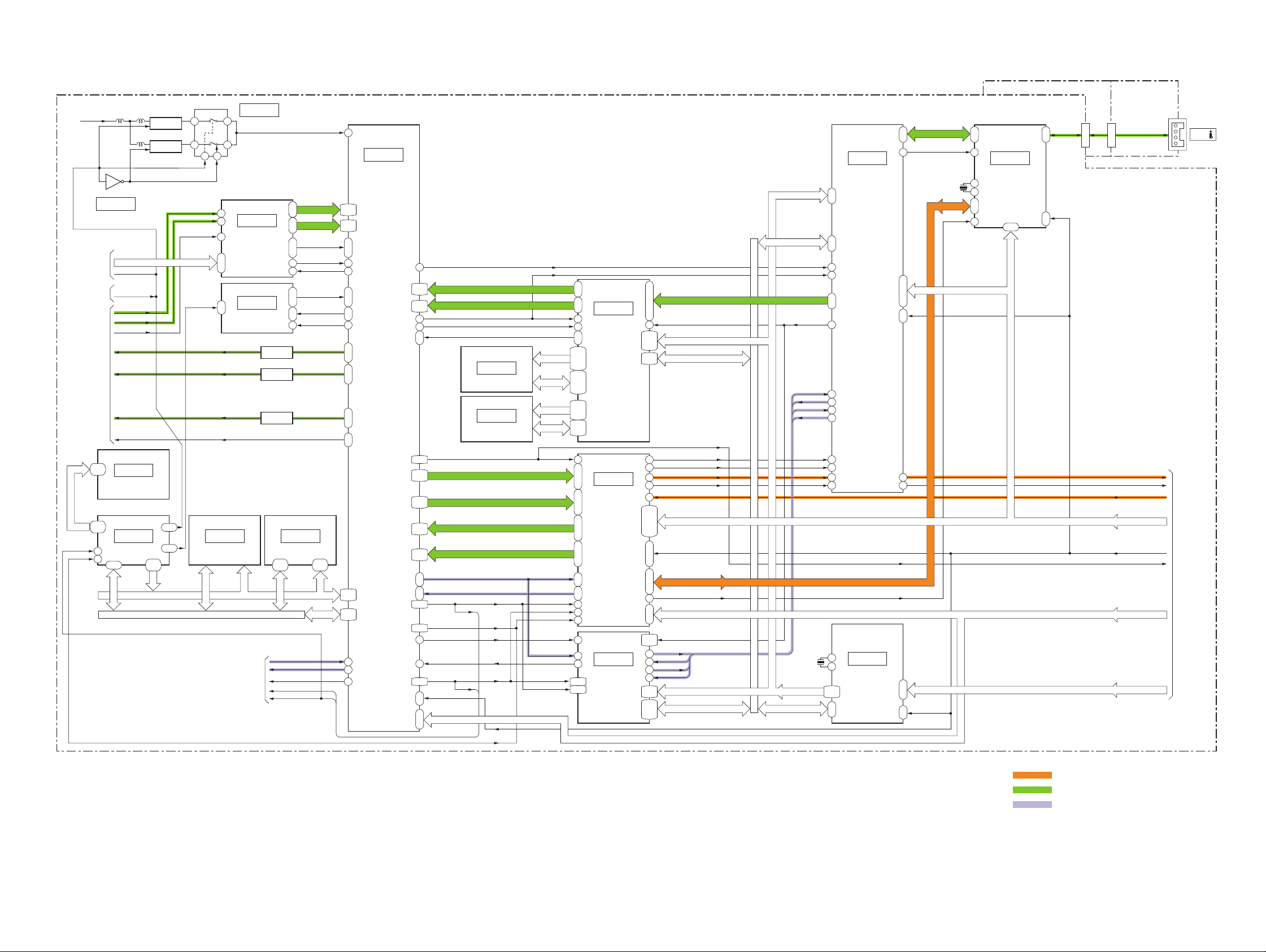
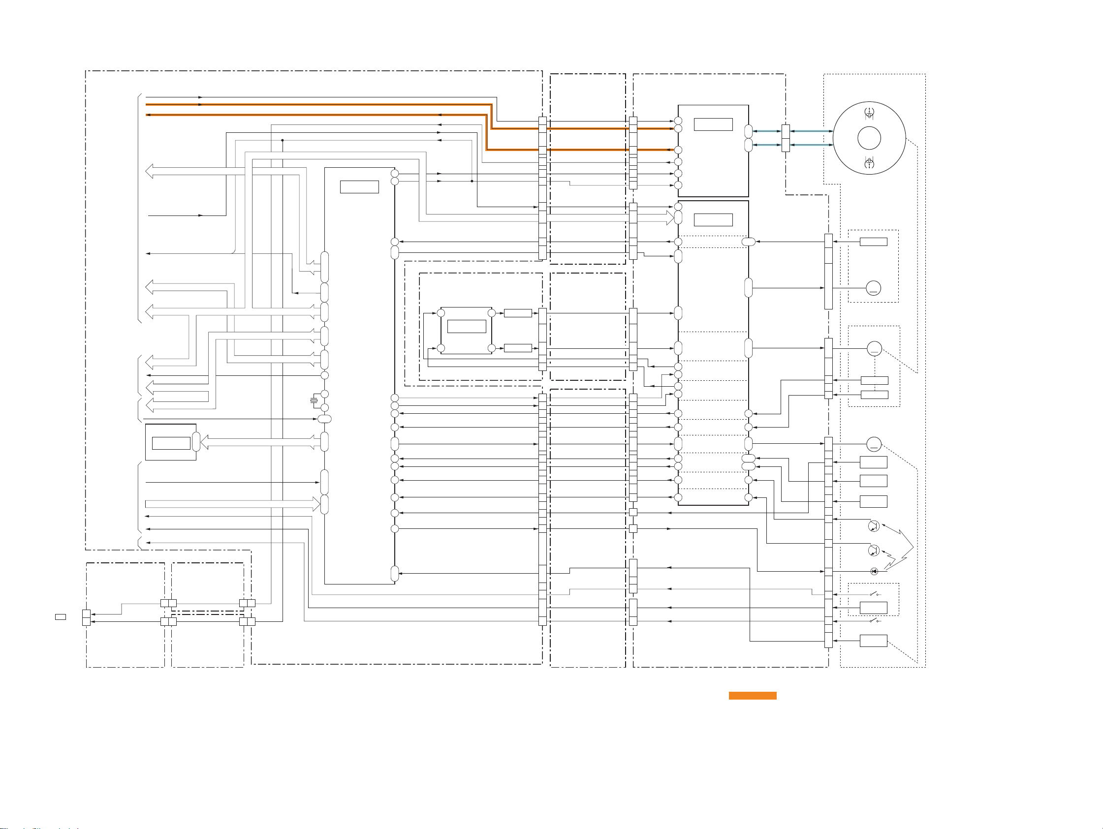
3. BLOCK DIAGRAMS
OVERALL BLOCK DIAGRAM (1/5)
OVERALL BLOCK DIAGRAM (1/5)
OVERALL BLOCK DIAGRAM (2/5)
OVERALL BLOCK DIAGRAM (2/5)
OVERALL BLOCK DIAGRAM (3/5)
OVERALL BLOCK DIAGRAM (3/5)
OVERALL BLOCK DIAGRAM (5/5)
OVERALL BLOCK DIAGRAM (5/5)
POWER BLOCK DIAGRAM (1/4)
POWER BLOCK DIAGRAM (1/4)
POWER BLOCK DIAGRAM (2/4)
POWER BLOCK DIAGRAM (2/4)
POWER BLOCK DIAGRAM (3/4)
POWER BLOCK DIAGRAM (3/4)
POWER BLOCK DIAGRAM (4/4)OVERALL BLOCK DIAGRAM (4/5)
POWER BLOCK DIAGRAM (4/4)OVERALL BLOCK DIAGRAM (4/5)
HVR-M10C/M10E/M10J/M10N/M10P/M10U
3. BLOCK DIAGRAMS
3-1. OVERALL BLOCK DIAGRAM (1/5)
6
2
6
25
64
•
66
•
63
3
•
1
FLASH
TO
OVERALL
BLOCK DIAGRAM
(2/5)
(PAGE 3-3)
(1/16)
IC2023
VCO
(8/16)
IC5001
VIDEO
A/D
CONV.
(2/16)
IC2101
OSD
Q2119-2121
Q2110-2112
LPF
Q2116-2117
BUFF
Q2113-2115
BUFF
IC8003
D0-D15 A1-A14
20-26
29-35
VC-367 BOARD (1/5)
D 2.28 V
NTSC/XPAL DET
(1/16)
IC2022
TO
OVERALL
1
BLOCK DIAGRAM
q;
2
(3/5)
(PAGE 3-5)
TO
OVERALL
BLOCK DIAGRAM
(4/5)
(PAGE 3-8)
TO
OVERALL
BLOCK DIAGRAM
(2/5)
(PAGE 3-3)
CKFSO
DSCK VM
103-105
235,236
NTSC/XPAL DET
NTSC/XPAL DET
Y
C
CK
YO
PRO
PBO
EVGR
EVBL
PLRE
PLGR
PLBL
XPHD
XPVD
(11/16)
1-3
5,6
IC8002
EEPROM
(11/16)
IC8009
D0-D15
16-35
CONTROL
DS
124
123
(1/2)
A1-A22
291-304
1-32
X2020
55.631MHz
X2021
55.687MHz
100,102
1 2
5
37
Y
C
CK
VD SO,SI,SCK
OSD SO
XOSD SCK
129
(11/16) (11/16)
IC8001
MEMORY
D0-D15 A1-A21
A1-A22
D0-D15
6
( ) : Number in parenthesis ( ) indicates the division number of schematic diagram where the component is located.
SPCKO
132
(1/16)
IC2021
BASE BAND
PROCESS
59
59
|
|
52
52
49
|
42
38
•
37
•
36
34
68
17
•
16
•
14
20
•
19
8
16Mbit
SDRAM
AUIN11
ADAO1
CK256FSO
CK64FSO
CKFSO
VFIY0-VFIY7
VFIC0-VFIC7
VFI HD
VFI VD
VFI OE
AFCK
CK13MFO
COLH1
COLH2
COLH3
HOSDHD
HOSDVD
CK14MFO
20-26
29-35
26-29
264-267
30-38
273-276
262
•
25
•
263
24
17
315
•
85
•
317
313
•
80
81
Y
PR
75
PB
•
79
•
77
EVGR
EVBL
72
•
74
PLRE
PLGR
68
PLBL
•
69
•
67
XPHD
XPVD
64
•
56
222-234
A2-A19
442-452
8-15
D0-D15
245-252
193
423
186
332
107-110
339-342
102-105
334-338
189
111
DHD
DFD
115
•
344
VY[0]-VY[7]
VC[0]-VC[7]
(5/16)
IC3201
Y SDRAM
(5/16)
IC3202
C SDRAM
22,20
45,46
283,285
43,44
281,282
53,290
291,292
51,52
288,289
187,188
55,54
195,198
418
•
197
419
•
201
17
419
254
255
257
•
258
•
19
RYO0-RYO3,DEHD,DEVD,DEFLD,SGOUT
RCO0-RCO3,EDHD,EDVD,EDFLD,FRMREF
RYI0-RYI3,DE0-DE3
RCI0-RCI3,DE4-DE7
ADATAIN0
ADATAIN1
ADATAOUT0
ADATAOUT1
CK64FSO
DSCK VM
AUIN21 AUIN21
FRRV
TRRT
VSP SO,SI,SCK
269
256
289
272
CK27MFO1
291
CK DENEBO2
252
287
286
42,44
47-49
52-55
A0-A10
61,64
3-24
33-35
58,59
D0-D31
68-90
123-124
134-137
A0-A10
144-147
151
92-118
148,150
D0-D31
155-176
VCK
143 86
119
162
120
163
121
122
123
166
124
125
168
127
167
126
CK64FSO
CKFSO
DSCK VM
CK13MFOCK13MFO
ADATAIN0
CKFSOCKFSO
43,73
CK64FSO
41,71
(20/25)
|
(4/16)
|
IC3001
HDV
VIDEO
DECORDER
•
66
61
(7/16)
•
•
IC4001
•
70
71
13
72
14
73
21
78
15
97
45
74
DV
SIGNAL
•
PROCESS
•
RF
•
SIGNAL
PROCESS
•
•
•
•
•
•
•
•
(9/16)
IC7001
HDV
AUDIO
SIGNAL
PROCESS
215
225
223
221
BS[0]-BS[7]
220
231
227
224
DJCLK
226
191,218
193-201
HADR[0]-HADR[13]
204-207
210-213
179-189
HDAT[0]-HDAT[7]
192
VIT DT
VIT CK
30
CREC DT
45
CREC CK
41
RF IN RF IN
139
107
54
•
•
189
152
•
•
153
55
MC BUS MC BUS
•
•
109
190
•
•
192
155
SWP
FRRV
60
TRRT
•
TRRV
58
•
112
•
111
149
•
186
•
LBUS0-LBUS3
150
•
187
TRCK0
104
114
•
157
VSP SO,SI,SCK
•
3
AUIN21
38,42
48,49
AUDAL
59
AUDAO
35
AUENI
60
AUENO
47
62,18
HADR[0]-HADR[3] HADR[0]-HADR[13]
39,46
58,69
81,95
HDAT[0]-HDAT[7] HDAT[0]-HDAT[7]
120,124
135,6
HADR[0]-HADR[7]
HDAT[0]-HDAT[7]
FLD27MFFLD27MF
CK27MFO1
CREC DT
CREC CK
X8601
20MHz
AUDAL
AUDAO
AUENI
AUENO
DJCLK
VIT DT
VIT CK
FP-090 FLEXIBLE BOARD
JL-001
BOARD(1/3)
FRRV
TRRT
TRRV
CN901
HDV/DV
SWP
VCK
3
TO
OVERALL
BLOCK DIAGRAM
(3/5)
(PAGE 3-5)
TPA
CN0009
NTPA
5
187
PD10-PD17
|
(3/16)
IC2502
HDV
SIGNAL
PROCESS
HDV
RF SIGNAL
241
PROCESS
|
251
256
|
266
7
1
11
|
23
10
276
279
277
281
71
72
73
74
197
185 87
LBUS0-LBUS3
204
|
207
MC BUS
213
|
224
FRRV
TRRT
235
229
REC DT
80
REC CK
82
24.576MHz
X3501
TRCK0
PCLK1
77
|
85
(6/16)
IC3501
iLINK
INTERFACE
149
150
95
|
98
104
51-64
TPB
139
NTPB
|
136
FRRV
TRRT
105
108
4
•
•
6
2
•
•
4
6
•
•
3
8
CN902
REC DT
REC CK
VSP SO,SI,SCK
(13/16)
1
IC8601
3
LSI
CONTROL
44-37
33-28
52
|
45
66
•
65
VSP2 SO,SI,SCK
•
63
FRRV
204
TRRT
•
203
VSP2 SO,SI,SCK
16
HVR-M10C/M10E/M10J/M10N/M10P/M10U
VIDEO/AUDIO SIGNAL
VIDEO SIGNAL
AUDIO SIGNAL
3-1 3-2
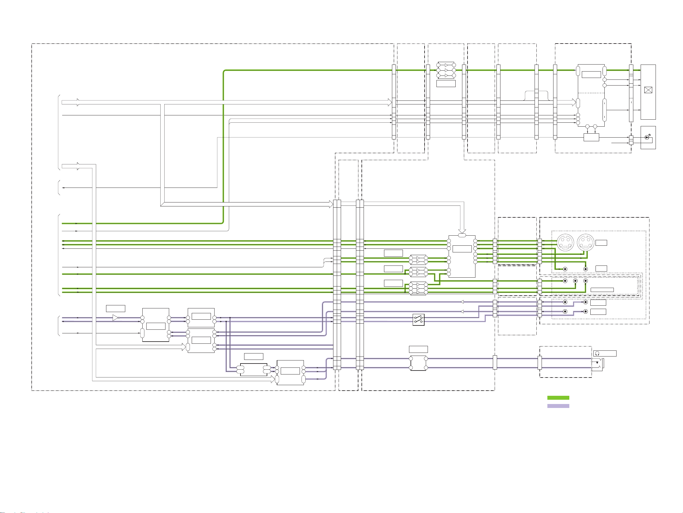
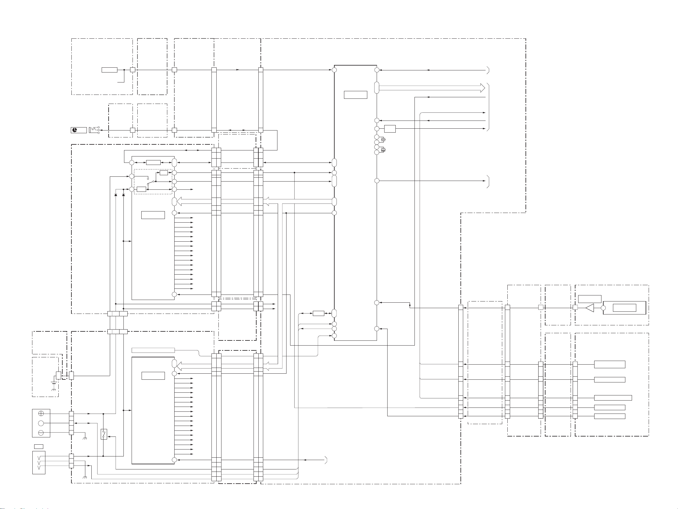
3-2. OVERALL BLOCK DIAGRAM (2/5)
Ver 1.1 2005. 05
( ) : Number in parenthesis ( ) indicates the division number of schematic diagram where the component is located.
VC-367 BOARD(2/5)
TO
OVERALL
BLOCK DIAGRAM
(3/5)
(PAGE 3-5)
TO
OVERALL
BLOCK DIAGRAM
(4/5)
(PAGE 3-8)
TO
OVERALL
BLOCK DIAGRAM
(1/5)
(PAGE 3-1)
TO
OVERALL
BLOCK DIAGRAM
(1/5)
(PAGE 3-1)
16
4
5
2
6
VD SO,SI,SCK
XCS LCD
VSP SO,SCK
BL CONT
PLRE
PLGR
PLBL
XPHD
XPVD
Y
C
CK
EVGR
EVBL
YO
PRO
PBO
ADAO1
AUIN11
CKFSO
CK64FSO
CK256FSO
IC7119
2
VD SO,SI,SCK
FP-088
(FLEXIBLE
BOARD)
CN0008
PLRE
PLGR
3
•
PLBL
2
•
1
11
•
12
•
9
XCS LCD XCS LCD
10
XPHD
14
XPVD
13
15
VA-120 BOARD
(1/4)
3
•
2
10 8
•
1
12 14
12
•
VD SCK,SO,SI
14
•
15
13
PANEL HD
17
PANEL VD
16
BL CONT
18
5 7
IC2204
RGB DRIVE
FFC-093
(FLEXIBLE
BOARD)
CN2008CN2007 CN402CN401
30
•
28
•
26
36
•
40
•
42
38
44
43
45
SW-436 BOARD
(1/3)
30
•
28
•
26
36
•
40
•
42
38
44
43
45
PD-222 BOARD
LCD901
4
5
3
23
COLOR
1
LCD UNIT
6
22
19
•
13
•
12
•
8
•
7
•
2
LED901
BACK
LIGHT
3
1
11
12
10
14
13
15
3
•
2
•
1
•
•
9
VD SO,SI,SCK
CN601
PANEL R,G,B
EXTDA
19
20
21
23
25
35
32
15
14
4
2
BL LO
VR,VG,VB
COM
PSIG
VST,VCK,EN,DWN,
WIDE,HST,HCK2,
HCK1,RGT
BL ANODE
BL CATHODE
CN603
CN604
40
39
38
IC601
RGB DRIVE
48
•
47
•
46
TIMING
GENERATOR
45
43
42
31 28
BL ON
BACK LIGHT
DRIVE
Q601-604
20
•
21
•
22
SCK
14
11
•
12
13
9
10
8
FP-971
FLEXIBLE
BOARD
VD SO,SCK
1
1
2
2
1
1
2
2
VD SO,SCK
CN0002 CN710CN711 CN2005
JU-001 BOARDFP-095
FLEXIBLE
BOARD(1/2)
4
10
28
1
7
25
CN2001 CN801
12
7
9
CN2000
13
16
19
22
CN2001
SY IN
SC IN
VIDEO IN
SY OUT
SC OUT
VIDEO OUT
FP-096 FLEXIBLE
BOARD
Y
PR
PB
AU IN L
AU OUT L
AU IN R
AU OUT R
FP-095
27
21
1
30
24
4
1
6
4
17
14
11
8
CN801(2/2)
(1/2)
FLEXIBLE
BOARD(2/2)
HP-139 BOARD
HP R
4
HP L
1
CN2002 CN701
4
1
CN901
HP R
HP L
18
18
17
17
16
16
303430
34
LNO Y
23
23
LNO PR
26
26
LNO PB
27
27
XLR LINE1
82
82
(10/16)
CH1
(10/16)
AUDIO
A/D CONV.
D/A CONV.
26
27
5
3
VSP SO,SCK
CH2
CH1
CH2
4
13
14
11
12
15
IC7115
6
2
41
39
29
30
(10/16)
IC7113
LINE OUT
GAINUP
(10/16)
IC7114
AUDIO INPUT
SELECT
L OUT
R OUT
VSP SO,SCK
(10/16)
13
3
A AV OUT L
A AV OUT R
A LINE L
A LINE R
EXT MIC L
EXT MIC R
B4
A5
E5
E1
(10/16)
IC7120
SPEAKER AMP
HEADPHONE AMP
HP CH1
D6
HP CH2
B6
SP+
B2
SP-
D2
7
1
6
11
3
8
IC7501
SELECTOR
CH 1
B4
CH 2
A5
83
97
98
75 75
73
83
97
98
73
XLR LINE2
AUDIO OUT L
AUDIO OUT R
HP CH2
HP CH1
18
16
23
26
27
97
98
73
17
303430
828382
Y,OUT
18
C,OUT
17
CK
16
34
23
26
27
83
97
98
7575
73
EVGR
EVBL
YO
PRO
PBO
LINE AU L
LINE AU R
IC2203
IC2200
IC2201
(3/4)
12
10
(3/4)
5
10
(3/4)
12 14
10
5
IC2300
10 13
5 2
Q2314,2315
EVR
IN A OUT A
IN B OUT B
14
8
7
14
8
7
(4/4)
34
36
26
44
5
46
7
910
(3/4)
IC2201
VIDEO
IN/OUT
AGC
ACC
Q2309
Q2308
39
48
42
18
14
22
J801
YC
G
G
YC
S VIDEO
IN-OUT
G
G
J801
VIDEO
IN-OUT
JL-001 BOARD(2/3)
J901
COMPONENT OUT
AUDIO CH 1/3
IN-OUT
AUDIO CH 2/4
IN-OUT
J701
(HEADPHONES)
HVR-M10C/M10E/M10J/M10N/M10P/M10U
VIDEO SIGNAL
AUDIO SIGNAL
3-3 3-4
3-3. OVERALL BLOCK DIAGRAM (3/5)
( ) : Number in parenthesis ( ) indicates the division number of schematic diagram where the component is located.
CPC
(FOR ADJUSTMENT)
VC-367 BOARD (3/5)
TO
OVERALL
3
BLOCK DIAGRAM
(1/5)
(PAGE 3-2)
TO
OVERALL
4
BLOCK DIAGRAM
(2/5)
(PAGE 3-3)
TO
OVERALL
1
BLOCK DIAGRAM
(1/5)
(PAGE 3-1)
TO
OVERALL
7
BLOCK DIAGRAM
(5/5)
(PAGE 3-10)
TO
OVERALL
8
BLOCK DIAGRAM
(4/5)
(PAGE 3-8)
DA-033 BOARD
(2/3)
RF MON
13
SWP
CN107
16
REC CK
REC DT
RF IN
SWP
MC BUS
VCK
SWP,FRRV,TRRT,TRRV
VSP2 SO,SI,SCK
VSP SO,SI,SCK
VD SO,SCK
VSP SO,SCK
XCS_LCD
VD SO,SI,SCK
VD SO,SI,SCK
NTSC/XPAL DET
(14/16)
IC8802
EEPROM
REC LEVEL VOL CH1
REC LEVEL VOL CH2
MANUAL REC CH1
MANUAL REC CH2
HI SO,SI,SCK
REC PROOF
CHIME SDA,CHIME SCK,CHIME VDD
XCC DOWN
5
•
2
EEP SO,SI,SCK
•
6
FP-976 (1)
(FLEXIBLE
BOARD)(3/4)
CN101 CN0003
535353
5315
CN761
CN103
CN760CN761
535353
53
CN0005
CN760
FP-976 (2)
(FLEXIBLE
BOARD)(2/4)
X8801
20MHz
FRRV
TRRT
TRRV
117
178
179
111
113
114
52
|
45
33
|
30
•
•
69
•
70
•
67
82
•
83
•
80
73
•
74
•
71
38
1
3
86
•
87
•
84
•
•
56
•
57
63
•
65
•
68
IC8801
XCS_LCD
NTSC/XPAL
(14/16)
MECHA
CONTROL
CONT1
172
SWP
164
CAP FG
190
CAP ON,CAP FWD
165
•
166
CAP PWM
89
DRUM PWM
88
DRUM FG
197
DRUM PG
198
LOAD,UNLOAD
15
•
13
T REEL FG
192
S REEL FG
193
TAPE END
196
TAPE TOP
195
DEW DET
119
TAPE LED ON
180
106
MODE SW A-MODE SW C
|
108
VSP SO,SCK
DB-018 BOARD (1/2)
H6
(2/2)
G11
IC201
(1/2)
PWM
DRIVE
J6
G8
Q218
SWITCHING
Q219
SWITCHING
CAP ERROR
DRUM ERROR
CN0007
CN0007
CN206
48
51
40
38
44
43
13
17
•
15
3
1
•
2
14
|
12
11
•
10
15
16
19
21
24
23
9
•
10
7
6
5
4
36
26
34
|
32
31
30
|
28
27
FP-230
(FLEXIBLE
BOARD)(1/2)
FP-098
(FLEXIBLE
BOARD)
FP-230
(FLEXIBLE
BOARD)(2/2)
MR-048 BOARD
CN102
REC CK
5
2
13
15
9
10
CN103
18
14
•
16
28
30
•
29
CN0101
15
|
17
18
DRUM VS
•
19
14
13
CN103
12
10
7
8
22
•
21
24
25
26
27
CN102
17
CN103
5
CN102
19
|
21
22
CN103
1
|
3
4
44
REC DT
46
RF IN
35
RF MON
30
CONT1
39
SWP
38
VCK
35
38
•
36
CAP FG
4
CAP ON
CAP FWD
80
•
1
75
CAP VS
•
77
64
•
67
43
41
45
44
53
50
32
•
33
29
25
21 20
19 18
(1/2)
IC0101
REC/PB
AMP
(2/2)
IC201
CAPSTAN
FG AMP
CAPSTAN
MOTOR
DRIVE
DRUM
MOTOR
DRIVE
CAP
PWM
LPF
DRUM
PWM
LPF
DRUM
FG
AMP
DRUM
PG
AMP
LOADING
MOTOR
DRIVE
REEL
FG
AMP
TAPE
END
DETECT
TAPE
TOP
DETECT
26•27
22•23
Z MECHA DECK
(MDX-Z311)
CN104
10
•
9
4
•
3
7•8
74
•
76
•
78
63
•
65
•
68
52
49
69
•
72
ODD
EVEN
T REEL +,–
S REEL +,–
6
•
5
9
•
8
FG 1,2
CAP U,V,W
DRUM U,V,W
LM +,–
CN203
CN201
CN202
DEW AD
XCC DOWN
DRUM
M903
22
•
25
20
|
17
•
4
|
1
•
11
|
14
5
|
10
1
2
1
|
4
5
26
•
25
22
•
23
20
11
18
12
13
|
15
17
7
|
9
CAPSTAN FG
CAPSTAN
MOTOR
M
M901
DRUM
MOTOR
M
DRUM FG
DRUM PG
M902
LOADING
MOTOR
M
DEW
SENSOR
H902
T REEL
SENSOR
H901
S REEL
SENSOR
Q901
TAPE END SENSOR
Q902
TAPE TOP SENSOR
D901
TAPE LED
MIC902
REC PROOF
4PIN
CONNECTOR
S903
C. C. DOWN
MODE
SWITCH
S902
HVR-M10C/M10E/M10J/M10N/M10P/M10U
VIDEO/AUDIO SIGNAL
3-5 3-6
3-4. OVERALL BLOCK DIAGRAM (4/5)
PW-129 BOARD(1/2)
S602
POWER ON
VTR ON SW
JL-001
BOARD
J931
LANC
(3/3)
DA-033 BOARD
(3/3)
CN104
8 19,20 11-18
FFC-095
FLEXIBLE
DB-018
BOARD (2/2)
8 19,20 11-18
FLAT CABLE
LI-073
16
BOARD
BT591
LITHIUM
BATTERY
(SECONDARY)
BT901
BATTERY
TERMINAL
S
J901
DC IN
CN501
CN207
1
5
VBATT
•
•
2
6
CN204
1
3
4
CN203
1
2
3
Q307,
Q304
HVR-M10C/M10E/M10J/M10N/M10P/M10U
VBATT
CN901
K2
D2
C1
CN205
5
12
LANC SIG
FFC-094
FLEXIBLE
BOARD
FP-096
FLEXIBLE
BOARD
LANC I/O
3V REG
IC101
DC/DC
CONVERTER
RESET
LANC I/O
NTSC/PAL SELECT SW
(2/2)
IC201
DC/DC
CONVERTER
( ) : Number in parenthesis ( ) indicates the division number of schematic diagram where the component is located.
VA-120
BOARD (3/4)
FP-971
(FLEXIBLE
VC-367 BOARD (4/5)
BOARD)(2/2)
LANC SIG
RESET
CN2005
CN2003
XVTR ON SW
4
CN2000
LANC SIG
1
LANC OUT
LANC IN
L3
•
K3
HI XRESET
A3
VOUT
D3
C2
E2
•
E3
D1
G1
EVER 3.0V
FR EVER SO,SCK FR EVER SO,SCK
VTR DD ON
A 1.5V
CAM 1.5V
D1 1.5V
D 1.2V
D 1.9V
A 4.6V
AU 4.6V
D 3.1V
D1 2.8V
A1 2.8V
CAM 5.1V
RP 4.6V
CAM -7.5V
EP 13.5V
A -2.8V
CAM 15V
CAM DD ON
BATT UNREG
VTR UNREG
CN710 CN0002
63
47
FP-976 (2)
11
11
5
5
•
•
3
3
39
39
47
47
•
•
49
49
31
31
•
•
29
29
33
33
(FLEXIBLE
BOARD)(3/4)
CN761
CN761
CN103
CN101
FP-976 (1)
(FLEXIBLE
BOARD)
(3/3)
35
35
CN103 CN0005
CN761
50
50
48
48
FP-976 (2)
(FLEXIBLE
BOARD)
(4/4)
CN760
CN760
CN760
CN711
CN0008
SIRCS SIG FRONT
XCC DOWN
TXD,RXD,SCK
CAM DD ON
KEY AD0 VM
KEY AD1 VM
KEY AD2 VM
XEJECT SW
CHARGE LED
NTSC/XPAL DET
30
FP-088
(FLEXIBLE
63
1 5
XVTR ON SW
(12/16)
XCC DOWN
SI
SO
SCK
23
•
24
•
25
IC8301
FRONT
CONTROL
XEJECT SW
4
Q8308
LED
SIRCS SIG
X TAL
X TAL
9
DRIVE
X 0A
52
X8302
32.768KHz
51
X 1A
29
X8301
10MHz
28
46
41
47
CN0005
11
11
5
5
•
•
3
3
CN0003
39
39
47
47
•
•
49
49
31
31
•
•
29
29
33
33
35
35
504850
48
BATT SIG
40
•
39
73
14
•
53
•
62
20
•
21
35
Q8307
42
I/F
•
43
77
37 6
75
LANC OUT
LANC IN
XRESET
VCC
HI EVER SO
HI EVER SCK
VTR DD ON
IB SO
IB SI
BATT/XEXT
FAST CHARGE
INIT NTSC/XPAL
XCHARGE LED
NTSC/PAL OUT
XBATT INFO SW
BOARD)
CN201 CN0001
CN771
80 80
6
E2
•
E3
FR EVER SO,SCK
VTR DD ON
D1
(2/2)
L9
BL CONT
D2 1.5V
D 1.0V
CAM 2.5V
D 2.5V
CAM 3.6V
CAM 2.8V
EP 2.8V
RP 2.8V
D2 2.8V
A2 2.8V
AU 4.9V
EVF 4.9V
MT 4.9V
AU 8V
RP 13.5V
BL HIV
BL LO
FAST CHARGE
BATT SIG
BATT/XEXT
6
•
•
4
4
8
8
20
20
14
14
12
12
22
22
FP-977
(FLEXIBLE
BOARD)
CN770
80 80
6
•
4
8
20
14
12
22
(2/2)
6
•
4
8
20
14
12
22
BL CONT
TO
OVERALL
BLOCK DIAGRAM
(2/5)
(PAGE 3-3)
5
KEY AD0 VM
KEY AD1 VM
KEY AD2 VM
HI RESET
XBATT INFO SW
27
26
25
24
23
3-7 3-8
TO
OVERALL
BLOCK DIAGRAM
(3/5)
(PAGE 3-5)
TO
OVERALL
BLOCK DIAGRAM
(5/5)
(PAGE 3-9)
TO
OVERALL
BLOCK DIAGRAM
(1/5)
(PAGE 3-1)
8
9
q;
37
33
32
31
30
29
VA-120
BOARD
(2/4)
KEY AD0 VM
KEY AD1 VM
KEY AD2 VM
HI XRESET
XBATT INFO SW
7
9
8
7
16
4
CN2008CN2007 CN401
FFC-094
FLEXIBLE
BOARD
FFC-093
FLEXIBLE
BOARD
KEY AD0 VM
KEY AD1 VM
KEY AD2 VM
XRESET
BATT INFO
Ver 1.1 2005. 05
PW-129 BOARD (2/2)
IC601
2
CN601CN2003
SW-436 BOARD(2/3)
9
8
7
16
4
41.2
S001-S005
STOP,PB,REW,FF
S011-013
LCD BRIGHT +/-,PAUSE
S021-S024
REC,INDEX,AUDIO DUB,TC/U-BIT
S111
S112
DISPLAY/BATT INFO
1
LCD ON/OFF
RESET
IC602
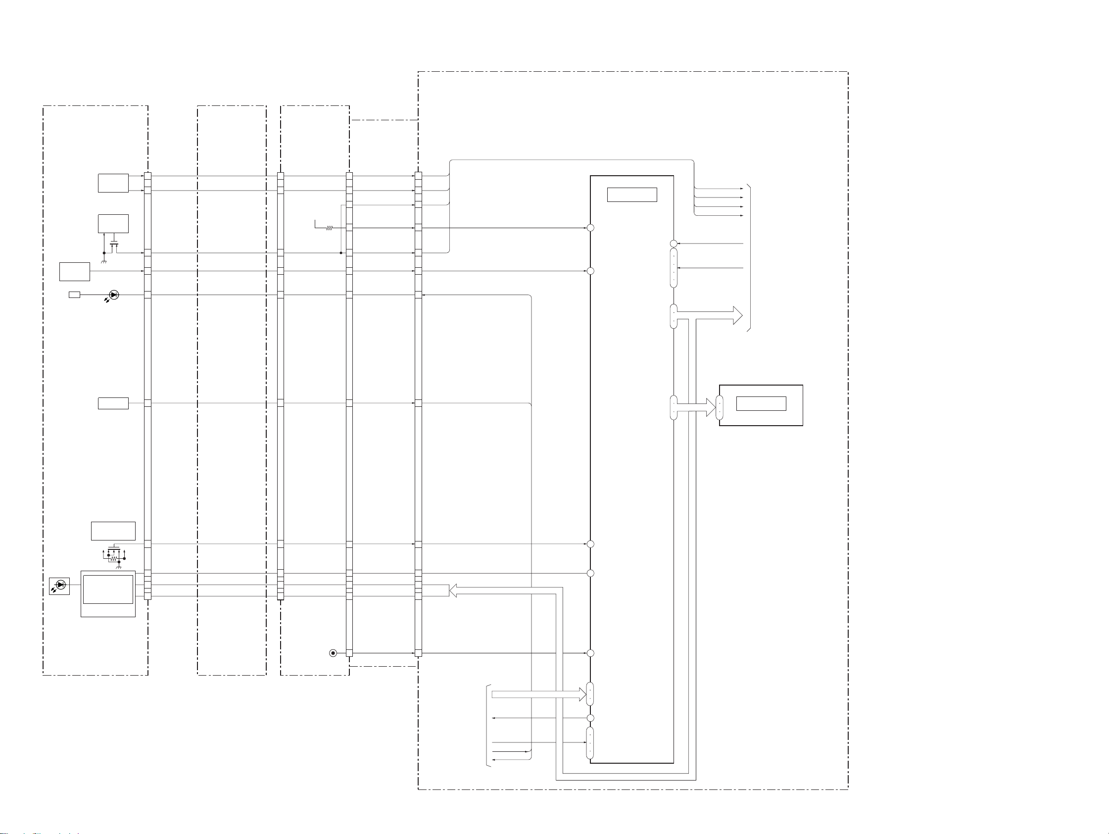
3-5. OVERALL BLOCK DIAGRAM (5/5)
Ver 1.1 2005. 05
( ) : Number in parenthesis ( ) indicates the division number of schematic diagram where the component is located.
VC-367 BOARD (5/5)
SW-436
BOARD(3/3)
S041-S045
EXEL,MENU
MENU+MENU-
STATUS
D110
CHG
RV001,002
AUDIO REC
LEVEL
S110
AUDIO LEVEL
MANUAL/AUTO
S113
DOOR OPEN
FFC-093
FLEXIBLE
BOARD
VA-120(4/4)
BOARD
FP-089
(FLEXBLE
BOARD)
CN2006CN2008CN401
11
12
14
6
23
2
11
12
D2 2.8V
14
6
23
2
REC LEVEL VOL CH1 CN0004
2
REC LEVEL VOL CH2
4
MANUAL REC CH2
8
KEY AD7 VM
24 20
MANUAL REC CH1
7
KEY AD4 VM
21
CHARGE LED
39
XEJECT SW
11
2
4
7
137
6
17
33
9
143
KEY AD7 VM
KEY AD4 VM
(11/16)
IC8009
HI CONTROL (2/2)
REC PROOF
CHIME SDA
CHIME SCK
CHIME AD0
CHIME AD1
CHIME AD2
HI SO
HI SI
XHI SCK
EEP TXD
EEP RXD
EEP SCK
REC LEVEL VOL CH1
REC LEVEL VOL CH2
MANUAL REC CH1
MANUAL REC CH2
HI SO, SI, SCK
HI SO, SI, SCK
REC PROOF
CHIME SDA
CHIME SCK
CHIME VDD
5
2
6
7
(11/16)
IC8002
EEPROM
TO OVERALL
BLOCK DIAGRAM (3/5)
(PAGE 3-5)
234
246
247
134
135
136
97
98
99
103
104
105
S061
INPUT SELECT
VIDEO-S VIDEO-HDV/DV
D001-D013
IC003
IC004
LED DRIVE
22
20
18
HVR-M10C/M10E/M10J/M10N/M10P/M10U
KEY AD6 VM
CL2001
23
30
29
28
22
XCS CAM COM
XHI SCK
HI SO
KEY AD5 VM
55
22
20
18
19
25
24
23
18
TO
OVER ALL
9
BLOCK DIAGRAM
(4/5)
(PAGE 3-8)
HI SO, SCK
CAM DO ON
KEY ADO VM
KEY AD1 VM
KEY AD2 VM
KEY AD3 VM
XCHARGE LED
XEJECT SW
TXD, RXD, SCK
145
269
144
93
94
95
131
139
140
141
142
KEY AD6 VM
XCS FKAMERA
KEY AD5 VM
TXD
RXD
SCK
CAM DD ON
KEY AD0 VM
KEY AD1 VM
KEY AD2 VM
KEY AD3 VM
3-9 3-10
 Loading...