

Page 1
HCD-VB5
Main Unit
Amplifier section
The following measured at 220 V AC, 50/60 Hz
DIN power output (rated): 10 + 10 watts
(4 ohms at 1 kHz, DIN)
Continuous RMS power output (reference):
12 + 12 watts
(4 ohms at 1 kHz, 10% THD)
The following measured at 240 V AC, 50/60 Hz
DIN power output (rated): 12 + 12 watts
(4 ohms at 1 kHz, DIN)
Continuous RMS power output (reference):
15 + 15 watts
(4 ohms at 1 kHz, 10% THD)
Inputs
MD/VIDEO (AUDIO) IN (phono jacks):
voltage 500/250 mV, impedance
47 kilohms
MIC (mini jack): Sensitivity 1 mV, impedance
10 kilohms
Outputs
MD/VIDEO (AUDIO) OUT (phono jack):
voltage 250 mV, impedance
1 kilohm
VIDEO OUT (phono jack):
max. output level 1 Vp-p,
unbalanced, Sync negative, load
impedance 75 ohms
S VIDEO OUT (4-pin/mini-DIN jack):
Y: 1 Vp-p, unbalanced, Sync
negative,
C: 0.286 Vp-p, load impedance
75 ohms
PHONES (stereo minijack):
accepts headphones of 8 ohms or
more.
SPEAKER: accepts impedance of 4 to
16 ohms.
CD DIGITAL OUT OPTICAL:
Optical
VIDEO CD/CD player section
System Compact disc and digital audio and
video system
Laser Semiconductor laser (λ = 780 nm)
Emission duration: continuous
Laser output Max. 44.6 mW*
* This output is the value
measured at a distance of
200 mm from the objective lens
surface on the Optical Pick-up
Block with 7 mm aperture.
Wavelength 780 – 790 nm
Frequency response 2 Hz – 20 kHz (±0.5 dB)
Signal-to-noise ratio More than 90 dB
Dynamic range More than 90 dB
Video color system format
NTSC, PAL
CD DIGITAL OUT OPTICAL
(Square optical connector jack, rear panel)
Wavelength 666 nm
Output Level –18 dBm
Tuner section
FM stereo, FM/AM superheterodyne tuner
FM tuner section
Tuning range 87.5 – 108.0 MHz
(50 kHz step)
Antenna FM lead antenna
Antenna terminals 75 ohms unbalanced
Intermediate frequency 10.7 MHz
AM tuner section
Tuning range 531 – 1,602 kHz
(with the interval set at 9 kHz)
530 – 1,710 kHz
(with the interval set at 10 kHz)
Antenna AM loop antenna
External antenna terminals
Intermediate frequency 450 kHz
General
Power requirements 110 – 120 V or 220 – 240 V AC,
50/60 Hz
Adjustable with voltage selector
Power consumption 50 watts
Dimensions (w/h/d) Approx. 180 × 130 × 315 mm
incl. projecting parts and controls
Mass Approx. 4.0 kg
Supplied accessories Remote (1)
Size AA (R6) batteries (2)
AM loop antenna (1)
FM lead antenna (1)
Speaker cords (2)
Video cord (1)
Design and specifications are subject to change
without notice.
SERVICE MANUAL
• This set is the Amplifier and VIDEO CD/
CD player section in CMT-VB5.
SPECIFICATIONS
E Model
Model Name Using Similar Mechanism NEW
CD Mechanism Type CDM55C-K6BD37A
Base Unit Name BU-K6BD37A
Optical Pick-up Name KSM-213DCP/Z-NP
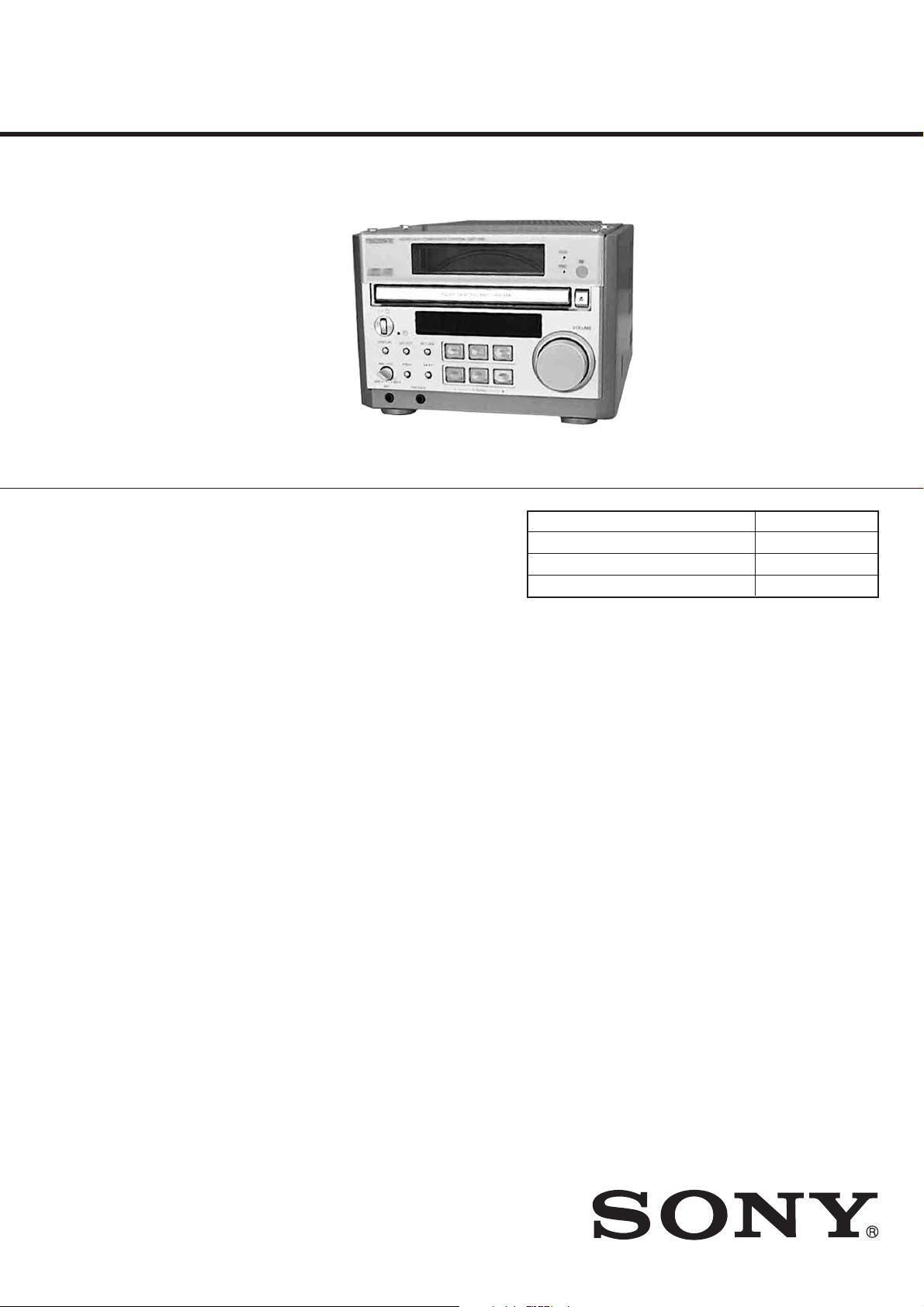
MICRO Hi-Fi COMPONENT SYSTEM
Page 2
TABLE OF CONTENTS
1. GENERAL ·········································································· 3
2. DISASSEMBLY ································································ 5
3. SERVICE MODE······························································8
4. ELECTRICAL ADJUSTMENTS ································· 9
5. DIAGRAMS
5-1. BLOCK DIAGRAM –CD SECTION– ······················· 11
–VIDEO SECTION–··················································· 12
–MAIN SECTION– ···················································· 13
–PANEL/POWER SECTION–···································· 14
5-2. Circuit Boards Location ·············································· 15
5-3. Wa veforms ···································································15
5-4. PRINTED WIRING BOARD –BD SECTION–·······16
5-5. SCHEMATIC DIAGRAM –BD SECTION–············ 17
5-6. PRINTED WIRING BOARDS
–MAIN SECTION– ··················································· 18
5-7. SCHEMATIC DIAGRAM
–MAIN SECTION(1/2)– ··········································· 19
5-8. SCHEMATIC DIAGRAM
–MAIN SECTION(2/2)– ··········································· 20
5-9. PRINTED WIRING BOARDS
–POWER SECTION– ················································ 21
5-10. PRINTED WIRING BOARD
–PANEL SECTION– ················································· 22
5-11. SCHEMATIC DIAGRAM
–PANEL SECTION– ················································· 23
5-12. PRINTED WIRING BOARDS
–VIDEO CD SECTION– ·········································· 24
5-13. SCHEMATIC DIAGRAM
–VIDEO CD SECTION(1/2)– ··································· 25
5-14. SCHEMATIC DIAGRAM
–VIDEO CD SECTION(2/2)– ··································· 26
5-15. SCHEMATIC DIAGRAM
–LOADING SECTION–············································27
5-16. PRINTED WIRING BOARDS
–LOADING SECTION–············································27
5-17. IC Pin Function ·························································· 28
5-18. IC Block Diagrams·····················································32
6. EXPLODED VIEWS ................................................... 34
7. ELECTRICAL PARTS LIST ................................... 39
NOTES ON HANDLING THE OPTICAL PICK-UP
BLOCK OR BASE UNIT
The laser diode in the optical pick-up block may suffer electrostatic
break-down because of the potential difference generated by the
charged electrostatic load, etc. on clothing and the human body.
During repair, pay attention to electrostatic break-down and also
use the procedure in the printed matter which is included in the
repair parts.
The flexible board is easily damaged and should be handled with
care.
NOTES ON LASER DIODE EMISSION CHECK
The laser beam on this model is concentrated so as to be focused on
the disc reflective surface by the objective lens in the optical pickup block. Therefore, when checking the laser diode emission,
observe from more than 30 cm away from the objective lens.
Notes on chip component replacement
• Never reuse a disconnected chip component.
• Notice that the minus side of a tantalum capacitor may be damaged by heat.
Flexible Circuit Board Repairing
• Keep the temperature of the soldering iron around 270 ˚C during repairing.
• Do not touch the soldering iron on the same conductor of the
circuit board (within 3 times).
• Be careful not to apply force on the conductor when soldering
or unsoldering.
CAUTION
Use of controls or adjustments or performance of procedures
other than those specified herein may result in hazardous
radiation exposure.
This appliance is classified as a CLASS 1 LASER product.
The CLASS 1 LASER PRODUCT MARKING is located on
the rear exterior.
SAFETY-RELATED COMPONENT WARNING!!
COMPONENTS IDENTIFIED BY MARK 0 OR DOTTED LINE WITH
MARK 0 ON THE SCHEMATIC DIAGRAMS AND IN THE PARTS
LIST ARE CRITICAL TO SAFE OPERATION. REPLACE THESE
COMPONENTS WITH SONY PARTS WHOSE PART NUMBERS
APPEAR AS SHOWN IN THIS MANUAL OR IN SUPPLEMENTS
PUBLISHED BY SONY .
2
Laser component in this product is capable of emitting radiation
exceeding the limit for Class 1.
Page 3
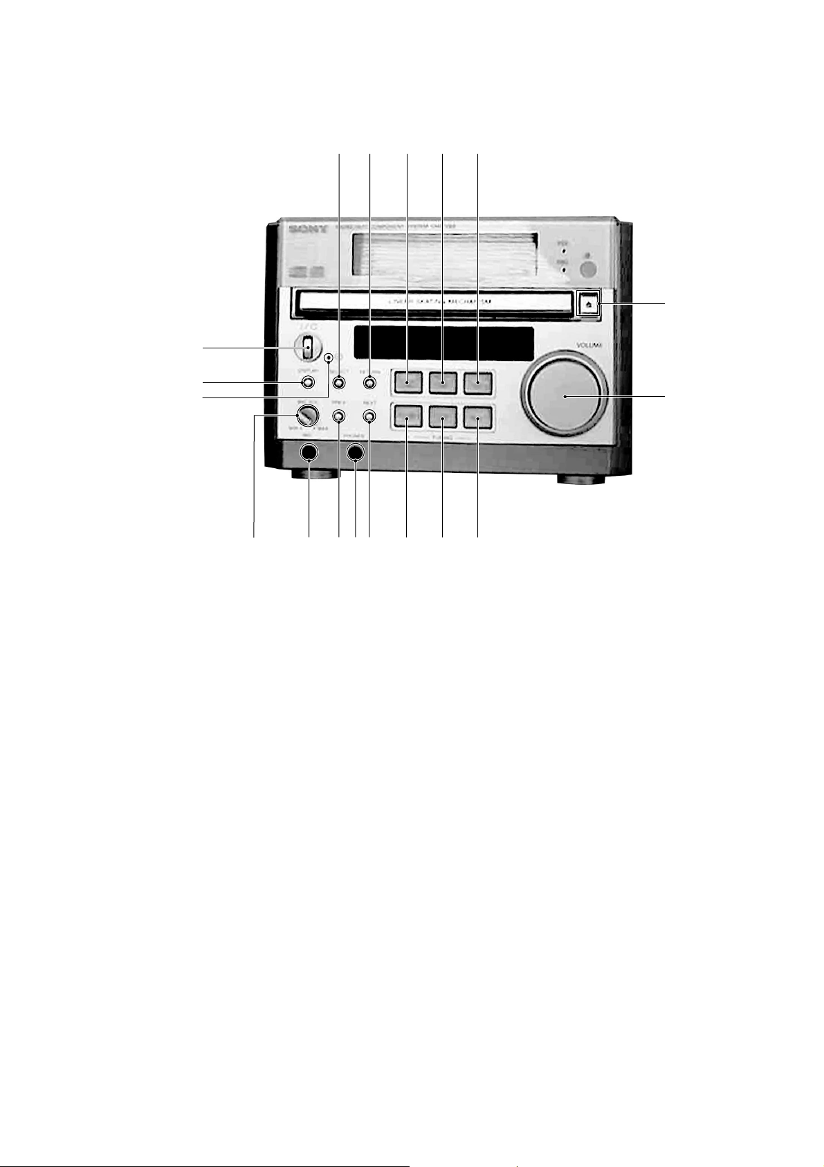
LOCATION OF CONTROLS
– Front Panel –
1
2
3
SECTION 1
GENERAL
654
9
q;
qh qf
qjqk qg
1 ?/1 button
2 DISPLAY button
3 t indicator
4 SELECT button
5 RETURN button
6 TUNER/BAND button
7 7 button
8 FUNCTION button
9 Z button
q; VOLUME knob
qd7qs8qa
qa J L button
qs s button
qd l j button
qf NEXT button
qg PHONES jack
qh PREV button
qj MIC jack
qk MIC VOL knob
3
Page 4
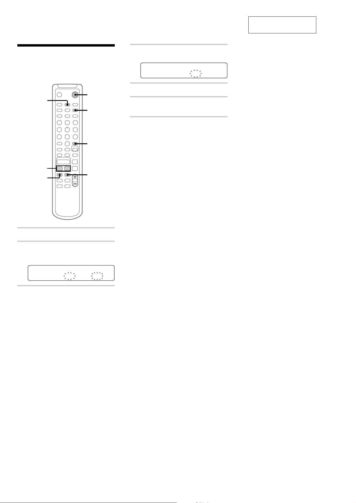
Step 2: Setting the time
You must set the time beforehand to use the timer
functions.
`/1
1
DISPLAY
2
4,6
O
X
H
>
x
3,5
m
1
Turn on the system.
.
Mm
4
4
Press ENTER or M.
The minute indication flashes.
11:00 AM
5
Press ./> to set the minute.
6
Press ENTER.
The clock starts.
If you made a mistake
Press m/M repeatedly until the incorrect item
flashes, then set it again.
To change the preset time
You can change the preset time while the system
is off.
1 Press DISPLAY to display the clock.
2 Press CLOCK/TIMER SET.
3 Repeat steps 3 to 6 of “Setting the time.”
Tips
• The upper dot of the colon flashes for the first 30
seconds, and the lower dot flashes for the last 30
seconds of each minute.
• Each time you press DISPLAY while the system is
off, the display switches between no display and the
clock display.
This section is extracted
from instruction manual.
2
Press CLOCK/TIMER SET.
The clock appears and the hour indication
flashes.
21 :00 AM
3
Press ./> to set the hour.
4
Page 5
SECTION 2
9
ten screws
(BVTP3
×
10)
q;
one screw
(BVTP3
×
10)
8
case (left)
2
plate top
5
case (right)
qs
back panel
qa
case (top)
6
two case screws
1
four screws
3
two case screws
4
one screw
(BVTP3
×
10)
7
one screw
(BVTP3
×
10)
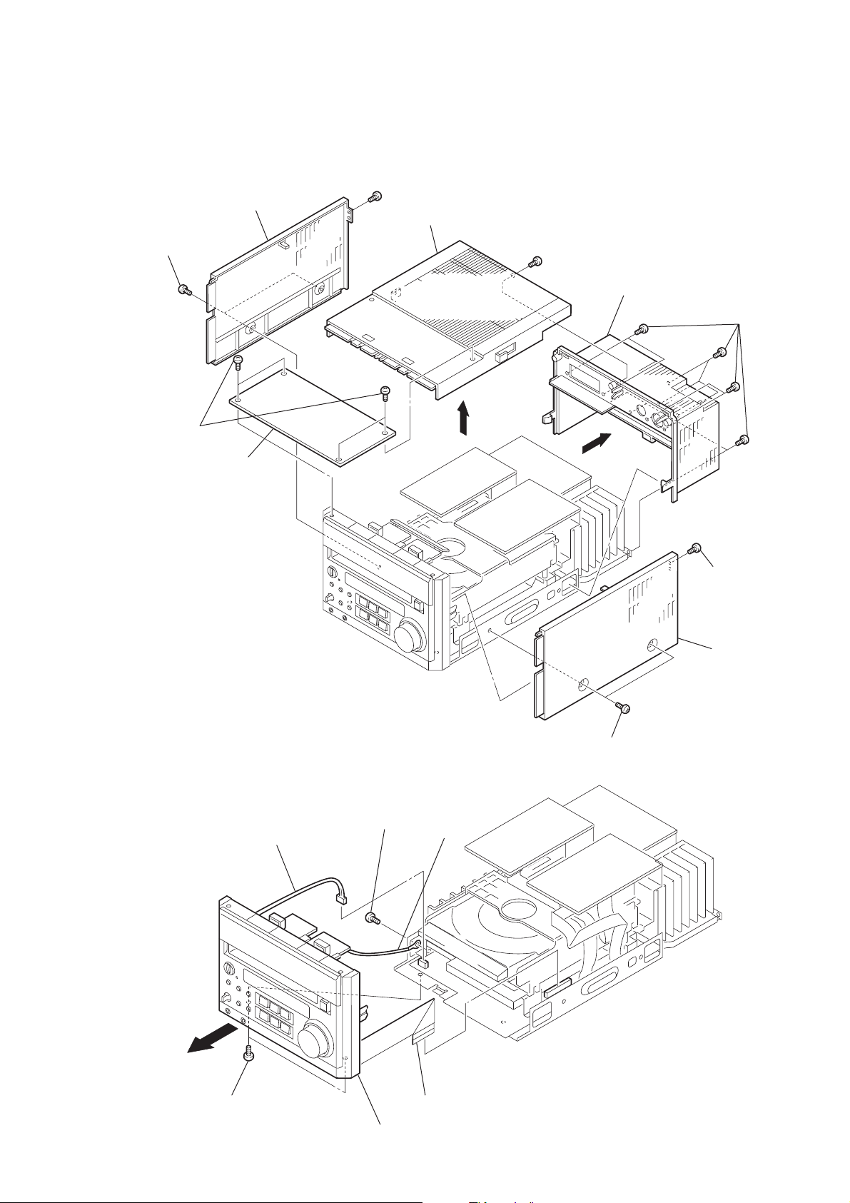
DISASSEMBLY
Note: Follow the disassembly procedure in the numerical order given.
2-1. CASE (TOP)
2-2. FRONT PANEL ASSY
2
connector
(CN202)
3
one screw
(BVTP3
×
8)
4
lug
5
two screws
(BVTP3
1
wire (flat type)(23 core)
×
8)
6
front panel assy
(CN441)
5
Page 6
2-3. CD MECHANISM DECK (CDM55C-K6BD37A)
4
CD mechanism deck
(CDM55C-K6BD37A)
3
screw
(BVTP3 × 8)
1
wire (flat type)
(23 core)(CN501)
2
2-4. BASE UNIT (BU-K6BD37A)
2
base unit
(BU-K6BD37A)
connector
(CN1)
1
floating screw
(PTPWHM2.6)
6
Page 7
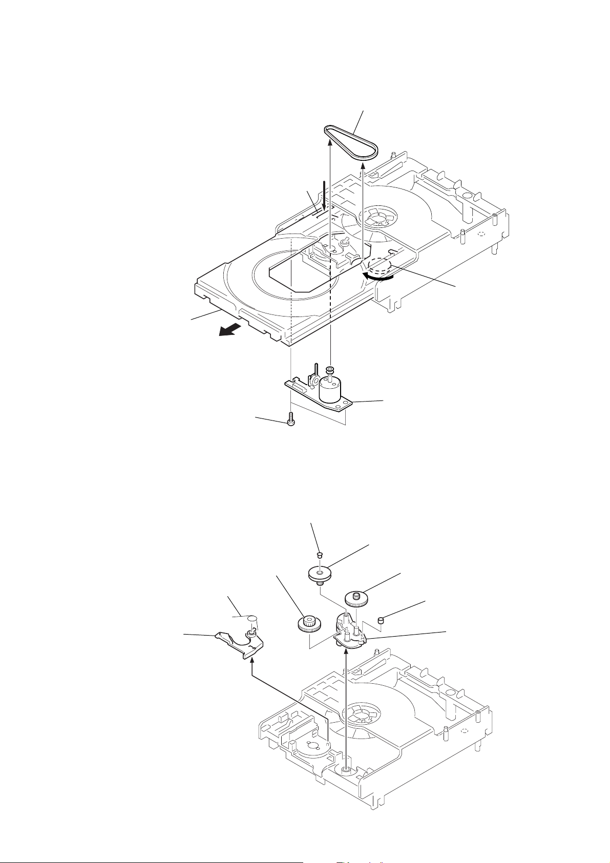
2-5. LOADING BOARD
2
belt (CDM55)
B
3
Pull the tray pushing B.
4
two screws
(BTP2.6
×
6)
5
LOADING board
1
Rotate the gear(B) in
the direction of arrow
A
.
A
)
2-6. CAM (CDM55C-K6BD37A)
1
torsion spring
2
lever (SW)
6
gear (B)
3
spacer (55)
4
pulley (LDG)
5
gear (A)
7
roller
8
cam (CDM55
7
Page 8

SECTION 3
SERVICE MODE
[Panel T est Mode]
Procedure:
1. Set to standby state.
2. Press three buttons of s , ?/1 , and 7 simultaneously.
3. Liquid crystal display and LED are all turned on.
4. Pless Z to enter the version display mode.
5. Press 7 to enter the KEY, VOL, check mode. ( l j
and J L must be pressed for several seconds.)
6. To exit from this mode, press the buttons in the same way as
step 2.
[Cold Reset]
Clears all the memories and starts up the machine again.
Procedure:
1. Set to standby state.
2. Press three b uttons of s , ?/1 , and FUNCTION simultaneously.
[Hot Reset]
Starts up the machine again holding the memory data.
Procedure:
1. Set to standby state.
2. Press three buttons of s , ?/1 , and 7 simultaneously.
8
Page 9
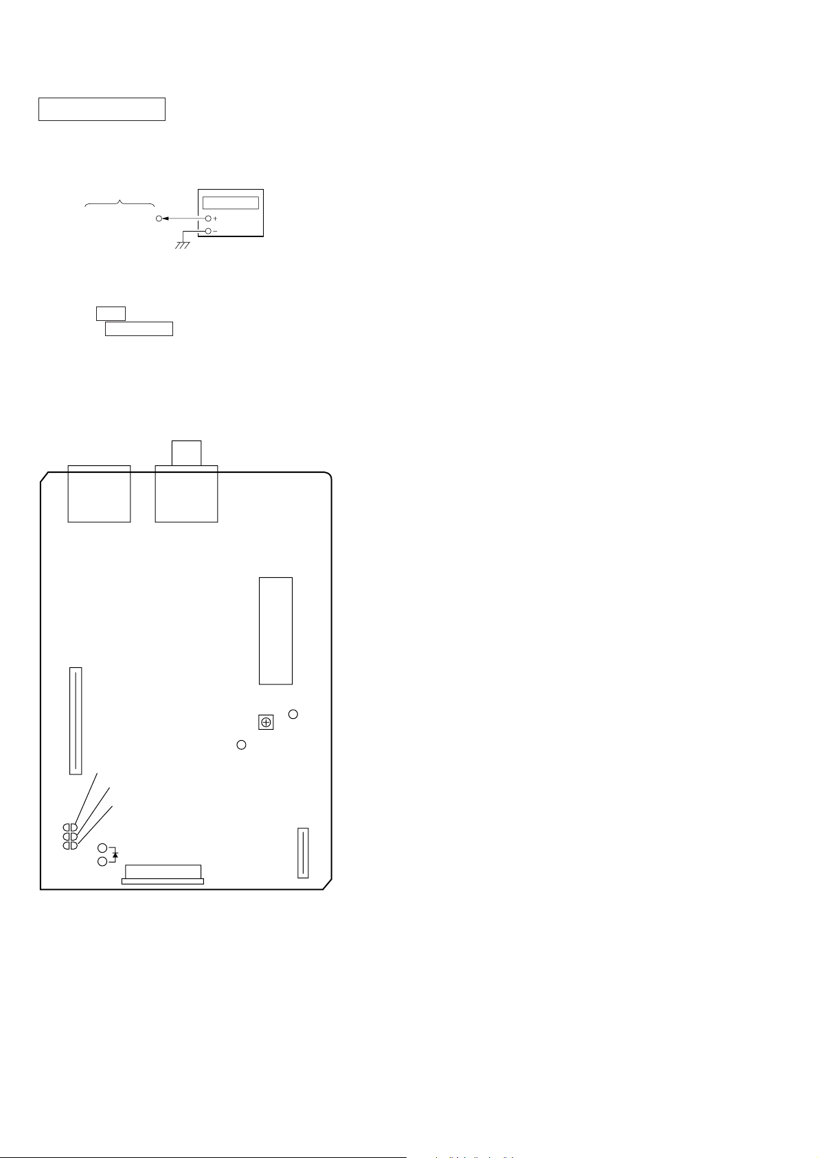
e
TP(TEO)
TP(VC)
BD board
Oscilloscope
Level=1.3 ±0.6 Vp-p
Symmetry
A (DC voltage)
Center of
waveform
B
0 V
1 track jump waveform
Specified level: × 100 = less than ± 22 %
B
A
SECTION 4
ELECTRICAL ADJUSTMENTS
CD SECTION
Note :
1. CD Block is basically designed to operate without adjustment.
Therefore, check each item in order given.
2. Use YEDS-18 disc (3-702-101-01) unless otherwise indicated.
3. Use an oscilloscope with more than 10MΩ impedance.
4. Clean the object lens by an applicator with neutral detergent
when the signal level is low than specified value with the
following checks.
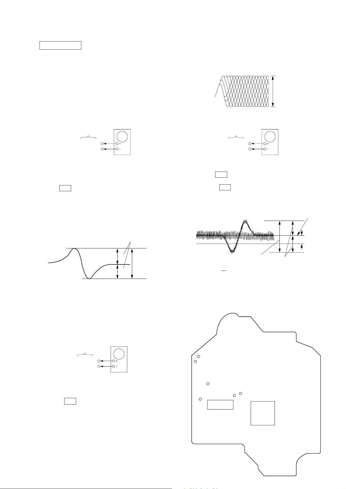
S-Curve Check
Oscilloscope
BD board
TP(FEO)
TP(VC)
Procedure :
1. Connect oscilloscope to TP (FEO).
2. Connect between TP (FEI) and TP (VC) by lead wire.
3. Connect between TP (AGCCON) and TP (GND) by lead wire.
4. Turn ?/1 button on.
5. Load a disc (YEDS-18) and actuate the focus search. (In
consequence of open and close the disc tray, actuate the focus
search)
6. Confirm that the oscilloscope waveform (S-curve) is
symmetrical between A and B. And confirm peak to peak level
within 4 ±1 Vp-p.
S-curve waveform
Symmetry
Note : Clear RF signal waveform means that the shape “ ◊ ” can be
clearly distinguished at the center of the waveform.
RF signal waveform
VOLT/DIV : 200mV
TIME/DIV : 500ns
±
Level : 1.45
0.3Vp-p
E-F Balance (1 Track jump) Check
Procedure :
1. Connect oscilloscope to TP (TEO) and TP (VC).
2. Turned ?/1 button on.
3. Load a disc (YEDS-18) and playback the number five track.
4. Press the 7 button. (Becomes the 1 track jump mode.)
5. Confirm that the level B and A (DC voltage) on the oscilloscope
waveform.
7. After check, remove the lead wire connected in step 2 and 3.
Note : • Try to measure several times to make sure than the ratio
RF Level Check
Procedure :
1. Connect oscilloscope to TP (RF).
2. Connect between TP (AGCCON) and TP (GND) by lead wire.
3. Turned ?/1 button on.
4. Load a disc (YEDS-18) and playback.
5. Confirm that oscilloscope wavefor m is clear and check RF signal
6. After check, remove the lead wire connected in step 2.
A
Wthin 4
B
of A : B or B : A is more than 10 : 7.
• Take sweep time as long as possible and light up the
brightness to obtain best waveform.
Oscilloscop
BD board
TP(RF)
TP(VC)
level is correct or not.
±
1Vp-p
6. After check, remove the lead wire connected in step 1.
Adjustment Location:
[BD BOARD] (Conductor Side)
TP (RF)
TP (VC)
TP (AGCCON)
TP (TEO)
IC101
TP
(GND)
TP (FE0)
IC103
9
Page 10
VIDEO SECTION
r
Frequency Adjustment
Connection:
VIDEO board
(27 MHz)
frequency counte
Procedure:
1. Connect the frequency counter to check point of the VIDEO
board.
2. Turned ?/1 button switch on.
3. Press the FUNCTION button to select the CD.
4. Adjust CT503 on the VIDEO board so that the frequency counter
reading 27.0 MHz ± 80 Hz at stop status.
Adjustment Location:
[VIDEO BOARD] (SIDE A)
J301
J302
IC507
CN501
SL503
SL502
SL501
CHECK LED
CN502
(27MHz)
(GND)
CT503
VIDEO
Frequency
Adjustment
CN503
10
Page 11
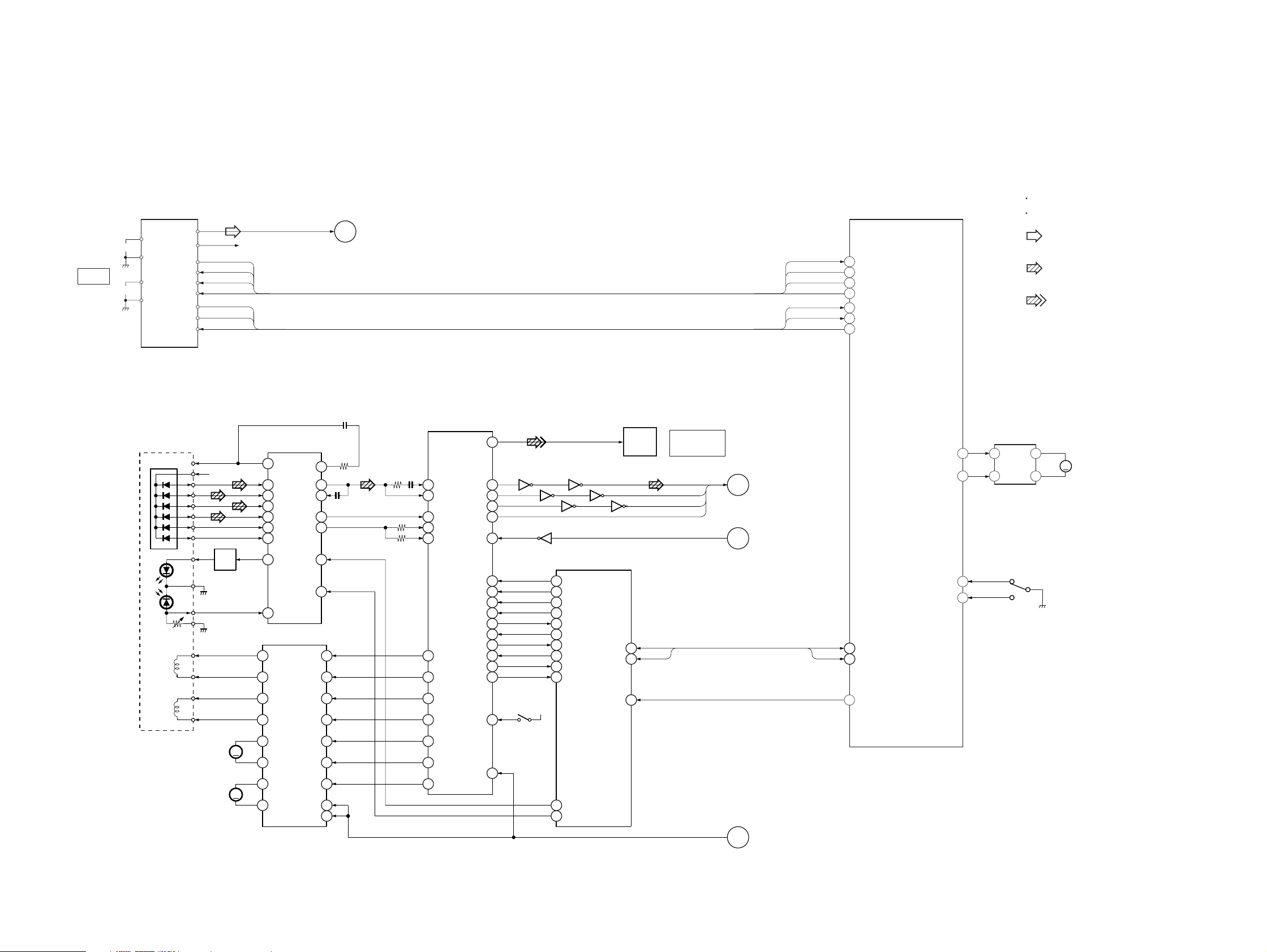
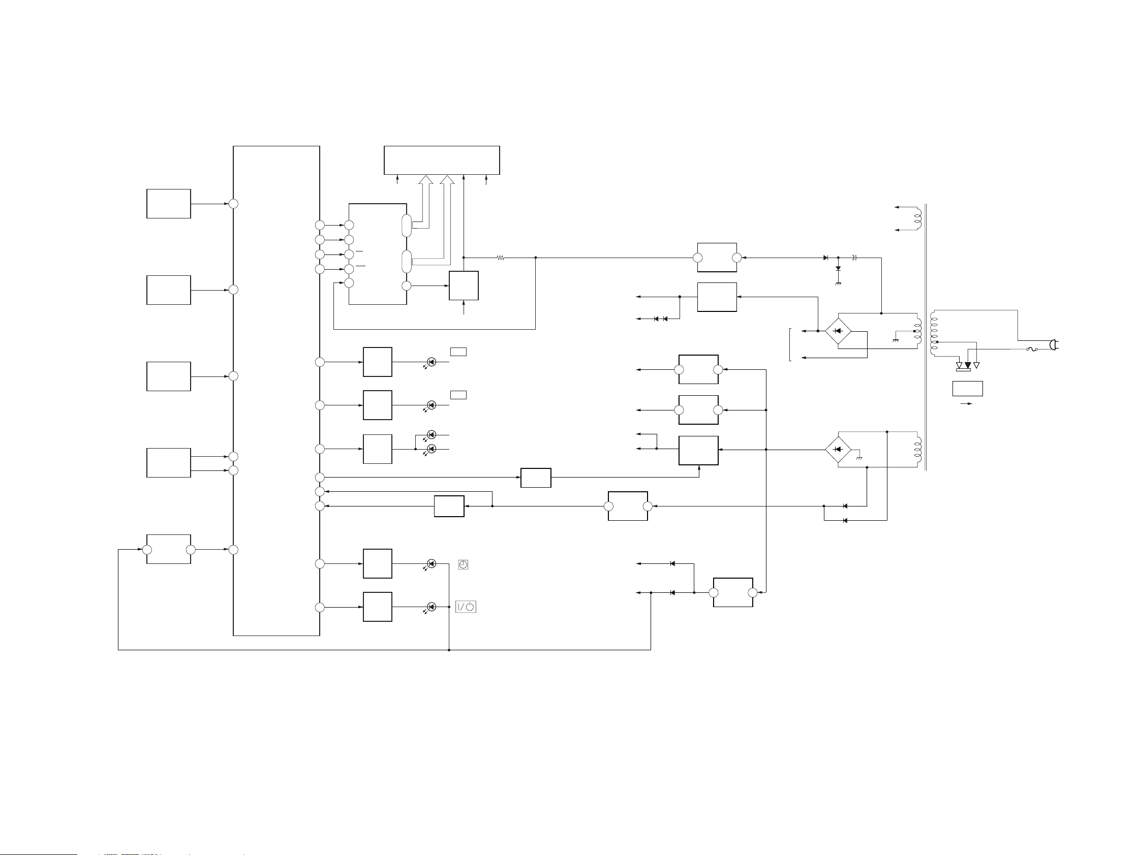
5-1. BLOCK DIAGRAM – CD SECTION –
SECTION 5
HCD-VB5
DIAGRAMS
ANTENNA
TUNER UNIT
ST-L
BLOCK
VR
COIL
COIL
ST-R
ST DOUT
ST DIN
ST CLK
ST CE
TUNED
STEREO
MUTE
VC
A
B
C
D
E
F
LD
GND
PD
F+
F-
T+
T-
FM
AM
OPTICAL PICK-UP
(KSM-213DCP/Z-NP)
FOCUS
TRACKING
16
+5V
DRIVE
M102
SLED
MOTOR
M101
SPINDLE
MOTOR
STDI
STDO
STCK
STCE
TUNED
STEREO
STMT
Q101
LD
IC601 (1/3)
SYSTEM CONTROLLER
54
ST_DIN
53
ST_DOUT
55
ST_CLK
52
ST_CE
51
TUNED
50
STEREO
ST_MUTE
49
IIC_DATA
30
29
59
XRST
LOAD_OUT
LOAD_IN
IN_SW
OPEN_SW
MOTOR DRIVER
5
66
6
67
70
71
TUNER-L
R-CH
IC103
RF AMP
12
VC
5
A
6
B
7
C
8
D
11
E
10
F
3
LD
4
PD
MOTOR/COIL DRIVE
14
VO1(+)
13
VO1(-)
12
VO2(+)
11
VO2(-)
15
VO4(+)
RFE
RFO
LD ON
HOLD SW
IC102
OP1(+)
OP1(-)
OP2(+)
OP2(-)
OP4(+)
15
16
RFI
17
14FE
13TE
22
21
2
3
5
6
27
M
16
17
VO4(-)
VO3(+)
OP4(-)
OP3(-)
26
23
A
MAIN
SECTION
(Page 13)
IC101
DIGITAL SERVO
DIGITAL SIGNAL PROC.
D OUT
50
43
39
41
40
33
34
31
32
29
30
25
RFAC
RFDC
FE
TE
SE
FFDR
FRDR
TFDR
TRDR
SFDR
SRDR
MDP
PCMD
BCLK
DATA
CLOK
XLAT
MUTE
SQSO
SQCK
SENS
SCLK
SCOR
XTSL
XRST
STDI
STDO
STCK
STCE
TUNED
STEREO
STMT
IC101
CD
DIGITAL OUT
OPTICAL
CD DATA
CD BCK
CD LRCK
C2PO
MCLK
B
C
I2C-DATA
I2C-CLK
XRST
VIDEO
SECTION
(Page 12)
VIDEO
SECTION
(Page 12)
I2C.DATA
I2C.CLK
XRESET
DIGITAL
OUT
30
29
12
64
IC501
LEVEL SHIFT
66
67
65LRCK
14C2PO
IC104
S101
LIMIT
IN SW
42
95
DSP DATA
5
DSP CLK
97
DSP LATCH
10
DSP MUTE
36
SUBQ DATA
37
SUBQ CLK
1
SENSE
2
SENSE CLK
18
SCOR
11
CTRL1
A+5V
IC502(1/2)
CD MECHA CONT
71XTAI
4
6
5
3
76
77
7
8
15
69
26SSTP
2
R-ch is omitted due to same as L-ch.
Signal path
: FM
: CD
: CD DIGITAL OUT
IC501
2
OUT1
IN1
IN2
OUT2
10
CLOSE
OPEN
S1
LOADING
SWITCH
M
M103
LOADING
MOTOR
M
18
VO3(-)
STBY1
STBY2
9
20
28
LDON
27
LPH
DEVICE RST
D
VIDEO
SECTION
(Page 12)
1111
Page 12
HCD-VB5
– VIDEO SECTION –
CD
SECTION
(Page 11)
CD
SECTION
(Page 11)
DEVICE RST
D
CD DATA/CD BCK/CD LRCK/C2PO
B
16
IC502(2/2)
CD MECHA CONT
CHROMA LEVEL
BGP
DEVICE RESET
DATA1 I
DATA1 O
DF LATCH
CLK1
CL680 HINT
CL680 HSEL
CL680 HRDY
680 RESET
XIN
XOUT
26
65V MUTE
77
32
31
22
33
25H SYNC IN
45V SYNC
20
21
23
24
15
13
+5V
IC303
Y AMP
3RESOLUTION
L.P.F
4
Q501
BUFFER
Q502
BUFFER
X501
10MHz
Q531
+3.3V REG
+3.3V
(IC505 VDD)
IC301
11 10
IC505
MPEG VIDEO/AUDIO DEC
VIDEO SIGNAL PROC
4
3
5
6
112
119
117
101
93
114
121
113
60
CD DATA
CD BCK
CD LRCK
CD C2PO
HD OUT
HD IN
HCK
H SYNC
V SYNC
HINT
HSEL
HRDY
RESET
DA DATA
DA LRCK
DA XCLK
Y OUT
C OUT
DA BCK
VCK IN
MD0
MD15
MA0
MA10
RAS0
CAS
MWE
MCE
L.P.F
IC509
DIGITAL FILTER
D/A CONV
10
RSTB
9
MD
V OUT L
V OUT R
IC507
DRAM
A0
A8
RAS
UCAS
LCAS
WE
IC506
A0
A10
CE
DQ1
DQ16
O0
O7
A11
A17
XT1
XT2
ı
14
11
R-CH
1
X503
27MHz
24
2
5
.
7
10
.
31
34
.
36
39
13
15
.
17
21
.
25
.
4
.
28
.
29
.
3
.
2
.
30
8
MC
7
ML
69
75
110
111
108
86
106
10
15
.
17
.
19
.
21
.
23
29
58
56
.
54
.
52
50
.
48
.
46
44
42
40
38
37
IC504
IC504
27MHz
18
DATA
17
BCK
19
LRCK
20
384FSO
4
MCKO
16
19
.
22
26
14
28
29
13
MICROCODE ROM
12
5
.
27
.
26
.
23
22
5
CCT
VIN
IC302
C AMP
TINT
BGP
VIN
L.P.F
IC101
VOUT
1VOUT
6
75
10
8
5
1
2
7
1
8
Y IN
C IN
MUTE A
MUTE B
IC304
VIDEO AMP
C OUT
15Y OUT1
14Y OUT2
9
12MIX OUT1
11MIX OUT2
Y
2
4
3
1
C
J301
S VIDEO
OUT
J302
VIDEO
OUT
CD-L
MCLK
• R-ch is omitted due to same as L-ch.
• Signal Path
: CD
: VIDEO
MAIN
E
SECTION
(Page 13)
CD
C
SECTION
(Page 11)
1212
Page 13
– MAIN SECTION –
HCD-VB5
R-ch is omitted due to same as L-ch.
Signal path
: FM
: CD
MD/VIDEO
(AUDIO)
OUT
IC201
INPUT SELECT
VOLUME/TONE CONTROL
CD
SECTION
(Page 11)
SECTION
(Page 12)
J101
L
IN
R
L
R
VIDEO
R-CH
R-CH
A
E
Q204
MUTE
Q203
BUFFER
1
IC202
AMP
TUNER-L
CD-L
3
L2
13
TUNER
L1
14
CD
5
LOUT
L3
12
VIDEO
L4
11
MD
Q201
MUTE
+
10
LSELO
9
LIN
Q202
BUFFER
1
DI
30
CL
2
CE
R-CH MUTE
IC301
POWER AMP (2CH)
+INA
8
STANDBYA
9 6
OUTA
MUTEA
RY301
3
Q324
RELAY
DRIVER
IC670(2/2)
MIC AMP
+
R-CH
RV701
MIC VOL
Q322,Q323
PROTECTION
DETECT
IC670(1/2)
MIC AMP
R-CH
R-CH
: MD IN
: MIC
J301
+
+
J701
J702
L
SPEAKER
R
PHONES
MIC
X601 X602
38
42
RECOUT_MUTE
16
48
47
VOL_LAT
VOL_CLK
VOL_DATA
27
PRE_MUTE
45
AMP_STANDBY
IC601 (2/3)
SYSTEM CONTROLLER
44
AMP_MUTE
11
10
XCIN
XCOUT
13
15
XIN
XOUT
SPEAKER_RELAY
43
H.PHONE_DETECT
1313
Page 14
HCD-VB5
– PANEL/POWER SECTION –
IC601 (3/3)
SYSTEM CONTROLLER
FLUORESCENT INDICATOR TUBE
FL801
VCC
S812-814
FUNCTION
KEY
S807-811
FUNCTION
KEY
S802-806
FUNCTION
KEY
S801
VOLUME
IC801
REMOTE
CONTROL
RECEIVER
OUT
VF0
IC802
63
62
61
60
56
FL DRIVER
DAT
CLK
CS
RST
VFL
DRIVER
DRIVER
DRIVER
DRIVER
DRIVER
Q801
LED
Q802
LED
Q804
LED
Q806
LED
Q807
LED
S1
S35
G1
G11
G12
5
ı
ı
39
40
ı
ı
50
51
D801
D802
D803-804
Q551
RESET
SWITCH
D805
D806
89
KEY0
35
FL_DATA
FL_CLK
37
36
FL_CS
28
FL_RST
90
KEY1
VCD_LED
AC_CUT
RESET
STBY_LED
23
24
26
5
22
12
40
39
PBC/CDTEXT_LED
91
KEY2
ENC_A
86
ENC_B
87
SIRCS
8832
PANEL_LED
CD_POWER
TIMER_LED
Q805
SWITCH
+5V
PBC
VCD
(BACK LIGHT)
VF1
Q4
BUFFER
TUNER
+10V
IC201
IC202
+5V
+7V
CD A+5V
CD D+5V
IC551
RESET
3 1
(IC601 VCC) +5V
(IC601 VDD) +5V
-VG
3 1
3 1
D551
D552
IC1
+5V
REG
IC2
+7V
REG
Q2-3
+5V
REG
3
IC3
-32V
1
REG
Q1
+10V
REG
IC4
+5.6V
3 1
REG
POWER
AMP
T1
VF0
VF1
D14-15
D2
+B
-B
S1
VOLTAGE
SELECTOR
220-240V 110-120V
D6-9
D55-56
F1
AC
IN
16
+5V(UNSW)
1414
Page 15
HCD-VB5
1 IC601 qa
STOP MODE
3.0Vp-p
32.768kHz
3.4Vp-p
2 IC601 qd
STOP MODE
16MHz
4
J301 3 (COUT)
9
IC505 (VCK-IN)
7
IC505 od (VSYNC)
8
IC505 (HSYNC)
3
J301 4 (YOUT)
1
IC502 qd (XOUT)
37 nsec
4.6 Vp-p
10 MHz
3.5 Vp-p
20 ms
3.2 Vp-p
64 µs
2.0 Vp-p
H
H
2.0 Vp-p
5.4 Vp-p
101
106
2
IC502 wh (BGP)
5
J302 (VIDEO OUT)
6
IC505 ih (DA-XCLK)
3.6 Vp-p
17 MHz
q;
IC505 (DA-LRCK)
108
qa
IC505 (DA-BCK)
111
qs
IC509 w; (384FSO)
qd
IC509 wf (XT2)
qf
IC509 4 (MCKO)
4.5 Vp-p
H
1.3 Vp-p
H
4.5 Vp-p
22.7
µ
s
4.5 Vp-p
472 ns
5.0 Vp-p
59 ns
2.0 Vp-p
37 ns
5.2 Vp-p
37 ns
d
NOTE FOR PRINTED WIRING BOARDS AND SCHEMATIC DIAGRAMS
Note on Printed Wiring Board:
• X : parts extracted from the component side.
f
•
• b : Pattern from the side which enables seeing.
Caution:
Pattern face side: Parts on the pattern face side seen from
(Side B) the pattern face are indicated.
Parts face side: Parts on the par ts face side seen from
(Side A) the parts face are indicated.
• Indication of transisitor.
: internal component.
Q
B
CE
These are omitted.
Q
B
CE
These are omitted.
C
Q
B
E
These are omitted.
Note on Schematic Diagram:
• All capacitors are in µF unless otherwise noted. pF: µµF
50 WV or less are not indicated except for electrolytics
and tantalums.
• All resistors are in Ω and 1/
specified.
f
•
• 2 : nonflammable resistor.
• 5 : fusible resistor.
• C : panel designation.
Note: The components identified by mark 0 or dotted line
• U : B+ Line.
• V : B– Line.
• H : adjustment for repair.
• Voltages are taken with a VOM (Input impedance 10 MΩ).
• Waveforms are taken with a oscilloscope.
• Circled numbers refer to waveforms.
• Signal path.
: internal component.
with mark 0 are critical for safety.
Replace only with part number specified.
Voltage variations may be noted due to normal production tolerances.
no mark : FM
< > : CD
Voltage variations may be noted due to normal production tolerances.
F : TUNER (FM/AM)
L : MD/VIDEO
g : MIC
J : CD PLAY (ANALOG OUT)
c : CD PLAY (DIGITAL OUT)
4
W or less unless otherwise
5-3. Waveforms
– MAIN BOARD –
– BD SECTION –
1
IC101 t;
(RFAC)(CD Play mode)
1.3 Vp-p
2
IC101 ra
(TE)(CD Play mode)
0.5 Vp-p
3
IC101 el
(FE)(CD Play mode)
0.2 Vp-p
4
IC101 wg (MDP)
2.6 Vp-p
• Semiconductor Location
(MAIN BOARD)
Ref. No. Location
D2 D-7
D3 B-8
D4 C-5
D5 C-3
D6 F-7
D7 F-6
D8 E-7
D9 F-7
D10 G-4
D14 D-6
D15 D-6
D16 D-6
D21 G-5
D321 D-10
D501 B-1
D551 F-5
D552 F-5
D553 F-6
D554 G-3
D555 E-6
D556 E-6
D601 D-4
Ref. No. Location
IC1 G-3
IC2 G-6
IC3 E-6
IC4 F-5
IC201 C-3
IC202 C-2
IC301 D-9
IC501 B-1
IC551 G-4
IC601 E-4
Q1 B-8
Q2 G-5
Q3 G-4
Q4 G-4
Q201 C-7
Q202 D-4
Q203 D-4
Q204 D-5
Q251 C-7
Q254 D-5
Q322 D-10
Q323 D-10
Q324 D-10
Q551 G-3
5-2. CIRCUIT BOARDS LOCATION
PANEL board
MIC/PC MIX board
TUNER (FM/AM)
LED board
BACK PANEL board
VIDEO boar
–VIDEO SECTION –
15.1
µ
s
LOADING board
MAIN board
BD board
1515
Page 16

HCD-VB5
5-4. PRINTED WIRING BOARD –BD SECTION–
• Semiconductor
Location
Ref. No. Location
IC101 C-6
IC102 B-5
IC103 C-5
IC104 D-2
Q101 D-3
• See page 15 for Circuit Boards Location.
12
BD BOARD
(SIDE A)
A
B
C162
34567
R210
R152
BD BOARD
Q102
C152
(SIDE B)
C
D
12
(12)
(KSM-213DCP/Z-NP)
C
TO
VIDEO BOARD
(Page 24)
12
(12)
1616
Page 17

HCD-VB5
5-5. SCHEMATIC DIAGRAM –BD SECTION–
• See page 15 for Waveforms.
• See page 32 for IC Block Diagrams.
3
C
25
2.4
2.4
94
1717
Page 18

HCD-VB5
5-6. PRINTED WIRING BOARDS –MAIN SECTION–
• See page 15 for Circuit Boards Location and Semiconductor Location.
D
(Page 22)
VIDEO
(Page 24)
There are a few cases that the part printed on
this diagram isn’t mounted in this model.
(Page 27)
3
3
(Page 21)
(Page 21)
13
1818
Page 19

HCD-VB5
5-7. SCHEMATIC DIAGRAM –MAIN SECTION(1/2)–
• See page 15 for Waveforms.
• See page 28 for IC Pin Function.
PIN FUNCTION
1919
Page 20

HCD-VB5
5-8. SCHEMATIC DIAGRAM –MAIN SECTION(2/2)–
• See page 34 for IC Block Diagrams.
2020
Page 21

HCD-VB5
5-9. PRINTED WIRING BOARDS –POWER SECTION–
• See page 15 for Circuit Boards Location.
There are a few cases that the part printed on
this diagram isn’t mounted in this model.
(Page 18)
VOLTAGE
SELECTOR
110-120V
R
220-240V
901
13
13
(Page 18)
2121
Page 22

HCD-VB5
5-10. PRINTED WIRING BOARD –PANEL SECTION–
• Semiconductor
Location
Ref. No. Location
D801 A-2
D805 C-6
D806 C-7
IC801 A-1
IC802 C-4
Q801 A-1
Q804 D-6
Q805 C-3
Q806 C-6
Q807 C-6
• See page 15 for Circuit Boards Location.
(VCD)
(PBC)
There are a few cases that the part printed on
this diagram isn’t mounted in this model.
3
3
(Page 18)
Z
RETURN
13
SELECT
NEXT
PREV
13
2222
Page 23

5-11. SCHEMATIC DIAGRAM –PANEL SECTION–
HCD-VB5
2323
Page 24

HCD-VB5
5-12. PRINTED WIRING BOARDS –VIDEO CD SECTION–
• See page 15 for Circuit Boards Location.
There are a few cases that the part printed on
this diagram isn’t mounted in this model.
• Semiconductor
Location
Ref. No. Location
D501 C-2
IC101 F-4
IC301 B-9
IC302 B-9
IC303 B-4
IC304 B-7
IC501 D-8
IC502 E-9
IC504 E-4
IC505 C-3
IC506 D-7
IC507 C-4
IC509 E-5
Q501 C-3
Q502 C-2
Q531 C-9
A
B
C
12
345678910
114
87
D
E
F
G
C
TO BD BOARD
(Page 16)
SL503
SL502
SL501
15 1
R554
L503
13
(13)
C560
C562
13
(13)
16
E
(Page 18)
2424
Page 25

HCD-VB5
5-13. SCHEMATIC DIAGRAM – VIDEO CD SECTION (1/2) –
• See page 33 for IC Block Diagrams. • See page 30 for IC Pin Function Description.
PIN FUNCTION
2525
Page 26

HCD-VB5
5-14. SCHEMATIC DIAGRAM – VIDEO CD SECTION (2/2) –
• See page 15 for Waveforms. • See page 33 for IC Block Diagrams.
2626
Page 27

5-15. SCHEMATIC DIAGRAM –LOADING SECTION–
• See page 15 for Waveforms.
S1
LOADING
SWITCH
M103
LOADING
MOTOR
16
5-16. PRINTED WIRING BOARDS –LODING SECTION–
CN1
CLOSE
GND
OPEN
LOAD +
LOAD –
B
TO
MAIN BOARD
(Page 20)
16
TO MAIN
BOARD
(Page 18)
21
21
27
Page 28

5-17. IC Pin Function
• MAIN BOARD IC601 M30622MAA-B04FP (SYSTEM CONTROLLER)
Pin No.
1
2
3
4
5
6
7
8
9
10
11
12
13
14
15
16
17
18
19
20
21
22
23
24
25
26
27
28
29
30
31
32
33
34
35
36
37
38
39
40
41
42
43
44
45
46
47
48
49
50
Pin Name
STKPOWER
B-SHUT
SPEAKER RELAY
H.PHONE DETECT
CD-POWER
TA-MUTE
LED
BYTE
CNVss
XCIN
XCOUT
RESET
X0UT
VSS
XIN
VCC
NMI
LED
SCOR
RDS-INT
RDS-DATA
AC-CUT
PBC/CDTEXT LED
VCD LED
CDTEXT LED
PANEL LED
PRE MUTE
FL-RESET
IIC_CLK
IIC_DATA
RXD
SQ-DATA-IN
SQ-CLK
RTS1
FL-DATA
FL-CS
FL-CLK
VOL_CLK
STBY LED
TIMER LED
VSS
RECOUT MUTE
STBY_RELAY
AMP_MUTE
AMP_STANDBY
VDD
VOL_DATA
VOL_CLK
ST-MUTE
STEREO
I/O
I
Not used. OPEN
I
Not used. OPEN
O
FRONT-RELAY ON(H)/OFF(L)
I
HEAD PHONEs detection. Connected (H), Not connected (L).
O
CD-POWER ON(H)/OFF(L)
O
Not used. OPEN
—
Not used. OPEN
—
For switching external data bus wedth
—
For switching precessor mode
I
SUB CLOCK IN
O
SUB CLOCK OUT
—
SYSTEM RESET IN
O
MAIN SYSTEM CLOCK OUT
—
Vss
I
MAIN SYSTEM CLOCK IN(16MHz)
—
POWER SUPPLY(+5V)
I
PULL UP(EVER +5V) CAN’T USE
—
Not used. OPEN
I
CD Q-DATA REQUEST
I
RDS INT
I
RDS DATA
I
AC CUT ON(L)/OFF(H) CHECK
O
CDTEXT LED (RB5) / PBC LED (VB5)
O
VCD_LED
O
Not used. OPEN
O
PANEL_LED
O
TA LINE-MUTE ON(L)/OFF(H)
O
FL RESET
I
IIC SCL
I
IIC SDA
—
Not used. OPEN
O
CD DATA IN
I
Note: SQ CLK : Input when CD-POWER is L
O
Not used. OPEN
O
FL DATA
O
FL CHIP SELECT
O
FL CLK
O
LC75342 LATCH
O
STANDBY LED
O
TIMER LED
—
FLASH VSS
—
FL FILAMENT ON(H)/OFF(L) (for ECO)
—
Not used. OPEN
I
Always O/H when power is OFF except for J, U and CED
I
Always O/H when power is OFF except for J, U and CED
—
FLASH VDD
O
LC75342 DATA
O
LC75342 CLOCK
O
TUNER MUTE
I
STEREO IN(L)/OFF(H)
Description
28
Page 29

Pin No.
51
52
53
54
55
56
57
58
59
60
61
62
63
64
65
66
67
68
69
70
71
72
73
74
75
76
77
78
79
80
81
82
83
84
85
86
87
88
89
90
91
92
93
94
95
96
97
98
99
100
Pin Name
TUNED
ST-CE
ST-DOUT
ST-DIN
ST-CLK
SENS
HOLD
XLTAT
XRST
LED
LED
VCC
LED
VSS
AMS-IN
LOAD-OUT
LOAD-IN
B-TRG
CAPM-CNT1
IN SW
OPEN-SW
TC-MUTE
REC/PB/PASS
DOLBY NR
REC-MUTE
BIAS
EQ-H/N
TC-RELAY
ALC
B-PLAY-SW
CD-DATA
CD-CLK
REC-OUT
JOG A
JOG B
ENC A
ENC B
SIRCS
KEY0
KEY1
KEY2
MD REC R
B-HALF
MD REC L
MODEL-IN
AVSS
SPEC-IN
VREF
AVCC
TEST
I/O
I
TUNED IN(L)/OFF(H)
O
TUNER CHIP ENB
O
TUNER DATA OUT
I
TUNER DATA IN
O
TUNER CLOCK
I
From CXP2587 SENS
—
Not used. OPEN
—
Not used. OPEN
O
CD RESET
O
Not used. OPEN
O
Not used. OPEN
—
POWER SUPPLY(+5V)
O
Not used. OPEN
—
Vss
I
Not used. OPEN
O
LOAD OUT
O
LOAD IN
I
Not used. OPEN
I
Not used. OPEN
I
CDM55 IN SW
I
TRAY OPEN switch
I
Not used. OPEN
I
Not used. OPEN
I
Not used. OPEN
I
Not used. OPEN
I
Not used. OPEN
I
Not used. OPEN
I
Not used. OPEN
I
Not used. OPEN
I
Not used. OPEN
—
Not used. OPEN
—
Not used. OPEN
I
Not used. OPEN
I
Not used. OPEN
I
Not used. OPEN
I
volume(A)
I
volume(B)
I
remote commander input
I
KEY-line(0)
I
KEY-line(1)
I
KEY-line(2)
I
Not used. OPEN
I
Not used. OPEN
I
Not used. OPEN
I
CMT-RB5(GND) / CMT-VB5(Vdd)
—
Analog ground
I
SPEC IN
—
Analog Reference Voltage
—
Analog Power Supply
O
SOFT CHECK OUT
Description
29
Page 30

• IC502 M30620MCA-A45FP (CD MECHANISM CONTROLLER) (VIDEO BOARD)
Pin No.
Pin No.
1
1
2
2
3
3
4
4
5
5
6
6
7
7
8
8
9
9
10
10
11
11
12
12
13
13
14
14
15
15
16
16
17
17
18
18
19
19
20
20
21
21
22
22
23
23
24
24
25
25
26
26
27
27
28
28
29
29
30
30
31
31
32
32
33
33
34
34
35
35
36
36
37
37
38
38
39
39
40
40
41
41
42, 43
42, 43
44
44
45
45
46
46
47
47
48
48
49
49
50
50
51
51
Pin Name
Pin Name
SENSE
SENSE
SENSE CLK
SENSE CLK
RESOLUTION
RESOLUTION
CHROMA LEVEL
CHROMA LEVEL
DSP CLK
DSP CLK
TSENS
TSENS
REMOTE IN
REMOTE IN
BYTE
BYTE
CN VSS
CN VSS
DSP MUTE
DSP MUTE
CTRL1
CTRL1
XRESET
XRESET
XOUT
XOUT
VSS
VSS
XIN
XIN
VCC
VCC
NMI
NMI
SCOR
SCOR
DSENS
DSENS
CL680 HINT
CL680 HINT
CL680 HSEL
CL680 HSEL
DF LATCH
DF LATCH
CL680 HRDY
CL680 HRDY
CL680 RESET
CL680 RESET
H.SYNC IN
H.SYNC IN
BGP
BGP
LPH
LPH
LD ON
LD ON
12C.CLK
12C.CLK
12C.DATA
12C.DATA
DATA1O
DATA1O
DATA1I
DATA1I
CLK1
CLK1
RTS1
RTS1
XVLEVEL.DOWN
XVLEVEL.DOWN
SUBQ DATA
SUBQ DATA
SUBQ CLK
SUBQ CLK
P.ON
P.ON
BUS XRDY
BUS XRDY
BUS
BUS
BUS XHOLD
BUS XHOLD
BUS
BUS
OSD.LANGUAGE
OSD.LANGUAGE
VSYNC
VSYNC
BUS XWRL
BUS XWRL
LO.BOOST
LO.BOOST
AUDIO MUTE
AUDIO MUTE
LOAD OUT
LOAD OUT
LOAD IN
LOAD IN
INSW
INSW
I/O
I/O
I
Internal status (SENSE) signal input from the CXD3008Q (IC101)
I
O
Sense serial data reading clock signal output to the CXD3008Q (IC101)
O
O
Y resolution output
O
O
Chroma level output
O
O
Serial data transfer clock signal output to the CXD3008Q (IC101)
O
O
Not used (open)
O
I
Remote control signal input terminal Not used (open)
I
I
External data bus line byte selection signal input “L”: 16 bit, “H”: 8 bit (fixed at “L”)
I
—
Ground terminal
—
O
Muting on/off control signal output to the CXD3008Q (IC101) “H”: muting on
O
O
Clock selection signal output to the CXD3008Q (IC101) “L”: 16.9344 MHz (double speed), “H”: 33.8688 MHz
O
Reset signal input from the system controller (IC501) “L”: reset
I
I
For several hundreds msec. after the power supply rises, “L” is input, then it changes to “H”
O
Main system clock output terminal (10 MHz)
O
—
Ground terminal
—
I
Main system clock input terminal (10 MHz)
I
—
Power supply terminal (+5V)
—
I
Non-maskable interrupt input terminal (fixed at “H” in this set)
I
I
Subcode sync (S0+S1) detection signal input from the CXD3008Q (IC101)
I
O
Not used (open)
O
I
Interrupt request signal input from the MPEG video/audio decoder (IC505)
I
O
O
O
Serial data latch pulse output to the D/A converter (IC509) “L” active
O
—
—
O
Reset signal output to the MPEG video/audio decoder (IC505) “L”: reset
O
I
Horizontal sync signal input
I
O
Burst gate pulse signal output
O
O
AGC hold signal output
O
O
Laser power selection signal output to the CXA2568M (IC103) “H”: laser on
O
I/O
I2C clock signal from CD mechanism control (IC501).
I/O
I/O
I2C data signal from CD mechanism control (IC501).
I/O
O
Serial data output to the MPEG video/audio decoder (IC506) and D/A converter (IC509)
O
I
Serial data input from the MPEG video/audio decoder (IC506)
I
O
Serial data transfer clock signal output to the MPEG video/audio decoder (IC506) and D/A converter (IC509)
O
O
RTS signal to serial port (check connector).
O
O
Not used (open)
O
I
Sub-code Q data input from the CXD3008Q (IC101)
I
O
Sub-code Q data reading clock signal output to the CXD3008Q (IC101)
O
O
Power on/off control signal output terminal Not used (open)
O
I
Ready signal input terminal Not used (fixed at “H”)
I
O
Not used (open)
O
I
Hold signal input terminal Not used (fixed at “H”)
I
O
Not used (open)
O
I
OSD language select input terminal “H”: English, “L”: China
I
I
Vertical sync signal input
I
O
Bus write signal output.
O
O
Not used (open)
O
O
Audio muting on/off control signal output terminal “L”: muting on Not used (open)
O
O
Loading motor drive signal output terminal Not used (open)
O
O
Loading motor drive signal output terminal Not used (open)
O
I
Disc detection (load in) switch input terminal
I
Description
30
Page 31

Pin No.
52
53
54
55
56
57 to 59
60, 61
62
63
64
65
66 to 72
73
74
75
76
77
78
79
80
81 to 88
89
90 to 92
93
94
95
96
97
98
99
100
Pin Name
OUTSW
MODEL1
MODEL2
TBLL
TBLR
ENC1 to ENC3
VCC
VSS
V.MUTE
A6 to A0
TEST LED
TEST1
TEST2
TEST3
DEVICE RESET
STANDBY
FL CS
FLBLK
D7 to D0
MIC CTRL
KEY1 to KEY3
NT/PAL
MUSIC VOL
DSP DATA
AVSS
DSP LATCH
VREF
AVCC
AMP ON
I/O
I
Disc detection (load out) switch input terminal Not used (fixed at “H”)
—
Not used
—
Not used
—
Not used (open)
—
Not used (open)
—
Not used (open)
—
Not used (open)
—
Power supply terminal (+5V)
—
Not used (open)
—
Ground terminal
O
Video muting on/off control signal output
O
Address signal output for the external device Not used (open)
O
LED drive signal output for the self diagnosis indicator (D502) Normally: “L” (LED on)
I
Setting terminal for the test mode 1 (for VCD check) Normally: fixed at “H” (“L”: test mode)
I
Setting terminal for the test mode 2 (for SERVO check) Normally: fixed at “H” (“L”: test mode)
I
Setting terminal for the test mode 3 Normally: fixed at “H” (“L”: test mode) Not used (fixed at “H”)
O
System reset signal output to the CXD3008Q (IC101), BA5974FP (IC102) and D/A converter (IC509) “L”: reset
O
Standby on/off control signal output terminal Not used (open)
O
Chip select signal output terminal Not used (open)
O
Blank control signal output terminal Not used (open)
I/O
Two-way data bus with the external device Not used (open)
—
Not used.
I
Key input terminal Not used (fixed at “H”)
—
Not used.
—
Not used.
O
Serial data output to the CXD3008Q (IC101)
—
Ground terminal (for A/D conversion)
O
Serial data latch pulse output to the CXD3008Q (IC101)
I
Reference voltage (+5V) input terminal (for A/D conversion)
—
Power supply terminal (+5V) (for A/D conversion)
—
Not used.
Description
31
Page 32

5-18. IC BLOCK DIAGRAMS
IC103 CXA2568M-T6 (BD BOARD)
HOLD
AGCVTH
LD
PD
APC PD AMP
VEE
1
VEE
2
3
4
VREF
VCC
VC
APC LD AMP
VCC
VCC
VCC
24
23
LC/PD
LD_ON
22
HOLD_SW
21
AGCCONT
20
(50%/30%
OFF)
RF_BOT
19
A
5
B
6
RF SUMMING AMP RF_EQ_AMP
VC
VC
VC
VCC
VEE
VEE
C
7
D
8
9
VEE
10
11
VC BUFFER
12
VC
VC
VC
F
E
VC
IC101 CXD3008Q (BD BOARD)
1
VDD
XRST
2
3
MUTE
DATA
DATA
4
5
XLAT
XLAT
CLOK
CLOK
6
SENS
SENS
7
SCLK
8
ATSK
9
10
WFCK
XUGF
11
XPCK
12
GFS
13
C2P0
14
SCOR
15
16
C4M
17
WDCK
18
DVSS
19
COUT
20
MIRR
21
DFCT
22
FDK
PWM1
23
LOCK
24
MDP
25
VC
VEE
VC
ERROR AMP
VC
FOCUS
TRACKING
ERROR AMP
VC
SQCK
SCSY
EXCK
EXCK
80 79 78 77 76 75 74 73 72 71 70 69 68 67 66
CPU
INTERFACE
SERVO
AUTO
SEQUENCER
SERVO
INTERFACE
DIGITAL
PLL
SQSO
XOLT
18
17
16
15
14
13
SOCK
RFTC
RF_1
RFO
RFE
FE
TE
SOUT
XTA0
D/A
INTERFACE
SUB
CODE
PROCESSOR
PWM GENERATOR
FOCUS PWM
GENERATOR
TRACKING PWM
GENERATOR
SLED PWM
GENERATOR
XTSL
XTA1
DVSS2
ERROR
CORRECTOR
32K
RAM
PCMD
BCK
EMPH
EFM
DEMODURATOR
MIRR
DFCT
FOK
SERVO DSP
FOCUS SERVO
TRACKING
SERVO
SLED SERVO
CLOCK
GENERATOR
DIGITAL
DIGITAL
PLL
ASYMMETY
CORRECTOR
A/D
CONVERTER
OUT
OP
AMP
ANALOG
SW
65
LRCK
64
DOUT
63
MD2
62
ASYE
61
60
VPC0
V16M
59
58
57
BIAS
56
DVDD2
55
PCO
FIL1
54
53
FIL0
52
CLTV
51
AVSS1
50
RFAC
49
ASY1
ASY0
48
47
AVDD
46
1GEN
45
AVSS0
44
AD10
RFDC
43
42
CE
TE
41
32
26 27 28 29 30 31 32 33 34 35 36 37 38 39 40
SSTP
FST0
DVDD1
SFDR
SRDR
TFDR
TRDR
FFDR
FRDR
DVSS1
TES1
TES1
FE
VC
SE
Page 33

IC501 LB1641 (MAIN BOARD)
7
1
2
3
4
5
6
8
TINT
GND
V+
BGP
COLOR
V IN
COLOR
OFFSET
H
L
VOUT
HUE ADJ
SATURATION ADJ
(COLOR MAIN)
SATURATION ADJ
(COLOR BURST)
T.S.D O.C.P
MOTOR
DRIVE
FWD/REV/STOP
CONTROL LOGIC
MOTOR
DRIVE
IC302 NJM2255M (VIDEO BOARD)
2 3
1
GND
N.C
14
1 2 3 4 5 6 7
VIDEO
OUTPUT
NOISE
DRIVE
MOTOR
FILTER
GND
N.C
PHASE
LPF
LOWER
LIMITER
(2)
DIFFERENTIATION
13 12 11 10 9 8
5 6 7 8 9 10
4
FWD.IN
N.C
SECONDARY
GAIN ADJ
V +
REV.IN
VIDEO
CONTROL
INPUT
CLAMP
DELAY
INPUT
SWITCH
CONTROL
DIFFERENTIATION
IC304 BA7665FS-E2 (VIDEO BOARD)
VCC 1
LOWER
LIMITER
(1)
N.C
N.C
VCC 2
FREQUENCY
CHARACTERISTIC
CLAMP
SYNC
(
CHIP
DIFFERENTIATION
NOISE
FILTER
MOTOR
COMPENSATION
)
OUTPUT
DRIVE
IC509 PCM1727E-2/T2 (VIDEO BOARD)IC303 NJM2209M (VIDEO BOARD)
PGND
NCKO
SCKO3
RSTB
XT1
VCP
RSV
MC
MC
384fs
MODE
CONTROL
CLOCK MANAGER
•
DUAL PLL
POWER
SUPPLY
DATA INPUT
INTERFACE
8 TIME OVER
SAMPLING DIGITAL
FILTER
•
FUNCTION
CONTROL
AUDIO
OPEN
24
XT2
DGND
23
22
VDD
21
SCKO1
20
SCKO2
19
LRCK
DATA
18
17
BCK
ZERO
16
15
CAP
14
VOUTL
1
2
3
4
5
6
7
ML
8
9
10
MUTEA
INA
GND
GND
GND
N.C.
INB
MUTEB
1
2
3
4
5
6
7
8
CHROMA MUTE
20k
BPZ
MUTE
6dB
6dB
6dB
75Ω
75Ω
75Ω
16
15
14
13
12
11
10
9
VCC1
OUTA1
OUTA2
VCC2
MIXOUT1
MIXOUT2
N.C.
OUTB
VOUTR
AGND
11
12
CONTROL
MULTI LEVEL
∆Σ
MODULATOR
5 LEVEL
DAC
CR LPF
•
OUTPUT
AMP
MULTI LEVEL
∆Σ
MODULATOR
5 LEVEL
DAC
CR LPF
•
OUTPUT
AMP
13
VCA
33
Page 34

NOTE:
• -XX, -X mean standardized parts, so they may
have some differences from the original one.
• Items marked “*” are not stocked since they
are seldom required for routine service. Some
delay should be anticipated when ordering these
items.
6-1. CASE(TOP) SECTION
SECTION 6
EXPLODED VIEWS
• The mechanical parts with no reference number
in the exploded views are not supplied.
• Hardware (# mark) list and accessories and
packing materials are given in the last of this
parts list.
#1
The components identified by mark 0 or
dotted line with mark 0 are critical for safety .
Replace only with part number specified.
3
4
5
#1
#1
6
#1
#1
2
2
#1
1
#1
7
#2
4
Ref. No. Part No. Description Remarks Ref. No. Part No. Description Remarks
1 4-230-227-11 PLATE (TOP), ORNAMENTAL
2 4-230-228-01 SCREW (TOP)
3 4-230-225-01 CASE (LEFT)
4 3-363-099-21 SCREW(CASE 3 TP2)
5 4-230-224-01 CASE (TOP)
6 4-230-222-31 PANEL, BACK
7 4-230-226-01 CASE (RIGHT)
34
Page 35

6-2. FRONT PANEL SECTION
51
52
53
z
C
54
54
54
54
z
A
55
z
B
56
not
supplied
57
Supplied with MAIN board.
z
A : PANEL board
z
B : LED board
z
C : MIC/PC MIX BOARD
Ref. No. Part No. Description Remarks Ref. No. Part No. Description Remarks
51 4-230-213-21 WINDOW (TOP)
52 4-230-202-01 KNOB (MAIN)
53 X-4953-277-1 PANEL SUB ASSY, FRONT
54 4-951-620-01 SCREW (2.6X8), +BVTP
55 4-933-134-11 SCREW (+PTPWH M2.6X8)
56 1-765-343-11 WIRE (FLAT TYPE) (23 CORE)
57 4-230-203-01 KNOB (MIXING)
35
Page 36

6-3. CHASSIS SECTION
Supplied with MAIN board.
z
D : BA CK PANEL board
not supplied
101
CDM55C-K6BD37A
not supplied
#2
#2
107
#2
#3
#4
104
105
102
103
#2
#3
#2
#2
118
not supplied
116
106
#2
120
#2
not supplied
z
113
115
#2
D
#2
not supplied
#2
111
not supplied
T901
not supplied
not supplied
110
108
#2
#2
not supplied
Ref. No. Part No. Description Remarks Ref. No. Part No. Description Remarks
101 4-230-206-01 PANEL, LOADING
102 1-693-488-11 TUNER (FM/AM)
103 1-782-648-11 WIRE (FLAT TYPE) (23 CORE)
104 1-757-266-11 WIRE (FLAT TYPE) (13 CORE)
105 1-769-980-11 WIRE (FLAT TYPE) (13 CORE)
106 3-703-244-00 BUSHING (2104), CORD
107 3-704-515-01 SCREW (BV/RING)
108 A-4475-307-A MAIN BOARD, COMPLETE
109 4-965-822-01 FOOT
#4
110 3-970-608-01 SUMITITE (B3), +BV
* 111 3-743-347-01 COVER, FUSE
* 113 4-374-846-21 COVER, CAPACITOR, CAP TYPE
115 3-531-576-01 RIVET
0 116 1-775-787-41 CORD, POWER
118 1-690-589-31 WIRE (FLAT TYPE) (13 CORE)
120 A-4725-499-A VIDEO BOARD, COMPLETE
0 T901 1-435-653-11 TRANSFORMER, POWER
109
36
The components identified by mark 0 or dotted
line with mark 0 are critical for safety.
Replace only with part number specified.
Page 37

6-4. CD MECHANISM DECK SECTION
(CDM55C-K6BD37A)
154
159
161
152
M103
153
157
164
158
155
156
165
160
167
162
151
BU-K6BD37A
163
Ref. No. Part No. Description Remarks Ref. No. Part No. Description Remarks
151 4-224-894-11 TRAY (CDM55D)
152 4-220-229-01 LEVER (SW)
153 4-220-239-11 SPRING, TORSION
154 4-221-816-11 BELT (CDM55)
155 4-220-234-01 PULLEY (LDG)
156 4-220-238-01 GEAR (B)
157 4-220-237-01 GEAR (A)
158 4-220-233-01 CAM (CDM55)
159 1-674-336-21 LOADING BOARD
160 4-221-815-01 ROLLER
161 7-685-534-19 SCREW +BTP 2.6X8 TYPE2 N-S
162 X-4953-195-1 PULLEY (AT) ASSY
163 4-985-672-01 SCREW (+PTPWHM2.6), FLOATING
164 4-227-598-01 SPACER (55)
165 1-452-925-21 MAGNET ASSY
167 4-227-236-01 CHASSIS (CDM55C)
M103 A-4672-984-A MOTOR (LD) ASSY (LOADING)
37
Page 38

6-5. BASE UNIT SECTION (BU-K6BD37A)
201
201
202
M101
(include OPTICAL PICK-UP
KSM-213DCP/Z-NP)
201
204
203
205
202
202
201
202
M102
(include OPTICAL PICK-UP
KSM-213DCP/Z-NP)
208
206
206
207
Ref. No. Part No. Description Remarks Ref. No. Part No. Description Remarks
201 4-985-672-01 SCREW (+PTPWHM2.6), FLOATING
202 4-227-679-01 INSULATOR (213)
0 203 8-820-116-01 OPTICAL PICK-UP KSM-213DCP/Z-NP
204 A-4725-001-A BD BOARD, COMPLETE
206
205 1-769-069-11 WIRE (FLAT TYPE) (16 CORE)
206 4-229-806-01 SPRING (213), COMPRESSION
207 X-4953-169-1 HOLDER (BU) ASSY
208 4-951-620-01 SCREW (2.6X8), +BVTP
206
38
The components identified by mark 0 or dotted
line with mark 0 are critical for safety.
Replace only with part number specified.
Page 39

SECTION 7
ELECTRICAL PARTS LIST
NOTE:
• Due to standardization, replacements in the
parts list may be different from the parts
specified in the diagrams or the components
used on the set.
• -XX, -X mean standardized parts, so they
may have some difference from the original
one.
• Items marked “*” are not stocked since they
are seldom required for routine service.
Some delay should be anticipated when
ordering these items.
• RESISTORS
All resistors are in ohms.
METAL: metal-film resistor
MET AL OXIDE: Metal Oxide-f ilm resistor
F: nonflammable
Ref. No. Part No. Description Remarks Ref. No. Part No. Description Remarks
BACK PANEL BOARD
****************
1-533-293-11 FUSE HOLDER
< CAPACITOR >
C101 1-162-282-31 CERAMIC 100PF 10% 50V
C102 1-162-282-31 CERAMIC 100PF 10% 50V
C103 1-104-665-11 ELECT 100uF 20.00% 10V
C105 1-164-159-11 CERAMIC 0.1uF 50V
C107 1-164-159-11 CERAMIC 0.1uF 50V
C108 1-164-159-11 CERAMIC 0.1uF 50V
C151 1-162-282-31 CERAMIC 100PF 10% 50V
C152 1-162-282-31 CERAMIC 100PF 10% 50V
< CONNECTOR >
CN1 1-774-108-11 PIN, CONNECTOR (PC BOARD)
* CN2 1-564-687-11 PIN, CONNECTOR 3P
CN101 1-784-735-11 CONNECTOR, FFC 13P
< FUSE >
0 F1 1-532-500-51 FUSE, CYLINDRICAL (TIME-LAG) 0.63A/250V
< IC >
IC101 8-749-923-04 IC TOTX178 (CD DIGITAL OUT OPTICAL)
< JACK >
J101 1-766-851-11 JACK, PIN 4P (MD/VIDEO(AUDIO))
< RESISTOR >
R101 1-249-417-11 CARBON 1K 5% 1/4W F
R102 1-249-441-11 CARBON 100K 5% 1/4W
R151 1-249-417-11 CARBON 1K 5% 1/4W F
R152 1-249-441-11 CARBON 100K 5% 1/4W
< SWITCH >
0 S1 1-762-753-11 SWITCH, VOLTAGE SELECTION
**************************************************************
• Abbreviation
CND : Canadian model.
G : German model.
EA : Saudi Arabia model.
AUS : Australian model.
SP : Singapore model.
MY : Malaysia model.
AR : Argentine model.
TH : Thai model.
AED : North European model.
MX : Mexican model.
KR : Korean model.
• CAPACITORS:
uF: µF
• COILS
uH: µH
(Supplied with MAIN board)
(VOLTAGE SELECTOR)
• SEMICONDUCTORS
A-4725-001-A BD BOARD, COMPLETE
C101 1-163-005-11 CERAMIC CHIP 470PF 10% 50V
C102 1-163-038-11 CERAMIC CHIP 0.1uF 25V
C103 1-163-005-11 CERAMIC CHIP 470PF 10% 50V
C105 1-126-206-11 ELECT CHIP 100uF 20% 6.3V
C106 1-164-346-11 CERAMIC CHIP 1uF 16V
C107 1-164-346-11 CERAMIC CHIP 1uF 16V
C108 1-164-004-11 CERAMIC CHIP 0.1uF 10% 25V
C109 1-163-145-00 CERAMIC CHIP 0.0015uF 5% 50V
C110 1-164-161-11 CERAMIC CHIP 0.0022uF 10% 100V
C111 1-163-251-11 CERAMIC CHIP 100PF 5.00% 50V
C112 1-163-038-11 CERAMIC CHIP 0.1uF 25V
C113 1-163-038-11 CERAMIC CHIP 0.1uF 25V
C115 1-126-607-11 ELECT CHIP 47uF 20% 4V
C116 1-126-607-11 ELECT CHIP 47uF 20% 4V
C117 1-126-209-11 ELECT CHIP 100uF 20.00% 4V
C118 1-163-275-11 CERAMIC CHIP 0.001uF 5.00% 50V
C119 1-163-106-00 CERAMIC CHIP 36PF 5.00% 50V
C120 1-109-982-11 CERAMIC CHIP 1uF 10.00% 10V
C121 1-125-838-11 CERAMIC CHIP 2.2uF 10% 6.3V
C122 1-163-009-11 CERAMIC CHIP 0.001uF 10% 50V
C123 1-163-021-91 CERAMIC CHIP 0.01uF 10.00% 50V
C124 1-163-017-00 CERAMIC CHIP 0.0047uF 5% 50V
C126 1-124-779-00 ELECT CHIP 10uF 20% 16V
C130 1-163-038-11 CERAMIC CHIP 0.1uF 25V
C140 1-163-038-11 CERAMIC CHIP 0.1uF 25V
C141 1-163-038-11 CERAMIC CHIP 0.1uF 25V
C154 1-163-038-11 CERAMIC CHIP 0.1uF 25V
C159 1-163-017-00 CERAMIC CHIP 0.0047uF 5% 50V
C161 1-163-038-11 CERAMIC CHIP 0.1uF 25V
C170 1-163-038-11 CERAMIC CHIP 0.1uF 25V
C171 1-163-038-11 CERAMIC CHIP 0.1uF 25V
C180 1-163-137-00 CERAMIC CHIP 680PF 5% 50V
C181 1-163-137-00 CERAMIC CHIP 680PF 5% 50V
C182 1-163-137-00 CERAMIC CHIP 680PF 5% 50V
C183 1-163-137-00 CERAMIC CHIP 680PF 5% 50V
C184 1-163-037-11 CERAMIC CHIP 0.022uF 10% 25V
C185 1-163-037-11 CERAMIC CHIP 0.022uF 10% 25V
C186 1-128-065-11 ELECT CHIP 68uF 20.00% 10V
C187 1-163-038-11 CERAMIC CHIP 0.1uF 25V
BACK PANEL BD
In each case, u: µ, for example:
uA...: µA... , uPA... , µPA... ,
uPB... , µPB... , uPC... , µPC... ,
uPD..., µPD...
When indicating parts by reference number,
please include the board name.
The components identified by mark 0 or
dotted line with mark 0 are critical for safety .
Replace only with part number specified.
*******************
< CAPACITOR >
39
Page 40

BD LODAINGLED
Ref. No. Part No. Description Remarks Ref. No. Part No. Description Remarks
< CONNECTOR >
CN101 1-770-706-11 CONNECTOR, FFC/FPC 23P
CN102 1-777-937-11 CONNECTOR, FFC/FPC 16P
< IC >
IC101 8-752-397-42 IC CXD3008Q
IC102 8-759-640-22 IC BA5982FM
IC103 8-752-085-51 IC CXA2568M-T6
IC104 8-759-325-67 IC TC7SH04F(TE85R)
IC104 8-759-398-25 IC TC7SH04F(TE85L)
< COIL >
L101 1-414-234-22 INDUCTOR 0uH
L102 1-410-377-31 INDUCTOR CHIP 4.7uH
MIC/PC MIX
R175 1-216-025-11 RES-CHIP 100 5% 1/10W
R180 1-216-097-11 RES-CHIP 100K 5% 1/10W
R181 1-216-100-00 RES-CHIP 130K 5% 1/10W
R182 1-216-081-00 METAL CHIP 22K 5% 1/10W
R183 1-216-081-00 METAL CHIP 22K 5% 1/10W
R184 1-216-070-00 METAL CHIP 7.5K 5% 1/10W
R185 1-216-070-00 METAL CHIP 7.5K 5% 1/10W
R186 1-216-081-00 METAL CHIP 22K 5% 1/10W
R187 1-216-081-00 METAL CHIP 22K 5% 1/10W
R188 1-216-070-00 METAL CHIP 7.5K 5% 1/10W
R189 1-216-070-00 METAL CHIP 7.5K 5% 1/10W
R190 1-216-081-00 METAL CHIP 22K 5% 1/10W
R191 1-216-081-00 METAL CHIP 22K 5% 1/10W
R192 1-216-070-00 METAL CHIP 7.5K 5% 1/10W
R193 1-216-070-00 METAL CHIP 7.5K 5% 1/10W
< TRANSISTOR >
Q101 8-729-010-08 TRANSISTOR MSB710-R
Q101 8-729-049-31 TRANSISTOR 2SB710-RTX
< RESISTOR >
R101 1-216-077-91 RES-CHIP 15K 5% 1/10W
R102 1-216-097-11 RES-CHIP 100K 5% 1/10W
R103 1-216-077-91 RES-CHIP 15K 5% 1/10W
R104 1-216-085-00 METAL CHIP 33K 5% 1/10W
R105 1-216-073-00 METAL CHIP 10K 5% 1/10W
R106 1-216-049-11 RES-CHIP 1K 5% 1/10W
R107 1-216-073-00 METAL CHIP 10K 5% 1/10W
R108 1-216-061-00 METAL CHIP 3.3K 5% 1/10W
R109 1-216-121-11 RES-CHIP 1M 5% 1/10W
R110 1-216-295-11 SHORT 0
R112 1-216-025-11 RES-CHIP 100 5% 1/10W
R123 1-216-073-00 METAL CHIP 10K 5% 1/10W
R124 1-216-097-11 RES-CHIP 100K 5% 1/10W
R125 1-216-033-00 METAL CHIP 220 5% 1/10W
R126 1-216-033-00 METAL CHIP 220 5% 1/10W
R127 1-216-033-00 METAL CHIP 220 5% 1/10W
R131 1-216-033-00 METAL CHIP 220 5% 1/10W
R135 1-216-295-11 SHORT 0
R136 1-216-295-11 SHORT 0
R137 1-216-295-11 SHORT 0
R194 1-216-295-11 SHORT 0
R203 1-216-025-11 RES-CHIP 100 5% 1/10W
R204 1-216-025-11 RES-CHIP 100 5% 1/10W
R205 1-216-025-11 RES-CHIP 100 5% 1/10W
R206 1-216-295-11 SHORT 0
< SWITCH >
S101 1-771-853-11 SWITCH, DETECTION (LIMIT)
**************************************************************
LED BOARD
*********
(Supplied with MAIN board)
< DIODE >
D803 8-719-071-41 DIODE SELS5923C-TP15
D804 8-719-071-41 DIODE SELS5923C-TP15
**************************************************************
1-674-336-21 LOADING BOARD
**************
(Supplied with MAIN board)
< CONNECTOR >
* CN1 1-568-943-11 PIN, CONNECTOR 5P
< SWITCH >
R138 1-216-295-11 SHORT 0
R143 1-216-103-00 METAL CHIP 180K 5% 1/10W
R144 1-216-103-00 METAL CHIP 180K 5% 1/10W
R145 1-216-121-11 RES-CHIP 1M 5% 1/10W
R146 1-216-121-11 RES-CHIP 1M 5% 1/10W
R147 1-216-041-00 METAL CHIP 470 5% 1/10W
R148 1-216-001-00 METAL CHIP 10 5% 1/10W
R149 1-216-003-11 RES-CHIP 12 5% 1/10W
R150 1-216-073-00 METAL CHIP 10K 5% 1/10W
R154 1-216-025-11 RES-CHIP 100 5% 1/10W
R155 1-216-025-11 RES-CHIP 100 5% 1/10W
R156 1-216-025-11 RES-CHIP 100 5% 1/10W
R157 1-216-025-11 RES-CHIP 100 5% 1/10W
R158 1-216-073-00 METAL CHIP 10K 5% 1/10W
R159 1-216-089-11 RES-CHIP 47K 5% 1/10W
R161 1-216-295-11 SHORT 0
R162 1-216-101-00 METAL CHIP 150K 5% 1/10W
R171 1-216-025-11 RES-CHIP 100 5% 1/10W
R172 1-216-025-11 RES-CHIP 100 5% 1/10W
R173 1-216-025-11 RES-CHIP 100 5% 1/10W
40
S1 1-771-799-11 SWITCH, LEVER (SLIDE)(LOADING)
**************************************************************
MIC/PC MIX BOARD
****************
(Supplied with MAIN board)
< CAPACITOR >
C701 1-162-294-31 CERAMIC 0.001uF 10% 50V
C702 1-162-294-31 CERAMIC 0.001uF 10% 50V
C703 1-164-159-11 CERAMIC 0.1uF 50V
C704 1-164-159-11 CERAMIC 0.1uF 50V
C705 1-162-306-11 CERAMIC 0.01uF 30.00% 16V
C706 1-124-257-00 ELECT 2.2uF 20% 50V
C707 1-162-294-31 CERAMIC 0.001uF 10% 50V
C708 1-162-294-31 CERAMIC 0.001uF 10% 50V
C709 1-162-302-11 CERAMIC 0.0022uF 20.00% 16V
C710 1-124-261-00 ELECT 10uF 20% 50V
Page 41

MAINMIC/PC MIX
Ref. No. Part No. Description Remarks Ref. No. Part No. Description Remarks
C711 1-124-261-00 ELECT 10uF 20% 50V
C712 1-162-294-31 CERAMIC 0.001uF 10% 50V
C713 1-162-215-31 CERAMIC 47PF 5% 50V
C714 1-124-261-00 ELECT 10uF 20% 50V
C717 1-124-261-00 ELECT 10uF 20% 50V
C23 1-126-951-11 ELECT 470uF 20.00% 35V
C27 1-126-767-11 ELECT 1000uF 20.00% 16V
C28 1-128-551-11 ELECT 22uF 20.00% 25V
C29 1-126-967-11 ELECT 47uF 20.00% 50V
C30 1-164-159-11 CERAMIC 0.1uF 50V
C718 1-128-057-11 ELECT 330uF 20.00% 6.3V
C719 1-124-254-00 ELECT 0.68uF 20.00% 50V
C751 1-162-294-31 CERAMIC 0.001uF 10% 50V
< IC >
IC670 8-759-634-51 IC M5218AP
IC670 8-759-710-59 IC NJM4580D-D
< JACK >
J701 1-785-569-11 JACK (SMALL TYPE)(PHONES)
J702 1-785-569-11 JACK (SMALL TYPE)(MIC)
< RESISTOR >
R701 1-249-421-11 CARBON 2.2K 5% 1/4W F
R702 1-249-417-11 CARBON 1K 5% 1/4W F
R703 1-249-434-11 CARBON 27K 5% 1/4W
R704 1-249-417-11 CARBON 1K 5% 1/4W F
R705 1-249-434-11 CARBON 27K 5% 1/4W
R706 1-249-424-11 CARBON 3.9K 5% 1/4W F
R707 1-247-881-00 CARBON 120K 5% 1/4W
R708 1-247-807-31 CARBON 100 5% 1/4W
R709 1-249-417-11 CARBON 1K 5% 1/4W F
R710 1-249-417-11 CARBON 1K 5% 1/4W F
R711 1-249-429-11 CARBON 10K 5% 1/4W
C54 1-128-548-11 ELECT 4700uF 20.00% 25V
C201 1-126-964-11 ELECT 10uF 20.00% 50V
C202 1-136-172-00 MYLAR 0.39uF 5.00% 50V
C203 1-136-165-00 MYLAR 0.1uF 5.00% 50V
C204 1-130-476-00 MYLAR 0.0027uF 5% 50V
C205 1-126-960-11 ELECT 1uF 20.00% 50V
C206 1-126-964-11 ELECT 10uF 20.00% 50V
C207 1-126-963-11 ELECT 4.7uF 20.00% 50V
C208 1-162-294-31 CERAMIC 0.001uF 10% 50V
C209 1-126-935-11 ELECT 470uF 20.00% 16V
C210 1-161-494-00 CERAMIC 0.022uF 25V
C211 1-128-551-11 ELECT 22uF 20.00% 25V
C212 1-126-964-11 ELECT 10uF 20.00% 50V
C214 1-107-715-11 ELECT 22uF 20.00% 16V
C215 1-126-963-11 ELECT 4.7uF 20.00% 50V
C216 1-126-963-11 ELECT 4.7uF 20.00% 50V
C217 1-126-963-11 ELECT 4.7uF 20.00% 50V
C218 1-126-964-11 ELECT 10uF 20.00% 50V
C219 1-126-964-11 ELECT 10uF 20.00% 50V
C221 1-162-290-31 CERAMIC 470PF 10% 50V
C251 1-126-964-11 ELECT 10uF 20.00% 50V
C252 1-136-172-00 MYLAR 0.39uF 5.00% 50V
C253 1-136-165-00 MYLAR 0.1uF 5.00% 50V
C254 1-130-476-00 MYLAR 0.0027uF 5% 50V
C255 1-126-960-11 ELECT 1uF 20.00% 50V
< VARIABLE RESISTOR >
RV701 1-225-739-11 RES, VAR CARBON 50K (MIC VOL)
**************************************************************
A-4475-307-A MAIN BOARD, COMPLETE
*********************
7-682-148-01 SCREW+P 3X8
< CAPACITOR >
C2 1-136-165-00 FILM0.1uF 5.00% 50V
C3 1-136-165-00 FILM0.1uF 5.00% 50V
C4 1-128-548-11 ELECT 4700uF 20.00% 25V
C5 1-126-948-11 ELECT 100uF 20.00% 35V
C6 1-161-494-00 CERAMIC 0.022uF 25V
C7 1-126-933-11 ELECT 100uF 20.00% 16V
C8 1-136-165-00 FILM0.1uF 5.00% 50V
C9 1-136-165-00 FILM0.1uF 5.00% 50V
C10 1-126-768-11 ELECT 2200uF 20.00% 16V
C11 1-104-665-11 ELECT 100uF 20.00% 25V
C12 1-104-664-11 ELECT 47uF 20.00% 25V
C13 1-161-494-00 CERAMIC 0.022uF 25V
C15 1-104-664-11 ELECT 47uF 20.00% 25V
C16 1-128-551-11 ELECT 22uF 20.00% 25V
C17 1-104-664-11 ELECT 47uF 20.00% 25V
C256 1-126-964-11 ELECT 10uF 20.00% 50V
C257 1-126-963-11 ELECT 4.7uF 20.00% 50V
C265 1-126-963-11 ELECT 4.7uF 20.00% 50V
C266 1-126-963-11 ELECT 4.7uF 20.00% 50V
C267 1-126-963-11 ELECT 4.7uF 20.00% 50V
C268 1-126-964-11 ELECT 10uF 20.00% 50V
C269 1-126-964-11 ELECT 10uF 20.00% 50V
C271 1-162-290-31 CERAMIC 470PF 10% 50V
C302 1-161-494-00 CERAMIC 0.022uF 25V
C303 1-126-047-71 ELECT 4.7uF 20.00% 50V
C305 1-126-022-11 ELECT 47uF 20.00% 25V
C306 1-162-285-31 CERAMIC 180PF 10% 50V
C307 1-164-159-11 CERAMIC 0.1uF 50V
C308 1-164-159-11 CERAMIC 0.1uF 50V
C309 1-164-159-11 CERAMIC 0.1uF 50V
C310 1-164-159-11 CERAMIC 0.1uF 50V
C314 1-162-219-31 CERAMIC 68PF 5.00% 50V
C321 1-125-972-91 ELECT 100uF 20.00% 16V
C322 1-124-589-11 ELECT 47uF 20% 16V
C323 1-164-159-11 CERAMIC 0.1uF 50V
C352 1-161-494-00 CERAMIC 0.022uF 25V
C353 1-126-047-71 ELECT 4.7uF 20.00% 50V
C355 1-126-022-11 ELECT 47uF 20.00% 25V
C356 1-162-285-31 CERAMIC 180PF 10% 50V
C357 1-164-159-11 CERAMIC 0.1uF 50V
C18 1-128-551-11 ELECT 22uF 20.00% 25V
C19 1-126-965-11 ELECT 22uF 20.00% 50V
C20 1-126-965-11 ELECT 22uF 20.00% 50V
C21 1-126-967-11 ELECT 47uF 20.00% 50V
C22 1-164-159-11 CERAMIC 0.1uF 50V
C358 1-164-159-11 CERAMIC 0.1uF 50V
C359 1-164-159-11 CERAMIC 0.1uF 50V
C360 1-164-159-11 CERAMIC 0.1uF 50V
C364 1-162-219-31 CERAMIC 68PF 5.00% 50V
C411 1-126-935-11 ELECT 470uF 20.00% 6.3V
41
Page 42

MAIN
Ref. No. Part No. Description Remarks Ref. No. Part No. Description Remarks
C415 1-164-159-11 CERAMIC 0.1uF 50V
C417 1-126-917-11 ELECT 3300uF 20.00% 6.3V
C418 1-126-928-11 ELECT 3300uF 20.00% 10V
C419 1-162-306-11 CERAMIC 0.01uF 30.00% 16V
C431 1-126-935-11 ELECT 470uF 20.00% 16V
C501 1-162-306-11 CERAMIC 0.01uF 30.00% 16V
C502 1-162-306-11 CERAMIC 0.01uF 30.00% 16V
C503 1-162-306-11 CERAMIC 0.01uF 30.00% 16V
C504 1-126-933-11 ELECT 100uF 20.00% 16V
C507 1-126-933-11 ELECT 100uF 20.00% 16V
C551 1-128-836-51 ELECT 2200uF 20% 10V
C552 1-104-664-11 ELECT 47uF 20.00% 16V
C553 1-164-159-11 CERAMIC 0.1uF 50V
C554 1-104-664-11 ELECT 47uF 20.00% 16V
C555 1-164-159-11 CERAMIC 0.1uF 50V
C556 1-164-159-11 CERAMIC 0.1uF 50V
C558 1-126-961-11 ELECT 2.2uF 20.00% 50V
C601 1-162-306-11 CERAMIC 0.01uF 30.00% 16V
C602 1-162-205-31 CERAMIC 18PF 5% 50V
C603 1-162-205-31 CERAMIC 18PF 5% 50V
D556 8-719-911-19 DIODE 1SS119
D601 8-719-911-19 DIODE 1SS119
< GROUND >
EPT1 1-537-770-21 TERMINAL BOARD, GROUND
EPT2 1-537-770-21 TERMINAL BOARD, GROUND
< IC >
IC1 8-759-039-69 IC uPC7805AHF
IC2 8-759-450-49 IC BA07T
IC3 8-759-633-42 IC M5293L
IC4 8-759-450-47 IC BA05T
IC201 8-759-669-03 IC IC LC75342
IC202 8-759-634-51 IC M5218AP
IC301 8-759-333-24 IC LM1876TF
IC501 8-759-822-09 IC LB1641
IC551 8-759-635-63 IC M51943BSL
IC601 8-759-830-99 IC M30622MAA-B04FP
< JACK >
C604 1-161-494-00 CERAMIC 0.022uF 25V
C605 1-161-494-00 CERAMIC 0.022uF 25V
C606 1-161-494-00 CERAMIC 0.022uF 25V
C607 1-161-494-00 CERAMIC 0.022uF 25V
C608 1-162-282-31 CERAMIC 100PF 10% 50V
C609 1-162-282-31 CERAMIC 100PF 10% 50V
C610 1-162-282-31 CERAMIC 100PF 10% 50V
C611 1-126-934-11 ELECT 220uF 20.00% 10V
C612 1-126-916-11 ELECT 1000uF 20.00% 6.3V
C613 1-164-159-11 CERAMIC 0.1uF 50V
< CONNECTOR >
* CN4 1-564-510-11 PLUG, CONNECTOR 7P
CN201 1-784-774-11 CONNECTOR, FFC 13P
* CN202 1-568-934-11 PIN, CONNECTOR 7P
CN401 1-784-774-11 CONNECTOR, FFC 13P
CN421 1-784-774-11 CONNECTOR, FFC 13P
CN441 1-784-784-11 CONNECTOR, FFC 23P
* CN601 1-764-333-11 PLUG, CONNECTOR 10P
< DIODE >
D2 8-719-500-56 DIODE D3SBA20
D3 8-719-935-69 DIODE HZS11B1LTD
D4 8-719-200-82 DIODE 11ES2
D5 8-719-200-82 DIODE 11ES2
D6 8-719-975-85 DIODE ERB83-004
D7 8-719-975-85 DIODE ERB83-004
D8 8-719-975-85 DIODE ERB83-004
D9 8-719-975-85 DIODE ERB83-004
D10 8-719-933-35 DIODE HZS6A3L
D14 8-719-200-82 DIODE 11ES2
D15 8-719-200-82 DIODE 11ES2
D16 8-719-933-35 DIODE HZS6A3L
D21 8-719-200-82 DIODE 11ES2
D321 8-719-911-19 DIODE 1SS119
D501 8-719-109-85 DIODE RD5.1ES-B2
D551 8-719-911-19 DIODE 1SS119
D552 8-719-911-19 DIODE 1SS119
D553 8-719-911-19 DIODE 1SS119
D554 8-719-911-19 DIODE 1SS119
D555 8-719-911-19 DIODE 1SS119
42
J301 1-694-677-11 TERMINAL BOARD (4P)(SPEAKER)
< COIL >
L301 1-420-872-00 COIL, AIR-CORE
L351 1-420-872-00 COIL, AIR-CORE
L412 1-402-786-11 INDUCTOR 100uH
< IC LINK >
0 PS1 1-806-881-11 THERMISTOR, POSITIVE 2.2
0 PS4 1-202-854-00 THERMISTOR, POSITIVE
< TRANSISTOR >
Q1 8-729-026-68 TRANSISTOR 2SD2525(TP)
Q2 8-729-021-82 TRANSISTOR 2SD2396K
Q3 8-729-620-05 TRANSISTOR 2SC2603-EF
Q4 8-729-900-80 TRANSISTOR DTC114ES
Q201 8-729-141-30 TRANSISTOR 2SC3623A-LK
Q202 8-729-422-57 TRANSISTOR UN4111
Q203 8-729-422-57 TRANSISTOR UN4111
Q204 8-729-141-30 TRANSISTOR 2SC3623A-LK
Q251 8-729-141-30 TRANSISTOR 2SC3623A-LK
Q254 8-729-141-30 TRANSISTOR 2SC3623A-LK
Q322 8-729-620-05 TRANSISTOR 2SC2603-EF
Q323 8-729-620-05 TRANSISTOR 2SC2603-EF
Q324 8-729-620-05 TRANSISTOR 2SC2603-EF
Q551 8-729-620-05 TRANSISTOR 2SC2603-EF
< RESISTOR >
R2 1-247-843-11 CARBON 3.3K 5% 1/4W
R3 1-247-843-11 CARBON 3.3K 5% 1/4W
R4 1-249-411-11 CARBON 330 5% 1/4W
R5 1-249-417-11 CARBON 1K 5% 1/4W F
R6 1-249-427-11 CARBON 6.8K 5% 1/4W F
R7 1-249-437-11 CARBON 47K 5% 1/4W
R8 1-247-807-31 CARBON 100 5% 1/4W
R9 1-247-807-31 CARBON 100 5% 1/4W
0 R10 1-240-877-11 FUSIBLE 0.15 5% 1/2W
R201 1-249-424-11 CARBON 3.9K 5% 1/4W F
The components identified by mark 0 or dotted
line with mark 0 are critical for safety.
Replace only with part number specified.
Page 43

MAIN
Ref. No. Part No. Description Remarks Ref. No. Part No. Description Remarks
R202 1-247-807-31 CARBON 100 5% 1/4W
R203 1-247-807-31 CARBON 100 5% 1/4W
R204 1-247-807-31 CARBON 100 5% 1/4W
R205 1-249-417-11 CARBON 1K 5% 1/4W F
R206 1-249-417-11 CARBON 1K 5% 1/4W F
R402 1-249-429-11 CARBON 10K 5% 1/4W
R403 1-247-807-31 CARBON 100 5% 1/4W
R411 1-249-435-11 CARBON 33K 5% 1/4W
R421 1-249-417-11 CARBON 1K 5% 1/4W F
R422 1-249-437-11 CARBON 47K 5% 1/4W
R207 1-249-429-11 CARBON 10K 5% 1/4W
R208 1-249-430-11 CARBON 12K 5% 1/4W
R209 1-249-421-11 CARBON 2.2K 5% 1/4W F
R210 1-249-441-11 CARBON 100K 5% 1/4W
R211 1-249-425-11 CARBON 4.7K 5% 1/4W F
R212 1-249-425-11 CARBON 4.7K 5% 1/4W F
R213 1-247-843-11 CARBON 3.3K 5% 1/4W
R214 1-249-429-11 CARBON 10K 5% 1/4W
R215 1-249-430-11 CARBON 12K 5% 1/4W
R216 1-249-417-11 CARBON 1K 5% 1/4W F
R217 1-249-417-11 CARBON 1K 5% 1/4W F
R218 1-249-425-11 CARBON 4.7K 5% 1/4W F
R219 1-249-425-11 CARBON 4.7K 5% 1/4W F
R220 1-247-843-11 CARBON 3.3K 5% 1/4W
R221 1-249-417-11 CARBON 1K 5% 1/4W F
R222 1-249-437-11 CARBON 47K 5% 1/4W
R223 1-249-429-11 CARBON 10K 5% 1/4W
R224 1-249-429-11 CARBON 10K 5% 1/4W
R225 1-249-441-11 CARBON 100K 5% 1/4W
R226 1-249-441-11 CARBON 100K 5% 1/4W
R251 1-249-424-11 CARBON 3.9K 5% 1/4W F
R257 1-249-429-11 CARBON 10K 5% 1/4W
R258 1-249-430-11 CARBON 12K 5% 1/4W
R259 1-249-421-11 CARBON 2.2K 5% 1/4W F
R260 1-249-441-11 CARBON 100K 5% 1/4W
R451 1-249-417-11 CARBON 1K 5% 1/4W F
R452 1-249-429-11 CARBON 10K 5% 1/4W
R471 1-249-417-11 CARBON 1K 5% 1/4W F
R472 1-249-437-11 CARBON 47K 5% 1/4W
R501 1-247-807-31 CARBON 100 5% 1/4W
R551 1-247-807-31 CARBON 100 5% 1/4W
R552 1-249-413-11 CARBON 470 5% 1/4W F
R553 1-249-425-11 CARBON 4.7K 5% 1/4W F
R554 1-249-437-11 CARBON 47K 5% 1/4W
R555 1-249-437-11 CARBON 47K 5% 1/4W
R556 1-249-429-11 CARBON 10K 5% 1/4W
R557 1-249-425-11 CARBON 4.7K 5% 1/4W F
R558 1-249-425-11 CARBON 4.7K 5% 1/4W F
R559 1-249-417-11 CARBON 1K 5% 1/4W F
R560 1-249-417-11 CARBON 1K 5% 1/4W F
R561 1-249-421-11 CARBON 2.2K 5% 1/4W F
R603 1-249-417-11 CARBON 1K 5% 1/4W F
R604 1-249-417-11 CARBON 1K 5% 1/4W F
R605 1-249-429-11 CARBON 10K 5% 1/4W
R606 1-247-891-00 CARBON 330K 5% 1/4W
R607 1-249-429-11 CARBON 10K 5% 1/4W
R609 1-249-417-11 CARBON 1K 5% 1/4W F
R610 1-249-417-11 CARBON 1K 5% 1/4W F
R611 1-249-417-11 CARBON 1K 5% 1/4W F
R612 1-249-417-11 CARBON 1K 5% 1/4W F
R261 1-249-425-11 CARBON 4.7K 5% 1/4W F
R264 1-249-429-11 CARBON 10K 5% 1/4W
R265 1-249-430-11 CARBON 12K 5% 1/4W
R267 1-249-417-11 CARBON 1K 5% 1/4W F
R268 1-249-425-11 CARBON 4.7K 5% 1/4W F
R272 1-249-437-11 CARBON 47K 5% 1/4W
R273 1-249-429-11 CARBON 10K 5% 1/4W
R274 1-249-429-11 CARBON 10K 5% 1/4W
R301 1-249-417-11 CARBON 1K 5% 1/4W F
R302 1-249-433-11 CARBON 22K 5% 1/4W
R303 1-249-417-11 CARBON 1K 5% 1/4W F
R304 1-249-433-11 CARBON 22K 5% 1/4W
R305 1-249-393-11 CARBON 10 5% 1/4W F
R306 1-260-091-11 CARBON 220 5% 1/2W
R307 1-249-437-11 CARBON 47K 5% 1/4W
R308 1-260-076-11 CARBON 10 5% 1/2W
R309 1-249-393-11 CARBON 10 5% 1/4W F
R321 1-249-441-11 CARBON 100K 5% 1/4W
R322 1-249-438-11 CARBON 56K 5% 1/4W
R323 1-260-319-51 CARBON 180 5% 1/2W
R351 1-249-417-11 CARBON 1K 5% 1/4W F
R352 1-249-433-11 CARBON 22K 5% 1/4W
R353 1-249-417-11 CARBON 1K 5% 1/4W F
R354 1-249-433-11 CARBON 22K 5% 1/4W
R355 1-249-393-11 CARBON 10 5% 1/4W F
R614 1-249-417-11 CARBON 1K 5% 1/4W F
R615 1-249-417-11 CARBON 1K 5% 1/4W F
R617 1-249-417-11 CARBON 1K 5% 1/4W F
R618 1-249-429-11 CARBON 10K 5% 1/4W
R620 1-249-421-11 CARBON 2.2K 5% 1/4W F
R621 1-249-421-11 CARBON 2.2K 5% 1/4W F
R624 1-247-807-31 CARBON 100 5% 1/4W
R625 1-247-807-31 CARBON 100 5% 1/4W
R626 1-247-807-31 CARBON 100 5% 1/4W
R627 1-247-807-31 CARBON 100 5% 1/4W
R629 1-249-417-11 CARBON 1K 5% 1/4W F
R630 1-249-417-11 CARBON 1K 5% 1/4W F
R631 1-247-807-31 CARBON 100 5% 1/4W
R632 1-247-807-31 CARBON 100 5% 1/4W
R634 1-249-413-11 CARBON 470 5% 1/4W F
R635 1-249-413-11 CARBON 470 5% 1/4W F
R638 1-247-807-31 CARBON 100 5% 1/4W
R639 1-249-417-11 CARBON 1K 5% 1/4W F
R640 1-247-843-11 CARBON 3.3K 5% 1/4W
R641 1-249-417-11 CARBON 1K 5% 1/4W F
R642 1-249-429-11 CARBON 10K 5% 1/4W
R643 1-247-807-31 CARBON 100 5% 1/4W
R644 1-247-807-31 CARBON 100 5% 1/4W
R645 1-249-417-11 CARBON 1K 5% 1/4W F
R646 1-247-807-31 CARBON 100 5% 1/4W
R356 1-260-091-11 CARBON 220 5% 1/2W
R357 1-249-438-11 CARBON 56K 5% 1/4W
R358 1-260-076-11 CARBON 10 5% 1/2W
R359 1-249-393-11 CARBON 10 5% 1/4W F
R401 1-249-417-11 CARBON 1K 5% 1/4W F
R650 1-247-807-31 CARBON 100 5% 1/4W
R651 1-249-425-11 CARBON 4.7K 5% 1/4W F
R652 1-249-433-11 CARBON 22K 5% 1/4W
R655 1-247-807-31 CARBON 100 5% 1/4W
R656 1-247-807-31 CARBON 100 5% 1/4W
43
Page 44

MAIN PANEL
Ref. No. Part No. Description Remarks Ref. No. Part No. Description Remarks
R659 1-249-417-11 CARBON 1K 5% 1/4W F
R660 1-249-417-11 CARBON 1K 5% 1/4W F
R672 1-249-417-11 CARBON 1K 5% 1/4W F
R673 1-249-429-11 CARBON 10K 5% 1/4W
R674 1-249-417-11 CARBON 1K 5% 1/4W F
CN801 1-784-745-11 CONNECTOR, FFC 23P
< CONNECTOR >
< DIODE >
R675 1-249-429-11 CARBON 10K 5% 1/4W
R676 1-249-417-11 CARBON 1K 5% 1/4W F
R677 1-249-417-11 CARBON 1K 5% 1/4W F
R678 1-249-427-11 CARBON 6.8K 5% 1/4W F
R679 1-249-417-11 CARBON 1K 5% 1/4W F
R680 1-249-427-11 CARBON 6.8K 5% 1/4W F
R681 1-249-417-11 CARBON 1K 5% 1/4W F
R682 1-249-427-11 CARBON 6.8K 5% 1/4W F
R683 1-249-429-11 CARBON 10K 5% 1/4W
R687 1-249-411-11 CARBON 330 5% 1/4W
R688 1-249-425-11 CARBON 4.7K 5% 1/4W F
R689 1-249-429-11 CARBON 10K 5% 1/4W
R690 1-249-429-11 CARBON 10K 5% 1/4W
R691 1-249-429-11 CARBON 10K 5% 1/4W
R692 1-249-429-11 CARBON 10K 5% 1/4W
R693 1-249-429-11 CARBON 10K 5% 1/4W
R694 1-249-429-11 CARBON 10K 5% 1/4W
R695 1-249-429-11 CARBON 10K 5% 1/4W
R696 1-249-429-11 CARBON 10K 5% 1/4W
R819 1-249-409-11 CARBON 220 5% 1/4W F
R820 1-249-409-11 CARBON 220 5% 1/4W F
< RELAY >
RY301 1-755-170-11 RELAY (12V)
< VIBRATOR >
D801 8-719-812-44 DIODE TLO124 (PBC)
D802 8-719-812-44 DIODE TLO124 (VCD)
D805 8-719-032-86 DIODE SEL5420E (c)
D806 8-719-812-44 DIODE TLO124 (?/1)
< FILTER >
FL801 1-517-805-12 INDICATOR TUBE, FLUORESCENT
< IC >
IC801 8-759-459-85 IC NJL63H400A
IC802 8-759-426-98 IC MSM9202-02GS-K
< TRANSISTOR >
Q801 8-729-900-80 TRANSISTOR DTC114ES
Q802 8-729-900-80 TRANSISTOR DTC114ES
Q804 8-729-900-80 TRANSISTOR DTC114ES
Q805 8-729-900-80 TRANSISTOR DTC114ES
Q806 8-729-900-80 TRANSISTOR DTC114ES
Q807 8-729-900-80 TRANSISTOR DTC114ES
< RESISTOR >
R801 1-247-807-31 CARBON 100 5% 1/4W
R802 1-247-807-31 CARBON 100 5% 1/4W
R803 1-247-807-31 CARBON 100 5% 1/4W
R805 1-247-807-31 CARBON 100 5% 1/4W
R806 1-247-807-31 CARBON 100 5% 1/4W
X601 1-567-098-41 VIBRATOR, CRYSTAL 32.768kHz
X602 1-781-107-21 VIBRATOR, SERAMIC 16MHz
**************************************************************
PANEL BOARD
************
(Supplied with MAIN board)
4-212-590-22 HOLDER(FL)
* 4-949-935-51 CUSHION (FL)
< CAPACITOR >
C801 1-162-306-11 CERAMIC 0.01uF 30.00% 16V
C802 1-162-306-11 CERAMIC 0.01uF 30.00% 16V
C803 1-124-589-11 ELECT 47uF 20% 16V
C804 1-161-494-00 CERAMIC 0.022uF 25V
C808 1-164-159-11 CERAMIC 0.1uF 50V
C809 1-162-294-31 CERAMIC 0.001uF 10% 50V
C810 1-162-294-31 CERAMIC 0.001uF 10% 50V
C811 1-162-294-31 CERAMIC 0.001uF 10% 50V
C812 1-161-494-00 CERAMIC 0.022uF 25V
C813 1-162-215-31 CERAMIC 47PF 5% 50V
C814 1-161-494-00 CERAMIC 0.022uF 25V
C815 1-162-290-31 CERAMIC 470PF 10% 50V
C816 1-128-131-11 ELECT 22uF 20.00% 50V
C817 1-161-494-00 CERAMIC 0.022uF 25V
R807 1-249-415-11 CARBON 680 5% 1/4W F
R808 1-249-417-11 CARBON 1K 5% 1/4W F
R809 1-249-419-11 CARBON 1.5K 5% 1/4W F
R810 1-247-843-11 CARBON 3.3K 5% 1/4W
R811 1-249-415-11 CARBON 680 5% 1/4W F
R812 1-249-417-11 CARBON 1K 5% 1/4W F
R813 1-249-419-11 CARBON 1.5K 5% 1/4W F
R814 1-247-843-11 CARBON 3.3K 5% 1/4W
R815 1-249-415-11 CARBON 680 5% 1/4W F
R816 1-249-417-11 CARBON 1K 5% 1/4W F
R817 1-249-415-11 CARBON 680 5% 1/4W F
R818 1-249-415-11 CARBON 680 5% 1/4W F
R821 1-247-807-31 CARBON 100 5% 1/4W
R822 1-247-807-31 CARBON 100 5% 1/4W
R823 1-247-807-31 CARBON 100 5% 1/4W
R824 1-247-807-31 CARBON 100 5% 1/4W
R825 1-247-843-11 CARBON 3.3K 5% 1/4W
R826 1-249-437-11 CARBON 47K 5% 1/4W
R827 1-249-415-11 CARBON 680 5% 1/4W F
R828 1-249-415-11 CARBON 680 5% 1/4W F
R829 1-249-401-11 CARBON 47 5% 1/4W F
44
Page 45

PANEL
Ref. No. Part No. Description Remarks Ref. No. Part No. Description Remarks
< SWITCH >
S801 1-418-632-11 ENCODER, ROTARY(VOLUME)
S802 1-771-410-21 SWITCH, TACTILE(Z)
S803 1-771-410-21 SWITCH, TACTILE(J L)
S804 1-771-410-21 SWITCH, TACTILE(s)
S805 1-771-410-21 SWITCH, TACTILE(l j)
S806 1-771-410-21 SWITCH, TACTILE(NEXT)
S807 1-771-410-21 SWITCH, TACTILE(FUNCTION)
S808 1-771-410-21 SWITCH, TACTILE(7)
S809 1-771-410-21 SWITCH, TACTILE(TUNER/BAND)
S810 1-771-410-21 SWITCH, TACTILE(RETURN)
S811 1-771-410-21 SWITCH, TACTILE(SELECT)
S812 1-771-410-21 SWITCH, TACTILE(?/1)
S813 1-771-410-21 SWITCH, TACTILE(DISPLAY)
S814 1-771-410-21 SWITCH, TACTILE(PREV)
**************************************************************
A-4725-499-A VIDEO BOARD, COMPLETE
*********************
C509 1-163-275-11 CERAMIC CHIP 0.001uF 5.00% 50V
C510 1-165-319-11 CERAMIC CHIP 0.1uF 50V
C531 1-126-206-11 ELECT CHIP 100uF 20% 6.3V
C532 1-165-319-11 CERAMIC CHIP 0.1uF 50V
C535 1-165-319-11 CERAMIC CHIP 0.1uF 50V
C536 1-126-193-11 ELECT 1uF 20% 50V
C537 1-126-206-11 ELECT CHIP 100uF 20% 6.3V
C539 1-165-319-11 CERAMIC CHIP 0.1uF 50V
C540 1-126-206-11 ELECT CHIP 100uF 20% 6.3V
C541 1-165-319-11 CERAMIC CHIP 0.1uF 50V
C542 1-126-206-11 ELECT CHIP 100uF 20% 6.3V
C543 1-126-206-11 ELECT CHIP 100uF 20% 6.3V
C544 1-165-319-11 CERAMIC CHIP 0.1uF 50V
C545 1-165-319-11 CERAMIC CHIP 0.1uF 50V
C546 1-165-319-11 CERAMIC CHIP 0.1uF 50V
C547 1-126-193-11 ELECT 1uF 20% 50V
C548 1-165-319-11 CERAMIC CHIP 0.1uF 50V
C549 1-165-319-11 CERAMIC CHIP 0.1uF 50V
C550 1-163-275-11 CERAMIC CHIP 0.001uF 5.00% 50V
C551 1-165-319-11 CERAMIC CHIP 0.1uF 50V
VIDEO
< CAPACITOR >
C101 1-124-778-00 ELECT CHIP 22uF 20% 6.3V
C102 1-163-143-00 CERAMIC CHIP 0.0012uF 5% 50V
C103 1-163-017-00 CERAMIC CHIP 0.0047uF 5% 50V
C201 1-124-778-00 ELECT CHIP 22uF 20% 6.3V
C202 1-163-143-00 CERAMIC CHIP 0.0012uF 5% 50V
C203 1-163-017-00 CERAMIC CHIP 0.0047uF 5% 50V
C304 1-163-127-00 CERAMIC CHIP 270PF 5% 50V
C305 1-163-235-11 CERAMIC CHIP 22PF 5.00% 50V
C306 1-163-127-00 CERAMIC CHIP 270PF 5% 50V
C307 1-163-235-11 CERAMIC CHIP 22PF 5.00% 50V
C308 1-163-263-11 CERAMIC CHIP 330PF 5.00% 50V
C309 1-163-263-11 CERAMIC CHIP 330PF 5.00% 50V
C310 1-165-319-11 CERAMIC CHIP 0.1uF 50V
C311 1-124-778-00 ELECT CHIP 22uF 20% 6.3V
C312 1-163-017-00 CERAMIC CHIP 0.0047uF 5% 50V
C313 1-163-259-91 CERAMIC CHIP 220PF 5.00% 50V
C314 1-163-235-11 CERAMIC CHIP 22PF 5.00% 50V
C315 1-163-255-11 CERAMIC CHIP 150PF 5.00% 50V
C316 1-165-319-11 CERAMIC CHIP 0.1uF 50V
C317 1-126-193-11 ELECT 1uF 20% 50V
C318 1-165-319-11 CERAMIC CHIP 0.1uF 50V
C319 1-126-206-11 ELECT CHIP 100uF 20% 6.3V
C320 1-126-206-11 ELECT CHIP 100uF 20% 6.3V
C321 1-126-206-11 ELECT CHIP 100uF 20% 6.3V
C322 1-126-206-11 ELECT CHIP 100uF 20% 6.3V
C323 1-126-206-11 ELECT CHIP 100uF 20% 6.3V
C324 1-165-319-11 CERAMIC CHIP 0.1uF 50V
C325 1-165-319-11 CERAMIC CHIP 0.1uF 50V
C401 1-165-319-11 CERAMIC CHIP 0.1uF 50V
C402 1-124-778-00 ELECT CHIP 22uF 20% 6.3V
C504 1-165-319-11 CERAMIC CHIP 0.1uF 50V
C505 1-126-206-11 ELECT CHIP 100uF 20% 6.3V
C506 1-165-319-11 CERAMIC CHIP 0.1uF 50V
C507 1-126-206-11 ELECT CHIP 100uF 20% 6.3V
C508 1-126-206-11 ELECT CHIP 100uF 20% 6.3V
C552 1-165-319-11 CERAMIC CHIP 0.1uF 50V
C553 1-126-206-11 ELECT CHIP 100uF 20% 6.3V
C555 1-124-778-00 ELECT CHIP 22uF 20% 6.3V
C556 1-165-319-11 CERAMIC CHIP 0.1uF 50V
C559 1-126-206-11 ELECT CHIP 100uF 20% 6.3V
C561 1-163-089-00 CERAMIC CHIP 6PF 50V
C563 1-165-319-11 CERAMIC CHIP 0.1uF 50V
C564 1-165-319-11 CERAMIC CHIP 0.1uF 50V
C565 1-126-206-11 ELECT CHIP 100uF 20% 6.3V
C566 1-165-319-11 CERAMIC CHIP 0.1uF 50V
C568 1-126-206-11 ELECT CHIP 100uF 20% 6.3V
C569 1-126-206-11 ELECT CHIP 100uF 20% 6.3V
C570 1-126-206-11 ELECT CHIP 100uF 20% 6.3V
C571 1-128-065-11 ELECT CHIP 68uF 20.00% 10V
C573 1-163-235-11 CERAMIC CHIP 22PF 5.00% 50V
C574 1-163-235-11 CERAMIC CHIP 22PF 5.00% 50V
C576 1-163-235-11 CERAMIC CHIP 22PF 5.00% 50V
C577 1-163-235-11 CERAMIC CHIP 22PF 5.00% 50V
< CONNECTOR >
CN501 1-779-343-21 CONNECTOR, FFC/FPC 23P
CN502 1-779-416-11 CONNECTOR,FFC(LIF(NON-ZIF))13P
< TRIMMER >
CT503 1-141-539-11 CAP, ADJ 10PF
< DIODE >
D501 8-719-422-12 DIODE MA8039
< IC >
IC101 8-759-701-40 IC NJM3404AM-T1
IC301 8-759-530-30 IC TC74VHCU04FT(EL)
IC302 8-759-662-94 IC NJM2255M(TE2)
IC303 8-759-711-47 IC NJM2209M
IC304 8-759-662-95 IC BA7665FS-E2
45
Page 46

VIDEO
Ref. No. Part No. Description Remarks Ref. No. Part No. Description Remarks
IC501 8-759-530-30 IC TC74VHCU04FT(EL)
IC502 8-759-672-45 IC M30620MCA-A45FP
IC504 8-759-530-30 IC TC74VHCU04FT(EL)
IC505 8-759-535-48 IC CL680T-D1
IC506 8-759-677-67 IC LC372100PM-K98-TLA
R203 1-208-441-61 RES-CHIP 1.5K 2% 1/10W
R302 1-216-624-11 METAL CHIP 75 0.5% 1/10W
R303 1-216-624-11 METAL CHIP 75 0.5% 1/10W
R306 1-216-624-11 METAL CHIP 75 0.5% 1/10W
R308 1-216-073-00 METAL CHIP 10K 5% 1/10W
IC506 8-759-677-67 IC LC372100PM-K98-TLA
IC506 8-759-677-67 IC LC372100PM-K98-TLA
IC506 8-759-677-67 IC LC372100PM-K98-TLA
IC506 8-759-677-67 IC LC372100PM-K98-TLA
IC507 8-759-342-01 IC MB814260-70PJER
IC507 8-759-342-01 IC MB814260-70PJER
IC509 8-759-535-62 IC PCM1727E-2/T2
< JACK >
J301 1-537-943-11 TERMINAL, S (S VIDEO OUT)
J302 1-774-227-11 JACK, PIN 1P (VIDEO OUT)
< JUMPER RESISTOR >
JW101 1-216-295-11 SHORT 0
JW201 1-216-295-11 SHORT 0
JW301 1-216-295-11 SHORT 0
JW302 1-216-025-11 RES-CHIP 100 5% 1/10W
JW304 1-216-295-11 SHORT 0
JW413 1-216-295-11 SHORT 0
JW502 1-216-295-11 SHORT 0
JW504 1-216-295-11 SHORT 0
JW505 1-216-295-11 SHORT 0
JW513 1-216-295-11 SHORT 0
< COIL >
R309 1-216-073-00 METAL CHIP 10K 5% 1/10W
R310 1-216-057-00 METAL CHIP 2.2K 5% 1/10W
R311 1-216-029-00 METAL CHIP 150 5% 1/10W
R312 1-216-073-00 METAL CHIP 10K 5% 1/10W
R313 1-216-073-00 METAL CHIP 10K 5% 1/10W
R314 1-216-059-00 METAL CHIP 2.7K 5% 1/10W
R315 1-216-022-00 METAL CHIP 75 5% 1/10W
R316 1-216-022-00 METAL CHIP 75 5% 1/10W
R317 1-216-022-00 METAL CHIP 75 5% 1/10W
R318 1-216-295-11 SHORT 0
R319 1-216-624-11 METAL CHIP 75 0.5% 1/10W
R320 1-216-295-11 SHORT 0
R403 1-216-057-00 METAL CHIP 2.2K 5% 1/10W
R404 1-216-057-00 METAL CHIP 2.2K 5% 1/10W
R501 1-216-025-11 RES-CHIP 100 5% 1/10W
R502 1-216-025-11 RES-CHIP 100 5% 1/10W
R503 1-216-025-11 RES-CHIP 100 5% 1/10W
R504 1-216-025-11 RES-CHIP 100 5% 1/10W
R505 1-216-025-11 RES-CHIP 100 5% 1/10W
R506 1-216-025-11 RES-CHIP 100 5% 1/10W
R507 1-216-073-00 METAL CHIP 10K 5% 1/10W
R508 1-216-073-00 METAL CHIP 10K 5% 1/10W
R516 1-216-073-00 METAL CHIP 10K 5% 1/10W
R517 1-216-073-00 METAL CHIP 10K 5% 1/10W
R518 1-216-073-00 METAL CHIP 10K 5% 1/10W
L301 1-410-372-21 INDUCTOR 1.8uH
L302 1-410-372-21 INDUCTOR 1.8uH
L303 1-410-658-31 INDUCTOR CHIP 220uH
L501 1-216-296-91 SHORT 0
L502 1-216-296-91 SHORT 0
L504 1-410-375-11 INDUCTOR CHIP 3.3uH
L505 1-216-296-91 SHORT 0
L506 1-216-296-91 SHORT 0
L507 1-216-296-91 SHORT 0
L508 1-216-296-91 SHORT 0
L509 1-216-296-91 SHORT 0
L510 1-216-296-91 SHORT 0
L511 1-469-145-21 FERRITE 0uH
L511 1-469-705-21 INDUCTOR 0uH
L512 1-469-145-21 FERRITE 0uH
L512 1-469-705-21 INDUCTOR 0uH
L513 1-469-145-21 FERRITE 0uH
L513 1-469-705-21 INDUCTOR 0uH
< TRANSISTOR >
Q501 8-729-900-53 TRANSISTOR DTC114EK
Q502 8-729-900-53 TRANSISTOR DTC114EK
Q531 8-729-140-75 TRANSISTOR 2SD999-CLCK
< RESISTOR >
R519 1-216-025-11 RES-CHIP 100 5% 1/10W
R520 1-216-057-00 METAL CHIP 2.2K 5% 1/10W
R521 1-216-073-00 METAL CHIP 10K 5% 1/10W
R523 1-216-013-00 METAL CHIP 33 5% 1/10W
R530 1-216-025-11 RES-CHIP 100 5% 1/10W
R531 1-216-025-11 RES-CHIP 100 5% 1/10W
R532 1-216-295-11 SHORT 0
R533 1-216-295-11 SHORT 0
R534 1-216-073-00 METAL CHIP 10K 5% 1/10W
R535 1-216-073-00 METAL CHIP 10K 5% 1/10W
R536 1-216-033-00 METAL CHIP 220 5% 1/10W
R537 1-216-025-11 RES-CHIP 100 5% 1/10W
R538 1-216-073-00 METAL CHIP 10K 5% 1/10W
R539 1-216-295-11 SHORT 0
R540 1-216-295-11 SHORT 0
R542 1-216-651-11 METAL CHIP 1K 0.5% 1/10W
R543 1-216-685-11 METAL CHIP 27K 0.5% 1/10W
R544 1-216-659-11 METAL CHIP 2.2K 0.5% 1/10W
R545 1-216-025-11 RES-CHIP 100 5% 1/10W
R546 1-216-049-11 RES-CHIP 1K 5% 1/10W
R548 1-216-049-11 RES-CHIP 1K 5% 1/10W
R549 1-216-025-11 RES-CHIP 100 5% 1/10W
R550 1-216-025-11 RES-CHIP 100 5% 1/10W
R551 1-216-025-11 RES-CHIP 100 5% 1/10W
R552 1-216-025-11 RES-CHIP 100 5% 1/10W
R101 1-216-073-00 METAL CHIP 10K 5% 1/10W
R102 1-208-441-61 RES-CHIP 1.5K 2% 1/10W
R103 1-208-441-61 RES-CHIP 1.5K 2% 1/10W
R201 1-216-073-00 METAL CHIP 10K 5% 1/10W
R202 1-208-441-61 RES-CHIP 1.5K 2% 1/10W
46
R555 1-216-121-11 RES-CHIP 1M 5% 1/10W
R556 1-216-025-11 RES-CHIP 100 5% 1/10W
R557 1-216-025-11 RES-CHIP 100 5% 1/10W
R560 1-216-653-11 METAL CHIP 1.2K 0.5% 1/10W
R561 1-216-651-11 METAL CHIP 1K 0.5% 1/10W
Page 47

VIDEO
Ref. No. Part No. Description Remarks Ref. No. Part No. Description Remarks
R562 1-216-073-00 METAL CHIP 10K 5% 1/10W
R563 1-216-073-00 METAL CHIP 10K 5% 1/10W
R577 1-216-081-00 METAL CHIP 22K 5% 1/10W
R578 1-216-081-00 METAL CHIP 22K 5% 1/10W
R579 1-216-073-00 METAL CHIP 10K 5% 1/10W
R580 1-216-073-00 METAL CHIP 10K 5% 1/10W
< VIBRATOR >
X501 1-767-510-11 VIBRATOR, CERAMIC 10MHz
X503 1-767-519-11 VIBRATOR, CRYSTAL 27MHz
**************************************************************
MISCELLANEOUS
**************
56 1-765-343-11 WIRE(FLAT TYPE) (23 CORE)
102 1-693-488-11 TUNER (FM/AM)
103 1-782-648-11 WIRE (FLAT TYPE) (23 CORE)
104 1-757-266-11 WIRE (FLAT TYPE) (13 CORE)
105 1-769-980-11 WIRE (FLAT TYPE) (13 CORE)
0 116 1-775-787-41 CORD, POWER
118 1-690-589-31 WIRE (FLAT TYPE) (13 CORE)
165 1-452-925-21 MAGNET ASSY
0 203 8-820-116-01 OPTICAL PICK-UP KSM-213DCP/Z-NP
205 1-769-069-11 WIRE (FLAT TYPE) (16 CORE)
0 T901 1-435-653-11 TRANSFORMER, POWER
**************************************************************
0 1-569-008-21 ADAPTOR, CONVERSION 2P (SP,MY)
0 1-770-019-11 ADAPTOR, CONVERSION PLUG 3P (HK)
**************************************************************
#1 7-685-647-79 SCREW +BVTP 3X10 TYPE2 N-S
#2 7-685-646-79 SCREW +BVTP 3X8 TYPE2 IT-3
#3 7-682-148-01 SCREW +P 3X8
#4 7-685-871-01 SCREW +BVTT 3X6 (S)
The components identified by mark 0 or dotted
line with mark 0 are critical for safety.
Replace only with part number specified.
ACCESSORIES & PACKING MATERIALS
*******************************
**************
HARDWARE LIST
**************
47
Page 48

HCD-VB5
9-929-549-11
48
Sony Corporation
Audio Entertainment Group
Printed in Japan ©2000.10
2000J16037-1D
Published by General Engineering Dept.
 Loading...