

SONY HCD-V3900, HCD-V5900 Service Manual
HCD-V3900/V5900
SERVICE MANUAL
• This set is the tuner, deck,Video CD and
amplifier section in LBT-V3900/V5900.
Manufactured under license from Dolby Laboratories
Licensing Corporation.
“DOLBY” and the double-D symbol a are trademarks
of Dolby Laboratories Licensing Corporation.
Photo : HCD-V5900
CD CD Mechanism Type CDM37L-5BD21AL
Section Base Unit Name BU-5BD21AL
Tape deck Model Name Using Similar Mechanism HCD-V4800
Section T ape Transport Mechanism T ype TCM-220WR2
E Model
Model Name Using Similar Mechanism HCD-V4800
Optical Pick-up Name KSS-213D/Q-NP
Amplifier section
(HCD-V3900)
The following measured at AC 120/240 V, 50 Hz
DIN power output (Rated)
100 + 100 watts
(6 ohms at 1 kHz, DIN)
Continuous RMS power output (Reference)
120 + 120 watts
(6 ohms at 1 kHz, 10 % THD)
The following measured at AC 220 V, 50 Hz
DIN power output (Rated)
90 + 90 watts
(6 ohms at 1 kHz, DIN)
Continuous RMS power output (Reference)
105 + 105 watts
(6 ohms at 1 kHz, 10 % THD)
Peak music power output (Reference)
1,500 watts
(HCD-V5900)
The following measured at AC 120/240 V, 50 Hz
DIN power output (Rated)
120 + 120 watts
(6 ohms at 1 kHz, DIN)
Continuous RMS power output (Reference)
140 + 140 watts
(6 ohms at 1 kHz, 10 % THD)
The following measured at AC 220 V, 50 Hz
DIN power output (Rated)
110 + 110 watts
(6 ohms at 1 kHz, DIN)
SPECIFICATIONS
Continuous RMS power output (Reference)
130 + 130 watts
(6 ohms at 1 kHz, 10 % THD)
Peak music power output (Reference)
2,000 watts
Inputs
PHONO IN (phono jacks):
sensitivity 3 mV,
impedance 47 kilohms
VIDEO (AUDIO) IN (phono jacks):
sensitivity 250 mV,
impedance 47 kilohms
MIX MIC (phono jack):
sensitivity 1 mV,
impedance 10 kilohms
Outputs
VIDEO (AUDIO) OUT (phono jacks):
voltage 250 mV, impedance 1 kilohm
VIDEO (phono jack):
max. output level 1 Vp-p, unbalanced,
Sync negative, load impedance 75 ohms
S-VIDEO (4-pin/mini-DIN jack):
Y: 1 Vp-p, unbalanced, Sync negative
C: 0.286 Vp-p, load impedance 75 ohms
PHONES (stereo phone jack):
accepts headphones of 8 ohms or more
COMPACT HI-FI STEREO SYSTEM
SPEAKER:
accepts impedance of 6 to 16 ohms
Video CD/CD player section
System Compact disc digital audio and video
system
Laser Semiconductor laser (= 780 nm)
Emission
duration: continuous
Laser output
Max. 44.6 µW*
* This output is the value measured at a
distance of 200 mm from the objective
lens surface on the Optical Pick-up Block
with 7 mm aperture.
Wavelength
780 – 790 nm
Frequency response
2 Hz – 20 kHz (±0.5 dB)
Signal-to-noise ratio
More than 90 dB
Dynamic range
More than 90 dB
Video Color system format:
NTSC, PAL
— Continued on next page —
MICROFILM
HCD-V3900/V5900
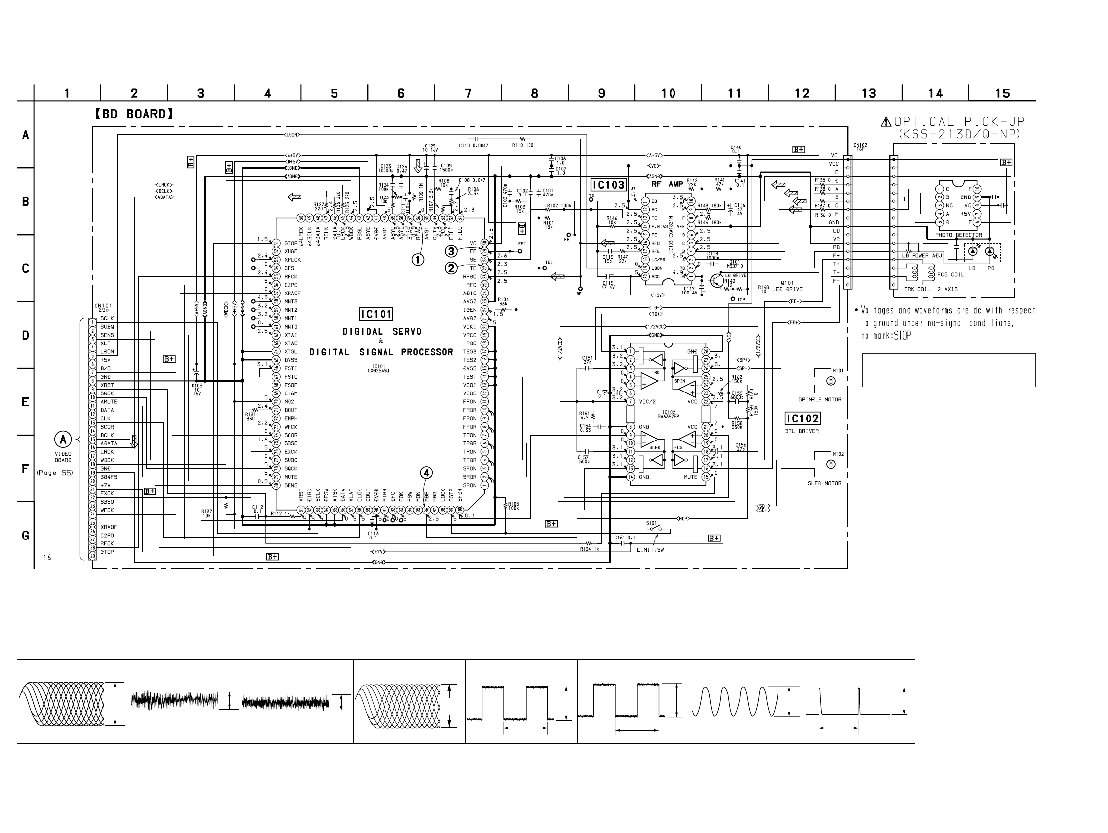
6-5. SCHEMATIC DIAGRAM – BD SECTION – • See page 83 for IC Block Diagrams.
The components identified by mark ! or dotted
line with mark ! are critical for safety.
Replace only with part number specified.
• Waveform
1 IC101 @§ (RFDC)
Approx. 1.3Vp-p
2 IC101 @¶ (TEI)
(PLAY MODE)
Approx. 0.5Vp-p
3 IC101 @ª (FE)
(PLAY MODE)
Approx. 0.2Vp-p
4 IC101 #§ (RFAC)
5 IC101 $∞ (LRCK)
+0.25
1.3
–0.20
Vp-p
22.7 µsec
5.2Vp-p
6 IC101 $¶ (BCLK)
474 nsec
5.2Vp-p
7 IC101 ^™ (XTAI)
16.9344MHz
5.2Vp-p
8 IC103 (§ (MDP)
— 31 — — 32 —
7.5 µsec
2.4Vp-p
HCD-V3900/V5900
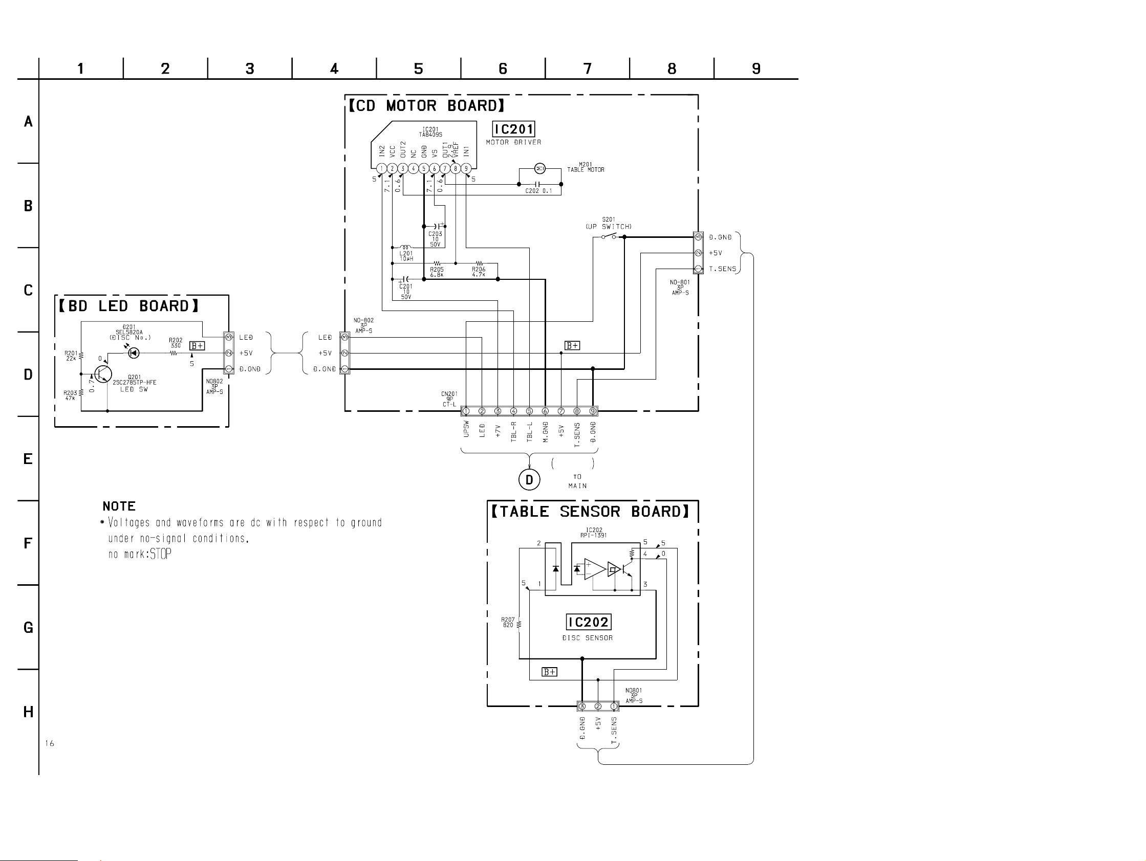
6-7. SCHEMATIC DIAGRAM – CD MOTOR SECTION – • See page 84 for IC Block Diagrams.
Page 47
— 35 — — 36 —
HCD-V3900/V5900
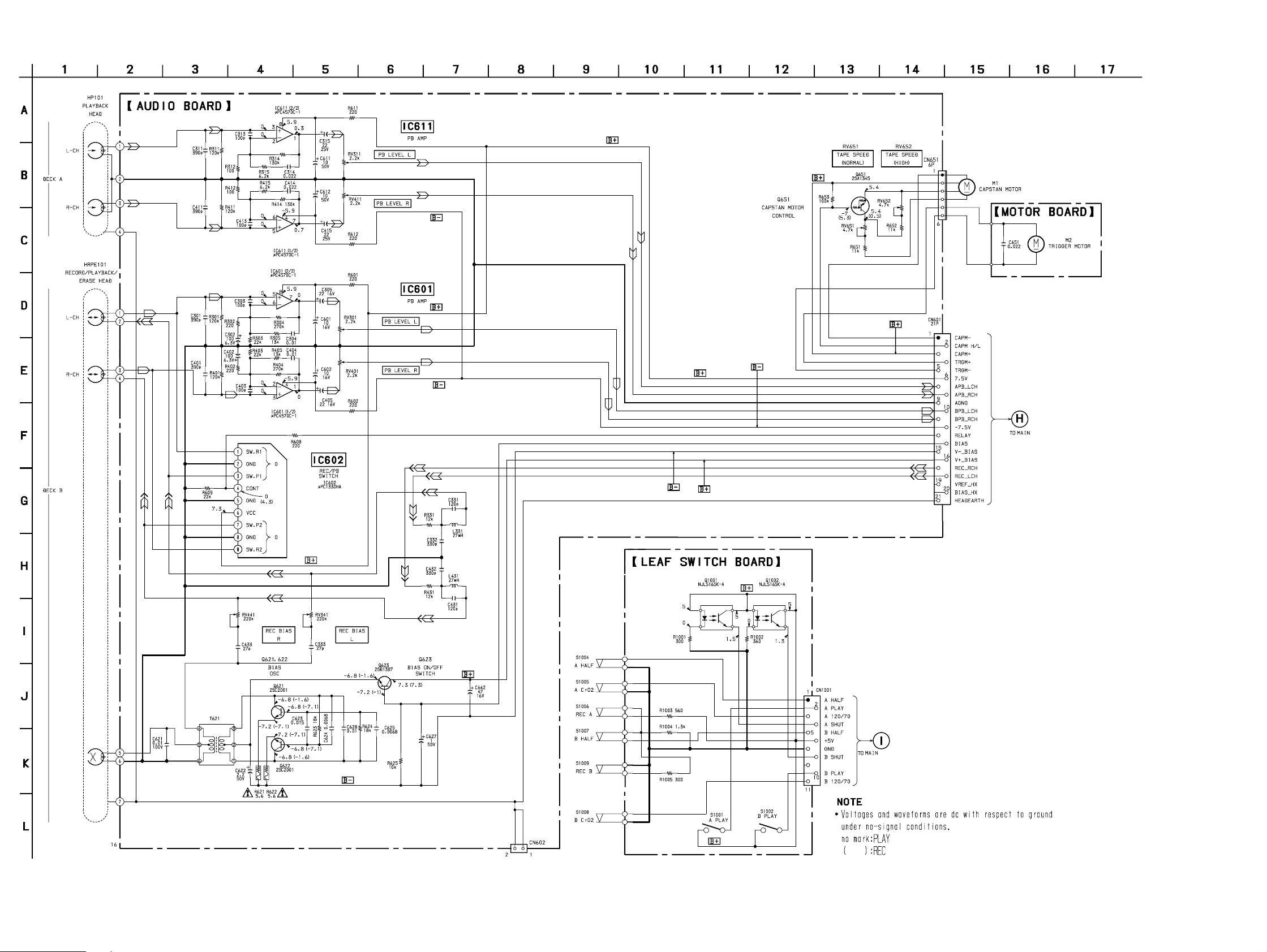
6-9. SCHEMATIC DIAGRAM – AUDIO SECTION – • See page 84 for IC Block Diagrams.
(Page 49)
(Page 49)
— 39 — — 40 —
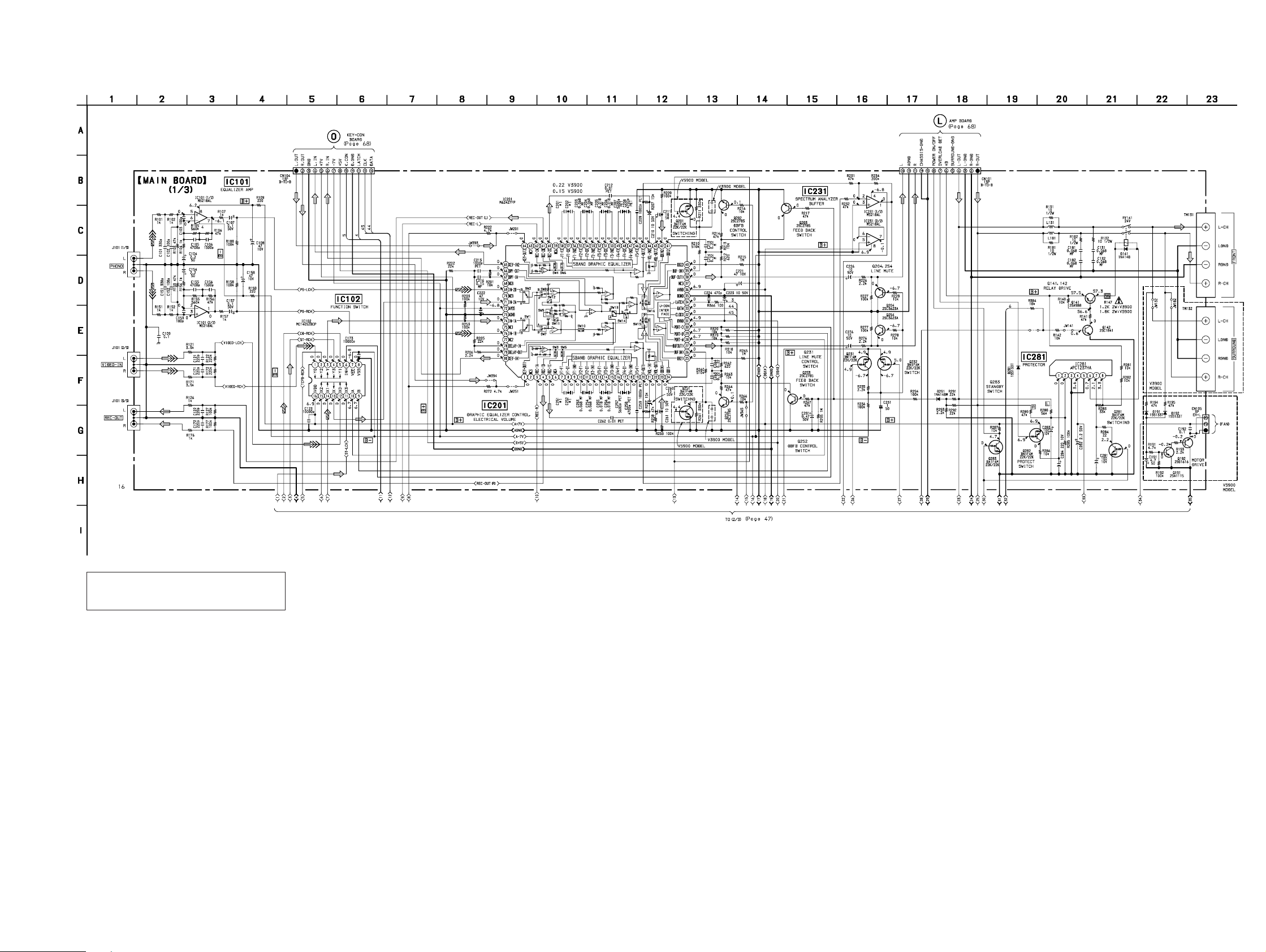
6-12. SCHEMATIC DIAGRAM – MAIN SECTION (1/3) – • See page 87 for IC Block Diagrams.
HCD-V3900/V5900
The components identified by mark ! or dotted
line with mark ! are critical for safety.
Replace only with part number specified.
— 45 — — 46 —
 Loading...