

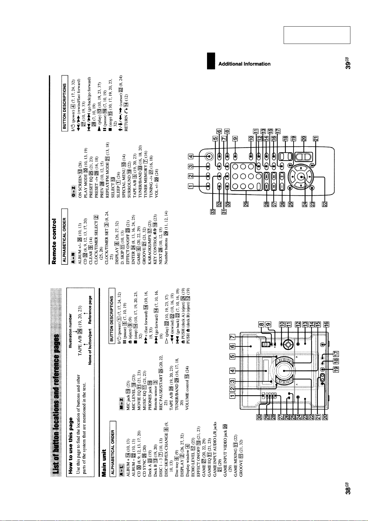
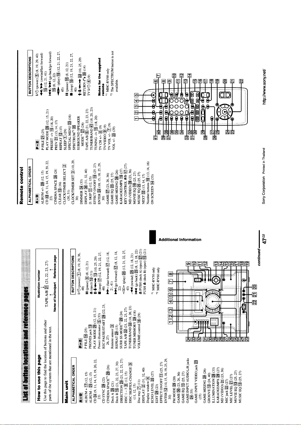
Sony HCD-RV20, HCD-RV50, HCD-RV60 Service Manual
HCD-RV20/RV50/RV60
SERVICE MANUAL
Ver 1.0 2003. 05
• HCD-RV20/RV50/RV60 is the
tuner, deck, CD and amplifier
section in MHC-RV20/RV50/RV60.
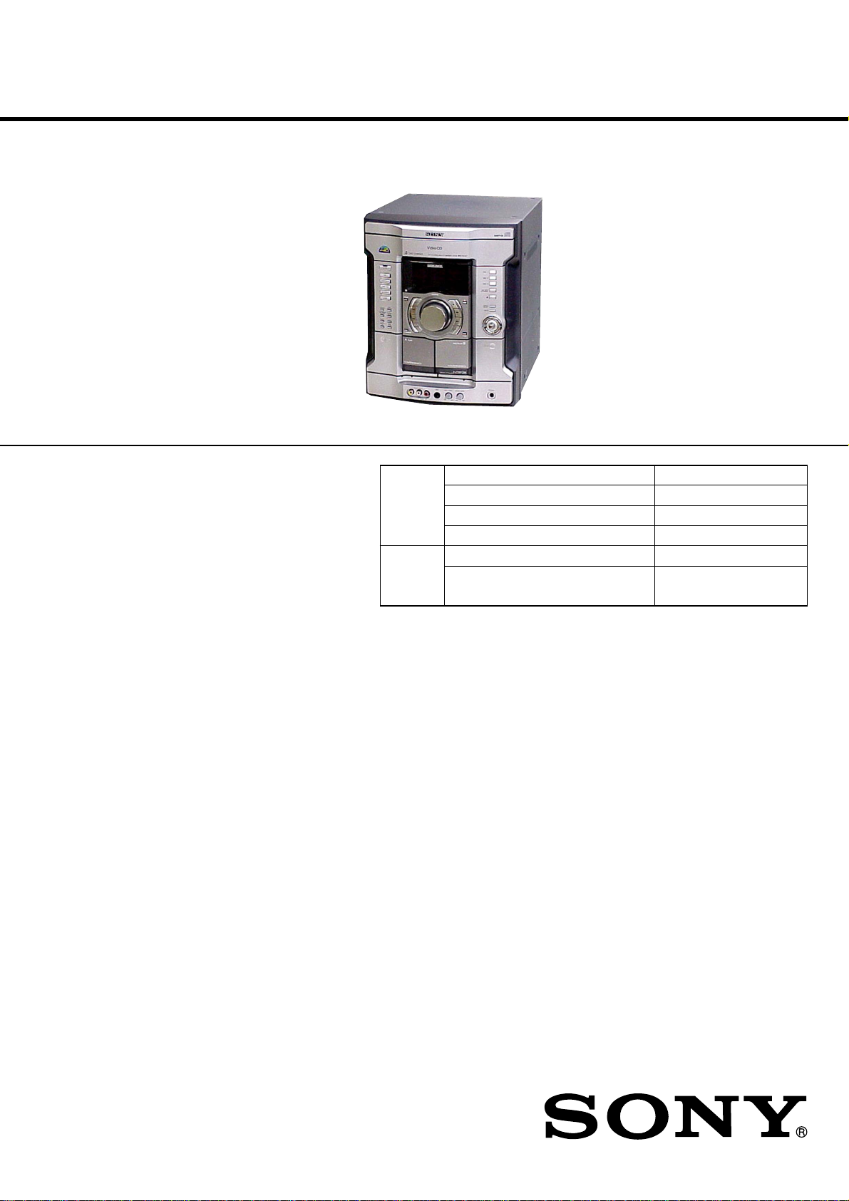
(Photo: HCD-RV50)
Model Name Using Similar Mechanism NEW
CD CD Mechanism Type CDM74-30BD62
Section Base Unit Name BU-30BD62
Optical Pick-up Name A-MAX.3
Tape Deck
Section Tape Transport Mechanism Type
Model Name Using Similar Machanism NEW
E Model
RV20: CWM43FF-13
RV50/RV60: CWM43RR-23
Amplifier section
HCD-RV20:
The following measured at AC 120, 127, 220, 240 V,
50/60 Hz
DIN power output (rated):
80 + 80 watts
(6 ohms at 1 kHz, DIN)
Continuous RMS power output (reference):
100 + 100 watts (6 ohms at
1 kHz, 10% THD)
HCD-RV60:
Front speaker
The following measured at AC 120, 127, 220, 240 V,
50/60 Hz
DIN power output (rated):
160 + 160 watts
(6 ohms at 1 kHz, DIN)
Continuous RMS power output (reference):
200 + 200 watts (6 ohms at
1 kHz, 10% THD)
Music power output (reference):
400 + 400 watts (6 ohms at
1 kHz, 10% THD)
HCD-RV50:
The following measured at AC 120, 127, 220, 240 V,
50/60 Hz
DIN power output (rated):
115 + 115 watts
(6 ohms at 1 kHz, DIN)
Continuous RMS power output (reference):
140 + 140 watts (6 ohms at
1 kHz, 10% THD)
SPECIFICATIONS
Inputs
HCD-RV20:
GAME INPUT AUDIO L/R (phono jacks):
voltage 250 mV,
impedance 47 kilohms
GAME INPUT VIDEO (phono jack):
1 Vp-p, 75 ohms
MIC (phone jack): sensitivity 1 mV,
impedance 10 kilohms
Outputs
PHONES (stereo mini jack):
accepts headphones of
8 ohms or more
VIDEO OUT (phono jack):
max. output level
1 Vp-p, unbalanced, Sync
negative, load impedance
75 ohms
SPEAKER: accepts impedance of 6 to
16 ohms
– Continued on next page –
COMPACT DISC DECK RECEIVER
9-877-378-01
2003E04-1
© 2003. 05
Sony Corporation
Home Audio Company
Published by Sony Engineering Corporation
1

HCD-RV20/RV50/RV60
HCD-RV50/RV60:
MD (VIDEO) IN L/R (phono jacks):
voltage 450/250 mV,
impedance 47 kilohms
GAME INPUT AUDIO L/R (phono jacks):
voltage 250 mV,
impedance 47 kilohms
GAME INPUT VIDEO (phono jack):
1 Vp-p, 75 ohms
MIC (phone jack): sensitivity 1 mV,
impedance 10 kilohms
Outputs
PHONES (stereo mini jack):
accepts headphones of
8 ohms or more
VIDEO OUT (phono jack):
max. output level 1 Vp-p,
unbalanced, Sync
negative, load impedance 75 ohms
MD (VIDEO) OUT L/R (phono jacks):
impedance 1 kilohms
SPEAKER: accepts impedance of 6 to
16 ohms
SURROUND SPEAKER (HCD-RV60 only)
accepts impedance of 24
ohms
CD player section
System Compact disc and digital
audio system
Laser Semiconductor laser
(λ=780 nm)
Emission duration:
continuous
Frequency response 2 Hz – 20 kHz (±0.5 dB)
Wavelength 780 – 790 nm
Signal-to-noise ratio More than 90 dB
Dynamic range More than 90 dB
Video color system format
NTSC, PAL
Tape deck section
Recording system 4-track 2-channel stereo
Frequency response 50 – 13,000 Hz (±3 dB),
using Sony TYPE I
cassettes
Wow and flutter ±0.15% W.Peak (IEC)
0.1% W.RMS (NAB)
±0.2% W.Peak (DIN)
Tuner section
FM stereo, FM/AM superheterodyne tuner
FM tuner section
Tuning range 87.5 – 108.0 MHz
Antenna FM lead antenna
Antenna terminals 75 ohms unbalanced
Intermediate frequency 10.7 MHz
AM tuner section
Tuning range
Middle Eastern model: 531 – 1,602 kHz (with the tuning
interval set at 9 kHz)
Other models: 530 – 1,710 kHz (with the tuning
interval set at 10 kHz)
531 – 1,602 kHz (with the tuning
interval set at 9 kHz)
Antenna AM loop antenna
Antenna terminals External antenna terminal
Intermediate frequency 450 kHz
Front speaker SS-RV990 for HCD-RV60/RV50:
Speaker system 3-way, 3-unit, bass-reflex
type
Speaker units
Sub Woofer: 15 cm, cone type
Woofer: 15 cm, cone type
Tweeter: 5 cm, cone type
Nominal impedance 6 ohms
Dimensions (w/h/d) Approx. 240 × 363 × 290 mm
Mass Approx. 4.7 kg net per
speaker
Surround speaker SS-RSV60 for HCD-RV60:
Speaker system 3-way, 3-unit, bass-reflex
type
Speaker units
Woofer: 13 cm, cone type
Tweeter: 5 cm, cone type
Super tweeter: 2 cm, dome type
Nominal impedance 24 ohms
Dimensions (w/h/d) Approx. 195 × 325 × 225 mm
Mass Approx. 2.3 kg net per
speaker
General
Power requirements
Saudi Arabian model: 120 – 127 V/220 V or
230 – 240 V AC,
50/60 Hz
Adjustable with voltage
selector
Thai model: 220 V AC, 50/60 Hz
Other models: 120 V, 220 V or 230 –
240 V AC, 50/60 Hz
Adjustable with voltage
selector
Power consumption
HCD-RV20: 110 watts
HCD-RV50: 135 watts
HCD-RV60: 190 watts
Dimensions (w/h/d)
HCD-RV20: Approx. 280 × 325 × 407 mm
HCD-RV50/RV60: Approx. 280 × 325 × 407 mm
Mass
HCD-RV20: Approx. 8.5 kg
HCD-RV50: Approx. 9.0 kg
HCD-RV60: Approx. 11.5 kg
Supplied accessories: AM loop antenna (1)
Remote Commander (1)
Batteries (2)
FM lead antenna (1)
Speaker pads
HCD-RV20 (8)
HCD-RV50 (8)
HCD-RV60 (16)
Video cable (1)
Design and specifications are subject to change without
notice.
Speaker
HCD-RV20:
Speaker system 3-way, 3-unit,
bass-reflex type
Speaker units
Woofer: 13 cm, cone type
Sub woofer: 13 cm, cone type
Tweeter: 5 cm, cone type
Nominal impedance 6 ohms
Dimensions (w/h/d) Approx. 240 × 325 × 243 mm
Mass Approx. 4.3 kg net per
speaker
2
SAFETY-RELATED COMPONENT WARNING!!
COMPONENTS IDENTIFIED BY MARK 0 OR DOTTED LINE
WITH MARK 0 ON THE SCHEMATIC DIAGRAMS AND IN
THE PARTS LIST ARE CRITICAL TO SAFE OPERATION.
REPLACE THESE COMPONENTS WITH SONY P ARTS WHOSE
PART NUMBERS APPEAR AS SHOWN IN THIS MANUAL OR
IN SUPPLEMENTS PUBLISHED BY SONY.

HCD-RV20/RV50/RV60
CAUTION
Use of controls or adjustments or performance of procedures
other than those specified herein may result in hazardous
radiation exposure.
Notes on Chip Component Replacement
• Never reuse a disconnected chip component.
• Notice that the minus side of a tantalum capacitor may be
damaged by heat.
Flexible Circuit Board Repairing
• Keep the temperature of soldering iron around 270°C during
repairing.
• Do not touch the soldering iron on the same conductor of the
circuit board (within 3 times).
• Be careful not to apply force on the conductor when soldering
or unsoldering.
NOTES ON HANDLING THE OPTICAL PICK-UP BLOCK
OR BASE UNIT
The laser diode in the optical pick-up block may suffer electrostatic
breakdown because of the potential difference generated by the
charged electrostatic load, etc. on clothing and the human body.
During repair, pay attention to electrostatic break-down and also
use the procedure in the printed matter which is included in the
repair parts.
The flexible board is easily damaged and should be handled with
care.
NOTES ON LASER DIODE EMISSION CHECK
The laser beam on this model is concentrated so as to be focused on
the disc reflective surface by the objective lens in the optical pickup block. Therefore, when checking the laser diode emission,
observe from more than 30 cm away from the objective lens.
Laser component in this product is capable
of emitting radiation exceeding the limit for
Class 1.
MODEL IDENTIFICATION
– BACK PANEL –
PARTS No.
MODEL PARTS No.
RV20: E3, E15, SP, MY, PL 4-264-151-0s
RV20: EA 4-264-151-1s
RV50: E3, E15, SP, MY, PL 4-264-151-2s
RV50: EA 4-264-151-3s
RV60: EA 4-264-151-4s
RV60: E3, E15, SP, MY, PL 4-264-151-5s
RV20: TH 4-264-151-6s
RV50: TH 4-264-151-7s
RV60: TH 4-264-151-8s
• Abbreviation
E3 : 240 V AC area in E model
EA : Saudi Arabia model
MY : Malaysia model
SP : Singapore model
TH : Thai model
SETTING AND RELEASING THE CD DISC TRAY LOCK
FUNCTION
This set has a disc tray lock function to prevent discs for
demonstration at shops from theft. While this lock function is set,
the tray will not be delivered out even when the OPEN/CLOSE
button is pressed.
Setting method:
Press the OPEN/CLOSE button while pressing the STOP button.
After a few seconds, the message “LOCKED” will appear on the
fluorescent indicator tube with the tray locked.
Releasing method:
Just as the lock is set, press the OPEN/CLOSE button while
pressing the STOP button.
After a few seconds, the message “UNLOCKED” will appear with
the lock released.
3

HCD-RV20/RV50/RV60
TABLE OF CONTENTS
1. GENERAL
HCD-RV20 Main Unit ............................................................5
HCD-RV20 Remote Control ................................................... 5
HCD-RV50/RV60 Main Unit .................................................. 6
HCD-RV50/RV60 Remote Control ......................................... 6
2. DISASSEMBLY
2-1. Case (Top) ...........................................................................8
2-2. CD Door .............................................................................. 8
2-3. CD Mechanism Block ......................................................... 9
2-4. Front Panel Section ........................................................... 10
2-5. Tape Mechanism Deck ...................................................... 11
2-6. Panel Board, 1 Stream Led Board,
6 Stream Led Board, Remote Board ................................. 11
2-7. Jack Board ......................................................................... 12
2-8. Back Panel Section............................................................ 12
2-9. Main Board ....................................................................... 13
2-10. Power Amp Board ............................................................. 13
2-11. Video Board, SW Board, Driver Board.............................14
2-12. CD Block Assy.................................................................. 14
2-13. Sensor Board ..................................................................... 15
2-14. Motor (TB) Board ............................................................. 15
2-15. Motor (LD) Board ............................................................. 16
2-16. BD Board .......................................................................... 16
3. DIAGRAMS
3-1. IC Pin Description.............................................................17
3-2. Circuit Boards Location .................................................... 19
3-3. Printed Wiring Board –CD Mechanism Section (1/2)– .... 20
3-4. Schematic Diagram –CD Mechanism Section (1/2)– ....... 21
3-5. Printed Wiring Boards –CD Mechanism Section (2/2)– ... 22
3-6. Schematic Diagram –CD Mechanism Section (2/2)– ....... 23
3-7. Printed Wiring Board –Video Section–............................. 24
3-8. Schematic Diagram –Video Section (1/2)–....................... 26
3-9. Schematic Diagram –Video Section (2/2)–....................... 27
3-10. Printed Wiring Board –Main Section– .............................. 28
3-11. Schematic Diagram –Main Section (1/3)– ........................ 29
3-12. Schematic Diagram –Main Section (2/3)– ........................ 30
3-13. Schematic Diagram –Main Section (3/3)– ........................ 31
3-14. Printed Wiring Boards –Panel Section– ............................ 32
3-15. Schematic Diagram –Panel Section– ................................ 33
3-16. Printed Wiring Boards –Jack Section–..............................34
3-17. Schematic Diagram –Jack Section– .................................. 35
3-18. Printed Wiring Board –Power Amp Section– ................... 36
3-19. Schematic Diagram –Power Amp Section (1/2)– ............. 37
3-20. Schematic Diagram –Power Amp Section (2/2)– ............. 38
3-21. Printed Wiring Board
–Transformer Section (HCD-RV20)– ............................... 39
3-22. Printed Wiring Board
–Transformer Section (HCD-RV50)– ............................... 40
3-23. Printed Wiring Board
–Transformer Section (HCD-RV60)– ............................... 41
3-24. Schematic Diagram –Transformer Section– ..................... 42
3-25. IC Block Diagrams............................................................ 43
4. EXPLODED VIEWS
4-1. Main Section .....................................................................46
4-2. Front Panel Section (1)...................................................... 47
4-3. Front Panel Section (2)...................................................... 48
4-4. Front Panel Section (3)...................................................... 49
4-5. Main Board Section .......................................................... 50
4-6. CD Mechanism Deck Section (1) ..................................... 51
4-7. CD Mechanism Deck Section (2) ..................................... 52
4-8. Optical Pick-up Section..................................................... 53
5. ELECTRICAL PARTS LIST ........................................ 54
4
• HCD-RV20
SECTION 1
GENERAL
HCD-RV20/RV50/RV60
This section is extracted
from instruction manual.
Main Unit
5
HCD-RV20/RV50/RV60
• HCD-RV50/RV60
Main Unit
6
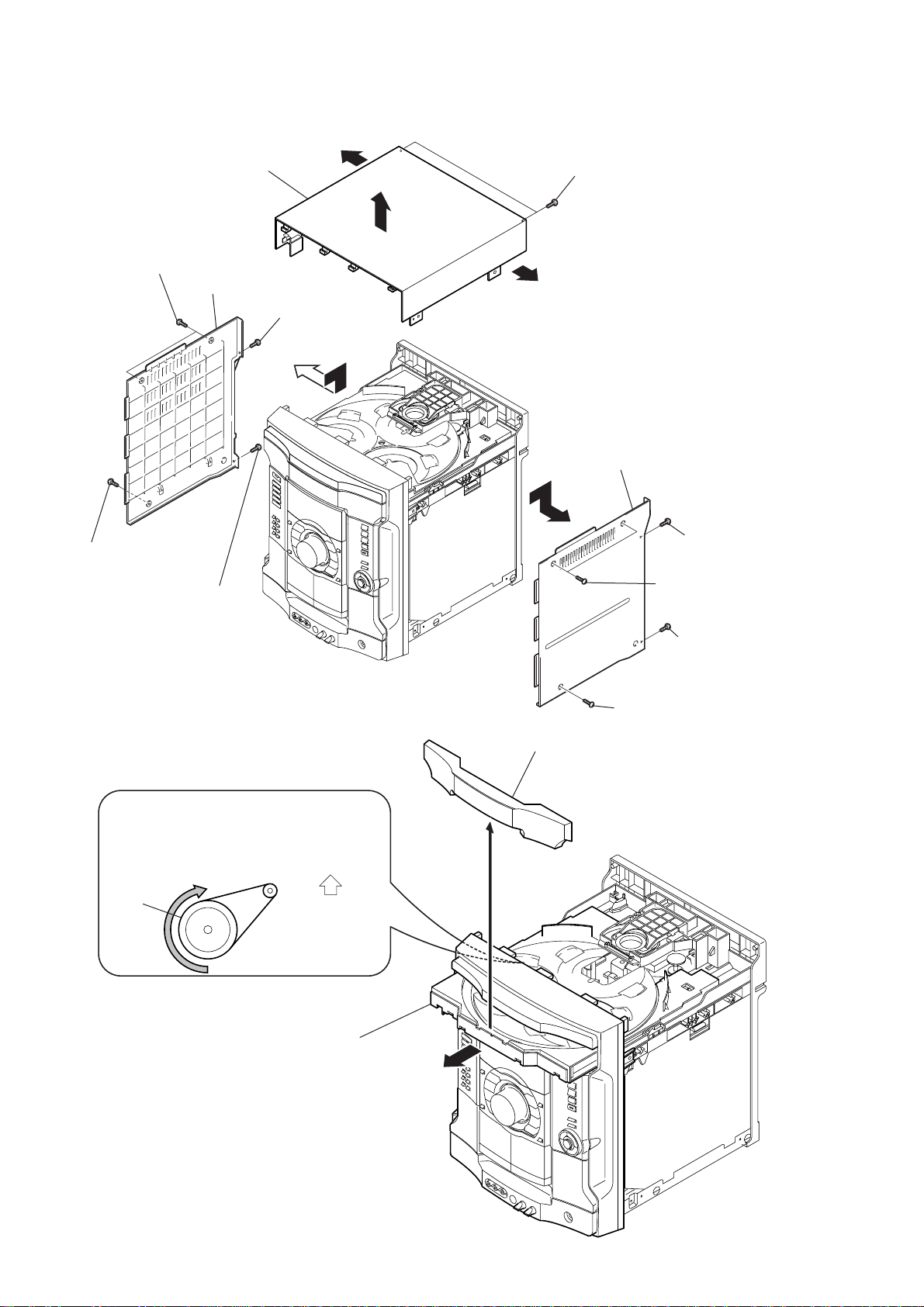
Note : Disassemble the unit in the order as shown below.
SET
2-1. CASE (TOP)
(Page 8)
2-2. CD DOOR
(Page 8)
2-3. CD MECHANISM BLOCK
(Page 9)
2-11. VIDEO BOARD,
SW BOARD,
DRIVER BOARD
(Page 14)
2-13. SENSOR BOARD
2-14. MOTOR (TB) BOARD
2-15. MOTOR (LD) BOARD
SECTION 2
DISASSEMBLY
(Page 15)
(Page 15)
(Page 16)
HCD-RV20/RV50/RV60
2-12. CD BLOCK ASSY
(Page 14)
2-16. OPTICAL PICK-UP,
BD BOARD
(Page 16)
2-4. FRONT PANEL SECTION
(Page 10)
2-6. PANEL BOARD,
1 STREAM LED BOARD,
6 STREAM LED BOARD,
REMOTE BOARD
(Page 11)
2-5. TAPE MECHANISM DECK
2-7. JACK BOARD
2-8. BACK PANEL SECTION
(Page 12)
2-9. MAIN BOARD
(Page 13)
2-10. POWER AMP BOARD
(Page 13)
(Page 11)
(Page 12)
7
HCD-RV20/RV50/RV60
)
Note : Follow the disassembly procedure in the numerical order given.
2-1. CASE (TOP)
6
two screws (case 3 TP2)
7
screw (case 3 TP2)
9
(+BVTP 3
qf
case (side-L)
screw
case (top)
×
10)
qs
8
screw
(+BVTP 3
×
q;
10)
qd
qs
qa
two screws (+BVTP 3
case (side-R)
5
×
10)
3
screw
(+BVTP 3
1
two screws
(case 3 TP2)
×
10
2-2. CD DOOR
CD mechanism deck (CDM74-30BD62)
1
Turn the pulley to the direction of arrow.
pulley
Front panel side
2
Pull-out the disc tray.
3
4
CD door
4
(+BVTP 3
2
screw (case 3 TP2)
screw
×
10)
8
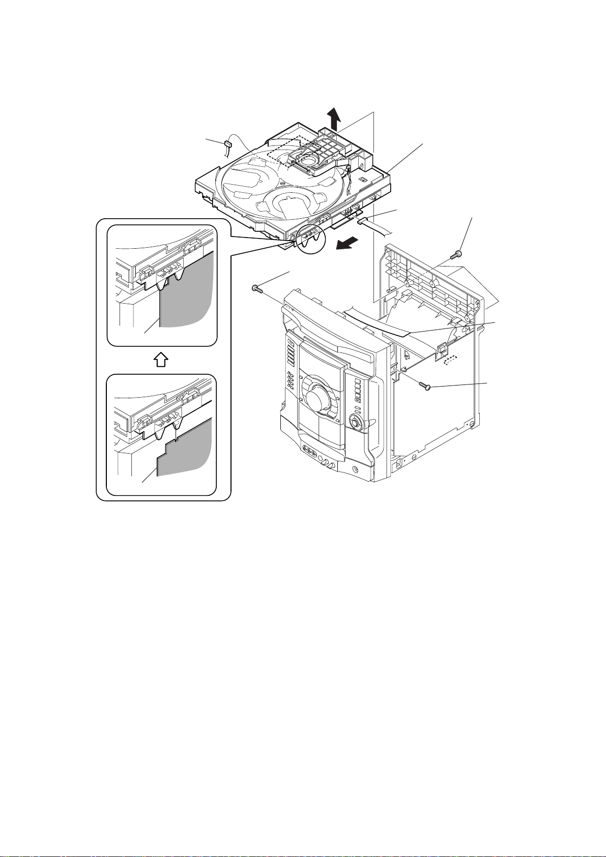
2-3. CD MECHANISM BLOCK
)
1
CN301
6
4
screw
(+BVTP 3
HCD-RV20/RV50/RV60
7
9
CD mechanism block
2
CN701
×
10)
3
three
(+BVTP 3
screws
×
10)
MAIN board
MAIN board
8
CN312
(flat type)
5
screw
(+BVTP 3
×
10
9
HCD-RV20/RV50/RV60
)
2-4. FRONT PANEL SECTION
7
screw
(+BVTP 3
3
×
8)
TRANS board
CN311
(flat type)
1
CN003
4
CN308
0
front panel section
6
connector
5
connector
9
three screws (+BVTP 3
2
CN304
(flat type)
× 8
8
screw
(+BVTP 3
)
×
8
10
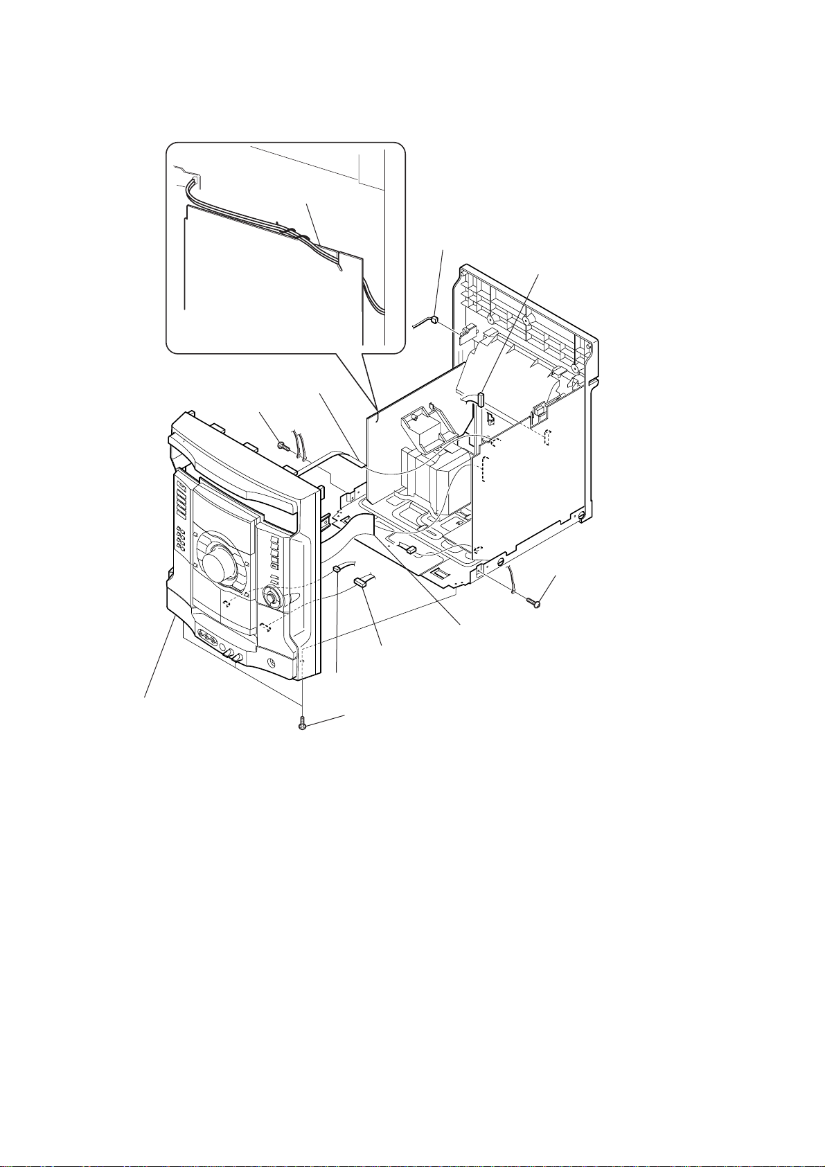
2-5. TAPE MECHANISM DECK
)
)
1
connector
2
(+BVTP 2.6
5
tape mechanism deck
two
screws
3
(+BVTP 2.6
HCD-RV20/RV50/RV60
×
8)
three
screws
×
8)
4
two
screws
(+BVTP 2.6
×
8
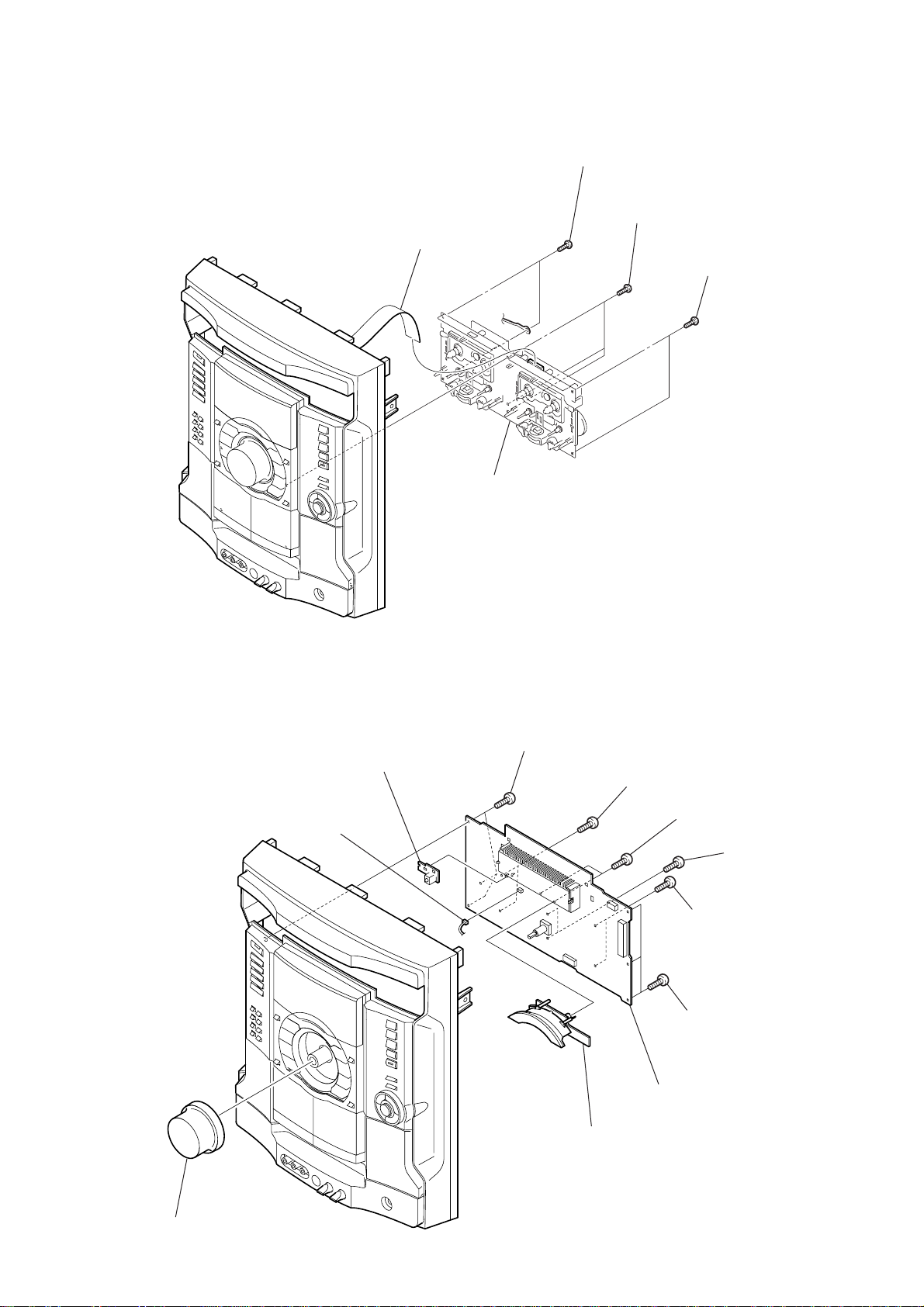
2-6. PANEL BOARD, 1 STREAM LED BOARD, 6 STREAM LED BOARD, REMOTE BOARD
5
three
screws
×
8)
6
two
screws
(+BVTP 2.6
7
9
1 STREAM LED board (RV20)
6 STREAM LED board (RV50/RV60)
×
8
two
(+BVTP 2.6
3
two
(+BVTP 2.6
2
three
(+BVTP 2.6
PANEL board
8)
screws
4
(+BVTP 2.6
screws
screws
0
CN607
qa
REMOTE board
(+BVTP 2.6
two
×
8)
screws
×
×
×
8
8)
8)
1
volume knob
11
HCD-RV20/RV50/RV60
2-7. JACK BOARD
1
two
screws
(+BVTP 2.6
4
shield plate
6
×
8)
JACK board
2-8. BACK PANEL SECTION
6
back panel section
5
2
screw
(+BVTP 3
×
3
screw
(+BVTP 3
8)
5
two mic knobs
1
CN101
(flat type)
×
8)
4
three
(+BVTP 3
screws
×
10)
12
chassis section
2
CN303
3
two
screws
(+BVTP 3
×
10)

2-9. MAIN BOARD
d
d
MAIN board
HCD-RV20/RV50/RV60
2
MAIN boar
2-10. POWER AMP BOARD
1
CN902
4
(+BVTP 3
5
screw
(+BVTP 3
screw
×
8)
×
1
two
screws
×
×
10)
10)
(+BVTP 3
3
screw
(+BVTT 3
8)
×
10)
two claws
2
screw
(+BVTT 3
6
POWER AMP boar
13
HCD-RV20/RV50/RV60
d
2-11. VIDEO BOARD, SW BOARD, DRIVER BOARD
5
SW board
0
CN702 (flat type)
7
CN703
2
two
(+BVTP 3
9
DRIVER board
3
1
CN101 (flat type)
screws
×
10)
VIDEO boar
2-12. CD BLOCK ASSY
6
4
screw
(+BTTP (M2.6))
qa
9
8
two
coil springs
(insulator)
7
two stoppers (BU)
CN704
2
holder (30) assy
CD block assy
two
insulators
(BU-30)
8
two
screws
(+BTTP (M2.6))
0
1
floating
(+PTPWH M2.6)
5
two
insulators
(BU-30)
two
4
(insulator)
3
two floating
(+PTPWH M2.6)
screw
coil springs
screws
14
6
two screws
(BVTT M2.6)
2-13. SENSOR BOARD
2
tray
1
floating
(+PTPWH M2.6)
6
floating
(+PTPWH M2.6)
7
gear (geneva)
screw
8
screw
(+BTTP (M2.6))
screw
9
SENSOR board
0
CN731
HCD-RV20/RV50/RV60
3
belt (table)
4
floating
(+PTPWH M2.6)
5
screw
pulley (table)
2-14. MOTOR (TB) BOARD
1
5
table motor assy (M741)
3
MOTOR (TB) board
4
Remove the two solderings of motor.
2
two
screws
(+BTTP (M2.6))
15
HCD-RV20/RV50/RV60
2-15. MOTOR (LD) BOARD
4
Remove the two solderings of motor.
5
loading motor assy (M751)
2
two
screws
(+BTTP (M2.6))
3
MOTOR (LD) board
2-16. BD BOARD
1
belt (loading)
1
CN102 (flat type)
4
BD board
16
2
Remove the two solderings of motor.
3
Remove the two solderings of motor.
HCD-RV20/RV50/RV60
SECTION 3
DIAGRAMS
3-1. IC PIN DESCRIPTION
• IC601 LC876696B-5IG9 (SYSTEM CONTROL, FLD CONTROL) (PANEL BOARD) (RV20)
• IC601 LC876696B-5IH0 (SYSTEM CONTROL, FLD CONTROL) (PANEL BOARD) (RV50/RV60)
Pin No. Pin Name I/O Pin Description
1 SYS MUTE O System mute signal output
2BU1924 DATA I Not used in this set. (Connected to ground.)
3 PWR DOWN I Power down signal input
4 LC78646 RESET O CD reset signal output
5 LC78646 CE O CD CE signal output
6 LC78646 CE (MP3) O CD CE (MP3) signal output
7 M61519 CLK O Clock signal output
8BU2099FV LCK O LCK signal output
9 LC72121 CE O CE signal output
10 LC78684 SYNC I SYNC signal input
11 RESET I Reset signal input from the IC603
12 XT1 I Oscillater connect pin (32.768 kHz)
13 XT2 O Oscillater connect pin (32.768 kHz)
14 VSS1 — Ground pin
15 CF1 I Ceramic vibrator connect pin (8.64 MHz)
16 CF2 O Ceramic vibrator connect pin (8.64 MHz)
17 VDD — Power supply pin (+3.3 V)
18 TAPE A STAT I Tape A start signal input
19 TAPE B STAT I Tape B start signal input
20 CD ENCODER I CD encoder switch signal input
21 SW ON/OFF SENSOR I Switch control on/off signal input
22 STREAM IN I Stream in signal input
23 VACS I VACS signal input
24 KEY2 I Key signal input 2
25 KEY1 I Key signal input 1
26 KEY0 I Key signal input 0
27 PROTECTOR (HOLD) I Protector (Hold) signal input
28 REMOCON IN I Remote control signal input from the RM601
29 BU1924 CLK I Not used in this set. (Connected to ground.)
30 – 41 G12 – G1 O FLD control signal output
42 – 45 P1 – P4 O FLD control signal output
46 VDD3 — Power supply pin (+3.3 V)
47 – 50 P5 – P8 O FLD control signal output
51 VPP — Ground pin
52 – 55 P9 – P12 O FLD control signal output
56 SW1 (a) P13 O FLD control signal output
57 SW2 (b) P14 O FLD control signal output
58 SW3 (c) P15 O FLD control signal output
59 SW4 (d) P16 O FLD control signal output
60 SW5 P17 O FLD control signal output
61 SW6 P18 O FLD control signal output
62 SW7 P19 O FLD control signal output
63 SW8 P20 O FLD control signal output
64, 65 P21, P22 O FLD control signal output
66 ENTER LED O Not used in this set. (Open)
67 MD/VIDEO LED O RV20: Not used. (Open) RV50/RV60: GAME LED (LED610) drive signal output
68 GAME LED O
69 TAPE LED O TAPE A/B LED (LED609) drive signal output
70 TUNER LED O TUNER/BAND LED (LED608) drive signal output
RV20: GAME LED (LED612) drive signal output
RV50/RV60: MD/VIDEO LED (LED612) drive signal output
17
HCD-RV20/RV50/RV60
Pin No. Pin Name I/O Pin Description
71 CD LED O CD LED (LED607) drive signal output
72 VDD4 — Power supply pin (+3.3 V)
73 CD VDD — CD power supply pin
74 TUNER TUNED I Tuner tuning signal input from the TU701 (tuner pack)
75 TUNER STEREO I Tuner stereo signal input from the TU701 (tuner pack)
76 CD DRF I CD DRF signal input
77 CD WRQ I CD WRQ signal input
78 CD NUMBER SENSOR I CD number sensor signal input
79 TAPE AMS IN I T ape AMS signal input
80 VR ENCODER A I VR encoder (VR601) signal input
81 VR ENCODER B I VR encoder (VR601) signal input
82 TAPE REEL A I Tape reel A signal input
83 TAPE REEL B I Tape reel B signal input
84 MODE SW IN I Mode switch signal input
85 STREAM 1 LED O Stream LED drive signal output
86 STREAM 2 LED/CD MUTE O RV20: CD mute signal output RV50/RV60: Stream LED drive signal output
87 STREAM 3 LED O RV20: Not used. (Open) RV50/RV60: Stream LED drive signal output
88
89 VSS2 — Ground pin
90 VDD2 — Power supply pin (+3.3 V)
91
92
93 POWER LED O POWER LED (LED614) drive signal output
94 POWER RELAY O Power relay signal output
95
96 LC72121 DI I Serial data signal input
97 LC72121/BU2099FV CLK O Serial clock signal output
98 LC78646/LC78684 DO O Serial data signal output
99 LC78646/LC78684 DI I Serial data signal input
100 LC78646/LC78684 CLK O Serial clock signal output
STREAM 4 LED/
MECHA VCC RV50/RV60: Stream LED drive signal output
STREAM 5 LED/
TAPE SOL A RV50/RV60: Stream LED drive signal output
STREAM 6 LED/
TAPE SOL B RV50/RV60: Stream LED drive signal output
LC72121/M61529/
BU2099FV DO
RV20: Mechanism power control signal output “L”: ON, “H”: OFF
O
RV20: Tape SOL A control signal output “L”: ON, “H”: OFF
O
RV20: Tape SOL B control signal output “L”: ON, “H”: OFF
O
O Serial data signal output
18
HCD-RV20/RV50/RV60
d
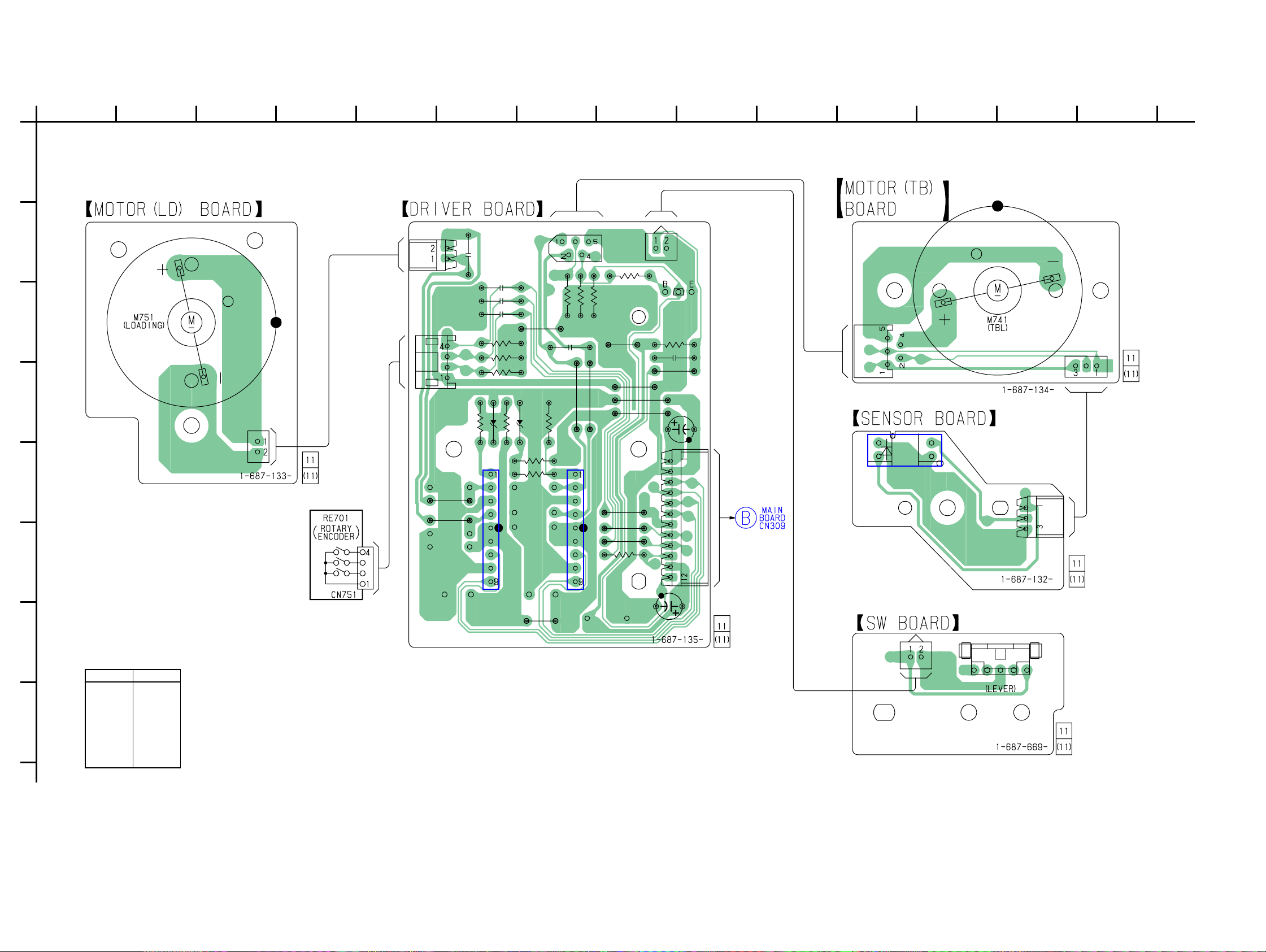
3-2. CIRCUIT BOARDS LOCATION
TRANS board
MOTOR (LD) board
PANEL board
REMOTE board
1 STREAM LED board (RV20)
6 STREAM LED board (RV50/RV60)
JACK board
VIDEO board
SW board
VIDEO OUT board
SENSOR board
POWER AMP board
BD board
DRIVER board
MOTOR (TB) boar
MAIN board
THIS NOTE IS COMMON FOR PRINTED WIRING
BOARDS AND SCHEMATIC DIAGRAMS.
(In addition to this, the necessary note is
printed in each block.)
for schematic diagram:
• All capacitors are in µF unless otherwise noted. pF: µµF
50 WV or less are not indicated except for electrolytics
and tantalums.
• All resistors are in Ω and 1/
specified.
•%: indicates tolerance.
f
•
• C : panel designation.
Note: The components identified by mark 0 or dotted line
• A : B+ Line.
• B : B– Line.
• H : adjustment for repair.
•Voltage and waveforms are dc with respect to ground
•Voltages are taken with a VOM (Input impedance 10 MΩ).
•Waveforms are taken with a oscilloscope.
• Circled numbers refer to waveforms.
• Signal path.
for printed wiring boards:
• X : parts extracted from the component side.
• Y : parts extracted from the conductor side.
• x : parts mounted on the conductor side.
• : Pattern from the side which enables seeing.
: internal component.
with mark 0 are critical for safety.
Replace only with part number specified.
under no-signal (detuned) conditions.
Voltage variations may be noted due to normal produc-
tion tolerances.
no mark : FM
(): CD
[]: TAPE
Voltage variations may be noted due to normal production tolerances.
F : FM
f : AM
E : PB (DECK A)
d : PB (DECK B)
G : REC (DECK B)
J : CD
c : digital out
L : VIDEO
(The other layer’s patterns are not indicated.)
4
W or less unless otherwise
•Waveforms
– BD Board –
1
IC103
(A), 8 (C)
6
2
IC103
(B), 9 (D)
7
3
IC103
(RFAC)
qg
4
IC103
– VIDEO Board –
(RFDCO)
wk
1
33.8688MHz
IC505
(XTAO)
<zb/>
2
29MHz
IC505
(CLKA)
<x/n>
Approx.
160mVp-p
Approx.
160mVp-p
Approx.
1Vp-p
Approx.
0.6Vp-p
1.1Vp-p
0.6Vp-p
– PANEL Board –
1
1.2Vp-p
32.768kHz
qs
(XT1)
IC601
2
1Vp-p
8.64MHz
IC601 qg (CF1)
19 19
HCD-RV20/RV50/RV60
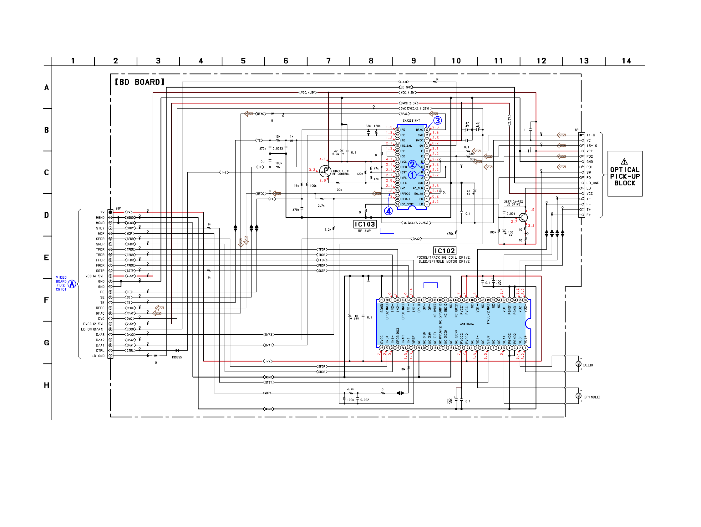
3-3. PRINTED WIRING BOARD — CD MECHANISM SECTION (1/2) — • Refer to page 19 for Circuit Boards Location.
A
B
C
D
E
F
1
234567891011 12 13 14
M101
C163
C182
C166
C164
C165
C153
R228
R125
R227
R126
C101
C102
R229
C104
C112
C109
C103
R117
C120
C111
C115
C108
C117
R113
R109
R103
R102
R105
R111
Q102
R118
R114
C110
R179
R176
R104
C107
R120
R112
IC103
Q101
D101
C213
R152
C151
R235
IC102
R151
R236
CN101
R231
(Page 24)
G
H
C188
C114
C119
R122
C113
R123
R124
C118
• Semiconductor
Location
Ref. No. Location
D101 D-9
IC102 B-11
IC103 E-9
Q101 F-8
Q102 C-8
R234
CN102
M102
2020
• Refer to page 19 for Waveforms.
3-4. SCHEMATIC DIAGRAM — CD MECHANISM SECTION (1/2) — • Refer to page 43 for IC Block Diagrams.
TP49
C213
R105
R102
(Page 26)
CN101
TP55
TP56
TP57
TP58
TP59
TP60
TP61
TP62
TP63
TP64
TP65
TP66
TP67
TP69
TP70
TP71
TP72
TP73
TP74
TP75
TP76
TP77
TP78
TP79
TP80
TP68
R234
D101
R236
R235
TP17
TP18
TP19
C102
TP21
C104C101
R103
R104
C103
R227
R113
R229
C115
C117
Q102
R109
C165
R111
R118
TP27
C107
C153
R120
R112
R114
R117
IC B/D
R179
IC103
R231
IC B/D
TP24
C110
R228
R126
R125
C112
C109
TP23
C111
C108
IC102
C120
C166
R122
C182
C114
C113
Q101
R124
R123
C118
C119
TP22
TP26
TP25
TP54
TP16
TP53
TP52
TP15
TP14
HCD-RV20/RV50/RV60
CN102
TP51
TP50
TP13
M102
R152
R151
R176
C151
21 21
TP100
C163
C164
M101
HCD-RV20/RV50/RV60
3-5. PRINTED WIRING BOARDS — CD MECHANISM SECTION (2/2) — • Refer to page 19 for Circuit Boards Location.
A
B
C
D
1
234567891011 12 13 14 15
CN704
CN703
C751
R702
C737
C736
C735
R723
R722
R721
D701
R701
JW710
D711
C741
R713
CN702
R735
JW709
R734
JW708
R732
JW711
R733
JW707
JW706
JW705
CN705
Q731
R751
C752
JW712
CN741
CN742
C715
E
F
G
H
• Semiconductor
Location
Ref. No. Location
D701 D-6
D711 D-7
IC701 F-6
IC712 F-7
IC731 E-11
Q731 C-9
CN721
JW713
JW714
IC701
R711
R712
JW701
IC712
JW704
JW703
JW702
R731
C731
CN701
(Page 28)
IC731
CN731
CN751
S751
2222
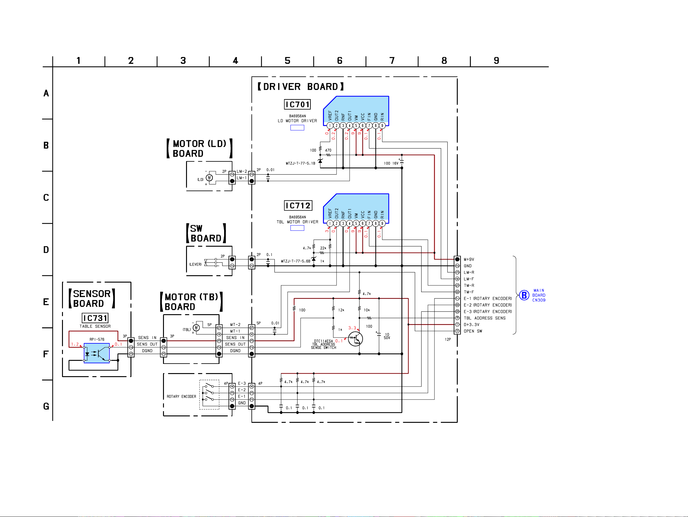
3-6. SCHEMATIC DIAGRAM — CD MECHANISM SECTION (2/2) — • Refer to page 44 for IC Block Diagrams.
IC701
IC B/D
R701
R702
HCD-RV20/RV50/RV60
IC731
CN731 CN741
M741
S751
M751
CN742
CN721
CN751
CN704
C751
C752CN705
D701
IC712
C715
IC B/D
R713
R712
R711D711
R751
R735
C741CN702
R733
Q731
R732R734
R731
C731
CN701
(Page 31)
RE701
CN751
CN703
R723 R721R722
C735C736C737
23 23
 Loading...