

Page 1

PRODUCTION SWITCHER
DFS-800
4 DIGITAL VIDEO INPUT BOARD
BKDF-810
2 ANALOG VIDEO INPUT BOARD
BKDF-811
16 INPUT DME BOARD
BKDF-840
4 DIGITAL VIDEO OUTPUT BOARD
BKDF-860
2 ANALOG VIDEO OUTPUT BOARD
BKDF-861
SERVICE MANUAL
1st Edition
Page 2

! WARNING
This manual is intended for qualified service personnel only.
To reduce the risk of electric shock, fire or injury, do not perform any servicing other than that
contained in the operating instructions unless you are qualified to do so. Refer all servicing to
qualified service personnel.
! WARNUNG
Die Anleitung ist nur für qualifiziertes Fachpersonal bestimmt.
Alle Wartungsarbeiten dürfen nur von qualifiziertem Fachpersonal ausgeführt werden. Um die
Gefahr eines elektrischen Schlages, Feuergefahr und Verletzungen zu vermeiden, sind bei
Wartungsarbeiten strikt die Angaben in der Anleitung zu befolgen. Andere als die angegeben
Wartungsarbeiten dürfen nur von Personen ausgeführt werden, die eine spezielle Befähigung
dazu besitzen.
! AVERTISSEMENT
Ce manual est destiné uniquement aux personnes compétentes en charge de l’entretien. Afin
de réduire les risques de décharge électrique, d’incendie ou de blessure n’effectuer que les
réparations indiquées dans le mode d’emploi à moins d’être qualifié pour en effectuer d’autres.
Pour toute réparation faire appel à une personne compétente uniquement.
Attention-when the product is installed in Rack:
1. Prevention against overloading of branch circuit
When this product is installed in a rack and is
supplied power from an outlet on the rack, please
make sure that the rack does not overload the supply
circuit.
2. Providing protective earth
When this product is installed in a rack and is
supplied power from an outlet on the rack, please
confirm that the outlet is provided with a suitable
protective earth connection.
3. Internal air ambient temperature of the rack
When this product is installed in a rack, please make
sure that the internal air ambient temperature of the
rack is within the specified limit of this product.
For safety, do not connect the connector for peripheral
device wiring that might have excessive voltage to the
following port.
: TO CP connector
: TO MU connector
Follow the instructions for the above port.
4. Prevention against achieving hazardous
condition due to uneven mechanical loading
When this product is installed in a rack, please make
sure that the rack does not achieve hazardous
condition due to uneven mechanical loading.
5. Install the equipment while taking the operating
temperature of the equipment into consideration
For the operating temperature of the equipment, refer
to the specifications of the Operation Manual.
6. When performing the installation, keep the
following space away from walls in order to
obtain proper exhaust and radiation of heat.
Front, Left : 10 cm (4 inches) or more
DFS-800
Page 3
CAUTION
Danger of explosion if battery is incorrectly replaced.
ADVARSEL!
Lithiumbatteri-Eksplosionsfare ved fejlagtig
håndtering.
Udskiftning må kun ske med batteri
af samme fabrikat og type.
Levér det brugte batteri tilbage til leverandøren.
ADVARSEL
Replace only with the same or equivalent type
recommended by the manufacturer.
Dispose of used batteries according to the
manufacturer’s instructions.
Vorsicht!
Explosionsgefahr bei unsachgemäßem Austausch
der Batterie.
Ersatz nur durch denselben oder einen vom
Hersteller empfohlenen ähnlichen Typ. Entsorgung
gebrauchter Batterien nach Angaben des
Herstellers.
ATTENTION
Il y a danger d’explosion s’il y a remplacement
incorrect de la batterie.
Remplacer uniquement avec une batterie du même
type ou d’un type équivalent recommandé par le
constructeur.
Mettre au rebut les batteries usagées conformément
aux instructions du fabricant.
Lithiumbatteri - Eksplosjonsfare.
Ved utskifting benyttes kun batteri som
anbefalt av apparatfabrikanten.
Brukt batteri returneres
apparatleverandøren.
VARNING
Explosionsfara vid felaktigt batteribyte.
Använd samma batterityp eller en likvärdig typ
som rekommenderas av apparattillverkaren.
Kassera använt batteri enligt gällande
föreskrifter.
VAROITUS
Paristo voi räjähtää jos se on virheellisesti
asennettu.
Vaihda paristo ainoastaan laitevalmistajan
suosittelemaan tyyppiin.
Hävitä käytetty paristo valmistajan ohjeiden
mukaisesti.
DFS-800
1 (P)
Page 4

Page 5

Index
Before turning off the power.........................................................................................................................1
1. Specification and Apperance.....................................................................................................................2
1-1. Specification ......................................................................................................................................2
1-1-1. DFS-800 Processor.....................................................................................................................2
1-1-2. DFS-800 Control Panel..............................................................................................................3
1-1-3. BKDF-810..................................................................................................................................4
1-1-4. BKDF-811..................................................................................................................................4
1-1-5. BKDF-860..................................................................................................................................4
1-1-6. BKDF-861..................................................................................................................................5
1-2. Appearance.........................................................................................................................................6
1-2-1. DFS-800 Processor.....................................................................................................................6
1-2-2. DFS-800 Control Panel..............................................................................................................7
2. Name and Function of Each Block............................................................................................................8
2-1. DFS-800 Processor ............................................................................................................................8
2-2. DFS-800 Control Panel......................................................................................................................9
2-2-1. Control Panel..............................................................................................................................9
2-2-2. Rear Panel ................................................................................................................................10
2-3. Peripheral Interface..........................................................................................................................11
2-4. DFS-800 Board Configuration.........................................................................................................14
3. Connection...............................................................................................................................................15
3-1. Basic Configuration......................................................................................................................... 15
3-2. Option Configuration.......................................................................................................................16
4. Function Block Diagram of Each Board .................................................................................................17
4-1. Function Block Diagram of CPU Board..........................................................................................17
4-2. Function Block Diagram of MAIN Board.......................................................................................18
4-3. Function Block Diagram of GENLOCK Board...............................................................................19
4-4. Function Block Diagram of BKDF-810 Board................................................................................20
4-5. Function Block Diagram of BKDF-811 Board................................................................................21
4-6. Function Block Diagram of BKDF-840 Board................................................................................22
4-7. Function Block Diagram of BKDF-860 Board................................................................................23
4-8. Function Block Diagram of BKDF-861 Board................................................................................24
5. Adjustment Procedure of Each Board......................................................................................................25
5-1. Adjustment of CPU Board ...............................................................................................................25
5-2. Adjustment of MAIN Board ............................................................................................................27
5-3. Adjustment of GENLOCK Board....................................................................................................28
5-4. Adjustment of BKDF-810 Board.....................................................................................................29
5-5. Adjustment of BKDF-811 Board.....................................................................................................30
5-6. Adjustment of BKDF-840 Board.....................................................................................................31
Page 6

5-7. Adjustment of BKDF-860 Board .....................................................................................................32
5-8. Adjustment of BKDF-861 Board .....................................................................................................32
6. Method of Board Replacement/Addition.................................................................................................33
6-1. Removal/Installation of Shield Plate................................................................................................33
6-1-1. Removal of Shield Plate...........................................................................................................33
6-1-2. Installation of Shield Plate........................................................................................................34
6-1-3. Caution on Insertion of Shield Plate.........................................................................................35
6-2. Replacement of CPU Board.............................................................................................................36
6-2-1. Removal of CPU Board............................................................................................................36
6-2-2. Installation of CPU Board........................................................................................................37
6-2-3. Setting.......................................................................................................................................37
6-3. Replacement of MAIN Board..........................................................................................................38
6-3-1. Removal of MAIN Board.........................................................................................................38
6-3-2. Installation of MAIN Board .....................................................................................................39
6-4. Replacement of GENLOCK Board..................................................................................................40
6-4-1. Removal of GENLOCK Board.................................................................................................40
6-4-2. Installation of GENLOCK Board.............................................................................................41
6-5. Replacement/Addition of BKDF-810 Board....................................................................................42
6-5-1. To Begin with...........................................................................................................................42
6-5-2. Removal of BKDF-810 Board..................................................................................................43
6-5-3. Installation of BKDF-810 Board..............................................................................................44
6-5-4. Setting and Confirmation of Operation....................................................................................45
6-6. Replacement/Addition of BKDF-811 ..............................................................................................46
6-6-1. To Begin with...........................................................................................................................46
6-6-2. Removal of BKDF-811 Board..................................................................................................47
6-6-3. Installation of BKDF-811 Board ..............................................................................................48
6-6-4. Setting and Confirmation of Operation....................................................................................49
6-7. Replacement/Addition of BKDF-840 ..............................................................................................50
6-7-1. Removal of BKDF-840 Board..................................................................................................50
6-7-2. Installation of BKDF-840 Board..............................................................................................51
6-7-3. Setting and Confirmation of Operation....................................................................................52
6-7-4. Positioning Drawing for affixing the rubber ............................................................................52
6-8. Replacement/Addition of BKDF-860 Board....................................................................................53
6-8-1. To Begin with...........................................................................................................................53
6-8-2. Removal of BKDF-860 Board..................................................................................................54
6-8-3. Installation of BKDF-860 Board..............................................................................................55
6-8-4. Confirmation of Operation.......................................................................................................55
6-9. Replacement/Addition of BKDF-861 Board....................................................................................56
6-9-1. To Begin with...........................................................................................................................56
6-9-2. Removal of BKDF-861 Board..................................................................................................57
6-9-3. Installation of BKDF-861 Board..............................................................................................58
6-9-4. Confirmation of Operation.......................................................................................................59
Page 7

7. Update of Firmware/Software.................................................................................................................60
7-1. Procedure of Version Confirmation .................................................................................................60
7-1-1. Confirmation of GUI Version...................................................................................................60
7-1-2. Confirmation of CPU1 Version................................................................................................60
7-2. Update Procedure.............................................................................................................................61
7-3. Update of GUI Software..................................................................................................................62
7-4. Update of Board Firmware ..............................................................................................................62
8. FAQ・Troubleshooting...........................................................................................................................63
8-1. Trouble at Startup.............................................................................................................................63
8-2. Trouble related to Input and Output.................................................................................................64
8-3. Trouble after Board Addition/Replacement.....................................................................................65
8-4. Trouble related to Updating.............................................................................................................65
8-5. Trouble related to Function..............................................................................................................66
9. Error Code Table .....................................................................................................................................67
10. Replacement Parts for Mainteance........................................................................................................68
10-1. List of Replacement Parts for Maintenance ...................................................................................68
10-2. Replacement of DFS-800 Processor Parts.....................................................................................69
10-2-1. Removal of Front Panel.......................................................................................................... 69
10-2-2. Removal of Top Cover ...........................................................................................................69
10-2-3. Replacement of Power Unit ...................................................................................................70
10-2-4. Replacement of Fan................................................................................................................74
10-3. Replacement of DFS-800 Control Panel Parts...............................................................................77
10-3-1. Removal of Control Panel......................................................................................................77
10-3-2. Replacement of Power Supply...............................................................................................78
10-3-3. Replacement of Flash Memory ..............................................................................................80
10-3-4. Replacement of Button Cell...................................................................................................81
Page 8

Page 9
Before turning off the power
Before turning off the DFS-800 Processor, shut down in the manner below.
1) Confirm that the USB is not accessed.
2) Press the F1 knob and F4 knob simultaneously. Then, the display on the panel changes as shown
below.
Shutdown?
3) Press the F2 knob. ( To cancel the shutdow, press the F3 knob.)
4) When the F2 knpb is pressed, the shutdown begins. When the DFS-800 Processor is normally
shut down, the display on the panel changes as shown below.
Shutdown…OK!
5) Turn off the power of Control Panel and then the power of Processor.
F2: OK F3: CANCEL
Caution
Before turning off the power, be sure to shut down. If the power is turned off before
shut-down, the present panel setting cannot be saved. Therefore, the system is not
normally terminated and the re-startup may fail.
When the system is normally shut down, the previous panel setting can be restored at
the startup.
1
Page 10

1. Specification and Apperance
1-1. Specification
1-1-1. DFS-800 Processor
Television System 525/60, 625/50
Signal Process Method Digital Component 4:2:2 4 ( key ) 10 bits
Quantization Y: 10 bits, C: 10 bits, Key: 10 bits
Video Input SD SDI 270Mpbs, 75Ω, 8 inputs ( Expandable up to 16 inputs ), BNC
Sync Signal Input BB: 0.429 Vp-p ( NTSC ) or 0.45 Vp-p ( PAL ),
75Ω or loop-through, 1 input, BNC
Video Output SD SDI 270Mpbs, 75Ω, 8 outputs ( Program 2 outputs, Preview,
Clean 1 output each , Auxiliary 4 outputs ) ( Expandable up to 16 outputs ),
BNC
Sync Signal Output BB: 0.429 Vp-p ( NTSC ) or 0.45 Vp-p ( PAL ), 75Ω, 2 utputs, BNC
I/O Delay 1H (minimum delay) – 4 frames
Interface
TO OU
( To control panel ):
RS-422: D-sub 9-pin ( female ), 2 ports
EDITOR D-sub 9-pin ( female ), 1 port
REMOTE: D-sub 37-pin ( female ), 1 port ( 8-pin input/24-pin output )
Operating Temperture 5°C - 40°C
Operating Humidity 30% - 90% ( No dropwise )
Power Source 100VAC-240VAC, 50/60Hz
Current Consumption 1.9A - 0.9A
Maximun In-rush
Current
Weight About 15kg
Dimensions 430 ( W ) x 425( D ) x 88 ( H ) mm, EIA 2RU
Ethernet, 10/100BASE-TX, RJ-45; 1 port
(1) Power ON, current probe method: 60A ( 240V )
(2) Hot switching inrush current, measured in accordance with European
standard EN55103-1: 20A ( 230V )
Consumed Parts Cooling Fan: x1 at front side Replacement: every 4 years
x2 at rear side Replacement: every 4 years
2
Page 11

1-1-2. DFS-800 Control Panel
USB
( Control Panel )
Interface
TO PANEL D-sub 9-pin ( female ), 1 port
TO MU (To switcher) Ethernet 10/100BASE-TX, RJ-45, 1 port
VGA VGA OUT, D-sub 15-pin ( female )
USB: USB1.1, A type ( female ), 1 port
Operating Temperature 5°C - 40°C
Operating Humidity 30% - 90% ( No dropwise )
Power Source 100VAC-240VAC, 50/60Hz
Current Consumption 0.5A - 0.2A
Maximum In-rush
Current
Weight About 5kg
USB1.1, A type ( female ), 1 port
For USB memory stick ( Up to 2GB ).
(1) Power ON, current probe method: 40A ( 240V )
(2) Hot switching inrush current, measured in accordance with European
standard EN55103-1: 10A ( 230V )
Dimenstions 430 ( W ) x 221 ( D ) x 117 ( H ) mm
3
Page 12

1-1-3. BKDF-810
Television System 525/60, 625/50
Video Input SD SDI 270Mpbs, 75Ω, 4 inputs, BNC
I/O Delay 1 Frame ( When FS is used )
1-1-4. BKDF-811
Television System 525/60, 625/50
Video Input Analog Composite 2 inputs or
Analog Composite and Analog Component 1 input each
Analog Composite: 1.0V ( p-p ) 75Ω BNC
Analog Component
Y: 1.0V ( p-p ) 75Ω BNC
B-Y, R-Y: 0.486V ( p-p ) ( SMPTE Level, 7.5% Setup )
0.525V ( p-p ) ( SMPTE Level, 0% Setup )
0.700V ( p-p ) ( Betacam Level, 7.5% Setup )
0.757V ( p-p ) ( Betacam Level, 0% Setup )
Phase Control ±8 Pixcels
I/O Delay 1 Frame ( The FS is always turned on. )
1-1-5. BKDF-860
Television System 525/60, 625/50
Video Input SD SDI 270Mpbs, 75Ω, 4 outputs, BNC
4
Page 13

1-1-6. BKDF-861
Television System 525/60, 625/50
Video Output Analog Composite 2 outputs or
Analog Composite and Analog Component 1 output each
Analog Composite: 1.0V ( p-p ) 75Ω BNC
Analog Component Y,B-Y,R-Y
Y: 1.0V ( p-p ) 75Ω BNC
B-Y, R-Y: 0.486V ( p-p ) ( SMPTE Level, 7.5% Setup )
0.525V ( p-p ) ( SMPTE Level, 0% Setup )
0.700V ( p-p ) ( Betacam Level, 7.5% Setup )
0.757V ( p-p ) ( Betacam Level, 0% Setup )
Analog Component GBR
G, B, R: 1.0V ( p-p ) 75Ω BNC
Characterristics
At Analog Composite Output:
Frequency
Chatacteristics
S/N Ratio
DG/DP
K Factor
HV Tilt
Residual Jitter
At Analog Component Y,B-Y,R-Y output:
Frequency
Characteristics
S/N Ratio
Linearity
K Factor
Phase difference
between Y/B-Y/R-Y
100kHz - 4.2MHz: ±0.5dB,
4.2MHz - 5MHz: within -1dB,
Over 5MHz: Descending characteristics
60dB ( Excluding quantizing noise )
1%/1°
1%
1%
±15ns
100kHz - 4.2MHz: ±0.5dB,
4.2MHz - 5MHz: within -1dB,
Over 5MHz: Descending characteristics
60dB ( Excluding quantizing noise )
2%
1%
10ns
At nalog Component GBR output:
Frequency
Chatacteristics
S/N Ratio
K Factor
100kHz - 5MHz: ±0.5dB,
Over 5MHz: Descending characteristics
60dB ( Excluding quantizing noise )
1%
5
Page 14
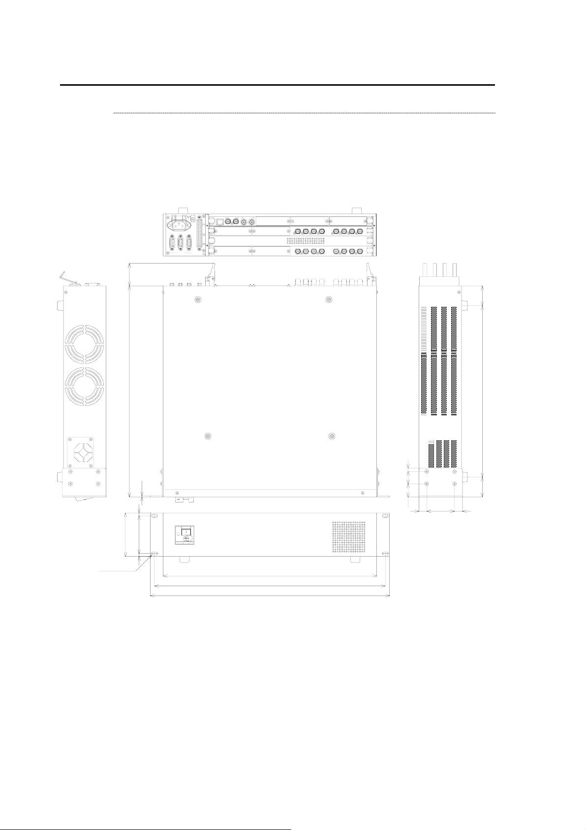
1-2. Appearance
1-2-1. DFS-800 Processor
( In mm. )
U
O
T
B
B
I
K
N
C
O
L
O
U
4
I
N
z
H
/
0
0
5
6
V
0
4
O
T
R
I
D
E
2
2
2
4
-
S
45
4
2
-
0
0
1
C
A
3
3
2
2
1
R
E
T
M
O
E
R
1
1
N
O
E
T
G
1
2
8
7
6
5
4
X
4
U
A
3
U
X
A
X
2
U
A
X
U
1
A
N
A
E
L
C
V
I
D
E
O
I
N
3
2
1
V
I
D
T
E
O
U
O
V
E
R
P
2
M
G
P
1
M
G
P
425
2x2-6.4x12
t2.3
26.5 24.5 7
DFS-800
PRODUCTION SWITCHE R
88
ON
OFF
16 56 16
6766
430
465
482
40 345 40
6
Page 15
1-2-2. DFS-800 Control Panel
( In mm. )
7
Page 16
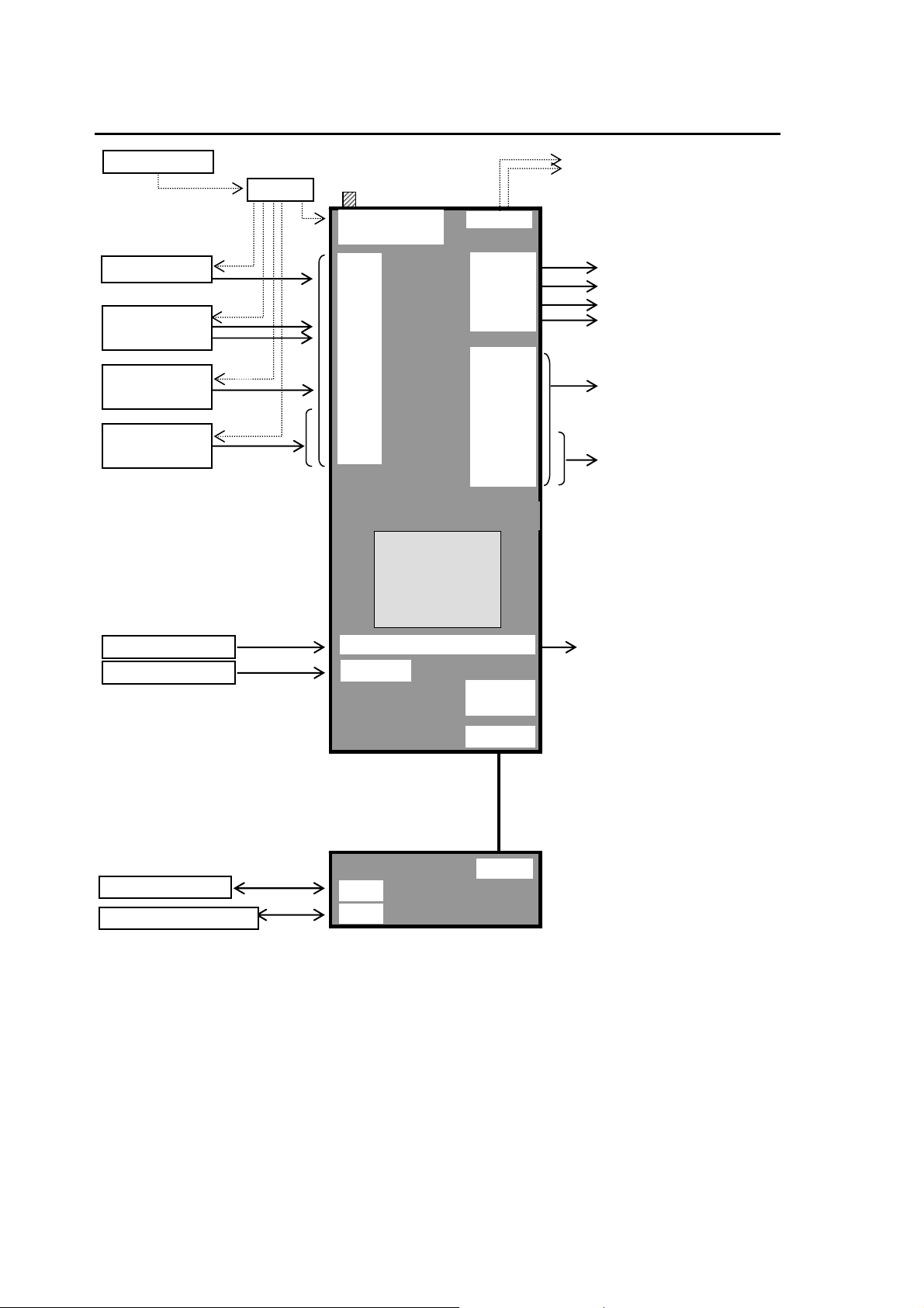
2. Name and Function of Each Block
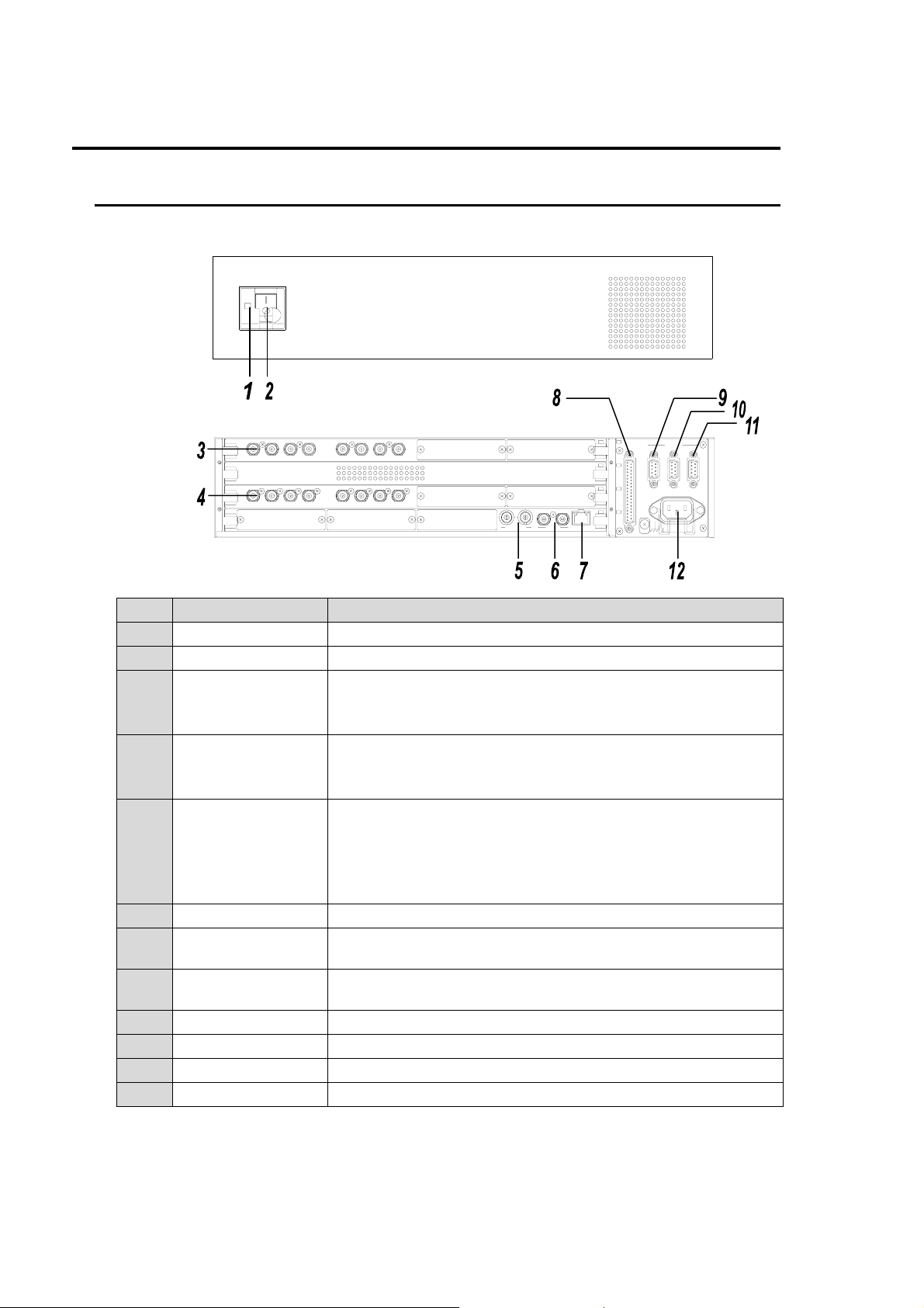
2-1. DFS-800 Processor
Front Panel
Rear Panel
No. Name Function
1 POWER LAMP When turning on the power, the POWER lamp lights green.
2 POWER SWITCH Power switch of DFS-800
3 VIDEO OUT
4 VIDEO INPUT
5 GENLOCK IN
6 REF OUT Connector for sync signal output 2 outputs
7 TO CP
8 REMOTE
9 RS-422 -1 Connector for RS-422 control D-sub 9-pin ( female )
10 RS-422 -2 Connector for RS-422 control D-sub 9-pin ( female )
11 RS-422 - EDITOR Connector for editor control D-sub 9-pin ( female )
12 AC IN For power input Feed AC100V - 240V.
ON
OFF
E
R
E
X
U
A
P
V
2
1
G
P
M
V
I
D
E
O
O
U
T
1
V
I
D
E
O
I
N
L
C
A
N
M
G
P
3
4
2
X
U
A
1
2
A
A
U
3
X
U
4
X
7
5
8
6
2
1
N
T
K
C
N
B
E
O
B
G
I
O
L
U
SD SDI Digital Video output
2 programs, 1 preview, 1 clean and 4 auxiliaries are provided for
standard output. 8 auxiliary outputs can be added.
SD SDI Digital Video output
8 inputs are provided for standard input. 8 inputs can be added as
an option.
Connector for inputting the external sync signal ( black burst )
When a signal is fed to one connector, the other connector becomes
automatically the loop through connector.
When desiring no loop through, terminate the other connector with
75Ω.
Connector for connecting the Control Panel ( RJ-45,
10Base-T/100Base-TX ).
Connector for inputting GPI, connector for outputting GPI/Tally
D-sub 37-pin ( female )
DFS-800
PRODUCTION SWITCHER
1
1
E
O
M
T
E
R
S
R
4
2
2
E
I
D
1
T
R
O
2
2
2
3
3
4
4
U
O
T
O
I
z
N
0
H
V
/
A
6
0
0
0
-
C
5
1
2
4
0
8
Page 17
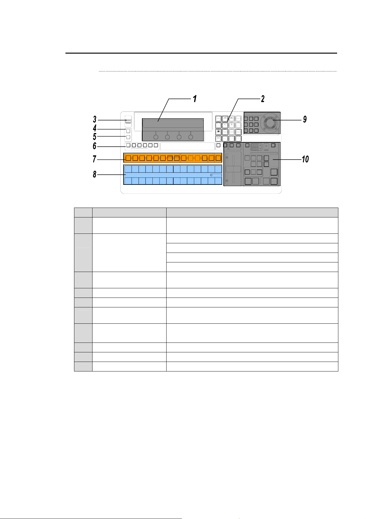
2-2. DFS-800 Control Panel
2-2-1. Control Panel
The configuration of each part of control panel is as follows.
PROGRAM
PRESET
USB MEMORY
BLACK
BLACK
EDITOR
GPI
KEY ON
KEY1
MATTE
EXT SELF CK EDGE SHADOWMASK
KEYER
BUS SELECT
KEY3
KEY2
INPUT SYSTEM
AUX
2
1
2
1
F3 F4F2F1
PRODUCTION SWITCHER
DME
BORDERBASIC
COMB B
COMB A
DSK2
DSK1
KEY4
STATUS
SETUP
443
3
EVENT
SEQ
STILL
7
6
5
7
6
5
SUB EFF
8
10109
8
9
No. Name Function
Display panel and menu
1
control
2 digits display panel for menu and control knpb for menu
setting
Operation mode select button of menu, event and sequence
2 Keypad and mode button
Used for input/change of menu.
Used for save/call of event.
Used for save/replay of sequence.
3 USB Memory
Used for save/read of data. ( exclusive for USB flash memory,
up to 2GB, USB 1.1 or 2.0 )
4 EDITOR button Used for ON/OFF editor control.
5 GPI button Used for ON/OFF of GPI IN control.
6 Keyer section
Used for keyer setup. ( Settings of keyer signal, type
selection,mask, edge and shadow )
WARP LIGHT
11
MENU
SEQ
4
1
SEQ LINK
SHIFT
SHIFT
121211
COMBINER SETU P
SHIFT
8 97
65
RECALL
LOOP DIR
23
INSERT
DELETE
NEW
CANCEL
.0
FADER LIMIT NOR/REV REVERSE PREV TRANS
FADER DIRECTION
EVENT
FINE
X
DEFAULT
STORE
WIPE POSAUTO CK
Y
Z
DME POS DME ROT
JOYSTICK
DFS-800
CUT
1
WIPE
(FAM)
TRANSITION TYPE
PRODUCTION SWITCHER
HIGH
321
2434
1 OVER 2
PRIOR ITY
4321
21
LOW1 234
KEY LAYER
DSK
KEY STATUS
DSK
KEY
KEY
1
2
1
DSK
KEY
KEY
2
4
3
DME
BLACK
TRANS
(NAM)
DSK
TRANSITION
DSK
CUT
MIX
AUTO
ENTER
BKGD
MIX
BUS SELECT、SETUP、
7
DME section
Selects a bus and displays menu.
8 M/E bus Selects the background video.
9 Joystick block Used for menu operation and auto chroma key setting.
10 Transition block Executes the transitions of background and key.
9
Page 18
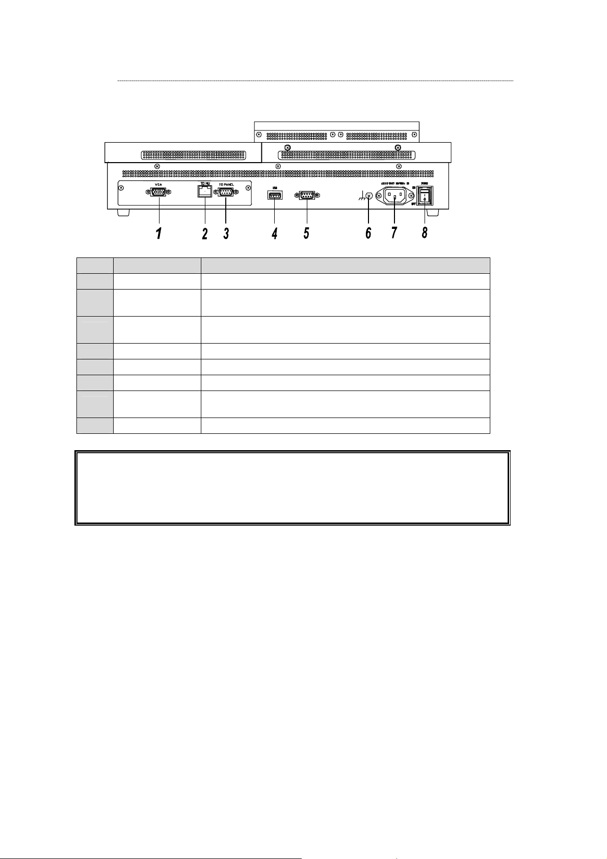
2-2-2. Rear Panel
The configuration of rear panel of control panel is as follows.
No. Name Function
1 VGA Cconnect the LCD monitor.
2 TO MU
3 TO PANEL
4 USB Connect the USB flash memory. ( Up to 2GB, USB 1.1 or 2.0 )
5 ― Not used
6 Ground For safety, connect it to the ground.
7 AC IN
8 Power Switch Power switch of control panel
Connect the Processor. ( RJ-45, 10Base-T/100Base-TX,
category5, cross cable )
Connect the touch panel LCD.
( RS232C, D-sub 9-pin (female ) )
Using the supplied power cord, supply the AC power.
( AC100V-240V 50/60Hz ).
Caution
The USB port is exclusively for connecting the mouse or USB flash memory. Other
USB drive equipment cannot be recognized. Insert the USB memory stick either in
the USB memory drive on the control panel or USB memory drive on the rear panel.
Do not insert in both of them at the same time.
10
Page 19
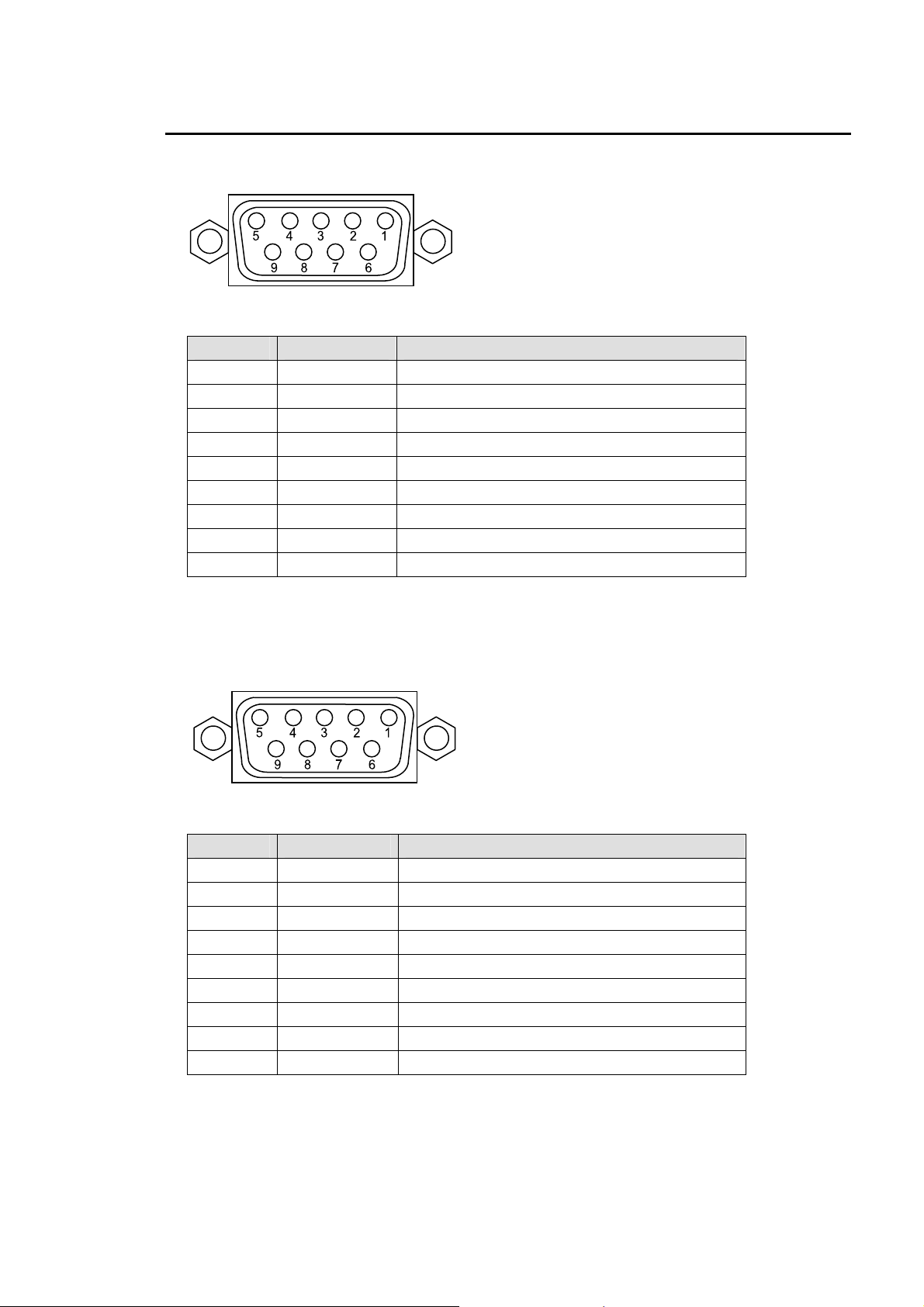
2-3. Peripheral Interface
EDITOR CONNECTOR
Pin Assignment Table ( D-sub 9-pin, female )
Pin No. Signal Name Content
1 FG Frame Ground
2 T- Data Send ( - )
3 R+ Data Receive ( + )
4 SG Signal Ground
5 - Not used
6 SG Signal Ground
7 T+ Data Send ( + )
8 R- Data Receive ( - )
9 FG Frame Ground
Cable Connector: D-sub 9-pin connector ( male ), Inch screws are used.
RS-422 (1) (2) Connector
Pin Assignment Table ( D-sub 9-pin, female )
Pin No. Signal Name Content
1 FG Frame Ground
2 R- Data Receive ( - )
3 T+ Data Send ( + )
4 SG Signal Ground
5 - Not used
6 SG Signal Ground
7 R+ Data Receive ( + )
8 T- Data Send ( - )
9 FG Frame Ground
Cable Connector: D-sub 9-pin connector ( male ), Inch screws are used.
11
Page 20
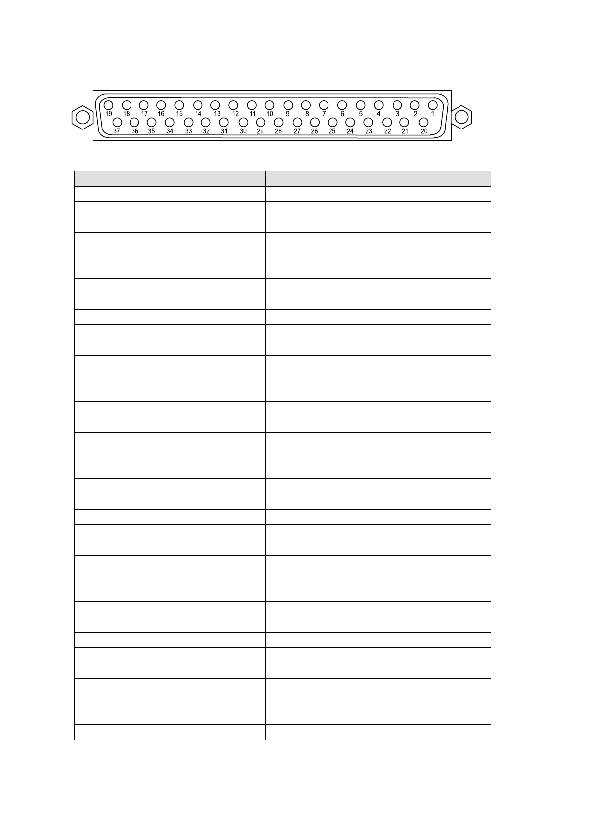
REMOTE Connector
Pin Assignment Table ( D-sub 37-pin, female )
Pin No. Pin Function Default Setting
1 Tally Output 1 RedTallyInput01
2 Tally Output 2 RedTallyInput02
3 Tally Output 3 RedTallyInput03
4 Tally Output 4 RedTallyInput04
5 Tally Output 5 RedTallyInput05
6 Tally Output 6 RedTallyInput06
7 Tally Output 7 RedTallyInput07
8 Tally Output 8 RedTallyInput08
9 Tally Output 9 GreenTallyInput01
10 Tally Output 10 GreenTallyInput02
11 Tally Output 11 GreenTallyInput03
12 Tally Output 12 GreenTallyInput04
13 Tally Output 13 GreenTallyInput05
14 Tally Output 14 GreenTallyInput06
15 Tally Output 15 GreenTallyInput07
16 Tally Output 16 GreenTallyInput08
17 +5V
18 +5V
19 +5V
20 Tally Output 17 None
21 Tally Output 18 None
22 Tally Output 19 None
23 Tally Output 20 None
24 Tally Output 21 None
25 Tally Output 22 None
26 Tally Output 23 None
27 Tally Output 24 None
28-29 GND
30 GPI 1 PGMAutoTrans
31 GPI 2 PGMCutTrans
32 GPI 3 DSKAutoTrans< Mix >
33 GPI 4 DSKCutTrans
34 GPI 5 PGMMixType
35 GPI 6 PGMWipeType
36 GPI 7 PGMDMEType
37 GPI 8 BlackTrans
12
Page 21
Cable Connector
D-sub 37-pin ( male ), Inch screws are used. Maximum load current DC 0.1A
Pin Free assignment
The table shown on the previous page shows the setting of pin assignment at ex-factory. They
can be changed on the menu.
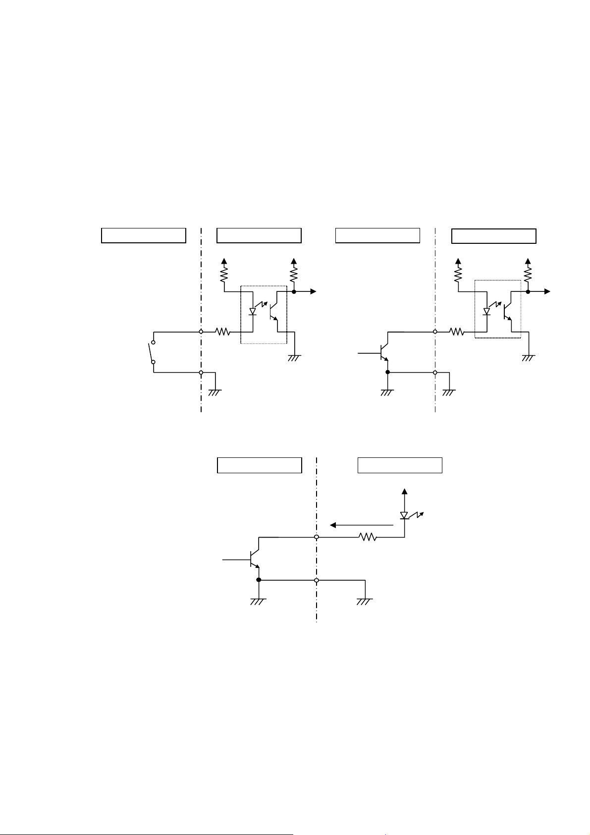
GPI Input Circuit
Switch or Relay
External Equipment
Tally Output Circuit
DFS-800
DFS-800
Open Collector
External Equipment
VCCVCC
External Equipment
Maximum voltage:
30V
Maximum load
current
100mA
DFS-800
VCCVCC
13
Page 22
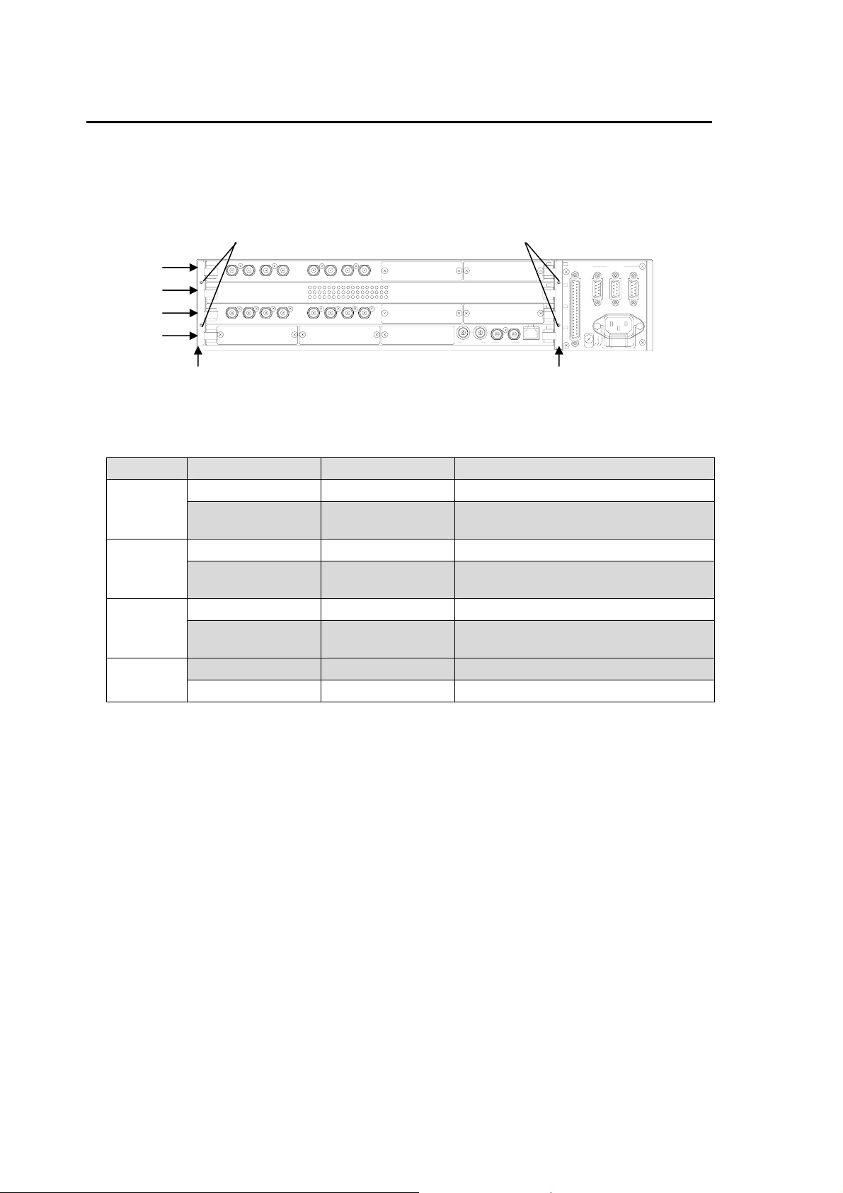
2-4. DFS-800 Board Configuration
r
w
The board configuration of DFS-800 rear panel is shown in the figure below and on the table. Each
board is fixed with the retainer. To draw out the board from the unit, remove the retainers and then
draw out the board.
1
2
3
4
Configuration of Rear Panel Card of DFS-800 (From top slot to down slot)
Slot Standard/Option Card Content
1
2
3
4
*1 For expansion of option input, refer to [ 6-5. Replacement/Addition of BKDF-810 board ]
and [ 6-6. Replacement/Addition of BKDF-811 board ]. For expansion of option output,
refer to [ 6-8. Replacement/Addition of BKDF-860 board ] and [ 6-9.
Replacement/Addition of BKDF-861 board ].
Screw Scre
M
P
V
2
1
M
G
P
G
P
E
V
I
D
E
O
O
U
V
I
D
E
O
I
N
R
T
3
1
2
U
A
L
C
A
N
E
7
5
4
8
6
2
1
T
N
U
B
B
I
O
K
C
O
L
N
E
G
1
1
E
R
O
M
T
2
2
3
3
4
4
U
O
T
O
4
X
A
U
X
U
A
3
X
U
1
2
A
X
Retainer Retaine
Standard BKDF-860 Standard SD-SDI 1-8 Output
Option
BKDF-860 /
BKDF-861
2 cards are expandable. ( *1 )
Standard MAIN MAIN card
Option BKDF-840
Input DME card
( Pre-combiner )
Standard BKDF-810 Standard SD-SDI 1-8 Input
Option
BKDF-810 /
BKDF-811
2 cards are expandable. ( *1 )
Option BKDF-811 2 cards are expandable. ( *1 )
Standard CPU CPU card
4
2
2
-
S
E
R
1
2
E
0
H
/
6
z
0
0
-
5
2
4
0
V
0
C
1
A
R
O
I
D
T
N
I
14
Page 23
3. Connection
(
)
3-1. Basic Configuration
TSG
VDA
Camera
Character
Generator
Digital Video
Database
GPI Controller
USB Flash Memory
(75ohm terminator)
GENLOCK IN
(w/ loop-through
IN 1
IN 2
IN 3
IN 4
IN 5
IN 6
IN 7
IN 8
REF OUT
REF OUT
CLEAN
DFS-800 Processor
30-37) REMOTE (1-27
EDITOR
RS-422 1
RS-422 2
TO OU
USB
TO MU
DFS-800 Control Panel
Reference outputs
PGM 1
PGM 2
PREV
AUX1
AUX2
AUX3
AUX4
Supplied LAN Cable
PGM1 output
PGM2 output
PREV output
CLEAN output
AUX outputs
(Free assign)
Tally outputs
Caution
Connect to the Control Panel with the supplied control cable (10m) or ( LAN
crosscable, category 5, RJ-45 ).
15
Page 24
3-2. Option Configuration
TSG
Camera
Character
Generator
Digital Video
Database
Analog Video
Database
GPI Controller
Editor, etc
SVGA Display
USB Flash Memory
VDA
(75ohm terminator)
GENLOCK IN
(w/ loop-through
IN 1
IN 2
IN 3
IN 4
IN 5
IN 6
IN 7
IN 8
IN 9
|
IN 16
DFS-800 Processor
(30-37) REMOTE (1-27)
EDITOR
Supplied LAN Cable
VGA
USB
REF OUT
BKDF-810
BKDF-811
BKDF-860
BKDF-861
BKDF-840
RS-422 1
RS-422 2
TO OU
DFS-800
PGM 1
REF OUT
PGM 2
PREV
CLEAN
AUX1
AUX2
AUX3
AUX4
AUX5
I
AUX12
TO MU
Reference outputs
PGM1 output
PGM2 output
PREV output
CLEAN output
AUX outputs
(SD-SDI)
AUX outputs
(Analog)
Tally outputs
16
Page 25
4. Function Block Diagram of Each Board
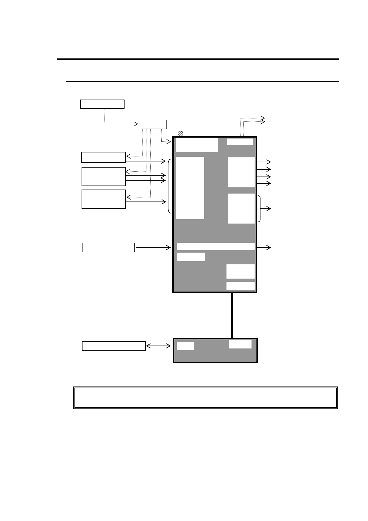
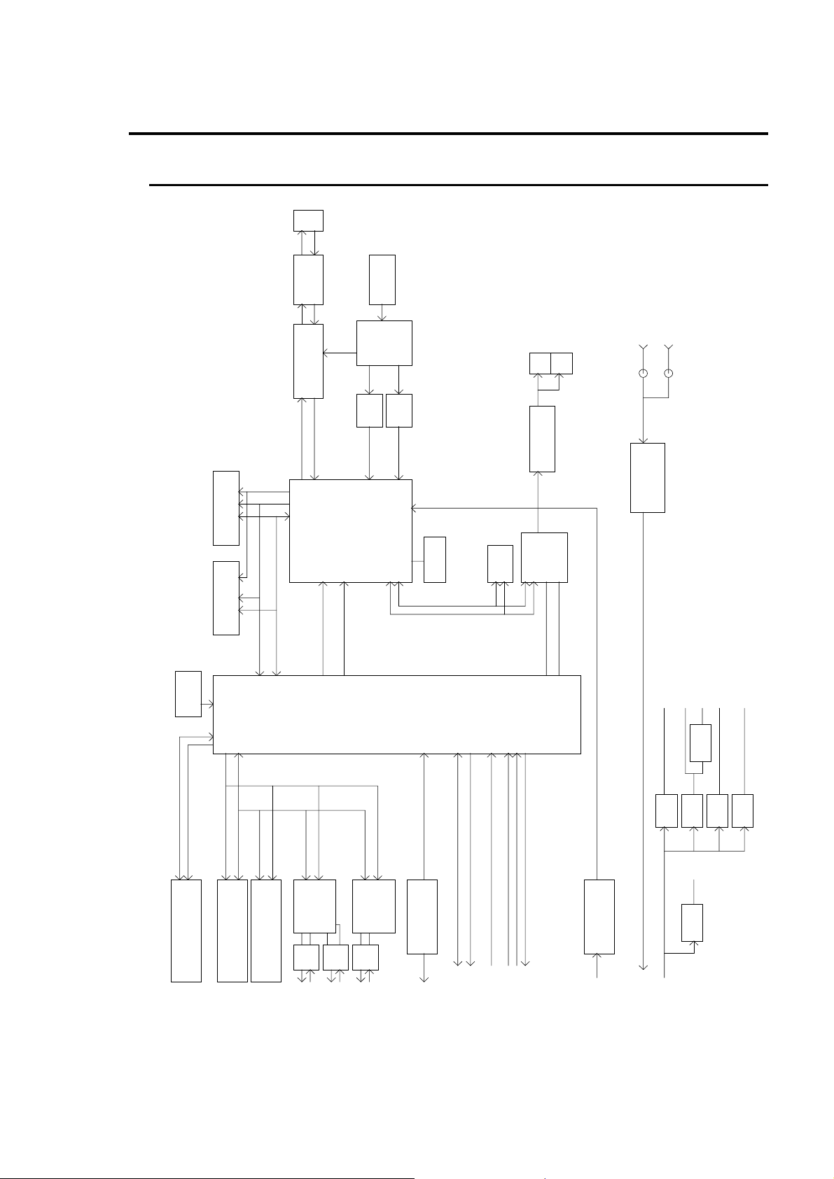
4-1. Function Block Diagram of CPU Board
SDRAM IC52
EDS1232AATA
133MHz
133MHz
Address Bus 22bits
SDRAM IC51
EDS1232AATA
133MHz
RJ45
IC30
PULSE TRANS
Ethernet Physical
IC29
M2 Interface TX
DATA Bus 64bits
BEL FUSE
25MHz
INTEL LXT971C
M2 Interface RX
DSP IC3
TMS320DM642
Crystal
Clock Buffer
25MHz
PLL
IC19
ICS511M
50MHz
IC18
TQC73DCP
IC21
IDT5V2310
25MHz
PLL
133MHz
I2C CLK
I2C DATA
IC19
ICS511M
JTAG I/F
DSP emulator
EEPROM
IC24
24LC16B
BB OUT
LEVEL & PEDESTAL
IC28,IC62,IC27
AD8091,AD8092
ENCODER
IC26
ADV7176A
CN1
BCJ-BPLH2P
75 Ohme COAX CABLE
CN8
BCJ-BPLH2P
CN9
BCJ-BPLH2P
Differential Signal
Driver
IC58,IC59
AD8132
75 Ohme COAX CABLE
ConfigROM
XCF02S-VOG20
I2C CLK
I2C DATA
Dangle CD
(I2C BUS EEPROM)
FPGA Xilinx
XC2S300E-7FG456C
IC33
Peripheral Data Bus 8bits
Peripheral Address Bus 26bits
Serial I/F
29LV128‚l
IC57
*NOT USED NOW
RS485
FLASH MEMORY
29LV128‚l
IC53
FLASH MEMORY
Multiplexed intrrupt signal
Video intrrupt signal
ADDRESS DECODER
I2C I/F
TARNSACTION BUS
Serial I/F
IC40
RS485
Driver
IC43
To Mother BD
Controller
RS485
Driver
Controller
TL16C752B
Driver
IC41
TL16C752B
IC45
IC44
24bits
GPO
IC38,IC38,IC39,IC42
ULN2003ANS
Transaction BUS 32bits
24bits
To Mother BD
ENC_BB 16bits
H SYNC/FELED/BLANKING
8bits
FAN ALARM 3bits
Frame Pulse from Genlock CD
POWER ALARM 1bit
Transaction BUS Device select (Each FPGA has a CS)
POWER LED CONTROL 2bits
To Mother BD
GPI
IC35,IC36
TLP280-4
8bits
From Mother BD
+3.3V
+2.5V
+1.4V
+5.0V
-5.0V
IC49
LP3965EMP
IC56
LM2660M
IC50
LT1764A
IC48
LP3966ES
IC46
LP3966ES
+1.8V
P1
Differential analog video signal go to the Genclock CD
To Mother BD
AXH005AOX
+5.25V
From Mother BD
17
Page 26
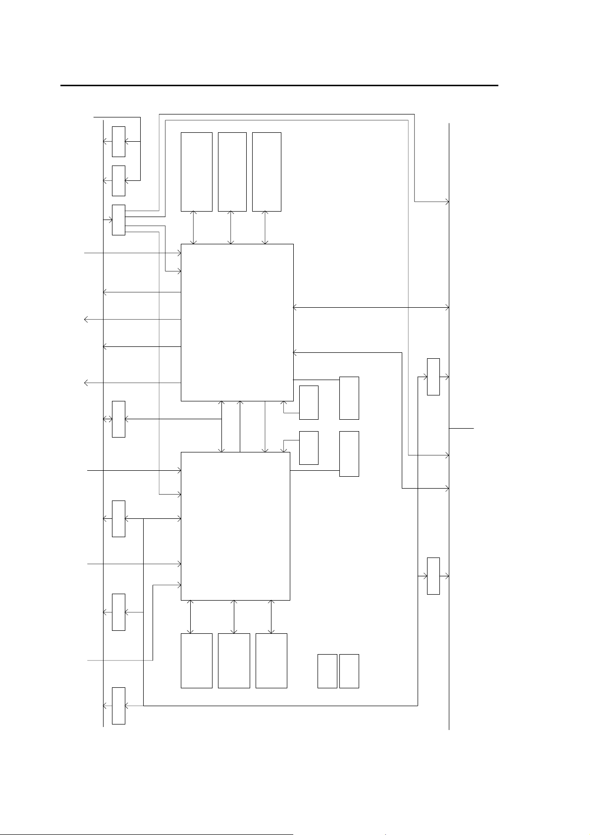
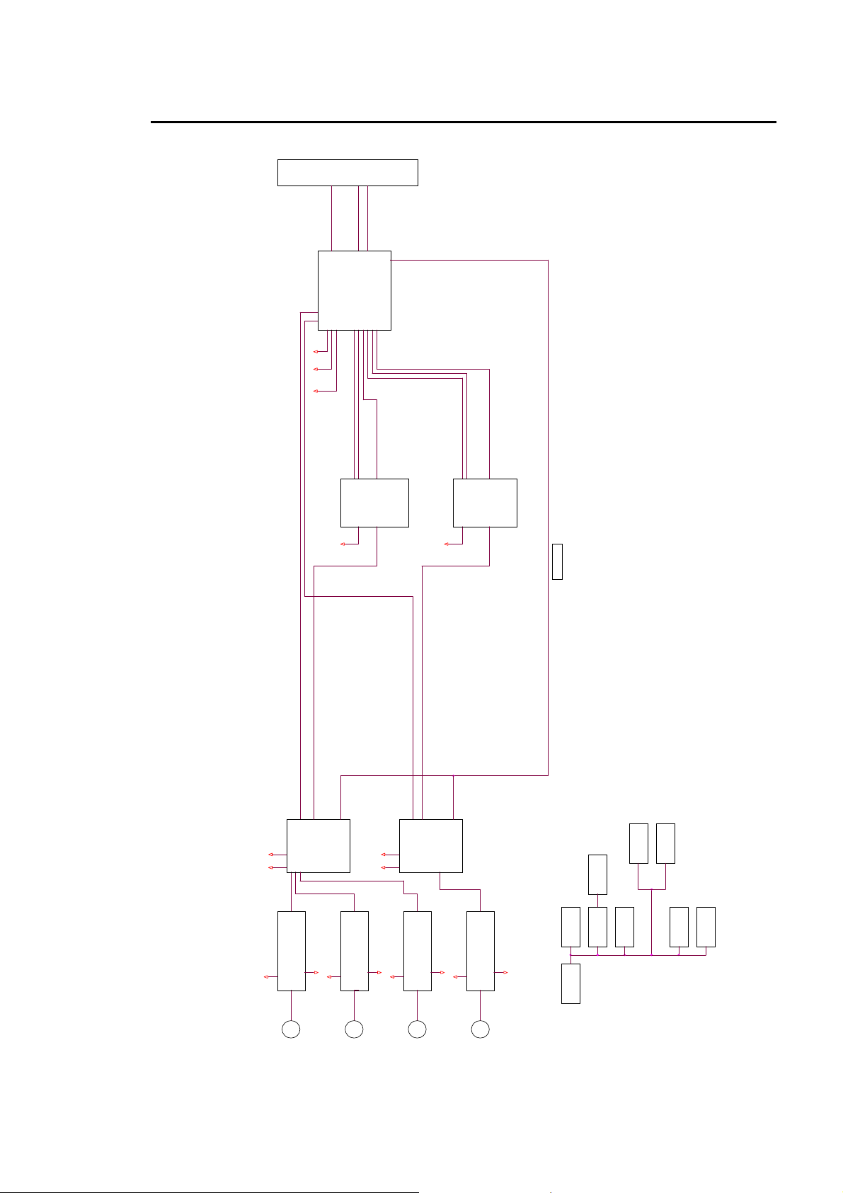
4-2. Function Block Diagram of MAIN Board
Transaction BUS
Clock IN 33MHz
To Mother Board
Pixel Clock 27MHz
From Genlock CD
VIDEO IN(Slot4)
LVDS 162MHz DDR
VIDEO OUT(Slot4)
VIDEO OUT(Slot3)
LVDS 162MHz DDR
VIDEO OUT(Slot2)
VIDEO OUT(Slot1)
LVDS 162MHz DDR
IC5IC7IC6
5V2310 5V2310 5V2310
LVDS 162MHz DDR
LVDS 162MHz DDR
IC15
IC18
Transaction BUS
Clock Distribution
33MHz
IC24
IC26
8ch Delay
IC25
PGM/PRV/DSK1/DSK2
KEY1/KEY2/KEY3/KEY4
Switcher Chip
M/E
KEYER
IC28
IC27
6ch Trail Store
DSK
IC29
INPUT DVE Filed Delay
Still Store
Caputure/Load
Key Delay for Edge
Chromakey
WIPE Generator
Mask Generator
Edge Generator
Still Store Controller
Trail
paint
Color Corrector
SDRAM Controller
P5P4
DC/DC
+5V to +1.5V
CORE POWER
MAIN CD(E02886-1)
Cofiguration ROMCofiguration ROM
IC43
IC44
LVC16245LVC16245
VIDEO IN/OUT
LVDS 162MHz DDR
*Write Only*
Transaction BUS
32bits 2.5V LVCMOS
Transaction BUS
32bits 2.5V LVCMOS
VIDEO IN(Slot3)
LVDS 162MHz DDR
IC14
*Write Only**Write Only**Write Only*
Transaction BUS
32bits 2.5V CMOS
VIDEO IN(Slot2)
LVDS 162MHz DDR
IC13
Transaction BUS
32bits 2.5V CMOS
VIDEO IN(Slot1)
LVDS 162MHz DDR
IC45
Transaction BUS
32bits 2.5V CMOS
IC17
LVC16245LVC16245
IC49
IC46
LVC16245 LVC16245
IC35
IC38
IC30 IC19
DVE ch1
DVE ch3
DVE Border
Warp Engin
Lighting
Effects Chip
IC36
IC39
DVE ch2
DVE ch5
IC37
IC40
DVE ch3
DVE ch6
DC/DC
+5V to +1.5V
CORE POWER
P2
DC/DC
+5V to +3.3V
I/O POWER
IC33 IC22
P3
DC/DC
+5V to +2.5V
I/O POWER
IC41
IC42
VIDEO IN/OUT
LVDS 162MHz DDR
DVE-SUB CD(E02882-1) DVE-SUB CD(E02882-1)
*Write Only*
Transaction BUS
32bits 2.5V LVCMOS
18
Page 27
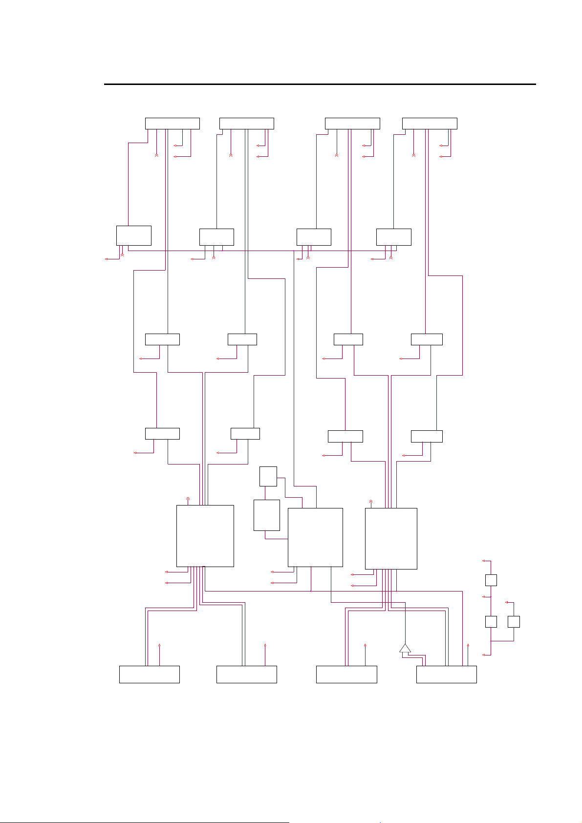
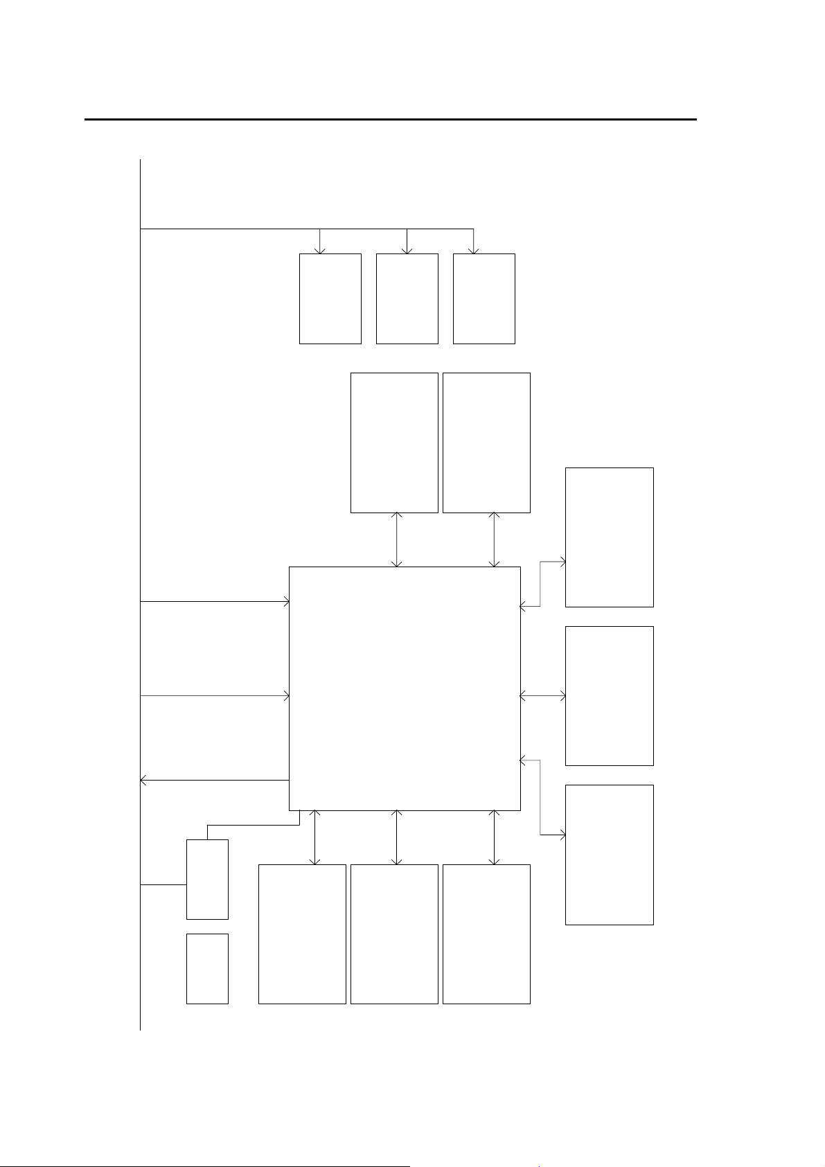
4-3. Function Block Diagram of GENLOCK Board
CN7
+3.3_SDI +3.3_SDI +3.3_SDI +3.3_SDI
+5V_PS +5V_PS +5V_PS +5V_PS
IIC_CLK,IIC_DATA,
PCB_ST
MH_SYNC-VA,MF_SYNC-VA,MV_SYNC-VA
CF_SYNC-VA,LVDS_RST-RA,FIFO_RST-A
FIFO_EN-A,NCS-A,SCLK-A,SDIN-A
DS1A_N:4bit
DS1A_P:4bit
DS0A_N:4bit
DS0A_P:4bit
IC11
LVCH16245
+3.3V +3.3V +3.3V +3.3V
CF_SYNC,LVDS_RST,
FIFO_EN-AB,NCS,
SCLK,SDIN
IC8
DS90CR217
+3.3V +3.3V
VO2-A:10bit
VO3-A:10bit
CN8
IIC_CLK,IIC_DATA,
PCB_ST
MH_SYNC-VA,MF_SYNC-VA,MV_SYNC-VA
CF_SYNC-VA,LVDS_RST-RA,FIFO_RST-A
FIFO_EN-A,NCS-A,SCLK-A,SDIN-A
IC12
LVCH16245
CF_SYNC,LVDS_RST,
FIFO_EN-AB,NCS,
SCLK,SDIN
IC10
DS90CR217
DS0B_N:4bit
DS1B_N:4bit
DS1B_P:4bit
VO2-B:10bit
VO3-B:10bit
DS0B_P:4bit
IC18
LVCH16245
CN9
IIC_CLK,IIC_DATA,
PCB_ST
MH_SYNC-VA,MF_SYNC-VA,MV_SYNC-VA
CF_SYNC-VA,LVDS_RST-RA,FIFO_RST-A
FIFO_EN-A,NCS-A,SCLK-A,SDIN-A
DS1C_N:4bit
DS1C_P:4bit
DS0C_N:4bit
DS0C_P:4bit
CF_SYNC,LVDS_RST,
FIFO_EN-AB,NCS,
SCLK,SDIN
IC15
DS90CR217
VO2-A:10bit
VO3-A:10bit
CN10
IIC_CLK,IIC_DATA,
MH_SYNC-VA,MF_SYNC-VA,MV_SYNC-VA
CF_SYNC-VA,LVDS_RST-RA,FIFO_RST-A
FIFO_EN-A,NCS-A,SCLK-A,SDIN-A
IC19
LVCH16245
CF_SYNC,LVDS_RST,
FIFO_EN-AB,NCS,
SCLK,SDIN
IC17
DS90CR217
+3.3V+3.3V
PCB_ST
DS1D_N:4bit
DS1D_P:4bit
DS0D_N:4bit
VO2-B:10bit
VO3-B:10bit
DS0D_P:4bit
IC7
+3.3V
CN1
To Mother Board
IC9
SCLK,SDIN
DS90CR217
+3.3V
VO0-B:10bit
VO1-B:10bit
IC34
IC31 HD64F7045
+3.3VD
+2.5VD
LVDS:162MHz
LVDS:162MHz
VOD-B_N:4bit
VOD-B_P:4bit
CN2
MH_SYNC,MF_SYNC,MV_SYNC
IC29
EP1K100FC
IC14
DS90CR217
+3.3V +3.3V
CN3
VO0-C:10bit
IC4
+3.3VD
+2.5VD
LVDS:162MHz
LVDS:162MHz
VOD-C_P:4bit
VOD-C_N:4bit
XC3S400
CF_SYNC,LVDS_RST,
FIFO_EN-AB,NCS,
SCLK,SDIN
IC16
DS90CR217
VO0-D:10bit
LVDS:162MHz
VOD-D_N:4bit
CN4
DS90CR217
VO0-A:10bit
VO1-A:10bit
CF_SYNC,LVDS_RST,
FIFO_EN-AB,NCS,
IC1
XC3S400
+3.3VD
+2.5VD
LVDS:162MHz
LVDS:162MHz
+5V_PS +5V_PS +5V_PS +5V_PS
VOD-A_P:4bit
VOD-A_N:4bit
ADM:32bit
LVDS:162MHz
VOD-D_P:4bit
+2.5VD
+3.3VD
+5V_PS
IC42
LP3965EMP
P1
AXH005AOX
+3.3_SDI
P3
AXH005AOX
19
Page 28
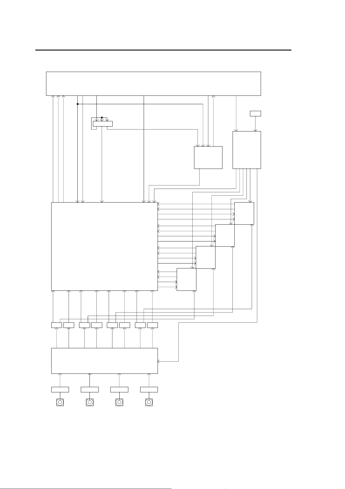
4-4. Function Block Diagram of BKDF-810 Board
CONNECTOR
( 8071 )
FPGA
[LVDS_CLK]
[LVDS_DATA]
( XC3S1500 )
CN8
IC102 = CLOCK BUFFER ( 74LVC245 )
[ADM_DATA]
[ADM_CTRL]
[LVDS_FRM]
IC11
FUNCTION
- VIDEO PROCESS ( BEFORE FRAME MEMORY )
> LUMINANCE GAIN
> CHROMINANCE GAIN
> LUMINANCE SETUP
> HUE CONTROL
> WHITE CLIP
> BLACK CLIP
> CHROMINANCE CLIP
[ADM_CLK]
IC22
[ADM_CLK2]
- LINE MEMORY ( USE MINIMUM DELAY MODE ONLY)
- FRAME SYNCHRONIZER CONTROLER
- VIDEO FREEZE CONTROLER( FRAME , ODD , EVEN )
- AUTO VIDEO FREEZE CONTROLER
- STILL STORE CONTROLER
[FVH]
[VSD-RCTRL]
[VSD-DATA]
[VD-WCTRL]
[VD-DATA3]
[VSC-RCTRL]
[VSC-DATA]
[VC-WCTRL]
[VC-DATA3]
[VSB-RCTRL]
[VSB-DATA]
[VB-WCTRL]
[VB-DATA3]
[VSA-RCTRL]
[VSA-DATA]
[VA-WCTRL]
[VA-DATA3]
IC27
FRAME
FIFO
MEMORY
[ADM_CLK2]
[ADM_CTRL]
IC14, 15, 101
[CONFIG]
IC29
[JTAG_OUT]
[JTAG_IN]
CONFIG ROM
FRAME
FIFO
MEMORY
IC28
FRAME
FIFO
[SYS_CLK]
[SYS_CLK2]
MEMORY
X2
[DBG_CLK]
IC16, 17, 18, 19, 20, 21
SYSTEM CLOCK DRIVERS
[SYS_CLK_D]
[SYS_CLK2]
[SYS_CLK2]
[SYS_CLK2]
[SYS_CLK2]
FRAME
FIFO
MEMORY
IC30
[VB-CLK2]
[VA-DATA2]
[VA-CLK2]
IC6
[VA-DATA]
IC23
[VB-CLK]
[VB-EQ]
IC2
SDI Input B
IC22
IC22, 23, 24, 25 = CLOCK BUFFER ( PI6CV304 )
IC6, 8, 9, 10 = DATA BUFFER ( 74LVCH16245 )
[VA-CLK]
SDI INDEPENDENT CLOCK
QUAD DESERIALIZER
( CYV15G0404RB )
[VA-EQ]
Equalizer
( GS9064 )
IC1
SDI Input A
SDI Input
[VB-DATA2]
IC8
[VB-DATA]
IC5
[VC-CLK2]
IC24
[VC-CLK]
[VC-DATA2]
[VC-DATA]
[VC-EQ]
IC3
SDI Input C
= field pulse + vertical pulse + horizontal pulse[FVH]
= 27MHz SYSTEM CLOCK[SYS_CLK]
= 27MHz CLOCK ( DEBUG CLOCK )[DBG_CLK]
[VD-CLK2]
= 27MHz DIFFERENTIAL SYSTEM CLOCK [ delayed 0.87 - 1.695ns ][SYS_CLK_D]
= 27MHz SYSTEM CLOCK [ delayed 2.335 - 4.91ns ][SYS_CLK2]
= CPU_CHIPSELECT & CPU_READY[ADM_CTRL]
= FPGA CONFIG DATA[CONFIG]
= 33MHz CPU_DATA_CLK
= 33MHz CPU_DATA_CLK [ delayed 16ns ]
[ADM_CLK2]
[ADM_CLK]
[ADM_DATA] = 33MHz CPU_DATA
= JTAG TDO FOR CPU WRITE CONFIG ROM
= JTAG TDI & TMS FOR CPU WRITE CONFIG ROM
[JTAG_OUT]
[JTAG_IN]
[VD-DATA2]
[VD-CLK2]
IC9
IC25
[VD-CLK]
IC10
[VD-DATA]
[VD-EQ]
IC4
SDI Input D
[VA-CLK2]
= 27MHz PIX_CLK
= 270MHz DIFFERENTIAL (Equalizer out)
[V*-EQ]
[V*-CLK]
"*" is video channel name [ A, B, C, D ]
[VB-CLK2]
= 4BIT FRAME MEMORY WRITE CONTROL DATA (synchronus PIX_CLK)[V*-WCTRL]
= 27MHz 10BIT DESCRAMBLE VIDEO DATA (synchronus PIX_CLK)
= BUFFERED 27MHz 10BIT SCRAMBLE VIDEO DATA (synchronus PIX_CLK)
[ delayed 1-4ns ]
= 27MHz BUFFERED PIX_CLK [ delayed 1-3ns ][V*-CLK2]
= 27MHz 10BIT SCRAMBLE VIDEO DATA (synchronus PIX_CLK)
[V*-DATA]
[V*-DATA3]
[V*-DATA2]
[VC-CLK2]
= 162MHz DDR 5 pair video data 162MHZ1 pair clock + 1 pair frame[LVDS_DATA]
= 4BIT FRAME MEMORY READ CONTROL DATA (synchronus SYS_CLK)[VS*-RCTRL]
= 162MHz 1 pair frame[LVDS_FRM]
= 162MHz 1 pair clock[LVDS_CLK]
[VS*-DATA] = 27MHz 10BIT DESCRAMBLE VIDEO DATA (synchronus SYS_CLK)
20
Page 29
4-5. Function Block Diagram of BKDF-811 Board
CN8
DSP_DATA:32bit
SYSYEM_CLK
5pair
LVDS,162MHz
FPGA
VCC0
VCCAUX,VCC0
VCCINT
+3.3V
+2.5V
+1.2V_core
VA_FM_RD:10bit
IC27
MS81V26000-12TB
+3.3V +3.3V
VA_FM_WD:10bit
S_CLK
CH1
VA_FM_CLK
IC11
XC3S1500-4FGG456C
VB_FM_RD:10bit
VB_FM_WD:10bit
S_CLK
CH2
VB_FM_CLK
SDA,SCLK
IC28
MS81V26000-12TB
I2C BUS
DV_1:10bit
SDA,SCLK
+1.8V
+3.3V
ADV7189
DECORDER1
DV_2:10it
SDA,SCLK
+1.8V
+3.3V
ADV7189
DECORDER2
+1.8VA
+1.8VD
+2.5V+3.3VA
+5.0VA
Input Amp Filter
+5V
Input Amp Filter
-5V
+5V
Input Amp Filter
-5V
+5V
Input Amp Filter
-5V
+5V
-5V
+3.3VD
+1.2VCORE
-5.0VA
+5.2V
21
Page 30
4-6. Function Block Diagram of BKDF-840 Board
+5V
To Main Card
DC/DC P4
BSV-H
+5V to +1.5V
DC/DC P2
AXH005AOX
+5V to +2.5V
I/O POWER
(XILINX LVDS &
Configuration)
DC/DC P5
BSV-H
+5V to +3.3V
I/O & SRAM POWER
CORE POWER
*Write Only*
Transaction BUS
32bits 2.5V LVCMOS
VIDEO IN 17ch
LVDS 162MHz DDR
VIDEO OUT 4ch
LVDS 162MHz DDR
IC5 & IC7
Synchronous SRAM
Synchronous SRAM
CY7C1372D
Input DVE 16ch & Pre-Combiner
XC2VP30-5FF1152
IC1
CY7C1372D
IC6 & IC8
Synchronous SRAM
CY7C1372D
Synchronous SRAM
CY7C1372D
IC9 & IC11IC10 & IC12
JTAG CHAIN
for update FGPA data
REG IC21
Cofiguration ROM
XCF16VOG48
IC4
3.3V to 1.8V
to XCF16( IC4 )
CY7C1372D
IC18 & IC20
Synchronous SRAM
Synchronous SRAM
CY7C1372D
22
IC17 & IC19
Synchronous SRAM
CY7C1372D
IC14 & IC16
Synchronous SRAM
CY7C1372D
IC13 & IC15
Page 31

4-7. Function Block Diagram of BKDF-860 Board
IC14
GS9068
SDD_N
SDI_OUT4
+1.8VD_C
SDD_P
+3.3VD
IC12
GS9068
SDC_N
SDI_OUT3
SDC_P
NRST_AB,NCS_AB,SCLK_AB,SDIN_AB,
H-SYNC_AB,V-SYNC_AB,F-SYNC_AB,
FIFO-EN_AB
IC11
GS9092
IC10
GS9068
SDI_OUT2
+3.3VD
+1.8VD_A
IC8
GS9068
SDI_OUT1
SDA_P
SDA_N
IC7
GS9092
NRST_CD,NCS_CD,SCLK_CD,SDIN_CD,
H-SYNC_CD,V-SYNC_CD,F-SYNC_CD,
FIFO-EN_CD
+3.3VD
+3.3V_LVDS
+3.3VD
+1.8VD_D
IC3
DS90CR21BAMTD
VDD_:10bit
VDC_:10bit
DS1_N:4bit
DS1_P:4bit
IC13
GS9092
NRST_AB,NCS_AB,SCLK_AB,SDIN_AB,
H-SYNC_AB,V-SYNC_AB,F-SYNC_AB,
FIFO-EN_AB
IC1
DS90CR21BAMTD
+3.3V_LVDS
CN1
To Genlock Card
VDB_:10bit
VDA_:10bit
DS0_N:4bit
DS0_P:4bit
+5V
+3.3VD
+1.8VD_B
SDB_N
SDB_P
IC9
GS9092
NRST_CD,NCS_CD,SCLK_CD,SDIN_CD,
H-SYNC_CD,V-SYNC_CD,F-SYNC_CD,
FIFO-EN_CD
NRST_AB,NCS_AB,SCLK_AB,SDIN_AB,
H-SYNC_AB,V-SYNC_AB,F-SYNC_AB,
FIFO-EN_AB
IC2
LVCH16245
+3.3VD+3.3VD
ANRESET,ANCS,ASCLK,ASDIN,AMH-SYNC,
AMV-SYNC,AMF-SYNC,AFIFO-EN
+1.8V_C
+1.8VD +1.8VD
NRST_CD,NCS_CD,SCLK_CD,SDIN_CD,
H-SYNC_CD,V-SYNC_CD,F-SYNC_CD,
FIFO-EN_CD
+1.8VD
IC4
+3.3VD
L11
+1.8V_B
+1.8VD
+1.8V_A
+1.8VD
LP3965EMP
+3.3_LVDS
+3.3VD
+1.8V_D
SAGND_C
L12
L7
L3
L1
L8
L4
L2
L15
SAGND_B
SAGND_ALVDS_GND
SAGND_D
L16
23
Page 32

4-8. Function Block Diagram of BKDF-861 Board
Pb / G
Composite1 / Y / R
Pr / B
Composite2
AD8180
low pass filter
Video Encorder
CH1
Analog Devices
ADV7321
offset voltage
pedestal fix & low pass filter
cntroll signal (for video encorder & AD8180)
pedestal fix & low pass filter
10bits 27MHz
low pass filter
Video Encorder
CH1
Analog Devices
ADV7321
10bits 27MHz
I2C BUS
IC2
DS90CR218
LVDS 162MHz 4 paires 10 controll signals multiplexed
LVDS 162MHz 4paires 2 video channnel multiplexed
24
IC3
DS90CR218
+5.2V
+3.3V
+2.5V
LP3965EMP
LT1175
-6.0V
Page 33

5. Adjustment Procedure of Each Board
5-1. Adjustment of CPU Board
Default Setting of DIP switches and Jumpers on the BKDF-810 Board
SW1 ( Zone on board: J4 )
Setting at ex-factory
Depending on the option configuration, the setting differs.
In case of standard configuration ( without option ), all of bits are set to OFF.
Content of Setting
Referring to the table below, set to meet the option installation.
For location of each slot, refer to the figure on the next page.
SW No Content of Setting
1
2
3
4
5
6
7
8 OFF: Install nothing in the slot DS1.
ON: Install the BKDF-810 or BKDF-811 in the slot A.
OFF: Install nothing in the slot A.
ON: Install the BKDF-810 or BKDF-811 in the slot B.
OFF: Install nothing in the slot B.
ON: Install the BKDF-811 in the slot C.
OFF: Install nothing in the slot C.
ON: Install the BKDF-811 in the slot D.
OFF: Install nothing in the slot D.
ON: Install the BKDF-811 in the slot A.
OFF: Install the BKDF-810 or nothing in the slot A.
ON: Install the BKDF-811 in the slot B.
OFF: Install the BKDF-810 or nothing in the slot B.
ON: Install the BKDF-840 in the slot DS2.
OFF: Install nothing in the slot DS2.
SW1JP3 JP4 SW2
25
Page 34

DS1
Slot C
Slot A
Slot D
DS2
Slot B
SW2 ( Zone on board: N1 )
Setting at ex-factory
All of bits: OFF
Content of Setting
No need to change the setting. Use the factory setting as is.
JP3 ( Zone on board:E3 )
Setting at ex-factory
MAIN Board
Slot DS2
BKDF-840
1 2 3 4 5 6 7 8
Short-circuit pins 1 and 2 with jumper plug.
Content of Setting
No need to change the setting. Use the factory setting as is.
JP4 (Zone on board:L1)
Setting at ex-factory
Short-circuit pins 1 and 2 with jumper plug.
Content of Setting
No need to change the setting. Use the factory setting as is.
26
Page 35

5-2. Adjustment of MAIN Board
Default Setting of DIP switches on the MAIN Board
SW2 SW1
SW1 ( Zone on board:K1 )
Setting at ex-factory
ON: 1,2,3,8, OFF: 4,5,6,7
Content of Setting
No need to change the setting. Use the factory setting as is.
SW2 ( Zone on board:J1 )
Setting at ex-factory
ON: 1,2,3,8, OFF: 4,5,6,7
Content of Setting
No need to change the setting. Use the factory setting as is.
1 2 3 4 5 6 7 8
1 2 3 4 5 6 7 8
27
Page 36

5-3. Adjustment of GENLOCK Board
Default Setting of DIP switches on the GENLOCK Board ( E03012-1 and later )
S1 ( Zone on board: K2 )
Setting at ex-factory
ON: 3,4,5,6,7,8, OFF: 1,2
Content of Setting
No need to change the setting. Use the factory setting as is.
S2 ( Zone on board: N6 )
Setting at ex-factory
All of bits: OFF
Content of Setting
No need to change the setting. Use the factory setting as is.
S1 S2 S3
1 2 3 4 5 6 7 8
1 2 3 4 5 6 7 8
S3 ( Zone on board: W3 )
Setting at ex-factory
ON: 1,2,6,7, OFF: 3,4,5,8
Content of Setting
No need to change the setting. Use the factory setting as is.
28
1 2 3 4 5 6 7 8
Page 37

5-4. Adjustment of BKDF-810 Board
Default Setting of DIP switches on the BKDF-810 Board
S1 ( Zone on board: Q2 )
Setting at ex-factory
ON: 1,2,3,4, OFF: 5,6,7,8
Content of Setting
No need to change the setting. Use the factory setting as is.
S2 ( Zone on board: D1 )
Setting at ex-factory
ON: 2,3,4, OFF: 1,5,6,7,8
Content of Setting
No need to change the setting. Use the factory setting as is.
S1 S2
1 2 3 4 5 6 7 8
1 2 3 4 5 6 7 8
29
Page 38

5-5. Adjustment of BKDF-811 Board
Default Setting of DIP switch on the BKDF-811 Board
S1 ( Zone on board:P5 )
Setting at ex-factory
ON: 4, OFF: 1,2,3,5,6,7,8
Content of Setting
No need to change the setting. Use the factory setting as is.
S1
1 2 3
4 5 6
7
8
ON
30
Page 39

5-6. Adjustment of BKDF-840 Board
Default Setting of DIP switch on the BKDF-840 Board
SW1
SW1 ( Zone on board: B7 )
Setting at ex-factory
ON: 1,2,3,8, OFF: 4,5,6,7
Content of Setting
No need to change the setting. Use the factory setting as is.
1 2 3 4 5 6 7 8
31
Page 40

5-7. Adjustment of BKDF-860 Board
No setting item
5-8. Adjustment of BKDF-861 Board
No setting item
32
Page 41

w
6. Method of Board Replacement/Addition
6-1. Removal/Installation of Shield Plate
In this section, the method of removal and installation of shield plate required when replacing/adding
each board is explained.
6-1-1. Removal of Shield Plate
1) Referring to the figure below, unscrew four screws ( 3×6mm ) and remove the retainer fixing
the board in the slot.
DFS-800 Rear Panel
1
2
3
4
2) Remove the shield plate from the slot where the target board is installed.
From top to bottom, slots are named 1 to 4. For board in each slot, refer to the table below.
When removing the shield plate, widen the black handles and draw the shield plate toward you.
Screw Scre
G
P
M
P
2
1
M
G
P
E
R
V
L
C
A
N
V
I
D
E
O
O
U
T
1
V
I
D
E
O
I
N
E
3
4
2
2
A
X
U
A
1
5
A
U
X
U
A
3
X
U
4
X
8
6
7
1
N
O
K
C
N
B
E
O
B
G
I
L
1
2
3
2
4
T
U
U
O
T
O
Retainer Retainer
Slot Board
Slot 1 GENLOCK, BKDF-860, BKDF-861
Slot 2 MAIN, BKDF-840
Slot 3 BKDF-810, BKDF-811
Slot 4 CPU, BKDF-811
1
E
R
O
M
T
S
E
R
4
2
2
-
1
T
2
E
R
O
I
D
2
3
4
0
H
/
6
I
z
0
N
5
V
0
0
-
C
1
2
4
0
A
33
Page 42

r
r
6-1-2. Installation of Shield Plate
1) Return the shield plate to the original slot. When returning the shield plate, hook the claws of
black handles to the unit and turn the handles inwards.
2) Install the retainers removed in [ 6-1-1. Removal of Shield Plate ] and tighten them with screws.
Screw Screw
E
R
E
X
M
G
P
V
I
D
E
O
O
U
T
1
V
I
D
E
O
I
N
Retaine
P
V
2
1
M
G
P
3
2
U
A
X
U
L
C
4
A
A
N
1
5
4
X
2
A
A
U
3
X
U
7
8
6
1
N
T
K
C
N
B
E
O
B
G
I
O
L
U
2
1
2
3
4
U
O
T
O
Retaine
1
R
2
3
4
S
E
R
O
4
M
E
2
2
-
T
R
O
I
D
T
2
E
1
0
H
V
/
6
I
z
0
0
-
N
5
2
4
0
0
C
1
A
Caution
When installing the shield plates of slot 1 and slot 2, they may not be installed.
In this case, refer to [ 6-1-3. Caution on Insertion of Shield Plate ] and install them
34
Page 43

6-1-3. Caution on Insertion of Shield Plate
Shield Plate of Slot1
When removing the shield plate of slot 1 alone and returning it in the original slot, the shield plate
may not be inserted.
In this case, insert it in the following procedure.
1) Remove the shield plate of slot 2.
With this, the pressure to the shield plate of slot 1 from the bottom is released.
2) Loosen the screw fixing the top cover.
With this, the top cover can be lifted upward.
3) While holding down the shield plate of slot 1 from the top, insert it.
4) Tighten the screw fixing the top cover.
Screw
Shield Plate of Slot 2
When the BKDF-840 board is already installed, if the shield plate of slot 2 is inserted, the heat sink
on the BKDF-840 board may touch the shield plate of slot 1.
In this case, lift the shield plate of slot 1 and insert the shield plate of slot 2.
Lift up the slot 1.
Slot 1
Slot 2
Insert the shield plate.
35
Page 44

6-2. Replacement of CPU Board
Install the CPU board in the 4th slot of DFS-800 from the top. To install the CPU board, remove the
shield plate of slot 4 from the rear of DFS-800 and insert the CPU board in the slot.
For removal and installation of shield plate, refer to [ 6-1. Removal/Installation of Shield Plate ].
6-2-1. Removal of CPU Board
1) Referring to the figure below, unscrew 4 screws fixing the CPU board to the shield palte.
( W SEMS screw 3×6mm 4 locations )
2) Unscrew one screw fixing the shield plate and BNC connector.
( Binding screw 2.6×6mm 1 location )
3) While sliding the CPU board, remove the CPU board from the shield plate
36
Page 45

6-2-2. Installation of CPU Board
1) Install the CPU board, aligning the BNC connector of CPU board with the hole on the shield
plate.
2) Fix the shield plate and BNC connector with the binding screw ( 2.6×6mm ).
3) Fix the CPU board to the shield plate with four W SEMS screws ( 3×6mm ).
6-2-3. Setting
Referring to [ 5-1. Adjustment of CPU board ], set the DIP switch to meet the option configuration.
37
Page 46

6-3. Replacement of MAIN Board
Install the MAIN board in the 2nd slot of DFS-800 from the top. To install the MAIN board, remove
the shield plate of slot 2 from the rear of DFS-800 and insert the MAIN board in the slot.
For removal and installation of shield plate, refer to [ 6-1. Removal/Installation of Shield Plate ].
6-3-1. Removal of MAIN Board
1) Referring to the figure below, unscrew 6 screws fixing the Main board to the shield palte.
( W SEMS screw 3×6mm 6 locations )
2) If the BKDF-840 is installed, remove the MAIN board from the shield plate, sliding the MAIN
board.
MAIN CARD
Slot 2
BKDF-840
38
Page 47

6-3-2. Installation of MAIN Board
1) Before installing the board, check the DIP switch setting. Referring to [ 5-2. Adjustment of
MAIN Board ], set the DIP switch.
2) Aligning the screw holes with the screw holes on the shield plate, install the MAIN board.
If the BKDF-840 board is installed, slide the MAIN board and connect the connector.
3) Fix the MAIN board to the shield plate with six W SEMS screws ( 3×6mm ).
MAIN CARD
Slot 2
BKDF-840
39
Page 48

6-4. Replacement of GENLOCK Board
Install the GENLOCK board in the 1st slot of DFS-800 from the top. To install the GENLOCK board,
remove the shield plate of slot 1 from the rear of DFS-800 and insert the GENLOCK board in the
slot.
For removal and installation of shield plate, refer to [ 6-1. Removal/Installation of Shield Plate ].
6-4-1. Removal of GENLOCK Board
1) Referring to the figure below, unscrew six screws fixing the GENLOCK board to
the shield plate. ( 3×6mm W SEMS screw 6 locations )
2) Referring to the figure below, remove the GENLOCK board from the shield plate while
sliding slowly the GENLOCK board. Finally remove the he GENLOCK board completely.
Do not remove the GENLOCK board and option board together. When removing, the
Caution
Protrusion
strong force is required and the GENLOCK board is suddenly removed. At this
moment, The components mounted on the back side of board may hit the
protorusions, resulting in damage.
GENLOCK Board
Protrusion
Shied plate
40
Page 49

6-4-2. Installation of GENLOCK Board
1) Before installing the board, check the DIP switch setting. Referring to [ 5-3. Adjustment of
GENLOCK Board ], set the DIP switch.
2) Sliding the GENLOCK board with caution, install the GENLOCK board to the shield plate.
Engage the GENLOCK board firmly.
3) Fix the GENLOCK board to the shield plate with 6 screws ( 3×6mm W SEMS ) removed in
[ 6-4-1. Removal of GENLOCK Board ].
GENLOCK CD
Shield Plate
41
Page 50

6-5. Replacement/Addition of BKDF-810 Board
Install the BKDF-810 board in the 3rd slot of DFS-800 from the top. To install the GENLOCK board,
remove the shield plate of slot 3 from the rear of DFS-800 and insert the BKDF-810 board in the
slot.
For removal and installation of shield plate, refer to [ 6-1. Removal/Installation of Shield Plate ].
6-5-1. To Begin with
For input board of DFS-800, the BKDF-810 and BKDF-811 can be used. Refer to the
combination list of input board and installation slocation below and install the board in the
appropriate slot. After changing the configuration, be sure to set the DIP switch.
Combination List of Input Board and Installation Location
BKDF-810
BKDF-810
BKDF-810
BKDF-810
BKDF-810
BKDF-810
BKDF-810
BKDF-810
BKDF-810
Slot S
Slot C
Slot S'
Slot D
Slot A Slot B
DFS-800 Rear Location of Slot
Slot
Standard Option
S S' A B C D Digital Analog To tal
( 1-4 )
( 1-4 )
( 1-4 )
( 1-4 )
( 1-4 )
( 1-4 )
( 1-4 )
( 1-4 )
( 1-4 )
BKDF-810
( 5-8 )
BKDF-810
( 5-8 )
BKDF-810
( 5-8 )
BKDF-810
( 5-8 )
BKDF-810
( 5-8 )
BKDF-810
( 5-8 )
BKDF-810
( 5-8 )
BKDF-810
( 5-8 )
BKDF-810
( 5-8 )
- - - - SDI x 8 AI x 0 8
BKDF-811
( 9,10 )
BKDF-811
( 9,10 )
BKDF-811
( 9,10 )
BKDF-811
( 9,10 )
BKDF-810
( 9-12 )
BKDF-810
( 9-12 )
BKDF-810
( 9-12 )
BKDF-810
( 9-12 )
- - - SDI x 8 AI x 2 10
BKDF-811
( 11,12 )
BKDF-811
( 11,12 )
BKDF-811
( 11,12 )
- - - SDI x 12 AI x 0 12
-
-
BKDF-810
( 13-16 )
- - SDI x 8 AI x 4 12
BKDF-811
( 13,14 )
BKDF-811
( 13,14 )
BKDF-811
( 13,14 )
BKDF-811
( 13,14 )
- - SDI x 16 AI x 0 16
- SDI x 8 AI x 6 14
BKDF-811
( 15,16 )
- SDI x 12 AI x 2 14
BKDF-811
( 15,16 )
Number of input
SDI x 8 AI x 8 16
SDI x 12 AI x 4 16
42
Page 51

6-5-2. Removal of BKDF-810 Board
1) Referring to the figure below, unscrew 4 screws fixing the BKDF-810 board to the shield plate.
( W SEMS screw 3×6mm 4 locations )
2) Unscrew 4 screws fixing the shield plate and BNC connector.
( Binding screw 2.6×6mm 4 locations )
3) Sliding the BKDF-810 board, remove the BKDF-810 board from the shield plate.
43
Page 52

6-5-3. Installation of BKDF-810 Board
1) Before installing the board, check the DIP switch setting. Referring to [ 5-4. Adjustment of
BKDF-810 Board ], set the DIP switch.
2) Referring to the combination list on page 42, confirm the slot to be installed.
3) When installing newly the BKDF-810 board, unscrew 2 screws (3x6mm ) at both sides of blank
panel on the rear panel of shield plate and remove the blank panel.
4) Aligning the holes on the shield plate with BNC connectors on the BKDF-810 board, install the
BKDF-810 board. First, fix the shield plate and BNC connectors with 4 binding screws
(2.6×6mm). At this moment, be careful not to dislocate the screw holes.
5) Fix the BKDF-810 board to the shield plate with 4 W SEMS screws ( 3×6mm ).
44
Page 53

6-5-4. Setting and Confirmation of Operation
Referring to [ 5-1. Adjustment of CPU Board ], set SW1 to meet the input board configuration.
Turn on the power and display [ STATUS ]. Then, confirm that the BKDF-810 board is recognized.
And confirm that the input extended can be selected.
45
Page 54

6-6. Replacement/Addition of BKDF-811
Install the BKDF-811 board in the 3rd slot or 4th slot of DFS-800 from the top. To install the
BKDF-811 board, remove the shield plate of slot 3 or slot 4 from the rear of DFS-800 and insert the
BKDF-811 board in the slot.
For removal and installation of shield plate, refer to [ 6-1. Removal/Installation of Shield Plate ].
6-6-1. To Begin with
For input board of DFS-800, the BKDF-810 and BKDF-811 can be used. Refer to the
combination list of input board and installation slot on page 42, and install the board in the
appropriate slot. After changing the configuration, be sure to set the setting of DIP switch on the
CPU board.
When using two composite inputs of the analog input board, use two connectors at both ends.
When using Y, B-Y, R-Y, use three connectors from the left side. The type of signal is displayed
on the ornamental panel.
46
Page 55

Y
6-6-2. Removal of BKDF-811 Board
1) Referring to the figure below, unscrew four screws fixing the BKDF-811 board to the shield
plate. ( W SEMS screw 3×6mm 4 locations )
2) Unscrew four screws fixing the shield plte and BNC connector.
( Binding screw 2.6×6mm 4 locations )
3) Sliding the BKDF-811 board, remove the BKDF-811 board from the shield plate.
Ornamental Panel
COMP/Y B-
R-Y COMP
47
Page 56

6-6-3. Installation of BKDF-811 Board
1) Before installing the BKDF-811 board, check the DIP switch setting.
Referring to [ 5-5. Adjustment of BKDF-811 Board ], set the DIP switch.
2) Referring to the combination list on page 42, confirm the slot to be installed.
3) Affix the input number seal to the ornamental panel to identify the input number to be extended.
Example: In case of installing the analog input board to In09 and In10
COMP/Y B-Y R-Y COMP
9 10
4) When adding newly the BKDF-811 board, unscrew two screw ( 3 x 6mm ) at both side of blank
panel on the rear of shield panel and remove the blank panel.
48
Page 57

5) Aligning the holes on the shield plate with the BNC connectors on the analog input board,
install the BKDF-811 board. First, fix the shield plate and BNC connectors with four binding
screws ( 2.6×6mm ). At this moment, be careful not to dislocate the screw holes on the board.
Ornamental panel
6) Fix the board to the shield plate with four W SEMS screws ( 3×6mm ).
Installation in slot 3
COMP/Y B-Y R-Y COMP
COMP/Y B-Y R-Y COMP
Installation in slot 4
6-6-4. Setting and Confirmation of Operation
Referring to [ 5-1.Adjustment of CPU Board ], set the DIP switch SW1 to meet the
configuration of input board.
Turn on the power and disply [ STATUS ]. Then, confirm that the BKDF-811 board is
recognized. And confirm that the input extended can be selected.
49
Page 58

r
r
6-7. Replacement/Addition of BKDF-840
Install the BKDF-840 board in the 2nd slot ( slot 2 ) of DFS-800 from the top. To install the
BKDF-840 board, remove the shield plate of slot 2 from the rear of DFS-800 and install the
BKDF-840 board in the slot.
For removal/installation of shield plate, refer to [ 6-1. Removal/Installation of Shield Plate ].
6-7-1. Removal of BKDF-840 Board
1) Referring to the procedure and figure below, remove the BKDF-840 board.
1. Move the board in the arrow direction ① and disconnect the connectors from the Main
board.
2. Lift up the connector side of board and pull out the board.
①
②
connecto
rubber
Install Procedure
connecto
50
Page 59

6-7-2. Installation of BKDF-840 Board
1) Before installing the BKDF-840 board, check the DIP switch setting.
Referring to [ 5-6. Adjustment of BKDF-840 Board ], set the DIP switch.
2) Confirm the location to be installed. Install the BKDF-840 board in the slot 2.( See the figure
below. )
3) If the heat radiation rubber is not installed, install the heat radiation rubber. To place the heat
radiation rubber correctly, draw the positioning drawing and then place the rubber.
According to the procedure below, install the heat radiation rubber in between the board ( back
side of IC1 ) and shield plate.
1. Copy [Positioning Drawing] on page 51 and cut off the outer frame and broken lines.
2. Cut four corners along the broken line. This sheet can be placed on the shield plate.
3. Peel the films off both sides of heat radiation rubber.
4. Place the positioning drawing on the shield plate and the then the heat radiation rubber at the
end of positioning drawing so that the position of holes is matched.
5. Remove the positioning drawing.
4) Referring to the procedure and figure below, install the board.
1. Insert the rear side ( opposite to the connector ) of board under the folded portion of shield
plate.
2. Move the board forward and connect the connectors.
Figure of board implementation procedure
②
①
MAIN CARD
Heat radiation rubber
Slot 2
BKDF-840
Connector
Connector
51
Page 60

6-7-3. Setting and Confirmation of Operation
Referring to [5-1. Adjustment of CPU Board], set the DIP switch SW1 to meet the configuration of
BKDF-840 board.
Turn on the power and display [STATUS] menu. Then, confirm that the BKDF-840 board is
recognized.
6-7-4. Positioning Drawing for affixing the rubber
MAIN CARD
ラバー貼り付け場所
Location of Rubber Affix
Positioning Drawing
位置だし図
52
Page 61

6-8. Replacement/Addition of BKDF-860 Board
Install the BKDF-860 board in the 1st slot ( slot 1 ) of DFS-800 from the top. To install the
BKDF-860 board, remove the shield plate of slot 1 from the rear of DFS-800 and install the
BKDF-860 board in the slot 1.
To install the BKDF-860 board, the GENLOCK board needs to be removed from the
shield plate. Before starting the work of replacement/addition of BKDF-860 board,
Caution
6-8-1. To Begin with
For output board of DFS-800, the BKDF-860 and BKDF-861 can be used.
Refer to the combination list of output board installation location below and install the board in
the appropriate location.
Combination List of Output Board Installation Location
refer to [6-4-1. Removal of GENLOCK Board ] and remove the GENLOCK board.
After finishing the work, refer to [6-4-2. Installation of GENLOCK Board ] and
install the GENLOCK board.
Location of slot on the rear of DFS-800
Slot S
Slot S'
Slot
Standard Option
S S' A B Digital Analog Total
BKDF-860
( 1-4 )
BKDF-860
( 1-4 )
BKDF-860
( 1-4 )
BKDF-860
( 1-4 )
BKDF-860
( 1-4 )
BKDF-860
( 1-4 )
BKDF-860
( 5-8 )
BKDF-860
( 5-8 )
BKDF-860
( 5-8 )
BKDF-860
( 5-8 )
BKDF-860
( 5-8 )
BKDF-860
( 5-8 )
- - SDO x 8 AO x 0 8
BKDF-861
( 9,10 )
BKDF-861
( 9,10 )
BKDF-860
( 9-12 )
BKDF-860
( 9-12 )
BKDF-860
( 9-12 )
Slot A Slot B
Number of output
- SDO x 8 AO x 2 10
BKDF-861
( 11,12 )
- SDO x 12 AO x 0 12
BKDF-861
( 13,14 )
BKDF-860
( 13-16 )
SDO x 8 AO x 4 12
SDO x 12 AO x 2 14
SDO x 16 AO x 0 16
53
Page 62

6-8-2. Removal of BKDF-860 Board
1) Referring to the figure below, unscrew two screws fixing the BKDF-860 board to the shield
plate.
( W SEMS screw 3×6mm 2 locations )
2) Referring to the figure below, unscrew two screws fixing the shield plate and BNC connector.
( Binding screw 2.6×6mm 2 locations )
3) Lifting up the BKDF-860 board a little, remove the BKDF-860 board in the arrow direction..
Caution
<- DFS-800 Rear Side
3)
If the BKDF-860 board is removed horizontally, the components mounted on the back
side of board may hit the protorusions, resulting in damage.
1)
BKDF-860 Board
2)
<- DFS-800 Rear Side
Shield Plate
protrus
54
Page 63

6-8-3. Installation of BKDF-860 Board
1) Referring to the combination list on page 53, confirm the location to be installed.
2) When adding newly the BKDF-860 board, unscrew two binding screws ( 3 x 6 mm ) at the both
sides of blank panel on the rear panel of shield plate and remove the blank panel.
3) Aligning the holes on the shield plate with the BNC connectors on BKDF-860 board, install the
BKDF-860 board. First, fix the shield plate and BNC connectors with two binding screws ( 2.6
x 6 mm ).At this moment, be careful not to dislocate the screw holes on the board.
4) Fix the BKDF-860 board to the shield plate with two W SEMS screws ( 3×6mm ).
3)
<- DFS-800 Rear Side
Shield Plate
4)
<- DFS-800 Rear Side
BKDF-860 Board
6-8-4. Confirmation of Operation
Turn on the power and display [ STATUS ] menu. Then, confirm that the BKDF-860 board is
recognized. And set the output setting of AUX output added and confirm that the video is correctly
outputted.
55
Page 64

6-9. Replacement/Addition of BKDF-861 Board
Install the BKDF-861 board in the 1st slot ( slot 1 ) of DFS-800 from the top. To install the
BKDF-861 board, remove the shield plate of slot 1 from the rear of DFS-800 and install the
BKDF-861 board in the slot 1.
For removal and installation of the shield plate, refer to [ 6-1. Removal/Installation of Shield Plate ].
To install the BKDF-861 board, the GENLOCK board needs to be removed from the
shield plate. Before starting the work of replacement/addition of BKDF-861 board,
Caution
6-9-1. To Begin with
For output board of DFS-800, the BKDF-860 and BKDF-861 can be used. Refer to the
combination list of output board installation location on page 53 and install the board in the
appropriate location.
When two composite outputs on the analog output board are used, use two connectors at both
sides. When using Y, B-Y, R-Y, use three connectors from the left side. The type of signal is
displayed on the ornamental panel.
refer to [6-4-1. Removal of GENLOCK Board ] and remove the GENLOCK board.
After finishing thework, refer to [6-4-2. Installation of GENLOCK Board ] and install
the GENLOCK board.
56
Page 65

6-9-2. Removal of BKDF-861 Board
1) Referring to the figure below, unscrew two screws fixing the BKDF-861 board to the shield
plate. ( W SEMS screw 3×6mm 2 locations )
2) Unscrew two screws fixing the shield plate and BNC connectors.
( Binding screw 2.6×6mm 2 locations )
3) Lifting up the BKDF-861 board a little, remove the BKDF-861in the arrow direction.
Caution
If the BKDF-861 board is removed horizontally, the components mounted on the back
side of board may hit the protorusions, resulting in damage.
1)
2)
<- DFS-800 Rear Side
Ornamental
<- DFS-800 Rear Side
COMP/Y/G B-Y/B R-Y/R COMP
BKDF-861 Board
Shield Plate
3)
protru
57
Page 66

6-9-3. Installation of BKDF-861 Board
1) Referring to the combination list on page 53, confirm the location to be installed.
2) Affix the output number seal to the ornamental panel to identify the location to be installed.
Slot A
Slot B
Select either one.
3) When adding newly the board, unscrew two screws ( 3 x 6 mm ) at both sides of blank panel on
the back side of shield plate and remove the blank panel.
COMP/Y/G B-Y/B R-Y/R COMP
AUX5 AUX 6
AUX7 AUX 8
AUX9 AUX 10
58
Page 67

4) Aligning the holes on the shield plate with the BNC connectors on analog output board, install
lthe board. First, fix the shield plate and BNC connectors with two binding screws ( 2.6 x 6
mm ). Before fixing, be careful not to dislocate the screw holes on the board.
5) Fix the board to the shield case with two W SEMS screws ( 3×6mm ).
<- DFS-800 Rear Side
Onaramental
4)
COMP/Y/G B-Y/B R-Y/R COMP
Shield Plate
5)
<- DFS-800 Rear Side
BKDF-861 Board
6-9-4. Confirmation of Operation
Turn on the power and display [ STATUS ] menu. Then, confirm that the BKDF-861 board is
recognized. And set the output setting for AUX output added and confirm that output video is
correctly outputted.
59
Page 68

7. Update of Firmware/Software
7-1. Procedure of Version Confirmation
7-1-1. Confirmation of GUI Version
1) After selecting [ system ] or [ status ] on Delegate row ( on the PGM row ), keep pressing the
right [ > ] button as far as it goes to display the Update menu.
2) Confirm the version that follows after “CP=”.
Update
CP=x.xx DPU Cal. TG:XXX
7-1-2. Confirmation of CPU1 Version
1) After selecting [system] or [status] on Delegate row ( on the PGM row ), press the left and right
[ < ] [ > ] butons to display the Version menu.
2) Confirm the version that follows after “CPU1=”.
Version
CPU1=xxxx
60
Page 69

7-2. Update Procedure
1) Prepare the USB memory ( 128MB and more ) containing the update data.
2) At this moment, name the data file the designated name and place it at the root of USB memory.
For location to be updated and filename, see the table below.
Location to be
updated
GUI OuPanel.exe, update.txt,
dme_pat.bmp, wip_pat.bmp, msk_pat.bmp
* In future, files other than above will be added. Therefore, prepare
the USB memory so that the version upgrade data provided by
FOR. A can be saved.
CPU cpu.out ( CPU_1 )
cpu.xsvf ( CPU_2 )
MAIN main1.xsvf ( MAIN_1 )
main2.xsvf ( MAIN_2 )
GENLOCK output.xsvf ( OUTPUT_1, 2 )
BKDF-810 ( SDI ) input.xsvf ( SDI_1, 2, 3, 4 )
BKDF-811 ( AI ) ai.xsvf ( AI_3_1, 2, AI_4_1, 2 )
BKDF-840 ( DS ) ds.xsvf ( InDME_2 )
3) Connect the DFS-800 Control Panel / Processor and start up them.
Filename
Caution
4) Confirm that the units start up normally. To confirm that the Control Panel communicates with the
Processor, check that the LED of RJ-45 connector of either Control Panel or Processor blinks. If
the LED does not blink, turn off and on the power of Processor.
5) Connect the prepared USB memory to the USB connector on the top of Control Panel. Do not
connect anything to the USB connector on the back of Control Panel.
6) After this, go to step [ 7-3 ] when updating the GUI or go to step [ 7-4 ] when updating other than
GUI.
If the power failure occurs during update or the communication is disrupted, the
DFS-800 may not start up. Be careful for the power cord or LAN cable not to be
disconnected during update. If the claw of LAN cable is broken, replace it with a new
cross cable.
61
Page 70

7-3. Update of GUI Software
1) After selecting [system] or [status] on Delegate row ( on the PGM row ), keep pressing the right
[ > ] button as far as it goes to display the Update menu.
2) Press F1 straigthtly for about 1 second, and then the access to the USB memory starts, beeping
faintly. ( The LED of USB memory blinks when accessed. ) After finishing the update of GUI
program, the Control Panel starts automatically rebooting, displaying the reboot message. At this
moment, plug out the USB memory once. The unit re-starts up in about 120 seconds.
3) To display the update menu again, operate the same manner as done in step 1 ).
If the GUI version that follows after ”CP=” is the new one, the update is normaly finished.
If the version before the update is displayed, try to update the GUI.
7-4. Update of Board Firmware
1) After selecting [system] or [status] on Delegate row (on the PGM row), keep pressing the right [ > ]
button as far as it goes to display the Update menu.
2) Select the target with F3 and press F3 straigthtly for about 1 second
3) The USB memory is accessed ( The LED of USB memory blinks. ) and the data transfer starts.
4) When writing data in the FPGA starts, the progress in % is displayed on the VFD.
If the transfer aborts, [ Fail ] is displayed. If [ Fail ] appears, turn off the power of Processor once,
re-start it up and try the update again. When writing is completed, [ 100% ] is displayed and the
communication with the Control Panel is once disconnected. ( The numeral exceeding 100% may
appear. But, it is not abnormal as the lapse only is displayed. )
Wait for a while until the communication with the Control Panel is recovered. Now that, the update is
finished.
During writing, the [ Key4/System ] on Delegate row lights red. When writing is finished, , the
[ Key4/System ] lights orange.
5) After the update is finished, turn off the power of Processor and restart the Processor.
62
Page 71

8. FAQ・Troubleshooting
8-1. T rouble at Startup
Q. The units are not powered.
A. Confirm that the power cables are connected to both the Control Panel and Processor. After
confirming, turn on the power of Control Panel. When the Control Panel starts up, the
initialization message is displayed on the display panel of Control Panel. Next, turn on the power
of Processor and confirm that the green POWER lamp lights.
Q. [ Connection is lost !! ] appears on the Control Panel but the communication does not start.
A. Confirm the items below.
* Is the Processor powered? Confirm that the green POWER lamp lights and the fan is
rotating.
* Is the LAN cable correctly connected? Confirm that the connection lamps (Control Panel:
Green, Processor: Red) of LAN connector of Control Panel / Processor light.
* Is the straight cable used for connection? The Control Panel and Processor must be
connected with the cross-cable. Use the correct cable.
* After starting up, it may take several minutes for the communication to start.
If the communication starts, the access lamps (Control Panel: Orange, Processor: Green) of
LAN connector of Control Panel / Processor blink. Wait for a while until blinking starts. But,
if the communication does not start, turn off the power of Processor once and restart it up.
63
Page 72

8-2. T rouble related to Input and Output
Q. The output video is disturbed.
A. Confirm the items below.
* Is the video format setting correct? Display [ System ] - [ Type ] menu and confirm that the
format setting matches with the input signal. And confirm that the display device (monitor,
etc) is correctly set.
* When using the freeze function ( including the still ) of input, if the format is changed, perform
the freeze setting and still download again, using the changed format.
Q. The video inputted does not output. Even if the M/E bus button is pressed, the bus is not
switched.
A. Confirm the items below.
* Is the output you watch correct? Are you watching the PREVIEW output or CLEAN
output? If you are watching the AUX output, confirm the assign of output on the [ Aux ]
menu.
* Is the selection of bus correct? Confirm the lighting state of M/E bus button and SHIFT button
at the right end.
* Is the assign of bus button changed? Confirm the assign in the [ Input ] - [ Input Remap ]
menu.
* Is the mode other than LIVE designated for freeze mode of input? Confirm the freeze mode in
the [Input]-[Input Remap] menu.
* Is the setting of input process amplifier changed? Confirm the setting in the [Input]-[Input
Process 1, 2] menu.
* Is the keyer/DSK superimposed? Press the [KEY1-4] button and [ DSK1,2 ] button in the
button transition block to light them. If they light red, try to perform the transition to
remove them.
* Is the BLACK TRANS enabled? If the [ BLACK TRANS ] button in the transition block lights
orange, press the [ BLACK TRANS ] button to release it.
64
Page 73

8-3. T rouble after Board Addition/Replacement
Q. The board added is not recognized and does not function.
A. Incorrect setting of DIP switch is suspected.
Referring to [5. Adjustment Procedure of Each Board], confirm the setting.
Confirm not only the added board but also other boards such as CPU and GENLOCK boards.
Q. The green picture only is outputted.
A. Incorrect setting of DIP switch is suspected.
Referring to [5. Adjustment Procedure of Each Board], confirm the setting.
Confirm not only the added board but also other boards such as CPU and GENLOCK boards.
8-4. T rouble related to Updating
Q. The board firmware cannot be updated.
A. Incorrect setting of DIP switch on the board is suspected. Referring to [5. Adjustment Procedure
of Each Board ], confirm the setting of DIP switch.
Q. After updated, the green picture only is outputted.
A. If the firmware versions of CPU board and MAIN board are incorrectly combined, the above
symptom appears. Update the versions in the correct combination.
Q. After updated, the output of combiner becomes pink.
A. The BKDF-840 board incorrectly updated is suspected. If two BKDF-840 boards are installed,
be sure to update both of them.
65
Page 74

8-5. T rouble related to Function
Q. The key is not displayed. The transition of key does not function.
A. Confirm the items below.
* Are the settings of KEY SOURCE, and KEY INSERT correct? Is the mode ( with Key /
without Key ) of DME correct? Confirm the setting on the menu of keyer.
* Is the location/size which cannot be viewed by the DME of keyer set? Even if the preset DME
transition is performed, the DME parameters are changed. Either reset the DME parameters or
execute the DME transition.
Q. Even if the DME transition button is pressed, no response is returned.
A. Does the number of channels of DME reach the upper limit? In case of the display of [ Now
DMEs=6 ], the DME execeeding the limt cannot be enabled.
Q. The still cannot be down-loaded. The still is down-loaded in the location different from the setting.
A. Did you change the destination during downloading the still? Do not change the download
destination until the [ DSK2/STILL ] lights orange.
Q. The editor connected does not function.
A. Confirm the items below.
* Is the EDITOR button at the upper left side on the control panel lit? If not lit, press the button
to light it.
* Is the communication setting correct? Display the [ System ] - [ Serial ] menu and confirm that
all of the protocol, baud rate and parity are correctly set.
66
Page 75

9. Error Code Table
Warni n g M es s ag e
No Meaning
0005 Wipe 41 reserved
0006 Wipe No. reserved
0007 Wipe No. reserved
0008 DME No. reserved
0010 DME No. reserved
1005 DME No. reserved
1007 DME No. reserved
1011 Pattern not available
Error Message
No Meaning
0117 Operation Prohibited
0118 Assign over. Reduce DMEs
0119 No assignable DMEs
3101 No specified Still file
3102 File read error
3103 Gray scale file loaded
3104 Picture too large
3105 Can’t export this Still file
4102 No more KeyFrames available
4103 No specified SEQ file
4104 SEQ file not specified
4105 SEQ operation prohibited
4106 No KeyFrame
6101 Not enough space in USB memory
6102 No system-data file
6103 Power/Fan Alarm !!
6104 No target board !!
6105 No specified update file
6106 No USB Device
67
Page 76

10. Replacement Parts for Mainteance
10-1. List of Replacement Parts for Maintenance
The replacement parts for maintaining this machine are as follows. Considering a total operating
hours of unit used in the environment of normal temperature and normal humidity, the recommended
replacement time is determined and the suggested target. However, it does not guranteed the
warranty. If used in the environment of high temperature and high humidity, the life is expected to be
shortened. In this case, life-parts for maintenance need to be replaced earlier than normal.
■ DFS-800 Processor
Classification Parts Type Parts Code Model Recommended
Normal life parts
( Pre-maintenance )
Power unit Power unit for
Processor
80 square fan DC fan at rear side 109R0805F4D01 4 years
40 square fan DC fan at front side 109P0405H3D01 4 years
PBA300F-5 5 years
replacement time
■ DFS-800 Control Panel
Classification Parts Type Parts Code Model Recommended
Normal life parts
( Pre-maintenance )
*1 The appropriate data nust be written in the compact flash. Therefore, use the written compact flash card
( 512M ) ( Part Number: 1-797-793-11 ).
*2 If the data cannot be saved, the life of compact flash is believed to be expired. Therefore, replace it with a
new one.
replacement time
Power unit Power unit for
Compact flash *1 Compact Flash 4 – 8 years ( writing
( Lithum ) button
cell
Control Panel
Battery 2 - 5 years
ZWS50AF-5/J HFP 5 years
300k times ) *2
68
Page 77

10-2. Replacement of DFS-800 Processor Parts
10-2-1. Removal of Front Panel
1) Turn off the DFS-800 Processor and disconnect the power cord.
2) Loosen four screws fixing the DFS-800 Processor front panel, and the remove the front panel.
Fixing screw
Fixing screw
10-2-2. Removal of Top Cover
Fixing screw
Fixing screw
1) Turn off the DFS-800 Processor and disconnect the power cord.
2) Loosen ten screws fixing the DFS-800 Processor top cover, and remove the top cover.
Fixing screw
Fixing screw
Fixing screw
(Two locations)
Fixing screw
Fixing screw
Fixing screw
(Two locations)
69
Page 78

10-2-3. Replacement of Power Unit
1) Referring to [10-2-1. Removal of Front Panel ] and [ 10-2-2. Removal of Top Cover ], remove
the front cover and top cover.
2) Remove the cables connected to the CN27 on the MOTHER board.
Power
70
Page 79

3) Insert the driver through the hole on the front, loosen eight cable ( 4 wires of red and black
each ) connected on the terminal table of MOTHER board and remove the cables.
4) Unlock the clamp fixing the cables at two locations.
71
Page 80

5) Loosen four screws fixing the power supply, and remove the power supply and panel fixing the
power supply.
Power Supply
6) Remove the trasparent plate fixed to the table of power supply.
7) Loosen seven screws fixing eleven cables which are installed to the table of power supply, and
remove the cables.
72
Page 81

8) Remove the cables connected to CN1 and CN3 of power supply.
9) Loosen two screws fixing the power supply fixing panel and remove the power supply.
Power Supply
10) Install a new power supply in reverse steps.
Panel fixing the power supply
73
Page 82

10-2-4. Replacement of Fan
■ Common Procedure
Referring to [10-2-2. Removal of Top Cover ], remove the top cover.
80 square fan
40 square fan
■ Replacement of 80 square fan
1) Plug out two power connectors of fans.
No Label Side
74
Page 83

2) Loosen two screws fixing the fan fixing panel and remove the fan fixing panel.
3) Loosen four screws fixing the fan to the panel and remove the fan..
4) Install a new fan in reverse steps.
Caution
When installing a new fan, pay attention to the label on the fan. ( Orient the fan in the
correct direction so that air flows in the correct direction. )
75
Page 84

■ Replacement of 40 square fan
1) Loosen four screws on the side of unit and remove the side panel.
2) Loosen four screws fixing the fan and remove the fan.
3) Plug out the power cable of fan.
4) Install a new fan in reverse steps.
Label Side
Caution
When installing a new fan, pay attention to the label on the fan. ( Orient the fan in the
correct direction so that air flows in the correct direction.)
76
Page 85

10-3. Replacement of DFS-800 Control Panel Parts
10-3-1. Removal of Control Panel
(1) Remove three screws on the rear of Control Panel.
(2) Unscrew two screws on the right side and left side of Control Panel respectively.
(3) Lift the panel block upward. Lift the panel
block until it becomes perpendicular to
the lower frame block and hold firmly
with one hand.
Fixing screw Fixing screw
Fixing screws (2 each) on
right side and left side
Panel block
Lower frame block
77
Page 86

10-3-2. Replacement of Power Supply
1) Referring to [10-3-1. Removal of Control Panel, open the control panel.
2) Loosen four screws on the back side of unit and remove the power supply holders.
3) Loosen four screws at the top of power supply and remove the transparent plate.
PS holder
78
Page 87

4) Release the coaching grip near CN51 and remove the cables.
5) Plug out two connectors CN7 and CN51 at the right and left sides of power supply.
6) Remove spacers fixing the power supply at four locations and then the power supply.
7) Install a new power supply in reverse steps.
79
Page 88

10-3-3. Replacement of Flash Memory
1) Referring to [ 10-3-1. Removal of Control Panel ], open the control panel.
2) Plug out the compact flash memory from SBC.
3) Install a new flash memory in reverse steps.
80
Page 89

10-3-4. Replacement of Button Cell
1) Referring to [ 10-3-1. Removal of Control Panel ], open the control panel.
2) Push in the cell as shown below and take out the cell, lifting up slantingly.
3) Install a new cell in reverse steps.
After replacement, referring to the procedure on next page, set the BIOS.
81
Page 90

4) Connect the monitor and keyboard to the DFS-800 Control Panel. While pressing [ F1 ], turn on
the power to display the BIOS setting menu.
If the clock is incorrect, select [ A ] [ B ] and correct the time. ( See the arrows in the figure
below. )
5) Select [ C. Motherboard Device Configuration ] and press the Enter key.
82
Page 91

6) When [Motherboard Device Configuration] menu appears, select [ A. Drive Configuration ] and
press the Enter key..
7) Set two items of [ Floppy BIOS Support ] and [ CD-ROM Boot BIOS Support ] to [ Disabled ]
on [ Drive Configuration ] menu.
83
Page 92

8) Press the ESC key to retun to the Motherboard Device Configuration menu and select [ B. I/O
Configuration ] to enter in the setting menu.
9) Set two items of [ UART Port A ] and [ UART Port B ] to [ Disabled ] on [ I/O Configuration ]
menu..
84
Page 93

10) Press the ESC key to return to the Motherboard Device Configuration menu and select [ C. LPC
Card devices ] to enter in the setting menu.
11) Set [ Serial Port 1 ] to [ 0x3f8 ] and set [ Serial Port 2 ] to [ x2f8 ], and set [ Parallel Port ] to
[ Disabled ] on [ LPC CARD I/O Device Configuration ] menu.
85
Page 94

12) Press the ESC key to return to the Motherboard Device Configuration menu and select [ F.
Video and Flat Panel Configuration ] to enter in the setting menu.
13) Set [ Iternal Adaptor Mode ] to [ Primary Controller ] on [ Graphics Configuration ] menu.
86
Page 95

14) Press the ESC key to return to [ Motherboard Device Configuration ] menu and select [ G. PCI
Configuration ] to enter in the setting menu.
15) Set [ EHC1 ] below “USB 2.0 Settings” to[ Disabled
]on [ PCI Configuration ] menu.
87
Page 96

16) Press the ESC key to return to [ Motherboard Device Configuration ] menu, select [ R. Return to
Main Menu ] and press the Enter key to return to [ Main Menu ].
17) Select [ F. Power Management ] on [ Main Menu ] and press the Enter key.
88
Page 97

18) Set two items of [ APM Available ] and [ ACPI Available ] to [ No ] on [ Power Management ]
menu.
19) Return to [ Main Menu ] and select [ X. Save values and Exit ] to save the setting.
When the saving of setting is completed, the DFS-800 Control Panel automatically starts up.
89
Page 98

Page 99

SAFETY CHECK-OUT
After correcting the original service problem,
perform the following safety checks before
releasing the set to the customer :
Check the metal trim, “metallized” knobs, screws,
and all other exposed metal parts for AC
leakage. Check leakage as described below.
LEAKAGE TEST
The AC leakage from any exposed metal part to
earth ground and from all exposed metal parts to
any exposed metal part having a return to
chassis, must not exceed 3.5 mA. Leakage
current can be measured by any one of three
methods.
1. A commercial leakage tester, such as the
Simpson 229 or RCA WT-540A. Follow the
manufacturers’ instructions to use these
instruments.
2. A battery-operated AC milliammeter. The
Data Precision 245 digital multimeter is
suitable for this job.
3. Measuring the voltage drop across a resistor
by means of a VOM or battery-operated AC
voltmeter. The “limit” indication is 5.25 V, so
analog meters must have an accurate lowvoltage scale. The Simpson 250 and Sanwa
SH-63Trd are examples of a passive VOM
that is suitable. Nearly all battery operated
digital multimeters that have a 20 V AC range
are suitable. (See Fig. A)
To Exposed Metal
Parts on Set
0.15 µF 1.5 k
Fig A. Using an AC voltmeter to check AC leakage.
Z
Earth Ground
AC
voltmeter
(5.25V)
DFS-800
Page 100

DFS-800 (SY) E
9-968-395-01
Sony Corporation 2007. 9 08
©2007
 Loading...