Sony D-EJ955 Service Manual

SERVICE MANUAL
D-EJ955
AEP Model
UK Model
E Model
Australian Model
Ver 1.1 2002.01
SUPPLEMENT-1
File this supplement with the service manual.
Subject: Change of MAIN board. (Suffix-12)
In this set, MAIN board has been changed in the midway of production.
Printed wiring boards and schematic diagrams of new type, and changed
parts list are described in this supplement-1.
Refer to original service manual for other information.
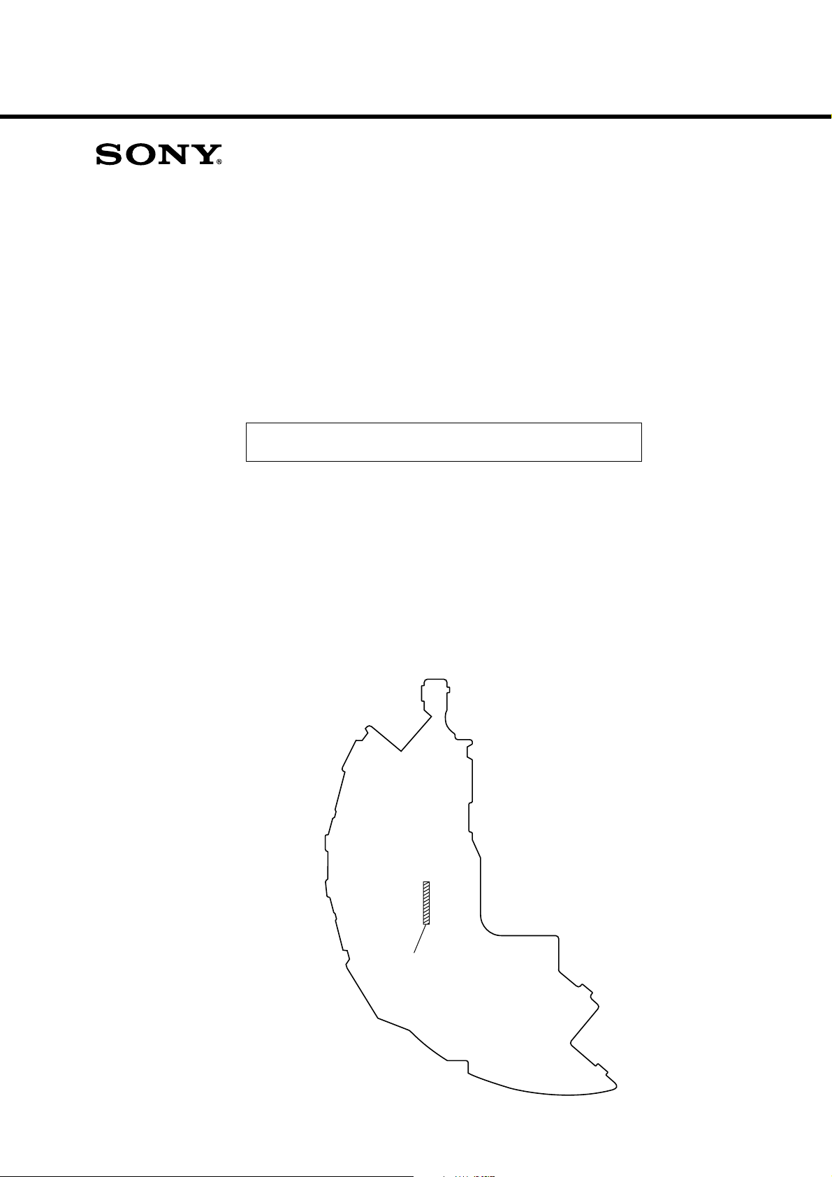
• NEW/FORMER TYPE DISCRIMINATION
– MAIN BOARD (Component Side) –
Chinese Model
Tourist Model
Former Type: 1-682-611-11
New Type : 1-682-611-12

D-EJ955
• DIAGRAMS
NOTE FOR PRINTED WIRING BOARDS AND SCHEMATIC DIAGRAMS
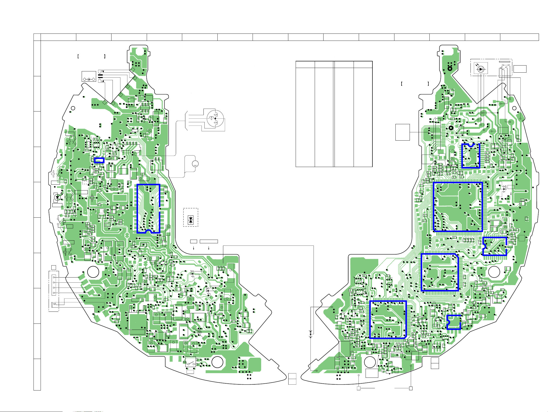
Note on Printed Wiring Board
• X : parts extracted from the component side.
• Y : parts extracted from the conductor side.
z
•
• : Pattern from the side which enables seeing.
(The other layers' patterns are not indicated.)
Caution:
Pattern face side: Parts on the pattern face side seen from
(Conductor Side) the pattern face are indicated.
Parts face side: Parts on the parts face side seen from
(Component Side) the parts face are indicated.
• MAIN board is multi-layer printed board. Howe ver , the patterns
: Through hole.
of intermediate-layer have not been included in the diagram.
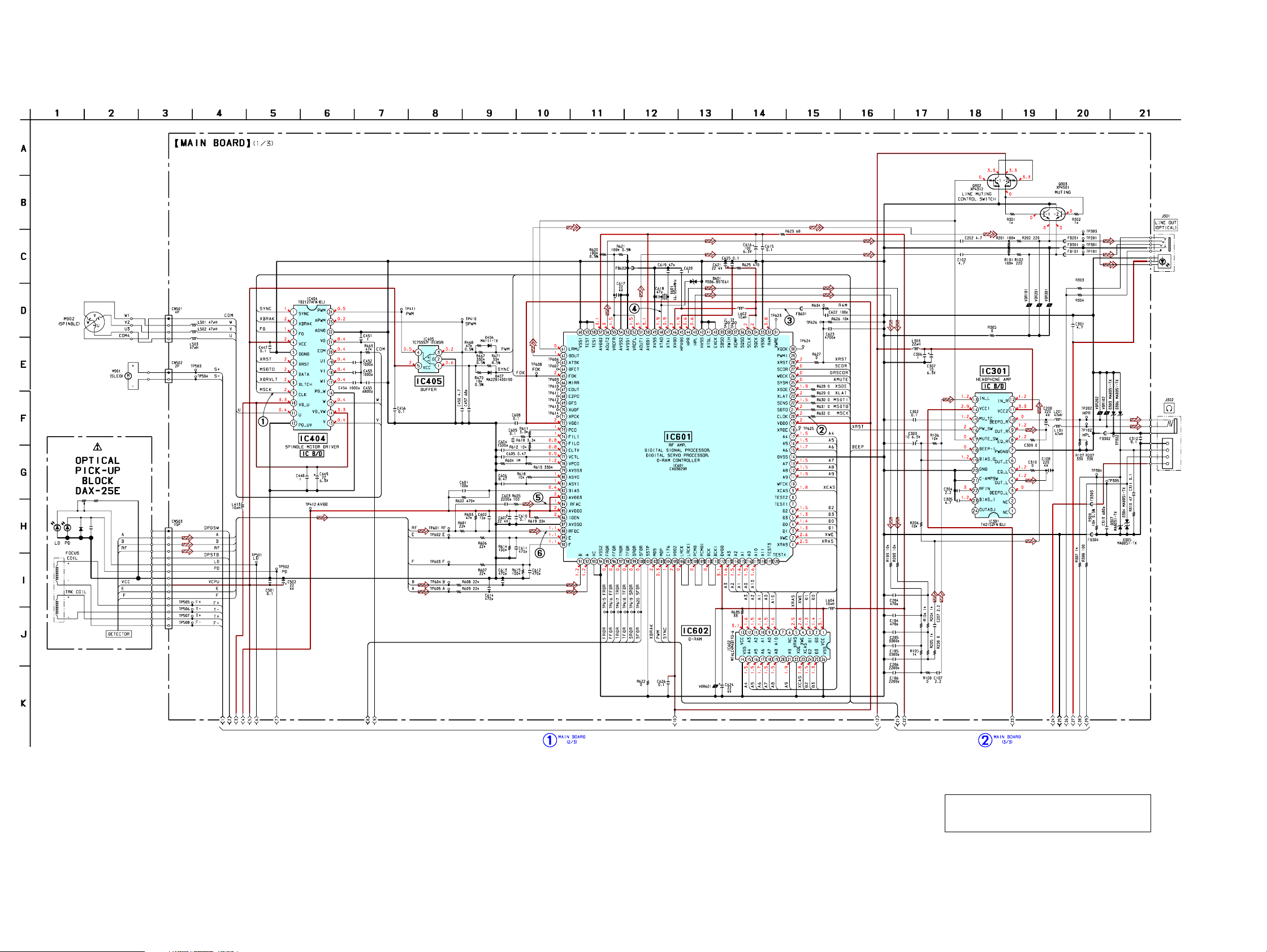
Note on Schematic Diagram:
• All capacitors are in µF unless otherwise noted. pF: µµF
50 WV or less are not indicated except for electrolytics
and tantalums.
• All resistors are in Ω and 1/
specified.
• % : indicates tolerance.
• C : panel designation.
Note: The components identified by mark 0 or dotted line
with mark 0 are critical for safety.
Replace only with part number specified.
• A : B+ Line.
• Power v oltage is dc 4.5 V and fed with regulated dc power
supply from DC IN jack (J401).
• Voltages and w av eforms are dc with respect to ground in
no-signal conditions.
no mark : CD PLAY
• Voltages are tak en with a V OM (Input impedance 10 MΩ).
Voltage var iations may be noted due to normal production tolerances.
• Waveforms are taken with a oscilloscope.
Voltage var iations may be noted due to normal production tolerances.
• Circled numbers refer to waveforms.
• Signal path.
J : CD PLAY (ANALOG OUT)
c : CD PLAY (OPTICAL OUT)
• Abbreviation
FR : French model
4
W or less unless otherwise
2

PRINTED WIRING BOARD
1 2 3 4 5 6 7 8 9 10 11 12 13 14
D-EJ955
A
B
MAIN BOARD
(COMPONENT SIDE)
J401
EXT BATT
DC IN 4.5V
+
–
TH401
FB401
6
4
Q412
1
3
B
Q414
+
IC602
VDR801
FB801
R458
R801
R802
C
E
C607
+
C
C501
C610
C440
C401
+
C805
C804
C426
R479
C502
+
C807
R808
C464
+
FB402
12
CN502
L604
C806
C810
C811
+
R474
+
C444
L403
C425
L405
13
1
D803
A
R813
VDR403
A
K
SL806
(OPEN)
D805
R635
+
C624
VDR601
C808
R811
R435
L410
R439
+
C432
R477
R478
Q303
1E
1B
2C
R301
IC405
D407
R821
(FR)
R822
S805
x/CHARGE
R814
C104
C106
C307
C456
R103
C107
+
C812
D601
L303
1C
2B
2E
X601
C306
2E
3
R471
AK
R470
C617
C625
R104
C105
R105
R108
R106
R206
C309
R302
C618
C621
2B
Q302
4
1C
2C
+
R620
C619
FB601
C310
1B
5
1
+
R625
R634
R467
C457
R621
C108
R623
R626
1
CN501
R804
Q301
C608
R805
BCE
4
L413
14
26
1E
C447
D406
K
A
R468
C450
C451
L501
L503
L502
C615
C616
+
C620
L602
FB602
C622
C623
+
+
C208
D804
L101
L201
C801
C802
AK
D408
EB
FB302
C312
Q405
C
S808
VOL +
D
R819
S809
VOL –
D801
E
CHARGE
R816
R818
C814
R815
R817
S807
.
F
J302
S806
> N
i
G
H
I
J
C809
SL807
(TEST)
FB803
R807
L401
R812
L411
4
1
2
RED
1
BLK
D601,
D804, 805
S802
FB405
FB404
C446
+
+
C466
S804
OPEN
S802
AVLS
LIMIT
NORM
+
C433
BLK
ORG
WHT
RED
C422
+
V
U
W
M902
(SPINDLE)
M901
M
(SLED)
S803
G
•
PROTECTION
2
1
C408
R417
+
R418
C411
L408
L409
S803
C419
L402
L404
L406
+
C412
C424
C413
+
R413
R437
R416
R444
R421
1-682-611-
• Semiconductor Location
D303 H-13
D304 H-13
D305 H-13
D306 H-13
D307 H-13
D401 J-9
D403 B-12
D404 I-11
D405 I-11
D406 C-3
D407 D-2
D408 H-3
D601 E-2
D801 E-1
D803 G-4
D804 G-3
D805 G-4
IC301 F-13
IC402 I-12
IC403 H-10
IC404 D-13
R484
4
RECHARGEABLE
BATTERY
NC-6WM
2PSC. 2.4V
12
(12)
6
D401
Ref. No. LocationRef. No. Location
IC405 D-2
IC601 E-12
IC602 E-4
IC801 G-12
Q301 C-3
Q302 C-2
Q303 C-2
Q403 H-9
Q405 H-3
Q406 H-12
Q407 J-10
Q412 B-3
Q414 C-3
Q415 H-9
Q416 I-9
Q417 H-9
Q418 H-10
Q419 G-9
Q420 G-10
Q421 I-12
Q422 I-12
1E
2C
1B
Q419
1C
R491
R493
R490
1E
B
E
Q403
C
Q417
BE
SDG
C
Q415
3
R483
R432
1
R443
C417
C409
R442
R422
C421
R445
C423
R423
R426
– +CHARGE TEMINAL
Q416
R420
C418
R436
AK
C405
2B
R419
C414
R441
1B
2E
2C
R440
2E
R485
41
C416
60
R424
R457
C429
R486
2B
Q418
J301
LINE OUT
TP418
(GND)
(OPTICAL)
MAIN BOARD
(CONDUCTOR SIDE)
D403
OPTICAL
PICK-UP
BLOCK
DAX-25E
R602
C601
R601
R603
C603
R606
R614
C602
20
R609
C612
120
91
C611
R619
1
C613
R615
R607
R608
C614
C626
R622
21
IC801
R487
1E
2C
Q407
R447
R448
R425
BCE
Q420
2E
D404
VDR401
1B
2B
1C
21
80
AK
20
1
R449
R463
D405
R454
C439
R450
C436
C465
C437
40
KA
C438
41
C445
R465
R460
R461
R455
C434
1-682-611-
C442
C431
Q406
C443
C406
R414
C469
Q421
12
R409
B
C468
Q422
3
4
C
(12)
1C
40
IC403
61
R446
R459
C435
R429
R452
R456
CN503
15
E
1
6
1
R604
2B
2C
C604
R605
R482
R415
E
C404
KA
R305
R410
TP601
(RF)
C449
+
C448
C605
C606
R612
R613
R618
IC601
1
60
R401
8
1
1B
IC402
1C
R488
R489
R632
12
C609
5
4
1
80
61
C301
IC404
R610
R611
R631
C803
R806
VDR202
C403
R630
D307
R428
R629
R628
R820
R307
R107
D303
R207
KA
R627
R310
FB201
VDR201
VDR301
R303
C313
C202
S801
HOLD
HOLD
OFF
C303
C204
C207
FB301
R202
R203
R201
C205
R208
R204
R304
R803
C206
VDR803
R492
R205
24
13
6190
30
VDR101
FB101
R469
R101
C452
R102
C453
C454
C102
C455
60
C305
C304
C302
+
13
31
24
IC301
AK
1
R309
VDR102
C311
AK
D306
FB403
FB304
R308
KA
D305
12
FB303
KA
D304
33

D-EJ955
SCHEMATIC DIAGRAM – MAIN Board (1/3) –
∗ R303, 304
220k (FR)
330k (EXCEPT FR)
∗
∗
(Page 5)
(Page 6)
The components identified by mark 0 or dotted
line with mark 0 are critical for safety.
Replace only with part number specified.
44
 Loading...