

Sony DEJ-955 Service manual
D-EJ955
SERVICE MANUAL
Ver 1.2 2002.09
SPECIFICATIONS
AEP Model
UK Model
E Model
Australian Model
Chinese Model
Tourist Model
Model Name Using Similar Mechanism NEW
CD Mechanism Type CDM-3325ES
Optical Pick-up Name DAX-25E
System
Compact disc digital audio system
Laser diode properties
Material: GaAlAs
Wavelength: λ = 780 nm
Emission duration: Continuous
Laser output: Less than 44.6 µW
(This output is the value measured at a distance
of 200 mm from the objective lens surf ace on
the optical pick-up block with 7 mm aperture.)
D-A conversion
1-bit quartz time-axis control
Frequency response
20 - 20 000 Hz
307)
Output (at 4.5 V input level)
Line output (stereo minijack)
Output level 0.7 V rms at 47 kΩ
Recommended load impedance over 10 kΩ
Headphones (stereo minijack)
Appro x. 5 mW + Appro x. 5 mW at 16 Ω
(Approx. 0.5 mW + Approx. 0.5 mW
at 16 Ω)*
*For the customers in Fr ance
Optical digital output (optical output connector)
Output level: –21 - –15 dBm
Wavelength: 630 - 690 nm at peak level
Power requirements
For the area code of the model you
purchased, check the upper left side of the
bar code on the package.
• Two Son y NC-6WM rechargeable batteries:
2.4 V DC
• Two LR6 (size AA) ba tteries: 3 V DC
+1
dB (measured by JEIT A CP-
–2
• AC power adaptor (DC IN 4.5 V jack):
AEP, French, East European, E13 models:
220 - 230 V, 50/60 Hz
UK model: 230 - 240 V, 50 Hz
Australian model : 240 V, 50 Hz
E33, Korean, Tourist models:
100 - 240 V, 50/60 Hz
Hong Kong model: 220 V, 50/60 Hz
Chinese model: 220 V , 50 Hz
Battery life* (appr o x. hour s)
(When you use the CD player on a flat and stable
surface.)
Playing time va ries de pending on ho w the CD
player is used.
When using G-PROTECTION
“1” “ 2”
Two NC-6WM 19 19.5
(charged for
about 5 hours**)
External battery case 66 71
(two alkaline ba tteries***)
Rechargeable batteries 88 92
NC-6WM and
e xternal battery case
(two alkaline ba tteries***)
* Measured value by the standard of JEITA
(Japan Electronics and Informa tion Technology
Industries Association).
** Charging time varies depending on how the
rechargeable battery is used.
*** When using Sony alkaline batteries LR6 (SG)
(produced in Japan)
Operating temperature
5°C - 35°C (41°F - 95°F)
Dimensions (w/h/d) (excluding
projecting parts and controls)
Approx. 135.0 × 135.0 × 15.9 mm
3
3
(5
⁄8 × 5
⁄8 × 21⁄32 in.)
Mass (excluding accessories)
Approx. 166 g (5.9 oz)
Supplied accessories
For the area code of the location in which you
purchased the CD player, check the upper left side
of the bar code on the package.
AC power adaptor (1)
Headphones/earphones with remote control (1)
Rechargeable batteries (2)
Charging stand (1)
Battery carrying case (2)
Carrying pouch (1)
External battery case (1)
AC plug adaptor (1)*
* Supplied with E33 and tourist models
Design and specif ications are subject to change
without notice.
• Abbreviation
E13: 220 - 230 V AC area in E model
E33: 100 - 240 V AC area in E model
PORTABLE CD PLAYER
9-873-376-03 Sony Corporation
2002I0500-1 Personal Audio Company
C 2002.09 Published by Sony Engineering Corporation

D-EJ955
TABLE OF CONTENTS
1. SERVICING NOTES............................................... 3
2. GENERAL ................................................................... 6
3. DISASSEMBLY
3-1. Disassembly Flow ........................................................... 7
3-2. Upper Lid (A) Sub Assy ................................................. 7
3-3. Cabinet (Upper) Sub Assy .............................................. 8
3-4. Main Board, Optical Pick-up Section
(CDM-3325ES) ............................................................... 8
4. ELECTRICAL CHECK .......................................... 9
5. DIAGRAMS
5-1. Block Diagram – MAIN Section (1/2) – ....................... 10
5-2. Block Diagram – MAIN Section (2/2) – ....................... 11
5-3. Block Diagram – POWER SUPPLY Section – ............. 12
5-4. Note for Printed Wiring Boards and
Schematic Diagrams ....................................................... 13
5-5. Printed W iring Board ...................................................... 14
5-6. Schematic Diagram – MAIN Board (1/3) – .................. 15
5-7. Schematic Diagram – MAIN Board (2/3) – .................. 16
5-8. Schematic Diagram – MAIN Board (3/3) – .................. 17
5-9. IC Pin Function Description ........................................... 18
6. EXPLODED VIEWS
6-1. Upper Lid, Cabinet (Upper) Section .............................. 25
6-2. Cabinet (Lower) Section................................................. 26
6-3. Optical Pick-up Section (CDM-3325ES)....................... 27
On AC power adaptor
• Use only the AC power adaptor supplied or
recommended in “Accessories (supplied/
optional).” Do not use any other AC power
adaptor. It may cause a malfunction.
Polarity of the plug
Notes on chip component replacement
• Never reuse a disconnected chip component.
• Notice that the minus side of a tantalum capacitor may be dam-
aged by heat.
Flexible Circuit Board Repairing
• Keep the temperature of the soldering iron around 270 ˚C during repairing.
• Do not touch the soldering iron on the same conductor of the
circuit board (within 3 times).
• Be careful not to apply force on the conductor when soldering
or unsoldering.
CAUTION
Use of controls or adjustments or performance of procedures
other than those specified herein may result in hazardous radiation exposure.
This appliance is classified as a CLASS 1 LASER product.
The CLASS 1 LASER PRODUCT MARKING is located on
the rear exterior.
7. ELECTRICAL PARTS LIST ............................... 28
SAFETY-RELATED COMPONENT WARNING!!
COMPONENTS IDENTIFIED BY MARK 0 OR DOTTED
LINE WITH MARK 0 ON THE SCHEMATIC DIAGRAMS
AND IN THE PARTS LIST ARE CRITICAL TO SAFE
OPERATION. REPLACE THESE COMPONENTS WITH
SONY PARTS WHOSE PART NUMBERS APPEAR AS
SHOWN IN THIS MANU AL OR IN SUPPLEMENTS PUBLISHED BY SONY.
2
SECTION 1
SERVICING NOTES
D-EJ955
About CD-Rs/CD-RWs
This CD player can play CD-Rs/CD-RWs recorded in the CD-D A
format*, but playback capability may vary depending on the quality of the disc and the condition of the recording device.
* CD-DA is the abbreviation for Compact Disc Dig ital Audio. It is
a recording standard used for the Audio CDs.
NOTES ON HANDLING THE OPTICAL PICK-UP
BLOCK OR BASE UNIT
The laser diode in the optical pick-up block may suffer electrostatic breakdown because of the potential difference generated by
the charged electrostatic load, etc. on clothing and the human body .
During repair, pay attention to electrostatic breakdown and also
use the procedure in the printed matter which is included in the
repair parts.
The flexible board is easily damaged and should be handled with
care.
NOTES ON LASER DIODE EMISSION CHECK
The laser beam on this model is concentrated so as to be focused
on the disc reflective surface by the objective lens in the optical
pick-up block. Therefore, when checking the laser diode emission, observe from more than 30 cm away from the objecti ve lens.
BEFORE REPLACING THE OPTICAL PICK-UP BLOCK
Please be sure to check thoroughly the parameters as par the “Optical Pick-Up Block Checking Procedures” (Part No.: 9-960-027-
11) issued separately before replacing the optical pick-up block.
Note and specifications required to check are given below.
• FOK output: IC601 yg pin
When checking FOK, remove the lead wire to disc motor.
• RF signal P-to-P value: 0.4 to 0.6 Vp-p
LASER DIODE AND FOCUS SEARCH OPERATION
CHECK
During normal operation of the equipment, emission of the laser
diode is prohibited unless the upper lid is closed while turning ON
the S804. (push switch type)
The following checking method for the laser diode is operable.
• Method:
Emission of the laser diode is visually checked.
1. Open the upper lid.
2. With a disc not set, turn on the S801 with a screwdri ver having
a thin tip as shown in Fig.1.
3. Press the
4. Observing the objective lens, check that the laser diode emits
light.
When the laser diode does not emit light, automatic power
control circuit or optical pickup is faulty.
In this operation, the objective lens will move up and down 4
times along with inward motion for the focus search.
> N button.
S804
detection lever
detection lever
MAIN board
Fig. 1 Method to push the S804
3
D-EJ955
SERVICE MODE
In the Service mode, this set can check the following.
1. Service Mode Setting Method
To set the service mode, perform as follows.
1) Make sure that the power is not turned on.
2) Check for the following states:
Open/close detection switch (S804)......OFF
Solder bridge at SL806 (OPEN)............ OPEN
[AVLS] switch (S802) ........................... NORM
[HOLD] switch (S801) .......................... OFF
•
[G PROTECTION] switch (S803) ....... 1
3) Short the solder bridge at the SL807 (TEST) on the MAIN
board (see Fig. 2).
4) Turn the power on.
– MAIN Board (Component Side) –
R811
D803
C809
R807
SL807
(TEST)
R812
FB803
VDR8
C805
+
C440
+
C806
C807
C804
C464
SL806
(OPEN)
R808
C810
A
C811
K
A
D805
R813
2. Operation in Service Mode
When the Service mode is set, the LCD on the remote commander
displays the following.
Remote commander LCD display
Microcomputer
version display
All lit
Service mode
VD101
888
DDDD
BASS12
3. Operation of Buttons and Knobs in Service Mode
The following operation can be checked by operating the buttons
and knobs on the set and remote commander.
3-1 . Case without Setting a CD
> N / . buttons on the set and > N / . knobs on
•
remote commander
Optical pick-up movement (outward or inward)
Tracking/sled servo off
Note: Do not look directly at the laser beam from the optical pick-up.
Do not move forcibly the optical pick-up exceeding the most-outside or most-inside track.
3-2 . Case with Setting a CD
Cheking method:
1) Make sure that the power is not turned on.
2) Leave a solder bridge of the SL807 (TEST) on the MAIN board
shorted.
3) Turn the power on, and then set a CD and play it with the X
button on the remote commander.
Fig. 2
Remote Commander LCD display
0000
(play mode)
• x button on the set and remote commander
All servos (focus/tracking/sled) off
• > N / . buttons on the set and > N / . knobs on
remote commander
Optical pick-up movement (outward or inward)
Tracking/sled servo off
• [PRT/ENT] button on remote commander
Tracking gain up mode
Remote Commander LCD display
Up0000
(For the rest, turn the power off and then turn it on again)
• [VOL +] / [VOL --] buttons on the set and [VOL +] / [VOL --]
knobs on remote commander
2-step volume setting
• [PLAYMODE] button on remote commander
CL V speed becomes 1 to 4 times each time the button is pr essed
Tracking/sled servo on
4

Remote Commander LCD display
D-EJ955
010001
040004
(For the rest, turn the power off and then turn it on again)
• [SOUND] button on remote commander
Servo auto adjustment
4.Service Mode Releasing Method
To release the service mode, perform as follows.
1) Turn the power off.
2) Open the solder bridge at the SL807 (TEST) on the MAIN
board.
Note: Remove the solder completely.
5.Error Rate Check Display
The C1 error rate check display mode becomes active if the following operation is performed during the operation in the normal
mode.
1) Turn the power off, and cancel other service operations.
2) Turn the power on, and then set a CD and play it with the X
button on the remote commander.
Remote Commander LCD display
(1 time)
(4 times)
0000
3) Press the [SOUND] button on the remote commander to make
automatic adjustment.
4) Press the [PLAY MODE] button on the remote commander.
Remote Commander LCD display
010001
5) Press the [DISPLAY] button on the remote commander, and
the C1 error rate display will be activated and the LCD on the
remote commander will display as follows.
Remote Commander LCD display
Er****
Note: In the play state, press the [SOUND] button on the remote com-
mander before pressing the [PLAY MODE] b utton. Wrong order of
button operations will result in very large Er**** value.
6) Turn the power off.
7) Open the solder bridges at the SL807 (TEST) on the MAIN
board.
Note: Remove the solder completely.
**** value
0000 to 0099 : OK
more than 0100 : NG
5

D-EJ955
SECTION 2
GENERAL
This section is extracted from
instruction manual.
Getting started
Locating the controls
For details, see pages in parentheses.
CD player (front)
1 EXT BATT (external battery)/
DC IN 4.5 V (external power
input) jack (pages 7, 20, 22)
2 LINE OUT (OPTICAL) jack
(page 17)
3 VOL (volume) +*/– buttons
(page 8)
4 x (stop) /CHARGE button•
CHARGE lamp
(pages 8, 15, 16, 19, 20)
5 .(AMS/search)•> N*
(AMS/search/play) buttons
(pages 7, 8, 12)
6 i (headphones) jack
(page 7)
7 OPEN switch
(page 7)
8 Terminals for the charging stand
(pages 19, 25)
CD player (inside)
9 AVLS switch
(page 15)
q; G-PROTECTION
switch
(page 13)
qa Battery
compartment
*The button has a tactile dot to help you operate the CD player by touch.
4
(page 19)
CD player (rear)
qs HOLD switch
(page 15)
Remote control
qd Display
(pages 9, 11 - 15)
qf Rotary control
N/>: play, AMS/search (pages 8, 12)
.: AMS/search (pages 8, 12)
VOL +/–: Pull the control in the direction of the
arrow, and then turn it toward + or –. (page 8)
qh Clip
qj DISPLAY
button
(pages 13, 14)
qk PLAY MODE
button
(pages 10 - 12, 16)
ql RPT (repeat)/ENT
(enter) button
(pages 10 - 12)
qg x (stop) button
(pages 8, 16)
w; HOLD switch
(page 15)
wa i (headphones) jack
(page 7)
ws X (pause) button
(page 8)
wd SOUND button
(page 14)
Note
Use only the supplied remote control. You cannot
operate this CD player with the remote control
supplied with other CD players.
Getting started
5
Using the carrying pouch
You can carry your player and its battery case together using the supplied carrying pouch. Insert
them into the proper places in the pouch as illustrated below.
6
6

• This set can be disassembled in the order shown below.
3-1. DISASSEMBLY FLOW
3-2. UPPER LID (A) SUB ASSY
3-3. CABINET (UPPER) SUB ASSY
3-4. MAIN BOARD,
SECTION 3
DISASSEMBLY
SET
(Page 7)
(Page 8)
OPTICAL PICK-UP SECTION (CDM-3325ES)
(Page 8)
D-EJ955
Ver 1.1
Note: Follow the disassembly procedure in the numerical order given.
3-2. UPPER LID (A) SUB ASSY
3
guide (L)
5
guide (R)
2
screw (M1.4)
!
@
1
Open the upper lid (A) sub assy.
Note: To install screws, tighten them with 0.4kg/cm2 of torque.
(If tighten them too hard, portion
4
screw (M1.4)
!
may get cracked.)
6
Remove the upper lid (A)
sub assy in the direction of
arrow
A
.
A
7

D-EJ955
n
3-3. CABINET (UPPER) SUB ASSY
2
four screws (B2)
knob (GPRO)
3
claw
1
screw (B2)
4
cabinet (upper) sub assy
3
claw
2
three screws (B2)
3
claw
5
battery terminal board
(relay)
6
spring (upper lid-2702)
S802
S803
Note : On installation of cabinet (upper) sub assy,
adjust the position of two switches (S802, S803)
and two knobs (GPRO).
3-4. MAIN BOARD, OPTICAL PICK-UP SECTION (CDM-3325ES)
1
cushion
2
two connectors
(CN501, CN502)
7
two insulators
6
main board
1
cushion
8
optical pick-up section
(CDM-3325ES)
5
flexible board
(CN503)
7
insulator
3
Hold up both the main board and the optical
pick-up section at once, and remove them
form the cabinet (lower) assy.
4
cabinet (lower) assy
Note : Handle the flexible board with care whe
you hold up the optical pick-up section.
8

SECTION 4
p
ELECTRICAL CHECK
D-EJ955
The CD section adjustments are done automatically in this set.
In case of operation check, confirm that focus bias.
Precautions for Check
1. Perform check in the order given.
2. Use YEDS-18 disc (P art No.: 3-702-101-01) unless otherwise
indicated.
3. Power supply voltage requirement: DC4.5 V in DC IN jack.
(J401)
VOLUME : Minimum
AVLS switch : NORM
HOLD switch : OFF
G•PROTECTION switch : 1
Connecting and Checking Location:
– MAIN Board (Component Side) –
TP418
(GND)
J301
LINE OUT
(OPTICAL)
TP601 (RF)
Focus bias Check
Condition:
• Hold the set in horizontal state.
Connection:
MAIN board
TP601 (RF)
TP418 (GND)
2 k
Ω
oscilloscope
(AC range)
+
–
Procedure:
1. Connect the oscilloscope to the test points TP601 (RF) and
TP418 (GND) on the MAIN board.
2. Set a disc. (YEDS-18)
3. Press the > N button.
4. Check the oscilloscope waveform is as shown below.
A good eye pattern means that the diamond shape (◊) in the
center of the waveform can be clearly distinguished.
RF Signal reference Waveform (Eye Pattern)
VOLT/DIV : 100 mV (With the 10:1 probe in use)
TIME/DIV : 500 ns
OPTICAL
PICK-UP
BLOCK
DAX-25E
R601
R603
R602
C601
C603
D403
CN503
1
15
R604
KA
R410
C604
C448
606
605
R305
C404
C449
+
R489
1
12
VDR304
C301
IC404
VDR303
RF level
0.4 to 0.6 Vp-
To watch the eye pattern, set the oscilloscope to AC range and
FB201
VDR201
VDR301
R303
C202
FB301
R202
R304
R201
VDR101
24
FB101
R469
R101
C452
C453
C102
C454
13
R102
55
increase the vertical sensitivity of the oscilloscope for easy watching.
5. Stop revolving of the disc motor by pressing the x button.
99

D-EJ955
SECTION 5
DIAGRAMS
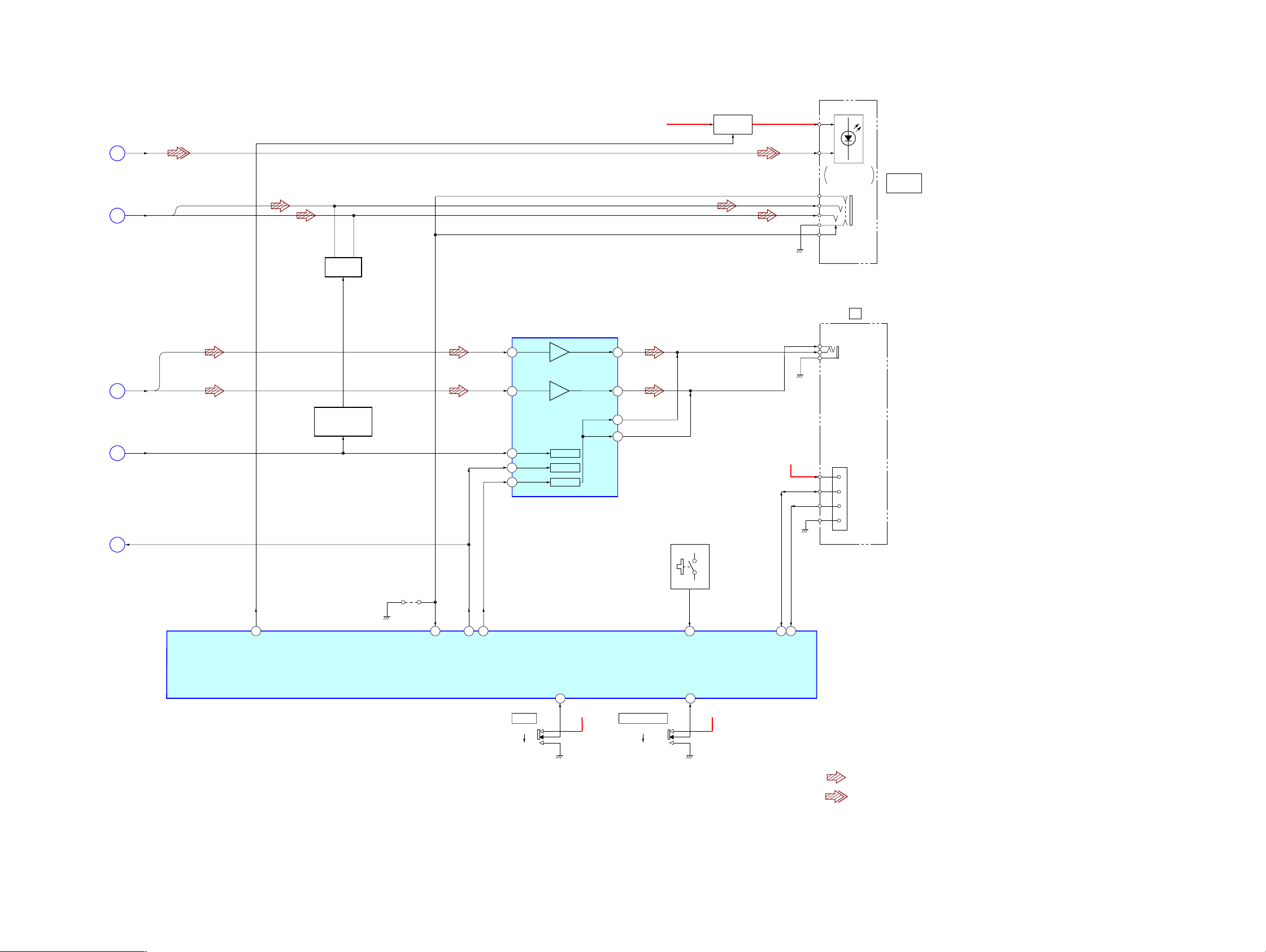
5-1. BLOCK DIAGRAM – MAIN Section (1/2) –
DETECTOR
A
(Page 12)
B
(Page 12)
C
(Page 12)
OPTICAL PICK-UP BLOCK
LASER DIODE
PD
LD
(FOCUS)
2-AXIS
DEVICE
(TRACKING)
M902
(SPINDLE)
V
U
W
VG
• SIGNAL PATH
: CD PLAY (ANALOG OUT)
: CD PLAY (OPTICAL OUT)
A
B
RF
E
F
VCC
DAX-25E
PD
OPSTB
OPGSW
LD
A
B
RF
E
F
VCPU B+
M901
M
(SLED)
U1
19
18
17
20
11
13
15
21
V1
W1
COM
U
V
W
VG
+
+
+
PREDRIVER
FOCUS/TRACKING COIL DRIVER
SLED MOTOR DRIVER
IC403 (1/2)
FO2
34
RO2
32
FO1
38
36
26
24
CONTROLLER,
RO1
H BRIDGE DRIVER
FO4
RO4
SPINDLE MOTOR DRIVER
IC404
CONTROL
CIRCUIT
RI2
RI1
RF AMP,
DIGITAL SIGNAL PROCESSOR,
DIGITAL SERVO PROCESSOR,
D-RAM CONTROLLER
IC601
A
92
B
91
RFDC
88
RFAC
81
E
89
F
90
FI2
17
18
FI1
40
41
FI4
21
FI4
22
SYNC
1
CPU
INTERFACE
XRST
6
PWM
APWM
XBRAK
DATA
CLK
XLTCH
24
23
2
FG
3
7
9
8
BUFFER
IC405
100
99
96
95
98
97
104
103
102
72
74
77
78
SFDR
SRDR
FFDR
FRDR
TFDR
TRDR
C176
MDP
MDS
FG/FGSEL
XDRVLT
HG XSTB
HG GUP
S801
HOLD
HOLD
OFF
SCOR
27
40
SCOR
HOLD
VCPU B+
WDCK
WFCK
MDS
XTAO
XTAI
RFAC
MDP
XSOE
SENS
R4M
XLAT
CLOK
SCOR
SDTO
RFDC
SFDR
SRDR
FFDR
FRDR
TFDR
TRDR
SL806
(OPEN)
E
F
B
A
SIGNAL
PROCESSOR
BLOCK
SDTD
SENS
CLOK
161415181711
MSDTI
MSDTO
CLOSE
28
XLAT
MSCK
S804
OPEN
D-RAM
IC602
DOUT
AOUTL,
AOUTR
HPL,
HPR
LRMU
XRST
SYNC
D
E
F
G
H
J
(Page 11)
(Page 11)
(Page 11)
(Page 11)
(Page11)
(Page 12)
SYSM
25
13
AMUTE
DOUT
62
D0-D3
4, 3, 6, 5
A0-A10
116 – 113, 17 – 15, 13 – 11, 117
XRAS
1
XWE
2
XCAS
9
XTAI
47
XTAO
48
AOUT1
51
AOUT2
56
HPL
43
HPR
44
LRMU
61
XRST
28
D1 – D4A0 – A10
2, 3, 24, 25
9 – 12, 15 – 19, 21, 8
5
XRAS
4
XWE
23
XCAS
X601
16.9344MHz
DIGITAL
OUT
MEMORY
CONTROLLER,
BUS BOOST
BLOCK
LPF
SERVO
BLOCK
R4M
XSOE
WDCK
242232232021
26
2
12
XIN
XLAT
XSOE
GRSCOR
SYSTEM CONTROLLER
VCPU B+
FOK
FOK
65
9
FOK
IC801 (1/3)
SCK
SDTO
K
L
(Page 12)
(Page 12)
1010
5-2. BLOCK DIAGRAM – MAIN Section (2/2) –
D-EJ955
(Page 10)
(Page 10)
(Page 10)
(Page 10)
(Page 10)
VCC3
DOUT
D
AOUTL
HPL
HPR
AOUTR
MUTING
Q303
LINE MUTING
CONTROL SWITCH
Q302
13
12
17
18
15
MUTE_SW
HEADPHONE AMP
IN_L
IN_R
PW_SW
BEEP
IC301
MUTE SW
PW SW
BEEP
OUT_L
OUT_R
BEEPO_L
BEEPO_R
4
9
3
10
S805-809
E
F
LRMU
G
XRST
H
B+ SWITCH
Q301
VCPU B+
OPTICAL
TRANSCEIVER
(LINE OUT JACK)
J302
i
VCPU 2V
4
3
TSB
2
RMKEY
GND
1
J301
LINE OUT
(OPTICAL)
SL807
(TEST)
6 24 79 30 2625
P21
SYSTEM CONTROLLER
IC801(2/3)
AD SEL
XRST
BEEP
S802
AVLS
LIMIT
NORM
39
AVLS
VCPU B+
S803
G•PROTECTION
2
1
AD KEY
ESP
38
31
TSB
AD RMKEY
VCPU B+
• SIGNAL PATH
: CD PLAY (ANALOG OUT)
: CD PLAY (OPTICAL OUT)
1111

D-EJ955
5-3. BLOCK DIAGRAM – POWER SUPPLY Section –
(Page 10)
(Page 10)
(Page 10)
(Page 10)
(Page 10)
(Page 10)
VG
C
PD
A
SYNC
J
SDTO
L
SCK
K
LD
B
SYSTEM CONTROLLER
IC801 (3/3)
AD CHGMNT
XPOWLT
XWAKE
RESET
LEDDISP
PPG
AGCPWN
POWER CONTROL
IC403 (2/2)
PAPC
3
SYNC
11
DATA
14
CLOCK
13
VLGO4
69
INM4
6
RF4
5
RF41
2
75
66
8
80
29
70
NC
10
21
D801
CHARGE
VCC1
VCPU B+
VCC2
B+ SWITCH
Q418
SWITCHING
Q419
SWITCHING
Q420
VCC3
15
12
16
51
56
61
50
57
75
74
73
78
7
53
79
1
49
58
LATCH
WAKE
RSTB
VCC1
INP2
VLGO2
VCPU
STNG
VCC3
VCC2
VLGO3
RF3
APCREF
DTC2
DTC3
VREF
VDRAM
CHGMNT
VREF
CHGSW
RF1
INM1
RS1
VIN
DTC3
INP2
VCC1
VCC2
VCC3
VCPU
WAKE
LATCH
DATA
CLOCK
RF41
RF4
INM4
APCREF
PAPC
DTC2
LINEAR
CONSTANT CURRENT,
CONSTANT VOLTAGE
CHARGING BATTERY
CHARGE CIRCUIT
SWITCHING
POWER
CIRCUIT
SWITCHING
POWER
CIRCUIT
LINEAR
REGULATOR
INTERFACE
CLK
OR OSC
SAW
GEN.
CHARGING BATTERY
VOLTAGE DETECTOR
CIRCUIT
PRE-DRIVER
VG
POWER
CIRCUIT
VLGO4
VLGO2
VLG3
VG
L5
BATM1
BATM2
CHGMNT
DC IN
BATM1
BATM2
RF1
INM1
DCIN
RS1
CHGSW
VIN
Q421, 422
VIN B+
CHARGE
CHARGE ON
SWITCH
Q412
B+ SWITCH
Q416, 417
+
–
RECHARGEABLE
BATTERY
NC-6WM
2PCS. 2.4V
J401
EXT BATT
DC IN 4.5V
–
CHARGE
TERMINAL
+
VG
9
L5
8
60
59
46
45
48
43
42
65
CHARGE
CONTROL
Q406, 415
B+ SWITCH
IC402
CHARGE ON
SWITCH
Q403
D405
RIPPLE
FILTER
Q408
D403
D404
B+ SWITCH
AD DCINMNT
EXTBATT
AD BATMNT
CHGGND ON
BATVCC ON
XSTAND ON
27
33
22
76
7
37
EXTERNAL BATTERY
DETECT
Q407
CHARGE STAND
DETECT
Q407
1212

D-EJ955
400 to 600
mVp-p
2.0 Vp-p
950 ns
5-4. NOTE FOR PRINTED WIRING BOARDS AND SCHEMATIC DIAGRAMS
Note on Printed Wiring Board
• X : parts extracted from the component side.
• Y : parts extracted from the conductor side.
z
•
• : Pattern from the side which enables seeing.
(The other layers' patterns are not indicated.)
Caution:
Pattern face side: Parts on the pattern face side seen from
(Conductor Side) the pattern face are indicated.
Parts face side: Parts on the parts face side seen from
(Component Side) the parts face are indicated.
• MAIN board is multi-layer printed board. Howev er , the patterns
: Through hole.
of intermediate-layer have not been included in the diagram.
Note on Schematic Diagram:
• All capacitors are in µF unless otherwise noted. pF: µµF
50 WV or less are not indicated except for electrolytics
and tantalums.
• All resistors are in Ω and 1/
specified.
• % : indicates tolerance.
• C : panel designation.
Note: The components identified by mark 0 or dotted line
with mark 0 are critical for safety.
Replace only with part number specified.
• A : B+ Line.
• Pow er voltage is dc 4.5 V and fed with regulated dc power
supply from DC IN jack (J401).
• V oltages and wa vef orms are dc with respect to ground in
no-signal conditions.
no mark : CD PLAY
• V oltages are taken with a VOM (Input impedance 10 MΩ).
Voltage variations may be noted due to normal production tolerances.
• Waveforms are taken with a oscilloscope.
Voltage variations may be noted due to normal production tolerances.
• Circled numbers refer to waveforms.
• Signal path.
J : CD PLAY (ANALOG OUT)
c : CD PLAY (OPTICAL OUT)
4
W or less unless otherwise
• Waveforms
1 IC404 9 (CLK)
950 ns
2 IC601 w; (CLOK)
950 ns
2.0 Vp-p
2.0 Vp-p
6 IC601 ik (RFDC) (CD play mode)
7 IC403 qd (CLOK)
2.0 Vp-p
950 ns
3 IC601 es (R4M)
236 ns
4 IC601 rk (XTAO)
59.1 ns
2.5 Vp-p
2.4 Vp-p
8 IC801 2 (XIN)
2.5 Vp-p
236 ns
9 IC801 qk (MSCK)
5 IC601 if (RFAC) (CD play mode)
400 to 600
mVp-p
1313
D-EJ955
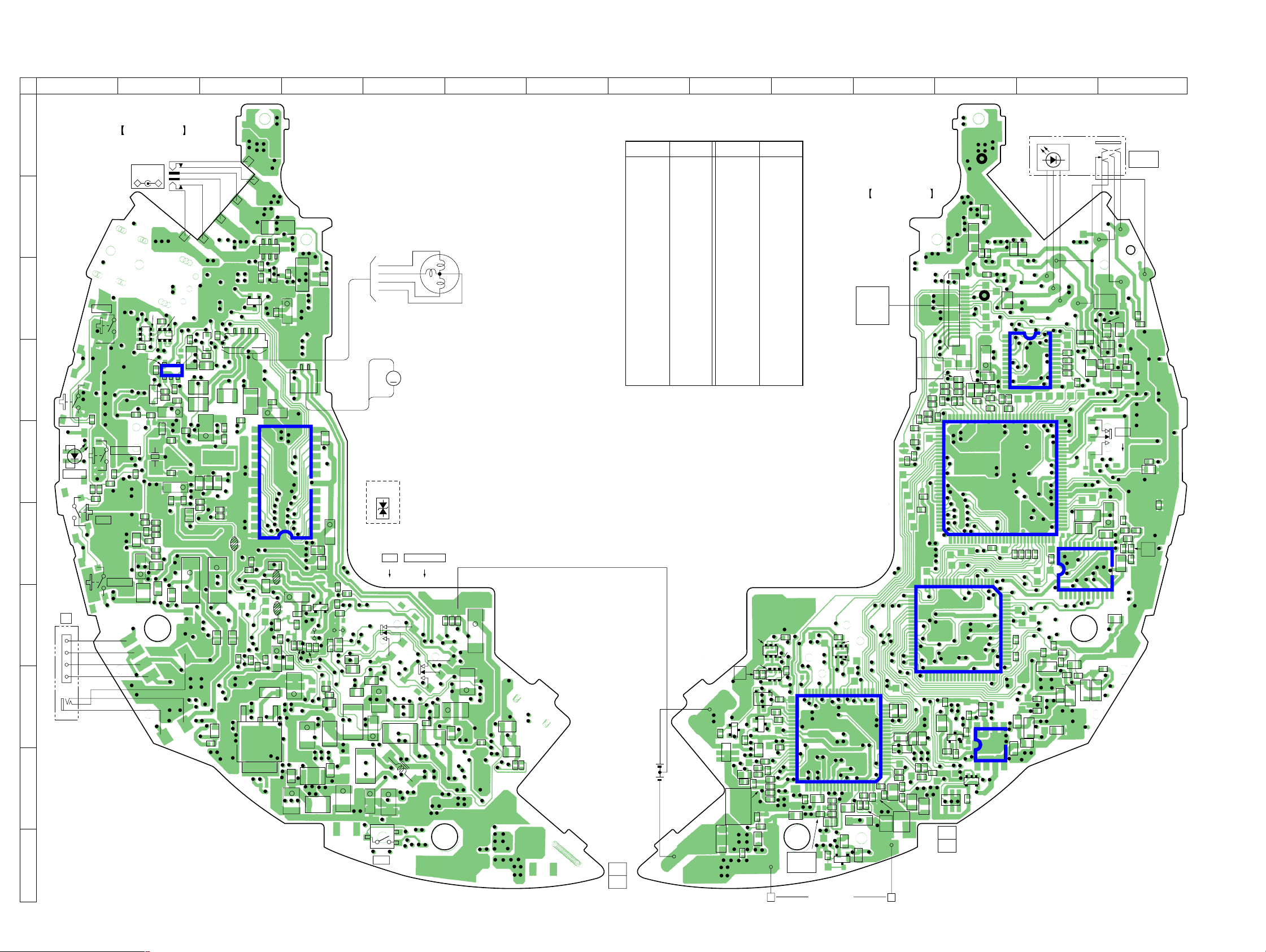
5-5. PRINTED WIRING BOARD
1 2 3 4 5 6 7 8 9 10 11 12 13 14
A
B
C
D
R819
S809
VOL –
D801
E
CHARGE
R818
F
J302
i
G
H
I
J
MAIN BOARD
(COMPONENT SIDE)
S808
VOL +
Q303
1E
1B
2C
R301
IC405
D407
R821
S805
x/CHARGE
R814
C814
R815
R816
R817
S807
.
C104
C106
C307
S806
> N
J401
EXT BATT
DC IN 4.5V
–
1C
2B
2E
C456
C812
D601
X601
R103
C107
C306
+
L303
+
2E
3
R471
AK
R470
C617
C625
R104
C105
R105
R108
R106
R206
C309
R302
2B
Q302
4
C618
C621
1C
+
R620
C619
C310
2C
1B
5
1
+
R625
1E
R467
C457
R621
FB601
+
C108
C450
L501
L502
D406
C451
+
FB602
C622
R634
K
A
C616
C620
FB302
C447
R468
L503
C615
R623
L602
R626
C623
SL808
+
C208
FB102
C801
C312
FB401
6
4
Q412
3
1
R477
B
C
E
R478
Q414
BCE
Q301
C608
14
4
L413
C501
C610
+
C607
1
CN501
IC602
26
R805
VDR801
R804
SL809
FB801
SL810
C805
D804
FB202
R458
+
C440
R801
C802
R802
D408
AK
EB
Q405
C
+
C804
C426
R479
C502
+
C807
+
C806
SL806
(OPEN)
C464
+
C425
FB402
12
CN502
13
1
L604
A
R808
C810
C811
C401
+
C444
L403
L405
K
D805
R813
R435
VDR403
R635
+
A
C462
C624
VDR601
D803
SL807
(TEST)
R474
L410
R439
C432
C808
R811
+
C809
FB803
R807
FB404
L401
R812
VDR804
L411
2
RED
1
BLK
D601,
D804, 805
S802
C446
+
+
C466
S804
OPEN
4
1
FB405
+
BLK
ORG
WHT
RED
S802
AVLS
LIMIT
NORM
C422
+
C433
M
L409
L408
M901
(SLED)
G
•
PROTECTION
S803
L404
S803
2
1
V
W
M902
(SPINDLE)
L406
C419
L402
R417
+
U
C412
C408
C424
R418
+
C413
+
R437
C411
R413
R416
R421
R444
1-682-611-
• Semiconductor Location
D303 H-13
D304 H-13
D305 H-13
D306 H-13
D307 H-13
D401 J-9
D403 B-12
D404 I-11
D405 I-11
D406 C-3
D407 D-2
D408 H-3
D601 E-2
D801 E-1
D803 G-4
D804 G-3
D805 G-4
IC301 F-13
IC402 I-12
IC403 H-10
IC404 D-13
R484
4
RECHARGEABLE
BATTERY
NC-6WM
2PSC. 2.4V
11
(11)
6
D401
Ref. No. LocationRef. No. Location
IC405 D-2
IC601 E-12
IC602 E-4
IC801 G-12
Q301 C-3
Q302 C-2
Q303 C-2
Q403 H-9
Q405 H-3
Q406 H-12
Q407 J-10
Q412 B-3
Q414 C-3
Q415 H-9
Q416 I-9
Q417 H-9
Q418 H-10
Q419 G-9
Q420 G-10
Q421 I-12
Q422 I-12
1E
2C
1B
Q419
Q418
1C
R490
R491
1E
B
E
Q403
C
Q417
BE
Q416
R420
C418
R436
AK
C405
3
1
R443
SDG
C
Q415
R483
R432
C417
C409
R442
R422
C421
R445
C423
R423
R426
– +CHARGE TEMINAL
2B
R419
C414
1B
R441
2E
2C
R440
41
C416
60
2E
R485
C429
R424
R457
R486
2B
J301
LINE OUT
TP418
(GND)
(OPTICAL)
MAIN BOARD
(CONDUCTOR SIDE)
OPTICAL
PICK-UP
BLOCK
DAX-25E
R602
C601
R601
R603
C603
R606
R614
C602
20
R609
C612
120
91
C611
R619
1
C613
R615
R607
R608
C614
C626
R622
21
IC801
R487
1E
2C
Q407
R447
R448
R425
BCE
Q420
2E
D404
VDR401
1B
2B
1C
21
80
AK
20
1
R449
R481
R463
D405
R454
C439
R450
C436
C465
C437
C438
R480
KA
40
R455
C442
C445
R460
R461
C434
41
C406
Q406
R465
R414
C443
C469
3
4
C431
Q421
1-682-611-
11
R409
B
C468
Q422
(11)
1C
40
IC403
61
R446
R459
C435
R429
R452
R456
D403
CN503
C
E
1
6
1
15
R604
2B
2C
KA
R410
TP601
(RF)
C604
C448
C606
C605
R605
R618
IC601
R482
8
R415
1
E
1B
1C
R488
C404
R305
R489
C449
+
12
R612
C609
R613
R632
1
60
R401
5
4
IC402
1
80
61
VDR304
C301
IC404
R610
R611
R631
C803
R806
D307
VDR202
R428
C403
VDR303
R630
R629
R307
R107
D303
KA
R628
R820
R207
R627
R310
6190
30
13
AK
24
24
1
60
31
C311
R309
VDR102
FB403
FB101
R469
C452
C453
C454
C455
C305
C304
IC301
R308
AK
D306
FB201
VDR201
VDR101
R101
C102
R102
C302
FB304
KA
KA
D304
D305
+
13
12
FB303
S801
HOLD
HOLD
C313
C202
OFF
C303
C204
VDR301
FB301
C207
R202
R201
R203
C205
R208
R204
R303
R803
R304
C206
VDR803
R492
R205
1414
 Loading...