

Sony DCR-PC101-101E Service Manual
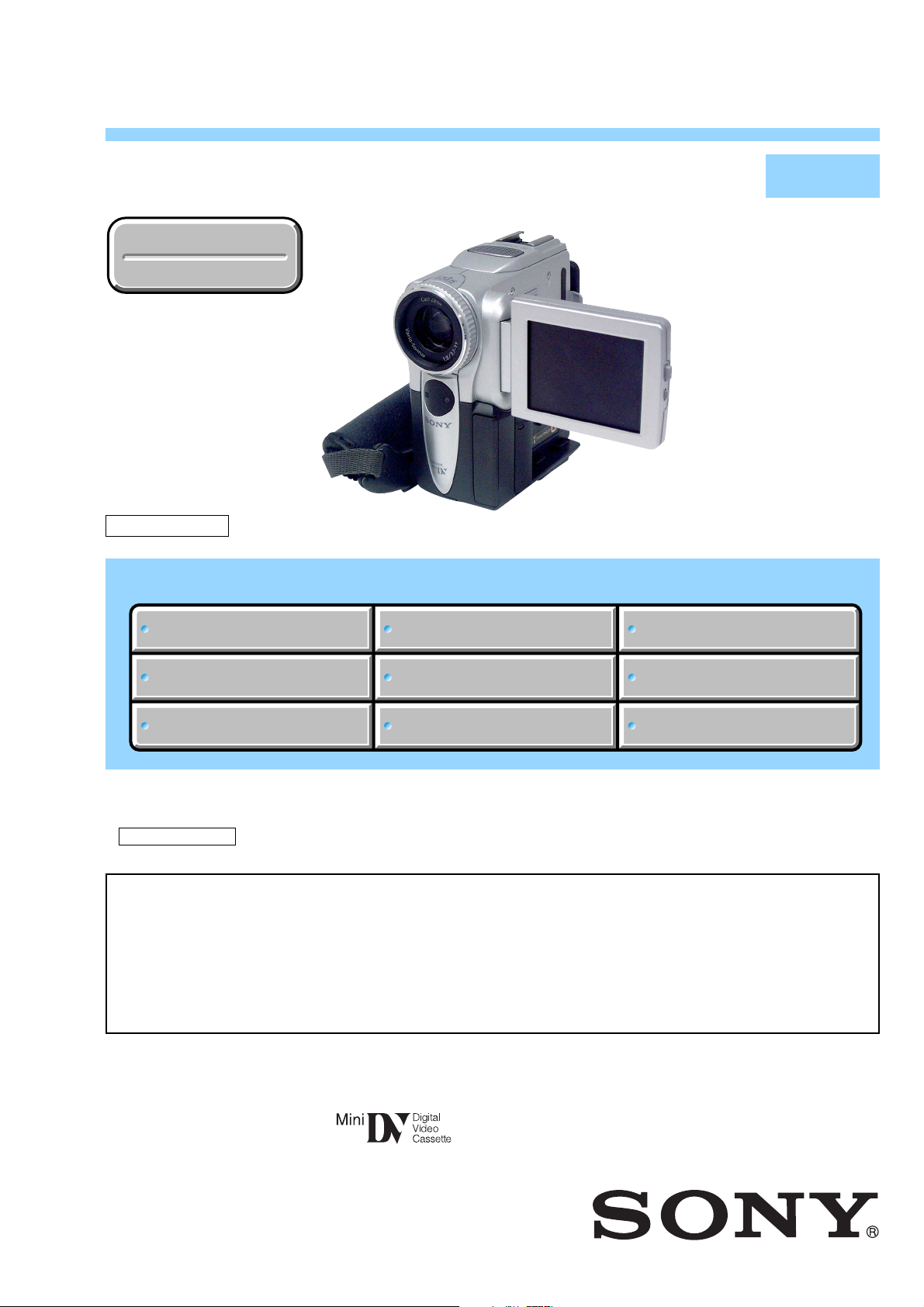
DCR-PC101/PC101E
RMT-814
SERVICE MANUAL
Ver 1.0 2002. 05
Revision History
Revision History
J MECHANISM
Link
Link
SPECIFICATIONS
SPECIFICATIONS
BLOCK DIAGRAMS
BLOCK DIAGRAMS
LEVEL 2
US Model
Canadian Model
East European Model
North European Model
Hong Kong Model
Australian Model
PRINTED WIRING BOARDS
PRINTED WIRING BOARDS
DCR-PC101
AEP Model
UK Model
Russian Model
DCR-PC101E
E Model
DCR-PC101/PC101E
Chinese Model
DCR-PC101E
Korea Model
DCR-PC101
Tourist Model
DCR-PC101/PC101E
SERVICE NOTE
SERVICE NOTE
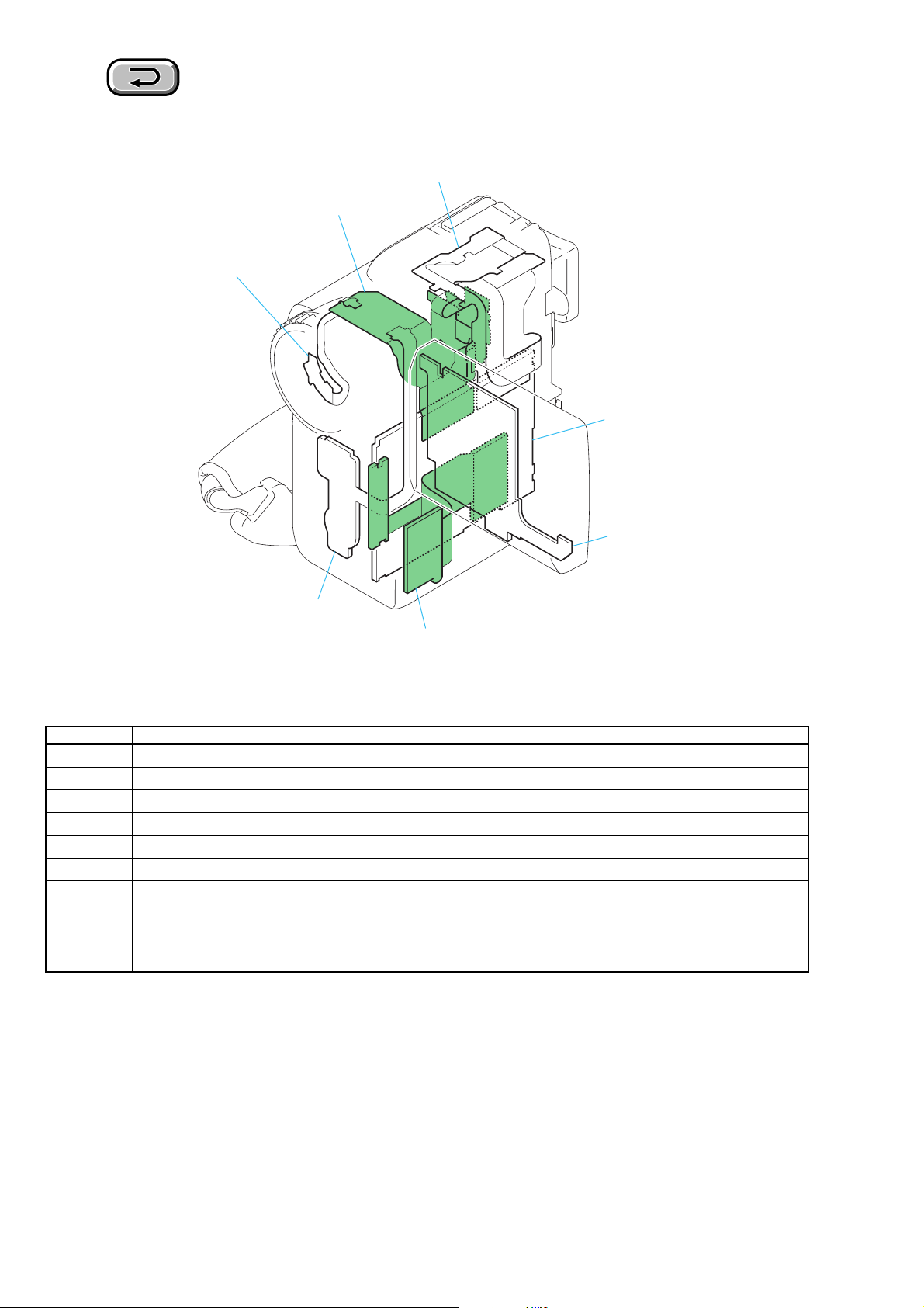
DISASSEMBLY
DISASSEMBLY
• For INSTRUCTION MANUAL, refer to SERVICE MANUAL, LEVEL 1 (992997141.pdf).
• For MECHANISM ADJUSTMENTS, refer to the “DV MECHANICAL ADJUSTMENT MANUAL VI
J MECHANISM ” (9-929-807-11).
• Reference No. search on printed wiring boards is available.
On the BJ-003, VC-284 boards
This service manual provides the information that is premised the circuit board replacement service and not intended repair
inside the BJ-003, VC-284 boards.
Therefore, schematic diagram, printed wiring board, waveforms, mounted parts location and electrical parts list of the BJ-003,
VC-284 boards are not shown.
The following pages are not shown.
Schematic diagram .............................Pages 4-9 to 4-50
Printed wiring board............................Pages 4-73 to 4-80
Waveforms ...........................................
FRAME SCHEMATIC DIAGRAMS
FRAME SCHEMATIC DIAGRAMS
SCHEMATIC DIAGRAMS
SCHEMATIC DIAGRAMS
Mounted parts location ..................
Electrical parts list.........................Pages 6-11, 6-16 to 6-25
Page 4-98 to 4-100
ADJUSTMENTS
ADJUSTMENTS
REPAIR PARTS LIST
REPAIR PARTS LIST
Page 4-103 to 4-105
DIGITAL VIDEO CAMERA RECORDER

DCR-PC101/PC101E
COVER
COVER
TM
SERIES
SPECIFICATIONS
Video camera
recorder
System
Video recording system
2
rotary heads
Helical scanning system
Audio recording system
2 rotary heads, PCM system
Quantization: 12 bits (Fs 32 kHz,
stereo 1, stereo 2), 16 bits
(Fs 48 kHz, stereo)
Video signal
DCR-PC101:
NTSC color, EIA standards
DCR-PC101E:
PAL color, CCIR standards
Usable cassette
Mini DV cassette with the
mark printed
Tape speed
SP: Approx. 18.81 mm/s
LP: Approx. 12.56 mm/s
Recording/playback time
(using cassette DVM60)
SP: 1 hour
LP: 1.5 hours
Fastforward/rewind time
(using cassette DVM60)
When using the battery pack:
Approx. 2 min. and 30 seconds
When using the AC power
adaptor:
Approx. 1 min. and 45 seconds
Viewfinder
Electric viewfinder (color)
Image device
3.8 mm (1/4.7 type) CCD
(Charge Coupled Device)
Gross: Approx. 1 070 000 pixels
Effective (still):
Approx. 1 000 000 pixels
Effective (moving):
Approx. 690 000 pixels
Lens
Carl Zeiss
Combined power zoom lens
Filter diameter 30 mm. (1 3/16 in.)
10× (Optical), 120× (Digital)
F = 1.8 - 2.0
Focal length
3.7 - 37 mm (5/32 - 1 1/2 in.)
When converted to a 35 mm still
camera
In CAMERA:
50 - 500 mm (2 - 19 3/4 in.)
In MEMORY:
42 - 420 mm (1 11/16 - 16 5/8 in.)
Color temperature
Auto, HOLD (Hold), nIndoor
(3 200K),
Outdoor (5 800K)
Minimum illumination
7 lx (lux) (F 1.8)
0 lx (lux) (in the NightShot mode)*
* Objects unable to be seen due to
the dark can be shot with
infrared lighting.
Input/Output connectors
S video input/output
4-pin mini DIN
Luminance signal: 1 Vp-p,
75 Ω (ohms), unbalanced, sync
negative
Chrominance signal:
DCR-PC101: 0.286 Vp-p
DCR-PC101E: 0.3 Vp-p
75 Ω (ohms), unbalanced
A/V (Audio/Video) input/output
AV MINI JACK, input/output
auto switch
Video signal: 1 Vp-p, 75 Ω (ohms),
unbalanced, sync negative
Audio signal: 327 mV, (at output
impedance more than 47 kΩ
(kilohms) )
Input impedance with more than
47 kΩ (kilohms)
Output impedance with less than
2.2 kΩ (kilohms)
DV input/output
4-pin connector
Headphone jack
Stereo minijack (ø 3.5 mm)
LANC jack
Stereo mini-minijack (ø 2.5 mm)
USB jack
mini-B
MIC jack
Minijack, 0.388 mV low impedance
with 2.5 to 3.0 V DC, output
impedance 6.8 kΩ (kilohms)
(ø 3.5 mm)
Stereo type
LCD screen
Picture
6.2 cm (2.5 type)
50.3 × 37.4 mm (2 × 1 1/2 in.)
Total dot number
211 200 (960 × 220)
General
Power requirements
7.2 V (battery pack)
8.4 V (AC power adaptor)
Average power consumption
(when using the battery pack)
During camera recording using
LCD:
DCR-PC101: 4.0 W
DCR-PC101E: 3.9 W
Viewfinder:
DCR-PC101: 3.3 W
DCR-PC101E: 3.2 W
Operating temperature
0 °C to 40 °C (32 °F to 104 °F)
Storage temperature
–20 °C to +60 °C (–4 °F to +140 °
Dimensions (approx.)
55 × 105 × 99 mm
(2 1/4 × 4 1/4 × 4 in.) (w/h/d)
Mass (approx.)
480 g (1 lb 0 oz)
excluding the battery pack and
cassette
580 g (1 lb 4 oz)
including the battery pack,
NP-FM50, cassette DVM60 and
lens cap
AC power adaptor
Power requirements
100 - 240 V AC, 50/60 Hz
Power consumption
23 W
Output voltage
DC OUT: 8.4 V, 1.5 A during
operation
Operating temperature
0 °C to 40 °C (32 °F to 104 °F)
Storage temperature
–20 °C to +60 °C (–4 °F to +140 °
Dimensions (approx.)
125 × 39 × 62 mm
(5 × 1 9/16 ×2 1/2 in.) (w/h/d)
excluding projecting parts
Mass (approx.)
280 g (9.8 oz)
excluding the power cord
Battery pack
Maximum output voltage
DC 8.4 V
Output voltage
DC 7.2 V
Capacity
8.5 Wh (1 180 mAh)
Dimensions (approx.)
38.2 × 20.5 × 55.6 mm
(1 9/16 × 13/16 × 2 1/4 in.)
(w/h/d)
Mass (approx.)
76 g (2.7 oz)
Type
Lithium ion
F)
“Memory Stick”
Memory
Flash memory
8MB: MSA-8A
Operating voltage
2.7-3.6V
Power consumption
Approx. 45mA during operation
Approx. 130µA in tape recording
standby
Dimensions (approx.)
50 × 2.8 × 21.5 mm
(2 × 1/8 × 7/8 in.) (w/h/d)
Mass (approx.)
4 g (0.14 oz)
Design and specifications are
subject to change without notice.
F)
— 2 —
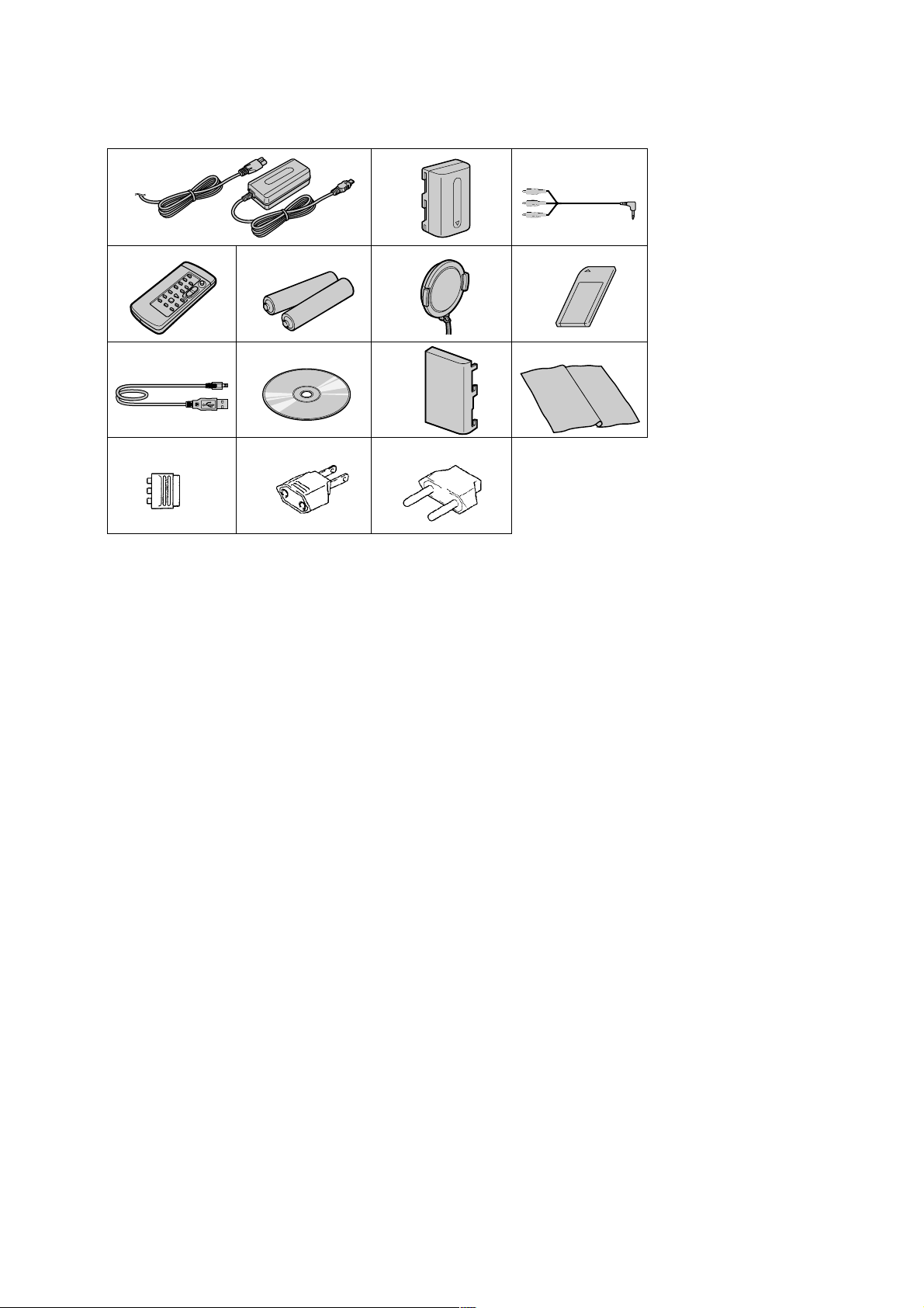
Supplied accessories
DCR-PC101/PC101E
4
8
qs qfqd
1 AC-L10A/L10B/L10C AC power
adaptor (1), Power cord (1)
2 NP-FM50 battery pack (1)
3 A/V connecting cable (1)
4 Wireless Remote Commander (1)
5 Size AA (R6) battery for Remote
Commander (2)
6 Lens cap (1)
7 “Memory Stick” (1)
8 USB cable (1)
5
9
21
6
q;
9 CD-ROM (SPVD-008 USB Driver)
q; Battery terminal cover (1)
qa Cleaning cloth (1)
qs 21-pin adaptor
DCR-PC101: AEP, UK, EE, NE, RU
qd 2-pin conversion adaptor (1)
DCR-PC101E: E, HK/PC101E: E, HK
qf 2-pin conversion adaptor (1)
DCR-PC101: JE/PC101E: JE
3
7
qa
(1)
(1)
— 3 —

DCR-PC101/PC101E
Danger of explosion if battery is incorrectly replaced.
CAUTION
Replace only with the same or eqivalent type.
SAFETY-RELATED COMPONENT WARNING!!
COMPONENTS IDENTIFIED BY MARK 0 OR DOTTED LINE WITH
MARK 0 ON THE SCHEMATIC DIAGRAMS AND IN THE PARTS
LIST ARE CRITICAL TO SAFE OPERATION. REPLACE THESE
COMPONENTS WITH SONY PARTS WHOSE PART NUMBERS
APPEAR AS SHOWN IN THIS MANUAL OR IN SUPPLEMENTS
PUBLISHED BY SONY.
SAFETY CHECK-OUT
After correcting the original service problem, perform the following
safety checks before releasing the set to the customer.
1. Check the area of your repair for unsoldered or poorly-soldered
connections. Check the entire board surface for solder splashes
and bridges.
2. Check the interboard wiring to ensure that no wires are
"pinched" or contact high-wattage resistors.
3. Look for unauthorized replacement parts, particularly
transistors, that were installed during a previous repair . Point
them out to the customer and recommend their replacement.
4. Look for parts which, through functioning, show obvious signs
of deterioration. Point them out to the customer and
recommend their replacement.
5. Check the B+ voltage to see it is at the values specified.
6. Flexible Circuit Board Repairing
• Keep the temperature of the soldering iron around 270˚C
during repairing.
• Do not touch the soldering iron on the same conductor of the
circuit board (within 3 times).
• Be careful not to apply force on the conductor when soldering
or unsoldering.
ATTENTION AU COMPOSANT AYANT RAPPORT
À LA SÉCURITÉ!
LES COMPOSANTS IDENTIFÉS P AR UNE MARQUE 0 SUR LES
DIAGRAMMES SCHÉMA TIQUES ET LA LISTE DES PIÈCES SONT
CRITIQUES POUR LA SÉCURITÉ DE FONCTIONNEMENT. NE
REMPLACER CES COMPOSANTS QUE PAR DES PIÈSES SONY
DONT LES NUMÉROS SONT DONNÉS DANS CE MANUEL OU
DANS LES SUPPÉMENTS PUBLIÉS PAR SONY.
Unleaded solder
Boards requiring use of unleaded solder are printed with the leadfree mark (LF) indicating the solder contains no lead.
(Caution: Some printed circuit boards may not come printed with
the lead free mark due to their particular size.)
: LEAD FREE MARK
Unleaded solder has the following characteristics.
• Unleaded solder melts at a temperature about 40°C higher than
ordinary solder.
Ordinary soldering irons can be used but the iron tip has to be
applied to the solder joint for a slightly longer time.
Soldering irons using a temperature regulator should be set to
about 350°C.
Caution: The printed pattern (copper foil) may peel away if the
heated tip is applied for too long, so be careful!
• Strong viscosity
Unleaded solder is more viscous (sticky, less prone to flow) than
ordinary solder so use caution not to let solder bridges occur such
as on IC pins, etc.
• Usable with ordinary solder
It is best to use only unleaded solder but unleaded solder may
also be added to ordinary solder.
— 4 —

DCR-PC101/PC101E
TABLE OF CONTENTS
Section Title Page Section Title Page
1. SERVICE NOTE
1-1. Service Note ····································································1-1
1. Power Supply During Repairs ·········································1-1
2. To Take Out a Cassette when Not Eject (Force Eject) ····1-1
1-2. Self-diagnosis Function ···················································1-2
1. Self-diagnosis Function ···················································1-2
2. Self-diagnosis Display·····················································1-2
3. Service Mode Display ·····················································1-2
4. Self-diagnosis Code Table ···············································1-3
2. DISASSEMBLY
2-1. LCD Cabinet (R) Assembly ············································2-2
LCD Block Service Position ···········································2-2
2-2. Cabinet (R) Block Assembly···········································2-3
2-3. Lens (-EVF) Block Section ·············································2-3
2-4. Lens Block·······································································2-4
2-5. CF-089 Board ··································································2-4
2-6. VC-284 Board ·································································2-5
2-7. Mechanism Deck ·····························································2-5
2-8. Cabinet (G) Assembly ·····················································2-6
2-9. Control Switch Block (FK-2850) ····································2-7
Note for Installation of Control Switch Block
(FK-2850) ········································································2-7
2-10. Control Switch Block (PS-2850) ·····································2-8
2-11. Cabinet (BT) Block ·························································2-8
2-12. BJ-003 Board ···································································2-9
2-13. LCD Section ····································································2-9
2-14. PD-116 Board ································································ 2-10
2-15. FP-470 Board ································································2-11
Position to Install FP-470 Board When Installing
LCD Hinge Assembly, Blind Plate Assembly ···············2-12
Installation of FP-470 Flexible Board,
Harness (PB-051) ··························································2-12
Note for Installation of LCD Hinge Block ····················2-12
Position of Connector Retainer Sheet ···························2-12
Service Position to Check the VTR Section··················2-13
Service Position to Check the CAMERA Section·········2-14
2-16. Flexible Boards Location ··············································2-15
2-17. Circuit Boards Location ················································2-16
3. BLOCK DIAGRAMS
3-1. Overall Block Diagram (1/4)···········································3-1
3-2. Overall Block Diagram (2/4)···········································3-3
3-3. Overall Block Diagram (3/4)···········································3-5
3-4. Overall Block Diagram (4/4)···········································3-7
3-5. Power Block Diagram (1/2)·············································3-9
3-6. Power Block Diagram (2/2)···········································3-11
4. PRINTED WIRING BOARDS AND
SCHEMATIC DIAGRAMS
4-1. Frame Schematic Diagrams
Frame Schematic Diagram (1/2) ·····································4-1
Frame Schematic Diagram (2/2) ·····································4-3
4-2. Schematic Diagrams························································4-5
CF-089(CCD IMAGER) ·················································4-7
PD-166 (1/2)
(LCD DRIVER, TIMING GENERATOR) ···················4-51
PD-166 (2/2) (BACK LIGHT) ······································4-53
ME-020 (1/2) (MIC AMP) ············································4-55
ME-020 (2/2) (EVF, EVF BACK LIGHT, JACK) ········4-57
FP-100, FP-102, FP-228 FLEXIBLE····························4-59
MF-326 (MANUAL FOCUS SENSOR)·······················4-61
NS-014 (REMOTE COMMANDER RECEIVER)·······4-62
CONTROL SWITCH BLOCK (FK-2850) ···················4-63
CONTROL SWITCH BLOCK (PS-2850)···················· 4-65
FP-470 FLEXIBLE ·······················································4-66
4-3. Printed Wiring Boards ···················································4-67
CF-089··········································································· 4-69
PD-166···········································································4-81
ME-020··········································································4-85
FP-100, FP-102, FP-228 FLEXIBLE···························· 4-89
MF-326 ··········································································4-91
NS-014···········································································4-93
4-4. Waveforms·····································································4-97
4-5. Mounted Parts Location ··············································4-102
5. ADJUSTMENTS
Before Starting Adjustment ·······················································5-1
1-1. Adjusting Items when Replacing
Main Parts and Boards ····················································5-2
5-1. Camera Section Adjustments··········································· 5-4
1-1. Preparations before Adjustment (CAMERA Section)·····5-4
1-1-1.List of Service Tools························································5-4
1-1-2.Preparations ·····································································5-5
1-1-3.Precaution ········································································5-7
1-2. Initialization of 8, A, B, C, D, E, F, 1B, 1E,
1F Page Data ···································································5-8
1-2-1.Initialization of A, D Page Data ······································5-9
1. Initializing A, D Page Data··············································5-9
2. Modification of A, D Page Data ······································5-9
3. A Page Table··································································5-10
4. D Page Table··································································5-10
1-2-2.Initialization of 8, C Page Data ·····································5-11
1. Initializing 8, C Page Data ············································5-11
2. Modification of 8, C Page Data. ····································5-11
3. 8 Page Table···································································5-12
4. C Page Table ··································································5-12
1-2-3.Initialization of E, F, 1E, 1F Page Data ························· 5-14
1. Initializing of E, F, 1E, 1F Page Data ····························5-14
2. Modification of E, F, 1E, 1F Page Data·························5-14
3. E Page Table ··································································5-15
4. F Page Table ·································································· 5-16
5. 1E Page Table ································································5-18
6. 1F Page Table ································································ 5-19
1-2-4.Initialization of B, 1B Page Data···································5-20
1. Initializing of B, 1B Page Data ·····································5-20
2. Modification of B, 1B Page Data ··································5-20
3. B Page Table ··································································5-20
4. 1B Page Table ································································5-20
1-3. Camera System Adjustments·········································5-21
1. 66MHz/54MHz Origin Oscillation Adjustment ············5-21
2. Hall Adjustment·····························································5-21
3. MR Adjustment ····························································· 5-22
4. Flange Back Adjustment
(Using the Minipattern Box) ·········································5-23
5. Flange Back Adjustment
(Using the Flange Back Adjustment Chart
and Subject More than 500 m Away) ····························5-24
6. Flange Back Check························································5-25
7. MAX GAIN Adjustment ··············································· 5-25
8. F No. & ND Light Quality Standard Data Input ···········5-26
9. Mechanical Shutter Adjustment ····································5-26
10. Picture Frame Setting ···················································· 5-27
11. Color Reproduction Adjustment····································5-28
12. AWB & LV Standard Data Input ···································5-29
13. Auto White Balance Adjustment ··································· 5-30
14. Auto White Balance Check ···········································5-31
— 5 —

DCR-PC101/PC101E
Section Title Page Section Title Page
15. Steady Shot Check·························································5-32
16. CCD Black Defect Adjustment ·····································5-32
17. CCD Defect Check························································5-33
1-4. Color Electronic Viewfinder System Adjustments ········5-34
1. VCO Adjustment (VC-284 Board)································5-34
2. Back Light Adjustment (VC-284 Board) ······················ 5-35
3. RGB AMP Adjustment (VC-284 Board)·······················5-35
4. Contrast Adjustment (VC-284 Board)···························5-36
5. White Balance Adjustment (VC-284 Board)·················5-36
1-5. LCD System Adjustments ·············································5-37
1. VCO Adjustment (PD-166 Board) ································5-37
2. RGB AMP Adjustment (PD-166 Board) ·······················5-38
3. Black Limit Adjustment (PD-166 Board) ·····················5-38
4. PSIG GRAY Adjustment (PD-166 Board) ····················5-39
5. Contrast Adjustment (PD-166 Board) ···························5-39
6. Center Voltage Adjustment (PD-166 Board) ·················5-40
7. V-COM Adjustment (PD-166 Board)····························5-40
8. White Balance Adjustment (PD-166 Board)················· 5-41
5-2. Mechanism Section Adjustments ··································5-42
2-1. How to Enter Record Mode Without Cassette ··············5-42
2-2. How to Enter Playback Mode Without Cassette ···········5-42
2-3. Tape Path Adjustment····················································5-42
5-3. Video Section Adjustments ···········································5-43
3-1. Preparations before Adjustments···································5-43
3-1-1.Equipment Required······················································ 5-43
3-1-2.Precautions on Adjusting···············································5-44
3-1-3.Adjusting Connectors ····················································5-45
3-1-4.Connecting the Equipment ············································5-45
3-1-5.Alignment T apes····························································5-46
3-1-6.Input/Output Level and Impedance ·······························5-46
3-2. System Control System Adjustments ····························5-47
1. Initialization of 8, A, B, C, D, E, F, 1B, 1E,
1F Page Data ·································································5-47
2. Touch Panel Adjustment················································5-47
3. Node Unique ID No. Input ············································5-48
3-1. Input of Company ID ····················································5-48
3-2. Input of Serial No. ·························································5-48
3-3. Servo and RF System Adjustments ······························5-50
1. CAP FG Duty Adjustment (VC-284 Board) ················· 5-50
2. PLL f0 & LPF f0 Pre-Adjustment (VC-284 Board) ·······5-50
3. Switching Position Adjustment (VC-284 Board)··········5-51
4. AGC Center Level and APC & AEQ Adjustment ·········5-51
4-1. Preparations before Adjustments···································5-51
4-2. AGC Center Level Adjustment (VC-284 Board) ··········5-52
4-3. APC & AEQ Adjustment (VC-284 Board) ··················5-52
5. PLL f0 & LPF f0 Final Adjustment (VC-284 Board)·····5-53
3-4. Video System Adjustments············································5-54
1. Chroma BPF f0 Adjustment (VC-284 Board)················5-54
2. S VIDEO OUT Y Level Adjustment
(VC-284 Board)·····························································5-55
3. S VIDEO OUT Chroma Level Adjustment
(VC-284 Board)·····························································5-55
4. VIDEO OUT Level Check (VC-284 Board)·················5-56
3-5. Audio System Adjustments ···········································5-57
1. Playback Level Check ···················································5-57
2. Overall Level Characteristics Check ·····························5-57
3. Overall Distortion Check···············································5-57
4. Overall Noise Level Check············································ 5-58
5. Overall Separation Check··············································5-58
5-4. Service Mode·································································5-59
4-1. Adjustment Remote Commander ··································5-59
1. Using the Adjustment Remote Commander··················5-59
2. Precautions Upon Using the Adjustment
Remote Commander······················································ 5-59
4-2. Data Process ··································································5-60
4-3. Service Mode·································································5-61
1. Setting the Test Mode ····················································5-61
2. Emergence Memory Address ········································5-61
2-1. C Page Emergence Memory Address ····························5-61
2-2. EMG Code (Emergency Code) ·····································5-62
2-3. MSW Code ····································································5-63
3. Bit Value Discrimination ···············································5-64
4. Jack Check (1) ·······························································5-64
5. Jack Check (2) ·······························································5-64
6. Switch Check·································································5-65
7. Record of Use Check (1) ···············································5-66
8. Record of Use Check (2) ···············································5-66
9. Record of Self-diagnosis Check ····································5-67
6. REPAIR PARTS LIST
6-1. Exploded Views·······························································6-1
6-1-1.Main Section····································································6-1
6-1-2.Lens Block Section··························································6-2
6-1-3.LCD EVF Block Section ·················································6-3
6-1-4.Cabinet (L) Block Assembly ···········································6-4
6-1-5.Cabinet (BT) Assembly··················································· 6-5
6-1-6.LCD Block Assembly······················································6-6
6-1-7.Overall Mechanism Deck Section (J100)························6-7
6-1-8.LS Chassis Block Assembly············································6-8
6-1-9.Mechanism Chassis Block Assembly······························6-9
6-2. Electrical Parts List ·······················································6-10
* The color reproduction frame is shown on page 179
— 6 —
DCR-PC101/PC101E
COVER
COVER
SECTION 1
SERVICE NOTE
1-1. SERVICE NOTE
1. POWER SUPPLY DURING REPAIRS
In this unit, about 10 seconds after power is supplied to the battery terminal using the regulated power supply (8.4V), the po wer is shut of f so
that the unit cannot operate.
These following two methods are available to prevent this. Take note of which to use during repairs.
Method 1.
Use the AC power adaptor (AC-L10, AC-VQ800 etc.).
Method 2.
Connect the servicing remote commander RM-95 (J-6082-053-B) to the LANC jack, and set the commander switch to the “ADJ” side.
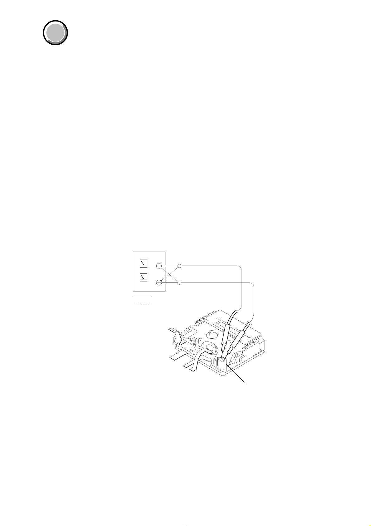
2. TO TAKE OUT A CASSETTE WHEN NOT EJECT (FORCE EJECT)
1 Refer to 2-2 to remove the cabinet (R) block assembly.
2 Refer to 2-3 to remove the lens (-EVF) block.
3 Refer to 2-6 to remove the VC-284 board.
4 Refer to 2-7 to remove the mechanism deck.
5 Supply +4.5V from the DC power supply to the loading motor and unload with a pressing the cassette compartment.
DC power supply
(+4.5Vdc)
: Unloading
: Loading
Loading motor
1-1
DCR-PC101/PC101E
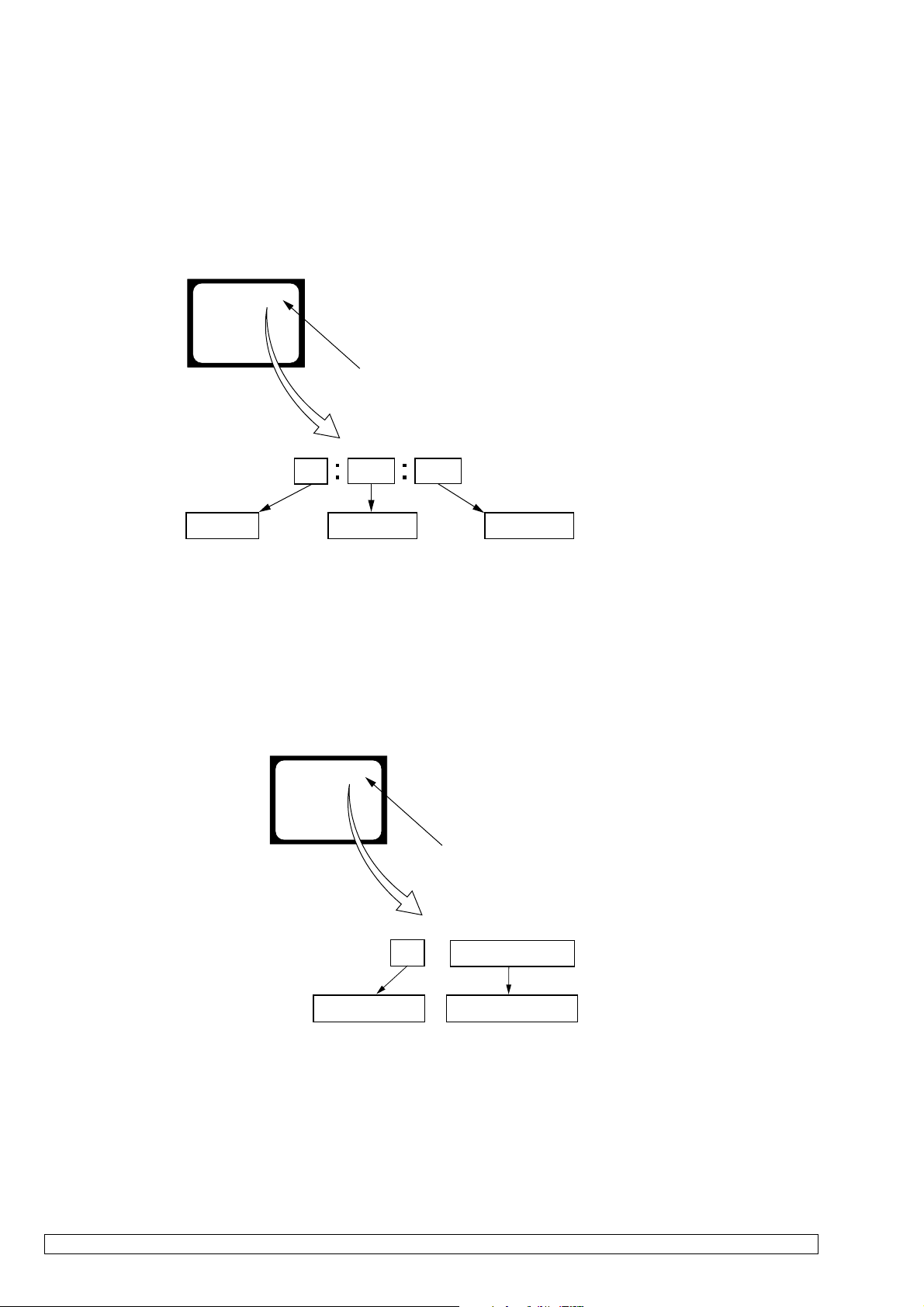
1-2. SELF-DIAGNOSIS FUNCTION
1. SELF-DIAGNOSIS FUNCTION
When problems occur while the unit is operating, the self-diagnosis
function starts working, and displays on the viewfinder or LCD
screen what to do. This function consists of two display; selfdiagnosis display and service mode display.
Details of the self-diagnosis functions are provided in the Instruction
manual.
Viewfinder or LCD screen
C : 3 1 : 1 1
Blinks at 3.2Hz
3 1C
Repaired by:
C : Corrected by customer
H : Corrected by dealer
E : Corrected by service
engineer
Indicates the appropriate
step to be taken.
E.g.
31 ....Reload the tape.
32 ....Tu r n o n power again.
Block
2. SELF-DIAGNOSIS DISPLAY
When problems occur while the unit is operating, the counter of the
viewfinder or LCD screen consists of an alphabet and 4-digit
numbers, which blinks at 3.2 Hz. This 5-character display indicates
the “repaired by:”, “block” in which the problem occurred, and
“detailed code” of the problem.
1 1
Detailed Code
Refer to “4. SELF-DIAGNOSIS CODE TABLE”.
3. SERVICE MODE DISPLAY
The service mode display shows the last self-diagnosis codes shown in the past.
3-1. Display Method
While pressing the “BA CK LIGHT” key , set the switch from OFF to “VCR or PLAYER”, and continue pressing the “BACK LIGHT” ke y for
5 seconds continuously. The service mode will be displayed, and the counter will show the backup No. and the 5-character self-diagnosis
codes.
Viewfinder or LCD screen
[3] C : 3 1 : 1 1
Lights up
[3]
Backup No.
Order of previous errors
C : 3 1 : 1 1
Self-diagnosis Codes
3-2. Backup No.
The backup No. in the [] indicates the order in which the problem occurred. (If the number of problems which occurred is less than 6, only the
number of problems which occurred will be shown.)
[1] : Occurred first time [4] : Occurred fourth time
[2] : Occurred second time [5] : Occurred fifth time
[3] : Occurred third time [6] : Occurred the last time
Note: Switching of the backup No. can’t be done.
3-3. End of Display
Turning OFF the power supply will end the service mode display.
Note: The “self-diagnosis display” data will not be erased (reset) when the lithium 3 V supply (NS-014 board BT001) is removed.
1-2
4. SELF-DIAGNOSIS CODE TABLE
Self-diagnosis Code
DCR-PC101/PC101E
Function
Repaired by:
C
C
C
C
C
C
C
C
C
C
C
C
C
C
C
C
C
C
C
C
C
C
C
E
E
E
E
E
Block
04
21
22
31
31
31
31
31
31
31
31
31
31
31
31
32
32
32
32
32
32
32
32
20
61
61
62
62
Detailed
Code
00
00
00
10
11
20
21
22
23
24
30
40
42
10
11
20
21
22
23
24
30
40
42
00
00
10
00
01
Symptom/State
Non-standard battery is used.
Condensation.
Video head is dirty.
LOAD direction. Loading does not
complete within specified time
UNLOAD direction. Loading does not
complete within specified time
T reel side tape slacking when unloading
Winding S reel fault when counting the
rest of tape.
T reel fault.
S reel fault.
T reel fault.
FG fault when starting capstan.
FG fault when starting drum.
FG fault during normal drum operations.
LOAD direction loading motor time-
out.
UNLOAD direction loading motor
time-out.
T reel side tape slacking when
unloading.
Winding S reel fault when counting the
rest of tape.
T reel fault.
S reel fault.
T reel fault.
FG fault when starting capstan.
FG fault when starting drum
FG fault during normal drum
operations
EEPROM data error
Difficult to adjust focus
(Cannot initialize focus.)
Zoom operations fault
(Cannot initialize zoom lens.)
Steadyshot function does not work well.
(With pitch angular velocity sensor output
stopped.)
Steadyshot function does not work well.
(With yaw angular velocity sensor output
stopped.)
Correction
Use the info LITHIUM battery.
Remove the cassette, and insert it again after one hour.
Clean with the optional cleaning cassette.
Load the tape again, and perform operations from the beginning.
Load the tape again, and perform operations from the beginning.
.
Load the tape again, and perform operations from the beginning.
Load the tape again, and perform operations from the beginning.
Load the tape again, and perform operations from the beginning.
Load the tape again, and perform operations from the beginning.
Load the tape again, and perform operations from the beginning.
Load the tape again, and perform operations from the beginning.
Load the tape again, and perform operations from the beginning.
Load the tape again, and perform operations from the beginning.
Remove the battery or power cable, connect, and perform
operations from the beginning.
Remove the battery or power cable, connect, and perform
operations from the beginning.
Remove the battery or power cable, connect, and perform
operations from the beginning.
Remove the battery or power cable, connect, and perform
operations from the beginning.
Remove the battery or power cable, connect, and perform
operations from the beginning.
Remove the battery or power cable, connect, and perform
operations from the beginning.
Remove the battery or power cable, connect, and perform
operations from the beginning.
Remove the battery or power cable, connect, and perform
operations from the beginning.
Remove the battery or power cable, connect, and perform
operations from the beginning.
Remove the battery or power cable, connect, and perform
operations from the beginning.
Initialize A, D page data (EEPROM data).
Inspect the lens block focus MR (Pin ql, w; of CF-089 board CN102)
when focusing is performed when the focus ring is rotated in the
focus manual mode, and the focus motor drive circuit (IC1301 of
VC-284 board) when the focusing is not performed.
Inspect the lens block zoom MR (
CN102
) when zooming is performed when the zoom lens is operated
and the zoom motor drive circuit (IC1301 of VC-284 board) when
zooming is not performed.
Inspect pitch angular velocity sensor (SE201 of CF-089 board)
peripheral circuits.
Inspect yaw angular velocity sensor (SE202 of CF-089 board)
peripheral circuits.
Pin 8, 0 of CF-089 board
1-3E
DCR-PC101/PC101E
COVER
COVER
SECTION 2
DISASSEMBLY
The following flow chart shows the disassembly procedure.
DCR-PC101/
PC101E
2-2. CABINET (R)
BLOCK ASSEMBLY
(Page 2-3)
2-3. LENS (-EVF) BLOCK
SECTION
(Page 2-3)
2-6. VC-284 BOARD
(Page 2-5)
2-1. LCD CABINET (R)
ASSEMBLY
(Page 2-2)
2-4. LENS BLOCK
(Page 2-4)
LCD BLOCK
SERVICE POSITION
(Page 2-2)
2-13. LCD SECTION
(Page 2-9)
2-11. CABINET (BT)
BLOCK
(Page 2-8)
2-14. PD-116 BOARD
(Page 2-10)
2-7. MECHANISM DECK
(Page 2-5)
2-8. CABINET (G)
ASSEMBLY
(Page 2-6)
2-9. CONTROL SWITCH
BLOCK (FK-2850)
(Page 2-7)
2-10. CONTROL SWITCH
BLOCK (PS-2850)
(Page 2-8)
SERVICE POSITION
TO CHECK
THE VTR SECTION
(Page 2-13)
2-5. CF-089 BOARD
(Page 2-4)
SERVICE POSITION
TO CHECK
THE CAMERA SECTION
(Page 2-14)
2-12. BJ-003 BOARD
(Page 2-9)
2-15. FP-470 BOARD
(Page 2-11)
2-1
DCR-PC101/PC101E
NOTE: Follow the disassembly procedure in the numerical order given.
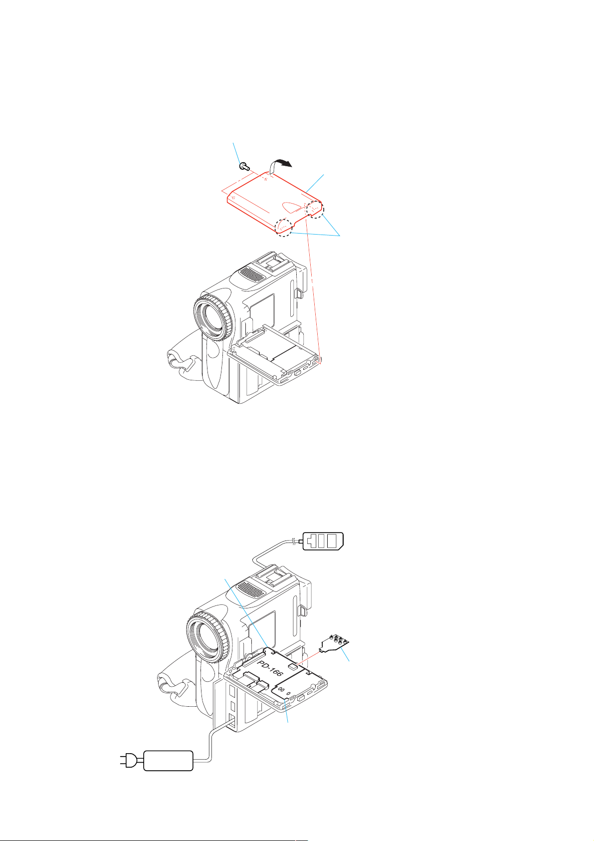
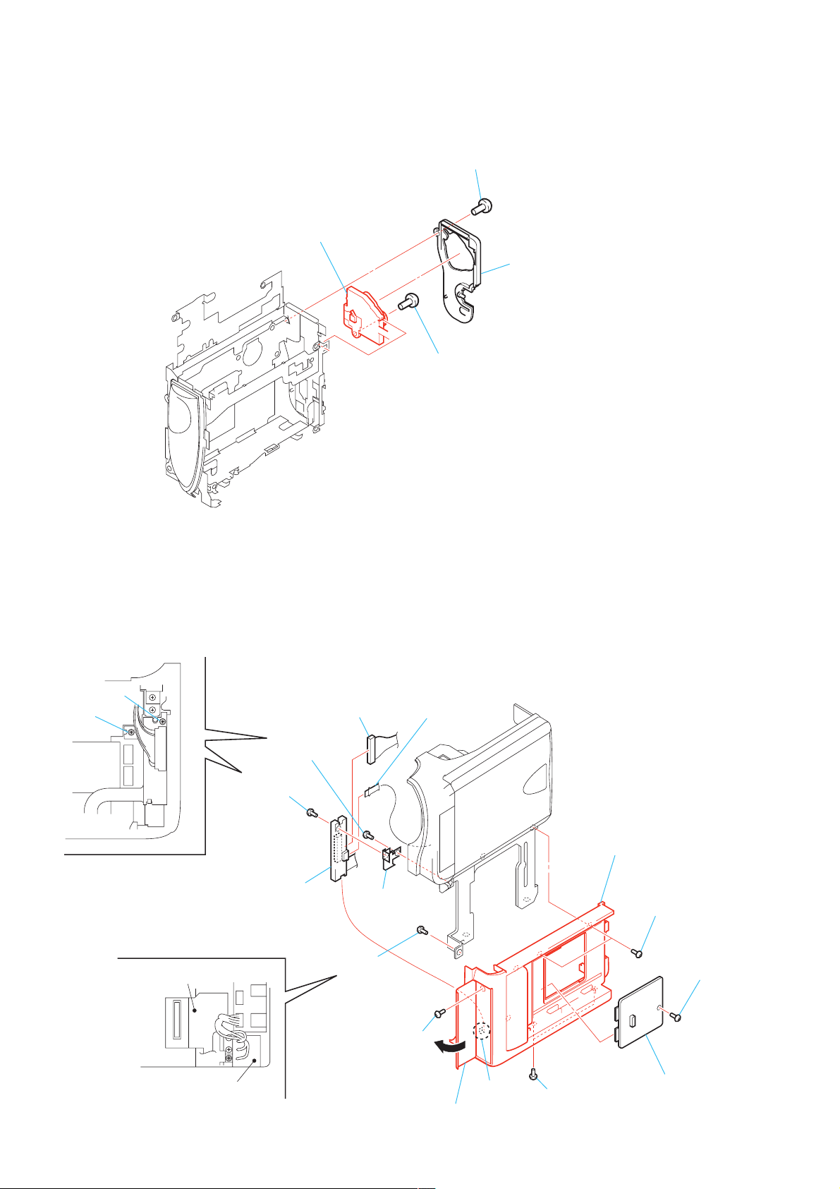
2-1. LCD CABINET (R) ASSEMBLY
1 Two screws
(M1.7)
3 LCD cabinet (R) assembly
2 Two claws
[LCD BLOCK SERVICE POSITION]
PD-166 board
AC IN
AC power
adaptor
Adjustment remote
commander (RM-95)
CPC jig for LCD panel
(J-6082-529-A)
Inverter transformer unit
2-2
DCR-PC101/PC101E
2-2. CABINET (R) BLOCK ASSEMBLY
2 Microphone cover
1 Screw (M1.7)
3 Two screws
(M1.7 × 4)
qs Compression
spring
qa Battery lock
When installing the battery lock,
two claws are met and attached in a slot of the
main frame assembly.
Main frame
assembly
Battery lock
Cabinet (rear)
Two claws
4 Two screw
(M1.7)
5 Two screw
(M1.7)
8 Remove the cabinet (R) block assembly
inthe direction of arrow.
7 Slide the eject knob
9 Connector
(BJ-003 board)
(CN1003)
0 Cabinet (R) block
assembly
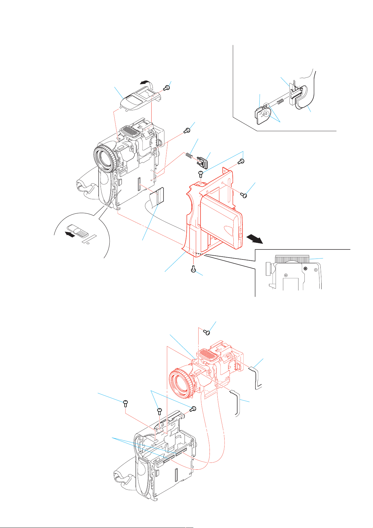
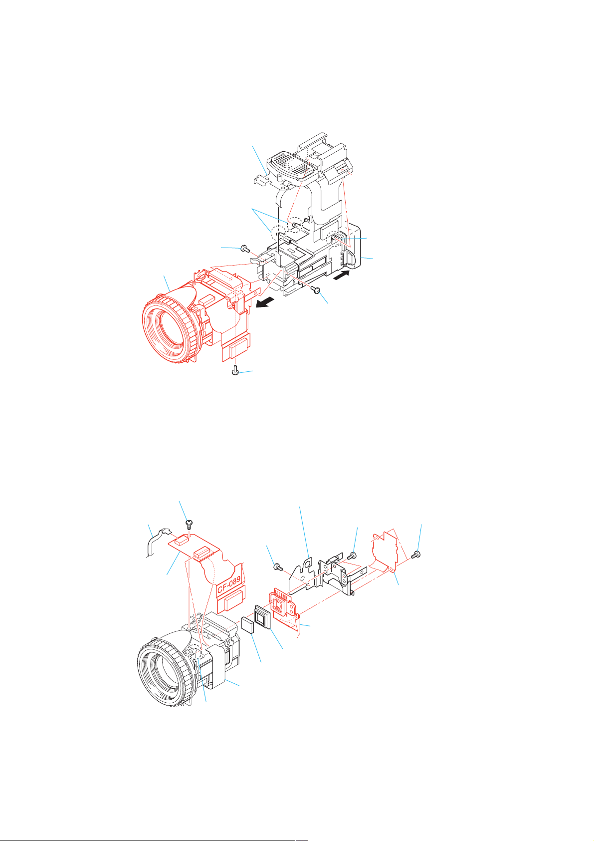
2-3. LENS (-EVF) BLOCK SECTION
7 Lens (-EVF) block
section
6 Screw
(M1.7 × 4)
4 Two screws
(M1.7)
Lens section
6 Screw
(M1.7)
— Bottom view —
5 Screw (M1.7)
2 Flexible board
(control switch block (PS-2850))
(CN402)
1 Flexible board (NS-014 board)
(CN104)
3 Two connectors
(CN1010, CN404)
2-3
DCR-PC101/PC101E
2-4. LENS BLOCK
3 Shoe frame
1 Two claws
9 Lens block
2-5. CF-089 BOARD
1 MF-326 board
(CN103)
6 Screw (M1.7)
2 Screw (M1.7)
8
5 Screw
(M1.7 × 4)
0 CD frame assembly
8 Screw
(M1.7 × 4)
2 Claw
4 Slide the VF lens assembly
A
7 Screw (M1.7)
9 Two screws
(M1.7 × 5)
in the dirrection of arrow A.
6 Two screws
(M1.7)
4 CF-089 board
(upper)
(CN102)
7 CF-089 board
(rear)
qa CF-089 board
(CCD block)
qs Seal rubber (W)
qd Optical filter block
5 Lens flexible board
(CN102)
3 Claw
2-4
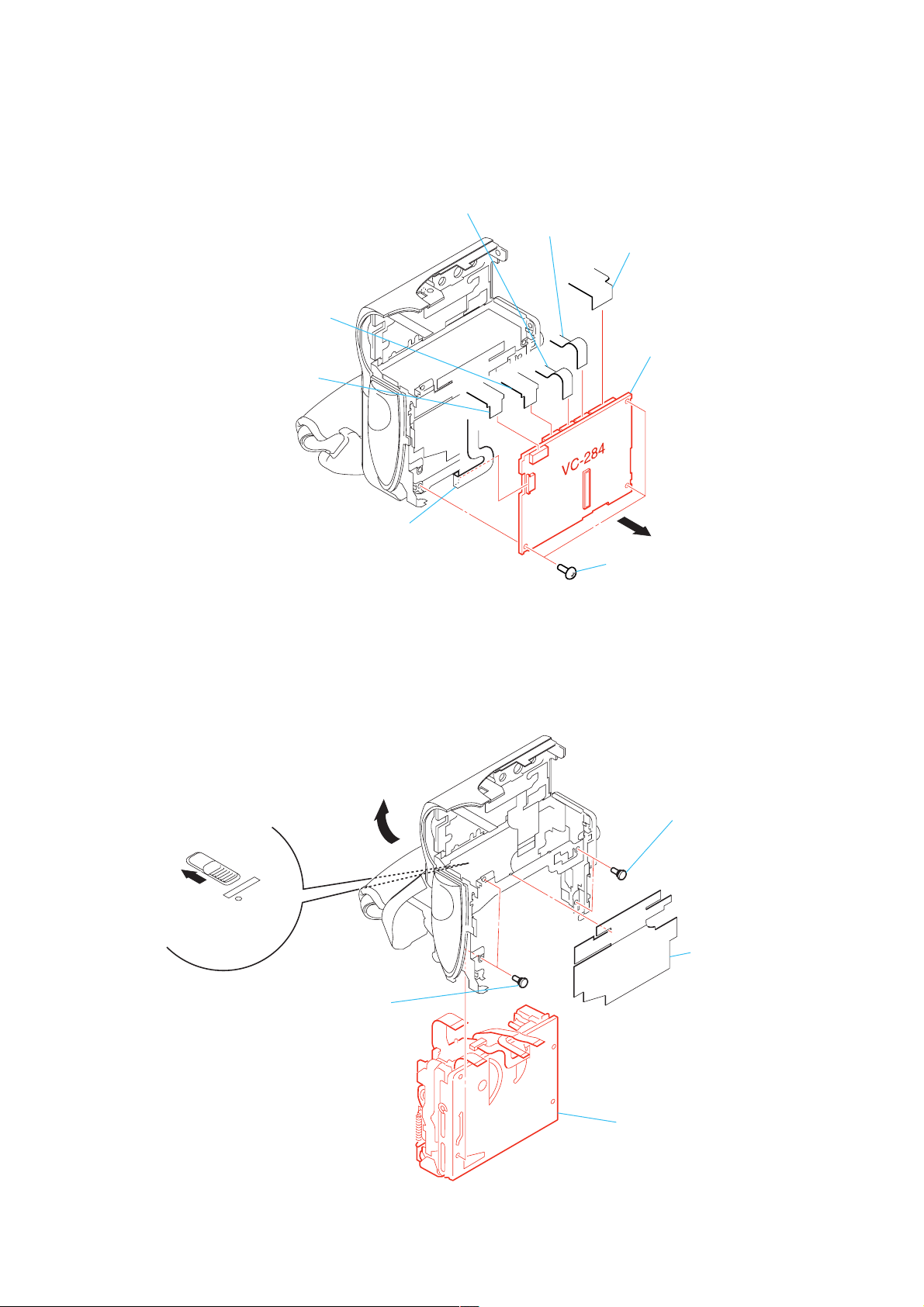
2-6. VC-284 BOARD
5 Flexible board
(CN1008)
6 Flexible board
(CN1007)
7 Flexible board
(CN1901)
DCR-PC101/PC101E
8 Flexible board
(CN1004)
2 Flexible board
(CN1009)
1 Flexible board
2-7. MECHANISM DECK
5 Open the
cabinet (G) assembly.
(CN1005)
9 VC-284 board
4 Remove the VC-284 board
in the direction of arrow.
3 Three screws
(M1.7)
2 Two screws
(M1.4 × 1.5)
4 Slide the eject knob.
1 Heat insulating sheet
3 Two screws
(M1.4 × 1.5)
6 Mechanism deck
2-5
DCR-PC101/PC101E
2-8. CABINET (G) ASSEMBLY
9 Open the jack cover
qd Cabinet (G) assembly
1 Special screw
(M2.6)
2 Sleeve
(front)
3 Hold grip assembly
0 Pull the bottom part of cabinet (G) assembly
in the direction of arrow, and then remove the claw.
4 Sleeve
(rear)
Charge lever
6 Screw
(M1.7)
5 Two screws
(M1.7)
7 Four screws
(M1.7 × 4)
qa
8 Two screws
(M1.7 × 4)
qs Eject knob
Eject knob
When install the eject knob,
charge lever is made into the position of a figure.
Note: Make sure to perform checking of operations
after the installation.
2-6
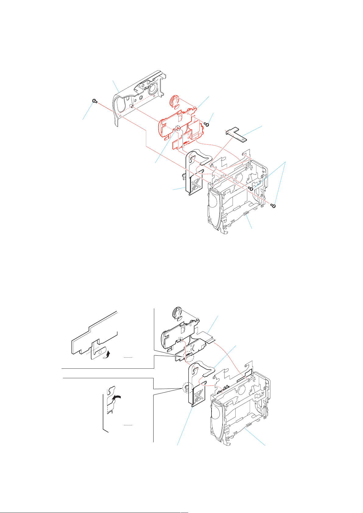
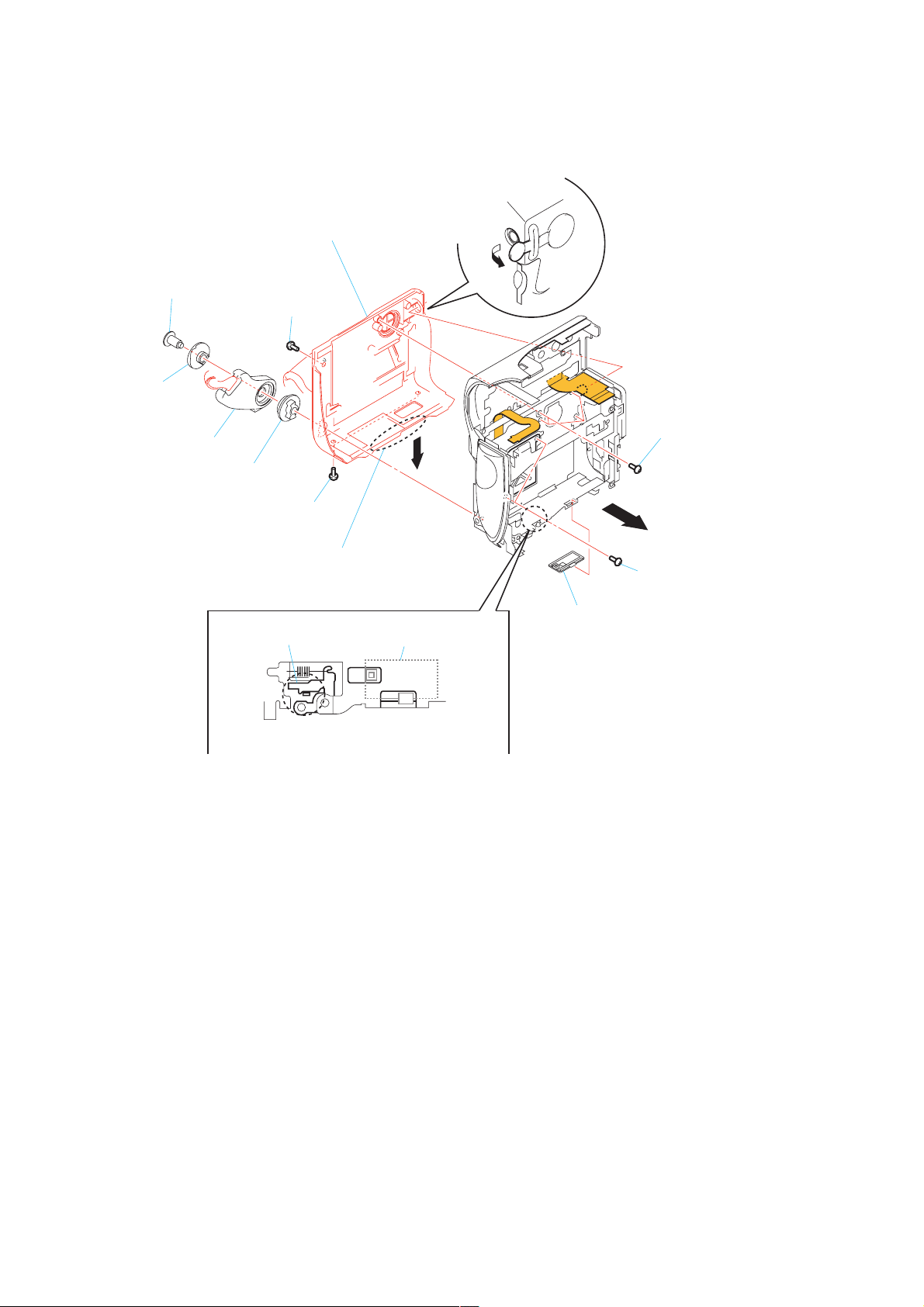
2-9. CONTROL SWITCH BLOCK (FK-2850)
6 Cabinet (L)
DCR-PC101/PC101E
9 Control switch block
(FK-2850)
5 Screw (M1.7 × 4)
1 Two screws
(M1.7)
7 Boss
8 Memory stick
connector
4 Reinforcement
2 Three screws
(M1.7 × 4)
3 Chassis section
[NOTE FOR INSTALLATION OF CONTROL SWITCH BLOCK (FK-2850)]
: Fold
: Fold
Memory stick connector
block
Pass the cable of the flexible of control switch block
through chassis block.
Pass FP-347 flexible board
through chassis block.
Chassis block
2-7
DCR-PC101/PC101E
2-10. CONTROL SWITCH BLOCK (PS-2850)
4 Control switch block
(PS-2850)
1 Screw (M1.7)
2 Cabinet (rear)
3 Screw (M1.7)
2-11. CABINET (BT) BLOCK
5
qs
5 Screw
(M1.7)
7 Remove the
BJ-003 board
BJ-003 board
qs Screw
(M1.7)
9 Connector
(CN007)
qd DV
qf Screw
(M1.7)
8 FP-470 flexible board
(CN007)
fixed plate
qg Cabinet (BT) block
3 Two screws
(M1.7)
1 Screw
(M1.7)
DC-IN connector
qa Screw
(M1.7)
0 Open the DC-IN lid
2-8
6 Claw
4 Two screws
2 CPC lid
(M1.7 × 4)
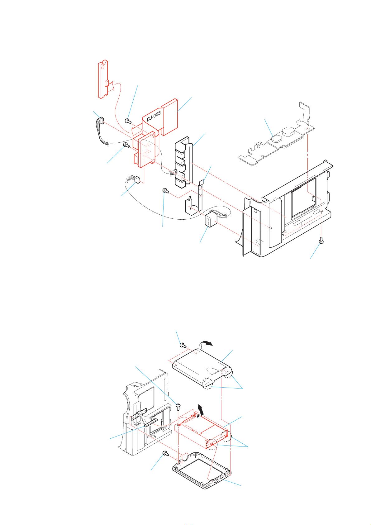
2-12. BJ-003 BOARD
DCR-PC101/PC101E
5 Screw (M1.7 × 4)
3 Connector
(battery terminal
board) (CN001)
7 BJ-003 board
2 Bottom flame section
8 Battery terminal
board
0 BJ frame
6 Screw (M1.7)
4 Connector
(battery terminal
board) (CN002)
9 Screw (M1.7 × 4)
qa Battery terminal
board
1 Two screws
(M1.7)
2-13. LCD SECTION
4 Two screws
7 Connector
(CN801)
1 Two screws
(M1.7)
3 LCD cabinet (R) assembly
(M1.7)
2 Two claws
9 LCD section
6 Two claws
5 Two screws
(M1.7)
8 LCD cabinet (L) assembly
2-9
DCR-PC101/PC101E
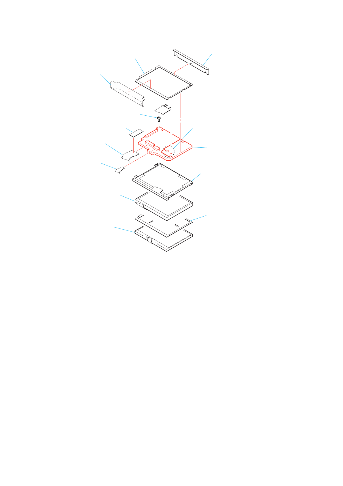
2-14. PD-166 BOARD
3 Panel protection sheet
1 Sheet (R)
2 Sheet (T)
qa Screw (M1.7)
8 Flexible board
(LCD) (CN804)
5 Flexible board
(panel (TP-1770))
(CN802)
6 Panel (TP-1770)
4 Tape
9 LCD unit
0 Remove three solders
qd PD-166 board,
inverter transformer block
qs Back light unit
7 Panel spacer
2-10
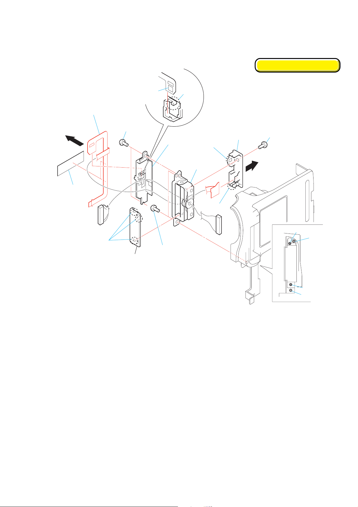
2-15. FP-470 FLEXIBLE BOARD
DCR-PC101/PC101E
NOTE FOR INSTALLATION
NOTE FOR INSTALLATION
qg FP-470 flexible board
4
1 Two connector
retainer sheet
7 Three claws
S4701
(Panel open)
3 Two screws
(M1.7)
8 Hinge cover
(upper)
5 Claw
6 Blind plate
assembly
qs LCD
2 Two screws
(M1.7 × 4)
0 Claw
hinge assembly
qd Claw
qf Hinge cover
(lower)
9 Screw (M1.7)
qa
3
2
2
3
2-11
DCR-PC101/PC101E
[POSITION TO INSTALL FP-470 BOARD
WHEN INSTALLING LCD HINGE
ASSEMBLY, BLIND PLATE ASSEMBLY]
Harness (PB-051)
Blind plate assembly
LCD hinge assembly
FP-470 flexible board
[NOTE FOR INSTALLATION OF LCD
HINGE BLOCK]
Hook this portion
on the cabinet (R)
to install the blind plate
assembly.
Blind plate assembly
LCD hinge block
FP-470 flexible board
Cabinet (R)
[INSTALLATION OF FP-470 FLEXIBLE
BOARD, HARNESS (PB-051)]
Harness (PB-051)
FP-470 flexible board
[POSITION OF CONNECTOR RETAINER
SHEET]
Hinge block assembly
FP-470
flexible board
Harness (PB-051)
Connector retainer
sheet
BJ-003 board
2-12
DCR-PC101/PC101E
ME-020 board
Adjustment remote
commander (RM-95)
AC power
adaptor
AC IN
Control switch block
(PS-2850) (10P)
Control switch block
(FK-2850)
DC-IN connector
BJ-003 board
VC-284 board
Mechanism deck
CPC-6 flexible jig
(J-6082-370-B)
CPC-6 terminal board jig
(J-6082-371-A)
When exiting the Forced VTR Power ON mode, connect the control
switch block (PS-2850) to the CN402 of ME-020 board. Or,
when ejecting the cassette, connect the control switch block (PS-1770)
to the CN402 of ME-020 board. and press the EJECT switch.
[SERVICE POSITION TO CHECK THE VTR SECTION]
Connection to Check the VTR Section
T o check the VTR section, set the VTR to the “Forced VTR po wer ON” mode. (Or , connect the control switch block (PS-2850) to the CN402
of ME-020 board and set the power switch to the “VIDEO” position.)
Operate the VTR function using the adjustment remote commander (with the HOLD switch set in the OFF position).
Setting the “Forced VTR Power ON” mode
1) Select page: 0, address: 01, and set data: 01.
2) Select page: D, address: 10, set data: 02 and press the P AUSE
button of the adjustment remote commander.
Exiting the “Forced VTR Power ON” mode
1) Select page: 0, address: 01, and set data: 01.
2) Select page: D, address: 10, data: 00, and press the PAUSE
button of the adjustment remote commander.
3) Select page: 0, address: 01, and set data: 00.
2-13
DCR-PC101/PC101E
[SERVICE POSITION TO CHECK THE CAMERA SECTION]
Connection to Check the Camera Section
T o check the camera section, set the camera to the “Forced camera po wer ON” mode. (Or, connect the control switch block (PS-2850) to the
CN-402 of ME-020 board and set the power switch to the “CAMERA” position.)
Operate the camera functions of the zoom and focus using the adjustment remote commander (with the HOLD switch set in the OFF
position).
Setting the “Forced Camera Power ON” mode
1) Select page: O, address: 01, and set data: 01.
2) Select page: D, address: 10, set data: 01 and press the PAUSE
button of the adjustment remote commander.
CPC-6 terminal board jig
(J-6082-371-A)
Control switch block
(FK-2850)
Seal rubber
Lens block
Optical filter
block
Two screws
(M1.7 × 5)
CPC-6 flexible jig
(J-6082-370-B)
Exiting the “Forced Camera Power ON” mode
1) Select page: O, address: 01, and set data: 01.
2) Select page: D, address: 10, data: 00, and press the PAUSE
button of the adjustment remote commander.
3) Select page : 0, address: 01, and set data: 00.
When exiting the
Forced Camera Power ON mode,
connect the control switch block (PS-2850)
to the CN402 of ME-020 board.
Adjustment remote
commander (RM-95)
ME-020 board
VC-284 board
Control switch block
(PS-2850) (10P)
BJ-003 board
DC-IN connector
CF-089 board
Mechanism deck
AC IN
2-14
AC power
adaptor
2-16. FLEXIBLE BOARDS LOCATION
DCR-PC101/PC101E
FP-347
Control switch block
(FK-2850)
Control switch block
(PS-2850)
FP-470
2-15
DCR-PC101/PC101E
2-17. CIRCUIT BOARDS LOCATION
CF-089
MF-326
ME-020
VC-284
PD-166
NS-014
BJ-003
Board Name Function
BJ-003 DC IN, DV/USB CONNECTOR
CF-089 CCD IMAGER
ME-020 MIC AMP, EVF, EVF BACK LIGHT, JACK
MF-326 MANUAL FOCUS SENSOR
NS-014 REMOTE COMMANDER RECEIVER
PD-166 LCD DRIVE, BACK LIGHT
VC-284 CAMERA PROCESSOR, LENS DRIVE, MPEG MOVIE/DIGITAL STILL PROCESS,
DV INTERFACE, REC/PB AMP, USB INTERFACE, VIDEO IN/OUT, EVF DRIVE,
MECHA DECK DRIVE, CAMERA/MECHA CONTROL,
HI CONTROL AUDIO IN/OUT, DC/DC CONVERTER
2-16E

COVER
COVER
Link
Link
DCR-PC101/PC101E
3. BLOCK DIAGRAMS
OVERALL BLOCK DIAGRAM (1/4)
OVERALL BLOCK DIAGRAM (1/4)
OVERALL BLOCK DIAGRAM (2/4) POWER BLOCK DIAGRAM (1/2)
OVERALL BLOCK DIAGRAM (2/4) POWER BLOCK DIAGRAM (1/2)
OVERALL BLOCK DIAGRAM (3/4) POWER BLOCK DIAGRAM (1/2)
OVERALL BLOCK DIAGRAM (3/4) POWER BLOCK DIAGRAM (1/2)
OVERALL BLOCK DIAGRAM (4/4)
OVERALL BLOCK DIAGRAM (4/4)
DCR-PC101/PC101E
COVER
COVER
SECTION 3
BLOCK DIAGRAMS
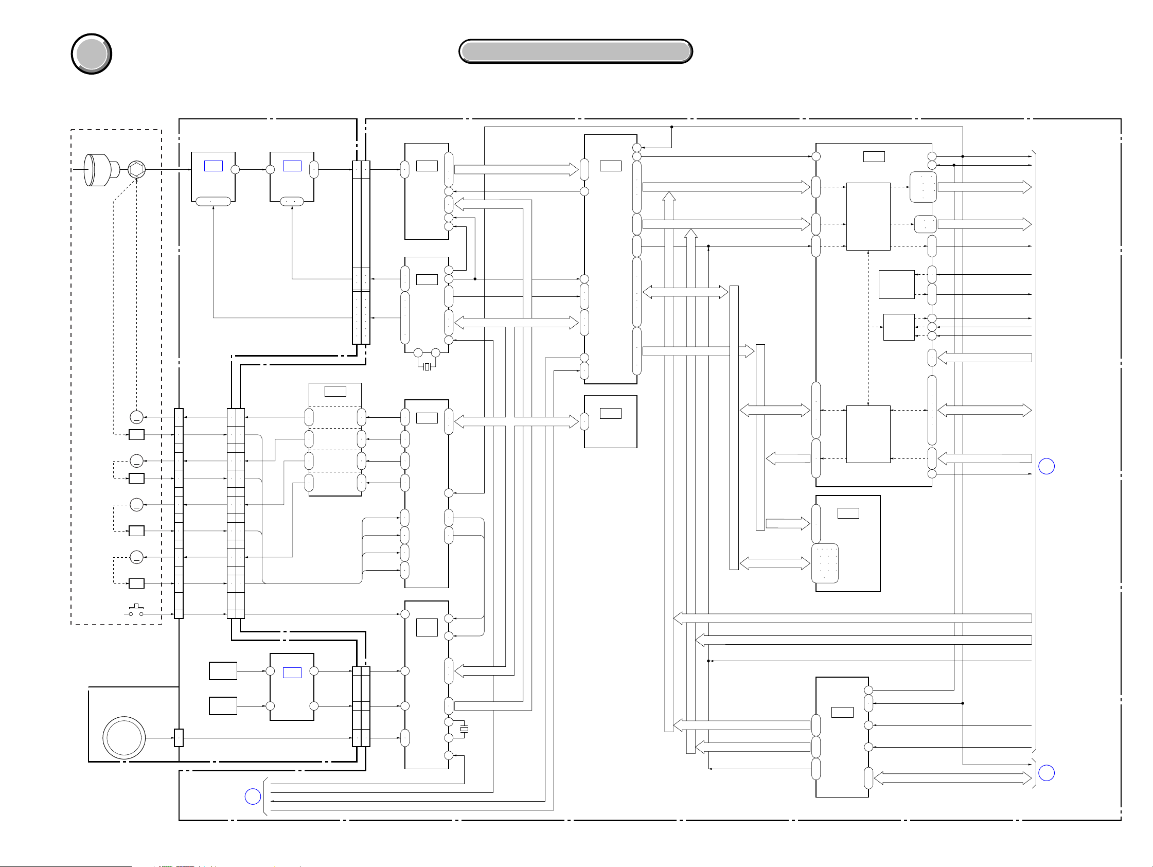
3-1. OVERALL BLOCK DIAGRAM (1/4)
LENS BLOCK
LENS
IRIS
METER
ND FILTER
METER
FOCUS
MOTOR
ZOOM
MOTOR
IRIS
(SHUTTER)
M
H
M
H
M
MR
M
MR
CF-089 BOARD (1/2)
IC301
CCD
IMAGER
1 - 4 10 - 12 1 13 14
CN102
IRIS DRIVE±
3
4
IRIS HALL±
2
6
ND DRIVE±
13
14
ND HALL±
12
16
FOCUS±
26
27
F MR A, B
19
20
ZOOM±
24
25
Z MR A, B
8
10
CCD OUT CCD OUT±
8
CN101
(2/4)
171817
232423
293029
353635
454645
373837
414241
252625
18
24
30
36
46
38
42
26
CN1010
(2/4)
IC305
11
S/H
3. BLOCK DIAGRAMS
3. BLOCK DIAGRAMS
( ) : Number in parenthesis ( ) indicates the division number of schematic diagram where the component is located.
VC-284 BOARD (1/4)
CN101
4
5
SHP, SHD, CLPDM
V1 - V4, RG, H1, H2
IC1301
(3/20)
5
IRIS
19
DRIVE
ND FILTER
7
DRIVE
17
2
FOCUS MOTOR
23
DRIVE
ZOOM MOTOR
4
DRIVE
21
(1/4)
83
85
71
73
84
65
67
68
70
77
79
80
13
14
15
16
9
10
11
12
CN1010
(1/4)
83
85
71
73
84
65
67
68
70
77
79
80
IRIS PWM,
IRIS EN
ND PWM,
ND EN
FC PWM,
FC EN
ZM PWM,
ZM EN
IRIS HALL±
ND HALL±
F MR A, B
Z MR A, B
30
31
A/D CONV.
16
17
22
9
GENERATOR
12
13
40
ı
42
44
30 29
10
11
8
9
ND FILTER
14
CONTROL
15
12
13
44
45
36
37
60
61
52
53
1
ı
IC1502
12
47
AGC,
48
20 65
(1/20)
44
45
16
19
PBLK
21
25
IC1501
33
TIMING
ı
35
(1/20)
1
2
47
6
X1502
66MHz : PC101
54MHz : PC101E
2
IC1304
5
6
FOCUS/
ZOOM/
IRIS/
(3/20)
SPCK
18
HALL AD
26
41
ND HALL
27
40
AD0 - AD13
TG HD,
TG VD,
TG FLD
CAM DD ON
CAM SI, CAM SO, CAM SCKCAM SI, CAM SO, CAM SCK
CLPOB
SH SO, SH SCKSH SO, SH SCK
CHCK
EXT STROBO
XSYS RST
44
ı
57
95
60
61
64
13
15
16
76
163
164
6
7
IC1601
CAMERA
PROCESSOR
(2/20)
IC1801
EVR
(1/20)
SPCK
97
96 177
1
3
169
170
173
175
4
7
8
10
133
137
140
142
145
146
149
154
102
109
114
118
121
ı
ı
ı
ı
ı
ı
ı
ı
ı
IYF Y0 - Y7
IYF C0 - C3
VCK
MDQ0 - MDQ15
MA0 - MA13
IYF Y0 - Y7
IYF C0 - C7
IFI HD, IFI VD, IFI OE
DATA BUS
IYF Y0 - Y7
IYF C0 - C7
IFI HD, IFI VD, IFI OE
MDQ0 - MDQ15
MA0 - MA13
ADDRESS BUS
MA0 - MA13
MDQ0 - MDQ15
76
ı
83
65
ı
72
84
ı
86
153
ı
156
158
ı
160
162
ı
170
128
ı
133
137
ı
144
20
ı
26
29
ı
35
2 4 5 7 8
10 11 13
42 44 45
47 48 50
51 53
MPEG MOVIE
PROCESS
DIGITAL STILL
PROCESS
IC1701
64M bit SDRAM
(4/20)
IC1704
(4/20)
CHARACTER
GENERATOR
AUDIO
99 101
103 106
108 111
113 115
91 93
95 97
74
44
117
ı
119
87
88
120
ı
123
61
62
59
47
48
11
ı
14
16
18
20
22
27
ı
34
2
ı
9
25
VFI HD, VFI VD, VFI OE
VSP SO, XVSP SCK
SPCK
AFCK
VFI Y0 - Y7
VFI C0 - C3
OSD HD, OSD VD
COL 0 - 3
ADAI2
ADAO2
SFD BCK
D0 LK - D15 LK
A16 LK - A23 LK
DSCK
OVERALL (2/4)
2
(PAGE 3-3)
NIGHT SHOT
FILTER DET.
MF-326 BOARD
PH730, 731
MANUAL
FOCUS
SENSOR
CN103
3
4
05
NT SHOT
SE202
YAW
SENSOR
SE201
PITCH
SENSOR
50 5017
OVERALL (4/4)
(PAGE 3-8)
12 18
8 2
MF A, B
ZOOM VR AD
CAM DD ON
EXT STROBO
1
XSYS RST
IC201
YAW/PITCH
SENSOR
AMP
CN101
YS OUT
PS OUT
(3/4)
XNS SW
4 4
3 3
535553
55
CN1010
(3/4)
41
130
129
210
211
IC2501
(1/2)
CAMERA
CONTROL
(15/20)
128
136
135
75
77
78
44
45
1
3
HALL AD
ND HALL
X2501
20MHz
IYF Y0 - Y7
IYF C0 - C3
IFI HD, IFI VD, IFI OE IFI HD, IFI VD, IFI OE
34
31
68
2
34
36
ı
38
IYF Y0 - Y7
IYF C0 - C7
IFI HD, IFI VD, IFI OE
52
59
42
49
36
38
ı
ı
ı
IC2001
VIDEO
A/D CONV.
(11/20)
3-1 3-2
AFCK
SPCK
IYF Y0 - Y7
IYF C0 - C3
Y IN
C IN
SPCK
VD SO, VD SI, VD SCK
OVERALL (3/4)
3
(PAGE 3-5)
DCR-PC101/PC101E
COVER
COVER
3. BLOCK DIAGRAMS
3. BLOCK DIAGRAMS
3-2. OVERALL BLOCK DIAGRAM (2/4)
VC-284 BOARD (2/4)
OVERALL (3/4)
OVERALL (1/4)
05
(PAGE 3-5)
(PAGE 3-2)
RECCK
RECDT
ADDT 0 - 5
PBCK
SWP
ATF ERR
4
MC BUS (10)
FRRV, TRRV, TRRT
VSP SO, VSP SI, XVSP SCK
SPCK
AFCK
VFI Y0 - Y7 VFO Y0 - Y7
VFI HD, VFI VD, VFI OE
OSD HD, OSD VD
COL 0 - 3
ADAI2
ADAO2
SFD BCK
2
VSP SO, XVSP SCK VSP SO, VSP SI, XVSP SCK
IYF Y0 - Y7
IYF C0 - C3
IFI HD, IFI VD, IFI OE
D0 LK - D15 LK D0 LK - D15 LK
A16 LK - A23 LK
ADDRESS BUS
DSCK
Y IN
C IN
A1 LK - A14 LK
D0 LK - D15 LK
DATA BUS
A1 LK - A20 LK
99
97
83
ı
88
81
167
79
170
ı
179
152
153
156
159
ı
161
48
196
199 201
203 205
207 211
213 215
1 3
5 7
17
21
23
183
184
190 191
194 195
135
134
127
D0 LK - D15 LK
A1 LK - A20 LK
IC2101
DV SIGNAL
PROCESS
(7/20)
2 4 5 7 8
10 11 13
42 44 45
47 48 50
51 53
20 - 26
29 - 35
29 - 36
38 - 45
1 - 9
16 - 25
48
( ) : Number in parenthesis ( ) indicates the division number of schematic diagram where the component is located.
BJ-003 BOARD (1/3) PD-166 BOARD (1/2)
CN005 (1/3)
19
19
ı
ı
22
22
83
83
84
84
85
85
67
67
69
69
72
72
74
74
5
(FOR CHECK)
4
42
45
46
14
ı
18
20
ı
24
8
Y OUT
C OUT
Y IN
C IN
DATA TO SFD
DATA FROM SFD
SFD BCK
STEREO
J402
MIC
(PLUG IN POWER)
INTELLIGENT
ACCESSORY
CN007
PANEL B
PANEL G
PANEL R
PANEL XHD, PANEL XVD
VD SO, VD SCK VD SO, VD SCK
CPC
VD SO, VD SCK, XTG SO
9 10
46
IC4101
7
VIDEO
IN/OUT
(12/20)
36
34
IC4302
8
AUDIO
9
A/D CONV.
D/A CONV.
12
(17/20)
MIC901
MIC UNIT
R
L
SHOE (1/2)
(1/2)
13
12
10
EVF B
46
EVF G
47
EVF R
48
39
40
VD SO, VD SCK
22
14
18
39
48
42
3
2
15
16
ME-020 BOARD (3/4)
CN401
INT MIC R
3
INT MIC L
5
EXT MIC R
EXT MIC L
SHOE MIC L
3
1
2
3
8
DRIVER
(13/20)
200 202
204 206
208 212
214 216
IC3001
16M bit
SDRAM
IC3002
16M bit
MEMORY
138
139
142
ı
145
48
141
PANEL B
71
PANEL R
73
PANEL G
75
PANEL XHD, PANEL XVD
105
106
EVF B
63
EVF R
65
EVF G
67
Y OUT
55
C OUT
59
2 4
VFIO C4 - C7VFI C0 - C3
6 8
18
22
24
DATA TO SFD
133
DATA FROM SFD
132
SFD FCK
127
(6/20)
FLASH
(6/20)
X2101
24.576MHz
33
41
65
82
63
8 - 12
15 - 17
6 7
139 140
18
20
21
DIGITAL STILL
39 41 - 45
47 49 51 52
54 56 - 60
62 - 64 66
68 - 70 72
73 75 76 78
79 81 83 - 88
90 92 93
187
LBUS 0 - 3
TRCK
LCK
IC2301
USB I/F
(10/20)
IC2905
(1/2)
CONTROL
(5/20)
MC BUS (8)
47 48
51 - 54
57 58
25
31
43
ı
46
27
28
42
66
56
79
78
187
239
238
213
ı
215
29
ı
32
34
IC2102
ı
37
DV I/F
42
(8/20)
ı
45
47
79
X2301
48MHz
VFO Y0 - Y7
VFIO C4 - C7
VFO HD, VFO VD, VFO OE
ASDATA
MCLK
USB D±
IC2904
3
XTAL OSC
4
(5/20)
MS DIO, MS BS, MS SCLK
6
ı
9
PANEL XHD, PANEL XVD
IC2302
8
AUDIO
11
A/D CONV.
(10/20)
X2901
48MHz
BJ-003 BOARD
(2/3)
(2/3)
CN005
(2/3)
252625
26
3
5
6
MEMORY
STICK
CN1003
USB D± USB D±
CN1005
CN1003 (1/3)
TPA±, TPB± TPA±, TPB±
PANEL B
PANEL G
PANEL R
PANEL XHD, PANEL XVD
VD SO, VD SCK
CN1006 (1/3)
EVF VCO
EVF VG
2
IC4202
1
TIMING
48
GENERATOR
(13/20)
L IN
3
R IN
2
CN004
(USB)
CN003
(DV)
CPC
(FOR CHECK)
IC4201
LCD
1
35
3
33
36
40
24
22
20
14
35
IC4401
MIC AMP
(1/2)
CN801
(1/2)
1
2
3
13
12
10
8
CN803
4
6
2
1
REC OUT L
REC OUT R
PB IN L
PB IN R
14
22
PSIG
COM
VG
MIC R
MIC L
CN404
(3/4)
S Y I/O
S C I/O
VIDEO I/O
49
49
50
50
1
48
2
CN1001
(3/4)
IC802
TIMING
GENERATOR
(1/2)
62
63
25
23
19
17
49
46
42
45
46
14
ı
18
20
ı
24
48 9
BL ON
PWM
LED ON/OFFHSY
VD SO, VD SCK
VSP SO, VSP SCK
14 15
IC4301
AUDIO
IN/OUT
(17/20)
PANEL B
PANEL G
PANEL R
VD SO, VD SCK, XTG SO
RGT, HCK1, HCK2, HST, WIDE,
PANEL 4.6V
LED DA
LED ON/OFF
5
OVERALL (3/4)
(PAGE 3-5)
CN1004 (1/3)
Q4303, 4304
54
55
53
51
HP R OUT
2
HP L OUT
64
SP±
8
10
46
47
48
39
40
DWN, EN, VCK, VST
UNREG
IC801
LCD
DRIVER
(1/2)
24
22
20
12
27
Q901, 902
ME-020 BOARD (1/4)
CN404 (1/4)CN1001 (1/4)
82
82
838183
81
84 84 16
VST, EVF VCK, STB, EN, DWN,
69
69
RGT, HST, HCK2, HCK1, BLK
ı
ı
78
78
64 64
63 63
CONTROL SWITCH
BLOCK (FK-2850) (1/3)
20
17
CN1001
(2/4)
40 40
393839
CONTROL SWITCH
BLOCK (FK-2850) (2/3)
CN1004
(2/3)
10
12
7
8
B
G
R
COM
IC501
(2/2)
Q501, 503
BACK LIGHT
DRIVE
ME-020 BOARD
(2/4)
CN404
(2/4)
VIDEO I/O
AU LINE I/O L
AU LINE I/O R
38
HP R OUT
HP L OUT
SP±
COM
PSIG
CN804
B
G
R
CN502
3
5
4
23
6
2
7
9
12
13
19
ı
22
INVERTER
TRANSFORMER
UNIT
BACK LIGHT
DRIVE
D901
(STARTER)
13
15
14
3
ı
12
D501, 502
(BACK LIGHT)
Y
S VIDEO
C
J601
(HEAD PHONE)
LCD901
2.5 INCH
LCD UNIT
(BACK LIGHT)
LCD903
COLOR
J602
AUDIO/VIDEO
SP601
SPEAKER
ND901
EVF
UNIT
J401
3-3 3-4
COVER
COVER
3. BLOCK DIAGRAMS
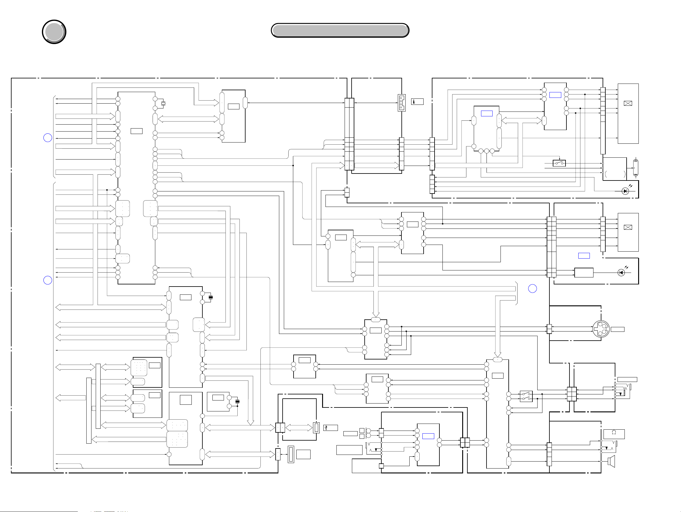
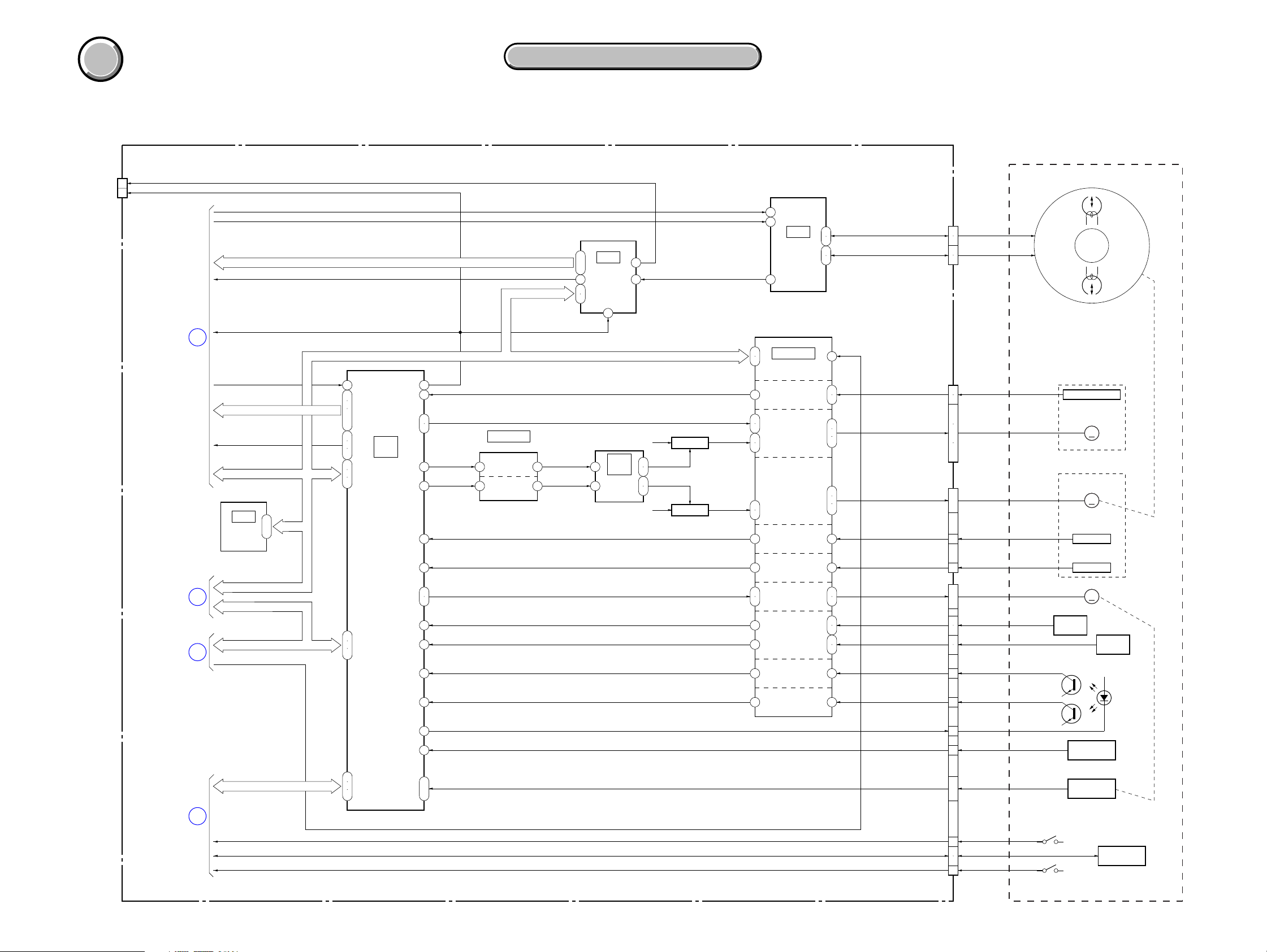
3. BLOCK DIAGRAMS
DCR-PC101/PC101E
3-3. OVERALL BLOCK DIAGRAM (3/4)
VC-284 BOARD (3/4)
CN1006 (2/3)
RF MON
20
CPC
(FOR CHECK)
SWP
17
OVERALL (2/4)
(PAGE 3-3)
RECCK
RECDT
ADDT 0 - 5
PBCK
SWP SWP
4
ATF ERR
MC BUS (10)
FRRV, TRRV, TRRT
VSP SO, VSP SI, XVSP SCK
IC2502
2
(15/20)
ı
4
EEPROM
( ) : Number in parenthesis ( ) indicates the division number of schematic diagram where the component is located.
RECCK
40
RECDT
42
111 164
32
33
45
ı
52
84
IC2501
178
179
67
69
70
(2/2)
MECHA
CONTROL
(15/20)
190
165
166
89
88
197
CAP PWM
DRUM PWM
VSP SO, XVSP SCK
IC2401 (2/2)
(14/20)
(RABI)
41 43
LPF
LPF
44 45
15
IC1901
ADDT 0 - 5
ı
20
PBCK PBYOUT
CAP ERROR
DRUM ERROR
A/D CONV.,
13
22
24
VSP SO, XVSP SCK
CAP FG
CAP ON, CAP FWD
72
78
DRUM FG
EQ,
PLL
(9/20)
31
IC4501
(1/2)
PWM
DRIVE
(18/20)
34
42
UNREG1
26
27
24
25
UNREG1
Q4505, 4516
SWITCHING
SWITCHING
Q4506, 4517
CAP VS
DRUM VS
IC1902
REC/PB AMP
(9/20)
27
36
IC2401 (1/2)
38
(14/20)
CAPSTAN
4
FG AMP
1
80
CAPSTAN
MOTOR
75
DRIVE
77
DRUM
MOTOR
64
DRIVE
67
DRUM
53 52
FG AMP
6
7
1
2
SPCK
35
7
8
74
76
78
63
65
68
ODD
EVEN
FG 1, 2
CAP U, V, W
DRUM U, V, W
DRUM FG SENS
CN1901
CN1009
CN1007
J MECHA DECK
5
6
2
3
22
25
1
ı
4
11
ı
14
17
ı
20
1
ı
6
9
DRUM
M902
CAPSTAN FG
CAPSTAN
MOTOR
MM
M901
DRUM
MOTOR
MM
DRUM FG
OVERALL (2/4)
(PAGE 3-4)
OVERALL (1/4)
(PAGE 3-2)
OVERALL (4/4)
(PAGE 3-8)
5
3
6
VSP SO, XVSP SCK
VD SO, VD SCK
VD SO, VD SI, VD SCK
SPCK
HI SO, HI SI, XHI SCK
REC PROOF
CHIME SDA, CHIME SCK
XCC DOWN
198
13
15
80
82
83
63
65
66
192
193
196
195
180
119
106
ı
108
DRUM PG
LOAD, UNLOAD
TREEL FG
SREEL FG
TAPE END
TAPE TOP
TAPE LED ON
DEW AD
MODE SW A - C
DRUM
50 49
PG AMP
32
LODING MOTOR
33
DRIVE
29
25
21 20
19 20
REEL
FG AMP
TAPE END
DETECT
TAPE TOP
DETECT
69
72
26
27
22
23
DRUM PG SENS
LM±
T REEL±
S REEL±
TAPE END C
TAPE TOP C
CN1008
H902
T REEL
SENSOR
S901
S903
DRUM PG
MM
DEW
SENSOR
S902
MODE
SWITCH
H901
S REEL
SENSOR
TAPE LED
CN901
CASSETTE
MEMORY
M903
LOADING
MOTOR
D901
10
24
ı
27
7
8
4
5
3
1
16
23
19
ı
21
13
11
12
17
Q901
TAPE END
SENSOR
Q902TAPE TOP
SENSOR
REC PROOF
CC DOWN
05
3-5 3-6
DCR-PC101/PC101E
COVER
COVER
3. BLOCK DIAGRAMS
3. BLOCK DIAGRAMS
3-4. OVERALL BLOCK DIAGRAM (4/4)
CONTROL SWITCH BLOCK (FK-2850) (3/3)
S608
BACK LIGHT
S607
DISPLAY/TOUCH PANEL
S604
COLOR SLOW S
SUPER NS
S605
(AF/MF)
FOCUS
(INFINITY)
S606
(INFINITY)
PHOTO
S602
(PHOTO FREEZE)
S603
(PHOTO REC)
NS-014 BOARD CF-089 BOARD
IC701
REMOTE
COMMANDER
RECEIVER
4
D702, 703
(NIGHT SHOT)
LITHIUM
BATTERY
BT001
PD-166 BOARD
(2/2)
TP L, TP R
CN801
(2/2)
15
ı
18
TA901
TOUCH
PANEL
CN802
2
3
TP TOP, TP BOT,
5
6
FP-470 FLEXIBLE BOARD
S4702
(PANEL REVERSE)
S4701
(PANEL OPEN)
BT901
BATTERY
TERMINAL
J901
DC IN
+
S
–
CN001
1
2
3
1
2
3
05
CN002
Q001,
002
Q003,
004
RV601
(ZOOM)
W
S601
RESET
(2/2)
CN104
8
4
1
2
BJ-003 BOARD
(3/3)
CN007
(2/2)
15
ı
18
CN006
KEY AD1
3
KEY AD2
5
CPC
(FOR CHECK)
CN101 (4/4)
CN005 (3/3)
P UNREG
( ) : Number in parenthesis ( ) indicates the division number of schematic diagram where the component is located.
VC-284 BOARD (3/4)
2
5
4
24
16
9
52
52
62
62
54
54
56
56
65
65
66
66
68
68
70
70
3
3
5
5
62
62
61
61
29
29
31
31
30
30
32
32
34
34
36
36
59
59
2
2
ı
ı
16
16
38
38
ı
ı
56
56
CN1004
(3/3)
ZOOM VR AD
KEY AD0
PHOTO FREEZE
HI XRESET
CN1006 (3/3)
HI XRESET
XINIT
CN1001 (4/4)
SIRCS SIG
NS LED K
BATT LI 3V
VTR UNREG
BATT UNREG
CN1003 (3/3)
KEY AD1
KEY AD2
BATT UNREG
BATT SIG
FAST CHARGE
INIT CHARGE ON
VTR UNREG
BATT XEXT
PRT HEAD UNREG,
SHOE PRT UNREG,
UNREG1, UNREG2
D2702
2
D2701
D2704
3
7
INITIAL RESET, BACK UP VCC
Q1002 - 1004
TOUCH
PANEL I/F
VTR DD ON
CAM DD ON
Q1006, 1009
NS LED
DRIVE
PREEND
RESET
VBAT
VIN CS
VOUT
IC2702
(20/20)
BATTERY CHARGE
DETECTOR
BATT UNREG
VTR UNREG
SIRCS PWM
VRO
Q3101
IR ON
5
8
6
4
EVER 3.0V
VOUT
BATT IN
IC4501
(2/2)
DC/DC CONTROL
(18/20)
59
73
47
41
45
31
34
48
71
72
43
42
74
60
61
6
IC3101
HI CONTROL
(16/20)
MT 4.9V
D 2.8V
D 3.1V
D 1.5V
D 1.9V
A 2.8V
GANDHI 1.5V
A 4.6V
CAM 15V
CAM –7.5V
SW 15V
RP 4.6V
RP 2.8V
AU 2.8V
PANEL/EVF 2.8V
PANEL/EVF 13.5V
PANEL/EVF 4.6V
5
28
29
51
52
23
ı
25
35
FAST CHARGE
37
INIT CHARGE ON
38
39
40
57
58
69
4
3
1
2
7
X3101
10MHz
X3102
32.768kHz
TXD0, RXD0, SCK0
VTR DD ON
CAM DD ON
LANC IN,
LANC OUT
185
190
191
168
10
LANC DRIVER
12
SHOE ID 1, 2
SHOE CONT AD
XVTR MODE SW
XCAM MODE SW
XPHOTO STBY SW
HI CONTROL
X EJECT SW
XS/S SW
T
IC2905
(2/2)
(5/20)
IC2703
(20/20)
ZOOM VR AD
XSYS RST
3730
160
162
199
ı
201
205
ı
207
CHIME SDA, CHIME SCK
HI SO, HI SI, XHI SCK
EEP TXD3, EEP RXD3, EEP SCK3
EXT STROBO
CAM DD ON
XCC DOWN
REC PROOF
1
6
IC2906
2
5
EEPROM
6
(5/20)
ME-020 BOARD (4/4)
CN1001 (4/4) CN404 (4/4)
8
221
ı
HS TXD, HS RXD, HS SCK HS TXD, HS RXD, HS SCK
223
11
LANC SIG
8
10
10
12
12
11 11
31 31 13
797
9
13 13 4
28 28
30 30
27 27
26 26
34 34
OVERALL (1/4)
(PAGE 3-1)
OVERALL (3/4)
(PAGE 3-5)
CN402
8
10
12
7
INTELLIGENT
ACCESSORY
SHOE (2/2)
9
11
CONTROL SWITCH BLOCK
(PS-2850)
8
10
4
5
6
(EJECT)
(START/STOP)
OFF (CHARGE)
S4603
POWER
J403
LANC
S4602
S4601
VCR
CAMERA
MEMORY
3-7 3-8
 Loading...