

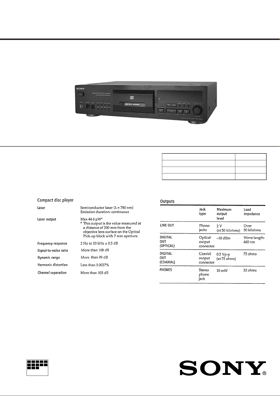
CDP-XB820
SERVICE MANUAL
SPECIFICATIONS
AEP Model
Model Name Using Similar Mechanism NEW
CD Mechanism Type CDM36-14E
Base Unit Type BU-14E
Optical Pick-up Type KSS-213B/F-NP
MICROFILM
– Continued on next page –
COMPACT DISC PLAYER

TABLE OF CONTENTS
1. SERVICING NOTES ............................................... 3
2. GENERAL ................................................................... 6
3. DISASSEMBLY ......................................................... 7
4. TEST MODE
4-1. AF ADJ Mode ................................................................. 9
4-2. ADJ Mode ....................................................................... 10
4-3. CLV-S Mode.................................................................... 10
4-4. AGING Mode.................................................................. 11
5. ELECTRICAL BLOCK CHECKING ................ 12
6. DIAGRAMS
6-1. IC Pin Function Description ........................................... 14
6-2. Note for Printed Wiring Boards and
Schematic Diagrams ....................................................... 16
6-3. Printed Wiring Board – BD Section – ............................ 19
6-4. Schematic Diagram – BD Section – ............................... 21
6-5. Printed Wiring Boards
– OPTICAL PICK-UP/MOTOR Section – .................... 23
6-6. Schematic Diagram
– OPTICAL PICK-UP/MOTOR Section – .................... 24
6-7. Printed Wiring Board – MAIN Section –....................... 25
6-8. Schematic Diagram – MAIN Section (1/2) –................. 27
6-9. Schematic Diagram – MAIN Section (2/2) –................. 29
6-10. Printed Wiring Boards – POWER Section – .................. 31
6-11. Schematic Diagram – POWER Section – ...................... 33
6-12. Printed Wiring Boards – PANEL Section – ................... 35
6-13. Schematic Diagram – PANEL Section –........................ 37
7. EXPLODED VIEWS ................................................ 42
8. ELECTRICAL PARTS LIST ............................... 46
SAFETY-RELATED COMPONENT WARNING!!
COMPONENTS IDENTIFIED BY MARK ! OR DOTTED
LINE WITH MARK ! ON THE SCHEMATIC DIAGRAMS
AND IN THE PARTS LIST ARE CRITICAL TO SAFE
OPERATION. REPLACE THESE COMPONENTS WITH
SONY PARTS WHOSE PART NUMBERS APPEAR AS
SHOWN IN THIS MANUAL OR IN SUPPLEMENTS PUBLISHED BY SONY.
– 2 –
SECTION 1
SERVICING NOTES
NOTES ON HANDLING THE OPTICAL PICK-UP
BLOCK OR BASE UNIT
The laser diode in the optical pick-up block may suffer electrostatic break-down because of the potential difference generated
by the charged electrostatic load, etc. on clothing and the human
body.
During repair, pay attention to electrostatic break-down and also
use the procedure in the printed matter which is included in the
repair parts.
The flexible board is easily damaged and should be handled with
care.
NOTES ON LASER DIODE EMISSION CHECK
The laser beam on this model is concentrated so as to be focused
on the disc reflective surface by the objective lens in the optical
pick-up block. Therefore, when checking the laser diode emission, observe from more than 30 cm away from the objective lens.
Notes on chip component replacement
• Never reuse a disconnected chip component.
• Notice that the minus side of a tantalum capacitor may be damaged by heat.
CAUTION
Use of controls or adjustments or performance of procedures
other than those specified herein may result in hazardous radiation exposure.
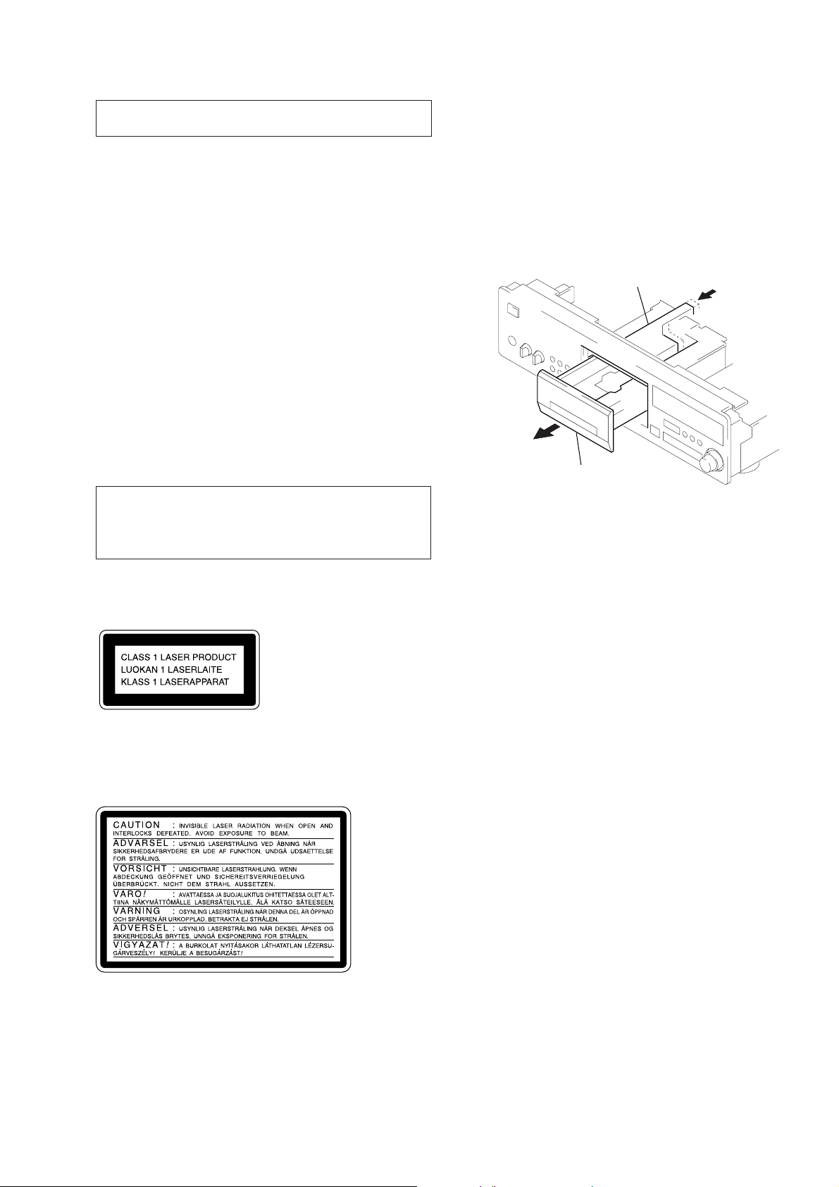
HOW TO OPEN THE DISC TRAY WHEN POWER
SWITCH TURNS OFF
Insert a tapering driver into the aperture of he unit bottom, and
turn in the direction of arrow (to OUT direction).
DISC REMOVAL PROCEDURE (at POWER OFF)
1. Remove the case. (Refer to page 7.)
2. Push the slide cam in the direction of the arrow A.
3. Draw out the loading panel in the direction of the arrow B by
hand, and remove a disk.
slide cam
A
”B
loading panel
This appliance is classified as a CLASS 1 LASER product.
The CLASS 1 LASER PRODUCT MARKING is located on
the rear exterior.
Laser component in this product is capable of emitting radiation
exceeding the limit for Class 1.
The following caution label is located inside the unit.
– 3 –
CD-TEXT TEST DISC
This unit is able to display the test data (character information) written in the CD on its fluorescent indicator tube.
The CD-TEXT TEST DISC (TGCS-313:4-989-366-01) is used for checking the display.
To check, perform the following procedure.
Checking Method:
1. Turn ON the power, set the disc to the disc table with the “test disc” label facing up, and chuck the disc.
2. Press the · button and play back the disc.
3. The following will be displayed on the fluorescent indicator tube.
Display : 1KHZ 0DB
4. Rotating [AMS] knob, select the track. The text data of each track will be displayed.
For details of the displayed contents for each track, refer to “Table 1 : CD-TEXT TEST DISC TEXT Data Contents” and “Table 2 : CDTEXT TEST DISC Recorded Contents and Display”.
Restrictions in CD-TEXT Display
In this unit, some special characters will not be displayed properly. These will be displayed as a space or a character resembling it. For
details, refer to “Table 2 : CD-TEXT DISC Recorded Contents and Display”.
Table 1 : CD-TEXT TEST DISC TEXT Data Contents (TRACKS No. 1 to 41:Normal Characters)
TRACK
≠
No.
1 1kHz/0dB/L&R 22 1kHz/-90dB/L&R
2 20Hz/0dB/L&R 23 Infinity Zero w/o emphasis//L&R
3 40Hz/0dB/L&R 24 Infinity Zero with emphasis//L&R
4 100Hz/0dB/L&R 25 400Hz+7kHz(4:1)/0dB/L&R
5 200Hz/0dB/L&R 26 400Hz+7kHz(4:1)/-10dB/L&R
6 500Hz/0dB/L&R 27 19kHz+20kHz(1:1)/0dB/L&R
7 1kHz/0dB/L&R 28 19kHz+20kHz(1:1)/-10dB/L&R
8 5kHz/0dB/L&R 29 100Hz/0dB/L*
9 7kHz/0dB/L&R 30 1kHz/0dB/L*
10 10kHz/0dB/L&R 31 10kHz/0dB/L*
11 16kHz/0dB/L&R 32 20kHz/0dB/L*
12 18kHz/0dB/L&R 33 100Hz/0dB/R*
13 20kHz/0dB/L&R 34 1kHz/0dB/R*
14 1kHz/0dB/L&R 35 10kHz/0dB/R*
15 1kHz/-1dB/L&R 36 20kHz/0dB/R*
16 1kHz/-3dB/L&R 37 100Hz Squer Wave//L&R
17 1kHz/-6dB/L&R 38 1kHz Squer Wave//L&R
18 1kHz/-10dB/L&R 39 1kHz w/emphasis/-0.37dB/L&R
19 1kHz/-20dB/L&R 40 5kHz w/emphasis/-4.53dB/L&R
20 1kHz/-60dB/L&R 41 16kHz w/emphasis/-9.04dB/L&R
21 1kHz/-80dB/L&R
±
Displayed Contents
TRACK
No.
Displayed Contents
NOTE: The contents of Track No. 1 to 41 are the same as those of the current TEST DISC-their titles are displayed.
– 4 –
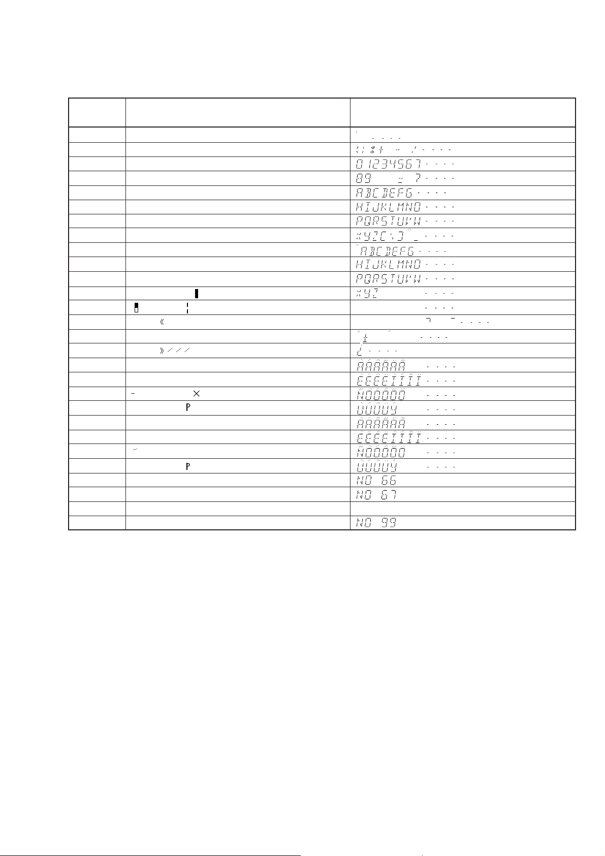
Table 2: CD-TEXT TEST DISC Recorded Contents and Display
(In this unit, some special characters cannot be displayed. This is no a fault.)
TRACK
No.
42
43
44
45
46
47
48
49
50
51
52
53
54
55
56
57
58
59
60
61
62
63
64
65
66
67
to
99
Recorded contents
! ” # $ %& ´ (21h to 27h)1kHz 0dB L&R
( ) + , – . / (28h to 2Fh)
*
01234567 (30h to 37Fh)
8 9 : ; < = > ? (38h to 3Fh)
@A B C D E F G (40h to 47Fh)
H I J K L MNO (48h to 4Fh)
P QR S T U VW (50h to 57Fh)
X Y Z [ ¥ ] ^ _ (58h to 5Fh)
a b c d e f g (60h to 67Fh)
′
h i j k l m n o (68h to 6Fh)
p q r s t u v w (70h to 77Fh)
xyz{ I }
~
(78h to 7Fh)
i¢£¤¥ § (A0h to A7h) 8859-1
¬
≥ C ª
•±23
1
º ¿ (B8h to BFh)
†
–
PR
µ ¶ • (B0h to B7h)
′
14123
(A8h to AFh)
4
АБВГДЕЖЗ (C0h to C7Fh)
ИЙКЛМНОП (C8h to CFh)
D СТУФХЦ
ШЩЪЫЬY
˙
(D0h to D7Fh)
Я (D8h to DFh)
абвгдежз (E0h to E7Fh)
ийклмноп (E8h to FFh)
∂ стуфхц÷ (F0h to F7Fh)
шщъыьy
ÿ (F8h to FFFh)
´
No.66
No.67
to
No.99
Display
to
– 5 –
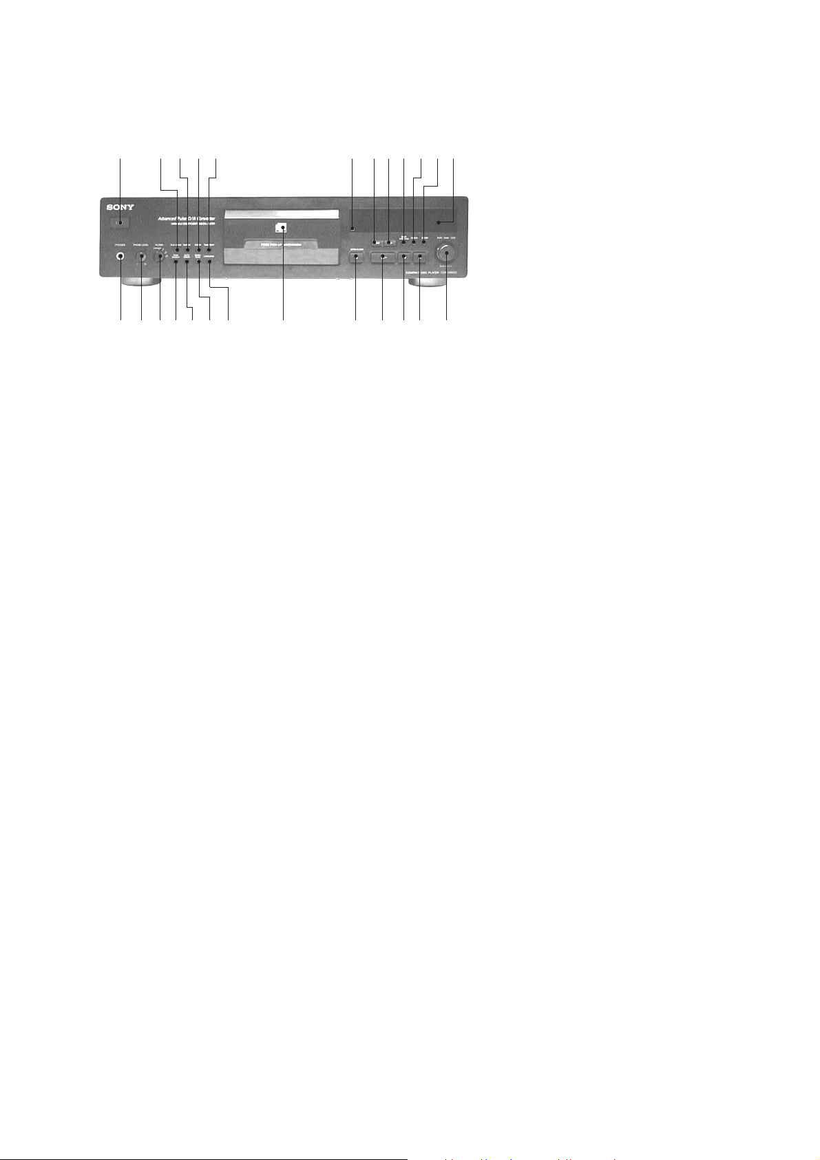
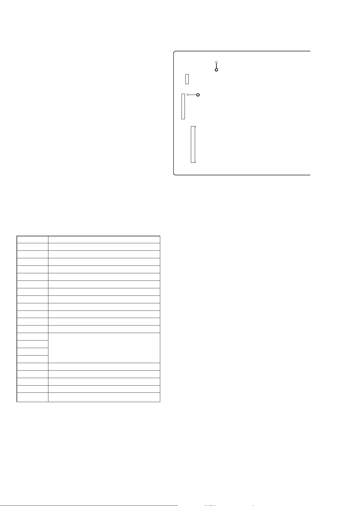
• LOCATION OF CONTROLS
SECTION 2
GENERAL
1 432 5 6
!£ !¢ !∞!§ !¶ !• !ª @º @¡ @™ @£@¢ @∞
1 U (power) button
2 PLAY MODE button
3 REPEAT button
4 FADER button
5 TIME TEXT button
6 Remote sensor
7 0 button
8 ) button
9 EDIT/TIME FADER button
0 CHECK button
!¡ CLEAR button
!™ Fluorescent indicator tube
!£ PHONES jack
!¢ PHONE LEVEL knob
!∞ FILTER knob
!§ PEAK SEARCH button
!¶ AUTO SPACE button
!• MUSIC SCAN button
!ª LANGUAGE button
@º Disc tray
@¡ § OPEN/CLOSE button
@™ · button
@£ P button
@¢ p button
@∞ ≠ AMS ±, PUSH ENTER knob
78
9 0 !¡!™
– 6 –
SECTION 3
)
DISASSEMBLY
Note: Follow the disassembly procedure in the numerical order given.
CASE
2
two screws
(case 3TP2)
2
two screws
(case 3TP2)
3
case
1
two screws
(BV/RING)
2
two screws
(case 3TP2)
FRONT PANEL SECTION
2
two claws
3
loading panel ass’y
8
claw
1
Push the slide cam
in the direction of the arrow
A
4
connector
(CN903)
A
.
5
connector
(CN351)
6
flat wire (25 core
(CN302)
9
front panel section
– 7 –
8
claw
7
five screws
(BV3
×
8)
MECHANISM DECK (CDM36-14E)
k
2
screw
(BVTP3
3
lug
1
4
two screws
(BVTP3
×
8)
flat wire (23 core)
(CN301)
4
two screws
×
8)
(BVTP3
×
8)
5
mechanism dec
(CDM36-14E)
MAIN BOARD
4
two screws
(BVTP 3
2
connector
(CN951)
4
1
flat wire (23 core)
(CN301)
×
8)
two screws
(BVTP 3
5
main board
×
8)
3
four screws
(BV/RING)
– 8 –
SECTION 4
TEST MODE
4-1. AF ADJ MODE
The following checks can be performed in the AF ADJ mode, which
is set by connecting the TP2 (AF ADJ : JW96) terminal on MAIN
board to the Ground and turning on the power.
• FL tube check
After all segments light up, when the · button is pressed, the
following will be displayed. (Partial lighting 1)
(Partial lighting 1)
When the p button is pressed, the following will be displayed.
(partial lighting 2)
24
6810
12 14
16 18 20
When the OPEN/CLOSE § button is pressed, all will light up
again.
When the ≠ AMS ± knob is rotated, the following
will be displayed. (partial lighting 3)
(Partial lighting 2)
Buttons and Corresponding Button Numbers
Button Button Number or Display
LANGUAGE 0
MUSIC SCAN 1
AUT O S PAC E 2
PEAK SEARCH 3
PLAY MODE 4
REPEAT 5
FADER 6
TIME/TEXT 7
0 8
) 9
EDIT/TIME FADE 10
CHECK 11
CLEAR 12
P 18
PUSH ENTER 20
OPEN/CLOSE § All lit
PLAY · Partial lighting 1
STOP p Partial lighting 2
≠ AMS ± Partial lighting 3
“FILTER-STD/1/2/3” is displayed on the FL tube when the
FILTER switch is pressed.
Rightward:
Lefrward:
(Partial lighting 3)
• Key check
All buttons have corresponding b utton numbers. When a button is
pressed, the counter will count up and display the button’s number. Ho wever , the counter will only count to “18”. It will not count
for buttons already pressed once, but will display the button’ s number.
Â
Display of counting
Display of button number
Â
• Remote commander check
“REMOCON PLA Y” is displayed on the FL tube when the PLAY
button on the remote commander is pressed.
All go off when the other buttons a pressed.
• Audio check
• Initial setting of digital filter and release of mute.
• When the TP2 (AF ADJ) terminal on MAIN board is set to HIGH
(VDD), emphasis turns on. When set to LOW (GND), it turns
off.
– 9 –
4-2. ADJ MODE
The following operations are performed in the ADJ mode, which
is set by connecting the TP1 (ADJ : JW98) terminal to the Ground
and turning on the power.
• During playback, there is no problem even if the GFS is continuously LOW.
• High speed search is prohibited during access.
• During playback, the gain of focus servo and spindle servo does
not decrease.
• Servo related manual operations and measurement can be
performed.
(For details of operations, refer to Table of Key Operrations in
ADJ Mode.)
[ MAIN BOARD ] – Conductor Side –
JW096
IC930
TP2
(AFADJ)
JW098
TP1
(ADJ)
IC302
4-3. CLV-S MODE
The spindle servo for playback sets into the CLV-S mode when
the TP2 (AF ADJ) terminal is connected to Ground after turning on
the power.
T ABLE OF BUTTON OPERATIONS IN ADJ MODE
The jitter value display mode can be set after the all-music
remaining number mode using the [TIME/TEXT] button.
The functions of the number buttons are shown in the following
table.
FUNCTIONS OF NUMBER BUTTONS
(With the attached remote commander)
Button Function
1 Focus bias up
2 Focus bias aliasing (upper, middle, lower) display
3 Focus bias (best point, jitter value) display
4 Tracking servo, sled servo off
5 Tracking gain up
6 Focus bias down
7 Focus bias readjustment
8 Focus bias 00 point
9 Tracking servo, sled servo on
10 Tracking gain normal
11 S-Curve mode (play mode only)
12 Eccentric mode
13
14
15
16
17 Tracking gain initialize
18 Offset display (TE), EF, Bias
19 Offset display (VC, FE, RF)
20 Auto gain (FCS, TRK)
CLR key (Error Rate, RFCK, GFS) selection
Reserved for BD
CN302
– 10 –
4-4. AGING MODE
1. How to Enter AGING Mode
Aging method 1
(When using the aging mode remote controller (J-2501-123-A)):
1) Pess the U button and turn ON the power.
2) Set the disc on the tray.
3) Press the [AGINGSTART] button of the aging remote control-
ler.
4) Aging starts and the message shown in Fig. 1 is displayed on the
fluorescent display tube.
5) To end, press the U button.
Aging method 2 (When no aging mode remote controller):
1) Turn on the power of the set, and insert any disc.
2) Press three buttons of [MUSICSCAN], [ªOPEN/CLOSEº],
and p simultaneously, and the set goes in the AGING mode.
3) Performing the aging for a while, confirm that “ERROR” is not
displayed on the fluorescent display tube.
2. How to Exit from AGING Mode
Turn off the Power, and normal operation becomes ready.
3. Operation sequence in AGING Mode.
Contents of AGING mode
Display Operation
1 AGING-0 loading IN
2 AGING-1 Toc read
3 AGING-2 last access
4 AGING-3 last play
5 AGING-4 first access
6 AGING-5 first play
7 AGING-6 loading OUT
§
Fig. 1
*: In case of a failure
A faulty operation mode No. such as “ERROR-3’’ is blinking.
*: During aging, the keys on the set and the remote control A1 are
not accepted.
*: To quit the aging, turn of the power of the set.
– 11 –
SECTION 5
V
)
ELECTRICAL BLOCK CHECKING
Note:
1. CD Block is basically designed to operate without adjustment. Therefore, check each item in order given.
2. Use YEDS-18 disc (3-702-101-01) unless otherwise indicated.
3. Use an oscilloscope with more than 10MΩ impedance.
4. Clean the object lens by an applicator with neutral detergent when the
signal level is low than specified value with the following checks.
S Curve Check
Connection:
oscilloscope
BD board
TP2 (FE)
TP (VC)
+
–
Procedure :
1. Connect oscilloscope to test point TP2 (FE) on BD board.
2. Connect between test point TP3 (FEI) and TP (VC) by lead wire.
3. Turn ON the power.
4. Put disc (YEDS-18) in and turned Power switch on again and
actuate the focus search. (actuate the focus search when disc
table is moving in and out.)
5. Check the oscilloscope waveform (S-curve) is symmetrical
between A and B. And confirm peak to peak level within 3±1
Vp-p.
S-curve waveform
symmetry
A
B
within 3
±
1 Vp-p
6. After check, remove the lead wire connected in step 2.
Note : • Try to measure several times to make sure than the ratio of A : B
or B : A is more than 10 : 7.
• Take sweep time as long as possible and light up the
brightness to obtain best waveform.
Note: A clear RF signal waveform means that the shape “≈” can be clearly
distinguished at the center of the waveform.
RF signal waveform
VOLT/DIV: 200 m
TIME/DIV: 500 ns
level: 1.2
±
0.2 Vp-p
E-F Balance (1 Track Jump) Check
(Without remote commander)
Connection:
oscilloscope
(DC range)
BD board
TP4 (TE)
TP (VC)
+
–
Procedure :
1. Connect oscilloscpe to test point TP4 (TE) on BD board.
2. Turn ON the power.
3. Put disc (YEDS-18) in to play the number five track.
4. Press the “P (Pause)” button. (Becomes the 1 track jump mode)
5. Check the level B of the oscilliscope's waveform and the A (DC
voltage) of the center of the Traverse waveform.
Confirm the following :
A/B x 100 = less than ± 22%
1 track jump waveform
Center of the waveform
B
0 V
A (DC voltage
RF Level Check
Connection:
oscilloscope
BD board
TP1 (RF)
TP (VC)
+
–
Procedure :
1. Connect oscilloscope to test point TP1 (RF) on BD board.
2. Turn ON the power.
3. Put disc (YEDS-18) in to play the number five track.
4. Confirm that oscilloscope waveform is clear and check RF signal level is correct or not.
level: 1.3 ± 0.6 Vp-p
symmetry
E-F Balance Check (With remote commander)
Connection:
oscilloscope
(DC range)
BD board
TP4 (TE)
TP (VC)
+
–
Procedure :
1. Connect the test point TP1 (ADJ : JW98) on MAIN board to the
ground with a lead wire on MAIN board.
2. Connect oscilloscpe to test point TP4 (TE) on BD board.
3. Turn ON the power to set the ADJ mode.
4. Put disc (YEDS-18) in to play the number five track.
5. Press the “4” button. (The tracking servo and the sledding servo
are turned OFF.)
– 12 –
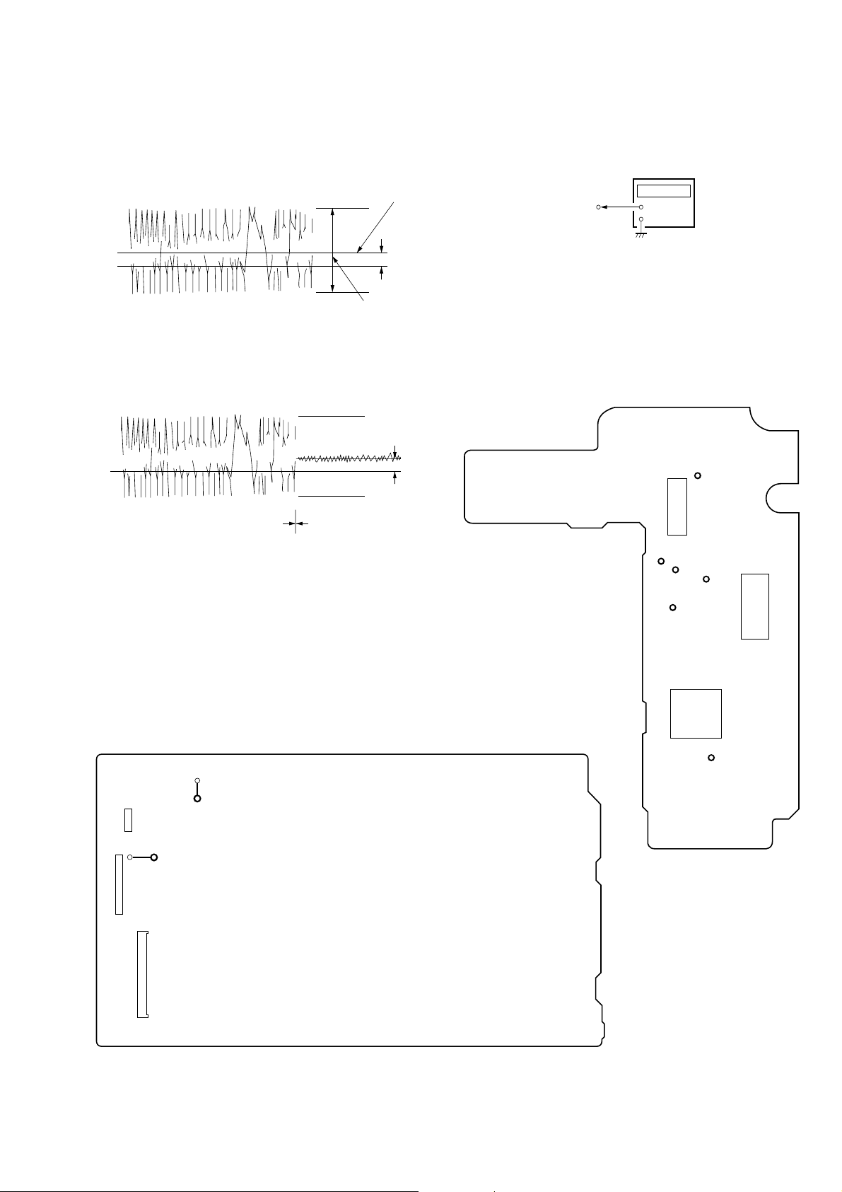
6. Check the lev el B of the oscilliscope's wa v eform and the A (DC
)
r
voltage) of the center of the Traverse waveform.
Confirm the following :
A/B x 100 = less than ± 22%
Traverse waveform
Center of the waveform
B
RF PLL Free-run Frequency Check
Procedure :
1. Connect frequency counter to test point (MNT1) with lead wire.
frequency counte
BD board
TP9 (MNT1)
+
–
0 V
A (DC voltage)
level: 1.3
±
0.6 Vp-p
7. Press the “9” button. (The tracking serv o and sledding servo are
turned ON.) Confirm the C (DC voltage) is almost equal to the A
(DC voltage) is step 6.
Traverse waveform
0 V
Tracking servo
Sledding servo
OFF
Tracking servo
Sledding servo
ON
8. Disconnect the lead wire of TP1 (ADJ : JW98) connected in
step 1.
C (DC
voltage
2. Turn ON the power.
3. Put the disc (YEDS-18) in to play the number five track.
Confirm that reading on frequency counter is 4.3218MHz.
Adjustment Location :
[ BD BOARD ] — Side A —
TP
IC103
TP4
(TE)
TP2
(FE)
TP1
(RF)
(VC)
TP3
(FEI)
IC102
[ MAIN BOARD ] – Conductor Side –
JW096
IC930
TP2
(AFADJ)
JW098
TP1
(ADJ)
IC302
CN302
IC101
TP9
(MNT1)
– 13 –

SECTION 6
DIAGRAMS
6-1. IC PIN FUNCTION DESCRIPTION
• DISP BOARD IC801 CXP82832-009Q (SYSTEM CONTROLLER/FL DRIVER)
Pin No. Pin Name I/O Function
1, 2
3
4
5 SCOR
6, 7
8
9
10, 11
12
13
14
15
16
17
18
19
20
21
22 CLK O
23
24
25
26
27
28 AVREF I
29
30
31
32
33
34
35
13G, 14G O Grid drive signal output to the fluorescent indicator tube (FL801) “H”: goes on
NC — Not used (fixed at “H”)
+5V — Power supply terminal (+5V)
Subcode sync (S0+S1) detection signal input from the CXD2585Q (IC101) in BD section
I
“H” active
GND — Ground terminal
RMIN I Sircs signal input from the remote control receiver (IC802) “L” active
GND — Ground terminal
OPEN O Not used (open)
LDOUT O
LDIN
SENSE I Internal status monitor input from the CXD2585Q (IC101) in BD section
XLT O Serial data latch pulse output to the CXD2585Q (IC101) in BD section “L” active
DMUTE O
PRGLT O Serial data latch pulse output to the D/A converter (IC301) “L” active
SENSOR IN I Stabilizer detect sensor input terminal (fixed at “L” in this set)
BUSOUT O Sircs remote control signal output for the CONTROL A1 “H” active
BUSIN I Sircs remote control signal input for the CONTROL A1 “L” active
SENSOR SW I Stabilizer detect sensor switch input terminal “H” active Not used (open)
LDON O Laser on/off control signal output to the CXA2568M (IC103) “H”: laser on
DATA
SQCK
SUBQ
+5V — Power supply terminal (+5V)
KEY0 I
KEY1 I
KEY2 I
FILTER.SW I FILTER switch (S860) input terminal (A/D input)
ADJ/AFADJ I
LOADSW I Loading in/out detect switch (S152 and S153) input terminal
MODEL.SEL1 I Destination setting terminal (fixed at “H”)
Motor control signal (load out direction) output to the loading motor driver (IC302)
“H” active *1
Motor control signal (load in direction) output to the loading motor driver (IC302)
O
“H” active *1
Digital muting on/off control signal output to the CXD2585Q (IC101) and D/A converter (IC301)
“L”: muting on
Serial data transfer clock signal output to the CXD2585Q (IC101) in BD section “L” active
O
Serial data output to the CXD2585Q (IC101) in BD section
Subcode Q data reading clock signal output to the CXD2585Q (IC101) in BD section
O
“L” active
I
Subcode Q data input from the CXD2585Q (IC101) in BD section
Reference voltage (+5V) input terminal (for A/D converter)
Key input terminal (A/D input) S851 to S858 (LANGUAGE, MUSIC SCAN, AUTO SPACE,
PEAK SEARCH, PLAY MODE, REPEAT, FADER, TIME/TEXT keys input)
Key input terminal (A/D input) S801 to S805 and S810 (CLEAR, CHECK, EDIT/TIME FADE,
0, ), PUSH ENTER keys input)
Key input terminal (A/D input)
S806 to S810 (§ OPEN/CLOSE, ·, P, p, ≠ AMS ± keys input)
Input terminal for the CD test mode setting
“L”: ADJ mode, center voltage: AFADJ mode, normally: “H”
*1 Loading motor (M903) control
Operation
Terminal
LDOUT (pin !™)
LDIN (pin !£)
IN OUT BRAKE RUN IDLE
“L” “H” “H” “L”
“H” “L” “H” “L”
– 14 –

Pin No. Pin Name I/O Function
36
37 AVSS
38
39
40
41
42
43
44
45
46
47
48
49 to 66
67 to 87
88
89
90 to 100
MODEL.SEL2 I Destination setting terminal (fixed at “L”)
— Ground terminal (for A/D converter)
System reset signal input from the reset signal generator (IC930) “L”: reset
RST
EXTAL I Main system clock input terminal (8 MHz)
XTAL O Main system clock output terminal (8 MHz)
VSS — Ground terminal
TX O Sub system clock output terminal Not used (open)
TEX I Sub system clock input terminal Not used (fixed at “L”)
VDD (+5V) — Power supply terminal (+5V)
VFDP (–30V) — Power supply terminal (–30V) (for FL drive)
XSEL O Not used (open)
REINIT O Not used (open)
RFGF O Laser power hold control signal output to the CXA2568M (IC103) “H”: hold on
OPEN O Not used (open)
S21 to S1 O Segment drive signal output to the fluorescent indicator tube (FL801) “H”: goes on
1G O Grid drive signal output to the fluorescent indicator tube (FL801) “H”: goes on
VDD (+5V) — Power supply terminal (+5V)
2G to 12G O Grid drive signal output to the fluorescent indicator tube (FL801) “H”: goes on
I
For several hundreds msec. after the power supply rises, “L” is input, then it changes to “H”
– 15 –

6-2. NOTE FOR PRINTED WIRING BOARDS AND SCHEMATIC DIAGRAMS
Note on Schematic Diagram:
• All capacitors are in µF unless otherwise noted. pF: µµF
50 WV or less are not indicated except for electrolytics
and tantalums.
• All resistors are in Ω and 1/
specified.
¢
•
: internal component.
4
W or less unless otherwise
• 5 : fusible resistor.
• C : panel designation.
Note: The components identified by mark ! or dotted line
with mark ! are critical for safety.
Replace only with part number specified.
• U : B+ Line.
• V : B– Line.
• Voltages and wa vef orms are dc with respect to ground in
playback mode.
no mark : PLAY
• Voltages are taken with a VOM (Input impedance 10 M Ω).
Voltage variations may be noted due to normal production tolerances.
• Waveforms are taken with a oscilloscope.
Voltage variations may be noted due to normal production tolerances.
• Circled numbers refer to waveforms.
• Signal path.
J : CD
c : digital out
Note on Printed Wiring Boards:
• X : parts extracted from the component side.
®
•
: Through hole.
• b : Pattern from the side which enables seeing.
(The other layers' patterns are not indicated.)
Caution:
Pattern face side: Parts on the pattern face side seen from
(Side B) the pattern face are indicated.
Parts face side: Parts on the parts face side seen from
(Side A) the parts face are indicated.
• Indication of transistor.
C
Q
B
E
These are omitted.
Q
B
CE
These are omitted.
– 16 –

• Circuit Boards Location
AC SW board
HP board
VC SELECT board
TRANS board
BD board
LOADING board
SLED board
MAIN board
KEY board
SPINDLE board
DISP board
– 17 –

• Wavef orms
– BD Board –
1 IC103 !§ (RFO) (PLAY MODE)
500 mV/DIV, 1 µs/DIV
2 IC101 $¡ (TE) (PLAY MODE)
200 mV/DIV, 1 µs/DIV
3 IC101 #ª (FE) (PLAY MODE)
100 mV/DIV, 500 ns/DIV
1.2 ± 0.2 Vp-p
Approx.
570 mVp-p
6 IC101 0 (WFCK)
2 V/DIV, 100 µs/DIV
µ
s
136
7 IC101!™ (XPCK)
2 V/DIV, 100 ns/DIV
230 ns
5.8 Vp-p
6.6 Vp-p
4 IC101^∞ (LRCK)
2 V/DIV, 10 µs/DIV
22.8
5 IC101 ^¶ (BCLK)
2 V/DIV, 200 ns/DIV
– MAIN Board –
Approx.
240 mVp-p
5.8 Vp-p
1 IC301 @• (XOUT)
2 V/DIV, 20 ns/DIV
3.4 Vp-p
45 MHz
– DISP Board –
1 IC801 #ª (EXTAL)
2 V/DIV, 50 ns/DIV
µ
s
4.2 Vp-p
472
5.8 Vp-p
µ
s
8 MHz
– 18 –

CDP-XB820
6-3. PRINTED WIRING BOARD – BD Section – • See page 17 for Circuit Boards Location.
(Page 23)
(Page 23)
• Semiconductor
Location
Ref. No. Location
D101 E-4
IC101 D-3
IC102 C-4
IC103 B-3
Q101 A-3
Q102 A-3
(Page 25)
– 19 –
– 20 –

6-4. SCHEMATIC DIAGRAM – BD Section – • See page 18 for Waveforms. • See page 39 and 40 for IC Block Diagrams.
CDP-XB820
(Page 24)
(Page 27)
(Page 24)
– 21 –
– 22 –

CDP-XB820
6-5. PRINTED WIRING BO ARDS – OPTICAL PICK-UP / MO TOR Section –
• See page 17 for Circuit Boards Location.
(Page 20)
6-6. SCHEMATIC DIAGRAM – OPTICAL PICK-UP / MOTOR Section –
(Page 23)
(Page 22)
(Page 23)
(Page 20)
(Page 22)
The components identified by mark ! or dotted
line with mark ! are critical for safety.
Replace only with part number specified.
– 23 –
– 24 –

6-7. PRINTED WIRING BOARD – MAIN Section – • See page 17 for Circuit Boards Location.
CDP-XB820
(Page 36)
• Semiconductor Location
Ref. No. Location
D301 C-1
D303 D-5
D304 D-6
D305 E-6
D381 E-8
D909 B-3
D910 C-7
D911 D-3
D912 C-3
IC301 B-4
IC302 C-1
Ref. No. Location
IC303 D-6
IC371 D-8
IC391 D-8
IC401 A-6
IC501 B-6
IC901 D-4
IC902 D-4
IC903 D-4
IC904 D-3
IC905 C-3
IC930 A-1
Ref. No. Location
Q301 D-5
Q381 E-8
Q401 A-8
Q402 A-8
Q404 D-5
Q405 D-7
Q501 B-8
Q502 B-8
Q504 E-5
Q505 D-6
Q901 C-4
Q902 E-3
(Page 20)
(Page 31)
(Page 26)
(Page 26)
– 25 –
– 26 –

CDP-XB820
6-8. SCHEMATIC DIAGRAM – MAIN Section (1/2) – • See page 18 for Waveform. • See page 41 for IC Block Diagrams.
(Page 21)
(Page 38)
(Page 29)
– 27 –
– 28 –

6-9. SCHEMATIC DIAGRAM – MAIN Section (2/2) –
CDP-XB820
(Page 33)
(Page 28)
– 29 –
– 30 –

CDP-XB820
6-10. PRINTED WIRING BOARDS – POWER Section – • See page 17 for Circuit Boards Location.
(Page 25)
(Page 31)
– 31 –
(Page 32)
– 32 –

6-11. SCHEMATIC DIAGRAM – POWER Section –
CDP-XB820
(Page 30)
The components identified by mark ! or dotted
line with mark ! are critical for safety.
Replace only with part number specified.
– 33 –
– 34 –

CDP-XB820
6-12. PRINTED WIRING BOARDS – PANEL Section – • See page 17 for Circuit Boards Location.
(Page 35)
(Page 36)
(Page 25)
– 35 –
– 36 –

6-13. SCHEMATIC DIAGRAM – PANEL Section – • See page 18 for Waveform.
CDP-XB820
(Page 27)
– 37 –
– 38 –

• IC Block Diagrams
– BD BOARD –
IC101 CDX2585Q
EXCK
SCSY
SBSO
80
79 77
78
1
DVDD0
2
XRST
MUTE
3
4
DATA
5
XLAT
CLOCK
SENS
SCLK
ATSK
WFCK
XUGF
6
7
8
9
10
11
CPU
Interface
SQCK
76
SQSO
XOLT
7475 73
SOCK
SOUT
D/A
Interface
Sub Code
Processor
Sequencer
Servo
Auto
Error
Corrector
XTAO
72
XTAI
70
71
Clock
Generator
EFM
demodurator
DVSS2
69
XTSL
32K
RAM
68
EMPH
67
BCK
66 65
LRCK
PCMD
Digital
PLL
Asymmetry
Corrector
DOUT
64
Digital
OUT
63
MD2
ASYE
62 61
DVDD2
60
59
58
57
56
55
54
53
52
51
50
49
VPCO
V16M
VCTL
BIAS
AVDD1
PCO
FILI
FILO
CLTV
AVSS1
RFAC
ASYI
XPCK
GFS
V2PO
SCOR
C4M
WDCK
DVSS0
COUT
MIRR
12
48
13
Digital
2423
PWMI
25 26
LOCK
CLV
MDP
27
SSTP
28
FETO
29
SFDR
DVDD1
30
31
11
SRDR
PWM GENERATOR
FORCUS PWM
TRACKING PWM
32
33 34
11
FFDR
TFDR
TRDR
GENERATOR
GENERATOR
SLED PWM
GENERATOR
FRDR
SIGNAL PROCESSOR BLOCK
SERVO BLOCK
SERVO DSP
FOCUS SERVO
TRACKING
SERVO
SLED SERVO
OPAmp
A/D
TEST
TES1
Analog SW
38 39 40
VC
Converter
35 36 37
DVSS1
FE
SE
14
15
16
17
18
19
20
SERVO
Interface
MIRR
DFCT
FOK
21
22
FOK
DFCT
47
46
45
44
43
42
41
ASYO
AVDD0
IGEN
AVSSO
ADIO
RFDC
CE
TE
– 39 –

IC103 CXA2568M-T6
HOLD
AGC VTH
VEE
+
–
VC
VCC
APC LD AMP
50µA
+
–
+
–
VEE
RF SUMMING AMP
VC
+
–
FOCUS ERROR AMP
+
–
VCC
+
–
VCC
VC
+
–
VC
RF EQ AMP
+
–
+
–
1
VEE
2
LD
3
4
PD
5
A
6
B
C
7
D
8
9
VC
10
F
APC PD AMP
+
–
+
–
VEE
–
+
VC
VEE
VC
+
–
24
23
22
21
20
19
18
17
16
15
14
VCC
LC/PD
LD ON
HOLD SW
AGC CONT
RF BOT
RFTC
RF I
RF O
RFE
FE
–
+
VC BUFFER
VC
–
+
VC
+
–
VEE
VCC
E
11
VC
VC
12
VC
TRACKING
ERROR AMP
TE
13
– 40 –

– MAIN Board –
IC301 CXD8735N
INVO
BCKI
DATA1
LRCKI
INIT
ATT
SHIFT
LATCH
SYSM
DVSS1
DVDD1
CKCTL
MUTE
SYNC
VSUB
AVDDL1
L1(–)
L1(+)
AVSSL1
1
2
3
4
5
6
7
8
9
10
NU
11
NU
12
13
14
NU
15
16
17
18
19
20
21
22
S/P
MODE
ATT
IIR
ATT
IIR
3rd order
NOISE
SHAPER
REGISTER
3rd order
NOISE
SHAPER
Buffer(–) PLM-L1
Buffer(+)
OVERFLOW DETECTER OR
FIR1
FIR1
FIR2
FIR4
OVERFLOW DETECTER
FIR2
FIR4
L.I.P
DITHER
L.I.P
X0.75
X0.75
FIR3
FIR3
ATT
ATT
PLM-R1
CLOCK
GENERATOR
D/F
TIMNG
Buffer(–)
Buffer(+)
CIRCUIT
CLOCK
MUTE
CIRCUIT
“0” DETECT
BUFFER
56
55
54
53
52
51
50
49
48
47
46
45
44
43
42
41
40
39
38
37
36
35
INVI
TEST
128FsO
DINIT
OVFLAG
MUTEL
MUTER
NU
64FSI
MCKIN
DVSS1
DVDD1
DVDD2
256FSO
CKVdd
LVCKO
64FSO
DVSS2
AVDDR1
R1(–)
R1(+)
AVSSR2
23
AVSSL2
L2(+)
L2(–)
AVDDL2
XVDD
XVDD
24
25
26
27
28
Buffer(+)
Buffer(–)
1024Fs-CLOCK
BUFFER
PML-L2
IC302 LB1641
T.S.D O.C.P
MOTOR
DRIVE
FWD/REV/STOP
CONTROL LOGIC
2 3
1
GND
DRIVE
MOTOR
NOISE
FILTER
5 6 7 8 9 10
4
VCC 1
FWD.IN
REV.IN
CLAMP
VCC 2
MOTOR
NOISE
FILTER
DRIVE
PLM-R2
DRIVE
MOTOR
Buffer(+)
Buffer(–)
IC930 M51957AL
–
+
1.25V
1 2
VDD
3
IN
GND
AVSSR2
34
R2(+)
33
R2(–)
32
31
AVDDR2
30
XVSS
29
XIN
4
DL
5
OUT
– 41 –

SECTION 7
EXPLODED VIEWS
NOTE:
• -XX and -X mean standardized parts, so they
may have some difference from the original
one.
• Color Indication of Appearance Parts
Example:
KNOB, BALANCE (WHITE) . . . (RED)
↑↑
Parts Color Cabinet's Color
(1) FRONT PANEL SECTION
10
10
9
8
supplied
with J601
supplied
with RV601
15
26
7
6
5
12
not supplied
• Items marked “*” are not stocked since they
are seldom required for routine service. Some
delay should be anticipated when ordering
these items.
• The mechanical parts with no reference number in the exploded views are not supplied.
• Hardware (# mark) list and accessories and
packing materials are given in the last of the
electrical parts list.
12
11
28
27
10
10
16
10
17
18
19
10
The components identified by
mark ! or dotted line with mark
! are critical for safety.
Replace only with part number
specified.
13
29
14
28
12
27
4
24
3
#1
2
Ref. No. Part No. Description Remark
1 3-703-685-21 SCREW (+BV 3X8)
2 4-996-687-51 KNOB (AMS)
3 X-4949-457-1 PANEL ASSY, LOADING
4 4-950-189-01 KNOB (A) (VOL)
5 4-942-568-41 EMBLEM (NO.5), SONY
6 4-997-199-21 PANEL, FRONT
7 4-997-200-01 BASE (L), PANEL
8 4-998-790-01 KNOB, POWER (U)
* 9 1-668-768-11 AC SW BOARD
10 4-951-620-01 SCREW (2.6X8), +BVTP
* 11 1-668-767-11 HP BOARD
12 4-210-291-01 SCREW (CASE 3 TP2)
* 13 4-997-138-01 CASE (4095269)
14 3-704-515-21 SCREW (BV/RING)
* 15 1-668-769-11 VC SELECT BOARD
25
1
21
20
22
23
Ref. No. Part No. Description Remark
* 16 1-668-766-11 KEY BOARD
17 4-997-211-01 BUTTON (MODE)
18 4-997-202-11 BASE (M1), PANEL
* 19 A-4699-984-A DISP BOARD, COMPLETE
20 1-773-216-11 WIRE (FLAT TYPE) (25 CORE)
21 4-997-213-01 BUTTON (F.R) (0, ))
22 X-4949-458-1 BASE (R) ASSY, PANEL
23 4-997-210-01 PLATE, INDICATION
24 4-948-469-01 SPRING, RING
25 3-354-981-11 SPRING (SUS), RING
26 3-840-486-12 CUSHION, SPEAKER
27 4-949-302-21 WASHER
28 4-959-077-01 DAMPER
* 29 4-962-329-01 DAMPER
– 42 –

(2) CHASSIS SECTION
54
T901
#1
55
54
53
CDM36-14E
not
supplied
#1
#4
not
supplied
#1
#4
57
58
not
supplied
#1
56
62
59
61
60
61
61
52
51
not
#2
Ref. No. Part No. Description Remark
51 4-984-485-01 CUSHION (FOOT)
52 X-4949-523-1 FOOT ASSY (F50180S)
* 53 1-668-765-11 TRANS BOARD
54 4-886-821-11 SCREW, S TIGHT, +PTTWH 3X6
* 55 A-4699-998-A BD BOARD, COMPLETE
56 1-783-699-11 WIRE (FLAT TYPE) (23 CORE)
* 57 A-4699-983-A MAIN BOARD, COMPLETE
supplied
#1
#1
52
51
#2
The components identified by mark ! or dotted
line with mark ! are critical for safety.
Replace only with part number specified.
Ref. No. Part No. Description Remark
58 1-500-386-11 FILTER, CLAMP (FERRITE CORE)
59 4-966-267-11 BUSHING (FBS001), CORD
* 60 4-997-214-21 PANEL, BACK
61 3-704-515-21 SCREW (BV/RING)
! 62 1-575-651-21 CORD, POWER
! T901 1-431-715-11 TRANSFORMER, POWER
– 43 –

(3) MECHANISM DECK SECTION
(CDM36-14E)
#1
108
102
#1
106
BU-14E
106
106
101
103
#1
not supplied
#1
#1
not supplied
112
not
supplied
109
107
113
not
supplied
110
not supplied
#1
M903
111
not
supplied
104
105
Ref. No. Part No. Description Remark
101 1-452-820-11 MAGNET (ASSY)
* 102 4-977-902-01 PANEL (DRAWER)
* 103 4-977-894-01 HOLDER (AP)
* 104 4-977-889-01 PLATE (BU), GROUND
* 105 4-977-888-01 SHAFT
106 4-948-503-01 SPRING (BU), COMPRESSION
107 4-977-897-01 GEAR
* 108 4-977-893-01 CAM, SLIDE
not
supplied
114
not supplied
Ref. No. Part No. Description Remark
109 4-977-896-01 PULLEY
110 4-968-905-01 BELT (CDM)
* 111 1-658-710-11 LOADING BOARD
* 112 4-977-891-01 PLATE, GROUND
113 4-977-898-01 LEVER (SWING)
* 114 4-977-892-01 BEARING
M903 A-4660-968-A MOTOR ASSY (LOADING)
– 44 –

(4) BASE UNIT SECTION
(BU-14E)
160
155
151
152
156
153
154
169
M902
157
161
169
162
not
supplied
not
supplied
163
159
M901
#4
158
not
supplied
not
supplied
164
163
168
165
Ref. No. Part No. Description Remark
151 4-977-925-01 SPRING (SLIDE BASE), COMPRESSION
152 4-977-926-01 RACK, SLIDE
153 4-977-915-02 CAP, CENTERING
154 4-977-927-02 SPRING (CENTERING), COMPRESSION
155 4-977-923-01 SHAFT, SLED
* 156 1-658-708-11 SPINDLE BOARD
157 1-775-990-11 WIRE (FLAT TYPE) (5 CORE)
* 158 4-977-928-01 SPRING (SPINDLE), LEAF
159 4-977-921-01 GEAR (B), FLAT
!160 8-848-379-31 OPTICAL PICK-UP KSS-213B/F-RP
161 1-775-991-11 WIRE (FLAT TYPE) (16 CORE)
166
167
167
The components identified by mark ! or dotted
line with mark ! are critical for safety.
Replace only with part number specified.
Ref. No. Part No. Description Remark
* 162 4-993-919-01 SPRING (A) (OP), LEAF
163 4-951-940-01 INSULATOR (BU)
* 164 4-977-918-01 BASE (OUTSERT)
165 4-977-920-01 GEAR (C), FLAT
* 166 1-658-709-11 SLED BOARD
167 4-951-620-01 SCREW (2.6X8), +BVTP
168 1-776-998-11 WIRE (FLAT TYPE) (21 CORE)
169 2-279-715-01 RIVET, NYLON
M901 X-4947-303-1 MOTOR ASSY (SLED)
M902 X-4950-385-1 MOTOR ASSY (SPINDLE)
– 45 –

AC SW BD
SECTION 8
ELECTRICAL PARTS LIST
NOTE:
• Due to standardization, replacements in the
parts list may be different from the parts specified in the diagrams or the components used
on the set.
• -XX and -X mean standardized parts, so they
may have some difference from the original
one.
• RESISTORS
All resistors are in ohms.
METAL: Metal-film resistor.
METAL OXIDE: Metal oxide-film resistor.
F: nonflammable
Ref. No. Part No. Description Remark
* 1-668-768-11 AC SW BOARD
************
< CAPACITOR >
! C610 1-113-924-11 CERAMIC 0.0047uF 20% 250V
< CONNECTOR >
• Items marked “*” are not stocked since they
are seldom required for routine service.
Some delay should be anticipated when ordering these items.
• SEMICONDUCTORS
In each case, u: µ, for example:
uA. . : µA. . uPA. . : µPA. .
uPB. . : µPB. . uPC. . : µPC. .
uPD. . : µPD. .
• CAPACITORS
uF: µF
• COILS
uH: µH
The components identified by
mark ! or dotted line with mark
! are critical for safety.
Replace only with part number
specified.
When indicating parts by reference
number, please include the board.
Ref. No. Part No. Description Remark
C128 1-163-038-00 CERAMIC CHIP 0.1uF 25V
C129 1-163-038-00 CERAMIC CHIP 0.1uF 25V
C132 1-164-346-11 CERAMIC CHIP 1uF 16V
C140 1-163-038-00 CERAMIC CHIP 0.1uF 25V
C141 1-163-038-00 CERAMIC CHIP 0.1uF 25V
C151 1-163-005-11 CERAMIC CHIP 470PF 10% 50V
C152 1-163-005-11 CERAMIC CHIP 470PF 10% 50V
CN610 1-690-123-21 REED (WITH CONNECTOR) (2 CORE)
< SWITCH >
! S610 1-572-267-51 SWITCH, PUSH (AC POWER) (1 KEY)
(U (POWER))
************************************************************
* A-4699-998-A BD BOARD, COMPLETE
*******************
< CAPACITOR >
C101 1-163-005-11 CERAMIC CHIP 470PF 10% 50V
C102 1-163-038-00 CERAMIC CHIP 0.1uF 25V
C103 1-163-005-11 CERAMIC CHIP 470PF 10% 50V
C104 1-163-005-11 CERAMIC CHIP 470PF 10% 50V
C105 1-135-155-21 TANTALUM CHIP 4.7uF 10% 16V
C108 1-163-035-00 CERAMIC CHIP 0.047uF 50V
C109 1-163-145-00 CERAMIC CHIP 0.0015uF 5% 50V
C110 1-163-017-00 CERAMIC CHIP 0.0047uF 5% 50V
C111 1-163-021-00 CERAMIC CHIP 0.01uF 10% 50V
C112 1-163-038-00 CERAMIC CHIP 0.1uF 25V
C113 1-163-038-00 CERAMIC CHIP 0.1uF 25V
C116 1-126-209-11 ELECT CHIP 100uF 20% 4V
C117 1-126-209-11 ELECT CHIP 100uF 20% 4V
C118 1-163-275-11 CERAMIC CHIP 0.001uF 5% 50V
C119 1-163-231-11 CERAMIC CHIP 15PF 5% 50V
C120 1-163-251-11 CERAMIC CHIP 100PF 5% 50V
C121 1-163-021-00 CERAMIC CHIP 0.01uF 10% 50V
C122 1-109-982-11 CERAMIC CHIP 1uF 10% 10V
C123 1-163-021-00 CERAMIC CHIP 0.01uF 10% 50V
C124 1-164-005-11 CERAMIC CHIP 0.47uF 25V
C125 1-104-851-11 TANTALUM CHIP 10uF 20% 10V
C126 1-115-339-11 CERAMIC CHIP 0.1uF 10% 50V
C127 1-163-038-00 CERAMIC CHIP 0.1uF 25V
C153 1-163-038-00 CERAMIC CHIP 0.1uF 25V
C154 1-164-336-11 CERAMIC CHIP 0.33uF 25V
C155 1-163-005-11 CERAMIC CHIP 470PF 10% 50V
C156 1-163-005-11 CERAMIC CHIP 470PF 10% 50V
C157 1-163-023-00 CERAMIC CHIP 0.015uF 5% 50V
C158 1-163-023-00 CERAMIC CHIP 0.015uF 5% 50V
C159 1-163-019-00 CERAMIC CHIP 0.0068uF 10% 50V
C160 1-164-161-11 CERAMIC CHIP 0.0022uF 10% 100V
C161 1-163-038-00 CERAMIC CHIP 0.1uF 25V
C162 1-163-038-00 CERAMIC CHIP 0.1uF 25V
C171 1-163-005-11 CERAMIC CHIP 470PF 10% 50V
C172 1-163-005-11 CERAMIC CHIP 470PF 10% 50V
C173 1-163-021-00 CERAMIC CHIP 0.01uF 10% 50V
< CONNECTOR >
CN101 1-770-072-11 CONNECTOR, (LIF(NON-ZIF)) FFC23P
CN102 1-750-753-11 CONNECTOR, FFC/FPC 21P
CN103 1-774-653-21 PIN, CONNECTOR (PC BOARD) 3P
< DIODE >
D101 8-719-016-74 DIODE 1SS352
< IC >
IC101 8-752-389-34 IC CXD2585Q
IC102 8-759-071-79 IC BA6297AFP
IC103 8-752-085-51 IC CXA2568M-T6
< COIL >
L101 1-414-234-11 INDUCTOR CHIP 0uH
< TRANSISTOR >
Q101 8-729-010-08 TRANSISTOR MSB710-R
Q102 8-729-010-08 TRANSISTOR MSB710-R
– 46 –

BD DISP
Ref. No. Part No. Description Remark
< RESISTOR >
R101 1-216-077-00 METAL CHIP 15K 5% 1/10W
R102 1-216-097-00 RES,CHIP 100K 5% 1/10W
R103 1-216-077-00 METAL CHIP 15K 5% 1/10W
R104 1-216-085-00 METAL CHIP 33K 5% 1/10W
R105 1-216-097-00 RES,CHIP 100K 5% 1/10W
R106 1-216-061-00 METAL CHIP 3.3K 5% 1/10W
R107 1-216-061-00 METAL CHIP 3.3K 5% 1/10W
R108 1-216-073-00 METAL CHIP 10K 5% 1/10W
R109 1-216-121-00 RES,CHIP 1M 5% 1/10W
R110 1-216-025-00 RES,CHIP 100 5% 1/10W
R112 1-216-049-11 RES,CHIP 1K 5% 1/10W
R113 1-216-073-00 METAL CHIP 10K 5% 1/10W
R114 1-216-073-00 METAL CHIP 10K 5% 1/10W
R117 1-216-073-00 METAL CHIP 10K 5% 1/10W
R118 1-216-073-00 METAL CHIP 10K 5% 1/10W
R121 1-216-073-00 METAL CHIP 10K 5% 1/10W
R122 1-216-073-00 METAL CHIP 10K 5% 1/10W
R123 1-216-073-00 METAL CHIP 10K 5% 1/10W
R124 1-216-097-00 RES,CHIP 100K 5% 1/10W
R125 1-216-037-00 METAL CHIP 330 5% 1/10W
R126 1-216-037-00 METAL CHIP 330 5% 1/10W
R127 1-216-037-00 METAL CHIP 330 5% 1/10W
R128 1-216-295-00 SHORT 0
R129 1-216-295-00 SHORT 0
R131 1-216-037-00 METAL CHIP 330 5% 1/10W
R132 1-216-295-00 SHORT 0
R133 1-216-049-11 RES,CHIP 1K 5% 1/10W
R134 1-216-049-11 RES,CHIP 1K 5% 1/10W
R135 1-216-295-00 SHORT 0
R136 1-216-295-00 SHORT 0
R137 1-216-295-00 SHORT 0
R138 1-216-295-00 SHORT 0
R139 1-216-089-00 RES,CHIP 47K 5% 1/10W
R143 1-216-103-00 METAL CHIP 180K 5% 1/10W
R144 1-216-103-00 METAL CHIP 180K 5% 1/10W
Ref. No. Part No. Description Remark
R173 1-216-073-00 METAL CHIP 10K 5% 1/10W
R174 1-216-073-00 METAL CHIP 10K 5% 1/10W
R175 1-216-073-00 METAL CHIP 10K 5% 1/10W
R176 1-216-073-00 METAL CHIP 10K 5% 1/10W
R177 1-216-025-00 RES,CHIP 100 5% 1/10W
R181 1-216-065-00 RES,CHIP 4.7K 5% 1/10W
R182 1-216-065-00 RES,CHIP 4.7K 5% 1/10W
R183 1-216-065-00 RES,CHIP 4.7K 5% 1/10W
R184 1-216-065-00 RES,CHIP 4.7K 5% 1/10W
< SWITCH >
S152 1-762-010-11 SWITCH, LEVER (LOADING IN)
S153 1-762-010-11 SWITCH, LEVER (LOADING OUT)
************************************************************
* A-4699-984-A DISP BOARD, COMPLETE
********************
* 4-997-495-01 GUIDE (FL)
< CAPACITOR >
C802 1-164-159-21 CERAMIC 0.1uF 50V
C803 1-164-159-21 CERAMIC 0.1uF 50V
C804 1-126-177-11 ELECT 100uF 20% 10V
C807 1-126-177-11 ELECT 100uF 20% 10V
< CONNECTOR >
* CN801 1-568-841-11 SOCKET, CONNECTOR 25P
< FLUORESCENT INDICATOR TUBE >
FL801 1-517-740-11 INDICATOR TUBE, FLUORESCENT
< IC >
IC801 8-752-888-75 IC CXP82832-009Q
IC802 8-749-014-66 IC NJL56H400A
< TRANSISTOR >
R145 1-216-069-00 METAL CHIP 6.8K 5% 1/10W
R147 1-216-081-00 METAL CHIP 22K 5% 1/10W
R148 1-216-001-00 METAL CHIP 10 5% 1/10W
R149 1-216-003-11 RES,CHIP 12 5% 1/10W
R150 1-216-121-00 RES,CHIP 1M 5% 1/10W
R151 1-216-073-00 METAL CHIP 10K 5% 1/10W
R152 1-216-073-00 METAL CHIP 10K 5% 1/10W
R153 1-216-073-00 METAL CHIP 10K 5% 1/10W
R154 1-216-073-00 METAL CHIP 10K 5% 1/10W
R155 1-216-073-00 METAL CHIP 10K 5% 1/10W
R156 1-216-073-00 METAL CHIP 10K 5% 1/10W
R157 1-216-105-00 RES,CHIP 220K 5% 1/10W
R158 1-216-105-00 RES,CHIP 220K 5% 1/10W
R159 1-216-101-00 METAL CHIP 150K 5% 1/10W
R160 1-216-097-00 RES,CHIP 100K 5% 1/10W
R161 1-216-308-00 METAL CHIP 4.7 5% 1/10W
R162 1-216-113-00 METAL CHIP 470K 5% 1/10W
R163 1-216-105-00 RES,CHIP 220K 5% 1/10W
R168 1-216-121-00 RES,CHIP 1M 5% 1/10W
R171 1-216-073-00 METAL CHIP 10K 5% 1/10W
R172 1-216-073-00 METAL CHIP 10K 5% 1/10W
Q801 8-729-029-66 TRANSISTOR DTC114ESA
Q802 8-729-029-66 TRANSISTOR DTC114ESA
< RESISTOR >
R801 1-249-415-11 CARBON 680 5% 1/4W
R802 1-249-417-11 CARBON 1K 5% 1/4W
R803 1-249-419-11 CARBON 1.5K 5% 1/4W
R804 1-249-421-11 CARBON 2.2K 5% 1/4W
R805 1-247-843-11 CARBON 3.3K 5% 1/4W
R806 1-249-415-11 CARBON 680 5% 1/4W
R807 1-249-417-11 CARBON 1K 5% 1/4W
R808 1-249-419-11 CARBON 1.5K 5% 1/4W
R809 1-249-421-11 CARBON 2.2K 5% 1/4W
R810 1-247-843-11 CARBON 3.3K 5% 1/4W
R811 1-249-427-11 CARBON 6.8K 5% 1/4W
R812 1-249-427-11 CARBON 6.8K 5% 1/4W
R813 1-249-427-11 CARBON 6.8K 5% 1/4W
R814 1-249-427-11 CARBON 6.8K 5% 1/4W
R816 1-249-427-11 CARBON 6.8K 5% 1/4W
R819 1-249-429-11 CARBON 10K 5% 1/4W
R820 1-249-441-11 CARBON 100K 5% 1/4W
– 47 –

DISP HP KEY LO ADING MAIN
Ref. No. Part No. Description Remark
R821 1-249-441-11 CARBON 100K 5% 1/4W
R822 1-247-807-31 CARBON 100 5% 1/4W
R823 1-247-807-31 CARBON 100 5% 1/4W
R824 1-249-417-11 CARBON 1K 5% 1/4W
R825 1-249-429-11 CARBON 10K 5% 1/4W
R826 1-249-429-11 CARBON 10K 5% 1/4W
R827 1-249-429-11 CARBON 10K 5% 1/4W
< SWITCH >
S801 1-554-303-21 SWITCH, TACTILE (CLEAR)
S802 1-554-303-21 SWITCH, TACTILE (CHECK)
S803 1-554-303-21 SWITCH, TACTILE (EDIT/TIME FADER)
S804 1-554-303-21 SWITCH, TACTILE (0)
S805 1-554-303-21 SWITCH, TACTILE ())
S806 1-554-303-21 SWITCH, TACTILE (§ OPEN/CLOSE)
S807 1-554-303-21 SWITCH, TACTILE (·)
S808 1-554-303-21 SWITCH, TACTILE (P)
S809 1-554-303-21 SWITCH, TACTILE (p)
S810 1-475-543-11 ENCODER, ROTARY
(≠ AMS ±, PUSH ENTER)
< VIBRATOR >
X801 1-579-125-11 VIBRATOR, CERAMIC (8MHz)
************************************************************
* 1-668-767-11 HP BOARD
*********
* 4-962-201-01 PLATE (HP), GROUND
< CAPACITOR >
C601 1-162-294-31 CERAMIC 0.001uF 10% 50V
C602 1-164-159-21 CERAMIC 0.1uF 50V
C603 1-162-294-31 CERAMIC 0.001uF 10% 50V
C604 1-164-159-21 CERAMIC 0.1uF 50V
< JACK >
J601 1-750-162-61 JACK (LARGE TYPE) (PHONES)
Ref. No. Part No. Description Remark
R857 1-249-429-11 CARBON 10K 5% 1/4W
< SWITCH >
S851 1-554-303-21 SWITCH, TACTILE (LANGUAGE)
S852 1-554-303-21 SWITCH, TACTILE (MUSIC SCAN)
S853 1-554-303-21 SWITCH, TACTILE (AUTO SPACE)
S854 1-554-303-21 SWITCH, TACTILE (PEAK SEARCH)
S855 1-554-303-21 SWITCH, TACTILE (PLAE MODE)
S856 1-554-303-21 SWITCH, TACTILE (REPEAT)
S857 1-554-303-21 SWITCH, TACTILE (FADER)
S858 1-554-303-21 SWITCH, TACTILE (TIME/TEXT)
************************************************************
* 1-658-710-11 LOADING BOARD
**************
************************************************************
* A-4699-983-A MAIN BOARD, COMPLETE
*********************
* 3-309-144-21 HEAT SINK
7-685-871-01 SCREW +BVTT 3X6 (S)
< CAPACITOR >
C301 1-136-850-11 FILM 0.1uF 5% 63V
C302 1-161-494-00 CERAMIC 0.022uF 25V
C303 1-162-306-11 CERAMIC 0.01uF 20% 16V
C304 1-161-494-00 CERAMIC 0.022uF 25V
C305 1-126-767-11 ELECT 1000uF 20% 16V
C307 1-164-159-21 CERAMIC 0.1uF 50V
C308 1-162-290-31 CERAMIC 470PF 10% 50V
C309 1-162-282-31 CERAMIC 100PF 10% 50V
C310 1-126-026-11 ELECT 470uF 20% 25V
C311 1-136-850-11 FILM 0.1uF 5% 63V
C312 1-102-945-00 CERAMIC 8.0PF 0.5PF 50V
C313 1-102-945-00 CERAMIC 8.0PF 0.5PF 50V
C314 1-126-051-11 ELECT 47uF 20% 50V
C315 1-126-026-11 ELECT 470uF 20% 25V
C316 1-126-026-11 ELECT 470uF 20% 25V
< COIL >
L601 1-424-122-11 FILTER, NOISE
L602 1-424-122-11 FILTER, NOISE
L603 1-424-122-11 FILTER, NOISE
L604 1-410-397-21 FERRITE BEAD INDUCTOR
< VARIABLE RESISTOR >
RV601 1-223-926-11 RES, VAR, CARBON 1K/1K (PHONE LEVEL)
************************************************************
* 1-668-766-11 KEY BOARD
**********
< RESISTOR >
R851 1-249-415-11 CARBON 680 5% 1/4W
R852 1-249-417-11 CARBON 1K 5% 1/4W
R853 1-249-419-11 CARBON 1.5K 5% 1/4W
R854 1-249-421-11 CARBON 2.2K 5% 1/4W
R855 1-247-843-11 CARBON 3.3K 5% 1/4W
R856 1-249-427-11 CARBON 6.8K 5% 1/4W
– 48 –
C317 1-162-208-31 CERAMIC 24PF 5% 50V
C321 1-128-201-11 ELECT 100uF 20% 50V
C322 1-136-851-11 FILM 0.2uF 5% 63V
C323 1-124-700-11 ELECT 330uF 20% 25V
C326 1-136-850-11 FILM 0.1uF 5% 63V
C327 1-136-850-11 FILM 0.1uF 5% 63V
C333 1-136-850-11 FILM 0.1uF 5% 63V
C335 1-124-910-11 ELECT 47uF 20% 50V
C336 1-124-910-11 ELECT 47uF 20% 50V
C337 1-126-023-11 ELECT 100uF 20% 25V
C338 1-136-850-11 FILM 0.1uF 5% 63V
C361 1-161-494-00 CERAMIC 0.022uF 25V
C362 1-161-494-00 CERAMIC 0.022uF 25V
C363 1-162-294-31 CERAMIC 0.001uF 10% 50V
C364 1-164-159-21 CERAMIC 0.1uF 50V
C371 1-164-159-21 CERAMIC 0.1uF 50V
C373 1-126-009-81 ELECT 100uF 20% 16V
C374 1-164-159-21 CERAMIC 0.1uF 50V
C375 1-161-494-00 CERAMIC 0.022uF 25V
C376 1-164-159-21 CERAMIC 0.1uF 50V

MAIN
Ref. No. Part No. Description Remark
C381 1-161-494-00 CERAMIC 0.022uF 25V
C391 1-124-994-11 ELECT 100uF 20% 10V
C392 1-164-159-21 CERAMIC 0.1uF 50V
C394 1-164-159-21 CERAMIC 0.1uF 50V
C404 1-126-023-11 ELECT 100uF 20% 25V
C405 1-136-850-11 FILM 0.1uF 5% 63V
C406 1-136-850-11 FILM 0.1uF 5% 63V
C408 1-136-808-11 FILM 100PF 5% 100V
C410 1-102-816-00 CERAMIC 120PF 5% 50V
C411 1-102-816-00 CERAMIC 120PF 5% 50V
C412 1-106-343-00 MYLAR 1000PF 5% 200V
C413 1-130-484-00 MYLAR 0.012uF 5% 50V
C414 1-136-850-11 FILM 0.1uF 5% 63V
C415 1-128-201-11 ELECT 100uF 20% 50V
C504 1-126-023-11 ELECT 100uF 20% 25V
C505 1-136-850-11 FILM 0.1uF 5% 63V
C506 1-136-850-11 FILM 0.1uF 5% 63V
C508 1-136-808-11 FILM 100PF 5% 100V
C510 1-102-816-00 CERAMIC 120PF 5% 50V
C511 1-102-816-00 CERAMIC 120PF 5% 50V
C512 1-106-343-00 MYLAR 1000PF 5% 200V
C513 1-130-484-00 MYLAR 0.012uF 5% 50V
C514 1-136-850-11 FILM 0.1uF 5% 63V
C515 1-128-201-11 ELECT 100uF 20% 50V
C911 1-126-023-11 ELECT 100uF 20% 25V
C912 1-126-023-11 ELECT 100uF 20% 25V
C913 1-124-700-11 ELECT 330uF 20% 25V
C914 1-124-700-11 ELECT 330uF 20% 25V
C915 1-124-556-11 ELECT 2200uF 20% 16V
C917 1-126-024-11 ELECT 220uF 20% 16V
C919 1-126-023-11 ELECT 100uF 20% 25V
C920 1-126-049-11 ELECT 22uF 20% 50V
C921 1-136-850-11 FILM 0.1uF 5% 63V
C925 1-126-049-11 ELECT 22uF 20% 50V
C930 1-162-294-31 CERAMIC 0.001uF 10% 50V
C931 1-126-962-11 ELECT 3.3uF 20% 50V
C932 1-164-159-21 CERAMIC 0.1uF 50V
C933 1-161-494-00 CERAMIC 0.022uF 25V
< CONNECTOR >
* CN301 1-568-839-11 SOCKET, CONNECTOR 23P
* CN302 1-568-841-11 SOCKET, CONNECTOR 25P
CN351 1-506-468-11 PIN, CONNECTOR 3P
CN951 1-766-270-11 PIN, CONNECTOR (PC BOARD) 8P
Ref. No. Part No. Description Remark
EB602 1-537-770-21 TERMINAL BOARD, GROUND
< IC >
IC301 8-759-527-07 IC CXD8735N
IC302 8-759-822-09 IC LB1641
IC303 8-759-710-59 IC NJM4580D-D
IC371 8-759-242-70 IC TC7WU04F
IC391 8-749-921-12 IC GP1F32T (DIGITAL OUT OPTICAL)
IC401 8-759-712-02 IC NJM2114D
IC501 8-759-712-02 IC NJM2114D
IC901 8-759-604-86 IC M5F7807L
IC902 8-759-604-90 IC M5F7907L
IC903 8-759-231-53 IC TA7805S
IC904 8-759-604-86 IC M5F7807L
IC905 8-759-710-59 IC NJM4580D-D
IC930 8-759-636-16 IC M51957AL
< JACK >
J301 1-774-727-11 JACK, PIN 2P (LINE OUT)
J371 1-784-689-11 JACK, PIN 1P (DIGITAL OUT COAXIAL)
J381 1-774-726-11 JACK (S-LINK CONTROL A1)
< COIL >
L301 1-410-322-11 INDUCTOR 3.3uH
L302 1-410-322-11 INDUCTOR 3.3uH
L303 1-410-503-11 INDUCTOR 3.3uH
L321 1-424-122-11 FILTER, NOISE
L331 1-424-122-11 FILTER, NOISE
L371 1-410-322-11 INDUCTOR 3.3uH
L391 1-410-322-11 INDUCTOR 3.3uH
L401 1-412-473-21 INDUCTOR 0uH
L501 1-412-473-21 INDUCTOR 0uH
< TRANSISTOR >
Q301 8-729-029-56 TRANSISTOR DTA144ESA
Q381 8-729-119-78 TRANSISTOR 2SC403SP-51
Q401 8-729-231-55 TRANSISTOR 2SC2878-AB
Q402 8-729-231-55 TRANSISTOR 2SC2878-AB
Q404 8-729-029-56 TRANSISTOR DTA144ESA
Q405 8-729-141-30 TRANSISTOR 2SC3623A-LK
Q501 8-729-231-55 TRANSISTOR 2SC2878-AB
Q502 8-729-231-55 TRANSISTOR 2SC2878-AB
Q504 8-729-029-56 TRANSISTOR DTA144ESA
Q505 8-729-141-30 TRANSISTOR 2SC3623A-LK
< DIODE >
D301 8-719-921-40 DIODE MTZJ-4.7C
D303 8-719-991-33 DIODE 1SS133T-77
D304 8-719-991-33 DIODE 1SS133T-77
D305 8-719-991-33 DIODE 1SS133T-77
D381 8-719-991-33 DIODE 1SS133T-77
D909 8-719-115-38 DIODE RD5.1JS-T1B2
D910 8-719-210-21 DIODE 11EQS04
D911 8-719-991-33 DIODE 1SS133T-77
D912 8-719-991-33 DIODE 1SS133T-77
< GROUND TERMINAL >
EB601 1-537-770-21 TERMINAL BOARD, GROUND
Q901 8-729-104-18 TRANSISTOR 2SC3514-Q
Q902 8-729-140-96 TRANSISTOR 2SD774-34
< RESISTOR >
R301 1-249-417-11 CARBON 1K 5% 1/4W
R303 1-249-417-11 CARBON 1K 5% 1/4W
R304 1-249-401-11 CARBON 47 5% 1/4W
R305 1-249-429-11 CARBON 10K 5% 1/4W
R306 1-249-441-11 CARBON 100K 5% 1/4W
R308 1-249-429-11 CARBON 10K 5% 1/4W
R312 1-249-417-11 CARBON 1K 5% 1/4W
R313 1-247-815-91 CARBON 220 5% 1/4W
R314 1-247-843-11 CARBON 3.3K 5% 1/4W
R315 1-247-807-31 CARBON 100 5% 1/4W
– 49 –

MAIN SLED SPINDLE TRANS
Ref. No. Part No. Description Remark
R316 1-249-419-11 CARBON 1.5K 5% 1/4W
R317 1-249-441-11 CARBON 100K 5% 1/4W
R318 1-249-429-11 CARBON 10K 5% 1/4W
R319 1-249-429-11 CARBON 10K 5% 1/4W
R320 1-247-807-31 CARBON 100 5% 1/4W
R372 1-247-807-31 CARBON 100 5% 1/4W
R373 1-249-403-11 CARBON 68 5% 1/4W
R375 1-249-417-11 CARBON 1K 5% 1/4W
R376 1-247-807-31 CARBON 100 5% 1/4W
R381 1-249-425-11 CARBON 4.7K 5% 1/4W
R382 1-249-429-11 CARBON 10K 5% 1/4W
R383 1-249-393-11 CARBON 10 5% 1/4W
R401 1-259-464-11 CARBON 33K 5% 1/6W
R402 1-259-464-11 CARBON 33K 5% 1/6W
R403 1-259-464-11 CARBON 33K 5% 1/6W
R404 1-259-464-11 CARBON 33K 5% 1/6W
R405 1-259-458-11 CARBON 18K 5% 1/6W
R406 1-259-458-11 CARBON 18K 5% 1/6W
R407 1-259-461-11 CARBON 24K 5% 1/6W
R408 1-259-461-11 CARBON 24K 5% 1/6W
R409 1-259-427-81 CARBON 910 5% 1/6W
R410 1-259-434-11 CARBON 1.8K 5% 1/6W
R411 1-259-488-11 CARBON 330K 5% 1/6W
R412 1-259-422-11 CARBON 560 5% 1/6W
R413 1-259-404-11 CARBON 100 5% 1/6W
R417 1-249-421-11 CARBON 2.2K 5% 1/4W
R418 1-249-441-11 CARBON 100K 5% 1/4W
R419 1-249-421-11 CARBON 2.2K 5% 1/4W
R420 1-259-423-81 CARBON 620 5% 1/6W
R421 1-249-421-11 CARBON 2.2K 5% 1/4W
Ref. No. Part No. Description Remark
R555 1-249-402-11 CARBON 56 5% 1/4W
R902 1-249-421-11 CARBON 2.2K 5% 1/4W
R903 1-249-436-11 CARBON 39K 5% 1/4W
R904 1-249-425-11 CARBON 4.7K 5% 1/4W
R905 1-247-807-31 CARBON 100 5% 1/4W
R906 1-249-417-11 CARBON 1K 5% 1/4W
R907 1-249-417-11 CARBON 1K 5% 1/4W
R930 1-249-436-11 CARBON 39K 5% 1/4W
R931 1-249-431-11 CARBON 15K 5% 1/4W
R932 1-247-843-11 CARBON 3.3K 5% 1/4W
< COIL >
T371 1-409-594-11 COIL (WITH CORE)
< VIBRATOR >
X301 1-760-955-11 VIBRATOR, CRYSTAL (45MHz)
************************************************************
* 1-658-709-11 SLED BOARD
***********
< CONNECTOR >
CN104 1-774-380-11 CONNECTOR, FFC/FPC 16P
CN105 1-568-838-11 SOCKET, CONNECTOR 21P
* CN106 1-750-737-11 CONNECTOR, FFC/FPC 5P
************************************************************
* 1-658-708-11 SPINDLE BOARD
**************
< CONNECTOR >
R451 1-249-435-11 CARBON 33K 5% 1/4W
R452 1-249-435-11 CARBON 33K 5% 1/4W
R453 1-249-429-11 CARBON 10K 5% 1/4W
R454 1-249-435-11 CARBON 33K 5% 1/4W
R455 1-249-402-11 CARBON 56 5% 1/4W
R501 1-259-464-11 CARBON 33K 5% 1/6W
R502 1-259-464-11 CARBON 33K 5% 1/6W
R503 1-259-464-11 CARBON 33K 5% 1/6W
R504 1-259-464-11 CARBON 33K 5% 1/6W
R505 1-259-458-11 CARBON 18K 5% 1/6W
R506 1-259-458-11 CARBON 18K 5% 1/6W
R507 1-259-461-11 CARBON 24K 5% 1/6W
R508 1-259-461-11 CARBON 24K 5% 1/6W
R509 1-259-427-81 CARBON 910 5% 1/6W
R510 1-259-434-11 CARBON 1.8K 5% 1/6W
R511 1-259-488-11 CARBON 330K 5% 1/6W
R512 1-259-422-11 CARBON 560 5% 1/6W
R513 1-259-404-11 CARBON 100 5% 1/6W
R517 1-249-421-11 CARBON 2.2K 5% 1/4W
R518 1-249-441-11 CARBON 100K 5% 1/4W
R519 1-249-421-11 CARBON 2.2K 5% 1/4W
R520 1-259-423-81 CARBON 620 5% 1/6W
R521 1-249-421-11 CARBON 2.2K 5% 1/4W
R551 1-249-435-11 CARBON 33K 5% 1/4W
R552 1-249-435-11 CARBON 33K 5% 1/4W
R553 1-249-429-11 CARBON 10K 5% 1/4W
R554 1-249-435-11 CARBON 33K 5% 1/4W
* CN107 1-568-848-11 SOCKET, CONNECTOR 5P
< SWITCH >
S151 1-571-958-11 SWITCH, PUSH (1 KEY) (LIMIT)
************************************************************
* 1-668-765-11 TRANS BOARD
************
* 4-962-200-01 PLATE (TR), GROUND
< CAPACITOR >
C901 1-126-017-11 ELECT 6800uF 20% 16V
C902 1-124-689-11 ELECT 1000uF 20% 16V
C903 1-128-198-11 ELECT 22uF 20% 63V
C904 1-126-052-11 ELECT 100uF 20% 16V
C905 1-136-802-11 FILM 0.015uF 5% 100V
C906 1-136-850-11 FILM 0.1uF 5% 63V
C907 1-136-850-11 FILM 0.1uF 5% 63V
C908 1-136-165-00 FILM 0.1uF 5% 50V
! C909 1-113-924-11 CERAMIC 0.0047uF 20% 250V
! C910 1-113-924-11 CERAMIC 0.0047uF 20% 250V
C922 1-124-907-11 ELECT 10uF 20% 50V
C923 1-136-165-00 FILM 0.1uF 5% 50V
C924 1-162-306-11 CERAMIC 0.01uF 20% 16V
C990 1-164-159-21 CERAMIC 0.1uF 50V
C991 1-164-159-21 CERAMIC 0.1uF 50V
– 50 –
The components identified by mark ! or dotted
line with mark ! are critical for safety.
Replace only with part number specified.

TRANS VC SELECT
Ref. No. Part No. Description Remark
C992 1-164-159-21 CERAMIC 0.1uF 50V
C995 1-136-165-00 FILM 0.1uF 5% 50V
C996 1-136-165-00 FILM 0.1uF 5% 50V
C998 1-136-850-11 FILM 0.1uF 5% 63V
< CONNECTOR >
CN901 1-580-230-11 PIN, CONNECTOR (PC BOARD) 2P
CN903 1-564-321-00 PIN, CONNECTOR 2P
< DIODE >
D901 8-719-210-21 DIODE 11EQS04
D902 8-719-210-21 DIODE 11EQS04
D903 8-719-210-21 DIODE 11EQS04
D904 8-719-210-21 DIODE 11EQS04
D905 8-719-200-82 DIODE 11ES2
D906 8-719-991-33 DIODE 1SS133T-77
D907 8-719-991-33 DIODE 1SS133T-77
D908 8-719-921-40 DIODE MTZJ-4.7C
D921 8-719-982-22 DIODE MTZJ-30D
D922 8-719-109-85 DIODE RD5.1ES-B2
< COIL >
! L901 1-421-915-11 COIL, LINE FILTER
L991 1-410-322-11 INDUCTOR 3.3uH
L992 1-410-322-11 INDUCTOR 3.3uH
L993 1-410-322-11 INDUCTOR 3.3uH
L994 1-410-322-11 INDUCTOR 3.3uH
L997 1-412-473-21 INDUCTOR 0uH
< TRANSISTOR >
Q921 8-729-041-38 TRANSISTOR 2SB1241TV2Q
< RESISTOR >
R901 1-249-411-11 CARBON 330 5% 1/4W
R921 1-247-843-11 CARBON 3.3K 5% 1/4W
R922 1-247-843-11 CARBON 3.3K 5% 1/4W
R923 1-247-807-31 CARBON 100 5% 1/4W
R925 1-247-807-31 CARBON 100 5% 1/4W
Ref. No. Part No. Description Remark
MISCELLANEOUS
**************
20 1-773-216-11 WIRE (FLAT TYPE) (25 CORE)
56 1-783-699-11 WIRE (FLAT TYPE) (23 CORE)
58 1-500-386-11 FILTER, CLAMP (FERRITE CORE)
! 62 1-575-651-21 CORD, POWER
101 1-452-820-11 MAGNET (ASSY)
157 1-775-990-11 WIRE (FLAT TYPE) (5 CORE)
! 160 8-848-379-31 OPTICAL PICK-UP KSS-213B/F-RP
161 1-775-991-11 WIRE (FLAT TYPE) (16 CORE)
168 1-776-998-11 WIRE (FLAT TYPE) (21 CORE)
M901 X-4947-303-1 MOTOR ASSY (SLED)
M902 X-4950-385-1 MOTOR ASSY (SPINDLE)
M903 A-4660-968-A MOTOR ASSY (LOADING)
! T901 1-431-715-11 TRANSFORMER, POWER
************************************************************
**************
HARDWARE LIST
**************
#1 7-685-646-79 SCREW +BVTP 3X8 TYPE2 N-S
#2 7-685-885-09 SCREW +BVTT 4X16 (S)
#3 7-627-852-07 SCREW, PRECISION +P 1.7X2.5
#4 7-685-871-01 SCREW +BVTP 3X6
************************************************************
ACCESSORIES & PACKING MATERIALS
********************************
1-473-720-11 REMOTE COMMANDER (RM-DX50)
1-590-925-31 CORD, CONNECTION (AUDIO 100cm)
3-810-765-72 MANUAL, COMMONNESS INSTRUCTION
(ENGLISH, FRENCH, GERMAN, SPANISH,
DUTCH, ITALIAN, PORTUGUESE)
3-861-844-11 MANUAL, INSTRUCTION
(ENGLISH, FRENCH, SPANISH)
3-861-844-21 MANUAL, INSTRUCTION
(GERMAN, DUTCH, ITALIAN, PORTUGUESE)
4-983-956-01 COVER, BATTERY (for RM-DX50)
R926 1-249-441-11 CARBON 100K 5% 1/4W
! R927 1-212-873-11 FUSIBLE 47 5% 1/4W F
< TRANSFORMER >
! T901 1-431-715-11 TRANSFORMER, POWER
************************************************************
* 1-668-769-11 VC SELECT BOARD
***************
< RESISTOR >
R861 1-249-415-11 CARBON 680 5% 1/4W
R862 1-249-417-11 CARBON 1K 5% 1/4W
R863 1-249-419-11 CARBON 1.5K 5% 1/4W
< SWITCH >
S860 1-771-312-11 SWITCH, ROTARY (FILTER)
************************************************************
– 51 –
The components identified by mark ! or dotted
line with mark ! are critical for safety.
Replace only with part number specified.

CDP-XB820
Sony Corporation
Home A&V Products Company9-922-850-11
– 52 –
Printed in Hungary © 1998. 6
98F057541-1
Published by Quality Assurance Dept.
(Shibaura)
 Loading...