

Dual Low-Drop Voltage Regulator TLE 4470
Features
• Stand-by output 180 mA; 5 V ± 2%
• Adjustable reset switching threshold
• Main output 350 mA; tracked to the stand-by output
• Low quiescent current consumption in standby mode
• Disable function for main output
• Wide operation range: up to 45 V
• Very low dropout
• Power-On-Reset circuit sensing the stand-by voltage
• Early warning comparator for supply undervoltage
• Output protected against short circuit
• Wide temperature range: – 40 °C to 150 °C
• Over-temperature protection
• Over-load protection
P-DSO-14-4
P-DSO-20-6
Type Ordering Code Package
TLE 4470 GS Q67006-A9309 P-DSO-14-4 (SMD)
TLE 4470 G Q67006-A9308 P-DSO-20-6 (SMD)
Functional Description
The TLE 4470 is a monolithic integrated voltage regulator with two very low-drop
outputs, a main output Q2 for loads up to 350 mA and a stand by output Q1 providing a
maximum of 180 m A. T he device is availa ble i n both the P-DSO-14-4 and P-DSO - 20-6
packages. It is designed to supply microprocessor systems under the severe conditions
of automotive applications and is therefore equipped with additional protection functions
against over load, short circuit and over t emperatu re. Of course the TLE 4470 can also
be used in other applications where two stabilized voltages are required.
The device operates in the wide temperature range of – 40 °C to 150 °C.
V
The stand by regulator transforms an input voltage
V
Q1rated
= 5 V within an accura cy of 2%, whereas the main r egulato r is adj ustable . By use
of an external voltage divider the main output voltage can be s et to
Semiconductor Group 1 1998-11-01
in the range of 5.6 V ≤ VI≤ 45 V to
I
V
≥ 5 V for the
Q2
TLE 4470
TLE 4470 G type (P-DSO-20-6 package). VQ1 is compared to the voltage at pin VA,
V
which is proportional to the output voltage
series PNP transistor via a buffer.
V
The main output voltage
is tracked to the accuracy of the stand by output.
Q2
For the TLE 4470 GS (P-DSO-14-4 package) the output voltage is fixed to 5 V.
To save energy e.g. in battery powered body electronic applications, the main regulator
can be switched off via the disable input, which causes the current consumption to drop
to 180 µA typical.
Two additional features of the TLE 4470 are an early warning comparator (can be used
V
e.g. to monitor the supply voltage
) and reset generator with an adjustable reset delay
I
time. The TLE 4470 G (P-DSO-20-6 package) has in addition an adjustable reset
switching threshold. This feature is useful with microprocessors which guarantee a safe
operation down to voltages below the internally set reset threshold of 4.65 V typical.
. A control amplifier drives the base of the
Q2
Two functions are included in the reset generator, a power on reset and an under-voltage
reset. The power on reset feature is necessary for a defined start of the microprocessor
when switching on the application. The reset LOW
V
time after the output vol tage
of the regulator has surpassed th e reset thresh old. An
Q1
signal is generated for a certain delay
external delay capacitor s ets th e delay time. T he unde r vol tage res et circu it sup ervises
V
the stand-by output voltage. In case
falls below the reset switchin g threshold the
Q1
reset output is set LOW after a sh ort reaction tim e. The reset LOW si gnal is gene rated
V
down to an output voltage
of 1 V.
Q1
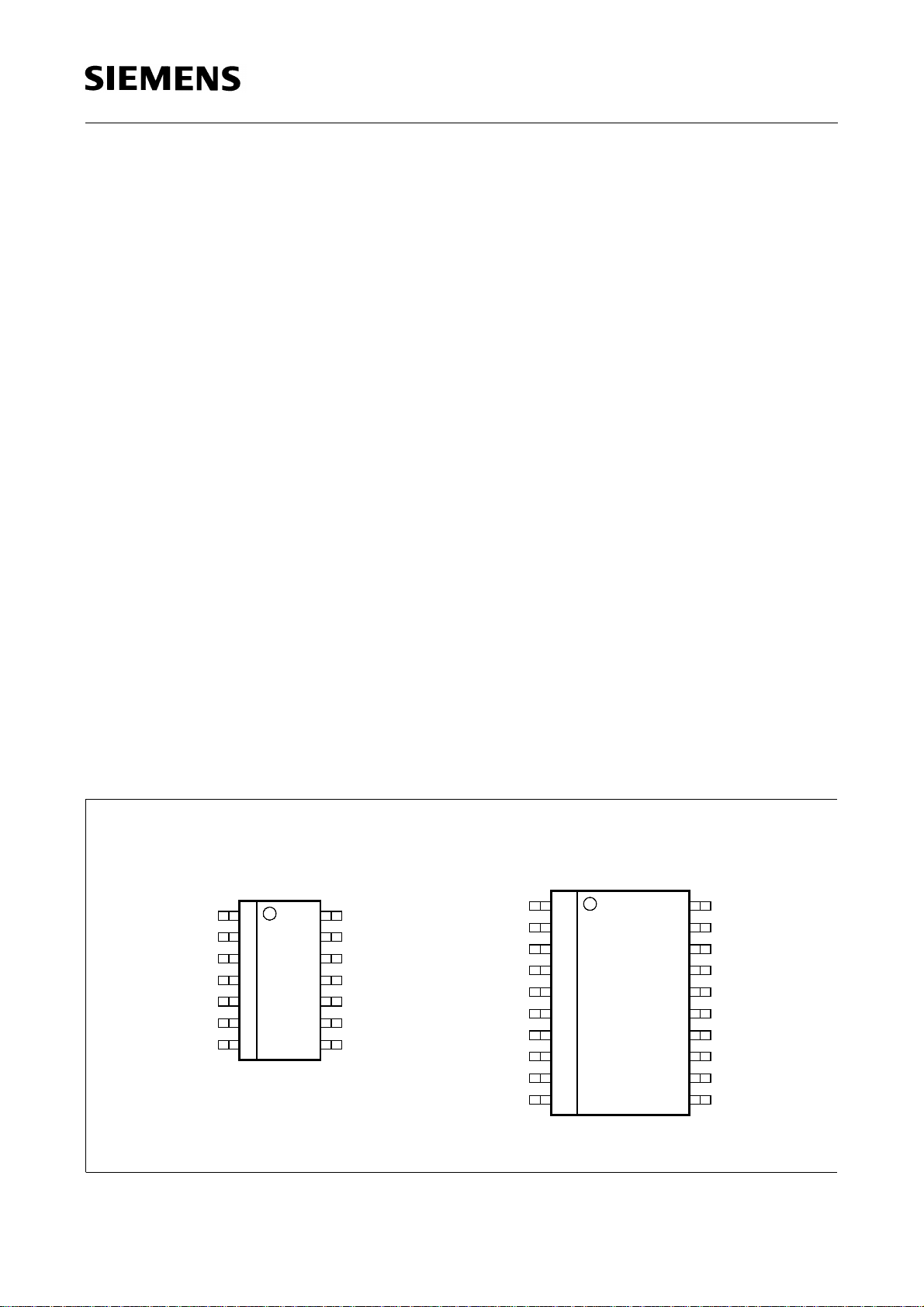
Pin Configuration
(top view)
P-DSO-20-6P-DSO-14-4
D
DIS
GND
GND
GND
RQ
SQ
114
2
3
4
5
6
7
13
12
10
11
9
8
AEP02152
SI
Ι
GND
GND
GND
Q2
Q1
RADJ
D
DIS
GND
GND
GND
GND
RQ
SQ
Q1
120
2
3
4
5
6
7
8
9
10
19
18
17
16
15
14
13
12
11
SI
Ι
1
2
Ι
GND
GND
GND
GND
Q2
Q2
ADJ2
AEP02151
Figure 1
Semiconductor Group 2 1998-11-01
TLE 4470
Pin Definitions and Functions
P-DSO-20-6
Pin No. Symbol Function
1RADJReset switching threshold adjust; for setting the reset
switching threshold connect to a voltage divider from Q1 to
GND. If this input is connected to GND, the reset is
triggered at the internal threshold.
C
2DReset delay; connect a capacitor
adjustment
3DISDisable input main regulator; Q2 disabled with high signal
4, 5, 6, 7 GND Ground
8RQReset output; the open collector output is connected to Q1
via an integrated 30 kΩ resistor
to GND for delay time
D
9SQSense output; the open collector output is connected to Q1
via an integrated 30 kΩ resistor
10 Q1 Stand-by regulator output voltage; block to GND w ith a
C
capacitor
≥ 6 µF, ESR < 10 Ω at 10 kHz
Q1
11 ADJ2 Main regulator adjust input; Q2 can be set to higher
values by an external divider
12, 13 Q2 Main regulator output voltage; block to GND with a
C
capacitor
≥ 10 µF, ESR < 10 Ω at 10 kHz
Q2
14, 15, 16, 17 GND Ground
18 I2 Main regulator input voltage; block to GND directly at the
IC with a ceramic capacitor
19 I1 Stand-by regulator input voltage; block to GND directly at
the IC with a ceramic capacitor
20 SI Sense comparator input
Semiconductor Group 3 1998-11-01
TLE 4470
P-DSO-14-4
Pin No. Symbol Function
C
1DReset delay; connect a capacitor
adjustment
2DISDisable input main regulator; Q2 disabled with high signal
3, 4, 5 GND Ground
6RQReset output; the open collector output is connected to Q1
via an integrated 30 kΩ resistor
7SQSense output; the open collector output is connected to Q1
via an integrated 30 kΩ resistor
8Q1Stand-by regulator output voltage; block to GND with a
C
capacitor,
≥ 6 µF, ESR < 10 Ω at 10 kHz
Q1
to GND for delay time
D
9Q2Main regulator output voltage; 5 V output tracking to Q1,
C
block to GND with a capacitor
≥ 10 µF, ESR < 10 Ω at
Q2
10 kHz
10, 11, 12 GND Ground
13 I Main and stand-by regulator input voltage; block to GND
directly at the IC with a ceramic capacitor
14 SI Sense comparator input
RADJ Reset switching threshold adjust not available in P-DSO-14-4 package. Reset
is always triggered at the internal threshold.
ADJ2 Main regulator adjust input is internally connected to
V
Q2
Semiconductor Group 4 1998-11-01
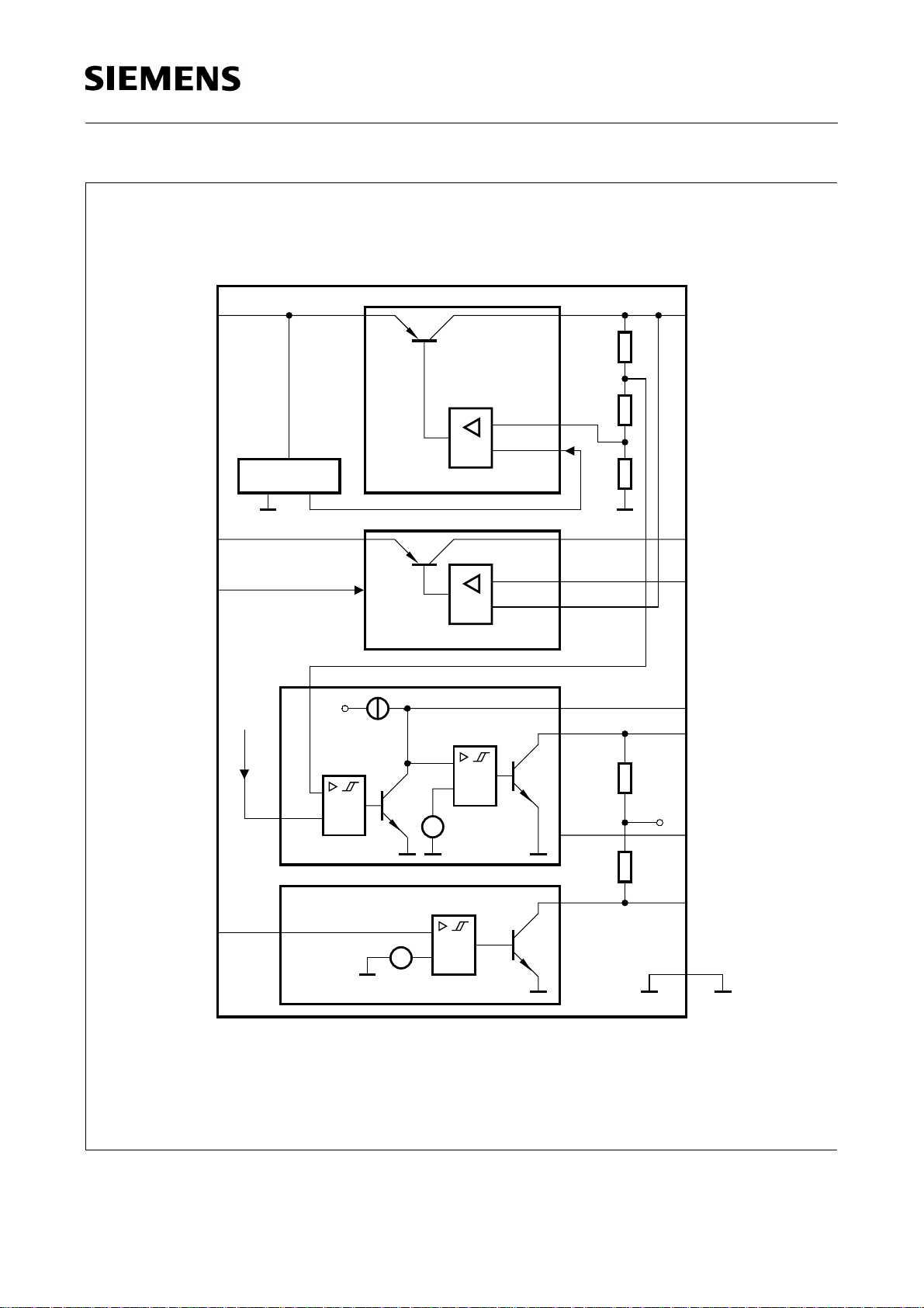
TLE 4470
Ι1
2Ι
DIS
19
18
3
V
REF
Reference
V
REF
Stand-by-Regulator
Main Regulator
Ι
d
10
12,
13
11
2
8
Q1
Q2
ADJ2
D
RQ
SI
Pin numbers valid for P-DSO-20-6 (TLE 4470 G)
Figure 2
Block Diagram
20
Reset
Sense
V
=
SITH
=
V
RADJTH
30 k
V
Q1
30 k
4-7
14-17
Ω
1
RADJ
Ω
9
SQ
GND
AEB02153
Semiconductor Group 5 1998-11-01
Absolute Maximum Ratings
– 40 °C < T
< 150 °C
j
Parameter Symbol Limit Values Unit Remarks
min. max.
V
Stand-by Regulator Input Voltage
I1
TLE 4470
Voltage
Current
Main Regulator Input Voltage
Voltage V
Current
Stand-by Output
V
Q1
Voltage
Current
Main Output
V
Q2
Voltage V
Current
V
I
I
V
I
I
V
I1
I1
I2
I2
I2
Q1
Q1
Q2
Q2
Main Regulator Adjust Input ADJ2
– 42 45 V –
– – mA Internally limited
– 42 45 V –
– – mA Internally limited
– 1 7 V –
– – mA Internally limited
– 1 36 V –
– – mA Internally limited
Voltage
Current
V
I
ADJ2
ADJ2
– 0.3 18 V –
– – mA Internally limited
Sense Output SQ
Voltage
Current
V
I
SQ
SQ
– 0.3 25 V –
– 5 5 mA –
Reset Output RQ
Voltage
Current
Semiconductor Group 6 1998-11-01
V
I
RQ
RQ
– 0.3 25 V –
– 5 5 mA –
Absolute Maximum Ratings (cont’d)
– 40 °C < T
< 150 °C
j
Parameter Symbol Limit Values Unit Remarks
min. max.
Disable Input DIS
TLE 4470
Voltage
Current
V
I
DIS
DIS
– 42 45 V –
– 2 2 mA –
Sense Input SI
Voltage
Current
V
I
SI
SI
– 25 18 V –
– 2 2 mA –
Reset Delay D
Voltage
Current
V
I
D
D
– 0.3 7 V –
– 2 2 mA –
Reset Switching Threshold Adjust RADJ
Voltage
Current
V
I
RADJ
RADJ
– 0.3 7 V –
– – mA Internally limited
Temperatures
Junction temperature
Storage temperature
T
j
T
stg
– 50 150 °C–
– 50 150 °C–
Note: ESD-Protection according to MIL Std. 883: ± 2 kV.
Maximum ratings are absol ute ratings; exceeding any one of thes e values may
cause irreversible damage to the integrated circuit.
Semiconductor Group 7 1998-11-01

TLE 4470
Operating Range
Parameter Symbol Limit Values Unit Remarks
min. max.
Stand-by regulator
input voltage
Main regulator
input voltage
Stand-by regulator
output current
Main regulator
output current
Disable input voltage
Sense input voltage
Junction temperature
Thermal Resistances
Junction pin
Junction ambient
V
V
I
I
V
V
T
R
R
I1
I2
Q1
Q2
DIS
SI
j
thj-pin
thj-a
5.6 45 V –
V
+
Qnom
45 V –
0.6 V
0 180 mA –
0 350 mA –
– 0.3 45 V –
– 0.3 17 V –
– 40 150 °C–
– 25 K/W Measured to pin 4
–65K/W–
Note: In the operating range the functions given in the circuit description are fulfilled.
Semiconductor Group 8 1998-11-01

TLE 4470
Electrical Characteristics
V
= V
I1
= 14 V; V
I2
Parameter Symbol Limit Values Unit Test Condition
Stand-by Regulator
Output 1
DIS
< V
; – 40 °C < Tj < 150 °C; unless otherwise specified
DISL
min. typ. max.
Output voltage
Output current
V
I
limitation
Output drop voltage;
V
DRQ1
= V
I1
– V
Q1
V
Current Consumption
Quiescent current;
I
stand-by
I
= II1 – I
q
Quiescent current
I
= II1 – I
q
Q1
I
Q1
Regulator Performance
Load regulation ∆
Q1
Q1
DRQ1
q
q
V
Q1
4.90 5.0 5.10 V 1 mA < IQ1<100mA
180 280 – mA see note 1
– 300 500 mV IQ1 = 100 mA; s ee note 1
– 180 250 µA IQ1 = 300 µA; Tj = 25 °C
V
> V
DIS
DISH
– 180 300 µA IQ1 = 300 µA;
V
> V
DIS
DISH
–46mAIQ1 = 100 mA
–15 50mV1mA<IQ1<150mA;
Load regulation ∆
Line regulation ∆
Power-Supply-Ripple-
PSRR
Rejection
Temperature output
∆V
V
V
Q1
Q1
Q1
–5 25mV1mA<IQ1<100mA;
–5 20mVI
= 1 mA;
Q1
6V<
V
I1
<28V
–60 –dB20Hz<fr<20kHz;
V
= 5 V
r
/∆T – 0.3 – mV/K –
SS
voltage drift
V
/dt stability V
d
I1
Value of output
C
Q1
Q1
4.5 – 5.5 V no reset occurs; note 3
6– –µF–
capacitance
ESR of output
R
ESRQ1
–– 10Ω at 10 kHz
capacitance
Semiconductor Group 9 1998-11-01

TLE 4470
Electrical Characteristics (cont’d)
V
= V
I1
= 14 V; V
I2
Parameter Symbol Limit Values Unit Test Condition
Main-Regulator
Output 2
Output voltage
tracking accuracy
Output voltage
tracking accuracy
DIS
< V
; – 40 °C < Tj < 150 °C; unless otherwise specified
DISL
min. typ. max.
V
– VQ1– 25 5 25 mV 5 mA < IQ2< 100 mA;
Q2
V
V
I2
I2
<40V
<28V
6V<
V
– VQ1– 25 5 25 mV 5 mA < IQ2< 250 mA;
Q2
7V<
see note 2
Adjust input current
Output current
I
I
limitation
Output drop voltage
V
DRQ2
= V
I2
– V
Q2
V
Current Consumption
Quiescent current;
I
= II – I
q
Q
Quiescent current;
I
= II – I
q
Q
I
I
Regulator Performance
Load regulation ∆
Line regulation ∆
ADJ2
Q2
DRQ2
q
q
V
V
Q2
Q2
– 1 – 1 µA–
350 500 – mA see note 1
– 300 600 mV IQ2 = 200 mA; see note 1
–715mAIQ2 = 200 mA
I
= 300 µA
Q1
– 250 500 µA IQ2 = IQ1 = 300 µA;
= 25 °C
T
j
–5 25mV5mA<IQ2< 200 mA;
–5 20mVIQ2 = 5 mA;
6V<V
<28V
I2
Power-Supply-RippleRejection
Temperature output
PSRR
V
∆
Q2
–60 –dB20Hz<fr<20kHz;
V
= 5 Vss
r
/∆T – 0.5 – mV/K –
voltage drift
V
/dt stability V
d
I2
Value of output
C
Q2
Q2
4.5 – 5.5 V no reset occurs; note 2
10 – – µF–
capacitance
Semiconductor Group 10 1998-11-01

TLE 4470
Electrical Characteristics (cont’d)
V
= V
I1
= 14 V; V
I2
Parameter Symbol Limit Values Unit Test Condition
DIS
< V
; – 40 °C < Tj < 150 °C; unless otherwise specified
DISL
min. typ. max.
ESR of output
R
ESRQ2
capacitance
Disable Input DIS
H-input voltage
V
DISH
threshold
L-input voltage
V
DISL
threshold
H-input current
L-input current
I
DISH
I
DISL
Reset Timing D and Output RQ
Reset switching
V
RT
threshold
Reset adjust
V
RADJTH
threshold
–– 10Ω at 10 kHz
1.8 2.0 2.3 V –
1.4 1.7 2.0 V Output 2 active
–2 – 1 1 µA 2.3V<V
–6 –2 – 0.5 µA 0V<V
DIS
<1.4V
DIS
<7V
4.5 4.65 4.8 V RADJ connected to GND
1.25 1.35 1.45 V VQ1 > 3.5 V
Reset output low
voltage
Reset hi gh voltage
Reset pull up resistor
Reset charging
current
Upper timing
threshold
Lower timing
threshold
Reset delay time
Reset reaction time
V
V
R
I
V
V
t
t
d
d
RR
RQL
RQH
RQ
DU
DL
– 0.15 0.3 V RRQ = 10 kΩ external
connected to
V
≥ 1V
Q1
V
Q1;
4.5 – – V –
20 30 45 kΩ Internal connected to V
359µA VD = 1 V
1.5 1.8 2.2 V –
0.3 0.4 0.55 V –
12 15 20 ms CD = 47 nF
–0.52.0µs CD = 47 nF
Q1
Semiconductor Group 11 1998-11-01

TLE 4470
Electrical Characteristics (cont’d)
V
= V
I1
= 14 V; V
I2
Parameter Symbol Limit Values Unit Test Condition
Sense Input SI and Output SQ
DIS
< V
; – 40 °C < Tj < 150 °C; unless otherwise specified
DISL
min. typ. max.
Sense threshold
V
SITH
1.28 1.35 1.45 V VSI decreasin g
voltage
Sense threshold
V
SIHY
25 60 100 mV –
hysteresis
Sense output low
V
SQL
– 0.15 0.4 V RSQ = 10 kΩ external
voltage
Sense output high
V
SQH
4.5 – – V VSI>1.5V
voltage
Sense pull up resistor
R
SQ
20 30 45 kΩ Internal connected to V
Note 1: Measured when the output voltage
value.
V
Note 2:
Note 3: Square wave at
connected to ADJ2
Q2
V
I
: 8 V to 18 V;
f
= 10 kHz;
connected to
V
= 1.1 V; VI1> 4.5 V
SI
V
has dropped 100 mV from the nominal
Q
t
=
t
≤
r
100 ns
f
V
Q1
Q1
Semiconductor Group 12 1998-11-01

Application Information
D1
1N4004
V
Batt
ZD1
C
Ι
36 V 100
nF
19
1
Ι
18
Ι
2
Reference
V
REF
Stand-by-Regulator
10
12,
13
Q1
Q2
( = )
TLE 4470
5 V
C
Q1
10 F
µ
R
R
1
2
10 V
C
Q2
µ
22 F
Control
R
SI1
DIS
3
Main Regulator
330 kΩ
V
REF
Ι
d
Reset
SI
20
V
=
SITH
R
SI2
100 kΩ
C
SI
10 nF
Sense
Pin numbers valid for P-DSO-20-6 (TLE 4470 G)
=
V
RADJTH
11
30 k
Ω
V
Q1
30 kΩ
4-7
14-17
2
8
1
9
ADJ2
100 nF
D
RQ
RADJ
SQ
GND
R
1
R
2
C
D
AES02154
Figure 3
Application Circuit
Semiconductor Group 13 1998-11-01

TLE 4470
Input, Output
C
The inpu t c a pa c ito r
approx. 1 Ω in series with
be damped. To stabilize the regulation circuits of the stand-by and main regulator, output
C
capacitors
C
≥ 10 µF, both with an ESR ≤ 10 Ω within the operating temperature range.
Q2
and CQ2 are necessary. Stabi lity is guaranteed at values CQ1≥ 6 µF &
Q1
For the TLE 4470 G (P-DSO-20-6) the output voltage
adjusted to 5 V ≤
adjust pin VA. For
main output.
For calculating
V
is necessary for compensating line influences. Using a resistor of
I
C
, the LC circuit of input inductivity and input capacitance can
I
V
of the main regulator c an be
Q2
V
Q
Q2rated
V
or R
≤ 20 V by connecting an external voltage divider to the voltage
= 5 V the voltage adjust pin has to be co nnected directly to the
Q2
& R2 respectively the following equations can be used:
1
V
= V
Q
× (R1 + R2) / R
ref
2
or
R
= R × (VQ / V
1
R
= R × R1 / (R1 – R)
2
ref
)
Definitions:
R = R
V
ref
// R2 ; R ≈ 100 kΩ
1
= Output voltage of stand by regulator, typical 5 V
Disable
The main regulator of the TLE 4470 can be switched OFF by a volt age of 2.3 V at pin
DIS. Reducing this voltage below 1.4 V will switch ON the main regulator again.
Reset Timing
The power-on reset delay time is defi ned by the charging time of an external capacito r
C
which can be calculated as follows:
d
C
= (∆td × Id) / ∆V
d
C
Definitions:
The reset reaction time
= delay capacitor
d
t
= delay time
∆
d
I
= charge current, typical 5 µA
d
V
∆V=
V
dt
, typical 1.8 V
dt
= upper delay switching threshold at Cd for reset delay time
t
is the time it takes the voltage regulator to set the reset out
rr
LOW after the output voltage has drop ped bel ow the res et thresh old. It i s typic ally 2 µs
C
for delay capacitor of 100 nF. For other values for
the reaction time can be estimated
d
using the following equation:
t
≈ 20 s/F × C
rr
Semiconductor Group 14 1998-11-01
d

TLE 4470
V
Ι
t
<
RR
V
RT
V
Q
Ι
V
d
d
=
dt
C
D
V
D
t
d
t
RR
V
DT
V
ST
V
RO
Power-on-Reset Voltage Dip Secondary Overload
Thermal
Shutdown
at Input
Undervoltage
at OutputSpike
AED01542
Figure 4
Reset Timing
Reset Switching Threshold
The internally set rese t threshold is 4.65 V. When u sin g the TLE 447 0 G (P-DSO-20-6)
V
this threshold can be adjusted to 3.5 V <
< 4.6 V by connecting an external voltage
RTH
divider to pin RADJ. If this pin is not needed, it can be left open or even better connected
to GND.
R
Definitions: V
V
= R2 × (VRT – V
1
= Reset threshold
RT
= comparator reference voltage, typical 1.35 V
ref
ref
) / V
ref
(Reset adjust input current ≈ 50 nA)
The reset output pin is internally connected to the stand-by output Q1 via a 30 kΩ pull-up
V
resistor. The reset LOW signal at pin RQ in guaranteed down to an output voltage
Q1
of
1 V typical.
Semiconductor Group 15 1998-11-01

TLE 4470
V
V
I1
30 k
Ω
Q1
GND
RO
RADJ
R
1
R
2
AES02505
Band-Gap
Reference
1.35 V 1.35 V
TLE 4470 G
Band-Gap
Reference
_
<
1
+
_
Figure 5
Early Warning
The early warning function compares a voltage defined by the user to an internal
reference voltage. Therefore the voltage to be supervise d ha s to be s ca led down by an
external voltage divider in order to compare it to internal sense threshold (reference
voltage) which is typically 1.35 V. The sense out pin is set to low when the user defined
voltage falls below this threshold.
V
A typical example where this circuit can be used is to supervise the input vo ltage
to
I
give the microprocessor a prewarning of a low battery condition.
Calculation of the voltage di vider can be easily don e since the sense input curre nt can
be neglected.
R
To minimize transient influences the use of a capacitor in parallel to
is recommended.
2
Like the reset output pin, the sense out pin SQ is internall y connected to the stan d-by
output Q1 via a 30 kΩ pull-up resistor. The sense out LOW signal at pin SQ is generated
V
down to an input voltage
Semiconductor Group 16 1998-11-01
of 3 V typical.
I1

Typical Performance
j
Characteristics
V
Drop Voltage
600
mV
500
I
Q1
=
V
V
dr
V
OFF
Q2
Current
V
dr
versus Output 1
dr
-0.1 V
Qnom
AED02491
TLE 4470
Output Voltage VQ1/VQ2 versus Output
Current
V
/
Q1
I
Q1
6
V
Q2
V
T
j
= 25 ˚C
AED02493
5
400
300
T
= 125 ˚C
j
T
= 25 ˚C
200
j
T
= -40 ˚C
j
100
0
0
50 100 150 200
mA
Ι
300
Q1
Drop Voltage Vdr versus Output 2
600
mV
500
I
Q2
AED02492
=
V
V
Qnom
-0.1 V
dr
Current
V
dr
4
V
Q1
3
2
1
0
0
100 200 300 400 500
Output 1 Voltage VQ1 versus
T
Temperature
5.2
V
Q1
V
5.1
j
V
Q2
mA
Ι
Q1
AED02494
V
= 13.5 V
Ι
4.9
4.8
4.7
4.6
5
-40
0 40 80 120 160
˚C
T
400
300
200
100
0
0
50 100 150 200
T
= 125 ˚C
j
T
= 25 ˚C
j
T
= -40 ˚C
j
mA
Ι
300
Q2
Semiconductor Group 17 1998-11-01

TLE 4470
Output Voltage VQ1, VQ2 versus Input
V
1
0
(VI1 = VI2)
I
=
V
V
Ι
Q
T
= 25 ˚C
j
Ι
= 10 mA
Q1
Ι
= 10 mA
Q2
V
Q1nom
24
AED02495
V/V
Q1
Q2
=
V
= 5 V
Q2nom
6810
V
V
Ι
Voltage
6
V
Q
V
5
4
3
2
0
Current Consumption
I
Output 1 Current
Ι
3000
q
2500
2000
1500
1000
µ
500
T
= 25 ˚C
A
j
V
= 13.5 V
Ι
V
OFF
Q2
0
0
10 20 30 40
(low load)
Q1
I
versus
q
AED02497
mA
Ι
Q1
Current Consumption
V
Voltage
Ι
q
mA
I
6
T
= 25 ˚C
j
Ι
< 1 mA
Q1
Ι
= 10 mA
Q2
5
4
3
2
1
0
0
10 20 30 40
I
versus Input
q
AED02496
V
V
Ι
Current Consumption
I
Output 1 Current
30
Ι
q
mA
25
20
15
10
5
0
T
= 25 ˚C
j
V
= 13.5 V
Ι
V
OFF
Q2
0
50 100 150 200 250
(high load)
Q1
I
versus
q
AED02498
mA
Ι
Q1
Semiconductor Group 18 1998-11-01

TLE 4470
Current Consumption Iq versus
I
Output 2 Current
Ι
1800
q
1500
1200
µ
900
600
300
T
= 25 ˚C
A
0
j
V
= 13.5 V
Ι
Ι
= 0 mA
Q1
0
10 20 30 40 60
(low load)
Q2
AED02499
mA
Ι
Q2
Reset Adjust Threshold
T
Temperature
1.6
V
RADJTH
V
1.5
1.4
1.3
1.2
1.1
1.0
-40
j
0 40 80 120 160
V
RADJTH
versus
AED02501
˚C
T
j
Current Consumption
I
Output 2 Current
30
Ι
mA
q
25
20
15
10
5
0
0
50 100 150 200
(high load)
Q2
I
versus
q
AED02500
300
mA
Ι
Q2
Switching Voltage
T
Temperature
2,4
V
V
D
2.0
1.6
1.2
0.8
0.4
0
-40
j
= 13,5 V
V
Ι
V
DU
0 40 80 120 160
V
, VDL versus
DU
AED02502
˚C
T
j
Semiconductor Group 19 1998-11-01

TLE 4470
Charge Current Id versus
T
Temperature
8
Ι
d
V
A
µ
7
6
5
4
3
2
-40
Ι
V
D
j
= 13.5 V
= 1 V
0 40 80 120 160
AED02503
˚C
T
j
Sense Threshold
T
Temperature
1.6
V
SITH
V
1.5
1.4
1.3
1.2
1.1
1
-40
j
V
= 13.5 V
Ι
0 40 80 120 160
V
SITH
versus
AED02504
T
˚C
j
Semiconductor Group 20 1998-11-01

Package Outlines
P-DSO-14-4
(Plastic Dual Small Outline)
-0.1
0.2
-0.2
1.45
4
-0.2
1.75 max
TLE 4470
0.35 x 45˚
1)
+0.06
0.19
0.35
1.27
+0.15
2)
0.1
0.2 14x
±0.2
6
0.4
+0.8
8˚ max.
14 8
17
8.75
-0.2
1)
Index Marking
1) Does not include plastic or metal protrusion of 0.15 max. per side
2) Does not include dambar protrusion of 0.05 max. per side
GPS05093
Sorts of Packing
Package outlines for tubes, trays etc. are contained in our
Data Book “Package Information”.
SMD = Surface Mounted Device
Dimensions in mm
Semiconductor Group 21 1998-11-01

P-DSO-20-6
(Plastic Dual Small Outline)
1.27
+0.15
0.35
2)
0.2 24x
1120
-0.1
0.2
-0.2
2.45
0.1
7.6
2.65 max
10.3
0.35 x 45˚
1)
-0.2
+0.8
0.4
±0.3
+0.09
0.23
TLE 4470
8˚ max
GPS05094
110
12.8
-0.2
1)
Index Marking
1) Does not include plastic or metal protrusions of 0.15 max per side
2) Does not include dambar protrusion of 0.05 max per side
Sorts of Packing
Package outlines for tubes, trays etc. are contained in our
Data Book “Package Information”.
SMD = Surface Mounted Device
Dimensions in mm
Semiconductor Group 22 1998-11-01
 Loading...