Siemens TLE4470GS, TLE4470G Datasheet
Dual Low-Drop Voltage Regulator TLE 4470
Features
• Stand-by output 180 mA; 5 V ± 2%
• Adjustable reset switching threshold
• Main output 350 mA; tracked to the stand-by output
• Low quiescent current consumption in standby mode
• Disable function for main output
• Wide operation range: up to 45 V
• Very low dropout
• Power-On-Reset circuit sensing the stand-by voltage
• Early warning comparator for supply undervoltage
• Output protected against short circuit
• Wide temperature range: – 40 °C to 150 °C
• Over-temperature protection
• Over-load protection
P-DSO-14-4
P-DSO-20-6
Type Ordering Code Package
TLE 4470 GS Q67006-A9309 P-DSO-14-4 (SMD)
TLE 4470 G Q67006-A9308 P-DSO-20-6 (SMD)
Functional Description
The TLE 4470 is a monolithic integrated voltage regulator with two very low-drop
outputs, a main output Q2 for loads up to 350 mA and a stand by output Q1 providing a
maximum of 180 m A. T he device is availa ble i n both the P-DSO-14-4 and P-DSO - 20-6
packages. It is designed to supply microprocessor systems under the severe conditions
of automotive applications and is therefore equipped with additional protection functions
against over load, short circuit and over t emperatu re. Of course the TLE 4470 can also
be used in other applications where two stabilized voltages are required.
The device operates in the wide temperature range of – 40 °C to 150 °C.
V
The stand by regulator transforms an input voltage
V
Q1rated
= 5 V within an accura cy of 2%, whereas the main r egulato r is adj ustable . By use
of an external voltage divider the main output voltage can be s et to
Semiconductor Group 1 1998-11-01
in the range of 5.6 V ≤ VI≤ 45 V to
I
V
≥ 5 V for the
Q2
TLE 4470
TLE 4470 G type (P-DSO-20-6 package). VQ1 is compared to the voltage at pin VA,
V
which is proportional to the output voltage
series PNP transistor via a buffer.
V
The main output voltage
is tracked to the accuracy of the stand by output.
Q2
For the TLE 4470 GS (P-DSO-14-4 package) the output voltage is fixed to 5 V.
To save energy e.g. in battery powered body electronic applications, the main regulator
can be switched off via the disable input, which causes the current consumption to drop
to 180 µA typical.
Two additional features of the TLE 4470 are an early warning comparator (can be used
V
e.g. to monitor the supply voltage
) and reset generator with an adjustable reset delay
I
time. The TLE 4470 G (P-DSO-20-6 package) has in addition an adjustable reset
switching threshold. This feature is useful with microprocessors which guarantee a safe
operation down to voltages below the internally set reset threshold of 4.65 V typical.
. A control amplifier drives the base of the
Q2
Two functions are included in the reset generator, a power on reset and an under-voltage
reset. The power on reset feature is necessary for a defined start of the microprocessor
when switching on the application. The reset LOW
V
time after the output vol tage
of the regulator has surpassed th e reset thresh old. An
Q1
signal is generated for a certain delay
external delay capacitor s ets th e delay time. T he unde r vol tage res et circu it sup ervises
V
the stand-by output voltage. In case
falls below the reset switchin g threshold the
Q1
reset output is set LOW after a sh ort reaction tim e. The reset LOW si gnal is gene rated
V
down to an output voltage
of 1 V.
Q1
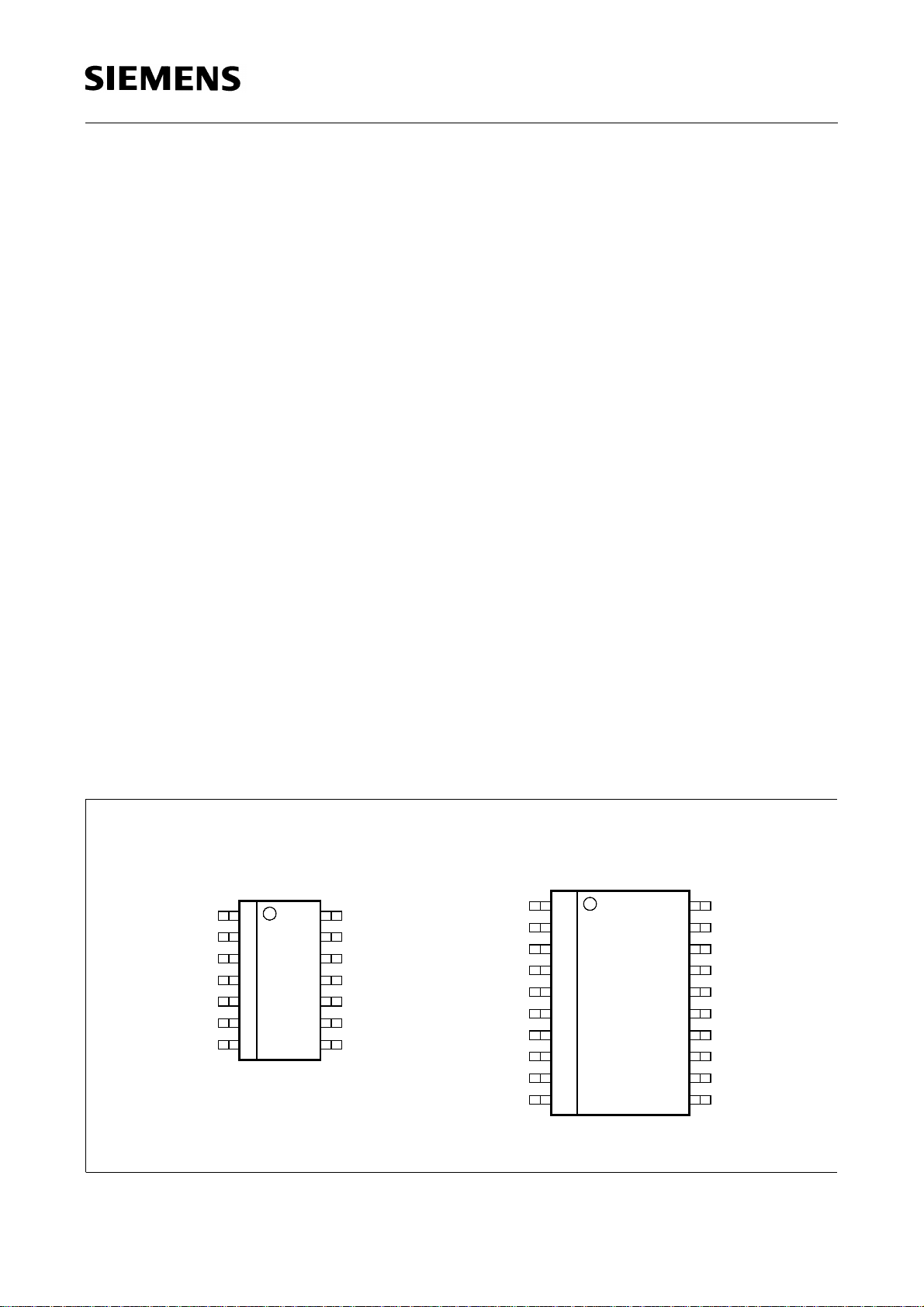
Pin Configuration
(top view)
P-DSO-20-6P-DSO-14-4
D
DIS
GND
GND
GND
RQ
SQ
114
2
3
4
5
6
7
13
12
10
11
9
8
AEP02152
SI
Ι
GND
GND
GND
Q2
Q1
RADJ
D
DIS
GND
GND
GND
GND
RQ
SQ
Q1
120
2
3
4
5
6
7
8
9
10
19
18
17
16
15
14
13
12
11
SI
Ι
1
2
Ι
GND
GND
GND
GND
Q2
Q2
ADJ2
AEP02151
Figure 1
Semiconductor Group 2 1998-11-01
TLE 4470
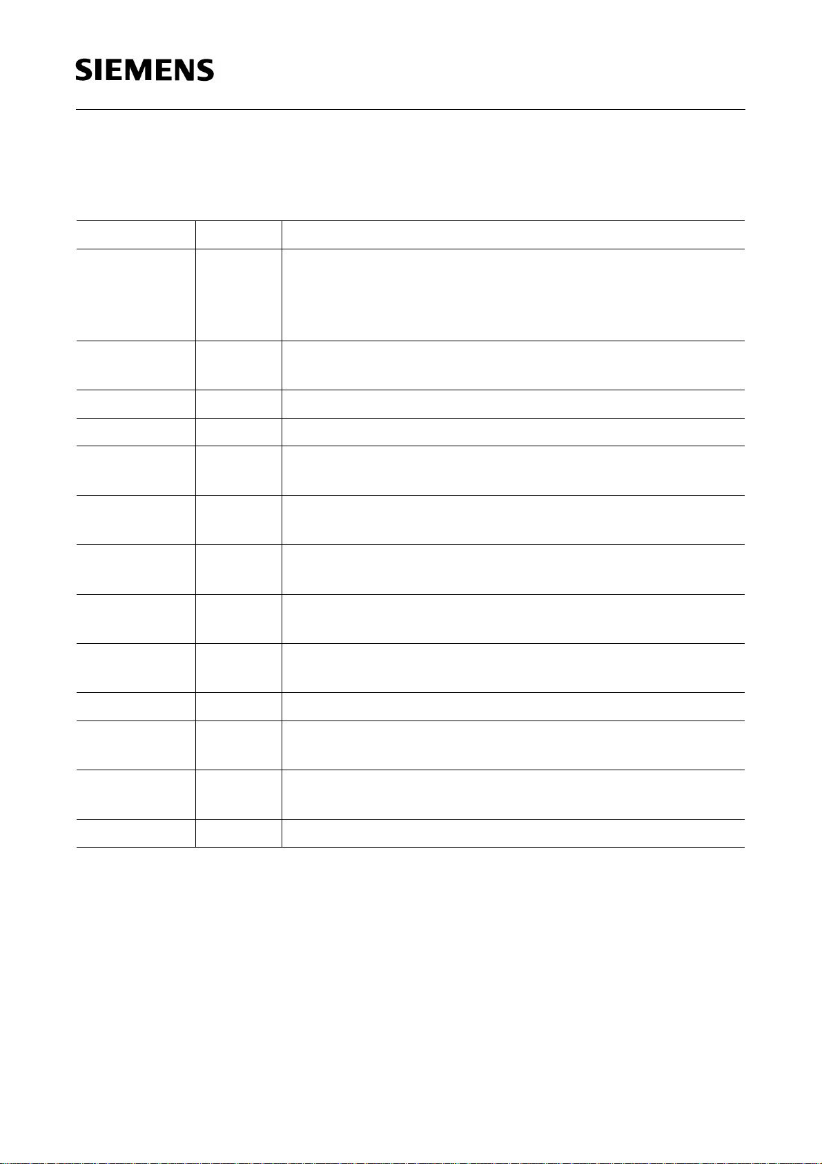
Pin Definitions and Functions
P-DSO-20-6
Pin No. Symbol Function
1RADJReset switching threshold adjust; for setting the reset
switching threshold connect to a voltage divider from Q1 to
GND. If this input is connected to GND, the reset is
triggered at the internal threshold.
C
2DReset delay; connect a capacitor
adjustment
3DISDisable input main regulator; Q2 disabled with high signal
4, 5, 6, 7 GND Ground
8RQReset output; the open collector output is connected to Q1
via an integrated 30 kΩ resistor
to GND for delay time
D
9SQSense output; the open collector output is connected to Q1
via an integrated 30 kΩ resistor
10 Q1 Stand-by regulator output voltage; block to GND w ith a
C
capacitor
≥ 6 µF, ESR < 10 Ω at 10 kHz
Q1
11 ADJ2 Main regulator adjust input; Q2 can be set to higher
values by an external divider
12, 13 Q2 Main regulator output voltage; block to GND with a
C
capacitor
≥ 10 µF, ESR < 10 Ω at 10 kHz
Q2
14, 15, 16, 17 GND Ground
18 I2 Main regulator input voltage; block to GND directly at the
IC with a ceramic capacitor
19 I1 Stand-by regulator input voltage; block to GND directly at
the IC with a ceramic capacitor
20 SI Sense comparator input
Semiconductor Group 3 1998-11-01
TLE 4470
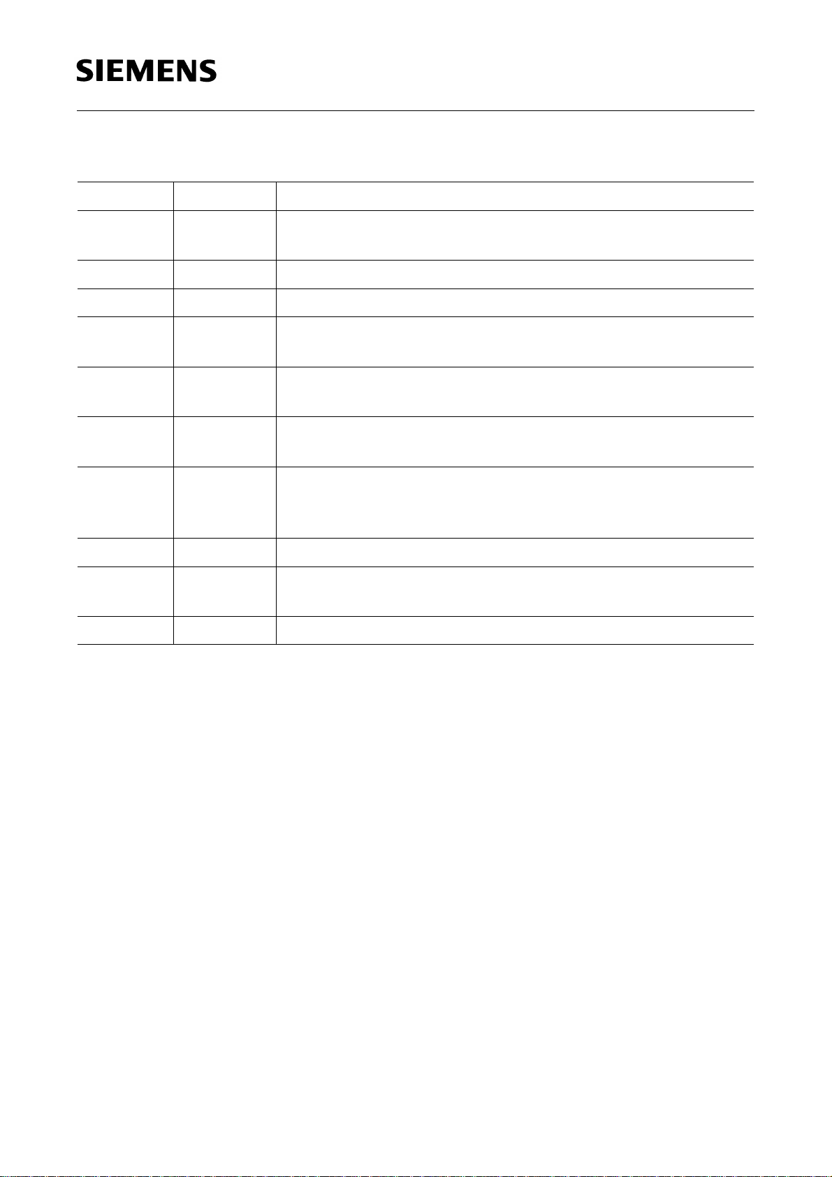
P-DSO-14-4
Pin No. Symbol Function
C
1DReset delay; connect a capacitor
adjustment
2DISDisable input main regulator; Q2 disabled with high signal
3, 4, 5 GND Ground
6RQReset output; the open collector output is connected to Q1
via an integrated 30 kΩ resistor
7SQSense output; the open collector output is connected to Q1
via an integrated 30 kΩ resistor
8Q1Stand-by regulator output voltage; block to GND with a
C
capacitor,
≥ 6 µF, ESR < 10 Ω at 10 kHz
Q1
to GND for delay time
D
9Q2Main regulator output voltage; 5 V output tracking to Q1,
C
block to GND with a capacitor
≥ 10 µF, ESR < 10 Ω at
Q2
10 kHz
10, 11, 12 GND Ground
13 I Main and stand-by regulator input voltage; block to GND
directly at the IC with a ceramic capacitor
14 SI Sense comparator input
RADJ Reset switching threshold adjust not available in P-DSO-14-4 package. Reset
is always triggered at the internal threshold.
ADJ2 Main regulator adjust input is internally connected to
V
Q2
Semiconductor Group 4 1998-11-01
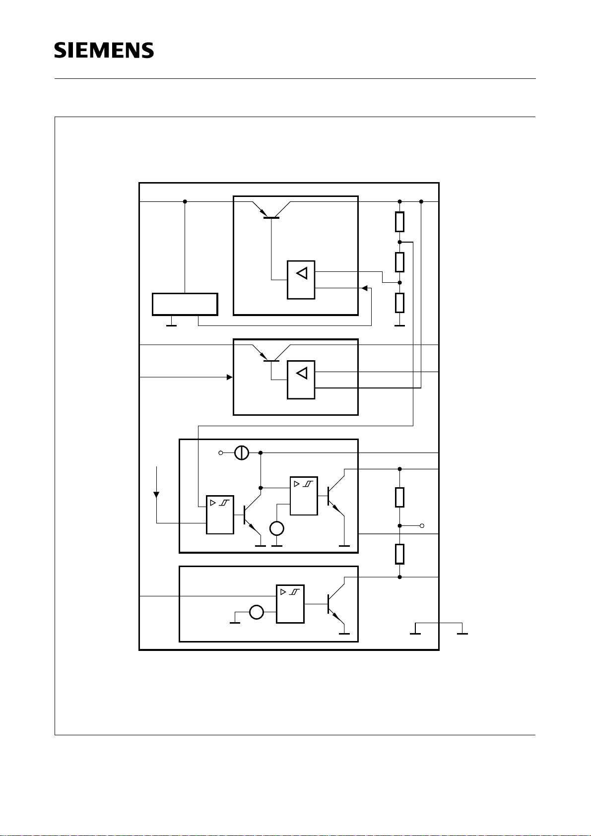
TLE 4470
Ι1
2Ι
DIS
19
18
3
V
REF
Reference
V
REF
Stand-by-Regulator
Main Regulator
Ι
d
10
12,
13
11
2
8
Q1
Q2
ADJ2
D
RQ
SI
Pin numbers valid for P-DSO-20-6 (TLE 4470 G)
Figure 2
Block Diagram
20
Reset
Sense
V
=
SITH
=
V
RADJTH
30 k
V
Q1
30 k
4-7
14-17
Ω
1
RADJ
Ω
9
SQ
GND
AEB02153
Semiconductor Group 5 1998-11-01
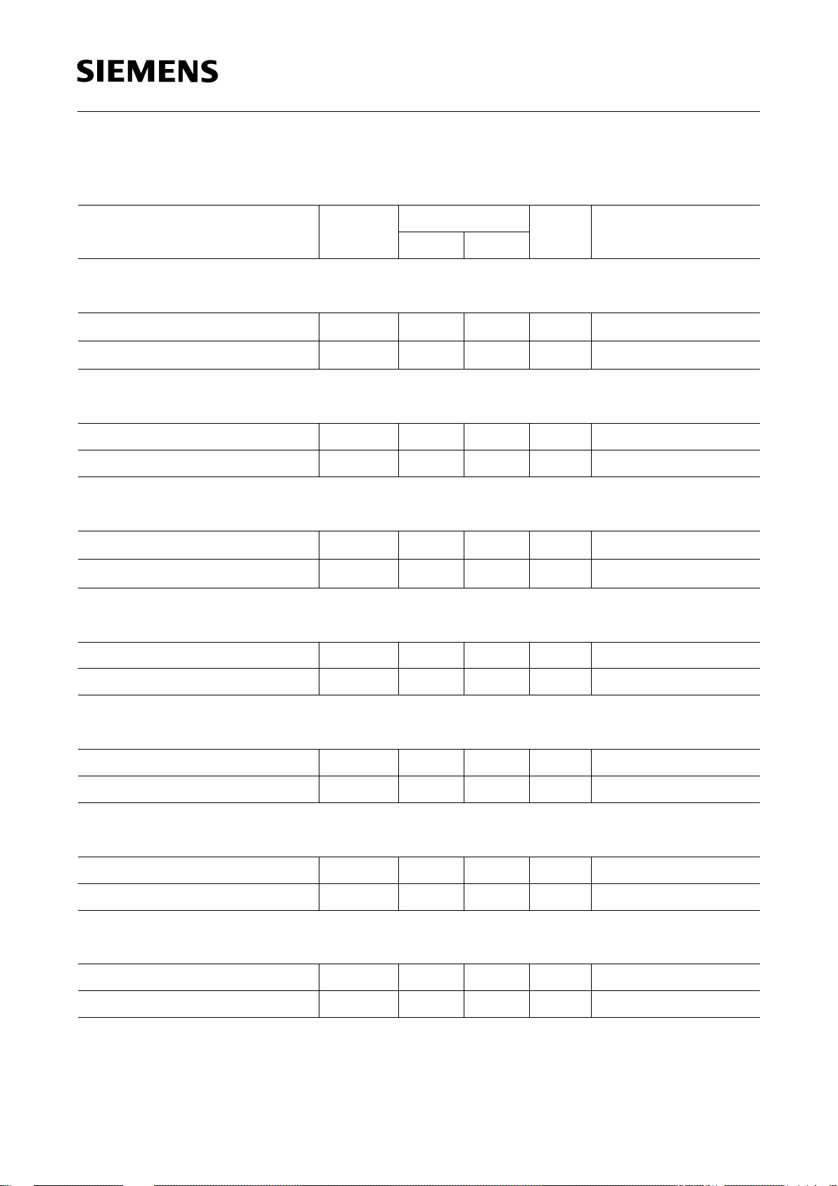
Absolute Maximum Ratings
– 40 °C < T
< 150 °C
j
Parameter Symbol Limit Values Unit Remarks
min. max.
V
Stand-by Regulator Input Voltage
I1
TLE 4470
Voltage
Current
Main Regulator Input Voltage
Voltage V
Current
Stand-by Output
V
Q1
Voltage
Current
Main Output
V
Q2
Voltage V
Current
V
I
I
V
I
I
V
I1
I1
I2
I2
I2
Q1
Q1
Q2
Q2
Main Regulator Adjust Input ADJ2
– 42 45 V –
– – mA Internally limited
– 42 45 V –
– – mA Internally limited
– 1 7 V –
– – mA Internally limited
– 1 36 V –
– – mA Internally limited
Voltage
Current
V
I
ADJ2
ADJ2
– 0.3 18 V –
– – mA Internally limited
Sense Output SQ
Voltage
Current
V
I
SQ
SQ
– 0.3 25 V –
– 5 5 mA –
Reset Output RQ
Voltage
Current
Semiconductor Group 6 1998-11-01
V
I
RQ
RQ
– 0.3 25 V –
– 5 5 mA –
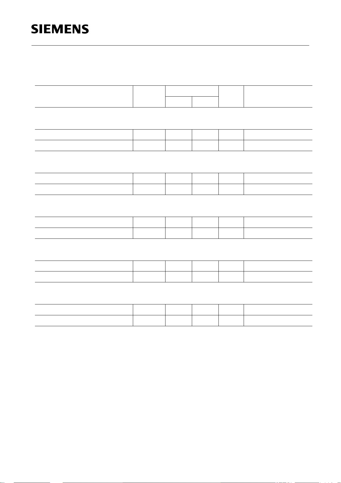
Absolute Maximum Ratings (cont’d)
– 40 °C < T
< 150 °C
j
Parameter Symbol Limit Values Unit Remarks
min. max.
Disable Input DIS
TLE 4470
Voltage
Current
V
I
DIS
DIS
– 42 45 V –
– 2 2 mA –
Sense Input SI
Voltage
Current
V
I
SI
SI
– 25 18 V –
– 2 2 mA –
Reset Delay D
Voltage
Current
V
I
D
D
– 0.3 7 V –
– 2 2 mA –
Reset Switching Threshold Adjust RADJ
Voltage
Current
V
I
RADJ
RADJ
– 0.3 7 V –
– – mA Internally limited
Temperatures
Junction temperature
Storage temperature
T
j
T
stg
– 50 150 °C–
– 50 150 °C–
Note: ESD-Protection according to MIL Std. 883: ± 2 kV.
Maximum ratings are absol ute ratings; exceeding any one of thes e values may
cause irreversible damage to the integrated circuit.
Semiconductor Group 7 1998-11-01
 Loading...