Siemens TLE4269GM, TLE4269GL, TLE4269G, TLE4269A Datasheet

TLE 4269
5-V Low-Drop Fixed Voltage Regulator
Features
● Output voltage tolerance ≤ ± 2 %
● Very low current consumption
● Early warning
● Reset output low doown to V
● Overtemperature protection
● Reverse polarity proof
● Settable reset threshold
● Very low drop voltage
● Wide temperature range
● Integrated pull up resistor at logic outputs
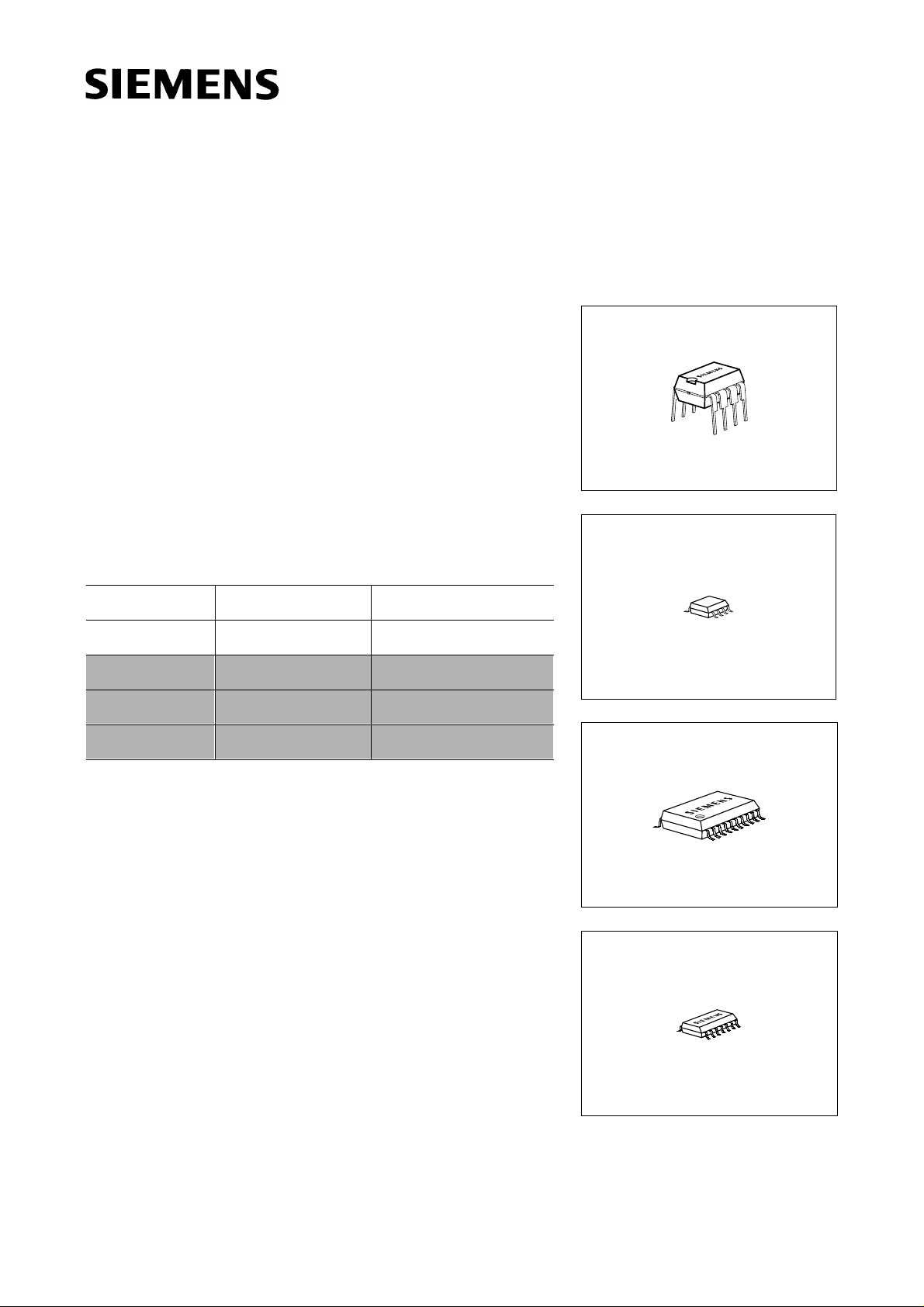
Type Ordering Code Package
= 1 V
Q
TLE 4269
P-DIP-8-4
TLE 4269 A Q67000-A9190 P-DIP-8-4
TLE 4269 G Q67006-A9173 P-DSO-8-1 (SMD)
TLE 4269 GM Q67006-A9288 P-DSO-14-4 (SMD)
▼
TLE 4269 GL Q67006-A9192 P-DSO-20-6 (SMD)
▼ New type
Functional Description
This device is a voltage regulator with a fixed 5-V
output, e.g. in a P-DSO-8-1 package. The maximum
operating voltage is 45 V. The output is able to drive a
150 mA load. It is short circuit protected and the
thermal shutdown switches the output off if the junction
temperature is in excess of 150 °C. A reset signal is
V
generated for an output voltage of
<4.6V. The
Q
reset threshold voltage can be decreased by external
connection of a voltage divider. The reset delay time
can be set by an external capacitor. R eset and sense
output have integrated pull up resistors. If the
integrated resistors are not desired TLE 4279 can be
used. It is also possi ble to supervise the input voltage
by using an integrated comparator to give a low voltage
warning.
P-DSO-8-1
P-DSO-20-6
P-DSO-14-4
Semiconductor Group 1 1998-11-01

Pin Configuration
(top view)
TLE 4269
P-DIP-8-4
P-DSO-8-1
18
Ι Q
S
RE
Ι
AEP01813
SO72
R63
GNDD54
Ι
2
ΙS
RE
3
D5
4
8
7
6
AEP01668
Q
SO
R
GND
1
Pin Definitions and Functions (TLE 4269 A and TLE 4269 G)
Pin No. Symbol Function
1 I Input; block directly to GND on the IC with a ceramic capacitor.
2SISense Input; if not needed connect to Q.
3REReset Threshold; if not needed connect to ground.
4DReset Delay; to select delay time, connect to GND via external
capacitor.
5GNDGround
6RReset Output; the open-collector output is internally linked to Q
via a 20 kΩ pull-up resistor.
7SOSense Output; the open-collector output is internally linked to the
output via a 20 kΩ pull-up resistor.
8Q5-V Output; connect to GND with a 10 µF capacitor, ESR < 10 Ω.
Semiconductor Group 2 1998-11-01

Pin Configuration
(top view)
TLE 4269
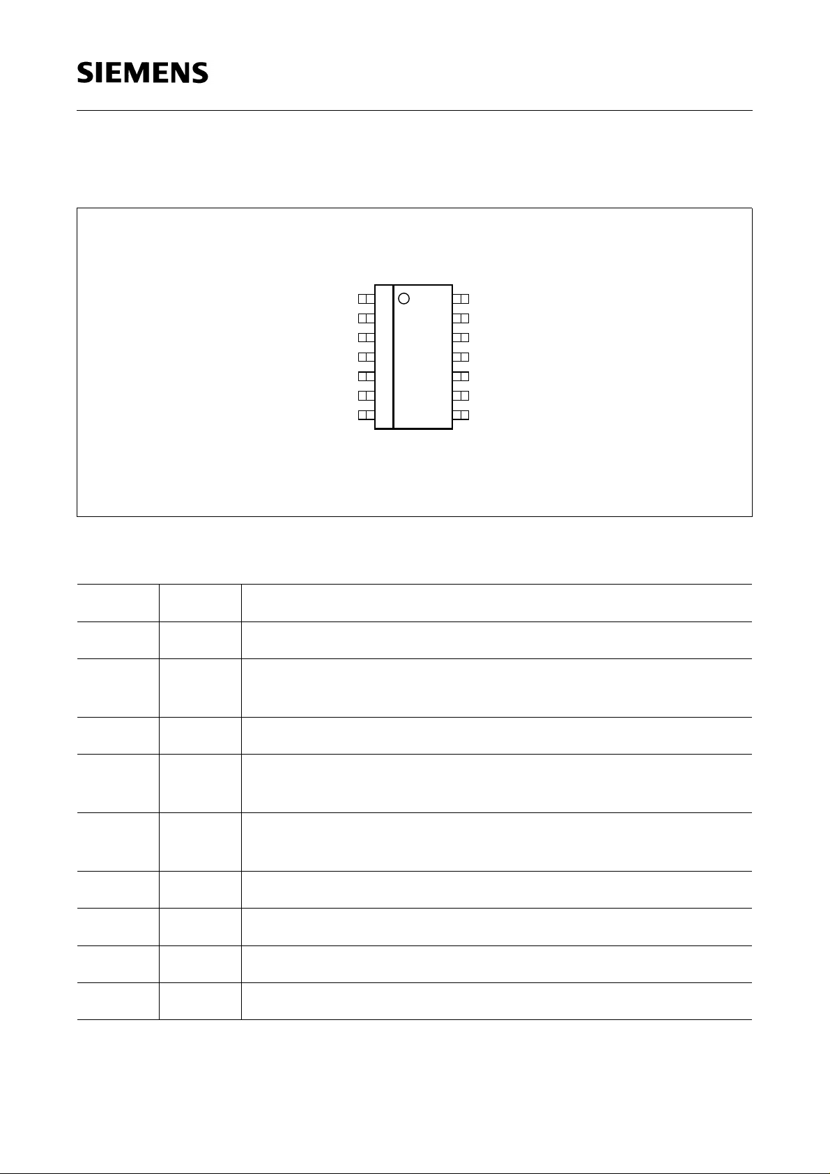
P-DSO-14-4
RE
GND
GND
GND GND
GND
1
2
D
3
4
5
6
7SO
R
14
13
12
11
10
9
8
AEP02248
SI
Ι
GND
GND
Q
Pin Definitions and Functions (TLE 4269 GM)
Pin No. Symbol Function
1REReset Threshold; if not needed connect to GND.
2DReset Delay; connect to GND via external delay capacitor for
setting delay time.
3, 4, 5, 6 GND Ground
7RReset Output; open-collector output, internally connected to Q
via a pull-up resistor of 20 kΩ.
8SOSense Output; open-collector output, internally connected to Q
via a 20 kΩ pull-up resistor.
9Q5-V Output; connect to GND with a 10 µF capacitor, ESR < 10 Ω.
10, 11, 12 GND Ground
13 I Input; block to GND directly at the IC by a ceramic capacitor.
14 SI Sense Input; if not needed connect to Q.
Semiconductor Group 3 1998-11-01

Pin Configuration
(top view)
TLE 4269
P-DSO-20-6
RE
D
N.C.
GND
GND
GND
GND
N.C.
N.C.
R
1
2
3
4
5
6
7
8
9
10
20
19
18
17
16
15
14
13
12
11
AEP01802
Ι
S
Ι
N.C.
GND
GND
GND
GND
N.C.
Q
SO
Pin Definitions and Functions (TLE 4269 GL)
Pin No. Symbol Function
1REReset Threshold; if not needed connect to GND.
2DReset Delay; to select delay time connect to GND via external
capacitor.
4-7, 14-17 GND Ground
10 R Reset Output; the open-collector output is internally linked to
Q via 20 kΩ pull-up resistor.
11 SO Sense Output; the open-collector output is internally linked to
Q via 20 kΩ pull-up resistor.
12 Q Output; connect to GND with a 10 µF capacitor, ESR < 10 Ω.
19 I Input; block directly to GND at the IC by a ceramic capacitor.
20 SI Sense Input; if not needed connect to Q.
Semiconductor Group 4 1998-11-01

TLE 4269
Circuit Description
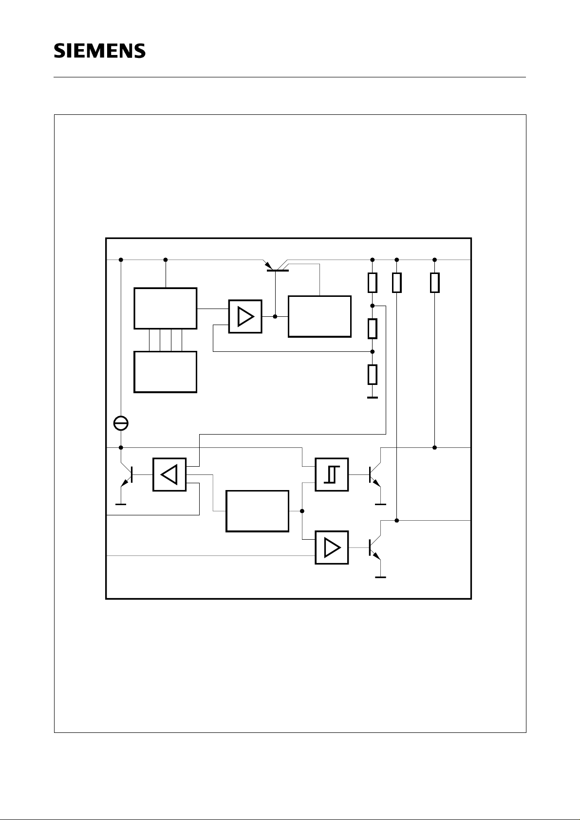
The control amplifier compares a reference voltage, made highly accurate by resistance
balancing, with a voltage propo rtional to the output voltage and drives the base of the
series PNP transistor via a buffe r. Saturation control as a function of the load current
prevents any over-saturation of the power element.
In the reset generator block a comparator compares a reference voltage independent of
the input voltage with the scaled-down output voltage. If the output voltage reaches 4.6 V
the reset delay capaci tor is discharged and the reset output is set to low . This low is
guaranteed down to an output voltage of 1 V. As the output voltage incr eases again,
from 4.6 V onward the reset delay capacitor is charged with constant current. When the
V
capacitor voltage reaches the upper switching threshold
choosing the value of this capaci tor, the reset delay time can be selected over a wide
range. With the reset t hresh old in put RE it is possible to lo we r the res et threshold
pin RE is connected to pin Q vi a a voltage divider, for example, the re set condition is
reached when this voltage is decreased below the switching threshold
, the reset returns to high. By
dT
V
V
of 1.35 V.
re
rt
. If
Another comparator compares the signal of the pin SI, normally fed by a voltage divider
from the input voltage, with the reference and gives an early warning on the pin SO. It is
also possible to superwise an other voltage e.g. of a second regulator, or to build a
watchdog circuit with few external components.
Application Description
C
The input capacitor
approx. 1 Ω in series with
capacita nce c an be damp ed. Th e out put ca pacit or C
is necessary for compensating line influences. Using a resistor of
I
C
, the oscillating circuit consisting of input inductivity and input
I
is necessary for the stability of the
Q
regulating circuit. Stability is guaranteed at values ≥ 10 µF and an ESR ≤ 10 Ω within the
operating temperature rang e. For small tol erances of the rese t delay the s pread of the
capacitance of the delay capacitor and its temperature coefficient should be noted.
Semiconductor Group 5 1998-11-01

TLE 4269
D
RE
Ι
Error
20 kΩΩk20
Q
Amplifier
Reference
Current and
Saturation
Control
Trimming
R
Reference
SO
SI
AEB01669
Block Diagram
Semiconductor Group 6 1998-11-01
 Loading...