

5-V Low-Drop Voltage Regulator TLE 4260
Features
• Low-drop voltage
• Very low quiescent current
• Low starting current consumption
• Integrated temperature protection
• Protection against reverse polarity
• Input voltage up to 42 V
• Overvoltage protection up to 65 V (
• Short-circuit proof
• Suited for automotive electronics
• Wide temperature range
• EMC proofed (100 V/m)
≤ 400 ms)
P-TO220-5-1
Type Ordering Code Package
▼ TLE 4260 Q67000-A8187 P-TO220-5-1
▼ TLE 4260 S Q67000-A9044 P-TO220-5-2
▼ Please also refer to the new pin compatible device TLE 4270
P-TO220-5-2
Functional Description
TLE 4260; S is a 5-V low-drop fixed-voltage regulator in a P-TO220-5-H/S package. The
maximum input voltage is 42 V (65 V/
≤ 400 ms). The device can produce an output
current of more than 500 mA. It is shortcircuit-proof and incorporates temperature
protection that disables the circuit at unpermissibly high temperatures.
Due to the wide temperat ure range o f – 40 to 15 0 °C, the TLE 4260; S i s also s uitable
for use in automotive applications.
V
The IC regulates an input voltage
in the range 6 < VI < 35 V to V
I
signal is generated f or an output voltage of
Qnominal
V
<4.75V. The reset delay can be set
Q
= 5.0 V. A reset
externally with a ca pacitor. If the output current is reduc ed below 10 mA, the regulator
switches internally to standby and the reset generator is turned off. The standby current
drops to max. 700 µA.
Semiconductor Group 1 1998-11-01
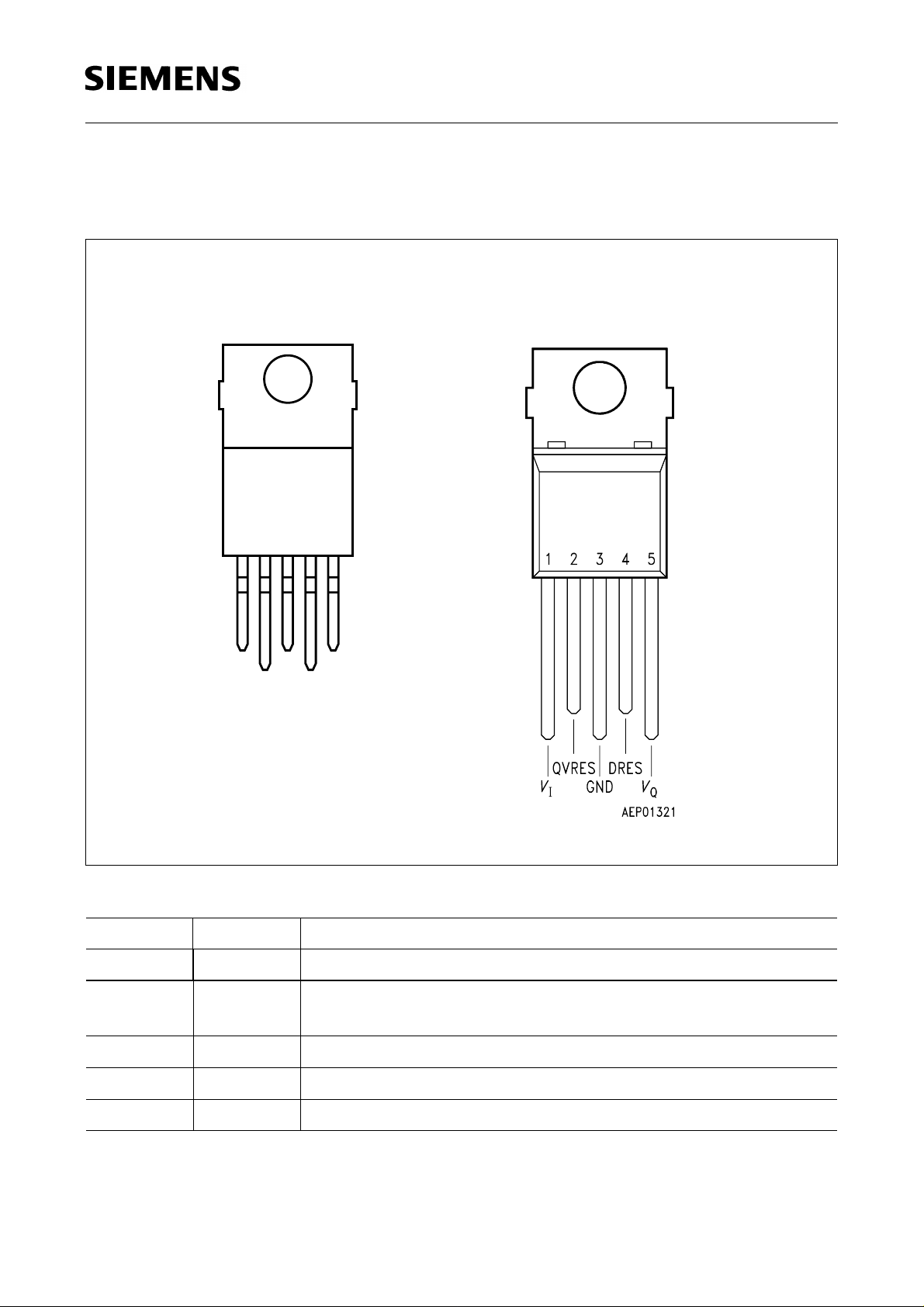
Pin Configuration
AEP00577
12345
V
QVRES
GND
DRES
V
Ι Q
(top view)
TLE 4260
TLE 4260 TLE 4260 S
Pin Definitions and Functions (TLE 4260 and TLE 4260 S)
Pin No. Symbol Function
1
V
I
Input; block directly to ground at the IC by a 470-nF capacitor
2 QVRES Reset output; open collector output controlled by the reset
delay
3GNDGround
4 DRES Reset delay; wired to ground with a capacitor
5
Semiconductor Group 2 1998-11-01
V
Q
5-V output voltage; block to ground with a 22-µF capacitor
TLE 4260
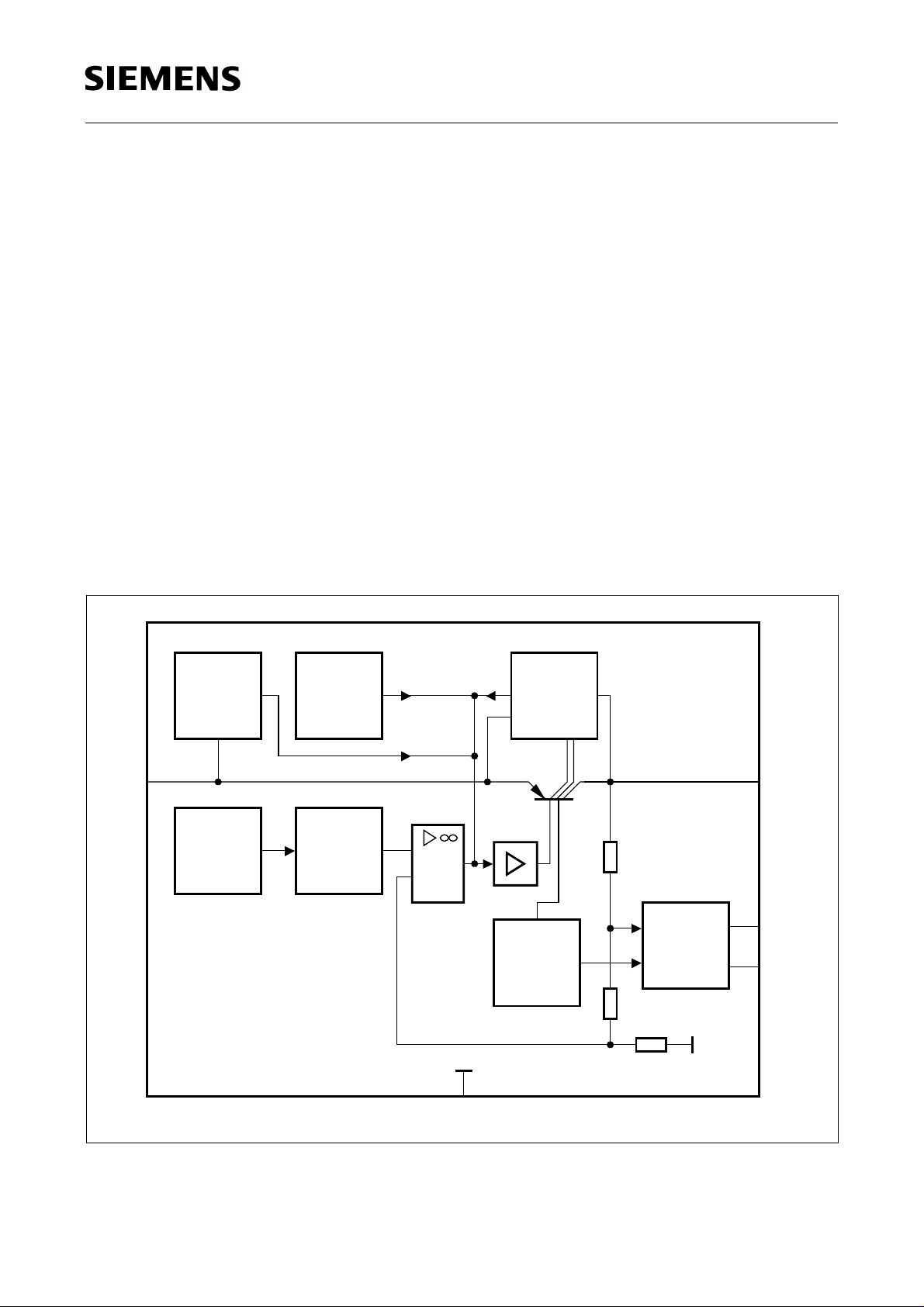
Circuit Description
The control amplifie r compares a reference voltage, which i s kept highly accurate by
resistance adjustment, to a voltag e t hat is proporti onal to the o utput v oltage and d rives
the base of the series transistor via a buffer. Saturat ion control as a function of the load
current prevents any over-sat uration of the power element. If the output vol tage goes
below 96% of its typical value, an external capacitor is discharged on pin 4 by the reset
generator. If the voltage on the capacitor reaches the lower threshold V
is issued on pin 2 and not cancelled again until the upper threshold V
an output current of less than I
QN Off
= 10 mA the standby changeover turns off the reset
generator. The latter is turne d on again when the output current in creases, the output
voltage drops below 4.2 V or the delay capacitor is discharged by external measures.
The IC also incorporates a number of internal circuits for protection against:
•Overload
• Overvoltage
• Overtemperature
• Reverse polarity
, a reset signal
ST
is exceeded. For
DT
Input
Overvoltage
Monitoring
1
Adjustment
Temperature
Sensor
BANDGAP
Reference
Control
Amplifier
+
-
GND
Buffer
STANDBY
Changeover
3
Saturation
Control and
Protection
Circuit
RESET
Generator
7
4
2
AEB00578
Output
RESET
Delay
RESET
Block Diagram
Semiconductor Group 3 1998-11-01
Absolute Maximum Ratings
Parameter Symbol Limit Values Unit Remarks
min. max.
Input (Pin 1)
TLE 4260
Input voltage
Input current
Reset Output (Pin 2)
Voltage
Current
Ground (Pin 3)
Current
Reset Delay (Pin 4)
Voltage
Current
V
V
I
I
V
I
R
I
GND
V
I
D
I
I
– 42 42 V –
–65Vt ≤ 400 ms
–1.6A–
R
– 0.3 42 V –
– – – internally limited
–0.5 – A –
D
– 0.3 42 V –
– – – internally limited
Output (Pin 5)
Differential voltage
Current
V
I
Q
I
– V
–5.25 V
Q
I
–1.4A–
V–
Temperature
Junction temperature
Storage temperature
Semiconductor Group 4 1998-11-01
T
j
T
stg
–32°C–
– 50 150 °C–
Operating Range
Parameter Symbol Limit Values Unit Remarks
min. max.
Input voltage
V
I
–32V
1)
TLE 4260
Junction temperature T
j
Thermal Resistances
Junction ambient
Junction case
1)
See diagram “Output Curren t vers us In put Voltage”
R
R
thja
thjc
– 40 165 °C–
–65K/W–
– 3 K/W –
Semiconductor Group 5 1998-11-01
 Loading...