

1-A Quad-HBD (Quad-Half-Bridge Driver) TLE 4208
Overview
Features
• Driver for up to 3 motors
• Delivers up to 0.8 A continuous
• Optimized for DC motor management applications
• Very low current consumption
in stand-by (Inhibit) mode
• Low saturation voltage
• Output protected against short circuit
• Error flag diagnosis
• Overvoltage lockout and diagnosis
• Undervoltage lockout
• CMOS/TTL compatible inputs with hysteresis
• No crossover current
• Internal clamp diodes
• Overtemperature protection with hysteresis and diagnosis
• Enhanced power P-DSO-Package
; typ.1.2 V total @ 25 °C; 0.4 A
P-DSO-28-6
Type Ordering Code Package
TLE 4208 G Q67007-A9335 P-DSO-28-6
Description
The TLE 4208 is a fully protected Quad-Half-Bridge-Driver designed specially for
automotive and industrial motion control applications.
The part is built using the Siemens bipolar high voltage power technology DOPL.
In a cascade configuration up to three actuators (DC motors) can be connected between
the four half-bridges. These four half-bridges are configured as 2 dual-half-bridges,
which are supplied and controlled separately. Operation modes forward (cw), reverse
(ccw), brake and high impedance are invoked from a standard interface.
The standard enhanced power P-DSO-28 package meets the application requirements
and saves PCB-board space and costs.
Furthermore the built-in features like diagnosis, over- and undervoltage-lockout, shortcircuit protection, over-temperature protection and the very low quiescent current in
stand-by mode will open a wide range of automotive and industrial applications.
Semiconductor Group 1 1998-06-03
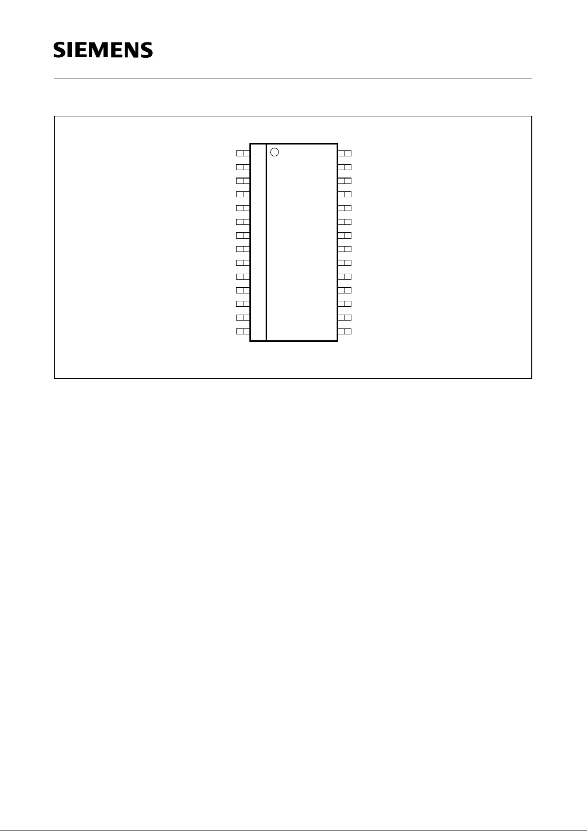
TLE 4208
GND
EF
IN1
N.C.
OUT1
GND
GND
GND
GND
OUT3
N.C.
IN3
INH
GND
128
2
12
3
4
5
6
7
TLE 4208 G
8
9
10
11
12
13
34
14
Figure 1 Pin Configuration (top view)
27
26
25
24
23
22
21
20
19
18
17
16
15
N.C.
INH
12
IN2
V
S12
OUT2
GND
GND
GND
GND
OUT4
V
S34
IN4
EF
34
N.C.
AEP02349
Semiconductor Group 2 1998-06-03
Pin Definitions and Functions
Pin No. Symbol Function
TLE 4208
1, 6, 7, 8, 9,
14, 20, 21,
GND Ground;
negative reference potential for blocking capacitor
22, 23
2EF
12
Error Flag output of half-bridges 1and 2;
open collector; low = error
3 IN1 Input channel of half-bridge 1;
controls OUT1
4, 11, 15, 28 N.C. Not connected
5 OUT1 Power output of half-bridge 1;
full short circuit protected; with integrated clamp diodes
10 OUT3 Power output of half-bridge 3;
full short-circuit protected; with integrated clamp diodes
12 IN3 Input channel of half-bridge 3;
controls OUT3
13 INH
34
Inhibit input of half-bridges 3 and 4;
low = half-bridges 3 and 4 in stand-by
16 EF
34
Error Flag output of half-bridges 3 and 4;
open collector; low = error
17 IN4 Input channel of half-bridge 4;
controls OUT4
18
V
S34
Power supply voltage of half-bridges 3 and 4;
positive reference potential for blocking capacitor
19 OUT4 Power output of half-bridge 4;
full short circuit protected; with integrated clamp diodes
24 OUT2 Power-output of half-bridge 2;
full short circuit protected; with integrated clamp diodes
25
V
S12
Power supply voltage of half-bridges 1 and 2;
positive reference potential for blocking capacitor
26 IN2 Input channel of half-bridge 2;
controls OUT2
27 INH
12
Inhibit input of half-bridges 1and 2;
low = half-bridges 1 and 2 in stand-by
Semiconductor Group 3 1998-06-03
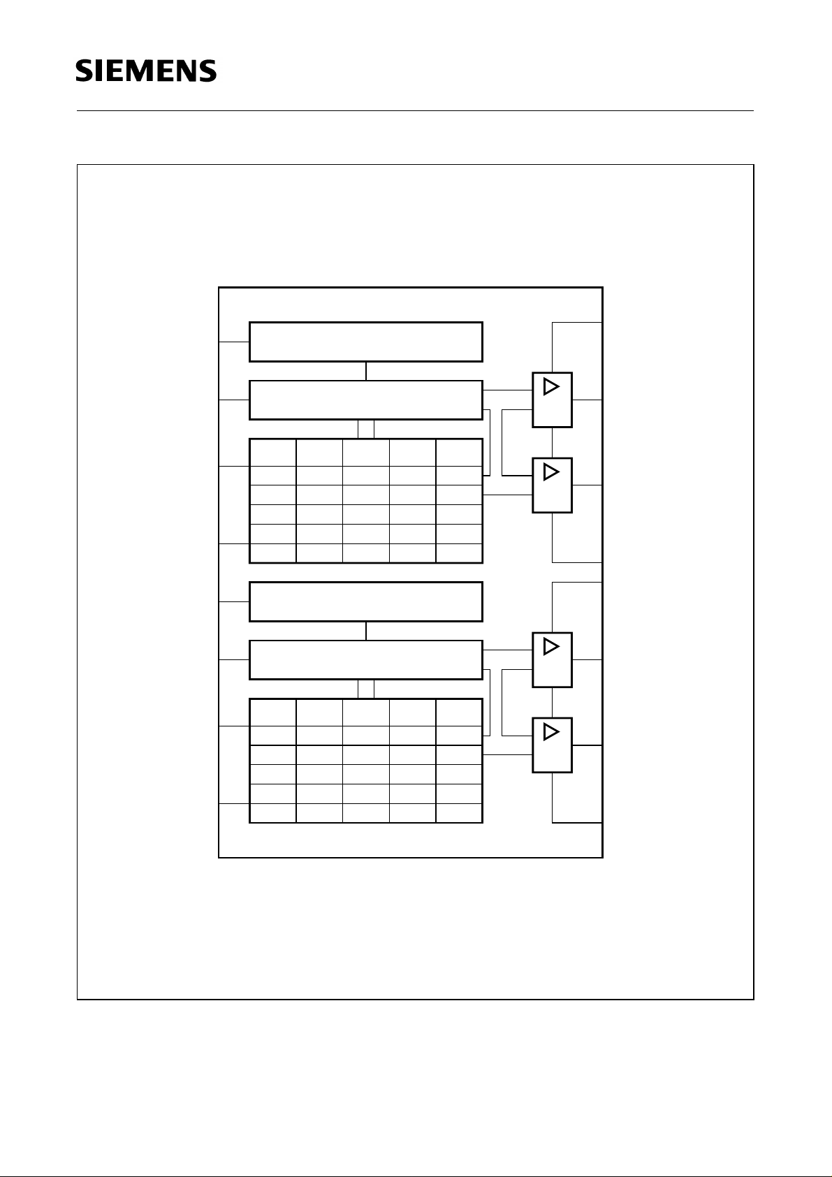
TLE 4208
INH
EF
INH
EF
12
12
IN1
IN2
34
34
IN3
IN4
27
2
3
26
13
16
12
17
INH
0
1
1
1
INH
0
1
1
1
1
Inhibit 1,2
Fault-Detection 1,2
IN1 IN2
12
0
0
1
1
Inhibit 3,4
Fault-Detection 3,4
34
IN3
IN4
X
0
0
1
1
0
1
0
11
X
0
1
0
1
TLE 4208 G
OUT1 OUT2
ZXZX
L
L
H
H
OUT3
Z
L
L
H
L
H
OUT4
Z
L
LH
H
H
L
H
DRV1
DRV2
DRV3
DRV4
25
5
24
1,6,7,8,
9,14,
20,21,
22,23
10
19
18
V
S12
OUT1
OUT2
GND
OUT3
OUT4
V
S34
AEB02350
Figure 2 Block Diagram
Semiconductor Group 4 1998-06-03
Input Logic
Functional Truth Table of Halfbridge 1 and 2
TLE 4208
INH
12
IN1 IN2 OUT1 OUT2 Mode
0 X X Z Z Stand-By
1
1
1
1
0
0
1
1
0
1
0
1
L
L
H
H
L
H
L
H
Brake LL
CW
CCW
Brake HH
Note: Half-Bridge 1 and 2 connected to a full-bridge
Functional Truth Table of Half-Bridge 3 and 4
INH
34
IN3 IN4 OUT3 OUT4 Mode
0 X X Z Z Stand-By
1
1
1
1
0
0
1
1
0
1
0
1
L
L
H
H
L
H
L
H
Brake LL
CW
CCW
Brake HH
IN: 0 = Logic LOW OUT: Z = Output in tristate condition
1 = Logic HIGH L = Output in sink condition
X = don’t care H = Output in source condition
Note: Half-Bridge 3 and 4 connected to a full-bridge
Diagnosis
EF
1
0
0
1
1
0
0
12
EF
1
1
1
0
0
0
0
34
Error
no error
over temperature of half-bridge 1 and 2 or
over voltage of half-bridge 1 and 2
over temperature of half-bridge 3 and 4 or
over voltage of half-bridge 3 and 4
over temperature of all half-bridges or
over voltage of all half-bridges
Semiconductor Group 5 1998-06-03
 Loading...