

Siemens SFH6318, SFH6319 Datasheet
SFH6318
SFH6319
LOW CURRENT, HIGH GAIN
OPTOCOUPLER
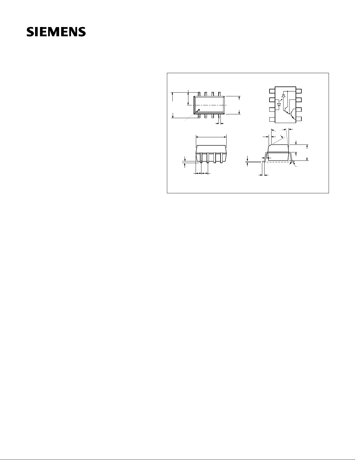
Package Dimensions in Inches (mm)
.120±.002
FEATURES
• Industry Standard SOIC-8 Surface Mountable
Package
• High Current Transfer Ratio, 800%
• Low Input Current, 0.5mA
• High Output Current, 60mA
• Isolation T est V oltage, 2500 VA CRMS
• TTL Compatible Output, VOL=0.1 V
• Adjustable Bandwidth-Access to Base
• Underwriters Lab File #E52744
APPLICATIONS
• Logic Ground Isolation-TTL/TTL, TTL/CMOS,
CMOS/CMOS, CMOS/TTL
• EIA RS 232C Line Receiver
• Low Input Current Line Receiver-Long Lines,
Party Lines
• Telephone Ring Detector
• 117 VAC Line Voltage Status Indication-Low
Input Power Dissipation
• Low Power Systems-Ground Isolation
DESCRIPTION
Very high current ratio together with 2500 VAC isolation
are achieved b y coupling an LED with an integ r ated high
gain photodetector in a SOIC-8 package. Separate pins
for the photodiode and output stage enable TTL compatible saturation voltages with high speed operation. Photodarlington operation is achieved by tying the VCC and
VO terminals together. Access to the base terminal
allows adjustment to the gain bandwidth.
The SFH6318 is ideal for TTL applications since the
300% minimum current transfer ratio with an LED current
of 1.6 mA enables operation with one unit load-in and
one unit load-out with a 2.2 KW pull-up resistor.
The SFH6319 is best suited for low power logic applications involving CMOS and low power TTL. A 400% current transfer ratio with only 0.5 mA of LED current is
guaranteed from 0 ° C to 70 ° C.
Caution:
Due to the small geometries of this device, it should be handled
with Electrostatic Discharge (ESD) precautions. Proper grounding would prevent damage further and/or degradation which
may be induced by ESD.
(3.05±.05)
.154±.002
.240
(6.10)
Pin 1
.004 (.10)
.008 (.20)
.021
(.53)
.192±.005
(4.88±.13)
.050
(1.27)
typ.
C
L
(.391±.05)
.016
(.41)
.015±.002
.008 (.20)
.020±.004
(.15±.10)
2 plcs.
TOLERANCE: ±.005 (unless otherwise noted)
Maximum Ratings (25 ° )
Emitter
Reverse Input V oltage....................................................................... 3 V
Supply and Output Voltage, VCC (pin 8-5), VO (pin 6-5)
SFH6318........................................................................... –0.5 to 7 V
SFH6319......................................................................... –0.5 to 18 V
Input Power Dissipation ..............................................................35 mW
Derate Linearly above 50 ° C
Free Air Temperature.........................................................0.7 mW/ ° C
Average Input Current..................................................................20 mA
Peak Input Current.......................................................................40 mA
(50% Duty Cycle-1 ms pulse width)
Peak Transient Input Current
(tp ≤ 1 µ sec, 300 pps) ..................................................................1.0 A
Detector (Si Photodiode + Photodarlington)
Output Current IO (pin 6).............................................................60 mA
Emitter-Base Reverse Voltage (pin 5-7).........................................0.5 V
Output Power Dissipation .........................................................150 mW
Derate Linearly from 25 ° C ...................................................2 mW/ ° C
Package
Storage Temperature.................................................. –55 ° C to +125 ° C
Operating Temperature................................................. –40 ° C to +85 ° C
Lead Soldering Temperature (t=10 sec.) ..................................... 260 ° C
Junction Temperature .................................................................. 100 ° C
Ambient T emper ature Range...................................... –55 ° C to +100 ° C
Isolation T est Voltage between
Emitter and Detector...................................................2500 VACRMS
(refer to climate DIN 40046, part 2, Nov. 74)
Pollution Degree (DIN VDE 0110).........................................................2
Creepage Distance...................................................................... ≥ 4 mm
Clearance .................................................................................... ≥ 4 mm
Comparative Tracking Index
per DIN IEC 112/VDE 0303, part 1.............................................. 175
Isolation Resistance
VIO=500 V, T A=25 ° C RISOL................................................. ≥ 1012W
VIO=500 V, T A=100 ° C RISOL............................................... ≥ 1011W
Anode
Cathode
(.38±.05)
NC
NC
1
2
3
4
40°
5° max.
R.010
max.
(.25)
8
VCC
7
VB
6
V
GND
5
7°
.058±.005
(1.49±.13)
.125±.005
(3.18±.13)
Lead
Coplanarity
±.0015 (.04)
max.
0
1

=0 °
≅
µ
µ
∆
/ ∆
°
µ
µ
Electro-Optical Characteristics (T
C to 70 ° C, T
A
=25 ° C-Typical, unless otherwise specified)
A
Parameter Symbol Device Min Typ Max Units Test Conditions Note
Current Transfer Ratio CTR SFH6318 300 1600 2600 % I
Logic Low
Output Voltage
Logic High
Output Current
Logic Low Supply Current I
Logic High Supply Current I
Input Forward Voltage V
Temperature Coefficient,
Forward Voltage
Input Capacitance C
Resistance (Input-Output) R
Capacitance (Input-Output) C
Switching Specifications (T
=25 ° C)
A
V
I
OH
CCL
CCH
OL
F
V
IN
I-O
I-O
SFH6319 400
SFH6318 0.1 0.4 V I
SFH6319 0.1
SFH6318 0.1 250 µ AI
SFH6319 0.05 100
T
F
A
500
1600
2000
0.15
0.25
2600
3500
0.4
0.4
0.4
%I
VI
AI
0.2 1.5 mA I
0.01 10
AI
1.4 1.7 V I
–1.8 mV/
C
25 pF f=1 MHz, V
12
10
10
11
Ω
Ω
0.6 pF f=1 MHz 3
=1.6 mA, V
F
=0.5 mA, V
F
I
=1.6 mA, V
F
=1.6 mA, I
F
=1.6 mA, I
F
I
=5 mA, I
F
I
=12 mA, I
F
=0 mA, V
F
=0 mA, V
F
=1.6 mA, V
F
=0 mA, V
F
=1.6 mA, T
F
=1.6 mA
I
F
V
=500 VDC, T
IO
V
=500 VDC, T
IO
=0.4 V, V
O
=0.4 V, V
O
=0.4 V, V
O
=4.8 mA, V
O
=8 mA, V
O
=15 mA, V
O
=24 mA, V
O
=V
=7 V 2
O
CC
=V
=18 V 2
O
CC
=OPEN, V
O
=OPEN, V
O
=25 ° C
A
=0
F
=25 ° C
A
=100 ° C
A
=4.5 V 1,2
CC
=4.5 V
CC
=4.5 V
CC
=4.5 V2
CC
=4.5 V
CC
=4.5 V
CC
=4.5 V
CC
=18 V2
CC
=18 V 2
CC
Parameter Symbol Device Min Typ Max Units Test Conditions Note
1,2
2
3
Propagation Delay Time
To Logic Low at Output
Propagation Delay Time
To Logic High at Output
Common Mode Transient Immunity
at Logic High Level Output
Common Mode Transient Immunity
at Logic Low Level Output
t
PHL
t
PLH
| CM
| CM
SFH6318 2 10
SFH6319 6
0.6
25
1
sI
sI
SFH6318 2 35 µsI
SFH6319 4
1.5
|1 KV/µsI
H
|1 KV/µsI
L
60
7
µsI
=1.6 mA, R
F
=0.5 mA, R
F
I
=12 mA, RL=270 Ω
F
=1.6 mA, RL=2.2 KΩ
F
=0.5 mA, RL=4.7 KΩ
F
I
=12 mA, RL=270 Ω
F
=0 mA, RL=2.2 KΩ
F
V
=10 V
CM
=1.6 mA, RL=2.2 KΩ
F
V
=10 V
CM
Notes
1. DC current transfer ratio is defined as the ratio of output collector current, I
, to the forward LED input current, I
O
times 100%.
F
2. Pin 7 open.
3. Device considered a two-terminal device: pins 1, 2, 3 and 4 shorted together and pins 5, 6, 7 and 8 shorted together.
4. Using a resistor between pin 5 and 7 will decrease gain and delay time.
5. Common mode transient immunity in logic high level is the maximum tolerable (positive) dV
V
, to assure that the output will remain in a logic high state (i.e. V
CM
tolerable (negative) dV
(i.e. V
<0.8 V).
O
/dt on the trailing edge of the common mode pulse signal, V
cm
>2.0 V) common mode transient immunity in logic low level is the maximum
O
CM
6. In applications where dv/dt may exceed 50,000 V/ µ s (such as state discharge) a series resistor, R
(mA)
F
k Ω .
Refer to Figure 2.
tively high surge currents. The recommended value is
R
CC
IV
0.15 I
/dt on the leading edge of the common mode pulse,
cm
, to assure that the output will remain in a logic low state
should be included to protect IC from destruc
CC
p-p
p-p
=2.2 K Ω
L
=4.7 KΩ
L
2,4
2,4
5,6
5,6
2
SFH6318/6319
 Loading...