

Siemens SAB80C537-M, SAB80C537-M-T40-85, SAB80C537-M16, SAB80C537-N, SAB80C517-16-N-T40-85 Datasheet
...
Microcomputer Components
8-Bit CMOS Single-Chip Microcontroller
SAB 80C517/80C537
Data Sheet 04.95

High-Performance SAB 80C517/80C537
8-Bit CMOS Single-Chip Microcontroller
Advanced Information
SAB 80C517 Microcontroller with factory mask-programmable ROM
SAB 80C537 Microcontroller for external ROM
● Versions for 12 MHz and 16 MHz ● Fast 32-bit division, 16-bit 2 multiplication,
operating frequency 32-bit normalize and shift by peripheral
● 8 K × 8 ROM (SAB 80C517 only) MUL/DIV unit (MDU)
● 256 × 8 on-chip RAM ● Eight data pointers for external memory
● Superset of SAB 80C51 architecture: addressing
1µs instruction cycle time at 12 MHz
750 ns instruction cycle time at 16 MHz levels selectable
256 directly addressable bits
Boolean processor inputs and programmable ref. voltages
64 Kbyte external data and program
memory addressing
● Four 16-bit timer/counters ● Extended power saving modes
● Powerful 16-bit compare/capture unit ● Nine ports: 56 I/O lines, 12 input lines
(CCU) with up to 21 high-speed or PWM
output channels and 5 capture inputs 0 to 70
● Versatile "fail-safe" provisions – 40 to 85
● Fourteen interrupt vectors, four priority
● 8-bit A/D converter with 12 multiplexed
● Two full duplex serial interfaces
● Fully upward compatible with SAB 80C515
● Two temperature ranges available:
o
C
o
C
● Plastic packages: P-LCC-84,
P-MQFP-100-2
SAB 80C517/80C537
Semiconductor Group 1 04.95

SAB 80C517/80C537
The SAB 80C517/80C537 is a high-end member of the Siemens SAB 8051 family of
microcontrollers. It is designed in Siemens ACMOS technology and based on the SAB 8051
architecture. ACMOS is a technology which combines high-speed and density characteristics
with low-power consumption or dissipation.
While maintaining all the SAB 80C515 features and operating characteristics the
SAB 80C517 is expanded in its arithmetic capabilities, "fail-safe" characteristics, analog signal
processing and timer capabilities. The SAB 80C537 is identical with the SAB 80C517 except
that it lacks the on-chip program memory. The SAB 80C517/SAB 80C537 is supplied in a
84 pin plastic leaded chip carrier package (P-LCC-84) and in a 100-pin plastic quad metric flat
package (P-MQFP-100-2).
Ordering Information
Type Ordering Code Package Description
8-bit CMOS Microcontroller
SAB 80C517-N Q67120-C397 P-LCC-84
SAB 80C517-M TBD P-MQFP-100-2
SAB 80C537-N Q67120-C452 P-LCC-84
SAB 80C537-M TBD P-MQFP-100-2
SAB 80C517-N-T40/85 Q67120-C483 P-LCC-84 with factory mask-programmaSAB 80C517-M-T40/85 TBD P-MQFP-100-2
SAB 80C537-N-T40/85 Q67120-C484 P-LCC-84
SAB 80C537-M-T40/85 TBD P-MQFP-100-2
SAB 80C517-N16 Q67120-C723 P-LCC-84 with mask-programmable
SAB 80C517-M16 TBD P-MQFP-100-2
SAB 80C537-N16 Q67120-C722 P-LCC-84
SAB 80C537-M16 TBD P-MQFP-100-2
SAB 80C517-N16-T40/85 Q67120-C724 P-LCC-84 with mask-programmable ROM,
with factory mask-programmable ROM, 12 MHz
for external memory, 12 MHz
ble ROM, 12 MHz,
ext. temperature – 40 to 85 °C
for external ROM, 12 MHz,
ext. temperature – 40 to 85 °C
ROM,16 MHz ext. temperature
– 40 to 110 °C
for external memory, 16 MHz
16 MHz
ext. temperature – 40 to 85 °C
SAB 80C517-16-N-T40/85 Q67120-C725 P-LCC-84 with factory mask-programma-
ble ROM, 12 MHz
Semiconductor Group 2

SAB 80C517/80C537
Logic Symbol
Semiconductor Group 3
SAB 80C517/80C537
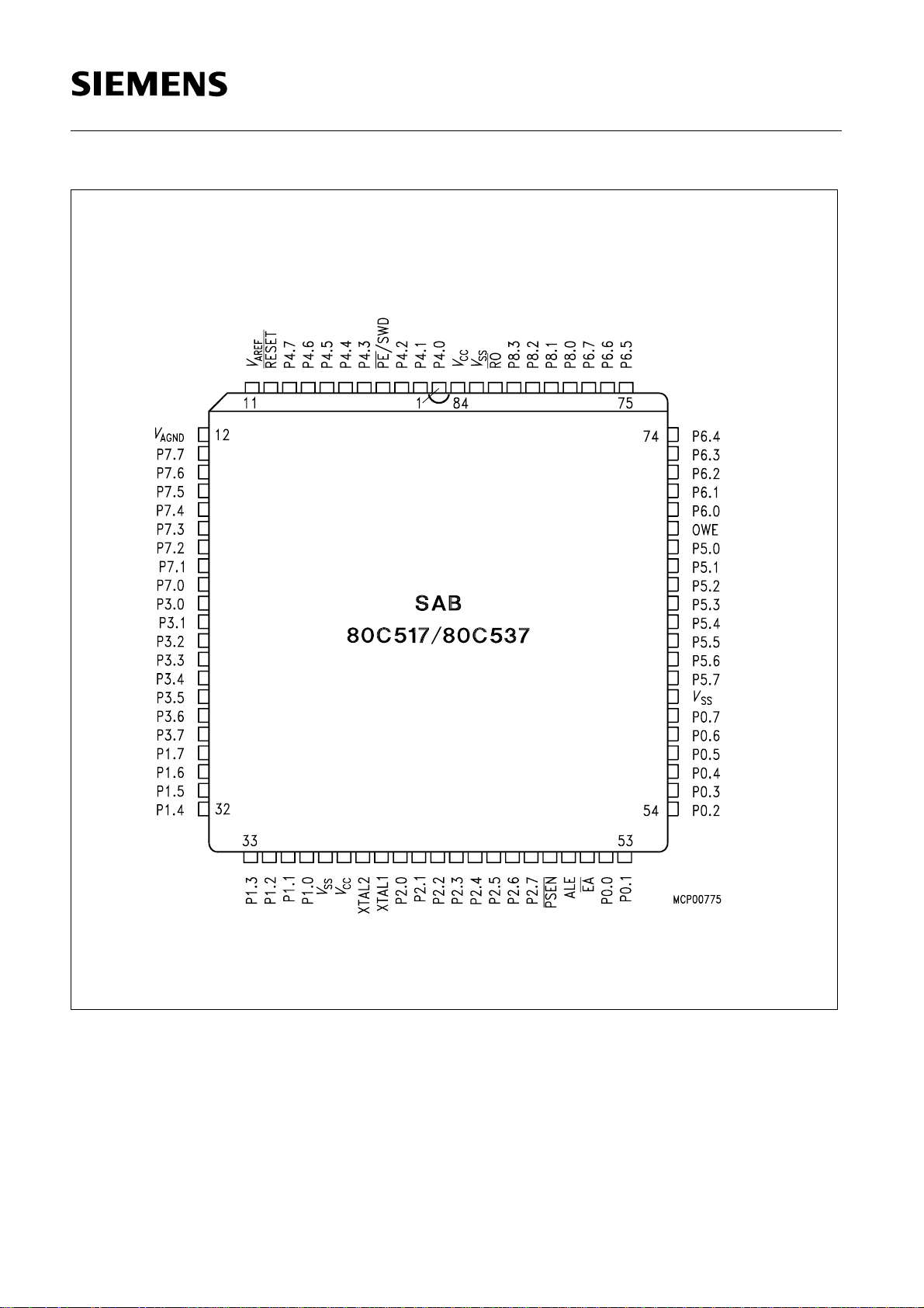
Pin Configuration
(P-LCC-84)
Semiconductor Group 4

SAB 80C517/80C537
Pin Configuration
(P-MQFP-100-2)
Semiconductor Group 5

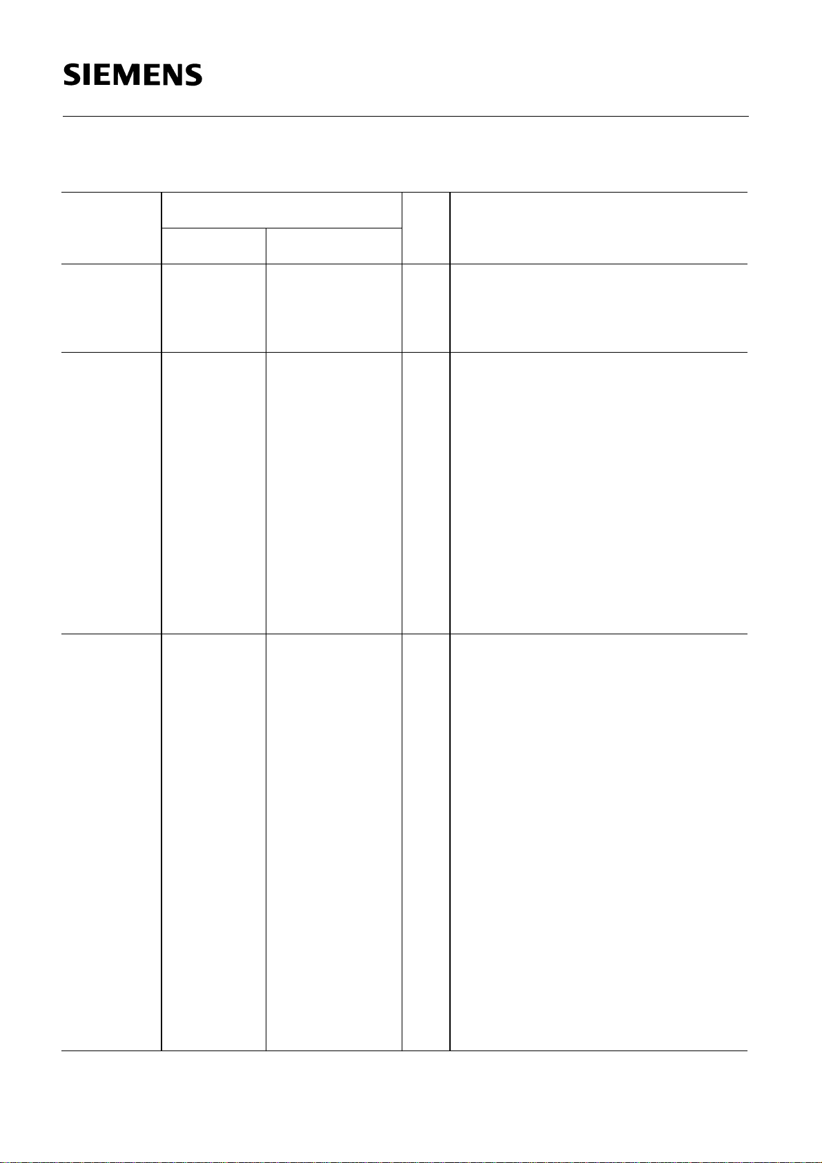
Pin Definitions and Functions
Symbol Pin Number
P-LCC-84 P-MQFP-100-2
I/O
*)
Function
SAB 80C517/80C537
P4.0 – P4.7 1– 3, 5 – 9 64 - 66,
68 - 72
I/O Port 4
is a bidirectional I/O port with internal
pull-up resistors. Port 4 pins that have
1 s written to them are pulled high by
the internal pull-up resistors, and in that
state can be used as inputs. As inputs,
port 4 pins being externally pulled low
will source current (I
characteristics) because of the internal
pull-up resistors.
This port also serves alternate compare
functions. The secondary functions are
assigned to the pins of port 4 as
follows:
– CM0 (P4.0): Compare Channel 0
– CM1 (P4.1): Compare Channel 1
– CM2 (P4.2): Compare Channel 2
– CM3 (P4.3): Compare Channel 3
– CM4 (P4.4): Compare Channel 4
– CM5 (P4.5): Compare Channel 5
– CM6 (P4.6): Compare Channel 6
– CM7 (P4.7): Compare Channel 7
in the DC
IL,
PE/SWD 4 67 I Power saving modes enable/
Start Watchdog Timer
A low level on this pin allows the
software to enter the power down, idle
and slow down mode. In case the low
level is also seen during reset, the
watchdog timer function is off on
default.
Use of the software controlled power
saving modes is blocked, when this pin
is held on high level. A high level during
reset performs an automatic start of the
watchdog timer immediately after reset.
When left unconnected this pin is pulled
high by a weak internal pull-up resistor.
*
I = Input
O = Output
Semiconductor Group 6

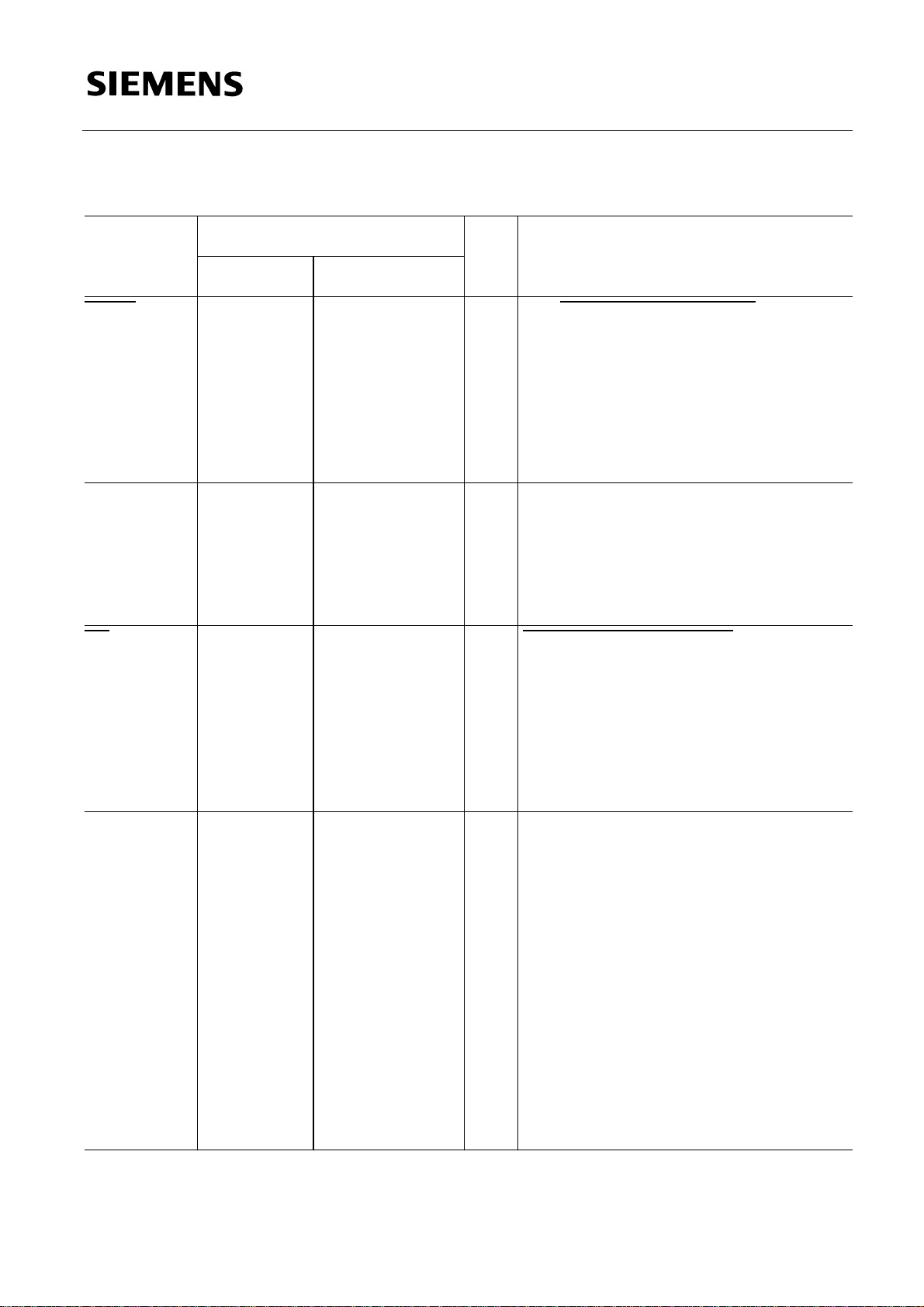
Pin Definitions and Functions (cont’d)
Symbol Pin Number
I/O
Function
*)
P-LCC-84 P-MQFP-100-2
RESET 10 73 I RESET
A low level on this pin for the duration of
one machine cycle while the oscillator is
running resets the SAB 80C517. A small
internal pull-up resistor permits
power-on reset using only a capacitor
connected to
SAB 80C517/80C537
V
.
SS
V
AREF
11 78 Reference voltage for the A/D con-
verter.
V
AGND
12 79 Reference ground for the A/D
converter.
P7.7 -P7.0 13 - 20 80 - 87 I Port 7
is an 8-bit unidirectional input port. Port
pins can be used for digital input, if
voltage levels meet the specified input
high/low voltages, and for the lower
8-bit of the multiplexed analog inputs of
the A/D converter, simultaneously.
*
I = Input
O = Output
Semiconductor Group 7

Pin Definitions and Functions (cont’d)
Symbol Pin Number
I/O
Function
*)
P-LCC-84 P-MQFP-100-2
P3.0 - P3.7 21 - 28 90 - 97 I/O Port 3
is a bidirectional I/O port with internal
pull-up resistors. Port 3 pins that have
1 s written to them are pulled high by
the internal pull-up resistors, and in that
state can be used as inputs. As inputs,
port 3 pins being externally pulled low
will source current (I
characteristics) because of the internal
pull-up resistors. Port 3 also contains
the interrupt, timer, serial port 0 and
external memory strobe pins that are
used by various options. The output
latch corresponding to a secondary
function must be programmed to a one
(1) for that function to operate.
The secondary functions are assigned
to the pins of port 3, as follows:
SAB 80C517/80C537
in the DC
IL,
*
I = Input
O = Output
–R× D0 (P3.0): receiver data input
(asynchronous) or data input/output
(synchronous) of serial interface
–T× D0 (P3.1): transmitter data
output (asynchronous) or clock
output (synchronous) of serial
interface 0
INT0 (P3.2): interrupt 0 input/timer 0
–
gate control
– INT1 (P3.3): interrupt 1 input/timer 1
gate control
– T0 (P3.4): counter 0 input
– T1 (P3.5): counter 1 input
–
WR (P3.6): the write control signal
latches the data byte from port 0 into
the external data memory
RD (P3.7): the read control signal
–
enables the external data
memory to port 0
Semiconductor Group 8

Pin Definitions and Functions (cont’d)
Symbol Pin Number
P-LCC-84 P-MQFP-100-2
I/O
*)
Function
SAB 80C517/80C537
P1.7 - P1.0 29 - 36 98 - 100,
1, 6 - 9
I/O Port 1
is a bidirectional I/O port with internal
pull-up resistors. Port 1 pins that have
1 s written to them are pulled high by
the internal pull-up resistors, and in that
state can be used as inputs. As inputs,
port 1 pins being externally pulled low
will source current (I
characteristics) because of the internal
pull-up resistors. It is used for the low
order address byte during program
verifi-cation. It also contains the
interrupt, timer, clock, capture and
compare pins that are used by various
options. The output latch must be
programmed to a one (1) for that
function to operate (except when used
for the compare functions).
The secondary functions are assigned
to the port 1 pins as follows:
INT3/CC0 (P1.0): interrupt 3 input/
–
compare 0 output / capture 0 input
– INT4/CC1 (P1.1): interrupt 4 input /
compare 1 output /capture 1 input
– INT5/CC2 (P1.2): interrupt 5 input /
compare 2 output /capture 2 input
– INT6/CC3 (P1.3): interrupt 6 input /
compare 3 output /capture 3 input
– INT2/CC4 (P1.4): interrupt 2 input /
compare 4 output /capture 4 input
– T2EX (P1.5): timer 2 external reload
trigger input
– CLKOUT (P1.6): system clock
output
– T2 (P1.7): counter 2 input
, in the DC
IL
*
I = Input
O = Output
Semiconductor Group 9
Pin Definitions and Functions (cont’d)
Symbol Pin Number
I/O
Function
*)
P-LCC-84 P-MQFP-100-2
XTAL2 39 12 – XTAL2
Input to the inverting oscillator amplifier
and input to the internal clock generator
circuits.
XT AL1 40 13 – XTAL1
Output of the inverting oscillator
amplifier. To drive the device from an
external clock source, XTAL2 should
be driven, while XTAL1 is left
unconnected. There are no
requirements on the duty cycle of the
external clock signal, since the input to
the internal clocking circuitry is devided
down by a divide-by-two flip-flop.
Minimum and maximum high and low
times as well as rise/fall times specified
in the AC characteristics must be
observed.
SAB 80C517/80C537
P2.0 - P2.7 41 - 48 14 - 21 I/O Port 2
is a bidirectional I/O port with internal
pull-up resistors. Port 2 pins that have
1 s written to them are pulled high by
the internal pull-up resistors, and in that
state can be used as in-puts. As inputs,
port 2 pins being externally pulled low
will source current (I
characteristics) because of the internal
pull-up resistors. Port 2 emits the highorder address byte during fetches from
external program memory and during
accesses to external data memory that
use 16-bit addresses (MOVX @DPTR).
In this application it uses strong
internal pull-up resistors when issuing
1 s. During accesses to external data
memory that use 8-bit addresses
(MOVX @Ri), port 2 issues the
contents of the P2 special function
register.
, in the DC
IL
*
I = Input
O = Output
Semiconductor Group 10
SAB 80C517/80C537
Pin Definitions and Functions (cont’d)
*)
Symbol Pin Number
I/O
P-LCC-84 P-MQFP-100-2
PSEN 49 22 O The Program Store Enable
ALE 50 23 O The Address Latch Enable
Function
output is a control signal that enables
the external program memory to the
bus during external fetch operations. It
is activated every six oscillator periodes
except during external data memory
accesses. Remains high during internal
pro-gram execution.
output is used for latching the address
into external memory during normal
operation. It is activated every six
oscillator periodes except during an
external data memory access
EA 51 24 I External Access Enable
When held at high level, instructions
are fetchedfrom the internal ROM
when the PC is less than 8192. When
held at low level, the SAB 80C517
fetches all instructions from external
program memory. For the SAB 80C537
this pin must be tied low
P0.0 - P0.7 52 - 59 26 - 27,
30 - 35
I/O Port 0
is an 8-bit open-drain bidirectional I/O
port. Port 0 pins that have 1 s written to
them float, and in that state can be
used as high-impedance inputs. Port 0
is also the multiplexed low-order
address and data bus during accesses
to external program or data memory. In
this application it uses strong internal
pull-up resistors when issuing 1 s.
Port 0 also outputs the code bytes
during program verification in the
SAB 83C517. External pull-up resistors
are required during program
verification.
*
I = Input
O = Output
Semiconductor Group 11

Pin Definitions and Functions (cont’d)
Symbol Pin Number
I/O
Function
*)
P-LCC-84 P-MQFP-100-2
P5.7 - P5.0 61 - 68 37 - 44 I/O Port 5
is a bidirectional I/O port with internal
pull-up resistors. Port 5 pins that have
1 s written to them are pulled high by
the internal pull-up resistors, and in that
state can be used as inputs. As inputs,
port 5 pins being externally pulled low
will source current (I
characteristics) because of the internal
pull-up resistors. This port also serves
the alternate function "Concurrent
Compare". The secondary functions
are assigned to the port 5 pins as
follows:
– CCM0 (P5.0): concurrent compare 0
– CCM1 (P5.1): concurrent compare 1
– CCM2 (P5.2): concurrent compare 2
– CCM3 (P5.3): concurrent compare 3
– CCM4(P5.4): concurrent compare 4
– CCM5 (P5.5): concurrent compare 5
– CCM6 (P5.6): concurrent compare 6
– CCM7(P5.7): concurrent compare 7
SAB 80C517/80C537
, in the DC
IL
OWE 69 45 I Oscillator Watchdog Enable
A high level on this pin enables the
oscillator watchdog. When left
unconnected this pin is pulled high by a
weak internal pull-up resistor. When
held at low level the oscillator watchdog
function is off.
*
I = Input
O = Output
Semiconductor Group 12

Pin Definitions and Functions (cont’d)
Symbol Pin Number
P-LCC-84 P-MQFP-100-2
I/O
*)
Function
SAB 80C517/80C537
P6.0 - P6.7 70 - 77 46 - 50,
54 - 56
I/O Port 6
is a bidirectional I/O port with internal
pull-up resistors. Port 6 pins that have
1 s written to them are pulled high by
the internal pull-up resistors, and in that
state can be used as inputs. As inputs,
port 6 pins being externally pulled low
will source current (I
DC characteristics) because of the
internal pull-up resistors. Port 6 also
contains the external A/D converter
control pin and the transmit and receive
pins for serial channel 1. The output
latch corresponding to a secondary
function must be programmed to a one
(1) for that function to operate.
The secondary functions are assigned
to the pins of port 6, as follows:
ADST (P6.0): external A/D converter
–
start pin
–R× D1 (P6.1): receiver data input of
serial interface 1
–T× D1 (P6.2): transmitter data output
of serial interface 1
, in the
IL
P8.0 - P8.3 78 - 81 57 - 60 I Port 8
is a 4-bit unidirectional input port. Port
pins can be used for digital input, if
voltage levels meet the specified input
high/low voltages, and for the higher
4-bit of the multiplexed analog inputs of
the A/D converter, simultaneously
*
I = Input
O = Output
Semiconductor Group 13

Pin Definitions and Functions (cont’d)
Symbol Pin Number
I/O
Function
*)
P-LCC-84 P-MQFP-100-2
RO 82 61 O Reset Output
This pin outputs the internally
synchronized reset request signal. This
signal may be generated by an external
hardware reset, a watchdog timer reset
or an oscillator watch-dog reset. The
reset output is active low.
SAB 80C517/80C537
V
SS
V
CC
37,60, 83 10, 62 – Circuit ground potential
38,84 11, 63 – Supply Terminal for all operating
N.C. – 2 - 5, 25,
28 - 29,
36,
51 - 53,
74 - 77;
88 - 89
*
I = Input
O = Output
modes
– Not connected
Semiconductor Group 14

SAB 80C517/80C537
Figure 1
Block Diagram
Semiconductor Group 15

SAB 80C517/80C537
Functional Description
The SAB 80C517 is based on 8051 architecture. It is a fully compatible member of the Siemens
SAB 8051/80C51 microcontroller family being a significantly enhanced SAB 80C515. The
SAB 80C517 is therefore 100 % compatible with code written for the SAB 80C515.
CPU
Having an 8-bit CPU with extensive facilities for bit-handling and binary BCD arithmetics the
SAB 80C517 is optimized for control applications. With a 12 MHz crystal, 58% of the
instructions execute in 1µs.
Being designed to close the performance gap to the 16-bit microcontroller world, the
SAB 80C517’s CPU is supported by a powerful 32-/16-bit arithmetic unit and a more flexible
addressing of external memory by eight 16-bit datapointers.
Memory Organisation
According to the SAB 8051 architecture, the SAB 80C517 has separate address spaces for
program and data memory. Figure 2 illustrates the mapping of address spaces.
Figure 2
Memory Mapping
Semiconductor Group 16

SAB 80C517/80C537
Program Memory
The SAB 80C517 has 8 KByte of on-chip ROM, while the SAB 80C537 has no internal ROM.
The program memory can externally be expanded up to 64 Kbyte. Pin
program fetches below address 2000
are done from internal or external memory.
H
Data Memory
The data memory space consists of an internal and an external memory space.
External Data Memory
Up to 64 KByte external data memory can be addressed by instructions that use 8-bit or 16-bit
indirect addressing. For 8-bit addressing MOVX instructions utilizing registers R0 and R1 can
be used. A 16-bit external memory addressing is supported by eight 16-bit datapointers.
Multiple Datapointers
EA controls whether
As a functional enhancement to standard 8051 controllers, the SAB 80C517 contains eight
16-bit datapointers. The instruction set uses just one of these datapointers at a time. The
selection of the actual datapointers is done in special function register DPSEL (data pointer
select, addr. 92
). Figure 3 illustrates the addressing mechanism.
H
Internal Data Memory
The internal data memory is divided into three physically distinct blocks:
– the lower 128 bytes of RAM including four banks of eight registers each
– the upper 128 byte of RAM
– the 128 byte special function register area.
A mapping of the internal data memory is also shown in figure 2. The overlapping address
spaces are accessed by different addressing modes. The stack can be located anywhere in the
internal data memory.
Semiconductor Group 17

SAB 80C517/80C537
Figure 3
Addressing of External Data Memory
Semiconductor Group 18

SAB 80C517/80C537
Special Function Registers
All registers, except the program counter and the four general purpose register banks, reside
in the special function register area. The 81 special function registers include arithmetic
registers, pointers, and registers that provide an interface between the CPU and the on-chip
peripherals. There are also 128 directly addressable bits within the SFR area. The special
function registers are listed in table 1. In this table they are organized in groups which refer to
the functional blocks of the SAB 80C517. Block names and symbols are listed in alphabetical
order.
Table 1
Special Function Register
Address Register Name Register Contents
after Reset
1)
1)
1)
1)
1)
1)
00
H
00
H
00
H
00
H
XXXX.X000
00
H
07
H
00
H
XXXX.0000
00
H
00
H
00
H
0XXX.0000
00
H
XXXX.00X0
00
H
XX00 0000
00
H
00
H
00
H
3)
B
3)
B
B
3)
B
B
CPU ACC
B
DPH
DPL
DPSEL
PSW
SP
A/DConverter
ADCON0
ADCON1
ADDAT
DAPR
Interrupt
System
IEN0
CTCON
IEN1
IEN2
IP0
IP1
IRCON
TCON
2)
T2CON
1)
Bit-addressable special function registers
2)
This special function register is listed repeatedly since some bits of it also belong to other functional blocks.
3)
X means that the value is indeterminate and the location is reserved
Accumulator
B-Register
Data Pointer, High Byte
Data Pointer, Low Byte
Data Pointer Select Register
Program Status Word Register
Stack Pointer
A/D Converter Control Register 0
A/D Converter Control Register 1
A/D Converter Data Register
D/AConverter Program Register
Interrupt Enable Register 0
2)
Com. Timer Control Register
Interrupt Enable Register 1
Interrupt Enable Register 2
Interrupt Priority Register 0
Interrupt Priority Register 1
Interrupt Request Control Register
Timer Control Register
2)
Timer 2 Control Register
0E0
0F0
83
H
82
H
92
H
0D0
81
H
0D8
0DC
0D9
0DA
0A8
0E1
0B8
9A
H
0A9
0B9
0C0
88
H
0C8
H
H
H
1)
H
H
H
H
H
H
H
H
H
H
1)
H
Semiconductor Group 19

SAB 80C517/80C537
Table 1
Special Function Register (cont’d)
Address Register Name Register Contents
after Reset
MUL/DIV
Unit
1)
Bit-addressable special function registers
2)
This special function register is listed repeatedly since some bits of it also belong to other functional blocks.
3)
X means that the value is indeterminate and the location is reserved
ARCON
MD0
MD1
MD2
MD3
MD4
MD5
Arithmetic Control Register
Multiplication/Division Register 0
Multiplication/Division Register 1
Multiplication/Division Register 2
Multiplication/Division Register 3
Multiplication/Division Register 4
Multiplication/Division Register 5
0EF
0E9
0EA
0EB
0EC
0ED
0EE
H
H
H
H
H
H
H
0XXX.XXXX
3)
XX
H
3)
XX
H
3)
XX
H
3)
XX
H
3)
XX
H
3)
XX
H
3)
B
Semiconductor Group 20

SAB 80C517/80C537
Table 1
Special Function Register (cont’d)
Address Register Name Register Contents
after Reset
Compare/
CaptureUnit (CCU)
1)
Bit-addressable special function registers
2)
This special function register is listed repeatedly since some bits of it also belong to other functional blocks.
3)
X means that the value is indeterminate and the location is reserved
CCEN
CC4EN
CCH1
CCH2
CCH3
CCH4
CCL1
CCL2
CCL3
CCL4
CMEN
CMH0
CMH1
CMH2
CMH3
CMH4
CMH5
CMH6
CMH7
CML0
CML1
CML2
CML3
CML4
CML5
CML6
CML7
CMSEL
CRCH
CRCL
CTCON
CTRELH
CTRELL
TH2
TL2
T2CON
Comp./Capture Enable Reg.
Comp./Capture Enable 4 Reg.
Comp./Capture Reg. 1, High Byte
Comp./Capture Reg. 2, High Byte
Comp./Capture Reg. 3, High Byte
Comp./Capture Reg. 4, High Byte
Comp./Capture Reg. 1, Low Byte
Comp./Capture Reg. 2, Low Byte
Comp./Capture Reg. 3, Low Byte
Comp./Capture Reg. 4, Low Byte
Compare Enable Register
Compare Register 0, High Byte
Compare Register 1, High Byte
Compare Register 2, High Byte
Compare Register 3, High Byte
Compare Register 4, High Byte
Compare Register 5, High Byte
Compare Register 6, High Byte
Compare Register 7, High Byte
Compare Register 0, Low Byte
Compare Register 1, Low Byte
Compare Register 2, Low Byte
Compare Register 3, Low Byte
Compare Register 4, Low Byte
Compare Register 5, Low Byte
Compare Register 6, Low Byte
Compare Register 7, Low Byte
Compare Input Select
Com./Rel./Capt. Reg. High Byte
Com./Rel./Capt. Reg. Low Byte
Com. Timer Control Reg.
Com. Timer Rel. Reg., High Byte
Com. Timer Rel. Reg., Low Byte
Timer 2, High Byte
Timer 2, Low Byte
Timer 2 Control Register
0C1
0C9
0C3
0C5
0C7
0CF
0C2
0C4
0C6
0CE
0F6
0D3
0D5
0D7
0E3
0E5
0E7
0F3
0F5
0D2
0D4
0D6
0E2
0E4
0E6
0F2
0F4
0F7
0CB
0CA
0E1
0DF
0DE
0CD
0CC
0C8
H
H
H
H
H
H
H
H
H
H
H
H
H
H
H
H
H
H
H
H
H
H
H
H
H
H
H
H
H
H
H
H
H
H
H
1)
H
00
H
X000.0000
00
H
00
H
00
H
00
H
00
H
00
H
00
H
00
H
00
H
00
H
00
H
00
H
00
H
00
H
00
H
00
H
00
H
00
H
00
H
00
H
00
H
00
H
00
H
00
H
00
H
00
H
00
H
00
H
0XXX.0000
00
H
00
H
00
H
00
H
00
H
3)
B
)
3
B
Semiconductor Group 21

SAB 80C517/80C537
Table 1
Special Function Register (cont’d)
Address Register Name Register Contents
after Reset
Ports P0
P1
P2
P3
P4
P5
P6
P7
P8
Pow.Sav.
PCON Power Control Register 87
Modes
Serial
Channels
ADCON0
PCON
S0BUF
S0CON
S0RELL
S0RELH
S1BUF
S1CON
S1REL
S1RELH
Port 0
Port 1
Port 2
Port 3
Port 4
Port 5
Port 6,
Port 7, Analog/Digital Input
Port 8, Analog/Digital Input, 4-bit
2)
A/D Converter Control Reg.
2)
Power Control Register
Serial Channel 0 Buffer Reg.
Serial Channel 0 Control Reg.
4)
Serial Channel 0, Reload Reg.,
80
H
90
H
0A0
H
0B0
H
0E8
H
0F8
H
0FA
H
0DB
0DD
H
0D8
H
87
H
99
H
98
H
0AAH
1)
1)
1)
1)
1)
1)
H
H
1)
1)
FF
FF
FF
FF
FF
FF
FF
XX
XX
00
H
00
H
00
H
XX
00
H
0D9
H
H
H
H
H
H
H
3)
H
3)
H
3)
H
H
low byte
4)
Serial Channel 0, Reload Reg.,
0BAH
XXXX.XX11
3)
B
high byte
Serial Channel 1 Buffer Reg.,
Serial Channel 1 Control Reg.
Serial Channel 1 Reload Reg.,
9C
9B
9D
H
H
H
0XX
0X00.000
00
3)
H
H
3)
B
low byte
4)
Serial Channel 1, Reload Reg.,
0BB
H
XXXX.XX11
3)
B
high byte
Timer 0/
Timer 1
Watchdog IEN0
1)
Bit-addressable special function registers.
2)
This special function register is listed repeatedly since some bits of it also belong to other functional blocks.
3)
X means that the value is indeterminate and the location is reserved.
4)
These registers are available in the CA step and later steps.
TCON
TH0
TH1
TL0
TL1
TMOD
2)
IEN1
IP0
IP1
2)
2)
2)
WDTREL
Timer Control Register
Timer 0, High Byte
Timer 1, High Byte
Timer 0, Low Byte
Timer 1, Low Byte
Timer Mode Register
Interrupt Enable Register 0
Interrupt Enable Register 1
Interrupt Priority Register 0
Interrupt Priority Register 1
Watchdog Timer Reload Reg.
88
H
8C
8D
8A
8B
89
H
0A8
0B8
0A9
0B9
86
H
1)
H
H
H
H
1)
H
1)
H
H
H
00
H
00
H
00
H
00
H
00
H
00
H
00
H
00
H
00
H
XX00.0000
00
H
Semiconductor Group 22
3)
B

SAB 80C517/80C537
A/D Converter
The SAB 80C517 contains an 8-bit A/D Converter with 12 multiplexed input channels which
uses the successive approximation method. It takes 7 machine cycles to sample an analog
signal (during this sample time the input signal should be held constant); the total conversion
time (including sample time) is 13 machine cycles (13 µs at 12 MHz oscillator frequency).
Conversion can be programmed to be single or continuous; at the end of a conversion an
interrupt can be generated.
A unique feature is the capability of internal reference voltage programming. The internal
reference voltages V
IntAREF
and V
IntAGND
of 16 steps with respect to the external reference voltages. This feature permits a conversion
with a smaller internal reference voltage range to gain a higher resolution. In addition, the
internal reference voltages can easily be adapted by software to the desired analog input
voltage range (see table 2).
Table 2
Adjustable Internal Reference Voltages
for the A/D converter are both programmable to one
Step DAPR (.3-.0)
DAPR (.7-.4)
0
1
2
3
4
5
6
7
8
9
10
11
12
13
14
15
0000
0001
0010
0011
0100
0101
0110
0111
1000
1001
1010
1011
1100
1101
1110
1111
V
IntAGND
0.0
0.3125
0.625
0.9375
1.25
1.5625
1.875
2.1875
2.5
2.8125
3.125
3.4375
3.75
–
–
–
V
IntAREF
5.0
–
–
–
1.25
1.5625
1.875
2.1875
2.5
2.8125
3.125
3.4375
3.75
4.0625
4.375
4.68754
Semiconductor Group 23

SAB 80C517/80C537
Figure 4
Block Diagram A/D Converter
Semiconductor Group 24

SAB 80C517/80C537
Compare/Capture Unit (CCU)
The compare capture unit is a complex timer/register array for applications that require high
speed I/O, pulse width modulation and more timer/counter capabilities. The CCU contains
– one 16-bit timer/counter (timer 2) with 2-bit prescaler, reload capability and a max. clock
frequency of f
– one 16-bit timer (compare timer) with 8-bit prescaler, reload capability and a max. clock
frequency of f
– thirteen 16-bit compare registers.
– five of which can be used as 16-bit capture registers.
– up to 21 output lines controlled by the CCU.
– seven interrupts which can be generated by CCU-events.
Figure 5 shows a block diagram of the CCU. Eight compare registers (CM0 to CM7) can
individually be assigned to either timer 2 or the compare timer. Diagrams of the two timers are
shown in figures 6 and 7. The four compare/capture registers and the compare/reload/capture
register are always connected to timer 2. Dependent on the register type and the assigned
timer two compare modes can be selected. Table 3 illustrates possible combinations and the
corresponding output lines.
/12 (1 MHz with a 12 MHz crystal).
OSC
/2 (6 MHz with a 12 MHz crystal).
OSC
Table 3
CCU Configuration
Assigned Timer Compare Register Compare Output at Possible Modes
Timer 2 CRCH/CRCL
CC1H/CC1L
CC2H/CC2L
CC3H/CC3L
CC4H/CC4L
CC4H/CC4L
:
CC4H/CC4L
CM0H/CM0L
:
CM7H/CM7L
Compare timer CM0H/CM0L
INT3/CC0
P1.0/
P1.0/INT4/CC1
P1.0/INT5/CC2
P1.0/INT6/CC3
INT2/CC4
P1.0/
P5.0/CCM0
:
P5.7/CCM7
P4.0/CM0
:
P4.7/CM7
P4.0/CM0
Comp. mode 0, 1 + Reload
Comp. mode 0, 1
Comp. mode 0, 1
Comp. mode 0, 1
Comp. mode 0, 1
Comp. mode 1
:
Comp. mode 1
Comp. mode 1
:
Comp. mode 1
Comp. mode 0
(with add. latches)
:
:
CM7H/CM7L
P4.7/CM7
:
:
:
:
Comp. mode 0
(with shadow latches)
Semiconductor Group 25

SAB 80C517/80C537
Figure 5
Block Diagram of the Compare/Capture Unit
Semiconductor Group 26

SAB 80C517/80C537
Compare
In the compare mode, the 16-bit values stored in the dedicated compare registers are
compared to the contents of the timer 2 register or the compare timer register. If the count value
in the timer registers matches one of the stored values, an appropriate output signal is
generated and an interrupt is requested. Two compare modes are provided:
Mode 0: Upon a match the output signal changes from low to high. It goes back to low level
when the timer overflows.
Mode 1: The transition of the output signal can be determined by software. A timer overflow
signal doesn’t affect the compare-output.
Compare registers CM0 to CM7 use additional compare latches when operated in mode 0.
Figure 8 shows the function of these latches. The latches are implemented to prevent from loss
of compare matches which may occur when loading of the compare values is not correlated
with the timer count. The compare latches are automatically loaded from the compare registers
at every timer overflow.
Capture
This feature permits saving of the actual timer/counter contents into a selected register upon
an external event or a software write operation. Two modes are provided to latch the current
16-bit value of timer 2 registers into a dedicated capture register.
Mode 0: Capture is performed in response to a transition at the corresponding port pins CC0
to CC3.
Mode 1: Write operation into the low-order byte of the dedicated capture register causes the
timer 2 contents to be latched into this register.
Reload of Timer 2
A 16-bit reload can be performed with the 16-bit CRC register, which is a concatenation of the
8-bit registers CRCL and CRCH. There are two modes from which to select:
Mode 0: Reload is caused by a timer overflow (auto-reload).
Mode 1: Reload is caused in response to a negative transition at pin T2EX (P1.5), which also
can request an interrupt.
Timer/Counters 0 and 1
These timer/counters are fully compatible with timer/counter 0 or 1 of the SAB 8051 and can
operate in four modes:
Mode 0: 8-bit timer/counter with 32:1 prescaler
Mode 1: 16-bit timer/counter
Mode 2: 8-bit timer/counter with 8-bit auto reload
Mode 3: Timer/counter 0 is configured as one 8-bit timer; timer/counter 1 in this mode holds
its count.
External inputs
and 1 to facilitate pulse width measurements.
Semiconductor Group 27
INT0 and INT1 can be programmed to function as a gate for timer/counters 0

SAB 80C517/80C537
Figure 6
Block Diagram of Timer 2
Semiconductor Group 28

SAB 80C517/80C537
Figure 7
Block Diagram of the Compare Timer
Semiconductor Group 29

SAB 80C517/80C537
Figure 8
Compare-Mode 0 with Registers CM0 to CM7
Semiconductor Group 30

SAB 80C517/80C537
Interrupt Structure
The SAB 80C517 has 14 interrupt vectors with the following vector addresses and request
flags.
Table 4
Interrupt Sources and Vectors
Source (Request Flags) Vector Address Vector
IE0
TF0
IE1
TF1
RI0/TI0
TF2 + EXF2
IADC
IEX2
IEX3
IEX4
IEX5
IEX6
RI1/TI1
CTF
0003
000B
0013
001B
0023
002B
0043
004B
0053
005B
0063
006B
0083
009B
H
H
H
H
H
H
H
H
H
H
H
H
H
H
External interrupt 0
Timer 0 overflow
External interrupt 1
Timer 1 overflow
Serial channel 0
Timer 2 overflow/ext. reload
A/D converter
External interrupt 2
External interrupt 3
External interrupt 4
External interrupt 5
External interrupt 6
Serial channel 1
Compare timer overflow
Each interrupt vector can be individually enabled/disabled. The response time to an interrupt
request is more than 3 machine cycles and less than 9 machine cycles.
External interrupts 0 and 1 can be activated by a low-level or a negative transition (selectable)
at their corresponding input pin, external interrupts 2 and 3 can be programmed for triggering
on a negative or a positive transition. The external interrupts 2 to 6 are combined with the
corresponding alternate functions compare (output) and capture (input) on port 1.
For programming of the priority levels the interrupt vectors are combined to pairs or triples.
Each pair or triple can be programmed individually to one of four priority levels by setting or
clearing one bit in special function register IP0 and one in IP1. Figure 9 shows the interrupt
request sources, the enabling and the priority level structure.
Semiconductor Group 31

SAB 80C517/80C537
Figure 9
Interrupt Structure
Semiconductor Group 32

SAB 80C517/80C537
Figure 9 (cont’d)
Interrupt Structure
Semiconductor Group 33

SAB 80C517/80C537
Multiplication/Division Unit
This on-chip arithmetic unit provides fast 32-bit division, 16-bit multiplication as well as shift and
normalize features. All operations are integer operations.
Operation Result
32-bit/16-bit
16-bit/16-bit
32-bit
16-bit
16-bit ∗ 16-bit 32-bit – 4 t
32-bit normalize – –
32-bit shift left/right – –
1)
1 tcy = 1 µs @ 12 MHz oscillator frequency.
2)
The maximal shift speed is 6 shifts/cycle.
Remainder Execution Time
16-bit
16-bit
6 t
4 t
6 t
6 t
cy
cy
cy
cy
cy
1
)
2
)
2
)
The MDU consists of six registers used for operands and results and one control register.
Operation of the MDU can be divided in three phases:
Figure 10
Operation of the MDU
To start an operation, register MD0 to MD5 (or ARCON) must be written to in a certain
sequence according to table 5 or 6. The order the registers are accessed determines the type
of the operation. A shift operation is started by a final write operation to register ARCON (see
also the register description).
Semiconductor Group 34

SAB 80C517/80C537
Table 5
Programming the MDU for Multiplication and Division
Operation 32-Bit/16-Bit 16-Bit/16-Bit 16-Bit* 16-Bit
First Write
Last Write
First Read
Last Read
Table 6
Shift Operation with the CCU
Operation Normalize, Shift Left, Shift Right
First Write
Last Write
MD0 D'endL
MD1 D'end
MD2 D'end
MD3 D'endH
MD4 D'orL
MD5 D'orH
MD0 QuoL
MD1 Quo
MD2 Quo
MD3 QuoH
MD4 RemL
MD5 RemH
MD0 least significant byte
MD1
MD2
MD3 most significant byte
ARCON start of conversion
MD0 D'endL
MD1 D'end
D'end
MD4 D'endH
D'orL
MD5 D'orH
MD0 QuoL
MD1 QuoH
MD4 RemL
MD5 RemH
MD0 M'andL
MD4 M'orL
MD1 M'andH
MD5 M'orH
MD0 PrL
MD1
MD2
MD3 PrH
First Read
Last Read
Abbreviations
D'end : Dividend, 1st operand of division
D'or : Divisor, 2nd operand of division
M'and : Multiplicand, 1st operand of multiplication
M'or : Multiplicator, 2nd operand of multiplication
Pr : Product, result of multiplication
Rem : Remainder
Quo : Quotient, result of division
...L : means, that this byte is the least significant of the 16-bit or 32-bit operand
...H : means, that this byte is the most significant of the 16-bit or 32-bit operand
MD0 least significant byte
MD1
MD2
MD3 most significant byte
Semiconductor Group 35

SAB 80C517/80C537
I/O Ports
The SAB 80C517 has seven 8-bit I/O ports and two input ports (8-bit and 4-bit wide).
Port 0 is an open-drain bidirectional I/O port, while ports 1 to 6 are quasi-bidirectional I/O ports
with internal pull-up resistors. That means, when configured as inputs, ports 1 to 6 will be pulled
high and will source current when externally pulled low. Port 0 will float when configured as
input.
Port 0 and port 2 can be used to expand the program and data memory externally. During an
access to external memory, port 0 emits the low-order address byte and reads/writes the data
byte, while port 2 emits the high-order address byte. In this function, port 0 is not an open-drain
port, but uses a strong internal pullup FET. Port 1, 3, 4, 5 and port 6 provide several alternate
functions. Please see the "Pin Description" for details.
Port pins show the information written to the port latches, when used as general purpose port.
When an alternate function is used, the port pin is controlled by the respective peripheral unit.
Therefore the port latch must contain a "one" for that function to operate. The same applies
when the port pins are used as inputs. Ports 1, 3, 4 and 5 are bit- addressable.
The SAB 80C517 has two dual-purpose input ports. The twelve port lines at port 7 and port 8
can be used as analog inputs for the A/D converter. If input voltages at P7 and P8 meet the
specified digital input levels (V
and V
IL
) the port can also be used as digital input port.
IH
Semiconductor Group 36

SAB 80C517/80C537
Power Saving Modes
The SAB 80C517 provides – due to Siemens ACMOS technology – three modes in which
power consumption can be significantly reduced.
– The Slow Down Mode
The controller keeps up the full operating functionality, but is driven with the eighth part of its
normal operating frequency. Slowing down the frequency greatly reduces power
consumption.
– The Idle Mode
The CPU is gated off from the oscillator, but all peripherals are still supplied by the clock and
able to work.
– The Power Down Mode
Operation of the SAB 80C517 is stopped, the oscillator is turned off. This mode is used to
save the contents of the internal RAM with a very low standby current.
All of these modes are entered by software. Special function register PCON (power control
register, address is 87
) is used to select one of these modes.
H
Hardware Enable for Power Saving Modes
A dedicated Pin (PE/SWD) of the SAB 80C517 allows to block the power saving modes. Since
this pin is mostly used in noise-critical application it is combined with an automatic start of the
Watchdog Timer (see there for further description).
PE/SWD = VIH(logic high level): Using of the power saving modes is not possible. The
instruction sequences used for entering of these modes
will not affect the normal operation of the device.
PE/SWD = VIL (logic low level): All power saving modes can be activated by software.
When left unconnected, Pin
PE/SWD is pulled to high level
by a weak internal pullup. This is done to provide system
protection on default.
The logic-level applied to pin
PE/SWD can be changed during program execution to allow or to
block the use of the power saving modes without any effect on the on-chip watchdog circuitry.
Power Down Mode
The power down mode is entered by two consecutive instructions directly following each other.
The first instruction has to set the flag PDE (power down enable) and must not set PDS (power
down set). The following instruction has to set the start bit PDS. Bits PDE and PDS will
automatically be cleared after having been set.
The instruction that sets bit PDS is the last instruction executed before going into power down
mode. The only exit from power down mode is a hardware reset.
The status of all output lines of the controller can be looked up in table 7.
Semiconductor Group 37

Table 7
Status of External Pins During Idle and Power Down
SAB 80C517/80C537
Outputs Last instruction executed from
internal code memory
Idle Power down Idle Power Down
ALE High Low High Low
PSEN High Low High Low
Port 0 Data Data Float Float
Port 1 Data/alternate
outputs
Port 2 Data Data Address Data
Port 3 Data/alternate
outputs
Port 4 Data/alternate
outputs
Port 5 Data/alternate
outputs
Data/last output Data/alternate
Data/last output Data/alternate
Data/last output Data/alternate
Data/last output Data/alternate
Last instruction executed from
external code memory
Data/last output
outputs
Data/last output
outputs
Data/last output
outputs
Data/last output
outputs
Port 6 Data/alternate
outputs
Idle Mode
During idle mode all peripherals of the SAB 80C517 are still supplied by the oscillator clock.
Thus the user has to take care which peripheral should continue to run and which has to be
stopped during Idle.
The procedure to enter the Idle mode is similar to entering the power down mode.
The two bits IDLE and IDLS must be set by to consecutive instructions to minimize the chance
of unintentional activating of the idle mode.
There are two ways to terminate the idle mode:
– The idle mode can be terminated by activating any enabled interrupt. This interrupt will be
serviced and normally the instruction to be executed following the RETI instruction will be
the one following the instruction that sets the bit IDLS.
– The other way to terminate the idle mode, is a hardware reset. Since the oscillator is still
running, the hardware reset must be held active only for two machine cycles for a complete
reset.
Normally the port pins hold the logical state they had at the time idle mode was activated. If
some pins are programmed to serve their alternate functions they still continue to output during
idle mode if the assigned function is on. The control signals ALE and
levels (see table 7).
Data/last output Data/alternate
outputs
Data/last output
PSEN hold at logic high
Semiconductor Group 38

SAB 80C517/80C537
Table 8
Baud Rate Generation
Function Serial Interface 0 Serial Interface 1
8-Bit
synchronous
channel
8-Bit
UART
9-Bit
UART
Mode Mode 0
Baud rate
Baud rate
*) 1 MHz @ f
f
OSC
OSC
= 12 MHz
–
–
–
derived
from
Mode Mode 1 Mode B
Baud rate
Baud rate
*) 1 – 62.5 K 4800, 9600 1.5 – 375 K
Timer 1 BD 8-bit baud rate generator
derived
from
Mode Mode 2 Mode 3 Mode A
Baud rate
*) 187.5 K/
1 – 62.5 K 1.5 – 375 K
375 K
Baud rate
f
/2 Timer 1 8-bit baud rate generator
OSC
derived
from
*)Baud rate values are given for 12 MHz oscillator frequency.
Semiconductor Group 39

Serial Interface 0
Serial Interface 0 can operate in 4 modes:
Mode 0: Shift register mode:
Serial data enters and exits through RXD0. TXD0 outputs the shift clock 8 data bits
are transmitted/received (LSB first). The baud rate is fixed at 1/12 of the oscillator
frequency.
Mode 1: 8-bit UART, variable baud rate:
10-bit are transmitted (through RXD0) or received (through RXD0): a start bit (0),
8 data bits (LSB first), and a stop bit (1). On reception, the stop bit goes into RB80
in special function register S0CON. The baud rate is variable.
Mode 2: 9-bit UART, fixed baud rate:
11-bit are transmitted (through TXD0) or received (through RXD0): a start bit (0),
8 data bits (LSB first), a programmable 9th, and a stop bit (1). On transmission, the
9th data bit (TB80 in S0CON) can be assigned to the value of 0 or 1. For example,
the parity bit (P in the PSW) could be moved into TB80 or a second stop bit by
setting TB80 to 1. On reception the 9th data bit goes into RB80 in special function
register S0CON, while the stop bit is ignored. The baud rate is programmable to
either 1/32 or 1/64 of the oscillator frequency.
SAB 80C517/80C537
Mode 3: 9-bit UART, variable baud rate:
11-bit are transmitted (through TXD0) or received (through RXD0): a start bit (0),
8 data bits (LSB first), a programmable 9th, and a stop bit (1). In fact, mode 3 is the
same as mode 2 in all respects except the baud rate. The baud rate in mode 3 is
variable.
Variable Baud Rates for Serial Interface 0
Variable baud rates for modes 1 and 3 of serial interface 0 can be derived from either timer 1
or from the oscillator via a special prescaler ("BD").
Timer 1 may be operated in mode 1 (to generate slow baud rates) or mode 2. The dedicated
baud rate generator "BD" provides the two standard baud rates 4800 or 9600 baud with 0.16%
deviation. Table 8 shows possible configurations and the according baud rates.
SAB 80C517 devices with stepping code "CA" or later provide a dedicated baud rate generator
for the serial interface 0. This baud rate genertaor is a free running 10-bit timer with
programmable reload registers.
Mode 1.3 baud rate =
SMOD
2
--------------------------------------------------------
×
64 2
10
×
f
OSC
S0REL–
The default value after reset in the reload registers S0RELL and S0RELH prvide a baud rate
of 4.8 kBaud (SMOD = 0) or 9.6 kBaud (SMOD = 1) at 12 MHz oscillator frequency. This
guarantees full compatibility to the SAB 80C517 older steppings.
Semiconductor Group 40

Serial Interface 1
Serial interface 1 can operate in two asynchronous modes:
Mode A: 9-bit UART, variable baud rate.
11 bits are transmitted (through TXD0) or received (through RXD0): a start bit (0),
8 data bits (LSB first), a programmable 9th, and a stop bit (1). On transmission, the
th
data bit (TB81 in S1CON) can be assigned to the value of 0 or 1. For example,
9
the parity bit (P in the PSW) could be moved into TB81 or a second stop bit by
th
setting TB81 to 1. On reception the 9
data bit goes into RB81 in special function
register S1CON, while the stop bit is ignored.
Mode B: 8-bit UART, variable baud rate.
10 bits are transmitted (through TXD1) or received (through RXD1): a start bit (0),
8 data bits (LSB first), and a stop bit (1). On reception, the stop bit goes into RB81
in special function register S1CON.
SAB 80C517/80C537
Variable Baud Rates for Serial Interface 1
Variable baud rates for modes A and B of serial interface 1 can be derived from a dedicated
baud rate generator.
The baud rate clock (baud rate = ) is generated by a 8-bit free
baud rate clock
---------------------------------------16
running timer with programmable reload register. SAB 80C517 devices with stepping code
"CA" or later provide a 10-bit free running timer for baud rate generation.
f
Mode A, B baud rate =
----------------------------------------------------------------------- -
×
32 2
10
OSC
Reload Value–
Watchdog Units
The SAB 80C517 offers two enhanced fail safe mechanisms, which allow an automatic recovery from hardware failure or software upset:
– programmable watchdog timer (WDT), variable from 512 ms up to about 1.1 s time out
period @12 MHz. Upward compatible to SAB 80515 watchdog.
– oscillator watchdog (OWD), monitors the on-chip oscillator and forces the microcontroller to
go into reset state, in case the on-chip oscillator fails.
Programmable Watchdog Timer
The WDT can be activated by hardware or software.
Hardware initialization is done when pin
SAB 80C517 then starts program execution with the WDT running. Pin
PE/SWD (Pin 4) is held high during RESET. The
PE/SWD doesn’t allow
dynamic switching of the WDT.
Software initialization is done by setting bit SWDT. A refresh of the watchdog timer is done by
setting bits WDT and SWDT consecutively.
A block diagram of the watchdog timer is shown in figure 11.
When a watchdog timer reset occurs, the watchdog timer keeps on running, but a status flag
WDTS is set. This flag can also be manipulated by software.
Semiconductor Group 41

SAB 80C517/80C537
Figure 11
Block Diagram of the Programmable Watchdog Timer
Oscillator Watchdog
The oscillator watchdog monitors the on-chip quartz oscillator. A detected oscillator failure
(f
< appr. 300 kHz) causes a hardware reset. The reset state is held until the on-chip
OSC
oscillator is working again. The oscillator watchdog feature is enabled by a high level at pin
OWE (pin 69). An oscillator watchdog reset sets status flag OWDS which can be examined and
modified by software. Figure 12 shows a block diagram of the oscillator watchdog.
Figure 12
Functional Block Diagram of the Oscillator Watchdog
Semiconductor Group 42

SAB 80C517/80C537
Instruction Set Summary
The SAB 80C517/80C537 has the same instruction set as the industry standard 8051 microcontroller.
A pocket guide is available which contains the complete instruction set in functional and hexadecimal order. Furtheron it provides helpful information about Special Function Registers, Interrupt Vectors and Assembler Directives.
Literature Information
Title Ordering No.
Microcontroller Family SAB 8051 Pocket Guide B158-H6497-X-X-7600
Semiconductor Group 43

Absolute Maximum Ratings
SAB 80C517/80C537
Ambient temperature under bias
o
SAB 80C517/83C537.................................................................................. 0 to 70
SAB 80C517/83C537-T40/85
Storage temperature T
Voltage on V
pins with respect to ground (VSS) ...................................... – 0.5 V to 6.5 V
CC
ST
Voltage on any pin with respect to ground (V
....................................................................................– 40 to 85
............................................................................ – 65 to 150oC
).........................................– 0.5 to VCC+0.5 V
SS
C
o
C
Input current on any pin during overload condition..................................... – 10mA to +10mA
Absolute sum of all input currents during overload condition
.....................|100mA|
Power dissipation........................................................................................ 2 W
Note Stresses above those listed under "Absolute Maximum Ratings" may cause permanent
damage of the device. This is a stress rating only and functional operation of the device
at these or any other conditions above those indicated in the operational sections of this
specification is not implied. Exposure to absolute maximum rating conditions for longer
V
periods may affect device reliability. During overload conditions (
theVoltage on
V
pins with respect to ground (
CC
V
) must not exeed the values definded
SS
> VCC or VIN < VSS)
IN
by the absolute maximum ratings.
DC Characteristics
V
= 5 V ± 10 %;
CC
V
SS
= 0 V;
T
= 0 to 70oC for the SAB 80C517/83C537
A
T
= – 40 to 85oC for the SAB 80C517-/83C537-T40/85
A
Parameter Symbol Limit Values Unit Test Condition
min. max.
Input low voltage (except EA) V
IL
– 0.5 0.2 VCC–
V–
– 0.1
Input low voltage (EA) V
IL1
– 0.5 0.2 VCC–
V–
– 0.3
Input high voltage V
IH
0.2 V
CC
V
+ 0.5 V –
CC
+ 0.9
Input high voltage to XTAL2 V
Input high voltage to
RESET V
Output low voltage
IH1
IH2
V
OL
0.7 V
0.6 V
VCC + 0.5 V –
CC
VCC + 0.5 V –
CC
– 0.45 V IOL = 1.6 mA
1)
(ports 1, 2, 3, 4, 5, 6)
Notes see page 47.
Semiconductor Group 44

SAB 80C517/80C537
DC Characteristics (cont’d)
Parameter Symbol Limit Values Unit Test Condition
min. max.
Output low voltage
(ports ALE,
PSEN, RO)
Output high voltage
(ports 1, 2, 3, 4, 5, 6)
Output high voltage
(port 0 in external bus mode,
PSEN, RO)
ALE,
Logic 0 input current
(ports 1, 2, 3, 4, 5, 6)
Input low current to
RESET
for reset
Input low current (XTAL2) I
Input low current
(OWE,
PE/SWD)
Logical 1-to-0 transition current
(ports 1, 2, 3, 4, 5, 6)
V
V
V
I
I
IL2
IL3
I
IL4
I
TL
OL1
OH
OH1
IL
– 0.45 V IOL= 3.2mA
2.4
0.9 V
2.4
0.9 V
CC
CC
–
–
–
–
V
V
V
V
IOH=–80 µA
=–10 µA
I
OH
IOH= – 800 µA
IOH=–80 µA
– 10 – 70 µA VIN= 0.45 V
– 10 –100 µA VIN = 0.45 V
– – 15 µA VIN = 0.45 V
––20µAV
= 0.45 V
IN
– 65 – 650 µA VIN= 2 V
1)
2)
2)
Input leakage current
(port 0,
EA, ports 7, 8)
Pin capacitance C
Power supply current:
Active mode, 12 MHz
Idle mode, 12 MHz
Slow down mode, 12 MHz
Active mode, 16 MHz
Idle mode, 16 MHz
Slow down mode, 16MHz
6)
6)
6)
6)
6)
6)
Power down Mode
Notes see page 47.
I
I
I
I
LI
CC
CC
PD
IO
– ± 1 µA
–10pFf
–
–
–
–
–
–
–
40
15
15
52.3
19
19
50
mA
mA
mA
mA
mA
mA
µA
0.45 < V
= 1 MHz
C
T
= 25 oC
A
VCC= 5 V,
VCC = 5 V,
VCC = 5 V,
VCC = 5 V,
VCC = 5 V,
VCC = 5 V,
VCC = 2...5.5 V
IN
< V
4)
5)
5)
4)
5)
5)
CC
10)
3)
Semiconductor Group 45

A/D Converter Characteristics
SAB 80C517/80C537
= 5 V ± 10 %; V
V
CC
AREF
= V
V
± 5%; V
CC
= 0 V
SS
AGND
= V
± 0.2 V; V
SS
= 0 to 70oC for the SAB 80C517/83C537
T
A
= – 40 to 85oC for the SAB 80C517/83C537-T40/875
T
A
IntAREF
- V
IntAGND
≥ 1V
Parameter Symbol Limit values Unit Test
Condition
min. typ. max.
Analog input voltage V
Analog input
AINPUT
C
I
V
AGND
– 0.2
–
V
AREF
+ 0.2
V
–2560pF
9)
7)
capacitance
Load time t
Sample time
L
t
S
––2
––7
t
CY
t
CY
µs
µs
7)
7)
(incl. load time)
Conversion time
t
C
––13
t
CY
µs
7)
(incl. sample time)
Total unadjusted error
Internal reference error V
V
Notes see page 47.
supply current I
AREF
TUE
IntREFERR
REF
– ± 2 LSB V
– ± 30 mV
––5mA
V
8)
8)
AREF
AGND
= V
CC
= VSS 11)
Semiconductor Group 46

SAB 80C517/80C537
Notes for pages 44, 45 and 46:
1) Capacitive loading on ports 0 and 2 may cause spurious noise pulses to be superimposed
on the V
discharging into the port 0 and port 2 pins when these pins make 1-to-0 transitions during
bus operation.
In the worst case (capacitive loading > 100 pF), the noise pulse on ALE line may exceed
0.8 V. In such cases it may be desirable to qualify ALE with a schmitt-trigger, or use an
address latch with a schmitt- trigger strobe input.
of ALE and ports 1, 3, 4, 5 and 6. The noise is due to external bus capacitance
OL
2) Capacitive loading on ports 0 and 2 may cause the V
fall below the 0.9 V
specification when the address lines are stabilizing.
CC
on ALE and PSEN to momentarily
OH
3) Power down IPD is measured with all output pins disconnected;
EA = RESET = VCC; Port 0 = Port 7 = Port 8 = VCC; XTAL1 = N.C.; XTAL2 = VSS;
V
AGND
= N.C.; V
= VCC; PE/SWD = OWE = VSS.
AREF
4) ICC (active mode) is measured with all output pins disconnected; XTAL2 driven with clock
signal according to the figure below; XTAL1 = N.C.;
EA = OWE = PE/SWD = VCC; Port 0 = Port 7 = Port 8 = VCC;
RESET = VSS. ICC would be slightly higher if a crystal oscillator is used.
5) ICC (idle mode,) is measured with all output pins disconnected and with all peripherals
disabled; XTAL2 driven with clock signal according to the figure below; XTAL1 = N.C.;
RESET = OWE = VCC; Port 0 = Port 7 = Port 8 = VCC; EA = PE/SWD = VSS.
(slow down mode) is measured with all output pins disconnected and with all peripherals
I
CC
disabled; XTAL2 driven with clock signal according to the figure below; XTAL = N.C.;
Port 7 = Port 8 = V
6) ICC(max.) at other frequencies is given by: active mode: ICCmax = 3.1*f
idle mode: I
Where f
V
CC
OSC
= 5 V (see also notes 4 and 5).
max = 1.0*f
CC
is the oscillator frequency in MHz. ICC values are given in mA and measured at
; EA = PE/SWD = VSS.
CC
+ 3.0
OSC
OSC
+ 3.0
7) The output impedance of the analog source must be low enough to assure full loading of the
sample capacitance (C
in the load time (T
).
(T
S
) during load time (TL) . After charging of the internal capacitance (CI)
I
) the analog input must be held constant for the rest of the sample time
L
8) The differential impedance RD of the analog reference voltage source must be less than
1kΩ at reference supply voltage.
9) Exceeding the limit values at one or more input channels will cause additional current which
is sinked sourced at these channels. This may also affect the accuracy of other channels
which are operated within the specification.
10) Only valid for not selected analog inputs.
11) No missing code.
Semiconductor Group 47

SAB 80C517/80C537
Clock of Waveform for ICC Tests in Active, Idle Mode and Slow Down Mode
Semiconductor Group 48

SAB 80C517/80C537
AC Characteristics
= 5 V ± 10 %; VSS= 0 V TA= 0 to 70 oC for the SAB 80C517/83C537
V
CC
= – 40 to 85 oC for the SAB 80C517/83C537-T40/85
T
A
for port 0, ALE and PSEN outputs = 100 pF;
(C
L
Parameter Symbol Limit Values Unit
12 MHz Clock Variable Clock
min max. min. max.
Program Memory Characteristics
C
for all other outputs = 80 pF))
L
1/t
=3.5 MHz to 12 MHz
CLCL
ALE pulse width t
Address setup to ALE t
Address hold after ALE t
ALE to valid
instruction in
ALE to PSEN t
PSEN pulse width t
PSEN to valid
instruction in
Input instruction hold
PSEN
after
Input instruction float
after
PSEN
*)
Address valid after
PSEN
*)
LHLL
AVLL
LLAX
t
LLIV
LLPL
PLPH
t
PLIV
t
PXIX
t
PXIX
t
PXAV
127 – 2 t
53 – t
48 – t
CLCL
CLCL
– 233 – 4t
58 – t
CLCL
215 – 3 t
– 150 – 3t
– 40 – ns
CLCL
– 30 – ns
– 35 – ns
– 100 ns
CLCL
– 25 – ns
– 35 – ns
CLCL
– 100 ns
CLCL
0–0 ns
*)
*)
–63– t
75 – t
– 8 – ns
CLCL
– 20 ns
CLCL
Address to valid
t
AVIV
– 302 0 5t
instruction in
Address float to PSEN t
*)
Interfacing the SAB 80C517 to devices with float times up to 75 ns is permissible.
This limited bus contention will not cause any damage to port 0 drivers.
AZPL
––– ns
Semiconductor Group 49
– 115 ns
CLCL

SAB 80C517/80C537
AC Characteristics (cont’d)
Parameter Symbol Limit Values Unit
12 MHz Clock Variable Clock
1/t
min max. min. max.
External Data Memory Characteristics
=3.5 MHz to 12 MHz
CLCL
RD pulse width t
WR pulse width t
Address hold after ALE t
RD to valid instr in t
Data hold after
Data float after
RD t
RD t
ALE to valid data in t
Address to valid data in t
ALE to
WR or RD t
WR or RD high to ALE
high
Address valid to
Data valid to
WR t
WR
transition
RLRH
WLWH
LLAX2
RLDV
RHDX
RHDZ
LLDV
AVDV
LLWL
t
WHLH
AVWL
t
QVWX
400 – 6 t
400 – 6 t
132 – 2 t
– 252 – 5 t
– 100 – ns
CLCL
– 100 – ns
CLCL
– 30 – ns
CLCL
– 165 ns
CLCL
0–0 – ns
–97– 2t
– 517 – 8 t
– 585 – 9 t
200 300 3 t
43 123
t
CLCL
203 – 4 t
33 – t
CLCL
– 50 3 t
CLCL
–40 t
– 130 – ns
CLCL
CLCL
– 50 – ns
–70 ns
CLCL
– 150 ns
CLCL
– 165 ns
CLCL
+ 50 ns
CLCL
+40 ns
Data setup before WR t
Data hold after
Address float after
WR t
RD t
QVWX
WHQX
RLAZ
433 – 7 t
33 – t
–0– 0 ns
Semiconductor Group 50
– 150 – ns
CLCL
– 50 – ns
CLCL

SAB 80C517/80C537
AC Characteristics
= 5 V ± 10 %; VSS= 0 V
V
CC
= 0 to 70 oC for the SAB 80C517-16/83C537-16
T
A
= – 40 to 85 oC for the SAB 80C517-16/83C537-16-T40/85
T
A
for port 0, ALE and PSEN outputs = 100pF; CLfor all outputs = 80 pF)
(C
L
Parameter Symbol Limit Values Unit
16 MHz Clock Variable Clock
1/t
min max. min. max.
Program Memory Characteristics
=3.5 MHz to 16 MHz
CLCL
ALE pulse width t
Address setup to ALE t
Address hold after ALE t
ALE to valid instr. in t
ALE to
PSEN t
PSEN pulse width t
PSEN to valid instr. in t
Input instruction hold
LHLL
AVLL
LLAX
LLIV
LLPL
PLPH
PLIV
t
PXIX
85 – 2 t
33 – t
28 – t
CLCL
CLCL
– 40 – ns
CLCL
– 30 – ns
– 35 – ns
– 150 – 4t
38 – t
153 – 3 t
– 25 – ns
CLCL
– 35 – ns
CLCL
–88– 3t
0–0–ns
after PSEN
)
Input instruction float *
t
PXIZ
–43– t
after PSEN
Address valid after
PSEN
*)
Address to valid instr. in t
Address float to
*)
Interfacing the SAB 80C517 to devices with float times up to 55 ns is permissible.
This limited bus contention will not cause any damage to port 0 drivers.
PSEN t
t
PXAV
AVIV
AZPL
55 – t
– 8 – ns
CLCL
– 198 0– 5t
0–0–ns
– 100 ns
CLCL
– 100 ns
CLCL
– 20 ns
CLCL
– 115 ns
CLCL
Semiconductor Group 51

SAB 80C517/80C537
AC Characteristics (cont’d)
Parameter Symbol Limit Values Unit
16 MHz Clock Variable Clock
1/t
min max. min. max.
External Data Memory Characteristics
=3.5 MHz to 16 MHz
CLCL
RD pulse width t
WR pulse width t
Address hold after ALE t
RD to valid data in t
Data hold after
Data float after
RD t
RD t
ALE to valid data in t
Address to valid data in t
ALE to
WR or RD t
WR or RD high to ALE
high
Address valid to WR t
Data valid to
WR
transition
RLRH
WLWH
LLAX2
RLDV
RHDX
RHDZ
LLDV
AVDV
LLWL
t
WHLH
AVWL
t
QVWX
275 – 6 t
275 – 6 t
90 – 2 t
– 148 – 5 t
– 100 – ns
CLCL
– 100 – ns
CLCL
– 35 – ns
CLCL
– 165 ns
CLCL
0–0 – ns
–55– 2t
– 350 – 8 t
– 398 – 9 t
138 238 3 t
23 103 t
CLCL
120 – 4 t
13 – t
CLCL
– 50 3 t
CLCL
–40 t
– 130 – ns
CLCL
CLCL
– 50 – ns
–70 ns
CLCL
– 150 ns
CLCL
– 165 ns
CLCL
+ 50 ns
CLCL
+ 40 ns
Data setup before WR t
Data hold after
Address float after
WR t
RD t
QVWH
WHQX
RLAZ
288 – 7 t
13 – t
–0– 0 ns
Semiconductor Group 52
– 150 – ns
CLCL
– 50 – ns
CLCL

SAB 80C517/80C537
Program Memory Read Cycle
Data Memory Read Cycle
Semiconductor Group 53

SAB 80C517/80C537
Data Memory Write Cycle
Semiconductor Group 54

SAB 80C517/80C537
AC Characteristics (cont'd)
Parameter Symbol Limit Values Unit
Variable Clock
Frequ. = 3.5 MHz to 12 MHz
min max.
External Clock Drive
Oscillator period t
CLCL
Oscillator frequency 1/t
High time t
Low time t
Rise time t
CHCX
CLCX
CLCH
Fall time t
CLCL
CHCL
83.3 285 ns
3.5 12 MHz
20 – ns
20 – ns
–20ns
–20ns
AC Characteristics (cont'd)
Parameter Symbol Limit Values Unit
Variable Clock
Frequ. = 1 MHz to 16 MHz
min max.
External Clock Drive
Oscillator period t
CLCL
Oscillator frequency 1/t
High time t
Low time t
Rise time t
CHCX
CLCX
CLCH
Fall time t
CLCL
CHCL
62.5 285 ns
3.5 16 MHz
25 – ns
25 – ns
–20ns
–20ns
Semiconductor Group 55

External Clock Cycle
SAB 80C517/80C537
Semiconductor Group 56

SAB 80C517/80C537
AC Characteristics (cont’d)
Parameter Symbol Limit Values Unit
12 MHz Clock
1/t
Variable Clock
=3.5 MHz to 12 MHz
CLCL
min. max. min. max.
System Clock Timing
ALE to CLKOUT t
CLKOUT high time t
CLKOUT low time t
CLKOUT low to ALE
LLSH
SHSL
SLSH
t
SLLH
543 – 7t
127 – 2t
793 – 10t
43 123 t
CLCL
– 40 – ns
CLCL
– 40 – ns
CLCL
– 40 – ns
CLCL
– 40 t
+40 ns
CLCL
high
AC Characteristics (cont’d)
Parameter Symbol Limit Values Unit
16 MHz Clock
1/t
Variable Clock
= 3.5 MHz to 16 MHz
CLCL
System Clock Timing
ALE to CLKOUT t
CLKOUT high time t
CLKOUT low time t
CLKOUT low to ALE
high
LLSH
SHSL
SLSH
t
SLLH
min. max. min. max.
398 – 7t
85 – 2t
585 – 10t
23 103 t
CLCL
– 40 – ns
CLCL
– 40 – ns
CLCL
– 40 – ns
CLCL
– 40 t
+40 ns
CLCL
Semiconductor Group 57

SAB 80C517/80C537
System Clock Timing
Semiconductor Group 58

SAB 80C517/80C537
ROM Verification Characteristics
= 25˚C ± 5˚C; VCC= 5 V ± 10%; VSS= 0 V
T
A
Parameter Symbol Limit values Unit
ROM Verification
Address to valid data t
AVQV
ENABLE to valid data t
Data float after ENABLE t
EHQZ
Oscillator frequency 1/t
ELQV
CLCL
min
–48 t
–48 t
048 t
CLCL
CLCL
CLCL
max.
ns
ns
ns
4 6 MHz
ROM Verification
For timing purposes a port pin is no longer floating when a 100 mV change from load voltage occurs and begins
to float when a 100 mV change from the loaded VOH/VOL level occurs. IOL/IOH≥ ± 20 mA.
Semiconductor Group 59

Recommended Oscillator Circuits
SAB 80C517/80C537
AC Testing
AC Inputs during testing are driven at VCC – 0.5 V for a logic 1 and 0.45 V for a logic ’0’. Timing measurements are made at V
for a logic ’1’ and V
IHmin
for a logic ’0’.
ILmax
Input, Output Waveforms
Float Waveforms
Semiconductor Group 60
 Loading...