)
)
.
.
Ω
MCA230/231/255
PHOTODARLINGTON
OPTOCOUPLER
FEATURES
• CTR Minimum
MCA230/255, 100%
MCA231, 200%
• Isolation T est V oltage, 5300 VA C
RMS
• Coupling Capacitance, 0.5 pF
• Fast Rise Time, 10 µ s
• Fast Fall Time, 35 µ s
• Underwriters Lab File #E52744
• VDE #0884 Available with Option 1
DESCRIPTION
The MCA230/231/255 are industry standard optocouplers, consisting of a Gallium Arsenide infrared
LED and a silicon phototdarlington. These optocouplers are constructed with a high voltage insulation, double molded packaging process which
offers 7.5 KV withstand test capability.
Maximum Ratings
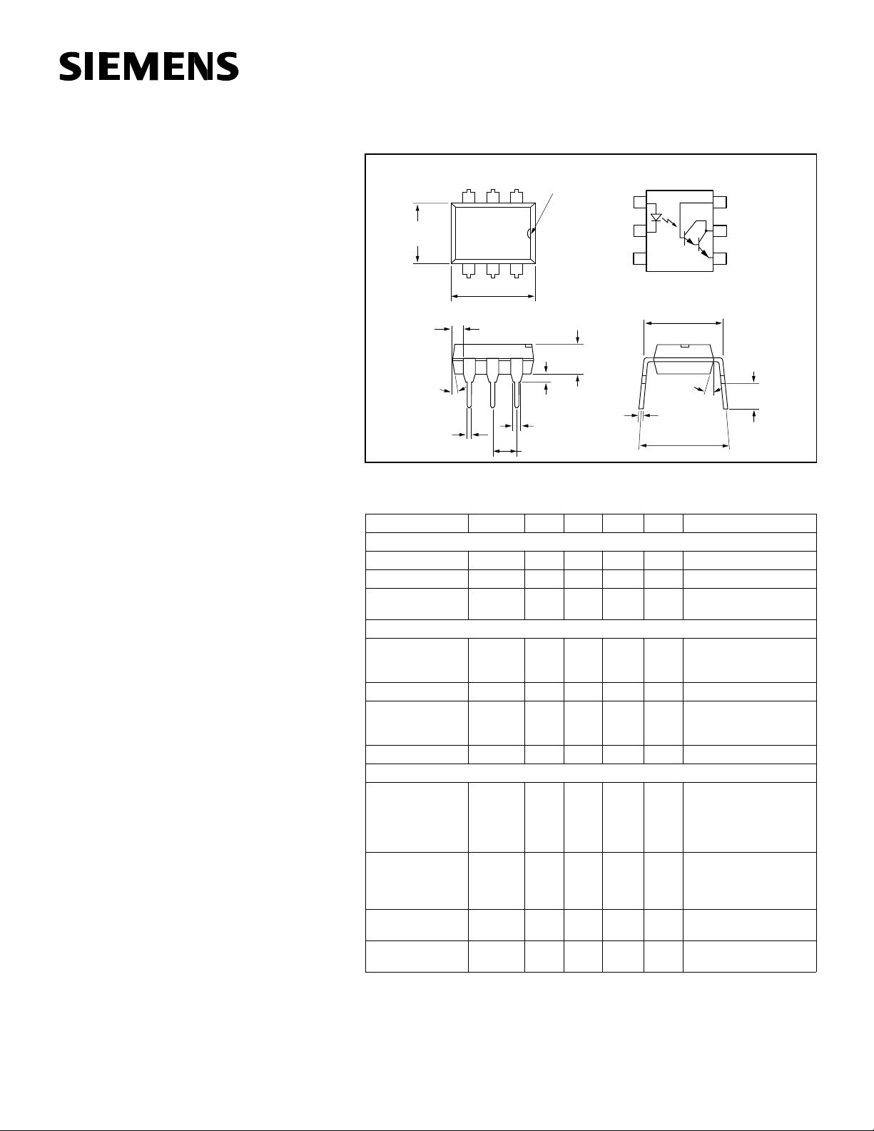
Dimensions in inches (mm)
3
248 (6.30)
256 (6.50)
4
5
.335 (8.50)
.343 (8.70)
.039
(1.00)
min.
4°
typ.
.018 (0.45)
.022 (0.55)
Pin One ID.
12
6
.130 (3.30)
.150 (3.81)
.020 (.051) min.
.031 (0.80)
.035 (0.90)
.100 (2.54) typ.
Anode
Cathode
NC
1
2
3
.300 (7.62)
18° typ.
.010 (.25)
.014 (.35)
.300 (7.62)
.347 (8.82)
typ.
6
Base
5
Collector
4
Emitter
.110 (2.79
.150 (3.81
Emitter
Reverse Voltage.................................................6 V
Continuous Forward Current........................ 60 mA
Power Dissipation at 25 °
Derate Linearly from 25 °
C..........................135 mW
C......................1.8 mW/ ° C
Detector
Collector-Emitter Breakdown Voltage
MCA230/231.................................................30 V
MCA255........................................................55 V
Emitter-Collector Breakdown Voltage ................7 V
Collector-Base Breakdown Voltage
MCA230/231.................................................30 V
MCA255........................................................55 V
Power Dissipation at 25 °
Derate Linearly from 25 °
C..........................210 mW
C......................2.8 mW/ ° C
Package
Total Package Dissipation at 25 ° C
(LED plus Detector)................................260 mW
Derate Linearly from 25 °
Storage Temperature .................. –55 °
Operating Temperature .............. –55 °
Lead Soldering Time at 260 °
C......................3.5 mW/ ° C
C to +150 ° C
C to +100 ° C
C....................10 sec.
Isolation Test V oltage ........................5300 V AC
Isolation Resistance
V
=500 V, T
IO
V
=500 V, T
IO
=25 ° C..................................10
A
=100 ° C................................10
A
Characteristics (T
Emitter
Forward Voltage V
Reverse Current I
Junction
Capacitance
Detector
BV
MCA230/231
MCA255
BV
BV
MCA230/231
MCA55
I
CEO
Package
V
RMS
12
Ω
11
DC Current
Transfer Ratio
MCA230/255
MCA231
Capacitance
Input to Output C
Switching Times t
CEO
ECO
CBO
CEsat
=25 ° C)
A
Symbol Min. Typ. Max. Unit Condition
F
R
C
J
1.1 1.5 V I
50 pF V
30
30
10 µ AV
V
V
7VI
30
55
V
V
100 nA V
0.8
V
1.0
V
1.0
V
1.0
V
1.2
V
CTR
CTR
IO
on
t
off
100
200
0.5 pF
10
35
%
%
µ s
µ s
=50 mA
F
=3 V
R
=3 V
R
I
=100 µ A, I
C
I
=100 µ A, I
C
=10 µ A, I
E
I
=10 µ A, I
C
I
=10 µ A, I
C
=10 V, I
CE
I
=2 mA, I
CE
I
=I
C
F
I
=2 mA, I
C
I
=10 mA, I
C
I
=50 mA, I
C
V
=5 V, I
CE
V
=5 V, I
CE
R
=100 Ω
L
V
=10 V
CE
=50 mA
F
F
F
=0 mA
F
=0 mA
F
=0 mA
F
=0 mA
F
=0 mA
F
=0 mA
F
=16 mA
F
=1 mA
=5 mA
F
=10 mA
F
=10 mA
=1 mA
5–1

C
V
V
V
O
I
Figure 1. Forward voltage versus forward current
1.4
1.3
Ta = -55°C
1.2
1.1
Ta = 25°C
1.0
0.9
Ta = 85°C
0.8
VF - Forward Voltage - V
0.7
100101.1
IF - Forward Current - mA
Figure 2. Normalized non-saturated and saturated
CTRce at T
NCTRc e - Norm alized CTR
= 25 ° C versus LED current
A
1.2
No rma liz ed to:
Vce = 5 V
1.0
IF = 10 mA
0.8
Ta = 25 °C
0.6
0.4
0.2
0.0
.1 1 10 100 1000
IF - LED Curr ent - mA
Vce = 5 V
Vce =1V
Figure 5. Non-saturated and saturated HFE versus base current
10000
8000
6000
4000
2000
HFE - Forward Transfer Gain
Ta = 25°
0
.01 .1 1 10 100
Ib - Base Current - µA
Vce = 5 V
Vce = 1 V
Figure 6. Low to high propagation delay versus
collector load resistance and LED current
80
Ta = 25°C, Vcc = 5
Vth = 1.5 V
60
40
Delay - µs
20
0
tpLH - Low/High Propagation
0 5 10 15 20
IF - LED Current - mA
1KΩ
220Ω
470Ω
100Ω
Figure 3. Normalized non-saturated and saturated
collector-emitter current versus LED current
10
Normalized to:
Ta = 25°C
IF = 10 mA
1
Vce = 5 V
.1
.01
NIce - Normalized Ice
.001
IF - LED Current - mA
Vce = 5 V
Vce = 1V
101.1
100
Figure 4. Normalized collector-base photocurrent
versus LED current
10
Normalized to:
Ta = 25°C
Vcb = 3.5 V
1
IF = 10 mA
.1
.01
NIcb - Normalized Icb
.001
.1 1 10 100
IF - LED Current - mA
Figure 7. High to low propagation delay versus
collector load resistance and LED current
20
15
10
delay - µs
5
0
tpHL - High/Low Propagation
0 5 10 15 20
1KΩ
100Ω
IF - LED Current - mA
Ta = 25°C
Vcc = 5 V
Vth = 1.5 V
Figure 8. Switching timing waveform and schematic
I
F
F=10 KHz,
t
D
t
O
R
t
PLH
VTH=1.5 V
t
PHL
t
t
S
F
DF=50%
F=10 mA
V
CC=
R
5
L
V
5–2
MCA230/231/255
 Loading...