

Siemens HYB3164160T-50, HYB3164160T-60, HYB3165160T-50, HYB3165160T-60 Datasheet
4M x 16-Bit Dynamic RAM
(4k & 8k Refresh)
HYB 3164160T -50/-60
HYB 3165160T -50/-60
Preliminary Information
• 4 194 304 words by 16-bit organization
• 0 to 70 ˚C operating temperature
• Fast access and cycle time
RAS access time:
50 ns (-50 version)
60 ns (-60 version)
Cycle time:
90 ns (-50 version)
110 ns (-60 version)
CAS access time:
13 ns ( -50 version)
15 ns ( -60 version)
• Fast page mode cycle time
35 ns (-50 version)
40 ns (-60 version)
• Single + 3.3 V (± 0.3V) power supply
• Low power dissipation
max. 396 active mW ( HYB 3164160T-50)
max. 360 active mW ( HYB 3164160T-60)
max. 504 active mW ( HYB 3165160T-50)
max. 432 active mW ( HYB 3165160T-60)
7.2 mW standby (TTL)
720 W standby (MOS)
• Read, write, read-modify-write, CAS-before-RAS refresh (CBR),
RAS-only refresh, hidden refresh and self refresh modes
• Fast page mode capability
• 2 CAS / 1 WRITE byte control
• 8192 refresh cycles/128 ms , 13 R/ 9C addresses (HYB 3164160T)
• 4096 refresh cycles/ 64 ms , 12 R/ 10C addresses (HYB 3165160T)
• Plastic Package: P-TSOPII-54-1 500 mil
Semiconductor Group 5
HYB 3164(5)160T-50/-60
4M x 16-DRAM
This device is a 64 MBit dynamic RAM organized 4 194 304 by 16 bits. The device is fabricated in
SIEMENS/IBM most advanced first generation 64Mbit CMOS silicon gate process technology. The
circuit and process design allow this device to achieve high performance and low power dissipation.
This DRAM operates with a single 3.3 +/-0.3V power supply and interfaces with either LVTTL or
LVCMOS levels. Multiplexed address inputs permit the HYB 3164(5)160T to be packaged in a 500
mil wide TSOP-54 plastic package. These packages provide high system bit densities and are
compatible with commonly used automatic testing and insertion equipment.
Ordering Information
Type Ordering
Code
HYB 3164160T-50 on request P-TSOPII-54-1 500 mil DRAM (access time 50 ns)
HYB 3164160T-60 on request P-TSOPII-54-1 500 mil DRAM (access time 60 ns)
HYB 3165160T-50 on request P-TSOPII-54-1 500 mil DRAM (access time 50 ns)
HYB 3165160T-60 on request P-TSOPII-54-1 500 mil DRAM (access time 60 ns)
Pin Names
A0-A12 Address Inputs for HYB 3164160T
A0-A11 Address Inputs for HYB 3165160T
RAS Row Address Strobe
OE Output Enable
I/O1-I/O16 Data Input/Output
UCAS,LCAS Column Address Strobe
WRITE Read/Write Input
Vcc Power Supply ( + 3.3V)
Vss Ground
Package Descriptions
Semiconductor Group 6
P-SOJ-54-1 (500 mil)
P-TSOPII-54-1 (500 mil)
HYB 3164(5)160T-50/-60
4M x 16-DRAM
* Pin 35 is A12 for HYB 3164160T and N.C. for HYB 3165160T
Pin Configuration
Semiconductor Group 7
TRUTH TABLE
HYB 3164(5)160T-50/-60
4M x 16-DRAM
FUNCTION
Standby
Read:Word
Read:Lower Byte
Read:Upper Byte
Write:Word
(Early-Write)
Write:Lower Byte
(Early-Write)
Write:Upper Byte
(Early Write)
Read-ModifyWrite
Fast Page Mode
Read (Word)
Fast Page Mode
Read (Word)
1st
Cycle
2nd
Cycle
RAS LCAS UCASWRITEOE ROW
ADD
COL
ADD
H H - X H - X X X X X
L L H H L ROW COL
L L H H L ROW COL
L H L H L ROW COL
L L L L X ROW COL
L L H L X ROW COL
L H L L X ROW COL
L L L H - L L - H ROW COL
L H - L H - L H L ROW COL
L H - L H - L H L n/a COL
I/O1I/O16
High Impedance
Data Out
Lower Byte:Data Out
Upper-Byte:High-Z
Lower Byte:High-Z
Upper Byte:Data Out
Data In
Lower Byte:Data Out
Upper-Byte:High-Z
Lower Byte:High-Z
Upper Byte:Data Out
Data Out, Data In
Data Out
Data Out
Fast Page Mode
Early Write(Word)
Fast Page Mode
Early Write(Word)
Fast Page Mode
RMW
Fast Page Mode
RMW
RAS only refresh
CAS-before-RAS
refresh
Test Mode Entry
Hidden Refresh
(Read)
Hidden Refresh
(Write)
1st
Cycle
2nd
Cycle
1st
Cycle
2st
Cycle
L H - L H - L L X ROW COL
L H - L H - L L X n/a COL
L H - L H - L H - L L - H ROW COL
L H - L H - L H - L L - H n/a COL
L H H X X ROW n/a
H - L L L H X X n/a
H - L L L L X X n/a
L-H-LL L H L ROW COL
L-H-LL L L X ROW COL
Data In
Data In
Data Out, Data In
Data Out, Data In
High Impedance
High Impedance
High Impedance
Data Out
Data In
Semiconductor Group 8
HYB 3164(5)160T-50/-60
4M x 16-DRAM
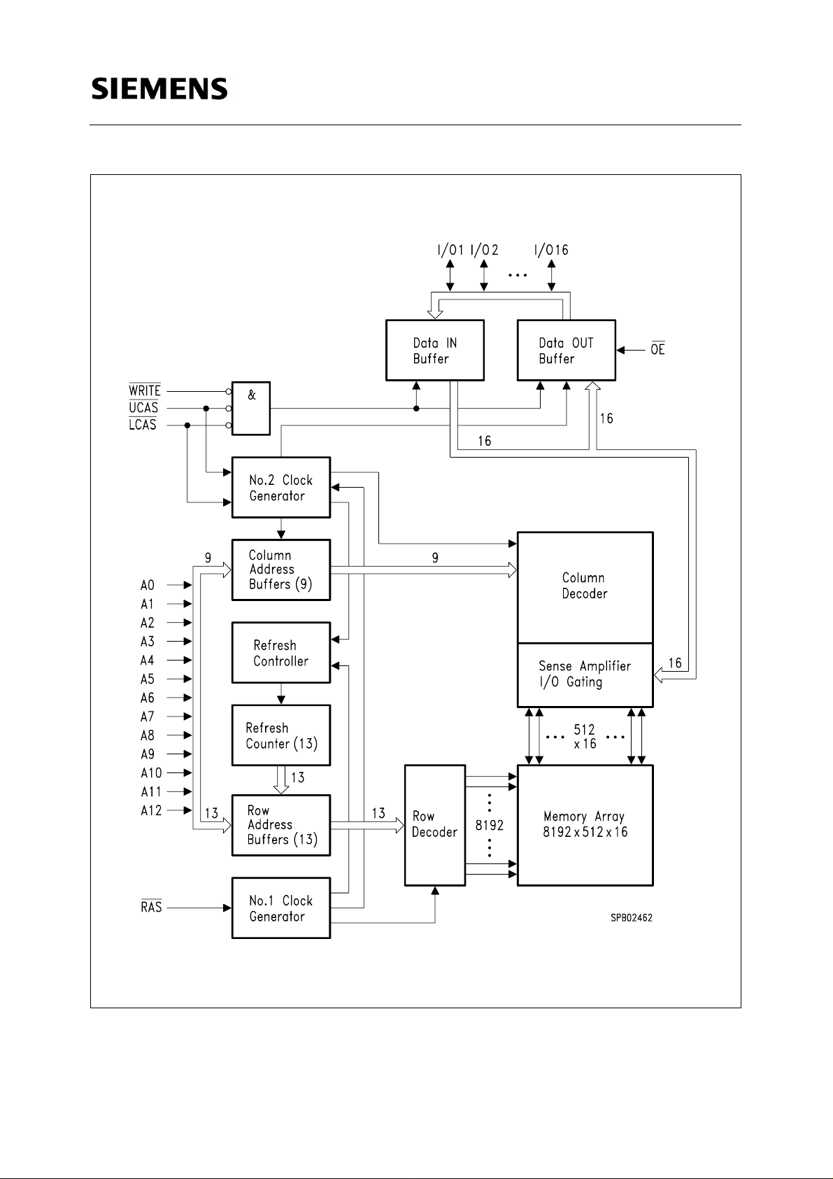
Block Diagram for HYB 3164160T
Semiconductor Group 9
HYB 3164(5)160T-50/-60
4M x 16-DRAM
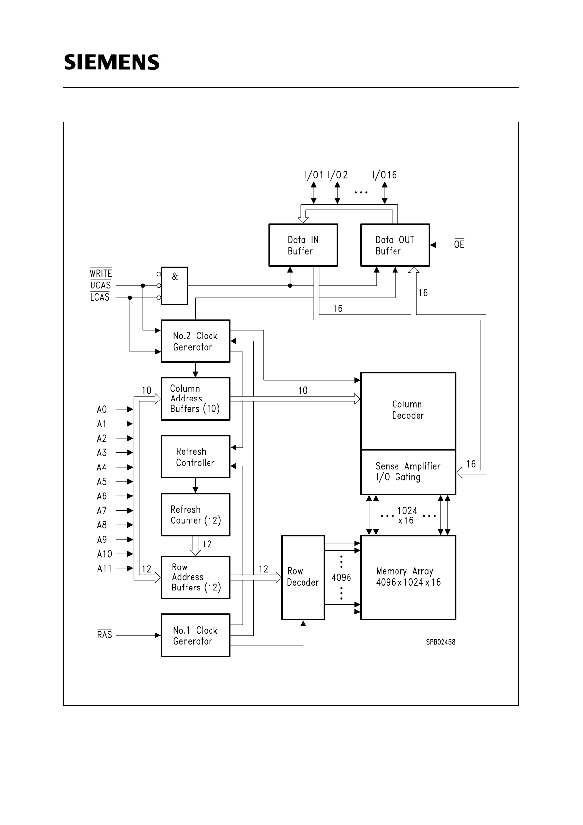
Block Diagram for HYB 3165160T
Semiconductor Group 10
HYB 3164(5)160T-50/-60
4M x 16-DRAM
Absolute Maximum Ratings
Operating temperature range..............................................................................................0 to 70 ˚C
Storage temperature range.........................................................................................– 55 to 150 ˚C
Input/output voltage..................................................................................-0.5 to min (Vcc+0.5,4.6) V
Power supply voltage....................................................................................................-0.5V to 4.6 V
Power dissipation......................................................................................................................1.0 W
Data out current (short circuit)..................................................................................................50 mA
Note
Stresses above those listed under „Absolute Maximum Ratings“ may cause permanent damage of
the device. Exposure to absolute maximum rating conditions for extended periods may effect device
reliability.
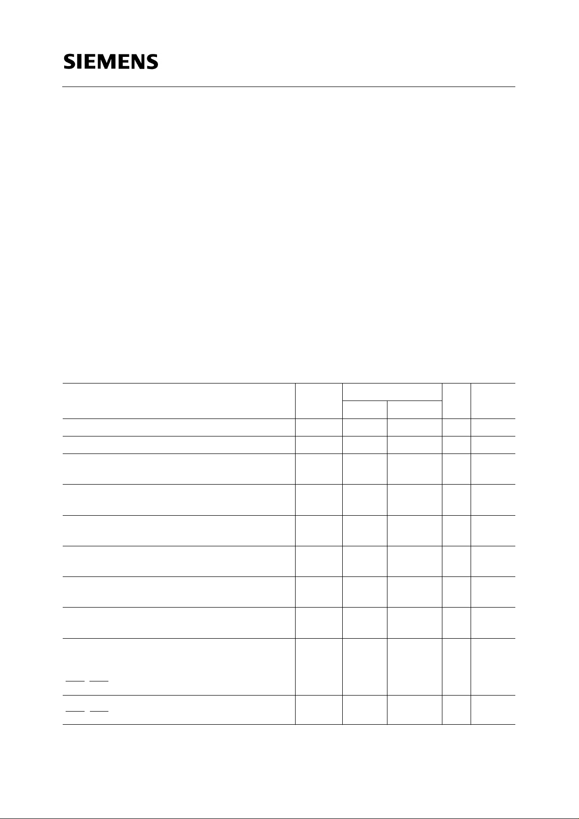
DC Characteristics
T
= 0 to 70 ˚C,
A
V
= 0 V,
SS
V
= 3.3 V ± 0.3 V, (values in brackets for HYB 3165160T)
CC
Parameter Symbol Limit Values Unit Note
min. max.
Input high voltage
Input low voltage
Output high voltage (LVTTL)
V
V
V
IH
IL
OH
2.0 Vcc+0.3 V 1)
– 0.3 0.8 V 1)
2.4 – V
Output „H“ level voltage (Iout = -2mA)
Output low voltage (LVTTL)
V
OL
– 0.4 V
Output „L“level voltage (Iout = +2mA)
Output high voltage (LVCMOS)
V
OH
Vcc-0.2 - V
Output „H“ level voltage (Iout = -100uA)
Ouput low voltage (LVCMOS)
V
OL
- 0.2 V
Output „L“ level voltage (Iout = +100uA)
Input leakage current,any input
(0 V <Vin < Vcc , all other pins = 0 V
Output leakage current
(DO is disabled, 0 V <
Vout
< Vcc )
I
I
I(L)
O(L)
– 2 2 µA
– 2 2 µA
Average
Vcc
supply current:
-50 ns version
-60 ns version
(RAS, CAS, address cycling: tRC = tRC min.)
Standby Vcc supply current
(RAS=CAS=Vih)
Semiconductor Group 11
I
I
CC1
CC2
–
–
110 (140)
100 (120)mAmA
– 2 mA –
2) 3) 4)
HYB 3164(5)160T-50/-60
4M x 16-DRAM
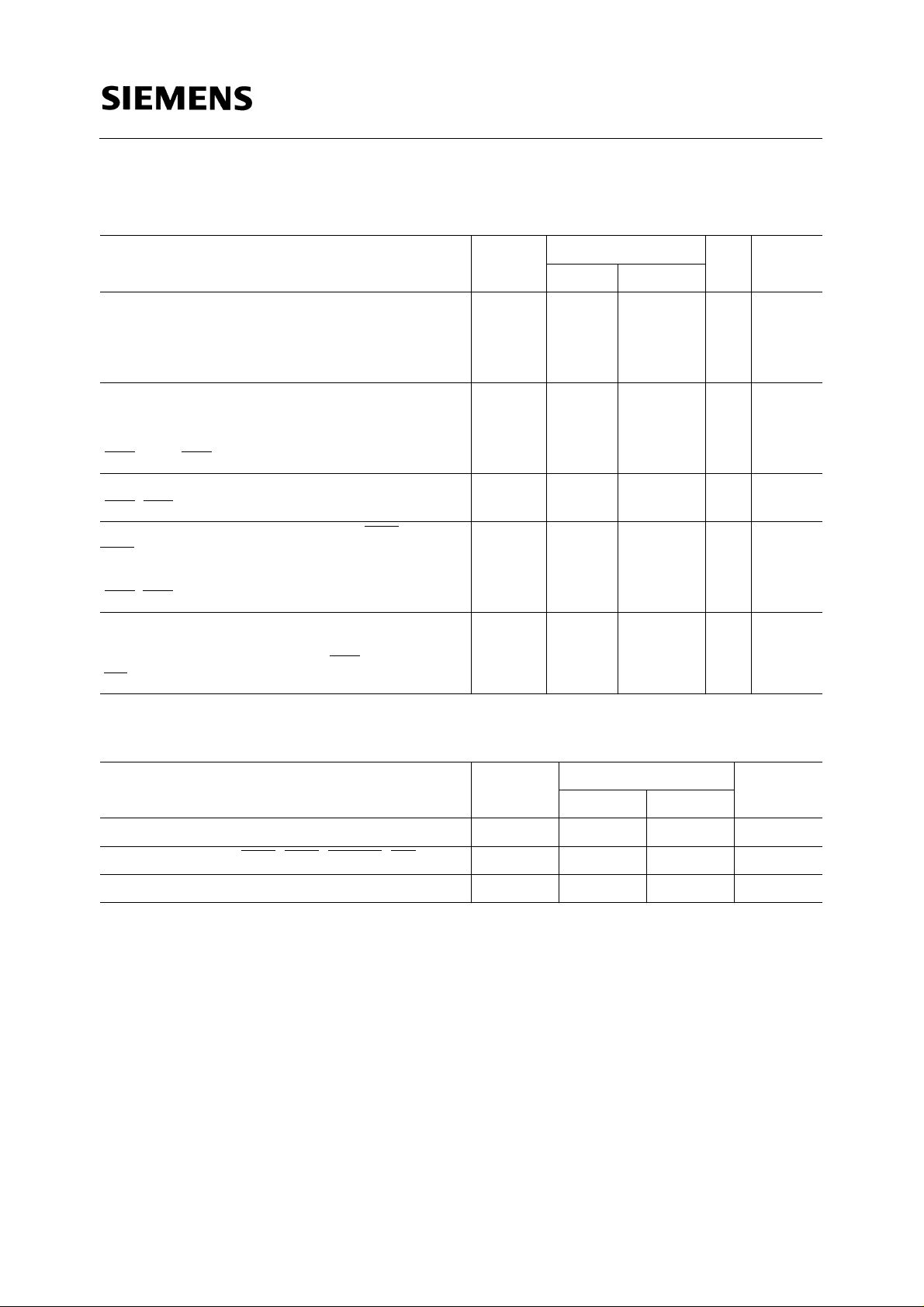
DC Characteristics
T
= 0 to 70 ˚C,
A
V
= 0 V,
SS
(cont’d)
V
= 3.3 V ± 0.3 V, (values in brackets for HYB 3165160T)
CC
Parameter Symbol Limit Values Unit Note
min. max.
AverageVcc supply current, during RAS-only
refresh cycles: -50 ns version
-60 ns version
(RAS cycling: CAS =VIH: tRC = tRC min.)
AverageVcc supply current,
during fast page mode: -50 ns version
-60 ns version
(RAS =
V
, CAS, address cycling: tPC=tPC min.)
IL
Standby Vcc supply current
(RAS=CAS=Vcc-0.2V)
Average Vcc supply current, during
CAS-before-
RAS refresh mode: -50 ns version
-60 ns version
(RAS, CAS cycling: tRC = tRC min.)
Self Refresh Current
Average Power Supply Current during Self Refresh.
(CBR cycle with tRAS>TRASSmin,
WE = Vcc-0.2V, Address and Din=Vcc-0.2V or 0.2V)
CAS held low,
I
I
I
I
I
CC3
CC4
CC5
CC6
CC7
–
–
–
–
110 (140)
100 (120)mAmA
85 (85)
75 (75)mAmA
– 200 A –
–
–
110 (140)
100 (120)mAmA
– 400 A
2) 4)
2) 3) 4)
2) 4)
Capacitance
T
= 0 to 70 ˚C,
A
V
= 3.3 V ± 0.3V,f = 1 MHz
CC
Parameter Symbol Limit Values Unit
min. max.
Input capacitance (A0 to A11,A12)
Input capacitance (
RAS, CAS, WRITE, OE)
I/O capacitance (I/O1-I/O16)
C
C
C
I1
I2
IO
–5pF
–7pF
–7pF
Semiconductor Group 12
 Loading...