

Siemens HYB3117800BSJ-50, HYB3117800BSJ-60 Datasheet
2M × 8 - Bit Dynamic RAM
2k Refresh
(Fast Page Mode)
Advanced Information
• 2 097 152 words by 8-bit organization
• 0 to 70 °C operating temperature
• Fast Page Mode operation
• Performance:
HYB 5117800/BSJ-50/-60
HYB 3117800BSJ-50/-60
-50 -60
t
RAC
t
CAC
t
AA
t
RC
t
PC
• Power dissipation:
Power Supply 5 ± 10% 3.3 ± 0.3 V
Active 440 385 288 252 mW
TTL Standby 11 7.2 mW
CMOS Standby 5.5 3.6 mW
• Read, write, read-modify-write, CAS-before-RAS refresh, RAS-only refresh, hidden refresh
and test mode
RAS access time 50 60 ns
CAS access time 13 15 ns
Access time from address 25 30 ns
Read/Write cycle time 84 104 ns
Fast page mode cycle time 35 40 ns
HYB5117800 HYB3117800
-50 -60 -50 -60
• All inputs, outputs and clocks fully TTL (5 V versions) and LV-TTL (3.3 V version)-compatible
• 2048 refresh cycles / 32 ms (2k-refresh)
• Plastic Package: P-SOJ-28-3 400 mil
Semiconductor Group 1 1998-10-01
HYB 5(3)117800/BSJ-50/-60
2M × 8 DRAM
The HYB 5(3)117800 are 16 MBit dynamic RAMs based on the die revisions “G” & “F” and
organized as 2 097 152 words by 8-bits. The HYB 5(3)117800 utilizes a submicron CMOS silicon
gate process technology, as well as advanced circuit techniques to provide wide operating margins,
both internally and for the system user. Multiplexed address inputs permit the HYB 5(3)117800 to
be packaged in a standard SOJ-28 plastic package. Package with 400 mil width are available.
These packages provide high system bit densities and are compatible with commonly used
automatic testing and insertion equipment.
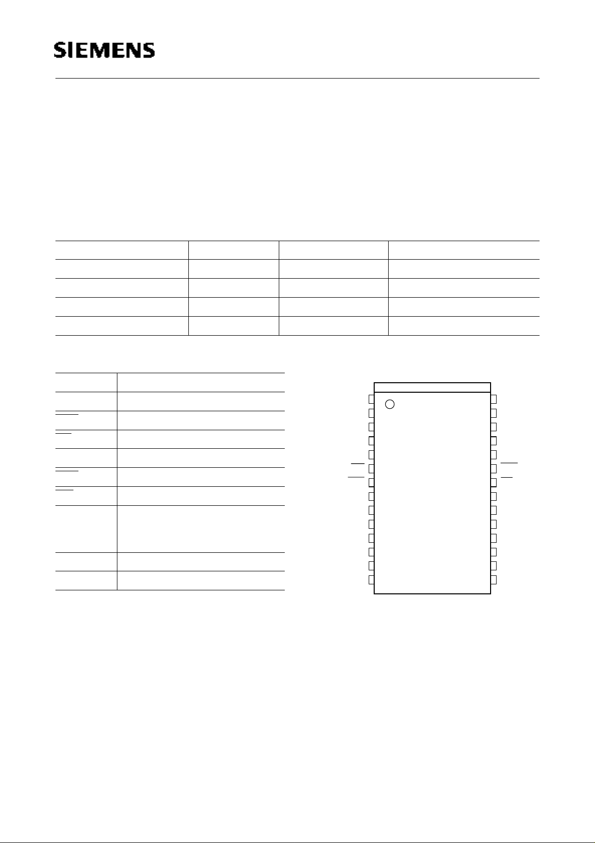
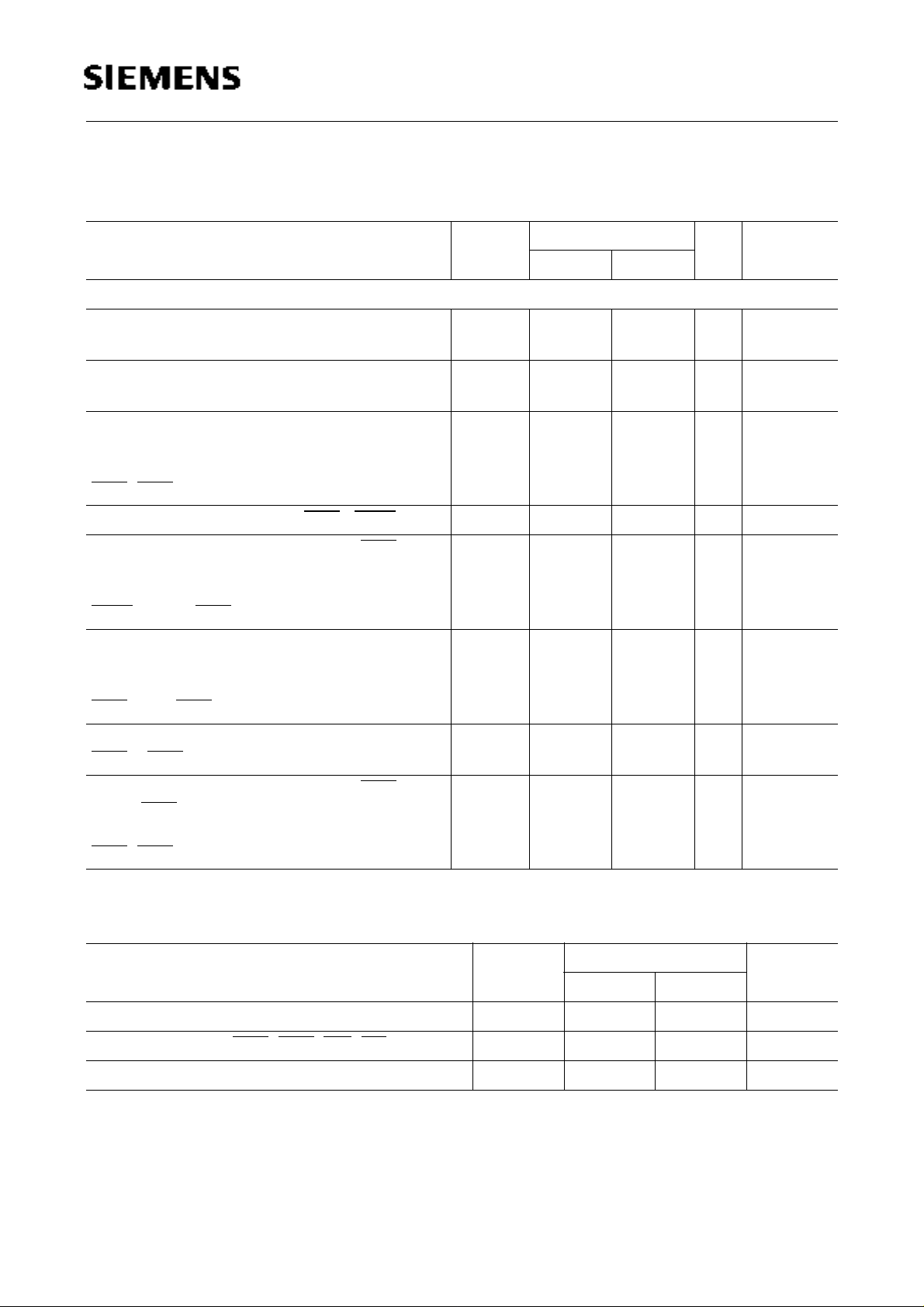
Ordering Information
Type Ordering Code Package Descriptions
HYB 5117800BSJ-50 Q67100-Q1092 P-SOJ-28-3 400 mil 5 V 50 ns FPM-DRAM
HYB 5117800BSJ-60 Q67100-Q1093 P-SOJ-28-3 400 mil 5 V 60 ns FPM-DRAM
HYB 3117800BSJ-50 on request P-SOJ-28-3 400 mil 3.3 V 50 ns FPM-DRAM
HYB 3117800BSJ-60 on request P-SOJ-28-3 400 mil 3.3 V 60 ns FPM-DRAM
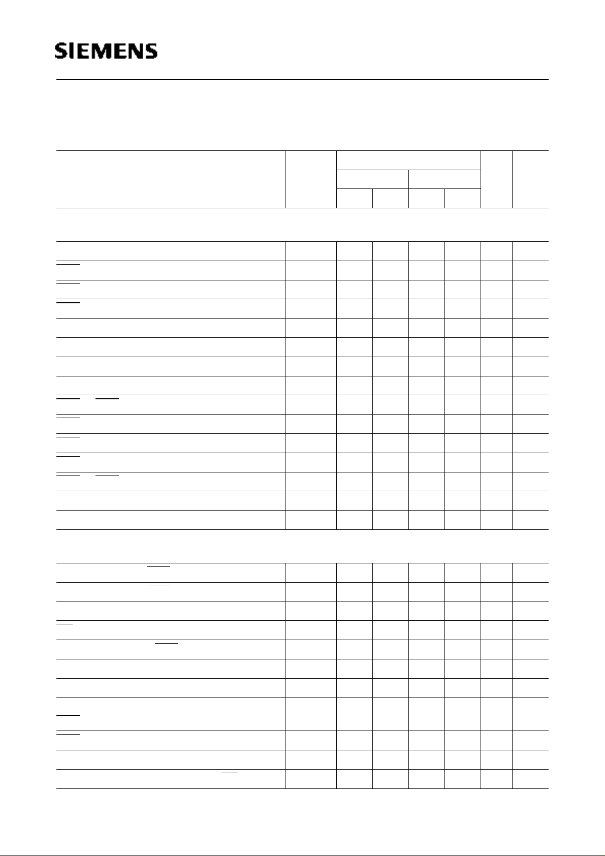
Pin Names and Configuration
A0 - A10 Row Address Inputs
A0 - A9 Column Address Inputs
RAS Row Address Strobe
OE Output Enable
I/O1 - I/O8 Data Input/Output
CAS Column Address Strobe
WE Read/Write Input
V
CC
Power Supply
+ 5 V for HYB 5117800
+ 3.3 V for HYB 3117800
V
SS
Ground (0 V)
N.C. Not Connected
V
CC
I/O1
I/O2
I/O3
I/O4
WE
RAS
N.C.
A10
A0
A1
A2
A3
V
CC
P-SOJ-28 400 mil
1
2
3
4
5
6
7
8
9
10
11
12
13
14 15
28
27
26
25
24
23
22
21
20
19
18
17
16
V
SS
I/O8
I/O7
I/O6
I/O5
CAS
OE
A9
A8
A7
A6
A5
A4
V
SS
SPP02803
Semiconductor Group 2 1998-10-01
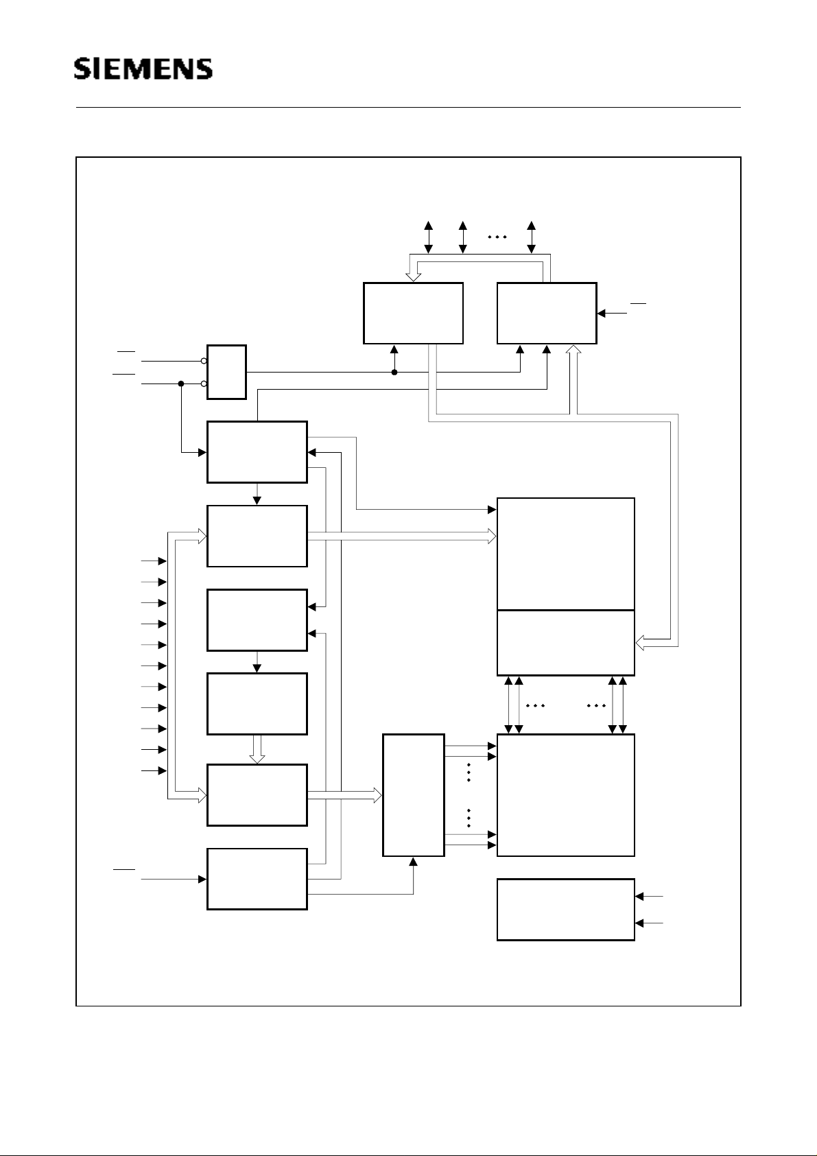
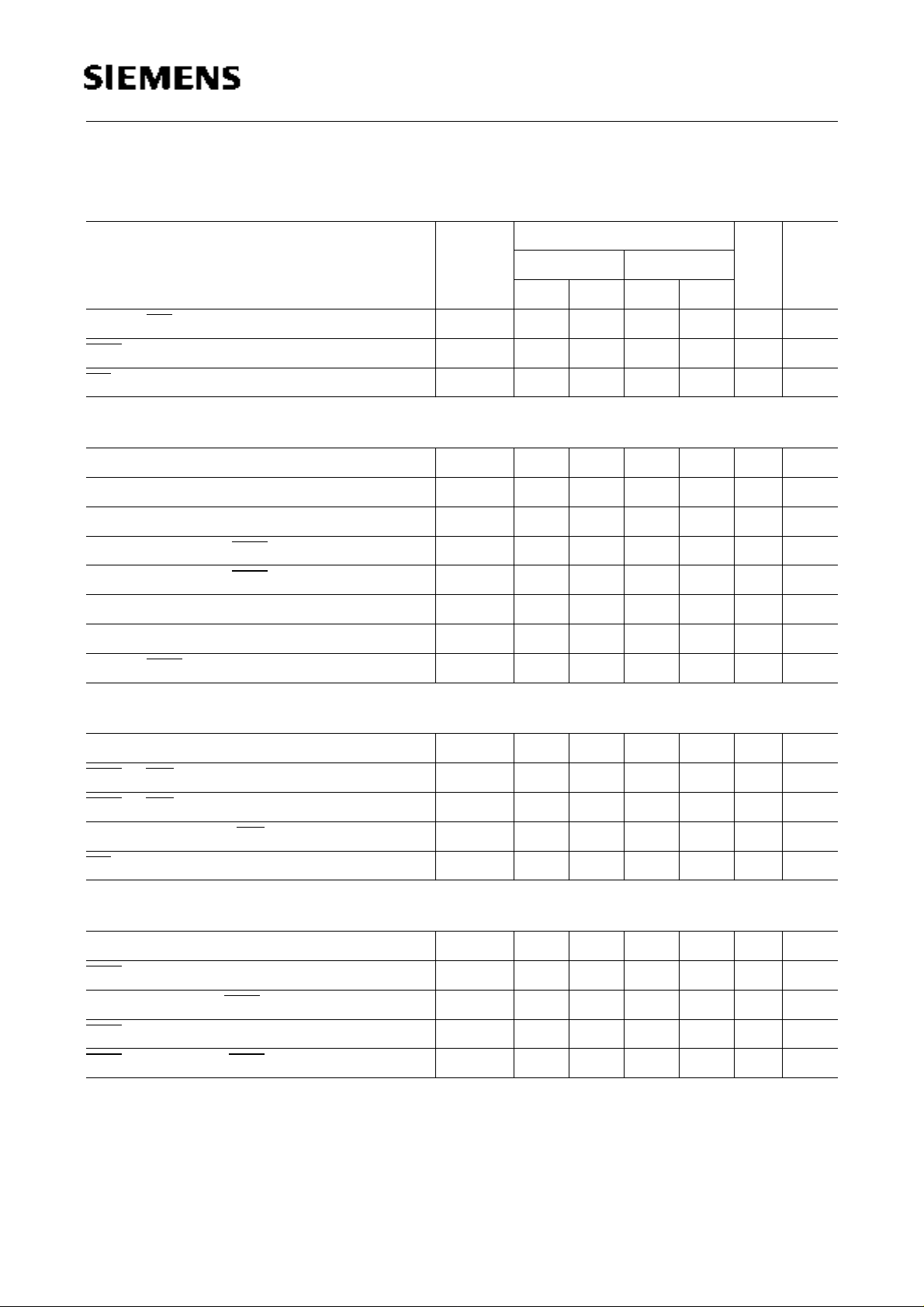
I/O1
HYB 5(3)117800/BSJ-50/-60
2M × 8 DRAM
I/O2
I/O8
WE
CAS
A0
A1
A2
A3
A4
A5
A6
A7
A8
A9
A10
10
11
&
No.2 Clock
Generator
Column
Address
Buffers (10)
Refresh
Controller
Refresh
Counter (11)
11
Row
Address
Buffers (11)
11
Data IN
Buffer
10
Row
Decoder
8
2048
Data OUT
Buffer
8
Column
Decoder
Sense Amplifier
I/O Gating
1024
x 8
Memory Array
2048 x 1024 x 8
OE
4
RAS
No.1 Clock
Generator
Voltage Down
Generator
SPB03456
V
CC
V
CC
(internal)
Block Diagram
Semiconductor Group 3 1998-10-01
HYB 5(3)117800/BSJ-50/-60
2M × 8 DRAM
Absolute Maximum Ratings
Operating temperature range ........................................................................................... 0 to 70 °C
Storage temperature range........................................................................................ – 55 to 150 °C
Input/output voltage (5 V versions)................................................... – 0.5 to min (VCC+ 0.5, 7.0) V
Input/output voltage (3.3 V versions)................................................ – 0.5 to min (VCC+ 0.5, 4.6) V
Power supply voltage (5 V versions) ....................................................................... – 1.0 V to 7.0 V
Power supply voltage (3.3 V versions) .................................................................... – 1.0 V to 4.6 V
Power dissipation (5 V versions) .............................................................................................1.0 W
Power dissipation (3.3 V versions) ..........................................................................................0.5 W
Data out current (short circuit) ................................................................................................50 mA
Note: Stresses above those listed under “Absolute Maximum Ratings” may cause permanent
damage of the device. Exposure to absolute maximum rating conditions for extended periods
may affect device reliability.
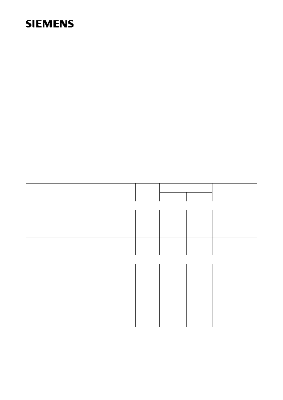
DC Characteristics
T
= 0 to 70 °C, VSS = 0 V, tT = 2 ns
A
Parameter Symbol Limit Values Unit Test
min. max.
Condition
5 V Versions
Power supply voltage V
Input high voltage V
Input low voltage V
Output high voltage (I
Output low voltage (I
= – 5 mA) V
OUT
= 4.2 mA) V
OUT
CC
IH
IL
OH
OL
4.5 5.5 V
2.4 VCC+ 0.5 V
– 0.5 0.8 V
2.4 – V
– 0.4 V
1
1
1
1
3.3 V Versions
Power supply voltage V
Input high voltage V
Input low voltage V
TTL Output high voltage (I
TTL Output low voltage (I
CMOS Output high voltage (I
CMOS Output low voltage (I
= – 2 mA) V
OUT
= 2 mA) V
OUT
= – 100 µA) V
OUT
= 100 µA) V
OUT
CC
IH
IL
OH
OL
OH
OL
3.0 3.6 V
2.0 VCC+ 0.5 V
– 0.5 0.8 V
2.4 – V
– 0.4 V
V
– 0.2 – V
CC
– 0.2 V
1
1
1
1
Semiconductor Group 4 1998-10-01
HYB 5(3)117800/BSJ-50/-60
2M × 8 DRAM
DC Characteristics (cont’d)
T
= 0 to 70 °C, VSS = 0 V, tT = 2 ns
A
Parameter Symbol Limit Values Unit Test
Condition
1
1
2, 3, 4
2, 3, 4
2, 4
2, 4
2, 3,) 4
2, 3, 4
1
Common Parameters
Input leakage current
(0 V ≤ VIH≤ VCC + 0.3 V, all other pins = 0 V)
Output leakage current
(DO is disabled, 0 V ≤ V
≤ VCC + 0.3 V)
OUT
Average VCC supply current
-50 ns version
-60 ns version
(RAS, CAS, address cycling: tRC = t
RC MIN.
)
Standby VCC supply current (RAS = CAS = VIH) I
Average VCC supply current, during RAS-only
refresh cycles -50 ns version
-60 ns version
(RAS cycling, CAS = VIH, tRC = t
RC MIN.
)
Average VCC supply current,
during fast page mode -50 ns version
-60 ns version
(RAS = VIL, CAS, address cycling: tPC = t
PC MIN.
)
Standby VCC supply current
(RAS = CAS = VCC – 0.2 V)
I
I
I
I
I
I
I(L)
O(L)
CC1
CC2
CC3
CC4
CC5
min. max.
– 10 10 µA
– 10 10 µA
–
–
80
70
mA
mA
–2mA–
–
–
–
–
80
70
25
20
mA
mA
mA
mA
–1mA
Average VCC supply current, during CASbefore-RAS refresh mode -50 ns version
-60 ns version
(RAS, CAS cycling: tRC = t
RC MIN.
)
I
CC6
–
–
80
70
mA
mA
2, 4
2,) 4
Capacitance
T
= 0 to 70 °C,VCC = 5 V ± 10 %, f = 1 MHz
A
Parameter Symbol Limit Values Unit
min. max.
Input capacitance (A0 to A10) C
Input capacitance (RAS, CAS, WE, OE) C
I/O capacitance (I/O1 to I/O8) C
I1
I2
IO
–5pF
–7pF
–7pF
Semiconductor Group 5 1998-10-01
HYB 5(3)117800/BSJ-50/-60
2M × 8 DRAM
AC Characteristics
T
= 0 to 70 °C, VCC = 5 V ± 10 % / VCC = 3.3 V ± 0.3 V, tT = 5 ns
A
5, 6
Parameter Symbol Limit Values Unit Note
-50 -60
min. max. min. max.
Common Parameters
Random read or write cycle time t
RAS precharge time t
RAS pulse width t
CAS pulse width t
Row address setup time t
Row address hold time t
Column address setup time t
Column address hold time t
RAS to CAS delay time t
RAS to column address delay time t
RAS hold time t
CAS hold time t
CAS to RAS precharge time t
Transition time (rise and fall) t
Refresh period t
RC
RP
RAS
CAS
ASR
RAH
ASC
CAH
RCD
RAD
RSH
CSH
CRP
T
REF
90 – 110 – ns
30 – 40 – ns
50 10k 60 10k ns
13 10k 15 10k ns
0–0–ns
8 – 10 – ns
0–0–ns
10 – 15 – ns
18 37 20 45
13 25 15 30 ns
13 15 – ns
50 60 – ns
5–5–ns
3 50 3 50 ns
7
– 32 – 32 ms
Read Cycle
Access time from RAS t
Access time from CAS t
Access time from column address t
OE access time t
Column address to RAS lead time t
Read command setup time t
Read command hold time t
Read command hold time referenced to
RAC
CAC
AA
OEA
RAL
RCS
RCH
t
RRH
– 50 – 60 ns
– 13 – 15 ns
– 25 – 30 ns
– 13 – 15 ns
25 – 30 – ns
0–0–ns
0–0–ns
0–0–ns
8, 9
8, 9
8, 10
11
11
RAS
CAS to output in low-Z t
Output buffer turn-off delay t
Output buffer turn-off delay from OE t
CLZ
OFF
OEZ
0–0–ns
0 13 0 15 ns
0 13 0 15 ns
8
12
12
Semiconductor Group 6 1998-10-01
HYB 5(3)117800/BSJ-50/-60
2M × 8 DRAM
AC Characteristics (cont’d)
T
= 0 to 70 °C, VCC = 5 V ± 10 % / VCC = 3.3 V ± 0.3 V, tT = 5 ns
A
5, 6
Parameter Symbol Limit Values Unit Note
-50 -60
min. max. min. max.
Data to OE low delay t
CAS high to data delay t
OE high to data delay t
DZO
CDD
ODD
0–0–ns
13 – 15 – ns
13 – 15 – ns
13
14
14
Write Cycle
Write command hold time t
Write command pulse width t
Write command setup time t
Write command to RAS lead time t
Write command to CAS lead time t
Data setup time t
Data hold time t
Data to CAS low delay t
WCH
WP
WCS
RWL
CWL
DS
DH
DZC
8 – 10 – ns
8 – 10 – ns
0–0–ns
15
13 – 15 – ns
13 – 15 – ns
0–0–ns
10 – 10 – ns
0–0–ns
16
16
13
Read-Modify-Write Cycle
Read-write cycle time t
RAS to WE delay time t
CAS to WE delay time t
Column address to WE delay time t
OE command hold time t
Fast Page Mode Cycle
Fast page mode cycle time t
CAS precharge time t
Access time from CAS precharge t
RAS pulse width t
CAS precharge to RAS Delay t
RWC
RWD
CWD
AWD
OEH
PC
CP
CPA
RAS
RHPC
126 – 150 – ns
68 – 80 – ns
31 – 35 – ns
43 – 50 – ns
13 – 15 – ns
35 – 40 – ns
10 – 10 – ns
– 30 – 35 ns
50 200k 60 200k ns
30 – 35 – ns
15
15
15
7
Semiconductor Group 7 1998-10-01
 Loading...