

Page 1
Company Confidential s Com
Copyright 2005© Siemens AG
Service Repair Documentation
Level 2.5e – A70, A75
Release Date Department Notes to change
1.0 06.06.2005 ICM MP CCQ GRM T New document
Page 1 of 53
TD_Repair_L2.5_A70_A75_R1.0.pdf Release 1.0
Page 2

Company Confidential s Com
Copyright 2005© Siemens AG
Table of Contents:
1 Instruction 4
2 List of available level 2,5e parts A70 5
3 List of available level 2,5e parts A75 6
4 Required Equipment for Level 2,5e 8
5 Required Software for Level 2,5e 8
6 Radio Part 9
6.1 BLOCK DIAGRAM RF PART 10
6.2 POWER SUPPLY RF-PART 11
6.3 FREQUENCY GENERATION 11
6.4 RECEIVER 15
6.5 TRANSMITTER 16
6.6 BRIGHT IC OVERVIEW 17
6.7 ANTENNA SWITCH (ELECTRICAL/MECHANICAL) 19
7 Logic / Control 22
7.1 OVERVIEW OF HARDWARE STRUCTURE A70 22
7.2 OVERVIEW OF HARDWARE STRUCTURE A75 23
7.3 EGOLDLITE 24
7.4 SRAM 30
7.5 FLASH 30
7.6 SIM 30
7.7 VIBRATION MOTOR 30
7.8 DISPLAY MODULES 31
7.9 ILLUMINATION – KEYBOARD 33
8 Acoustic 34
9 Power Supply, Battery and Charging 34
9.1 POWER SUPPLY ASIC 35
9.2 BATTERY 42
9.3 CHARGING CONCEPT 43
Page 2 of 53
TD_Repair_L2.5_A70_A75_R1.0.pdf Release 1.0
Page 3

Company Confidential s Com
Copyright 2005© Siemens AG
10 Interfaces 46
10.1 VIBRA (XG220) 46
10.2 EARPIECE (XG243) 47
10.3 MICROPHONE 48
10.4 BATTERY (X181) 48
10.5 IO CONNECTOR (X211) WITH ESD PROTECTION (Z211) 49
10.6 SIM 51
11 Keyboard 52
Page 3 of 53
TD_Repair_L2.5_A70_A75_R1.0.pdf Release 1.0
Page 4

Company Confidential s Com
Copyright 2005© Siemens AG
1 Instruction
This Service Repair Documentation is intended to carry out repairs on Siemens repair level
2.5. The described failures shall be repaired in Siemens authorized local workshops only.
All repairs have to be carried out in an ESD protected environment and with ESD protected
equipment/tools. For all activities the international ESD regulations have to be considered.
Assembling/disassembling has to be done according to the latest A70, A75 Level 2 repair
documentation. It has to be ensured that every repaired mobile Phone is checked according
to the latest released General Test Instruction document (both documents are available in the
Technical Support section of the C-market).
Check at least weekly C-market for updates and consider all A70, A75 related Customer
Care Information, and Repair Information who are relevant for A70, A75.
A70 Partnumber on IMEI label: S30880-S2770-#xxx
A75 Partnumber on IMEI label: S30880-S2790-#xxx
, while # may be any letter (A-Z) and xxx may be any number from 100, 101, 102....
Scrap Handling: All Scrap information given in this manual are related to the
SCRAP-Rules and instructions.
Attention: Consider the new "LEAD-FREE" soldering rules (A70 and A75 affected)
(available in the communication market), avoid excessive heat.
If you have any questions regarding the repair procedures or technical questions spare not
hesitate to contact our technical support team in Kamp-Lintfort, Germany:
Tel.: +49 2842 95 4666
Fax: +49 2842 95 4302
e-mail: st-support@klf.siemens.de
Page 4 of 53
TD_Repair_L2.5_A70_A75_R1.0.pdf Release 1.0
Page 5

Company Confidential s Com
Copyright 2005© Siemens AG
2 List of available level 2,5e parts A70
(according to Component Matrix V1.03 - check C-market for updates)
RF
Product
A70 HIT C204 L36377-F6225-M CAPACITOR 2U2 (Cap-Type4)
A70 HIT C230 L36377-F6225-M CAPACITOR 2U2 (Cap-Type4)
A70 HIT C368 L36377-F6225-M CAPACITOR 2U2 (Cap-Type4)
A70 HIT C369 L36377-F6225-M CAPACITOR 2U2 (Cap-Type4)
A70 HIT C370 L36377-F6225-M CAPACITOR 2U2 (Cap-Type4)
A70 HIT C371 L36377-F6225-M CAPACITOR 2U2 (Cap-Type4)
A70 HIT C372 L36377-F6105-K CAPACITOR 1U (Cap-Type6)
A70 HIT C373 L36377-F6225-M CAPACITOR 2U2 (Cap-Type4)
A70 HIT C377 L36377-F6225-M CAPACITOR 2U2 (Cap-Type4)
A70 HIT C916 L36377-F6225-M CAPACITOR 2U2 (Cap-Type4)
A70 HIT D171 L50610-L6150-D670 IC EGOLDLITE PMB7860
A70 HIT D361 L50645-J4682-Y55 IC ASIC SALZBURG75 TWIGO3+75
A70 HIT D901 L50651-Z2002-A82 IC MODUL PA PF0814 (PA-Type2)
A70 HIT D902 L50645-K280-Y303 IC FEM HITACHI GSM900 1800 1900 (Fem-Type5)
A70 HIT D903 L50620-L6170-D670 IC TRANCEIVER HD155165BP PB Free
A70 HIT N308 L50610-C6153-D670 IC V-REG 2.9V (Vr-Type2) PB Free
A70 HIT R106 L36852-C-X RESISTOR 0R0 (Res-Type8)
A70 HIT R141 L36852-C-X RESISTOR 0R0 (Res-Type8)
A70 HIT R201 L36852-C-X RESISTOR 0R0 (Res-Type8)
A70 HIT R204 L36852-C-X RESISTOR 0R0 (Res-Type8)
A70 HIT R205 L36852-C-X RESISTOR 0R0 (Res-Type8)
A70 HIT R221 L36852-C-X RESISTOR 0R0 (Res-Type8)
A70 HIT R222 L36852-C-X RESISTOR 0R0 (Res-Type8)
A70 HIT R295 L36852-C-X RESISTOR 0R0 (Res-Type8)
A70 HIT R371 L36852-C-X RESISTOR 0R0 (Res-Type8)
A70 HIT R805 L36852-C-X RESISTOR 0R0 (Res-Type8)
A70 HIT R902 L36852-C-X RESISTOR 0R0 (Res-Type8)
A70 HIT R955 L36120-F4223-H RESISTOR TEMP 22K (Res-Type7)
A70 HIT R958 L36852-C-X RESISTOR 0R0 (Res-Type8)
A70 HIT V151 L36840-D5062-D670 DIODE RB751S (Di-Type3)
A70 HIT V211 L36830-C1097-D670 TRANSISTOR FDG313N (Tra-Type1)
A70 HIT V222 L36830-C1112-D670 TRANSISTOR SI1902 (Tra-Type4)
A70 HIT V361 L36830-C1110-D670 TRANSISTOR SI3911 (Tra-Type3)
A70 HIT Z171 L50645-F102-Y40 QUARZ 32,768KHZ (Q-Type4)
A70 HIT Z211 L50640-U6034-D670 FILTER EMI (Fi-Type3) PB Free
A70 HIT Z950 L36145-F260-Y17 QUARZ 26MHZ (Q-Type4)
Chipset
ID Order Number Description CM
Page 5 of 53
TD_Repair_L2.5_A70_A75_R1.0.pdf Release 1.0
Page 6

Company Confidential s Com
Copyright 2005© Siemens AG
3 List of available level 2,5e parts A75
(according to Component Matrix V1.03 - check C-market for updates)
RF
Product
A75 HIT C165 L36853-C9104-M4 CAPACITOR 100N (Cap-Type2)
A75 HIT C200 L36853-C9104-M4 CAPACITOR 100N (Cap-Type2)
A75 HIT C204 L36377-F6225-M CAPACITOR 2U2 (Cap-Type4)
A75 HIT C209 L36853-C9104-M4 CAPACITOR 100N (Cap-Type2)
A75 HIT C220 L36853-C9104-M4 CAPACITOR 100N (Cap-Type2)
A75 HIT C229 L36853-C9104-M4 CAPACITOR 100N (Cap-Type2)
A75 HIT C230 L36377-F6225-M CAPACITOR 2U2 (Cap-Type4)
A75 HIT C236 L36853-C9104-M4 CAPACITOR 100N (Cap-Type2)
A75 HIT C283 L36377-F6105-K CAPACITOR 1U (Cap-Type6)
A75 HIT C284 L36377-F6105-K CAPACITOR 1U (Cap-Type6)
A75 HIT C285 L36377-F6105-K CAPACITOR 1U (Cap-Type6)
A75 HIT C286 L36377-F6105-K CAPACITOR 1U (Cap-Type6)
A75 HIT C287 L36377-F6225-M CAPACITOR 2U2 (Cap-Type4)
A75 HIT C288 L36377-F6225-M CAPACITOR 2U2 (Cap-Type4)
A75 HIT C289 L36377-F6225-M CAPACITOR 2U2 (Cap-Type4)
A75 HIT C362 L36853-C9104-M4 CAPACITOR 100N (Cap-Type2)
A75 HIT C363 L36853-C9104-M4 CAPACITOR 100N (Cap-Type2)
A75 HIT C364 L36853-C9104-M4 CAPACITOR 100N (Cap-Type2)
A75 HIT C365 L36853-C9104-M4 CAPACITOR 100N (Cap-Type2)
A75 HIT C366 L36853-C9104-M4 CAPACITOR 100N (Cap-Type2)
A75 HIT C367 L36853-C9104-M4 CAPACITOR 100N (Cap-Type2)
A75 HIT C369 L36377-F6225-M CAPACITOR 2U2 (Cap-Type4)
A75 HIT C370 L36377-F6225-M CAPACITOR 2U2 (Cap-Type4)
A75 HIT C371 L36377-F6225-M CAPACITOR 2U2 (Cap-Type4)
A75 HIT C372 L36377-F6105-K CAPACITOR 1U (Cap-Type6)
A75 HIT C373 L36377-F6225-M CAPACITOR 2U2 (Cap-Type4)
A75 HIT C374 L36853-C9104-M4 CAPACITOR 100N (Cap-Type2)
A75 HIT C377 L36377-F6225-M CAPACITOR 2U2 (Cap-Type4)
A75 HIT C381 L36853-C9104-M4 CAPACITOR 100N (Cap-Type2)
A75 HIT C382 L36853-C9104-M4 CAPACITOR 100N (Cap-Type2)
A75 HIT C383 L36853-C9104-M4 CAPACITOR 100N (Cap-Type2)
A75 HIT C384 L36853-C9104-M4 CAPACITOR 100N (Cap-Type2)
A75 HIT C385 L36853-C9104-M4 CAPACITOR 100N (Cap-Type2)
A75 HIT C386 L36853-C9104-M4 CAPACITOR 100N (Cap-Type2)
A75 HIT C5 L36853-C9104-M4 CAPACITOR 100N (Cap-Type2)
A75 HIT C6 L36377-F6225-M CAPACITOR 2U2 (Cap-Type4)
Chipset
ID Order Number Description CM
Page 6 of 53
TD_Repair_L2.5_A70_A75_R1.0.pdf Release 1.0
Page 7

Company Confidential s Com
Copyright 2005© Siemens AG
A75 HIT C803 L36853-C9104-M4 CAPACITOR 100N (Cap-Type2)
A75 HIT C805 L36853-C9104-M4 CAPACITOR 100N (Cap-Type2)
A75 HIT C809 L36853-C9104-M4 CAPACITOR 100N (Cap-Type2)
A75 HIT C820 L36853-C9104-M4 CAPACITOR 100N (Cap-Type2)
A75 HIT C821 L36853-C9104-M4 CAPACITOR 100N (Cap-Type2)
A75 HIT C912 L36853-C9104-M4 CAPACITOR 100N (Cap-Type2)
A75 HIT C916 L36377-F6225-M CAPACITOR 2U2 (Cap-Type4)
A75 HIT C961 L36853-C9104-M4 CAPACITOR 100N (Cap-Type2)
A75 HIT C965 L36853-C9104-M4 CAPACITOR 100N (Cap-Type2)
A75 HIT D171 L50610-L6150-D670 IC EGOLDLITE PMB7860
A75 HIT D361 L50645-J4682-Y55 IC ASIC SALZBURG75 TWIGO3+75
A75 HIT D901 L50651-Z2002-A82 IC MODUL PA PF0814 (PA-Type2)
A75 HIT D902 L50645-K280-Y303 IC FEM HITACHI GSM900 1800 1900 (Fem-Type5)
A75 HIT D903 L50620-L6170-D670 IC TRANCEIVER HD155165BP PB Free
A75 HIT N280 L50610-C6169-D670 IC V-REG LM2794TLX (Vr-Type5) PB Free
A75 HIT N307 L50610-C6232-D670 IC V-REG 1.8V (Vr-Type3)
A75 HIT N308 L50610-C6153-D670 IC V-REG 2.9V (Vr-Type2) PB Free
A75 HIT R106 L36852-C-X RESISTOR 0R0 (Res-Type8)
A75 HIT R141 L36852-C-X RESISTOR 0R0 (Res-Type8)
A75 HIT R205 L36852-C-X RESISTOR 0R0 (Res-Type8)
A75 HIT R221 L36852-C-X RESISTOR 0R0 (Res-Type8)
A75 HIT R222 L36852-C-X RESISTOR 0R0 (Res-Type8)
A75 HIT R295 L36852-C-X RESISTOR 0R0 (Res-Type8)
A75 HIT R371 L36852-C-X RESISTOR 0R0 (Res-Type8)
A75 HIT R805 L36852-C-X RESISTOR 0R0 (Res-Type8)
A75 HIT R902 L36852-C-X RESISTOR 0R0 (Res-Type8)
A75 HIT R910 L36852-C-X RESISTOR 0R0 (Res-Type8)
A75 HIT R955 L36120-F4223-H RESISTOR TEMP 22K (Res-Type7)
A75 HIT R958 L36852-C-X RESISTOR 0R0 (Res-Type8)
A75 HIT V151 L36840-D5062-D670 DIODE RB751S (Di-Type3)
A75 HIT V211 L36830-C1097-D670 TRANSISTOR FDG313N (Tra-Type1)
A75 HIT V222 L36830-C1112-D670 TRANSISTOR SI1902 (Tra-Type4)
A75 HIT V361 L36830-C1110-D670 TRANSISTOR SI3911 (Tra-Type3)
A75 HIT Z171 L50645-F102-Y40 QUARZ 32,768KHZ (Q-Type4)
A75 HIT Z211 L50640-U6034-D670 FILTER EMI (Fi-Type3) PB Free
A75 HIT Z950 L36145-F260-Y17 QUARZ 26MHZ (Q-Type4)
Page 7 of 53
TD_Repair_L2.5_A70_A75_R1.0.pdf Release 1.0
Page 8

Company Confidential s Com
Copyright 2005© Siemens AG
4 Required Equipment for Level 2,5e
- GSM-Tester (CMU200 or 4400S incl. Options)
- PC-incl. Monitor, Keyboard and Mouse
- Bootadapter 2000/2002 (L36880-N9241-A200)
- Adapter cable for Bootadapter due to new Lumberg connector (F30032-P226-A1)
- Troubleshooting Frame A62/A65(A70/A75) (F30032-P405-A1)
- Power Supply
- Spectrum Analyser
- Active RF-Probe incl. Power Supply
- Oscilloscope incl. Probe
- RF-Connector (N<>SMA(f))
- Power Supply Cables
- Dongle (F30032-P28-A1) if USB-Dongle is used a special driver for NT is required
- Soldering and BGA Soldering equipment for lead free soldering.
Reference: Equipment recommendation
(downloadable from the technical support page)
5 Required Software for Level 2,5e
- Windows XP
- X-Focus
- GRT Version 2 or higher
- Internet unblocking solution (JPICS)
Page 8 of 53
TD_Repair_L2.5_A70_A75_R1.0.pdf Release 1.0
Page 9

Company Confidential s Com
Copyright 2005© Siemens AG
6 Radio Part
The radio part is realizes the conversion of the GMSK-HF-signals from the antenna to the
baseband and vice versa.
In the receiving direction, the signals are split in the I- and Q-component and led to the D/Aconverter of the logic part. In the transmission direction, the GMSK-signal is generated in an
Up Conversion Modulation Phase Locked Loop by modulation of the I- and Q-signals which
were generated in the logic part. After that the signals are amplified in the power amplifier.
Transmitter and Receiver are never active at the same time. Simultaneous receiving in the
EGSM900 and GSM1800 band is impossible. Simultaneous transmission in the EGSM900
and GSM1800 band is impossible, too. However the monitoring band (monitoring timeslot) in
the TDMA-frame can be chosen independently of the receiving respectively the transmitting
band (RX- and TX timeslot of the band).
The RF-part is dimensioned for triple band operation (EGSM900, DCS1800, PCS19000)
supporting GPRS functionality up to multiclass 8.
The RF-circuit consists of the following components:
• Hitachi Bright VI E chip set (HD155165BP) with the following functionality:
o PLL for local oscillator LO1 and LO2 and TxVCO
o Integrated local oscillators LO1, LO2
o Integrated TxVCO
o Direct conversion receiver including LNA, DC-mixer, channel filtering and
PGC-amplifier
o 26 MHz reference oscillator
• Hitachi LTCC transmitter power amplifier with integrated power control circuitry
• Hitachi Frontend-Module including RX-/TX-switch and EGSM900 / DCS1800 / PCS
1900 receiver SAW-filters
• Quartz and passive circuitry of the 26MHz VCXO reference oscillator
Page 9 of 53
TD_Repair_L2.5_A70_A75_R1.0.pdf Release 1.0
Page 10
Company Confidential s Com
Copyright 2005© Siemens AG
6.1 Block diagram RF part
Page 10 of 53
TD_Repair_L2.5_A70_A75_R1.0.pdf Release 1.0
Page 11
Company Confidential s Com
V
Copyright 2005© Siemens AG
6.2 Power Supply RF-Part
The voltage regulator for the RF-part is located inside the ASIC D361.It generates the
required 2,8V “RF-Voltages” named VDD_RF1 and VDD_RF2. VDD_RF2 is passed via a 0Ω
resistor and renamed as VDD_BRIGHT as operating voltage for the BRIGHT. The voltage
regulator is activated as well as deactivated via SLEEPQ
(M4)
provided by the EGOLDlite. The temporary deactivation is used to extend the stand by
time.
Circuit diagram
(TDMA-Timer R11) and VCXOEN_UC
VDD_RF1
DD_RF2
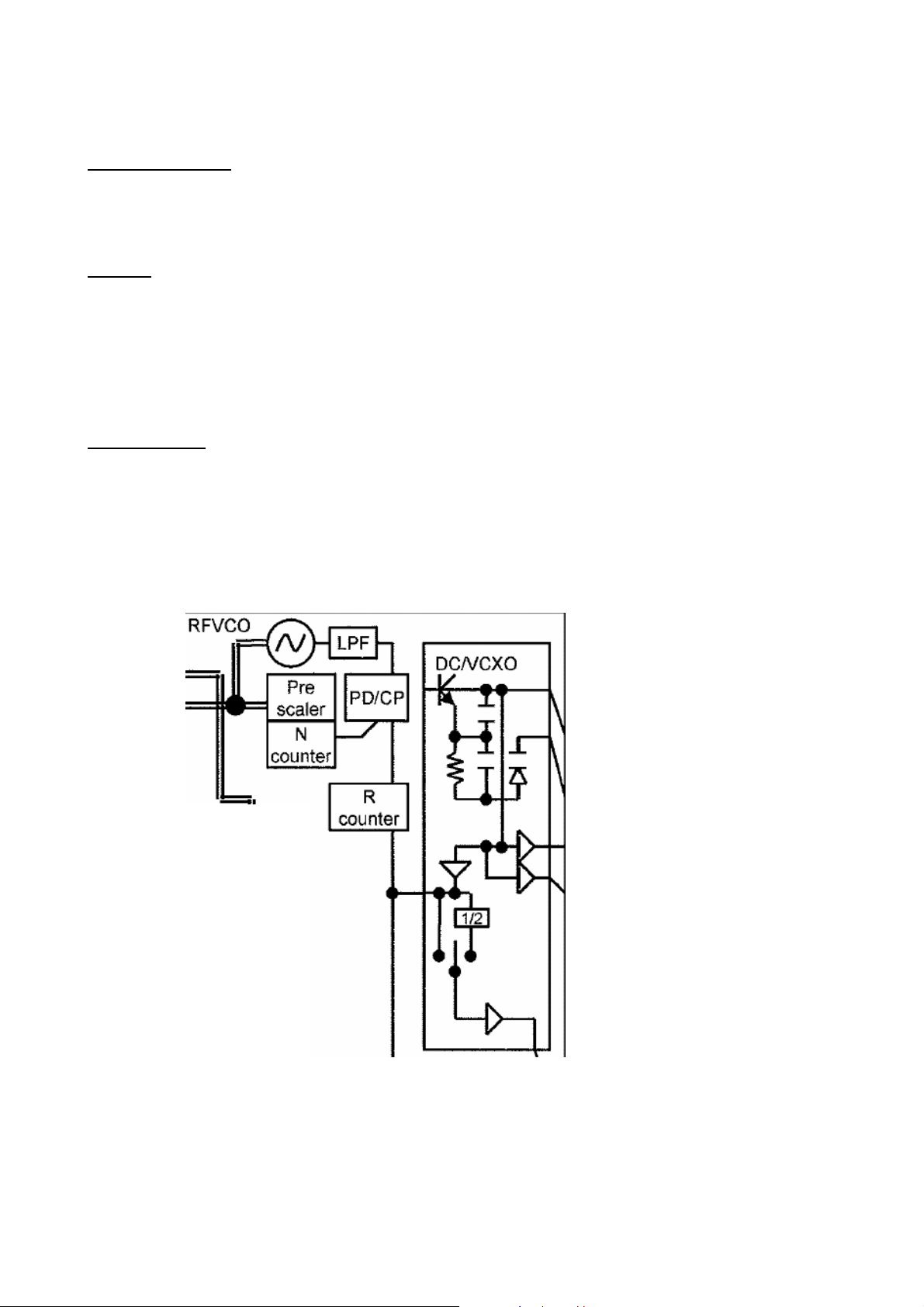
6.3 Frequency generation
Synthesizer: The discrete VCXO (26MHz)
The A70/A75 mobile is using a reference frequency of 26MHz. The generation of the 26MHz
signal is done via a VCO (Z950).
TP (test point) of the 26MHz signal is the TP 820
The oscillator output signal 26MHz_RF is directly connected to the BRIGHT IC
be used as reference frequency inside the Bright (PLL). The signal leaves the Bright IC as
RF_SIN26M
(ball G9) to be further used from the EGOLDlite (D171 (C8)).
Page 11 of 53
TD_Repair_L2.5_A70_A75_R1.0.pdf Release 1.0
(ball B9,. C9) to
Page 12
Company Confidential s Com
Copyright 2005© Siemens AG
Bright 6E
To compensate frequency drifts (e.g. caused by temperature) the oscillator frequency is
controlled by the (RF_AFC) signal, generated through the internal EGOLDlite (D171
PLL. Reference for the “EGOLD-PLL” is the base station frequency received via the
Frequency Correction Burst.
The required voltage VDD_RF2 is provided by the ASCI D361
Waveform of the AFC_PNM signal from EGOLDlite to Oscillator
VCXO Out
EGOLD In
(A10))
Signalform
EGOLD+
1 2 3
1
RF_AFC
R1
AFC_PNM
C1
2
R2
C2
R3
3
C3
GND
GND
GND
Page 12 of 53
TD_Repair_L2.5_A70_A75_R1.0.pdf Release 1.0
Page 13
Company Confidential s Com
Copyright 2005© Siemens AG
Synthesizer: LO1
First local oscillator (LO1) consists of a PLL and VCO inside Bright (D903) and an internal
loop filter
RF PLL
The frequency-step is 400 kHz in GSM1800 mode and 800kHz in EGSM900 mode due to the
internal divider by two for GSM1800 and divider by four for EGSM900. To achieve the
required settling-time in GPRS operation, the PLL can operate in fastlock-mode a certain
period after programming to ensure a fast settling. After this the loopfilter and currents are
switched into normal-mode to get the necessary phasenoise-performance. The PLL is
controlled via the tree-wire-bus of Bright VI E.
RFVCO (LO1)
The first local oscillator is needed to generate frequencies which enable the transceiver IC to
demodulate the receiver signal and to perform the channel selection in the TX part. The VCO
module is switched on with the signal PLLON. The full oscillation range is divided into 256
sub-bands To do so, a control voltage for the LO1 is used, gained by a comparator. This
control voltage is a result of the comparison of the divided LO1 and the 26MHz reference
Signal. The division ratio of the dividers is programmed by the EGOLDlite, according to the
network channel requirements.
Page 13 of 53
TD_Repair_L2.5_A70_A75_R1.0.pdf Release 1.0
Page 14
Company Confidential s Com
Copyright 2005© Siemens AG
Matrix to calculate the TX and RX frequencies A70/A75:
Band RX / TX Channels RF frequencies LO1 frequency IF freq.
EGSM 900 Receive: 0..124 935,0 - 959,8 MHz LO1 = 4*RF
EGSM 900 Transmit: 0..124 890,0 - 914,8 MHz LO1 = 4*(RF+IF) 80,0 MHz
EGSM 900 Receive: 975..1023 925,2 - 934,8 MHz LO1 = 4*RF
EGSM 900 Transmit: 975..1023 880,2 - 889,8 MHz LO1 = 4*(RF+IF) 82,0 MHz
GSM 1800 Receive: 512..661 1805,2 - 1835,0 MHz LO1 = 2*RF
GSM 1800 Transmit: 512..661 1710,2 - 1740,0 MHz LO1 = 2*(RF+IF) 80,0 MHz
GSM 1800 Receive: 661..885 1835,0 - 1879,8 MHz LO1 = 2*RF
GSM 1800 Transmit: 661..885 1740,0 - 1784,8 MHz LO1 = 2*(RF+IF) 82,0 MHz
GSM 1900 Receive: 512..810 1930,2 - 1989,8 MHz LO1 = 2*RF
GSM 1900 Transmit: 512..810 1850,2 - 1909,8 MHz LO1 = 2*(RF+IF) 80,0 MHz
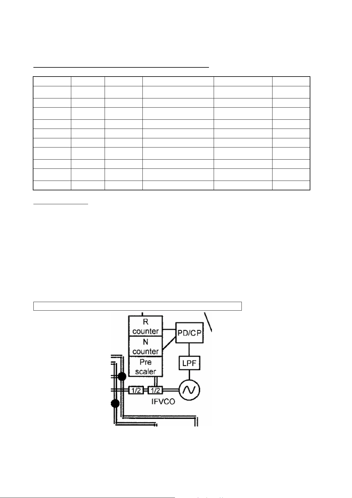
Synthesizer: LO2
The second local oscillator (LO2) consists of a PLL and VCO inside Bright (D903) and an
internal loop filter. Due to the direct conversion receiver architecture, the LO2 is only used for
transmit-operation. The LO2 covers a frequency range of at least 16 MHz (640MHz –
656MHz).
Before the LO2-signal gets to the modulator it is divided by 8. So the resulting TX-IF
frequencies are 80/82 MHz (dependent on the channel and band). The LO2 PLL and powerup of the VCO is controlled via the tree-wire-bus of Bright (EGOLDLite signals RF_DAT;
RF_CLK; RF_STR). To ensure the frequency stability, the 640MHz VCO signal is compared
by the phase detector of the 2
nd
PLL with the 26Mhz reference signal. The resulting control
signal passes the external loop filter and is used to control the 640/656MHz VCO.
The required voltage VDD_BRIGHT is provided by the ASIC D361
Page 14 of 53
TD_Repair_L2.5_A70_A75_R1.0.pdf Release 1.0
Page 15
Company Confidential s Com
Copyright 2005© Siemens AG
6.4 Receiver
Receiver: Filter to Demodulator
The band filters are located inside the frontend module (D902). The filters are centred to the
band frequencies. The symmetrical filter output is matched to the LNA input of the Bright .The
Bright 6E incorporates three RF LNAs for GSM850/EGSM900, GSM1800 and GSM1900
operation. The LNA/mixer can be switched in High- and Low-mode to perform an
amplification of ~ 20dB. For the “High Gain“ state the mixers are optimised to conversion gain
and noise figure, in the “Low Gain“ state the mixers are optimised to large-signal behavior for
operation at a high input level. The Bright performs a direct conversion mixers which are IQdemodulators. For the demodulation of the received GSM signals the LO1 is required. The
channel depending LO1 frequencies for 1800MHz/1900MHz bands are divided by 2 and by 4
for 850MHG/900MHz band. Furthermore the IC includes a programmable gain baseband
amplifier PGA (90 dB range, 2dB steps) with automatic DC-offset calibration. LNA and PGA
are controlled via EGOLDlite signals RF_DAT; RF_CLK; RF_STR
channel-filtering is realized inside the chip with a three stage baseband filter for both IQ
chains. Only two capacitors which are part of the first passive RC-filters are external. The
second and third filters are active filters and are fully integrated. The IQ receive signals are
fed into the A/D converters in the EGAIM part of EGOLDlite. The post-switched logic
measures the level of the demodulated baseband signal and regulates the level to a defined
value by varying the PGA amplification and switching the appropriate LNA gains.
From the antenna switch, up to the demodulator the received signal passes the following
blocks to get the demodulated baseband signals for the EGOLDlite:
Filter
LNA
Demodulator
PGC
D903 Bright(D903)
The required voltage VDD_BRIGHT is provided by the ASIC D361
(RF Contr N6, R6, N4). The
Page 15 of 53
TD_Repair_L2.5_A70_A75_R1.0.pdf Release 1.0
Page 16
Company Confidential s Com
Copyright 2005© Siemens AG
6.5 Transmitter
Transmitter: Modulator and Up-conversion Loop
The generation of the GMSK-modulated signal in Bright (D903) is based on the principle of
up conversion modulation phase locked loop. The incoming IQ-signals from the baseband
are mixed with the divided LO2-signal. The modulator is followed by a lowpass filter (corner
frequency ~80 MHz) which is necessary to attenuate RF harmonics generated by the
modulator. A similar filter is used in the feedback-path of the down conversion mixer.
With help of an offset PLL the IF-signal becomes the modulated signal at the final transmit
frequency. Therefore the GMSK modulated rf-signal at the output of the TX-VCOs is mixed
with the divided LO1-signal to a IF-signal and sent to the phase detector. The I/Q modulated
signal with a center frequency of the intermediate frequency is send to the phase detector as
well.
The output signal of the phase detector controls the TxVCO and is processed by a loop filter
whose components are external to the Bright. The TxVCO which is realized inside the Bright
chip generates the GSMK modulated frequency.
Modulator
Bright(D903)
The required voltage VDD_BRIGHT is provided by the ASIC D361
Filter
PD
TxVCO
Page 16 of 53
TD_Repair_L2.5_A70_A75_R1.0.pdf Release 1.0
Page 17

Company Confidential s Com
Copyright 2005© Siemens AG
6.6 Bright IC Overview
BRIGHT 6E
IC Overview
Page 17 of 53
TD_Repair_L2.5_A70_A75_R1.0.pdf Release 1.0
Page 18

Company Confidential s Com
Copyright 2005© Siemens AG
IC top view (ball overview)
Page 18 of 53
TD_Repair_L2.5_A70_A75_R1.0.pdf Release 1.0
Page 19

Company Confidential s Com
Copyright 2005© Siemens AG
6.7 Antenna switch (electrical/mechanical)
Internal/External <> Receiver/Transmitter
The A70 mobile have two antenna switches.
a) The mechanical antenna switch for the differentiation between the internal and
external antenna which is used only for RF adjustments on the board
b) The electrical antenna switch, for the differentiation between the receiving and
transmitting signals.
To activate the correct tx pathes of this diplexer, the EGOLDlite signals RF_FE_DTR_GSM
and RF_FE_DTR_DCS are required.
.
Internal/External antenna switch
to / from diplexer
The electrical antenna switch
From/to Antenna
from PA
from EGOLD
Top View :
Internal
to EGOLD
to Bright
Page 19 of 53
TD_Repair_L2.5_A70_A75_R1.0.pdf Release 1.0
Page 20

Company Confidential s Com
Copyright 2005© Siemens AG
Switching Matrix:
select mode Vsw 1 Vsw 2
GSM900/DCS1800/PCS1900 RX Low Low
EGSM TX high Low
DCS1800/PCS1900 TX Low High
Pin assignment:
1 Antenna 15 PCS1900 RX1
2 GND 16 PCS1900 RX2
3 Vsw2 (DCS1800/PCS1900 TX control) 17 GND
4 GND 18 GND
5 DCS1800/PCS1900 TX 19 GND
6 GND 20 GND
7 GND 21 GND
8 EGSM900 TX 22 GND
9 Vsw1 (EGSM900 TX control) 23 GND
10 GND 24 GND
11 EGSM900 RX1 25 GND
12 EGSM900 RX2 26 GND
13 DCS1800 RX1 27 GND
14 DCS1800 RX2 28 GND
Page 20 of 53
TD_Repair_L2.5_A70_A75_R1.0.pdf Release 1.0
Page 21

Company Confidential s Com
r
Copyright 2005© Siemens AG
Transmitter: Power Amplifier
The output signals (PCN_PA_IN , and GSM_PA_IN) from the TxVCO are led to the power
amplifier. The power amplifier is a PA-module N901 from Hitachi. It contains two separate 3stage amplifier chains GSM850/EGSM900 and GSM1800 / GSM1900 operation. It is
possible to control the output-power of both bands via one VAPC-port. The appropriate
amplifier chain is activated by a logic signal
the EGOLDLite.
To ensure that the output power and burst-timing fulfills the GSM-specification, an internal
power control circuitry is use. The power detect circuit consists of a sensing transistor which
operates at the same current as the third RF-transistor. The current is a measure of the
output power of the PA. This signal is square-root converted and converted into a voltage by
means of a simple resistor. It is then compared with the RF_RAMP1
The N901 is activated through the signal RF_TXONPA
The required voltage BATT+ is provided by the battery.
Circuit diagram
from TxVCO
RF_BAND_SW (TDMA Timer P10) which is provided by
(F12) signal.
(TDMA Timer P3).
to antenna
connecto
Page 21 of 53
TD_Repair_L2.5_A70_A75_R1.0.pdf Release 1.0
Page 22
Company Confidential s Com
Copyright 2005© Siemens AG
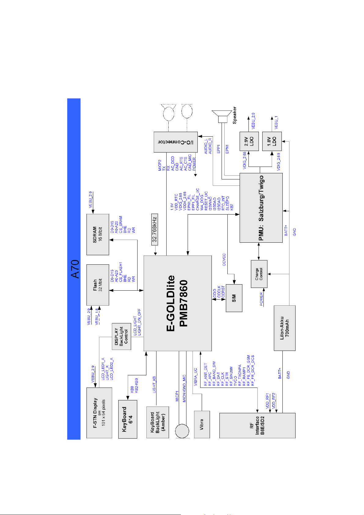
7 Logic / Control
7.1 Overview of Hardware Structure A70
Page 22 of 53
TD_Repair_L2.5_A70_A75_R1.0.pdf Release 1.0
Page 23

Company Confidential s Com
Copyright 2005© Siemens AG
7.2 Overview of Hardware Structure A75
Page 23 of 53
TD_Repair_L2.5_A70_A75_R1.0.pdf Release 1.0
Page 24

Company Confidential s Com
Copyright 2005© Siemens AG
7.3 EGOLDlite
Blockdiagram EGOLDlite
Page 24 of 53
TD_Repair_L2.5_A70_A75_R1.0.pdf Release 1.0
Page 25

Company Confidential s Com
Copyright 2005© Siemens AG
E-GOLDlite is designed as a single chip solution that integrates the digital and mixed signal
portions of the baseband. It uses a leading 0.13 µm technology with a core voltage of 1.5 V.
This allows and high performance mobile station with a large set of features at very low cost.
E-GOLDlite has a flexible set of interfaces that allows a wide choice of communication
interfaces and supports a high multimedia data rate.
E-GOLDlite is powered by C166
The E-GOLDlite is placed in a S-LF2BGA201 (a “flipchip” with 201 pins) with 0,5mm Ball-
Pitch.
The E-GOLDlite is suited for mobile stations operating in the GSM850/900/1800/1900 bands.
In the receiver path the antenna input signal is converted to the base band, filtered, and
amplified to target level by the RF transceiver chipset. The resulting differential I and Q
baseband signals are fed into the E-GOLDlite. The A-to-D converter generates two 6.5 Mbit/s
data streams. The decimation and narrowband channel filtering is done by a digital baseband
filter in each path. The DSP performs:
1. The GMSK equalization of the received baseband signal.
2. Channel decoding, which is supported by an hardware accelerator.
The recovered digital speech data is fed into the speech decoder. The E-GOLDlite supports
fullrate, halfrate, enhanced fullrate and adaptive multirate speech CODEC algorithms.
The generated voice signal passes through a digital voiceband filter. The resulting 4 Mbit/s
data stream is D-to-A converted by a multi-bit-oversampling converter, postfiltered, and
amplified by a programmable gain stage.
The output buffer can drive a handset ear-piece or an external audio amplifier.
In the transmit direction the microphone signal is fed into a programmable gain amplifier. The
prefiltered and A-to-D converted voice signal forms a 2 Mbit/s data stream. The oversampled
voice signal passes a digital decimation filter.
Speech and channel encoding (including voice activity detection (VAD) and discontinuous
transmission (DTX)) as well as digital GMSK modulation is carried out by the E-GOLDlite.
The digital I and Q baseband components of the GMSK modulated signals (48-times
oversampled with 13 MSamples/s) are D-to-A converted. The analog differential baseband
signals are fed into the RF transceiver chipset.
®
S CPU and TEAKLite® DSP cores.
Page 25 of 53
TD_Repair_L2.5_A70_A75_R1.0.pdf Release 1.0
Page 26

Company Confidential s Com
Copyright 2005© Siemens AG
The RF transceiver modulates the baseband signal to the desired frequency in the 850 MHz,
900 MHz, 1.8 GHz, and 1.9 GHz band using an I/Q modulator. The E-GOLDlite is able to
support quad band applications.
Finally, an RF power module amplifies the RF transmit signal to the required power level.
Using software, the E-GOLDlite controls the gain of the power amplifier by predefined
ramping curves (16 words, 11 bits). The E-GOLDlite communicates with the RF chip set via a
serial data interface.
The E-GOLDlite also includes battery charger support (various sensor connections for
temperature, battery technology, voltage, etc.) and a ringer buffer.
For base band operation, the E-GOLDlite supports:
• High Speed Circuit Switched Data (HSCSD) class 4
• Packet-oriented data (GPRS) class 4 with a coding scheme from 1 to 4. It provides fixed,
dynamic, and extended dynamic modes.
If the E-GOLDlite is only used as a modem, then it supports:
• High Speed Circuit Switched Data (HSCSD) class 10
Note: With a HSCSD class 10, there are a maximum of 4 received time slots and 2
transmitted time slots.
The total maximum number of received and transmitted time slots is 5.
• Packet-oriented data (GPRS) class 10 with a coding scheme from 1 to 4. It provides
fixed, dynamic, and extended dynamic modes.
Note: With a GPRS class 10, there are a maximum of 4 received time slots and 2
transmitted time slots.
The total maximum number of received and transmitted time slots is 5.
The E-GOLDlite can support Class B operation. The mobile phone can be attached to both
GPRS and GSM services, using one service at a time. During a GPRS connection Class B
enables either:
• Making or receiving a voice call
• Sending or receiving an SMS.
During voice calls or SMS, GPRS services are suspended and then resumed automatically
after the call or SMS session has ended.
E-GOLDlite is made with the Infineon C11N process using the High Voltage Threshold (HVT)
and 5 Metal Layer (5LM).
The C11N process is a 0.13 µm technology. It is used for the logic, SRAM, mixed signal, and
mixed voltage Input/Output applications.
Page 26 of 53
TD_Repair_L2.5_A70_A75_R1.0.pdf Release 1.0
Page 27

Company Confidential s Com
Copyright 2005© Siemens AG
C166S MCU
The C166S is a 16-bit CMOS (Complementary Metal Oxide Silicon) microcontroller. It
contains a CPU (Central Processing Unit) core (the MCU) and a set of peripherals.
The architecture of the MCU combines both RISC (Reduced Instruction Set Computing) and
CISC (Complex Instruction Set Computing) architecture.
• High Performance 16-Bit MCU with a four-stage pipeline:
– 38 ns minimum instruction cycle time with most instructions executed in 1 cycle (2
clock ticks)
– 192 ns multiplication (16-bit x 16-bit), 384 ns division (32-bit/16-bit)
– Parallel use of multiple high bandwidth internal data buses
– Register based design with multiple variable register banks
– Single cycle context switching support
– 16 MBytes linear address space for code and data (von Neumann architecture)
– System stack cache support with automatic stack overflow/underflow detection.
• Control Oriented Instruction Set with High Efficiency:
– Bit, byte, and word data types
– Flexible and efficient addressing modes for high code density
– Enhanced boolean bit manipulation with direct addressing of 6 Kbits for peripheral
control and user defined flags
– Hardware traps to identify exception conditions during runtime
– HLL support for semaphore operations and efficient data access.
• External Bus Interface:
– Demultiplexed bus configurations
– Segmentation capability and chip select signal generation
– 8-bit or 16-bit data bus
– Bus cycle characteristics selectable for five programmable address areas.
• 16-Priority-Level Interrupt System:
– Up to 112 interrupt nodes with separate interrupt vectors
– 16 priority levels and 8 group levels.
• 16-Channel Peripheral Event Controller (PEC):
– Interrupt driven single cycle data transfer
– Transfer count option (standard MCU interrupt after programmable number of PEC
transfers)
– Long Transfer Counter
– Channel Linking
– Eliminates overhead for saving and restoring system state for interrupt requests.
Page 27 of 53
TD_Repair_L2.5_A70_A75_R1.0.pdf Release 1.0
Page 28

Company Confidential s Com
Copyright 2005© Siemens AG
• DPRAM:
– Internal 16-bit dual port RAM with a 1K x 16-bit size.
• SCU (System Control Unit):
– Handles the boot and sleep mode of the core
– Provides a watchdog timer.
The architecture of the C166S combines the advantages of both RISC (Reduced Instruction
Set Computing) and CISC (Complex Instruction Set Computing) processors in a wellbalanced way. C166S based derivatives not only integrate a powerful MCU (Central
Processing Unit) core and a set of peripheral units into one chip, but also connects the units
in a very efficient way. One of the four buses used concurrently on the C166S is the Internal
Bus Interface, an internal representation of the external bus interface. This bus provides a
standardized method of integrating application-specific
peripherals to produce derivatives of the standard C166S.
The Principle Elements of a C166S Based System
• MCU block including the configurable Interrupt/PEC controller and debug and break logic
• Configurable dual port RAM
• Configurable Interrupt/PEC controller
• All interfaces for system (on chip) integration, including X-Bus, PD peripheral bus, Local
Memory bus (for ROM or SRAM).
The C166 architecture allows instruction execution and data access from all memory
locations. This includes X-Bus, local memory bus, dual port and external memories.
All four bus Interfaces of the MCU (X-Bus, LM Bus, RAM Bus and PD Bus) are operated
on at the same time by the MCU.
TEAKLite:
The TEAKLite core has 16-bit data and 16-bit program memory accesses, a high
performance fixed-point DSP core, and low power consumption.
The core consists of a high performance processing unit including a full featured bitmanipulation unit, RAM and ROM addressing units, and program control logic. The core has
an improved set of DSP and general microprocessor functions to meet application
requirements. The programming model and instruction set are optimized for generation of
efficient and compact code.
The Computation Unit consists of a 16 by 16 multiplier unit with a 32-bit product and a 36-bit
ALU with two accumulator registers A0 and A1.
Page 28 of 53
TD_Repair_L2.5_A70_A75_R1.0.pdf Release 1.0
Page 29

Company Confidential s Com
Copyright 2005© Siemens AG
The Bit Manipulation Unit consists of a full 36-bit barrel shifter, an exponent unit, a bit-field
operation unit, two 36-bit accumulator registers B0 and B1, and a shift value register.
The Data Address Arithmetic Unit performs all the address storage and address calculation
necessary for accessing the data and program memories. It also supports a software stack
pointer, loop counter, and min/max operations.
The key features of TEAKlite core are as follows:
• 16-bit fixed-point DSP core
• 16 x 16-bit 2’s complement parallel multiplier with a 32-bit product
• Single cycle multiply-accumulate instructions
• 36-bit ALU
• 36-bit left/right barrel shifter
• Four 36-bit accumulators
• Software stack residing in the data RAM
• User-defined registers off-core
• Three high-active interrupt input lines INT0, INT1, and INT2
• Automatic context switching by interrupts
• Up to 16-bit Bit Field Operations (BFO)
• Three modes for power saving features: Operational, Idle, and Sleep.
• The maximum Frequency is 104 MHz. The TEAKlite core clock is scalable to lower
frequencies.
In the DSP Firmware are implemented the following functions:
The High Speed Circuit Switched Data (HSCSD) class 4 is supported.
The packet-oriented data (GPRS) class 4 is supported with a coding schemes from 1 to 4. It
provides fixed, dynamic and extended dynamic modes.
If the E-GOLDlite is used as a modem, the HSCSD and GPRS class 10 is supported. The
packet-oriented data (GPRS) class 10 is supported with a coding schemes from 1 to 4. It
provides fixed, dynamic, and extended dynamic modes.
Synchronisation and Measurements
• Scanning of channels (measurement of the field strengths of neighboring base
stations)
• Detection and evaluation of Frequency Correction Bursts.
Equalization
There is equalization of GMSK Normal Bursts and Synchronization Bursts with bit-by-bit
soft output.
Channel Coder/Decoder
There are Channel Coders/Decoders for 2.4kbits/s, 4.8kbits/s, 9.6kbits/s, and 14.4kbits/s.
Page 29 of 53
TD_Repair_L2.5_A70_A75_R1.0.pdf Release 1.0
Page 30

Company Confidential s Com
Copyright 2005© Siemens AG
Speech
Voiceband
Also the functionality and the internal and external interfaces of the Audio Scheduler is
implemented in DSP firmware of E-GOLDlite.
Real Time Clock (integrated in the E-GOLDlite):
The real time clock (degree of accuracy 150ppm) is powered via a seperate voltage regulator
inside the PMU. Via a capacitor, data is kept in the internal RAM during a battery change for
at least 30 seconds. An alarm function is also integrated with which it is possible to switch the
phone on and off.
• A Speech Coder-Decoder: FR, EFR, AMR Narrow Band, or HR.
• Discontinuous transmission (DTX)
• Voice activity detection (VAD)
• Comfort noise generation (CNG).
• Generation of tones and side-tones
• Ringer tone generation
• Echo Cancellation (handsfree) with noise reduction
7.4 SRAM
Memory for volatile data
Memory Size: A70/A75 - 16 Mbit
Data Bus: 16Bit
7.5 FLASH
Memory Size: A70 - 32 Mbit (4Mbyte) A75 - 64 Mbit (8Mbyte)
Data Bus: 16 Bit
7.6 SIM
SIM cards with supply voltages of 1.8V and 3V are supported.
7.7 Vibration Motor
The vibration motor is mounted in the lower case. The electrical connection to the PCB is
realised with pressure contacts.
Page 30 of 53
TD_Repair_L2.5_A70_A75_R1.0.pdf Release 1.0
Page 31

Company Confidential s Com
Copyright 2005© Siemens AG
7.8 Display Modules
The A70 display has a resolution of 101x64 pixels b/w. It contains a passive addressed FSTN panel. The A75 display has a resolution of 101x80 pixels with a colour depth of 256 or
4096 colours. The colour depth is switch-selectable by software. It contains a passive
addressed STN panel where the colours are generated by colour filter (C-STN, Colour-Super
Twisted Nematic). Different sources are used for the displays. The modules use different
LCD-controllers. In order to guarantee a very efficient illumination the Amber LEDs are
mounted on a PCB on the module. In addition, all passive components necessary to drive an
LCD are assembled on the module PCB. Further, the hardware coding is also implemented
on the module PCB. Thus, the only interconnections to the Siemens PCB are the data lines
and the power supply lines of the controller and the amber LEDs. The interface is realised by
a spring connector with 10 interconnections, which is assembled on the Siemens PCB.
Pin Name Remarks
1 LCD_CS Chip select
2 LCD_RESET Reset
3 LCD_RS Register select
4 LCD_CLK Clock
5 LCD_DAT Data line
6 2.9V Power supply display controller
7 GND GND
8 LCD_LED2_A Power supply display led 2
9 LIGHT_K Switched GND for display led 1 and led 2
10 LCD_LED1_A Power supply display led 1
Required voltage for the display illumination is LCD_LED1_A and LCD_LED2_A.
Page 31 of 53
TD_Repair_L2.5_A70_A75_R1.0.pdf Release 1.0
Page 32

Company Confidential s Com
Copyright 2005© Siemens AG
The voltage regulator N280 with a nominal output voltage of 2.8V is used. With the signal
LIGHT_LCD
Required voltage for the display controller VEBU_2.9V.
The voltage regulator N308 with a nominal output voltage of 2.9V is used
(P1) the illumination for the display is controlled.
Page 32 of 53
TD_Repair_L2.5_A70_A75_R1.0.pdf Release 1.0
Page 33

Company Confidential s Com
Copyright 2005© Siemens AG
7.9 Illumination – Keyboard
The LED´s are mounted on the upper side of the PCB. The illumination of the keypad will be
done via high-brightness LEDs (colour: amber, type: top-shooter, driven by 6 mA / LED). The
light is switched via switches inside the EGOLDlite. With the signal LIGHT_KB
illumination for the keyboard is controlled.
(R5) the
Page 33 of 53
TD_Repair_L2.5_A70_A75_R1.0.pdf Release 1.0
Page 34

Company Confidential s Com
Copyright 2005© Siemens AG
8 Acoustic
The speaker module is designed to provide good performance for mobile handsfree and
sound ringer. The speaker module is a system which has a closed front volume with soundoutlets towards the ear of the user. The speaker is partly hidden behind the display to save
length of the phone. The back volume of speaker module is using the unused air between the
antenna and the PCB. The speaker module is connected to the SAR-frame and contacted via
two bending springs to the PCB. For avoiding any interference between antenna and
earpiece, there is an antenna reference plate soldered behind the speaker at the PCB. In
ringer mode acoustic shock is avoided by using ramping of the ringer level.
The microphone is built in the Mounting Frame Lower Part and is mechanically fixed with a
rubber seal (gasket). The contact on the PCB is realised via spiral springs, which are
integrated in the gasket. Because of usage of Unidirectional Microphone, the gasket has a
front- and a back sound-inlet hole. The front sound-inlet is acoustically tighten connected with
a sound-inlet at the rear-side of the mounting frame lower part. The back sound-inlet is
acoustically tighten connected with a sound-inlet at the bottom-side of the mounting frame
lower part. The gasket of the microphone has a asymmetrical shape in order to provide nonrotating, guaranteed covering of the sound-inlets of mounting frame lower part to the
corresponding sound-inlets at microphone gasket.
The buzzer and the keypad clicks will be realized over the earpiece.
The standard sounds will be generated by the EGOLDlite, the advanced sounds will be
generated via firmware running on the DSP.
9 Power Supply, Battery and Charging
All the important functions for the power supply of the phone are carried out by the power
supply ASIC.
The POWER-pin of the I/O-Connector is for charging the battery with an external power
supply.
Page 34 of 53
TD_Repair_L2.5_A70_A75_R1.0.pdf Release 1.0
Page 35

Company Confidential s Com
Copyright 2005© Siemens AG
9.1 Power Supply ASIC
The power supply ASIC will contain the following functions:
Powerdown-Mode
Sleep Mode
Trickle Charge Mode
Power on Reset
Digital state machine to control switch on and supervise the uC with a watchdog
Voltage regulator
Low power voltage regulator
Additional output ports
Voltage supervision
Temperature supervision with external and internal sensor
Battery charge control
TWI Interface (I2C interface)
Bandgap reference
Audio multiplexer
Audio amplifier stereo/mono
16 bit Sigma/Delta DAC with Clock recovery and I2S Interface
Power Supply Operating modes:
The ASIC can be used in different operating modes:
Mode Pin Requirements Description
Power down
mode with
minimum activity
Start Up Mode ON_OFF
Full operating
mode
ON/OFF
ON/OFF2
VDD_CHARGE
ON_OFF2
VDD_CHARGE
CHARGE_UC
In power down mode the current consumption of the ASIC is
very low. The inputs for switch on conditions (Pin ON/OFF,
ON/OFF2,VDD_CHARGE), the LPREG, Bandgap reference,
and the POR cells are active. All other blocks are switched off,
so the battery is not discharged. This state is called “phone
off.
Start Up Mode can be initiated by ON_OFF or ON_OFF2. In
this mode a sequential start-up of references (this includes the
reference buffer and the biasing cell), oscillator., voltage
supervision and regulators is controlled by digital part. In
failure case (undervoltage, overvoltage or time out of the µC
reaction)., the ASIC is shut down.
All blocks are active. Trickle charge is switched off. The blocks
fast charge and charge monitor can be active only in this
mode. These modes will be activated with VDD_CHARGE or
CHARGE_UC. The name of this mode is “phone on” or “active
mode”. The border between the startup phase and the active
mode is the rising edge of the RESETN signal. This will allow
the uC to start working.
Page 35 of 53
TD_Repair_L2.5_A70_A75_R1.0.pdf Release 1.0
Page 36

Company Confidential s Com
Copyright 2005© Siemens AG
Mode Pin Requirements Description
Active Mode
(submode of Full
operating mode)
Sleep Mode with
special low
current
operating mode
for the LDOs
(submode of Full
operating mode)
Trickle charge
mode to be able
to support
charging of the
battery
In this mode, the uC controls the charging block and most of
the failure cases. The ASIC can be controlled by the TWI
interface, interrupts can be sent by the ASIC. Further, the
temperature and the voltages are supervised (in case of
failure, the uC will be informed). In case of watchdog failure,
overvoltage or power on reset, the ASIC will be switched off
immediately. The mono and stereo audio block can be
switched on in active mode.
SLEEP1_N
TC_ON
CHARGE_uC
VDD_CHARGE
EXT_PWR
A low level at the pin SLEEP1_N will switch the phone from
the mode “PHONE ON” to sleep mode. This mode can be
activated out of the active mode. In sleep mode trickle charge
(TC_ON), fast charge (CHARGE_UC), supply overvoltage
detection, supply undervoltage detection, audio function are
switched off. LDO undervoltage detection, clock and all
reference voltages are active. LDOs are working in low current
mode. The possibility to supply the ASIC from VDD_CHARGE
with the internal LDO is switched off. Only the battery can be
used for supply. This mode is called “phone stand-by”.
In case of a rising edge at VDD_CHARGE the ASIC goes
from power down to interim mode. In this mode, the oscillator
and the reference are started. The fuses are read in. If the
voltage is high enough (after a delay time of 1 ms to filter a
ringing), the signal EXT_PWR is going to H and the power up
continues. The ASIC shuts off if the voltage is below
threshold. In Trickle Charge Mode, first the charge unit starts
and charges the battery in case of undervoltage. After
reaching this threshold voltage or if the battery has enough
voltage from the beginning, a start up similar to the regular
startup mode is initiated. In case of voltage drop under battery
threshold, the first trickle charging can be started again until
the Active Mode is entered. In this case, the internal VDDREF
regulator, the reference generator and oscillator are started
and the ASIC is supplied by VDDREF. If any failure is
detected, the ASIC is switched off.
Page 36 of 53
TD_Repair_L2.5_A70_A75_R1.0.pdf Release 1.0
Page 37

Company Confidential s Com
Copyright 2005© Siemens AG
Power Supply Functions:
Functions Pin Requirements Implementation/Sequence
Switching on the
mobile phone
Watchdog
monitoring
Power-On-Reset
(POR)
Voltage Supply
Logics
ON_OFF,
ON_OFF2,
VDD_CHARGE
WDOG As soon as the first WDOG pin rising is detected during the
RESET_N
RESET2_N
REG1
(2.65V)
There are 3 different possibilities to switch on the phone by
external pins:
- VDD_CHARGE with rising edge after POR or high level at
end of POR signal
- ON/OFF with falling edge
- ON/OFF2 with rising edge
In order to guarantee a defined start-up behaviour of the
external components, a sequential power up is used and the
correct start up of these blocks is supervised. In active mode,
a continuous signal at watchdog is needed to keep the
system running. If the signals fails, the ASIC will switch to
power down mode. It must be guaranteed that each start-up
condition does not interfere and block the other possible
startup signals. In case of failure during start-up, the device
will go back to power down mode. To guarantee that
VDDCHARGE is always sensed we must be able to detect
whether the VDDCHARGE will have a rising edge during
POR (this can happen in case of an empty battery). Therefore
this signal is sensed as level sensitive at the end of POR and
edge sensitive after POR signal.
TE4 timer, the device start the watchdog monitoring
procedure. Standard switch off of the phone is the watchdog.
The first edge of watchdog is rising. If a falling edge is
detected as the first transient the device will go to power
down mode again and the whole phone is switched off. Rising
and falling edges must be detected alternated. With any edge
on WDOG pin a counter will be loaded. The next - compared
to the previous edge - inverted edge must occur between end
of T1, and end of T2. If the signal occurs before end of T1 or
is not detected until end of T2, the device will go to power
down mode immediately after the violation of the watchdog
criteria occurs.
T1 min. 0,327s/ typ. 0,360s/ max. 0,400s
T2 min. 2,600s/ typ. 2,860s/ max. 3,178s
To guarantee a correct start-up of the ASIC, a power on reset
is needed at first power supply ramping. Therefore a
static/dynamic power on reset circuit is added, which creates
a reset each time the power supply is connected. After POR
the ASIC starts up the reference and the oscillator, read in the
fuse content and goes back to power down mode. If the
power supply will drop under the POR threshold V
synchronous reset is done and the ASIC will go to power
down mode independently of the previous operating mode.
V
th,POR_L
The linear controller is designed for 2.65V(±2%) and a
maximum load current of 140 mA.
Voltage and current for the external Logic is supplied from the
internal 2.65V logic regulator. The operating voltage VREG1
is kept constant up to the maximum rated load current. A
reference voltage for the regulator circuit is generated from a
bandgap reference
= min. 2.38/ typ. 2.43/ max. 2.48V
th,POR_L
a
Page 37 of 53
TD_Repair_L2.5_A70_A75_R1.0.pdf Release 1.0
Page 38

Company Confidential s Com
Copyright 2005© Siemens AG
Functions Pin Requirements Implementation/Sequence
Voltage Supply
Logics
Voltage Supply
Logics
Voltage Supply
RF
Voltage Supply
RF
Voltage Supply
Audio
REG2
(1,5V)
REG3
(2.65V)
VREGRF1,
SLEEP1_N,
SLEEP2_N,
POWER_ON
VREGRF2,
RF_EN,
RESET_N
VREGA The linear controller is designed for 2.9V(min. 2.84V, max.
The linear controller is designed for 1.5V (±2%) and a
maximum load current of 300 mA.
The output voltage can be adjusted to four different values
with TWI register by the µC. The selectable values are
1.5(default), 1.82, 1.92 and 2.0V.
The REG2 supplies the Baseband Processor.
The linear controller is designed for 2.65V(±3%) and a
maximum load current of 140 mA.
It will consist basically of an internal operation amplifier, an
integrated p-channel output transistor as well as a capacitor
(C = 2.2µF) for stabilising the voltage. The required reference
voltage for the regulating circuit will be generated internally
via a band gap. The negative feedback of the regulating
circuit shall be done via chip-internal resistances.
The linear controller is designed for 2.755V (±2%) and a
maximum load current of 150 mA. The output voltage can be
adjusted to three different values with TWI register by the µC.
The selectable values are 2.755V(default), 2.54V, and 2.85V.
Voltage and current for RF-VCO and Transceiver is supplied
from the internal 2.755V LDO. The operating voltage RF1LDO
is kept constant up to the maximum rated load current. A
reference voltage for the regulator circuit is generated from a
bandgap reference. A low noise must be guaranteed.
RF1LDO is controlled by SLEEP1_N and SLEEP2_N. If one
of them is set to high, the regulator is enabled. The control
method can be modified by TWI interface between external
and internal control mode. If internal control mode is set,
RF1LDO can only be enabled by TWI bit. In external mode,
RF1LDO can only be enabled by SLEEP1_N or SLEEP2_N.
RF1LDO is released with rising edge of POWER_ON signal.
The linear controller is designed for 1.53V (±2%) and a
maximum load current of 180 mA. The output voltage can be
adjusted to three different values with TWI register by the µC.
The selectable values are 1.53V(default), 2.70V, and 2.85V.
Voltage and current for RF-VCO and Transceiver is supplied
from the internal 1.53V LDO. The operating voltage RF2LDO
is kept constant up to the maximum rated load current. A
reference voltage for the regulator circuit is generated from a
bandgap reference. A low noise must be guaranteed.
RF2LDO is controlled by RF_EN. If it is set to high, the
regulator is enabled. The control method can be modified by
TWI interface between external and internal control mode. If
internal control mode is set, RF2LDO can only be enabled by
TWI bit. In external mode, RF2LDO can only be enabled by
RF_EN.
RF2LDO is released with rising edge of RESET_N signal.
2.96V) and a maximum load current of 190 mA.
VDDA is used for the whole stereo analog supply. The DAC
digital (VDDDAC), Low Noise Bandgap, Mono- and
Stereoamplifier supplies are connected to VREGA or VBAT or
an external LDO at 2.9V +/-5%. The AUDIO performances are
guaranteed only, if the VREGA supplies all the stereo path.
VREGA is controlled with TWI registers directly by the µC.
Page 38 of 53
TD_Repair_L2.5_A70_A75_R1.0.pdf Release 1.0
Page 39

Company Confidential s Com
Copyright 2005© Siemens AG
Functions Pin Requirements Implementation/Sequence
Voltage Supply
RTC
Voltage Supply
SIM
Charge Support CHARGE_UC,
Voltage
supervision
Supervision of
REG1 and
REG2
Powersupply
supervision
VDDA
supervision
TD_Repair_L2.5_A70_A75_R1.0.pdf Release 1.0
VLPREG The linear controller is designed for 2.00V(min. 1.9V, max.
2.1V) and a maximum load current of 1 mA.
The output voltage can be adjusted to four different values
with TWI register by the µC. The selectable values are
2.00(default), 1.82, 1.92 and 2.07V. LP-LDO is always
working and will switch of only with POR signal.
VREGSIM The linear controller is designed for 2.9V(min. 2.84V, max.
2.96V) and a maximum load current of 60 mA. The output
voltage can be adjusted to a different value with TWI register
by the µC to 1.8V(min. 1.76V, max. 1.84V).
This regulator can be activated by TWI register, but only in
active mode. If the regulator is in power down, the output is
pulled down by a transistor to avoid electrostatic charging of
VREGSIM.
A charge support will be integrated for controlling the battery
CHARGE,
VDDCHARGE,
AVDD, SENSE_IN,
TBAT
The levels of regulator REG1, REG2, REGA, SIM_LDO, and
REG1
REG2
VDD If the battery voltage VDD exceeds VDD_high everything is
VDDA To provide a short circuit protection at output of VDDA and
charge function. It consists basically of a temperature sensor,
an external charge FET, an integrated High-side driver for the
external FET with an external resistor between the source
and the gate of the charge FET.
In the case of a rising edge at the CHARGE_UP the power
source will be switched on. In this way the charge FET
becomes conducting, provided that the integrated
temperature comparator does not give the signal for extreme
temperature and that no overvoltage is present at the VDD. In
the case of falling slope at the CHARGE_UP, the current
source is switched off and the pull-up resistor will make sure
that the charge FET is blocked after a finite time.
Temperature switchoff becomes effective at approx. T>60°C.
also the supply voltage VBAT are supervised with
comparators.
In active mode the regulators are supervised permanently. If
the voltage is under the threshold, the pin RESET_N stay Low
and the ASIC go back to the power down mode. If the voltage
is longer than Tmin under threshold voltage, the RESET_N is
going to Low (Missing Watchdog signal -> phone switched
off). The level of regulator REG1 and REG2 will be
supervised permanently. If the voltage doesn’t reach the
threshold value at switch on, the RESET_N pin will stay low
and the ASIC will go back to power down mode. The voltages
are sensed continuously and digitally filtered with a time
constant Tmin. If the regulator voltage is under threshold
longer than Tmin, the RESET_N signal change to low and the
uC will go to RESET condition (Missing Watchdog signal ->
phone switched off).
switched off immediately within 1µs. Only the pullup circuitry
for the external charge PMOS are active and will discharge
the gate of the external PMOS
output of stereo buffer a voltage supervision is implemented.
If the VDDA output is less then this threshold, the VDDA will
be switched off for 128ms. After this time the VDDA will be
started again. The VDDA supervision starts 60ms after
startup of VDDA.
Page 39 of 53
Page 40

Company Confidential s Com
Copyright 2005© Siemens AG
Functions Pin Requirements Implementation/Sequence
Battery
temperature
supervision
Device
temperature
supervision
Analog switch
Outport
TWI Interface TWI_CLK,
Audio mode
functions
Audio Mono
Mode
Charging is stopped, when overtemperatur occurs. Within
128ms, 3 values are measured. When these 3 values are
identical status can be changed. The supervision is active in
fast charge or trickle charge mode. Voltage on pin TBAT
becomes smaller when temperature increases. If Vbat <
(Vref_exe - Vhyst) charging is disabled. Only when Vtbatt >
Vref_exe charging is enabled again.
To protect the ASIC, the temperature is supervised. The
temperature is polled every 128ms and is filtered as in battery
temperature supervision. If overtemperatur is detected, a bit
in the STATUS register is set and an interrupt is generated.
Monitoring is started only in active mode.
The level can be defined by the bit out_port_high of the TWI
register. The high level can be derived of VREG2 or VREG3.
Additional a pulldown transistor is connected to this node.
The TWI interface is an I2C compatible 2-wire interface with
TWI_DATA,
TWI_INT
Four audio amplifiers are integrated to support these modes:
VREGA
MONO1
MONO2
VREFEX_M
an additional interrrupt pin to inform the µC about special
conditions.
The interface can handele clock rates up to 400 kHz. The
device adress is 010001B (31H)
1. Supply the speaker in the phone with audio signals
including the possibility of handsfree and antipop switch
on and off. This is the AUDIO MONO MODE.
2. Supply the speaker in the phone with ringing signal
(RINGER MODE)
3. Transfer a key click, generated in digital part to the
speaker. (KEY-CLICK FUNCTION)
4. Supply of stereo head set with stereo signal with short
circuit protection. This is called the AUDIO STEREO
MODE. These different modes with gain and multiplexing
can be controlled via TWI. Also the output can be
switched to TRI-STATE via TWI interface.
This mode is the main function of the amplifier. The two
amplifiers are used as differential mono amplifier to drive the
speaker in the phone as external load. This differential
approach allows delivering an optimum of power to the
speaker, also in low voltage mode. Both amplifier paths are
inverting amplifiers with external AC coupling at the input to
compensate offset failures. The gain can be adjusted with the
TWI interface. The output stage of the amplifiers must be able
to drive a low impedance load as a external speaker for the
handsfree application.
General parameters: Gain can be adjusted for each channel
separately in steps of 1.5dB in the range of 21dB to –54 dB
and in steps of 3 dB in the range of –54dB to –75dB. The
signals for the amplifier are connected via an audio
multiplexer with 3 pairs of input signals.
Page 40 of 53
TD_Repair_L2.5_A70_A75_R1.0.pdf Release 1.0
Page 41

Company Confidential s Com
Copyright 2005© Siemens AG
Functions Pin Requirements Implementation/Sequence
Audio Stereo
Mode
Ringer function RINGIN In ringer mode the ringing signal is transferred via the
Key click
function
Audio Multiplex
Matrix
VDDSTEREO
STEREO1
STEREO2
STEREOM
Pushing a key of the phone can be combined with a key click.
AUDIOA1
AUDIOA2
AUDIOB1
AUDIOB2
AUDIOC1
AUDIOC2
For stereo mode 2 single ended buffers are used. These
buffers will be supplied by the additional regulator with 2.9
Volt to be more stable against the GSM ripple on the battery
voltage. Also reference voltage for the buffers is generated by
a high precision, low noise bandgap reference for better
performance. An external capacitor is needed to filter this
reference additionally. The gain steps for the programmable
gain amplifier are identical with the mono amplifier.
Nokeyclick and ringer needed for the stero part. Gain can be
controlled with the TWI. The connected speaker has an
impedance of typical 16 Ohm. To guarantee a ANTI-POP
noise a digital startup is implemented. This will allow a soft
start of the VMID and creates a “clean” audio band during the
startup. For eliminating external coupling capacitors for the
speaker, an additional amplifier creates virtual ground (for
both speakers). Accordingly to this, the max current of the
virtual ground has to be the double of the normal output
amplifier. Due to the power amplifier offset a DC current
appear in the headset. Gain can be adjusted for each channel
separately in steps of 1.5dB in the range of 21dB to –54 dB
and in steps of 3 dB in the range of –54dB to –75dB
amplifier to the speaker to eliminate the additional buzzer.
The speaker is controlled with a rectangular signal RINGIN.
Input signal is digital signal with variable frequency. Amplitude
is adjusted by TWI register.
For start-up a smaller time constant must be used to allow a
fast switch on behaviour. Ringing function can be started at
any time. If the audio is off, the start-up is done with RINGER
time constant. If audio is starting with AUDIO start-up, the
time constant is switched to RINGER mode, too. If the audio
amplifier is already up and running, the RINGIN is connected
to the amplifier and audio sigal is muted due to open
multiplexer.
This function is also realized with the audio amplifier in pulsed
mode. The ASIC creates a digital PWM signal. Frequency of
the PWM signal is 3.5 kHz.
The start-up is similar to the ringer function. If the audio is off,
the start-up is done with KEYCLICK time constant. If audio is
starting with AUDIO start-up, the time constant is switched to
KEYCLICK mode, too. If the audio amplifier is already up and
running, the KEYCLICK is connected to the amplifier and
audio sigal is muted due to open multiplexer.
Each of the three input sources should be switched to Mono
and Stereo outputs. Furthermore a conversion can be done.
Following sources:
- Mono differential
- Mono Single Ended (both channels parallel)
- Stereo
The DAC can be switched off for using the analog external
inputs. This principle will allow to do each combination and
have different modes for stereo and mono in parallel.
Page 41 of 53
TD_Repair_L2.5_A70_A75_R1.0.pdf Release 1.0
Page 42

Company Confidential s Com
Copyright 2005© Siemens AG
Functions Pin Requirements Implementation/Sequence
I2S Interface CLO,
WAO,
DAO
Audio DAC
PLL VDDPLL
VDDDAC For digital to analog conversion a 16 bit sigma delta converter
PLLOUT
The I2S Interface is a three wire connection that handels two
timemultiplexed data channels. The three lines are the clock
(CLO), the serial data line (DAO) and the word select line
(WAO). The master I2S also generates the appropriate clock
frequncy for CLO set to 32 times the sampling rate (FS)
is used. Digital input signal is delivered with a I2S interface.
The I2S interface should be 16 bit format. To be able to work
with allpossible operating modes, the sampling frequency can
vary from 8kHz to 48kHz. The performance of the audio
output signal must be guaranteed over the full range the
human ear is able to hear. This means for FS=8kHz the noise
at frequencies higher than FS/2 must be suppressed. This is
done by DSP in a single ended 2
clock for the I2S will be varied accordingly to the sampling
frequency. Therefore a clock recovery based on CLO signal
of the I2S can be implemented. This clock recovery must
smooth any jitter of this clock to reduce the noise of the DAC.
The PLL will have three frequency modes to produce a
32xCLO clock for the DSP and the DAC. The loop filter is
realised with an external RC circuit. This PLL also contains a
lock detector circuit.
nd
order Low Pass filter. The
9.2 Battery
As a standard battery a LiIon battery with a nominal capacity of 3,7 Volt/700mAh is used.
Page 42 of 53
TD_Repair_L2.5_A70_A75_R1.0.pdf Release 1.0
Page 43

Company Confidential s Com
Copyright 2005© Siemens AG
9.3 Charging Concept
Charging current
Charging control signal
9.3.1.1 Charging Concept
General
The battery is charged in the unit itself. The hardware and software is designed for LiIon with
4.2V technology.
Charging is started as soon as the phone is connected to an external charger. If the phone is
not switched on, then charging takes place in the background (the customer can see this via
the “Charge” symbol in the display). During normal use the phone is being charged
(restrictions: see below).
Charging is enabled via a PMOS switch in the phone. This PMOS switch closes the circuit for
the external charger to the battery. The EGOLDlite takes over the control of this switch
depending on the charge level of the battery, whereby a disable function in the POWER
SUPPLY ASIC hardware can override/interrupt the charging in the case of over voltage of the
battery (only for Manganese Chemistry Battery types e.g. NEC).
With the new slim Lumberg IO connector we lose the charger recognition via SB line. Now
we measure the charge current inside the POWER SUPPLY ASIC with a current monitor.
The charging software is able to charge the battery with an input current within the range of
350-600mA. If the Charge-Fet is switched off, then no charging current will flow into the
battery (exception is trickle charging, see below).
For controlling the charging process it is necessary to measure the ambient (phone)
temperature and the battery voltage. The temperature sensor will be an NTC resistor with a
nominal resistance of 22kΩ at 25°C. The determination of the temperature is achieved via a
voltage measurement on a voltage divider in which one component is the NTC. The NTC for
the ambient temperature will be on the PCB (26 MHz part).
Page 43 of 53
TD_Repair_L2.5_A70_A75_R1.0.pdf Release 1.0
Page 44

Company Confidential s Com
Copyright 2005© Siemens AG
Measurement of Battery, Battery Type and Ambient Temperature
For the conversion of signals like battery voltage, battery type, temperature, EGOLDlite
provides identical measurement interfaces. Measurement circuit is consisting of external
sensing components and integrated analog multiplexers and switches. Through
corresponding switch settings, the measured signal is passed to input of ADC. 12-bit
conversion results are readout by µc and used for charging control.
Charging Characteristic of Lithium-Ion Cells
LiIon batteries are charged with a U/I characteristic, i.e. the charging current is regulated in
relation to the battery voltage until a minimal charging current has been achieved. The
maximum charging current is approx. 600mA, minimum about 100mA. The battery voltage
may not exceed 4.2V ±50mV average. During the charging pulse current the voltage may
reach 4.3V. The temperature range in which charging of the phone may be started ranges
from 5...40°C, and the temperature at which charging takes place is from 0...45°C. Outside
this range no charging takes place, the battery only supplies current.
Trickle Charging
The POWER SUPPLY ASIC is able to charge the battery at voltages below 3.2V without any
support from the charge SW. The current will by measured indirectly via the voltage drop
over a shunt resistor and linearly regulated inside the POWER SUPPLY ASIC. The current
level during trickle charge for voltages <2.8V is in a range of 20-50mA and in a range of 50100mA for voltages up to 3.75V. To limit the power dissipation of the dual charge FET the
trickle charging is stopped in case the output voltage of the charger exceeds 10 Volt. The
maximum trickle time is limited to 1 hour. As soon as the battery voltage reaches 3.2 V the
POWER SUPPLY ASIC will switch on the phone automatically and normal charging will be
initiated by software (note the restrictions on this item as stated below).
Normal Charging
For battery voltages above 3.2 Volt and normal ambient temperature between 5 and 40°C the
battery can be charged with a charge current up to 1C*. This charging mode is SW controlled
and starts if an accessory (charger) is detected with a supply voltage above 6.4 Volt by the
POWER SUPPLY ASIC. The level of charge current is limited/controlled by the accessory or
charger.
Page 44 of 53
TD_Repair_L2.5_A70_A75_R1.0.pdf Release 1.0
Page 45

Company Confidential s Com
Copyright 2005© Siemens AG
Restrictions
• A battery which has completely run down can not be re-charged quickly because the battery voltage
is less than 3.0V and the logic which implements the charge control cannot be operated at this low
voltage level. In this case the battery is recharged via trickle-charging. However, the charging symbol
cannot be shown in the display because at this time logic supply voltages are not operating. The
charging time for this trickle-charging (until the battery can be fast-charged from then on) is in the
range of 1 hour. If, within this time, the battery voltage exceeds 3.2V, then the PMU switches on the
mobile and charging continues in the Charge-Only Mode. In some circumstances it can happen that
after trickle-charging and the usually initiated switch-on procedure of the mobile, the supply voltage
collapses so much that the mobile phone switches off again. In this case trickle charging starts again
with a now raised threshold voltage of 3.75V instead of 3.2V, at maximum for 20 minutes. The PMU
will retry switching on the phone up to 3 times (within 60 minutes overall).
• Charging the battery will not be fully supported in case of using old accessory (generation ‘45’ or
earlier). It is not recommended to use any cables that adapt “old” to “new” Lumberg connector. Using
such adapters with Marlin will have at least the following impact:
1) half-sine wave chargers (e.g. P35 & home station) can not be used for trickle charging
2) normal charging might be aborted before the battery is fully charged
3) EMC compliance can not be guaranteed
• A phone with a fully charged LiIon battery will not be charged immediately after switch-on. Any input current
would cause an increase of the battery voltage above the maximum permissible value. As soon as the
battery has been discharged to a level of about 95% (due to current consumption while use), it will be recharged in normal charging mode.
• The phone cannot be operated without a battery.
• The phone will be destroyed if the battery is inserted with reversed polarity.
• The mobile phone might be destroyed by connecting an unsuitable charger.
In case the transistor fails the ASIC will be destroyed. In the case of voltages lower than 15V and an improper
current limitation the battery might be permanently damaged. A protection against grossly negligent use by the
customer (e.g. direct connection of the charge contact to the electricity supply in a motor car) is not provided.
Customer safety will not be affected by this restriction.
Page 45 of 53
TD_Repair_L2.5_A70_A75_R1.0.pdf Release 1.0
Page 46

Company Confidential s Com
Copyright 2005© Siemens AG
10 Interfaces
10.1 Vibra (XG220)
Pin IN/OUT Remarks
1 I BATT+
2 O The FET V211, switching this signal, is controlled via
the EGOLDLite signal VIBRA_UC.
Page 46 of 53
TD_Repair_L2.5_A70_A75_R1.0.pdf Release 1.0
Page 47

Company Confidential s Com
Copyright 2005© Siemens AG
10.2 Earpiece (XG243)
Pin Name IN/OUT Remarks
1 EPP1 O 1st connection to the internal earpiece. Earpiece can be
switched off in the case of accessory operation. EPP1
builds together with EPN1 the differential output to drive
the multifunctional “earpiece” (earpiece, ringer,
handsfree function).
2 EPN1 O 2nd connection to the internal earpiece. Earpiece can be
switched off in the case of accessory operation.
Page 47 of 53
TD_Repair_L2.5_A70_A75_R1.0.pdf Release 1.0
Page 48

Company Confidential s Com
Copyright 2005© Siemens AG
10.3 Microphone
Pin Name IN/OUT Remarks
1 MICP1 O Microphone power supply. The same line carries the
frequency speech signal.
2 GND_MIC
10.4 Battery (X181)
Pin Name Level Remarks
1 BATT+ 3 V... 4.5V Positive battery pole
2 AKKU_TYP 0V...2.65V Recognition of
battery/supplier
3 GND - Ground
4 GND - Ground
Page 48 of 53
TD_Repair_L2.5_A70_A75_R1.0.pdf Release 1.0
Page 49

Company Confidential s Com
Copyright 2005© Siemens AG
10.5 IO Connector (X211) with ESD protection (Z211)
IO Connector
Name IN/OUT Notes
Pin
1 POWER I/O POWER is needed for charging batteries and for supplying
the accessories. If accessories are supplied by mobile, talktime and standby-time from telephone are reduced.
Therefore it has to be respected on an as low as possible
power consumption in the accessories.
2 GND
3 TX O Serial interface
4 RX I Serial interface
5 DATA/CTS I/O Data-line for accessory-bus
Use as CTS in data operation.
6 RTS I/O Use as RTS in data-operation.
7 CLK/DCD I/O Clock-line for accessory-bus.
Use as DTC in data-operation.
8 AUDIO_L Analog O driving ext. left speaker
With mono-headset Audio_L and Audio_R differential mode
9 GND
10 AUDIO_R Analog O driving ext. right speaker With mono-headset Audio_L and
Audio_R differential Signal
11 GND_MIC Analog I for ext. microphone
12 MICP2 Analog I External microphone
Page 49 of 53
TD_Repair_L2.5_A70_A75_R1.0.pdf Release 1.0
Page 50

Company Confidential s Com
Copyright 2005© Siemens AG
ESD Protection with EMI filter
The Z211 is a 5-channel filter with over-voltage and ESD Protection array which is designed
to provide filtering of undesired RF signals in the 800-4000MHz frequency band Additionally
the Z211 contains diodes to protect downstream components from Electrostatic Discharge
(ESD) voltages up to 8 kV.
Pin configuration of the Z211
Z211 Circuit Configuration
Page 50 of 53
TD_Repair_L2.5_A70_A75_R1.0.pdf Release 1.0
Page 51

Company Confidential s Com
Copyright 2005© Siemens AG
10.6 SIM
Pin Name IN/OUT Remarks
3 CCLK O Pulse for chipcard.
The chipcard is controlled directly from the EGOLDlite.
2 CCRST O Reset for chipcard
I 7 CCIO
O
1 CCVCC - Switchable power supply for chipcard;
Data pin for chipcard;
10 kΩ pull up at the CCVCC pin
220 nF capacitors are situated close to the chipcard pins and are
necessary for buffering current spikes.
Page 51 of 53
TD_Repair_L2.5_A70_A75_R1.0.pdf Release 1.0
Page 52

Company Confidential s Com
Copyright 2005© Siemens AG
11 Keyboard
The keyboard is connected via the lines KB0 – KB9 with the EGOLDlite.
KB 7 is used for the ON/OFF switch. The lines KB0 – KB5 are used as output signals. In the matrix
KB6, KB8 and KB9 are used as input signals for the EGOLDlite.
Page 52 of 53
TD_Repair_L2.5_A70_A75_R1.0.pdf Release 1.0
Page 53

Company Confidential s Com
Copyright 2005© Siemens AG
Page 53 of 53
TD_Repair_L2.5_A70_A75_R1.0.pdf Release 1.0
 Loading...