

Page 1
Service Manual Level 3
for
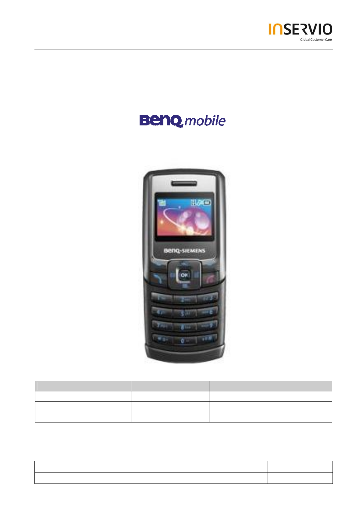
A38
Release Date Department Notes to change
R 1.0 06.09.2006 BQY CC S CES New document
Technical Documentation Release 1.0
TD_Repair_L3 _Theory of Operation_S38_R1.0.pdf Page 1 of 59
Created by inservio GmbH for BenQ mobile GmbH & Co. OHG - Company Confidential2006©inservio
Page 2

Table of Content
1 Introduction ...............................................................................................................................4
1.1 PURPOSE ...............................................................................................................................4
1.2 SCOPE ...................................................................................................................................4
2 List of available level 3 parts....................................................................................................5
3 Required Equipment for Level 3 ..............................................................................................7
4 Required Software for Level 3..................................................................................................7
5 PCB Main Board Overview .......................................................................................................8
6 Radio Part Introduction.............................................................................................................9
6.1 RECEIVER OPERATION..........................................................................................................10
6.2 TRANSMITTER OPERATION ....................................................................................................12
6.3 KEY COMPONENTS ...............................................................................................................14
6.3.1 T/R SWITCH ......................................................................................................................14
6.3.2 POWER AMPLIFIER ............................................................................................................14
6.3.3 TRANSCEIVER HD155165BP.............................................................................................15
6.3.4 SAW FILTER .....................................................................................................................15
7 Logic / Control Introduction...................................................................................................16
7.1 CALYPSO- BLOCK DIAGRAM (HERCROM200G2)..................................................................17
7.1.1 ARM MEGA-CELL (ARM7TDMIE) .....................................................................................20
7.1.2 DSP SUB-CHIP (S28C128) ...............................................................................................20
7.1.3 INTERNAL STATIC RAM .....................................................................................................20
7.1.4 INTERNAL BOOT ROM ........................................................................................................21
7.1.5 MEMORY INTERFACE .........................................................................................................22
7.1.6 MEMORY PROTECTION UNIT (MPU)...................................................................................22
7.1.7 DEBUG UNIT (DU) .............................................................................................................22
7.1.8 INTERRUPT HANDLER (INTH).............................................................................................22
7.1.9 TIMERS .............................................................................................................................23
7.1.10 ARM I/O ...........................................................................................................................23
7.1.11 UART-MODEM & UART-IRDA ..........................................................................................24
7.1.12 MICRO WIRE INTERFACE (U- WIRE) ....................................................................................24
7.1.13 MASTER I2C SERIAL INTERFACE ........................................................................................24
7.1.14 SERIAL PROT INTERFACE (SPI)..........................................................................................24
7.1.15 SUBSCRIBER IDENTITY MODULE (SIM) ...............................................................................25
7.1.16 REAL TIME CLOCK (RTC) ..................................................................................................25
Technical Documentation Release 1.0
TD_Repair_L3 _Theory of Operation_S38_R1.0.pdf Page 2 of 59
Created by inservio GmbH for BenQ mobile GmbH & Co. OHG - Company Confidential2006©inservio
Page 3

7.1.17 ULTRA LOW POWER DEVICE (ULPD) .................................................................................26
7.1.18 JOINED TEST ACTION GROUP (JTAG)................................................................................26
7.1.19 CIPHERING PROCESSOR (CRYPT) ....................................................................................26
7.1.20 RADIO INTERFACE (RIF) ....................................................................................................26
7.1.21 MULTI-CHANNEL SERIAL INTERFACE (MCSI) ......................................................................27
7.1.22 PULSE WIDTH TONES (PWT).............................................................................................27
7.1.23 PULSE WIDTH LIGHT (PWL)...............................................................................................27
7.2 IOTA (TWL3025).................................................................................................................28
7.2.1 INTRODUCTION OF IOTA....................................................................................................28
7.2.2 BLOCK SPECIFICATIONS (IOTA) ..................................................................................28
7.2.3 USP (MCU SERIAL PORT).................................................................................................30
7.2.4 BSP (BASE BAND SERIAL PORT)........................................................................................30
7.2.5 BBC (BASE BAND CODEC) ................................................................................................31
7.2.6 BDL (BASE BAND DOWNLINK PATH) ....................................................................................31
7.2.7 AFC & APC ......................................................................................................................32
7.2.8 VREG (VOLTAGE REGULATION).........................................................................................34
7.2.9 VRPC (VOLTAGE REFERENCE POWER CONTROL) ..............................................................34
7.2.10 BCI (BATTERY CHARGER INTERFACE)................................................................................35
7.2.11 VBC (VOICE BAND CODEC)................................................................................................36
7.2.12 TSP (TIME SERIAL PORT)..................................................................................................37
7.2.13 SIM CARD INTERFACE (SIM) .............................................................................................37
7.2.14 AUXILIARY CURRENT DRIVER (ACD) ..................................................................................38
7.2.15 AUXILIARY DAC (ADAC) ...................................................................................................38
7.3 INTRODUCTION TO MEMORY DEVICES ...................................................................................39
7.4 INTRODUCTION TO EXTERNAL PERIPHERY CIRCUITS ...............................................................40
7.4.1 MELODY LSI .....................................................................................................................40
7.4.2 VIBRATING MOTOR ............................................................................................................41
7.4.3 KEYBOARD LED CIRCUIT ...................................................................................................42
7.4.4 KEYBOARD CIRCUIT ...........................................................................................................43
7.4.5 AUDIO CIRCUIT ..................................................................................................................44
7.4.6 AUDIO JACK CIRCUIT .........................................................................................................46
7.4.7 SIM READER CIRCUIT .......................................................................................................47
7.4.8 DISPLAY CIRCUITS .............................................................................................................47
7.4.9 CHARGING CIRCUIT............................................................................................................48
Appendix A: Charging Algorithm................................................................................................50
Technical Documentation Release 1.0
TD_Repair_L3 _Theory of Operation_S38_R1.0.pdf Page 3 of 59
Created by inservio GmbH for BenQ mobile GmbH & Co. OHG - Company Confidential2006©inservio
Page 4

1 Introduction
1.1 Purpose
This Service Repair Documentation is intended to carry out repairs on BenQ repair level 3.
1.2 Scope
This document is the reference document for all BenQ authorised Service Partners which are
released to repair BenQ Siemens Mobile phones up to level 3.
Technical Documentation Release 1.0
TD_Repair_L3 _Theory of Operation_S38_R1.0.pdf Page 4 of 59
Created by inservio GmbH for BenQ mobile GmbH & Co. OHG - Company Confidential2006©inservio
Page 5
2 List of available level 3 parts
Product Chipset ID OrderNumber DescriptionCM
A38 TI ANT1 L50634-Z97-C554 CONN ANT 5.1*3*5 RF05301-PG
A38 TI ANT2 L50634-Z97-C554 CONN ANT 5.1*3*5 RF05301-PG
A38 TI BQ250 L50640-C2143-D670 XTOR BC807-40W SOT-323 PNP
A38 TI BQ350 L50640-C2150-D670 XTOR UMT4403 UMT3 PNP
A38 TI C653 L50695-F3157-M1 CHIP CAP T 150UF 10V M7132
A38 TI D250 L50640-D5111-D670 Diode SB CRS03 30V1A PMDU
A38 TI D350 L50640-L2180-D670 LED BLUE 0603M BL-HB536G-TRB
A38 TI D351 L50640-L2180-D670 LED BLUE 0603M BL-HB536G-TRB
A38 TI D352 L50640-L2180-D670 LED BLUE 0603M BL-HB536G-TRB
A38 TI D353 L50640-L2180-D670 LED BLUE 0603M BL-HB536G-TRB
A38 TI D354 L50640-L2180-D670 LED BLUE 0603M BL-HB536G-TRB
A38 TI D355 L50640-L2180-D670 LED BLUE 0603M BL-HB536G-TRB
A38 TI D356 L50640-D5110-D670 Diode SB 0.2A30V RB520S-30
A38 TI D357 L50640-D5110-D670 Diode SB 0.2A30V RB520S-30
A38 TI DZ250 L50640-D3142-D670 Diode ZEN 6.06-6.33V 200MW UMD
A38 TI EN150 L50645-K280-Y427 FILTER EMI 1GHZ CSPEMI202AG
A38 TI F250 L50645-A820-Y47 CHIP FUSE 1A 32V F0603 TR/0603
A38 TI J250 L50634-Z97-C553 JACK DC PWR PA05302-QNJ
A38 TI J300 L50634-Z97-C679 CONN SPK3.1N2P 6.2*4.8*1PT/ASP
A38 TI J450 L50634-Z97-C558 CONN I/O 10P P0.5 215+916+2941
A38 TI JP250 L50634-Z97-C556 CONN BATT 3P D2.5 AB303Y-C0G1G
A38 TI LCD L50651-Z1508-A197 LCDM WD-X0906XE-6CLWB
A38 TI Q1 L50640-C4086-D670 XTOR 2SC5658T2LR VMT3 NPN
A38 TI R604 L50645-K260-Y110 CHIP ATTENUATOR 3DB PAT1010-X
A38 TI RN350 L50653-F4221-J CHIP NTW 220 J 8P 2*1*0.4
A38 TI RN351 L50653-F4221-J CHIP NTW 220 J 8P 2*1*0.4
A38 TI U100 L50645-J4683-Y31 IC ASIC D751749ZHHR BGA 179P
A38 TI U150 L50610-U6243-D670 IC INTF TWL3025BZGMR PBGA 100P
A38 TI U151 L50634-Z97-C713 CONN SIM CARD 6P BM05306-J7G
A38 TI U200 L50610-F6504-D670 IC FLASH S29PL032J70BFI BQ7B.29032.B3U
A38 TI U201 L50610-F6505-D670 IC SRAM SV5P4016UFA-70P BQ7B.54016.03U
A38 TI U250 L50640-C2168-D670 XTOR DTC144EET1G SC-75 NPN
A38 TI U251 L50630-C1187-D670 FET MOS FDC6506P SOT-6 PC
A38 TI U252 L50610-C6126-D670 IC DETECTOR XC61CC4402N SSOT24
A38 TI U253 L50640-C2144-D670 XTOR DTC143ZET1G SC-75 NPN
A38 TI U325 L50610-U6282-D670 IC DC/DC CONV RT9361APE SOT-26
A38 TI U350 L50640-C2144-D670 XTOR DTC143ZET1G SC-75 NPN
A38 TI U400 L50610-C6430-D670 IC POLY AUDIO SPMA120A-EV083
A38 TI U451 L50645-K280-Y423 FILTER 800-2700MHZ CSPEMI204G
A38 TI U452 L50640-C2149-D670 XTOR PEMH9 NPN SOT666 6P
A38 TI U602 L50610-U6244-D670 IC IR XCVR HD155165BPEB BGA
A38 TI U603 L50645-K280-Y428 FILTER RF SAW 942.5MHZ B9017
A38 TI U604 L50645-K280-Y429 FILTER SAW 1842.5/1960M SAWEP1
Technical Documentation Release 1.0
TD_Repair_L3 _Theory of Operation_S38_R1.0.pdf Page 5 of 59
Created by inservio GmbH for BenQ mobile GmbH & Co. OHG - Company Confidential2006©inservio
Page 6
A38 TI U606 L50610-U6247-D670 IC PWR AMP RF3166-E6 SMD
A38 TI U608 L50610-B6218-D670 IC DUAL BUFFER NC7WZ16 SC70-6P
A38 TI U609 L50610-U6248-D670 IC SWITCHPLEXER LMSP54CA-272
A38 TI U610 L50645-F102-Y48 XTAL 26MHZ 10PF 8PPM U-860-1-1
A38 TI U611 L50610-C6289-D670 IC VR MAS9124A2GC06 TSOT-5
A38 TI U72 L50615-Z77-C287 SW RF ANTENNA MS-147 HIROSE
A38 TI X100 L50645-F102-Y49 XTAL 32.768K12.5PF20PPM DST520
A38 TI X150 L50634-Z97-C559 CONN MIC 2P TRA21-2K8 56F55
Technical Documentation Release 1.0
TD_Repair_L3 _Theory of Operation_S38_R1.0.pdf Page 6 of 59
Created by inservio GmbH for BenQ mobile GmbH & Co. OHG - Company Confidential2006©inservio
Page 7

3 Required Equipment for Level 3
GSM-Tester (CMU200 or 4400S incl. Options)
PC-incl. Monitor, Keyboard and Mouse
Power Supply
Board Adapter A38
Spectrum Analyser
Active RF-Probe incl. Power Supply
Oscilloscope incl. Probe
Power Supply Cables
BGA Soldering equipment
Reference: Equipment recommendation V1.6
(Downloadable from the technical support page)
4 Required Software for Level 3
Windows XP
BenQ Troubleshooting Software XCSD Level2
Technical Documentation Release 1.0
TD_Repair_L3 _Theory of Operation_S38_R1.0.pdf Page 7 of 59
Created by inservio GmbH for BenQ mobile GmbH & Co. OHG - Company Confidential2006©inservio
Page 8
r
g
A
r
A
p
y
A
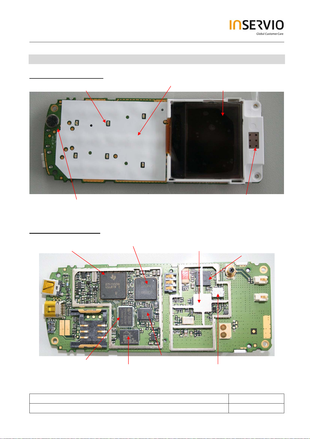
5 PCB Main Board Overview
PCB Main Board Back Side
LED
Metal Dome Film LCD Module
PCB Main Board Top Side
Microphone
G2
IOT
Loudspeake
Transceiver (under
shieldin
frame)
Power Amplifie
SRAM
Technical Documentation Release 1.0
TD_Repair_L3 _Theory of Operation_S38_R1.0.pdf Page 8 of 59
Created by inservio GmbH for BenQ mobile GmbH & Co. OHG - Company Confidential2006©inservio
Flash Memor
udio Chi
ntenna Switch
Page 9
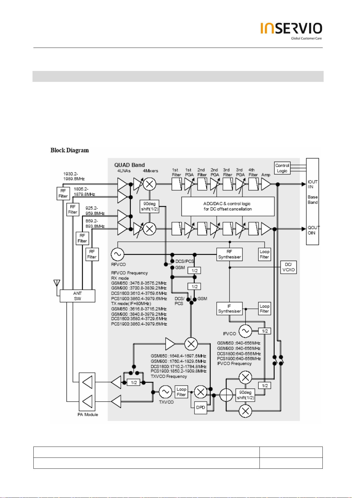
6 Radio Part Introduction
T he following session elaborates the basic functionalities of RF-related chip sets: HD155165BP
(Transceiver, Synthesizer and Universal Baseband Interface). Those will give readers
fundamental concept about how they work.
Technical Documentation Release 1.0
TD_Repair_L3 _Theory of Operation_S38_R1.0.pdf Page 9 of 59
Created by inservio GmbH for BenQ mobile GmbH & Co. OHG - Company Confidential2006©inservio
Page 10

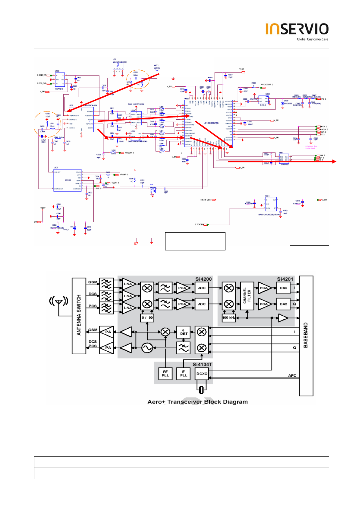
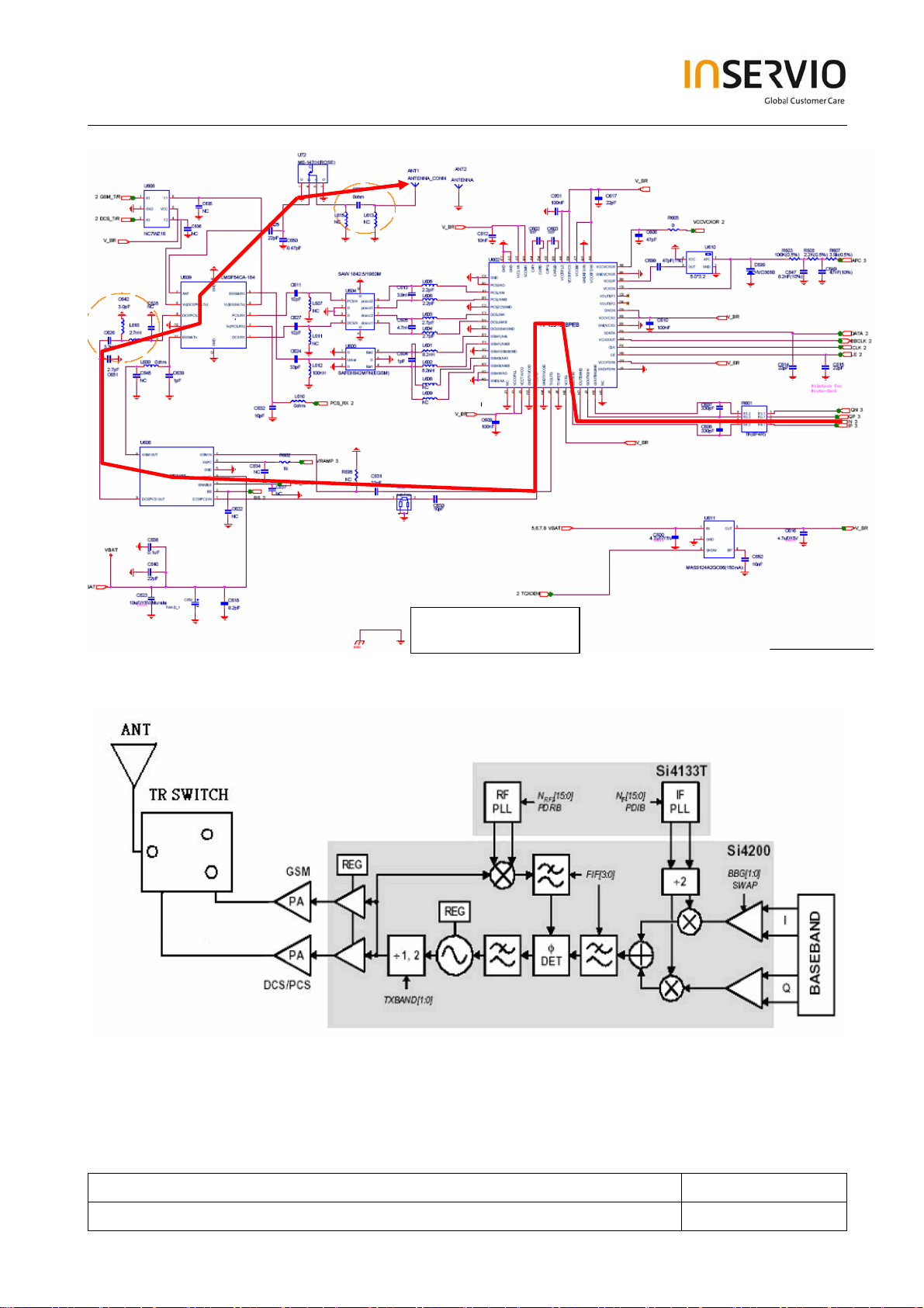
6.1 Receiver Operation
The Aero+ transceiver uses a low-IF receiver architecture that allows for the on-chip integration of
the channel selection filters.
The Si4200 integrates three differential-input LNAs. The LNA amplifies the RF signal after selection
by the T/R switch and RF SAW filter before the signal enters the first mixer section. The LNA inputs
are matched to the 200Ω balanced output SAW filters through external LC matching networks.
A mixer down converts the RF signal to a 100 kHz intermediate frequency (IF) with the RFLO from
the Si4134T frequency synthesizer. The RFLO frequency is between 1737.8 and 1989.9 MHz, and
is divided by two in the Si4200 for GSM850 and EGSM 900 modes. The mixer output is amplified
with an analog programmable gain amplifier (PGA), which dynamic range is 16 dB and gain step is 4
dB.
The quadrature IF signal is digitized with high-resolution A/D converters (ADCs). The Si4201 down
converts the ADC output to base band with a digital 100 kHz quadrature LO signal. The digital
output is scaled with a digital PGA, which dynamic range is 63 dB and gain step is 1 dB. DACs drive
a differential analog signal onto the RXIP, RXIN, RXQP and RXQN pins to interface to standard
analog-input base band ICs.
Technical Documentation Release 1.0
TD_Repair_L3 _Theory of Operation_S38_R1.0.pdf Page 10 of 59
Created by inservio GmbH for BenQ mobile GmbH & Co. OHG - Company Confidential2006©inservio
Page 11
Antenna
IOTA
Receiver Path
Technical Documentation Release 1.0
TD_Repair_L3 _Theory of Operation_S38_R1.0.pdf Page 11 of 59
Created by inservio GmbH for BenQ mobile GmbH & Co. OHG - Company Confidential2006©inservio
Page 12

6.2 Transmitter Operation
The transmitter chain converts differential IQ base band signals to a suitable format for transmission
by a power amplifier.
The transmit (TX) section consists of an I/Q base band up converter, an offset phase-locked loop
(OPLL) and two 50 Ω output buffers that can drive external power amplifiers (PA), one for the EGSM
and one for the DCS 1800 and PCS 1900 band. A quadrature mixer up converts the differential in-
phase (TXIP, TXIN) and quadrature (TXQP, TXQN) signals with the IFLO to generate an IF signal
which is filtered and used as the reference input to the OPLL. The Si4134T generates the IFLO
frequency between 766 and 896 MHz. The IFLO is divided by two to generate the quadrature LO
signals for the quadrature modulator, resulting in an IF between 383 and 448 MHz.
The OPLL consists of a feedback mixer, a phase detector, a loop filter, and a fully integrated
TXVCO. The TXVCO centres between the DCS 1800 and PCS 1900 bands, and its output is divided
by two for the GSM850 and E-GSM 900 bands. The Si4134T generates the RFLO frequency
between 1272 and 1483 MHz. To allow a single VCO to be used for the RFLO, high-side injection is
used for the E-GSM 900 bands, and low-side injection is used for the DCS 1800 and PCS 1900
bands.
The RF signal is then amplified by PA (RFMD3140) and power control loop to the assigned power
level within the burst.
Technical Documentation Release 1.0
TD_Repair_L3 _Theory of Operation_S38_R1.0.pdf Page 12 of 59
Created by inservio GmbH for BenQ mobile GmbH & Co. OHG - Company Confidential2006©inservio
Page 13
Antenna
IOTA
Transmitter Path
Technical Documentation Release 1.0
TD_Repair_L3 _Theory of Operation_S38_R1.0.pdf Page 13 of 59
Created by inservio GmbH for BenQ mobile GmbH & Co. OHG - Company Confidential2006©inservio
Page 14
6.3 Key Components
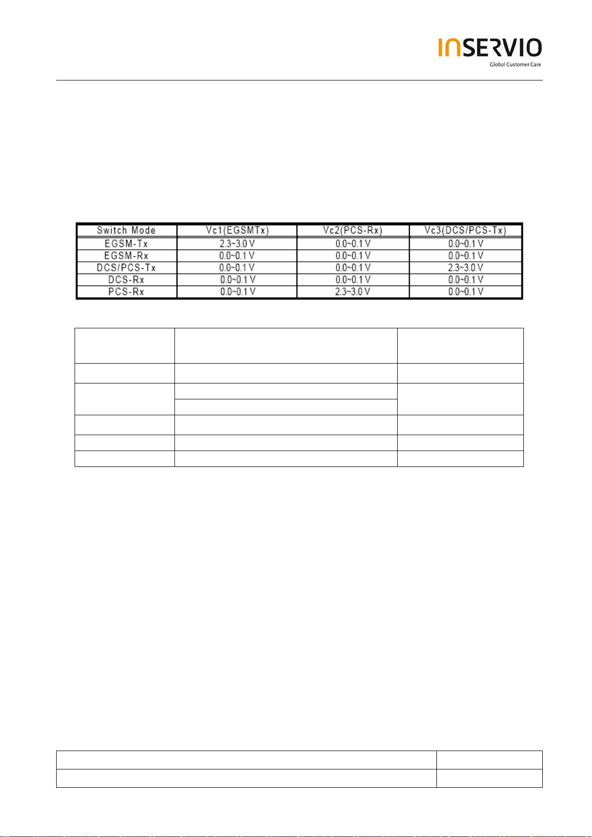
6.3.1 T/R Switch
TRS201 is a front-end switch device for EGSM/DCS/PCS. The following Table 3-1 shows the
required pin-voltage combinations for each operating modes
Table 6-1
Table 6-2
Mode
Frequency Range (MHz)
Insertion Loss @25℃
(dB)
EGSM TX
DCS/PCS TX
897.5±17.5
1747.5±37.5 (DCS)
1.3 max
1.25 max
1880.0±30.0 (PCS)
EGSM RX
DCS RX
PCS RX
942.5±17.5
1842.5±37.5
1960.0±30.0
1.0 max
1.2 max
1.55 max
6.3.2 Power Amplifier
The PA, which integrates the power level control circuit, is controlled by signal BSW, PCLON and
RAMP. The purpose of the BSW is for band- select control. The RAMP signal is for power level
control. The PCLON signal is for power saving control. As the supply requirements, the supply
voltage is 3.6V and the control loop required voltage is 2.8V.
The following formula provides the required ramping voltage at the flat portion of bursts:
Vramp= 0.12+SF*0.002 (V), where SF: Scaling Factor
Technical Documentation Release 1.0
TD_Repair_L3 _Theory of Operation_S38_R1.0.pdf Page 14 of 59
Created by inservio GmbH for BenQ mobile GmbH & Co. OHG - Company Confidential2006©inservio
Page 15
6.3.3 Transceiver HD155165BP
The HD155165BP is a highly integrated RF transceiver IC for GSM850, GSM900, DCS1800and
PCS1900 quad-band cellular systems. The HD155165BP incorporates four RF low-noise amplifiers,
direct conversion mixers, a programmable gain amplifier with multistage filtering and DC offset
correction, fully integrated VCOs, RF/IF synthesizers, and a low-noise offset PLL transmitter. The
HD155165BP includes state machine control serial programming. All functions operate down to 2.7V
and are housed in a 57-pin BGA package. Hence the HD155165BP can form a small size
transceiver handset for quad band.
6.3.4 SAW Filter
The BPF201, BPF202 and BPF203 are the front-end filtering device on receiving path, for GSM,
DCS and PCS bands, respectively. They also provide mode conversion mechanism (unbalance to
balance).
Table 3-3 shows the worse case insertion loss for Epcos filters.
Table 6-3
Mode Frequency Range (MHz)
EGSM 925~960 2.1 max
DCS 1805~1880 2.1 max
PCS 1930~1990 2.4 max
Insertion Loss @25℃ (dB)
Technical Documentation Release 1.0
TD_Repair_L3 _Theory of Operation_S38_R1.0.pdf Page 15 of 59
Created by inservio GmbH for BenQ mobile GmbH & Co. OHG - Company Confidential2006©inservio
Page 16

7 Logic / Control Introduction
A38 consists of GSM chipsets --ABB, DBB, PA, transceiver, filters and plenty of peripheries. They
can provide wireless communication solutions for any products that have requirements of voice/data
transmission, particularly portable devices or handheld equipments.
In addition, A38 integrates other peripheries such as polyphony chip that plays melodies, display
with 65K-color C-STN LCD, LEDs for keypads, vibrating motor, memory device and charging etc.
The baseband part consists of TI’s GSM digital signal processor (Calypso-) with the micro-controller
unit and TI’s analog device (IOTA) that performs the interface and processing of voice signals,
interface and processing of base band in-phase (I) and quadrature (Q) signals. Moreover, the base
band part includes a flash device used for software program code and a SRAM for software program
execution.
Baseband provides functions like UART, GPIO, voice, SIM, keypads, memory interface, low dropout
regulator and synchronous clock to the peripheral chip for timing reference…etc. These features can
certainly meet most customers’ design requirement and simplify the developing process for a variety
of portable devices
In the following sections, we’ll give the detailed descriptions for each baseband chip component, and
then we’d continue to emphasize the introductions to the specific periphery circuits that interface.
Technical Documentation Release 1.0
TD_Repair_L3 _Theory of Operation_S38_R1.0.pdf Page 16 of 59
Created by inservio GmbH for BenQ mobile GmbH & Co. OHG - Company Confidential2006©inservio
Page 17

7.1 Calypso- Block Diagram (HERCROM200G2)
CALYPSO Lite architecture is based on two processor cores ARM7 & LEAD2 using the generic TI
RHEA bus standard as interface with their associated application peripherals.
This CALYPSO lite is composed from the following blocks:
• ARM7TDMIE (32/16 bits RISC processor)
- ARM “Ice Crusher” for emulation purpose.
• LEAD2 DSP core with 28K words of RAM and 128K words of ROM
- Associated with API, SPI, and TIMER.
• Clock squarer cell.
• ARM general-purpose peripherals:
- ARM Memory Interface (MEMIF) for external RAM, Flash or ROM.
- RHEA Bridge.
- 4M bits SRAM with write-buffer.
- Memory Protection Unit (MPU).
- Debug Unit (DU).
- 64k bits ROM for internal boot.
- Die-ID cell.
• ARM application peripherals:
- ARM I/O.
- Micro Wire Interface.
- 3 Timers.
Technical Documentation Release 1.0
TD_Repair_L3 _Theory of Operation_S38_R1.0.pdf Page 17 of 59
Created by inservio GmbH for BenQ mobile GmbH & Co. OHG - Company Confidential2006©inservio
Page 18

- UART_IRDA & UART_MODEM.
- SIM Interface.
- Interrupt Handler (INTH).
- Time Processing Unit (TPU).
- Time Serial Port (TSP).
- Direct Memory Access (DMA).
- Real Time Clock (RTC).
- Ultra Low-Power Device (ULPD).
- Clock Management (CLKM).
- Light Pulse Generator (LPG), Pulse Width Tone (PWT), Pulse Width Light (PWL).
- Master I2C serial Interface
- GPRS Encryption Algorithm Module 1 & 2.
• ASIC DSP general-purpose peripherals:
- RHEA Bridge.
• DSP application peripherals.
- Radio Interface (RIF).
- Multi-Channel Serial Port (MCSI).
- Ciphering Processor (CRYPT).
- Direct Memory Access (DMA).
- DSP Interrupt Handler (INTH).
- UART Interface.
Technical Documentation Release 1.0
TD_Repair_L3 _Theory of Operation_S38_R1.0.pdf Page 18 of 59
Created by inservio GmbH for BenQ mobile GmbH & Co. OHG - Company Confidential2006©inservio
Page 19

• Other ASIC peripheral:
- JTAG TAP controller
Technical Documentation Release 1.0
TD_Repair_L3 _Theory of Operation_S38_R1.0.pdf Page 19 of 59
Created by inservio GmbH for BenQ mobile GmbH & Co. OHG - Company Confidential2006©inservio
Page 20

Calypso- Block Specification (HERCROM200G2
)
7.1.1 ARM Mega-Cell (ARM7TDMIE)
The ARM7TDMI is a 32 bits RISC micro-controller core. This microprocessor work in 32/16 bits
instructions, and 32/16/8 bits data. The input clock frequency is 13/26MHz. The functional cycle
frequency is planned by CLKM.
Single processor and multiprocessor debug
High level language and assembly debug
Real time or non real time debugs options
Combined 32/16-bit mode for ARM processor
Endianess transparency
Unlimited breakpoints via op-code replacement (SW breakpoint)
2 HW breakpoints with maskable cycle type, address and data compare
2 external breakpoint events
Internal events generate external triggers
Benchmarking / profiling capability
7.1.2 DSP Sub-Chip (S28C128)
This DSP sub-chip is a Digital Signal Processor core compliant with the TMS320C54x family.
The input clock frequency is 13/26MHz.
The input clock frequency is delivered by a DPLL.
The functional cycle frequency is planned to be in the range [0~91] MHz
7.1.3 Internal Static RAM
A 4M bits SRAM (Static Random Access Memory) are embedded on the die and mapped on nCS6
chip-select signal.
Technical Documentation Release 1.0
TD_Repair_L3 _Theory of Operation_S38_R1.0.pdf Page 20 of 59
Created by inservio GmbH for BenQ mobile GmbH & Co. OHG - Company Confidential2006©inservio
Page 21

Memory range [0080:0000 ~ 00BF: FFFF].
The memory can be read or written either in 8/16/32 bits format.
SRAM 2Mb
2M-bit Internal SRAM
7.1.4 Internal Boot Rom
An 8K bytes ROM (Read Only Memory) is embedded and mapped on nCS7 chip-select of the
memory interface.
Memory range [0000:0000 ~ 0000:1FFF].
The memory can be read in 8/16/32
bits format.
If the nIBOOT signal is equal to ‘0’, the Boot ROM is
allocated on memory address 0000:0000 ~
0000:1FFF.
8K-byte Boot ROM
Technical Documentation Release 1.0
TD_Repair_L3 _Theory of Operation_S38_R1.0.pdf Page 21 of 59
Created by inservio GmbH for BenQ mobile GmbH & Co. OHG - Company Confidential2006©inservio
Page 22

7.1.5 Memory Interface
Memory Interface: using ADD (22)
7.1.6 Memory Protection Unit (MPU)
Within a memory space, the MPU allows defining memory sub regions, each having a separate
Read/Write protection attribute. This permits for partitioning the memory space into program
instruction, system data, and user data, stack…
7.1.7 Debug Unit (DU)
The Debug Unit is a hardware resource intended to provide additional support to software abort-
handler. The DU provides 64 stages deep history table of the last memory accesses prior entering
the abort mode, and then permitting analysis of previous bus transactions.
7.1.8 Interrupt Handler (INTH)
The interrupt handler is a module that shares two ARM interrupts (FIQ, IRQ) between several
possible sources.
The interrupt handler provides up to 21 interrupts.
All interrupts:
can be edge or level sensitive.
Technical Documentation Release 1.0
TD_Repair_L3 _Theory of Operation_S38_R1.0.pdf Page 22 of 59
Created by inservio GmbH for BenQ mobile GmbH & Co. OHG - Company Confidential2006©inservio
Page 23

can have different priorities.
can be individually masked.
If several interrupts have the same priority level, they are sent in a predefined order.
Original priority -> IRQ_N-1, IRQ_N-2, IRQ_0 (N=21).
7.1.9 Timers
This chip implements three 16-bits Timers (A Watchdog and two General Purpose Timers). These
Timers generate interrupts to ARM when Timer is equal to zero.
General Purpose Timer
Auto-reload and one-shot function.
Watchdog Timer: The watchdog is designed to detect user programs stuck in infinite
loops resulting in loss of program control or “runaway” programs.
7.1.10 ARM I/O
ARMI/O consists of:
16 general-purpose I/O pins.
10 special I/O pins are dedicated for keyboard connection: 5 output (column) x 5
input (row).
special I/O pins are dedicated for buzzer & light control.
general purpose I/O pins can be configured as input or output pin.
light and buzzer are controlled by PWM.
Two registers are used to define power level:
Light level register: 6 bit and allow to program up to 64 levels.
Buzzer level register: 6 bit and allow to program up to 64 levels.
Technical Documentation Release 1.0
TD_Repair_L3 _Theory of Operation_S38_R1.0.pdf Page 23 of 59
Created by inservio GmbH for BenQ mobile GmbH & Co. OHG - Company Confidential2006©inservio
Page 24

7.1.11 UART-Modem & UART-IRDA
UART-Modem
This UART interface is compatible with 16C750 device. It is devoted to connection to a Modem
through a standard wired interface. Auto-Baud Rate is from 1200 to 115.2K bits/sec.
UART-IRDA
This UART Interface is compatible with 16C750 device. It includes the Slow Infra-Red protocol (SIR)
encoder/decoder in order to be connected with an infrared transmitter to any external data
peripheral with an IRDA data interface. Baud-rate from 75 to 115.2K bits/sec.
7.1.12 Micro Wire Interface (u- Wire)
This Micro-Wire interface can drive 2 serial external components as EEPROM or LCD. 2 chips
selects signal: nSCS0, nSCS1 can be used. The Micro-Wire is a full-duplex serial port using 3 lines
(SDI: Data-in and SDO: Data-out and SCLK: Clock) for data transmission. The serial clock period is
derived from the reference 13MHz clock and can be configured as:
- TSCLK=CK_FREQ * CSI_FRQ * T13M=[2/4/7/10] * [2/4/8] * T13M
7.1.13 Master I2C Serial Interface
The I2C is a half-duplex serial port using 2 lines (SDA: Data and SCL: Clock) for data transmission
with software addressable external devices.
The main feature of I2C Master: Single master only.
Standard (100KHz: SCL clock frequency) and fast (400KHz: SCL clock frequency) transmission
modes.
7.1.14 Serial Prot Interface (SPI)
The SPI is a full-duplex serial port. The SPI provides 3 enable signals: MCUEN0, MCUEN1,
MCUEN2.
The SPI is using 3 lines (MCUEN0: Enable, MCUDI: Input serial data, MCUDO: Output serial
data) for data transmission through Serial port on Analog Base-Band.
Technical Documentation Release 1.0
TD_Repair_L3 _Theory of Operation_S38_R1.0.pdf Page 24 of 59
Created by inservio GmbH for BenQ mobile GmbH & Co. OHG - Company Confidential2006©inservio
Page 25

7.1.15 Subscriber Identity Module (SIM)
The SIM interface module ensures the interoperability between a Subscriber Identity Module and the
Micro-controller in charge of the GSM layer-3 protocol related to the SIM management.
It Interface with:
The SIM card through SIM level shifter module on ABB.
The MCU through RHEA bus.
7.1.16 Real Time Clock (RTC)
The RTC block is an embedded Real Time Clock module, directly accessible from RHEA bus
interface.
Its basic functionality:
Time information (seconds/minutes/hours) directly in BCD code.
Calendar Information (Day/Month/Year) directly in BCD code up to year 2099.
Alarm function with interrupts generation based on a periodical (second/minute/hour/day)
or a precise time event in the century
Technical Documentation Release 1.0
TD_Repair_L3 _Theory of Operation_S38_R1.0.pdf Page 25 of 59
Created by inservio GmbH for BenQ mobile GmbH & Co. OHG - Company Confidential2006©inservio
Page 26

32K Hz oscillator frequency calibration.
30s time range correction
7.1.17 Ultra Low Power Device (ULPD)
The ULPD block is used for the Deep Sleep Mode management.
The Deep Sleep Mode is characterized by the freeze of all the clocks in chip that derived from the
3MHz reference clock, thus authorizing to stop the external VTCXO clock source.
The sleeping period is monitored with a timer based on a low frequency 32 KHz clock, which will be
used to maintain the GSM time base with minimum required accuracy.
The main functions of ULPD blocks:
Maintenance of GSM time during deep sleep mode with minimum time accuracy.
Programmable timer to exit deep sleep mode.
Switching between 13MHz and 32 KHz.
Generation of chip functional reset.
7.1.18 Joined Test Action Group (JTAG)
The JTAG Interface of the chip can be selected either to access the 2 processors on-chip emulators
with a pseudo IEEE JTAG protocol for emulation purpose or to dialog with an embedded TAP
controller which instructions set support all the IEEE 1149.1 BSCAN.
7.1.19 Ciphering Processor (CRYPT)
This CRYPT module implements the functionality of the ciphering algorithms A51 and A52. The
ciphering takes place before modulation and the deciphering takes place after demodulation.
7.1.20 Radio Interface (RIF)
The RIF (Radio Interface) Module is a buffered serial port derived from the BSP peripheral module.
The external serial data transmission is a full-duplex interface (BFSR: Receive synchronization,
BDR: Receive data, BFSX: Transmit synchronization, BDX: Transmit data).
Technical Documentation Release 1.0
TD_Repair_L3 _Theory of Operation_S38_R1.0.pdf Page 26 of 59
Created by inservio GmbH for BenQ mobile GmbH & Co. OHG - Company Confidential2006©inservio
Page 27

7.1.21 Multi-Channel Serial Interface (MCSI)
The MCSI is a serial interface with multi-channels (x16) transmission capability.
The interface supports GSM DAI (Digital Audio Interface) operating modes (Radio uplink, Radio
downlink, acoustic).
In DAI mode, the MCSI interface is configured to be directly connected to the GSM System
Simulator interface.
7.1.22 Pulse Width Tones (PWT)
This module generates a modulated frequency signal for the external buzzer. Frequency is
programmable from 349Hz to 5276Hz (FRC). The volume is also programmable (VRC).
7.1.23 Pulse Width Light (PWL)
It allows the control of backlight of LCD and keypad.
Technical Documentation Release 1.0
TD_Repair_L3 _Theory of Operation_S38_R1.0.pdf Page 27 of 59
Created by inservio GmbH for BenQ mobile GmbH & Co. OHG - Company Confidential2006©inservio
Page 28

7.2 IOTA (TWL3025)
7.2.1 Introduction of IOTA
IOTA General Description
Analog base band device
Interface and processing of voice signals
Interface and processing of base band in-phase (I) and quadrature (Q) signals
Supply voltage regulation
Battery charging control
IOTA Features
Applications include GSM900, DCS 1800, and andPCS1900 cellular phone.
Voice coder/decoder (codec)
Base band codec single/multi-slot with I/Q RF interface
Auxiliary RF CONV.
SIM card interface
Li-ion or Ni-MH battery charging control
Six LDOs linear voltage regulators
Dedicated low quiescent current mode on regulators
Voltage detectors
Four-channel analog-to-digital CONV.
Dedicated very low quiescent current domain supply
7.2.2 BLOCK SPECIFICATIONS (IOTA)
IOTA Block Diagram
Technical Documentation Release 1.0
TD_Repair_L3 _Theory of Operation_S38_R1.0.pdf Page 28 of 59
Created by inservio GmbH for BenQ mobile GmbH & Co. OHG - Company Confidential2006©inservio
Page 29

Technical Documentation Release 1.0
TD_Repair_L3 _Theory of Operation_S38_R1.0.pdf Page 29 of 59
Created by inservio GmbH for BenQ mobile GmbH & Co. OHG - Company Confidential2006©inservio
Page 30

S
7.2.3 USP (MCU Serial Port)
Communicate with the micro controller core
UEN
UEN: Port enable
MCU
UDR: Data receive
UDX: Data transmit
CK13M master clock.
7.2.4 BSP (Base band Serial Port)
BFSR: BSP receive frame synchronization
BDR: BSP receive data
BFSX: BSP transmit frame synchronization
UDR
UDX
BFSR
BDR
BF
BDX
Serial port
Baseband
X
Serial port
BDX: BSP transmit data
Technical Documentation Release 1.0
TD_Repair_L3 _Theory of Operation_S38_R1.0.pdf Page 30 of 59
Created by inservio GmbH for BenQ mobile GmbH & Co. OHG - Company Confidential2006©inservio
Page 31

7.2.5 BBC (Base Band Codec)
BUL (base band uplink path)BULIP, BULIM, BULQP, BULQM
7.2.6 BDL (base band downlink path)
Technical Documentation Release 1.0
TD_Repair_L3 _Theory of Operation_S38_R1.0.pdf Page 31 of 59
Created by inservio GmbH for BenQ mobile GmbH & Co. OHG - Company Confidential2006©inservio
Page 32

7.2.7 AFC & APC
AFC
DAC optimized for high resolution DC conversion (13bits, 2.0 V).The GSM 13 MHz master clock
frequency in a 0.1-PPM range.
APC
P
ower ramping up, ramping down and power level of the radio burst.
i
ncludes a DAC and a RAM
S
mooth power transition
T
iming of the APC coming from the TSP
Technical Documentation Release 1.0
TD_Repair_L3 _Theory of Operation_S38_R1.0.pdf Page 32 of 59
Created by inservio GmbH for BenQ mobile GmbH & Co. OHG - Company Confidential2006©inservio
Page 33

MADC8 channel, 10-bit analog to digital converter
4 are remaining:
m
ain battery voltage
b
ack up battery voltage
c
harger voltage
c
harger current monitoring.4 are available externally:
E
x: Battery type, Battery temp, ACCID, temperature compensated
Technical Documentation Release 1.0
TD_Repair_L3 _Theory of Operation_S38_R1.0.pdf Page 33 of 59
Created by inservio GmbH for BenQ mobile GmbH & Co. OHG - Company Confidential2006©inservio
Page 34

7.2.8 VREG (Voltage Regulation)
Three operation modes for each LDO regulators (except for VRRTC):
•–ACTIVE mode: regulator is able to deliver its full power
S
LEEP mode: the output voltage is maintained with a very low power consumption but with a
low c
urrent capability
O
FF mode: the output voltage is not maintained and the power consumption is null.
7.2.9 VRPC (Voltage Reference Power control)
B
and gap for voltage reference
P
ower on Control
V
RPC state machine.
P
ower ON, Power OFF, Switch On, and Switch OFF sequences.
I
nterrupt handling
I
NT1: low battery voltageàemergency switch-off procedure.
I
NT2: Charger is plugged or unplugged.
User pushes ON button (to activate a switch off) falling edge after debouncing on RPWON terminal.
Technical Documentation Release 1.0
TD_Repair_L3 _Theory of Operation_S38_R1.0.pdf Page 34 of 59
Created by inservio GmbH for BenQ mobile GmbH & Co. OHG - Company Confidential2006©inservio
Page 35

The MADC end-of-conversion interrupt.
7.2.10 BCI (Battery Charger Interface)
1
–cell Li–Ion battery or 3–series Ni–MH/Ni–Cd cell battery
T
he battery is monitored using the 10–bit AD charger voltage
-
charger current monitoring Auxiliary functions
-
Battery pre-charge,
-
Back–up battery charge,
Technical Documentation Release 1.0
TD_Repair_L3 _Theory of Operation_S38_R1.0.pdf Page 35 of 59
Created by inservio GmbH for BenQ mobile GmbH & Co. OHG - Company Confidential2006©inservio
Page 36

7.2.11 VBC (Voice band Codec)
Voice Uplink path (VUL)
Voice Downlink path (VDL)
Technical Documentation Release 1.0
TD_Repair_L3 _Theory of Operation_S38_R1.0.pdf Page 36 of 59
Created by inservio GmbH for BenQ mobile GmbH & Co. OHG - Company Confidential2006©inservio
Page 37

7.2.12 TSP (Time Serial Port)
-
Communicate with the TPU for real time control.
-
The above real-time control signals are processed by TPU within DBB.
-
TEN: enable.
-
TDR: data-receive.
-
The CL13M master clock divided by 2 is used internally as the clock for this serial port.
7.2.13 SIM Card Interface (SIM)
It is a level shift circuit between DBB and SIM card.
-
This interface supports 1.8V or 3.0V SIM card.
-
SIM card presence detection (implemented on DBB)
Technical Documentation Release 1.0
TD_Repair_L3 _Theory of Operation_S38_R1.0.pdf Page 37 of 59
Created by inservio GmbH for BenQ mobile GmbH & Co. OHG - Company Confidential2006©inservio
Page 38

7.2.14 Auxiliary Current Driver (ACD)
L
ED drivers are embedded
L
ED a: maximum current 10 mA, for paging indicator
L
ED B: maximum current 150 mA, for backlight
L
ED C: maximum current 10 mA, for charging device indicator
7.2.15 Auxiliary DAC (ADAC)
The auxiliary is a general-purpose 10 bits digital to analog converter.
Technical Documentation Release 1.0
TD_Repair_L3 _Theory of Operation_S38_R1.0.pdf Page 38 of 59
Created by inservio GmbH for BenQ mobile GmbH & Co. OHG - Company Confidential2006©inservio
Page 39

7.3 Introduction to Memory Devices
General description
Architecture:128Mbit L30 Flash+32Mbit PSAM
Supply voltage: 1.8V for core power supply, and 2.8V for I/O power supply
Flash Performance
85ns initial access
25ns,four-word asynchronous mode
Burst suspend
16 8Mbit partitions, Four 16k word parameter block: bottom configurations
PSRAM Performance
65ns access speed
8-word page read
18ns page read speed
Block Diagram
Technical Documentation Release 1.0
TD_Repair_L3 _Theory of Operation_S38_R1.0.pdf Page 39 of 59
Created by inservio GmbH for BenQ mobile GmbH & Co. OHG - Company Confidential2006©inservio
Page 40

part
7.4 Introduction to external periphery circuits
7.4.1 Melody LSI
A[1.. 22]
A1
VRIO
Supply digital part
D[0. .15]2,4
RNW
NMELODY_CS4
NFOE
NMELODY2
SJ405
1 2
short jump
13MOUT
3
_INT/IO2
D7
D6
D5
D4
D3
D2
D1
D0
$$$25
U400
26
27
28
29
30
31
32
25
D2
D1
D0
/WR
/CS
A0
/RD
SDOUT
CLK1
1
TPL400
Digital part
21
22
23
24
D6
D5
D4
D3
SPMA120C
EXT1
/IRQ
/RST
IFSEL
2
3
4
5
C400
1
19
20
D7
EXT2
HPOUT- MONO
PLLC
VDD
6
7
N17517662
BGND
1 2
1nF 0603
18
8
SPOUT2
HP
L/
VSS
17
SPOUT1
SPVSS
SPVDD
EQ3
EQ2
EQ1
OUT-R
VREF
9
Analog part
LOUD_SPK_ P
LOUD_SPK_ N
VBAT
16
15
14
13
12
11
10
123
JP101
VRIO
Supply analog
C406
4.7uF
1 2
BGND
C404
0.022uF16V
C405
12
0.1uF/ 16V 0603
C407
R404
150pF
R403
33K
68K
1 2
1 2
1 2
BGND
From Calypso (G2)
NRSTOUT/IO72,6
1 2
R401
0
C401 4.7uF
1 2
External EQ amplifier to
set the tone and gain
BGND
Technical Documentation
Release 1.0
TD_Repair_L3 _Theory of Operation_S38_R1.0.pdf Page 40 of 59
Created by inservio GmbH for BenQ mobile GmbH & Co. OHG - Company Confidential2006©inservio
Page 41
A38 utilizes SPMA120C with a speaker amplifier as the synthesizer LSI to play melody sounds. It
also includes a built-in PLL to accept a master clock (13MHz) for its timing reference. The LSI
mainly consists of digital and analog parts that supplied by VRIO (2.8V) and Vbat, respectively.
Calypso- controls it via memory interface (8 bits). Signal NRSTOUT is low active to reset all
registers. In the melody LSI, musical tones can be amplified and played via a standard 8-ohm loud
speaker. Outside.
7.4.2 Vibrating Motor
TP35 2
1
BGND
C35 1
DNI(33P)
M350
(from battery )
VBAT
12
+
A
-
TP35 1
1
D357
RB520S-30
1 2
R353
27(0805)
VIB_ON_OFF3
Iota_LEDB
In A38, LEDB is used to drive the vibrating motor, D357 can feedback EMF from damaging the
circuit.
Technical Documentation Release 1.0
TD_Repair_L3 _Theory of Operation_S38_R1.0.pdf Page 41 of 59
Created by inservio GmbH for BenQ mobile GmbH & Co. OHG - Company Confidential2006©inservio
Page 42

7.4.3 Keyboard LED circuit
A38 employs 6 blue LEDs for keypad backlight. To light up these LEDs, Calypso- applies DAC to
drive them. U350 is used as an inverter to enable BQ350.
VBAT
R1=4.7K
R2=47K
U350
R1
1
DAC3
BGND
R2
2
DT C143ZET1
12
R351
1.2M
3
R350
1 2
2K
1
2
BQ350
3
UMT4403
Pre_Charge_Ind3
Iota_LEDC
D350
CL190
$$$5
RN350
100 (8P4R)
$$$4
D351
CL190
123
BGND
D352
CL190
$$$3
$$$2
678
4 5
D353
CL190
$$$6
D354
CL190
123
678
$$$7
RN351
4 5
D355
CL190
100 (8P4R)
Technical Documentation Release 1.0
TD_Repair_L3 _Theory of Operation_S38_R1.0.pdf Page 42 of 59
Created by inservio GmbH for BenQ mobile GmbH & Co. OHG - Company Confidential2006©inservio
Page 43

7.4.4 Keyboard circuit
The keyboard is connected to the chip using
KBR (4:0) input pins for row lines
KBC (4:0) output pins for column lines
BGND
1
2
3
4
CN350
DNI
5
6
7
8
ROW42
ROW32
ROW22,9
ROW12
Send_End Key of the handsfree
SEND_EN D 2, 9
ROW02
2
BGND
C350
DNI
1
1
BGND
D356
RB520S-30
S371
KSW
[End]
[PWR]
COL02
S350
KSW
[3]
COL12
S355
KSW
[6]
COL22
S360
KSW
[9]
COL32
S365
KSW
[#]
2
TP350
1
PWON 3
S351
KSW
[2]
S356
KSW
[5]
S361
KSW
[8]
S366
KSW
[0]
Fixture
S352
KSW
[1]
S357
KSW
[4]
S362
KSW
[7]
S367
KSW
[*)]
S353
KSW
[Down]
S358
KSW
[left]
S363
KSW
[Up]
S368
KSW
[Right ]
S354
KSW
[Menu]
S359
KSW
[SEL]
S364
KSW
[SEND]
S369
KSW
[QUIT]
Technical Documentation Release 1.0
TD_Repair_L3 _Theory of Operation_S38_R1.0.pdf Page 43 of 59
Created by inservio GmbH for BenQ mobile GmbH & Co. OHG - Company Confidential2006©inservio
Page 44
7.4.5 Audio circuit
Uplink:
MICBI AS
Close to IOTA
R172
R173
MICIN-
1K
1K
C165 0.1uF
MICIP+
For ESD protection
R164
C160
1K
0.1uF
C168
DNI
12
R163
1K
C169
4.7uF
R162 1K
A1
A3
68ohm
47pF
B2
12
1
..
T151
DNI
TP15 1
1
12
MICROPHONE_0
T150
..
DNI
X1 50
2
1
TP1 50
EN150EMI Array
C1
C3
BGND
Close to MIC
BGND BGND
Downlink:
TP4 001TP401
1
SJ402
SJ403
12
short jump
12
short jump
RECEVER_N3
RECEVER_P3
Close to Iota
C182
27PF
BGND
C181
27PF
BGND
The audio circuit is divided into two parts, uplink and downlink.
12
T400
..
TVS
BGND
C440
27PF
12
..
T40 1
TVS
EMIF
RECEIVERRECEIVER+
LS1
Receiver
For uplink path, the analog voice signals are fed into IOTA from the microphone differential input
and then transmitted to Calypso DSP via the voice-band series port (VSP). After being modulated,
the signals go through the uplink I/Q path to the RF transceiver and transmitted via the antenna.
The microphone circuit is biased from IOTA MICBIAS (2.0V). The bias circuit R162, R163, R164
mainly provides the optimal operation point for the microphone signals, MICIP and MICIN.
Technical Documentation Release 1.0
TD_Repair_L3 _Theory of Operation_S38_R1.0.pdf Page 44 of 59
Created by inservio GmbH for BenQ mobile GmbH & Co. OHG - Company Confidential2006©inservio
Page 45

For downlink path, the signals received from the antenna are down-converted to I/Q signals and
then transmitted to Calypso DSP. After being demodulated, the signals are fed to IOTA via voice-
band interface and then amplified to drive the receiver.
Technical Documentation Release 1.0
TD_Repair_L3 _Theory of Operation_S38_R1.0.pdf Page 45 of 59
Created by inservio GmbH for BenQ mobile GmbH & Co. OHG - Company Confidential2006©inservio
Page 46
7.4.6 Audio Jack circuit
Detect Pin 9 of 10pin-IO:
Earphone_in: detect different voltage (different cable)
Accessory_in/IO6: detect plug or unplug
BGND
20.N2003.010
12
L450
bead
J450
I/O CONN
BGND
12
..
T456
TVS
Discharging com ponent
SP1
$$$28$$$28
BGND
$$$29
$$$30
$$$31
I/O_TXD
I/O_RXD
1 2
SP2
1 2
SP3
1
T453
..
TVS
1 2
Discharging com ponent
Discharging com ponent
2
1 2
/
R456
300
R457
300
12
T452
..
TVS
紅秖玻
TP_S W5
1
UART_MODEM
TP10 4
1
TXD 2,3
RXD 2,3
12
..
..
T454
T450
TVS
TVS
1
2
3
4
5
6
7
8
9
1011
D450
1 2
NC
VRIO
HF_HSO8
HF_in
1 2
..
R453
T451
TVS
100K
PWR
TP45 0
1
SJ45
1 2
short jump
TP10 5
1
1
BGND
ACCESSORY_IN/IO6 2
1
UART_MODEM
TP_S W6
To solve TDD issue
A1
B2
A3 C3
1
1
TP45 1
TP45 2
SEND_END2,7
SIM_CD 2
I1
GND
I3 O3
CSPEMI204
U451
C1
O1
SEND_END_KEY
To solve TDD issue
$$$18
R451
R452
BL450
BEAD(0603)
VRIO
1K
1 2
2K
5
N14066246
C452
4.7uF
R455
10K
$$$19
4
BGND
C450
1uF
12
N16475687
HF_HSO 3
12
C451
DNI
SJ450
1 2
short jump
BGND
HF_AUXI 3
EARPHONE_IN 3
U452
PEMH9
1 6
2
3
$$$20
R466
BGND
VRIO
47K
The earphone Jack circuit is used either for the audio or the data service. The ACCESSORY_IN/IO6
will be pulled to low level when a headset, a data cable, is plugged in EARPHONE_IN will be
recognize whether the headset or the data cable is present. A Send End key on the headset is used
to answer/hang up the calls; it connects to ROW2 for keyboard debouncing detection.
Technical Documentation Release 1.0
TD_Repair_L3 _Theory of Operation_S38_R1.0.pdf Page 46 of 59
Created by inservio GmbH for BenQ mobile GmbH & Co. OHG - Company Confidential2006©inservio
Page 47

7.4.7 SIM Reader Circuit
ULYSSE
Calypso
SIM_IO
SIM_CLK
SIM_RST
SIO3
SCLK3
SRST3
IOTA
OMEGA
SVDD
SIO5
SCLK5
SRST5
VCC/VPP
SIM
SOCKET
I/O
CLK
RST
GND
The SIM follows the GSM and ISO specifications and works in 3 volts with a minimum external logic.
SIM_IO (I/O): Data
SIM_RST (O): Reset signal
SIM_CLK (O): Clock (13/4MHz)
The SIM card digital interface insures the translation of logic levels between Calypso and SIM card.
7.4.8 Display circuits
The Display circuits of A38 consist of dual panel 65K-color C-STN LCDM. One built-in white LEDs in
the LCDM are drived by an external LED driver that provide the regulated voltage sources;
Technical Documentation Release 1.0
TD_Repair_L3 _Theory of Operation_S38_R1.0.pdf Page 47 of 59
Created by inservio GmbH for BenQ mobile GmbH & Co. OHG - Company Confidential2006©inservio
Page 48

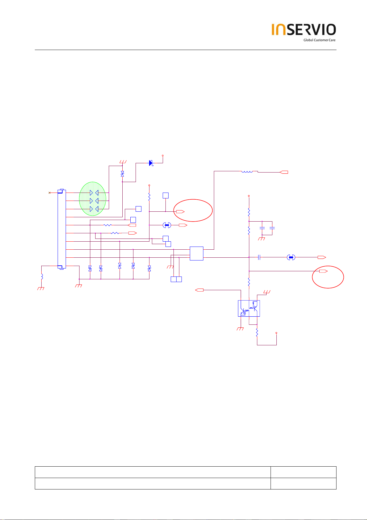
7.4.9 Charging circuit
$$$14
RPWON3
R1=47K
R2=47K
Over-charge voltage
protection circuit
DZ250
UDZS6.2B
3
U253
R2
2
BGND
BGND
BGND
DTC143Z ET1
R1
1
3
R2
2
BQ250
BC807-40W
1
R258
24K
C255
0.1uF16V
R1=4.7K
R2=47K
VBAT
U25 0
R1
DTC
R1=47K
R2=47K
1
N5331054
FUSE(1A 0603)
2
12
3
BGND
R252
5.1K(0603)
U252
1
Vout
2
Vin
XC61CC4402NR
BGND
52
D2 S1 D1
S2G2
3 4
BGND
4
Vss
3
NC
G1
1 6
R251
1K
PCHG3
U251
FDC 6506P
C254
0.1uF16V
BGND
BGND
Fixture
TP26 0
TP250
1
1
PWR
F250
J250
12
BGND
C257
DNI
C258
0.1uF
C250
0.1uF16V
VCHG
from
IOTA's BCI
R257
91
R260
12
BGND
12
12
91
( to IOTA for BB power)
T251
..
TVS
VCCS3
T250
..
TVS
D250
1 2
CRS03
GND
V+
GND
GND
Power Jack
VBATBB
ICTL 3
Pre-charge circuit
Over-voltage protection circuit
If the protection IC within the
battery fails, this circuit can avoid
damaging the battery
1
2
3
4
R256
0.2(1%) 0805
1 2
SJ250 short jump
L250
bead
1uF
C259
VRIO
BGND
VBAT
68K (1%)
R253
BGND
BATEMP3
TP25 1
1
TR2 50
TR_10K
(0402)
HS_TMP 3
TP252
1
C251
22pF
BGND
TP253
1
1
2
3
JP250
VBAT
BATTEMP
GND
BATTERY CONNECTOR
The charging circuit of A38 is composed of charger over-voltage protection circuit and main charging
circuit that are controlled by IOTA. A38’s charging device is the standard 5.4V/0.7A charger
The group of BQ250, R258, DZ250 C255and R252 compose the charger over-voltage protection
circuit. The cut-off voltage is 6.8V. While the charger voltage is over 6.8V, the circuit will turn off
U251 by latching U251.G2 to stop charging. F250 is a 1A fuse to assure charging current under
limit.
The normal charging operation theory is that IOTA monitors charger voltage via VCHG pin to decide
whether charger plug in or out, and control power P-MOSFET (U251) via ICTL pin. If the handset
enters charging mode, Calypso- will follow the charging algorithm to control charging circuit and
monitor charging current by detecting the terminal voltage drop of R256 (0.2 ohm). IOTA controlled
procedure is classified into two parts according to whether battery voltage is higher than 3.2V. IOTA
will execute pre-charge with 40mA to charge the battery via PCHG pin if the battery voltage is lower
than 3.2V. On the other hand, the system will precede normal charging task following by the
charging algorithm.
Technical Documentation Release 1.0
TD_Repair_L3 _Theory of Operation_S38_R1.0.pdf Page 48 of 59
Created by inservio GmbH for BenQ mobile GmbH & Co. OHG - Company Confidential2006©inservio
Page 49

See Appendix A: ‘Charging Algorithm’
VCSS
VBAT
VCHG
VBATS
BCI
MADC
ICTL
ISET2/IO
Technical Documentation Release 1.0
TD_Repair_L3 _Theory of Operation_S38_R1.0.pdf Page 49 of 59
Created by inservio GmbH for BenQ mobile GmbH & Co. OHG - Company Confidential2006©inservio
Page 50

Appendix A: Charging Algorithm
Technical Documentation Release 1.0
TD_Repair_L3 _Theory of Operation_S38_R1.0.pdf Page 50 of 59
Created by inservio GmbH for BenQ mobile GmbH & Co. OHG - Company Confidential2006©inservio
Page 51

Technical Documentation Release 1.0
TD_Repair_L3 _Theory of Operation_S38_R1.0.pdf Page 51 of 59
Created by inservio GmbH for BenQ mobile GmbH & Co. OHG - Company Confidential2006©inservio
Page 52

Technical Documentation Release 1.0
TD_Repair_L3 _Theory of Operation_S38_R1.0.pdf Page 52 of 59
Created by inservio GmbH for BenQ mobile GmbH & Co. OHG - Company Confidential2006©inservio
Page 53

Technical Documentation Release 1.0
TD_Repair_L3 _Theory of Operation_S38_R1.0.pdf Page 53 of 59
Created by inservio GmbH for BenQ mobile GmbH & Co. OHG - Company Confidential2006©inservio
Page 54

Technical Documentation Release 1.0
TD_Repair_L3 _Theory of Operation_S38_R1.0.pdf Page 54 of 59
Created by inservio GmbH for BenQ mobile GmbH & Co. OHG - Company Confidential2006©inservio
Page 55

Technical Documentation Release 1.0
TD_Repair_L3 _Theory of Operation_S38_R1.0.pdf Page 55 of 59
Created by inservio GmbH for BenQ mobile GmbH & Co. OHG - Company Confidential2006©inservio
Page 56

Technical Documentation Release 1.0
TD_Repair_L3 _Theory of Operation_S38_R1.0.pdf Page 56 of 59
Created by inservio GmbH for BenQ mobile GmbH & Co. OHG - Company Confidential2006©inservio
Page 57

Technical Documentation Release 1.0
TD_Repair_L3 _Theory of Operation_S38_R1.0.pdf Page 57 of 59
Created by inservio GmbH for BenQ mobile GmbH & Co. OHG - Company Confidential2006©inservio
Page 58

Technical Documentation Release 1.0
TD_Repair_L3 _Theory of Operation_S38_R1.0.pdf Page 58 of 59
Created by inservio GmbH for BenQ mobile GmbH & Co. OHG - Company Confidential2006©inservio
Page 59

Technical Documentation Release 1.0
TD_Repair_L3 _Theory of Operation_S38_R1.0.pdf Page 59 of 59
Created by inservio GmbH for BenQ mobile GmbH & Co. OHG - Company Confidential2006©inservio
 Loading...