

Page 1
XG-NV2SB
SERVICE MANUAL
S79M2XG-NV2SB
PAL/SECAM/NTSC SYSTEM
LCD PROJECTOR
MODEL
In the interests of user-safety (Required by safety regulations in some countries) the set should be restored
to its original condition and only parts identical to those specified should be used.
XG-NV2SB
CONTENTS
Page Page
• SPECIFICATIONS.............................................. 2
• IMPORTANT SERVICE SAFETY NOTES..........3
• NOTE TO SERVICE PERSONNEL....................4
• OPERATION MANUAL ...................................... 8
• REMOVING OF MAJOR PARTS......................13
• RESETTING THE TOT AL LAMP TIMER..........18
• THE OPTICAL UNIT OUTLINE........................ 19
• CONVERGENCE AND
FOCUS ADJUSTMENT...................................20
• ELECTRICAL ADJUSTMENT .......................... 25
• ADJUSTING THE PC BOARD ......................... 30
• TROUBLE SHOOTING TABLE ........................ 31
• CHASSIS LAYOUT .......................................... 48
• BLOCK DIAGRAM ...........................................50
• OVERALL WIRING DIAGRAM.........................52
• DESCRIPTION OF SCHEMATIC DIAGRAM ...54
• WAVEFORMS .................................................. 55
• SCHEMATIC DIAGRAM................................... 56
• PRINTED WIRING BOARD ASSEMBLIES....100
• PARTS LIST
Ë
ELECTRICAL PARTS............................... 114
Ë
CABINET AND MECHANICAL PARTS.....140
Ë
ACCESSORIES PARTS ........................... 146
Ë
PACKING PARTS ..................................... 146
• PACKING OF THE SET .................................147
SHARP CORPORATION
This document has been published to be used for
after sales service only.
The contents are subject to change without notice.
1
Page 2
XG-NV2SB
Specifications
2
Page 3
XG-NV2SB
2
2
2
IMPORTANT SERVICE SAFETY NOTES
Ë Service work should be performed only by qualified service technicians who are thoroughly
familiar with all safety checks and servicing guidelines as follows:
WARNING
1. For continued safety, no modification of any circuit
should be attempted.
2. Disconnect AC power before servicing.
BEFORE RETURNING THE PROJECTOR:
(Fire & Shock Hazard)
Before returning the projector to the user, perform
the following safety checks:
1. Inspect lead wires are not pinched between the
chassis and other metal parts of the projector.
2. Inspect all protective devices such as non-metallic
control knobs, insulating materials, cabinet backs,
adjustment and compartment covers or shields,
isolation resistor-capacity networks, mechanical
insulators, etc.
3. To be sure that no shock hazard exists, check for
current leakage in the following manner:
» Plug the AC cord directly into a 120-volt AC outlet,
(Do not use an isolation transformer for this test).
» Using two clip leads, connect a 1.5k ohm, 10 watt
resistor paralleled by a 0.15µF capacitor in parallel
between all exposed metal cabinet parts and earth
ground.
» Use an AC voltmeter with sensitivity of 5000 ohm per
volt., or higher, sensitivity to measure the AC voltage
drop across the resistor (See Diagram).
» All checks must be repeated with the AC plug
connection reversed. (If necessary, a non-polarized
adapter plug must be used only for the purpose of
completing these checks.)
Any reading of 0.3 volts RMS (this corresponds to
0.2 milliamp. AC.) or more is excessive and indicates
a potential shock hazard which must be corrected
before returning the unit to the owner.
AC
VOLTMETER
1.5k ohm (10W)
0.15µF
TEST PROBE
TO EXPOSED
METAL PARTS
CONNECT TO KNOWN
EARTH GROUND
234567890123456789012345678901212345678901234567890123456789012123456789012345678901234567890121
234567890123456789012345678901212345678901234567890123456789012123456789012345678901234567890121
SAFETY NOTICE
Many electrical and mechanical parts in LCD Projector
have special safety-related characteristics.
These characteristics are often not evident from visual
inspection, nor can protection afforded by them be
necessarily increased by using replacement components
rated for higher voltage, wattage, etc.
Replacement parts which have these special safety
characteristics are identified in this manual; electrical
components having such features are identified by “å”
and shaded areas in the Replacement Parts Lists and
Schematic Diagrams. For continued protection,
replacement parts must be identical to those used in the
original circuit. The use of a substitute replacement parts
which do not have the same safety characteristics as
the factory recommended replacement parts shown in
this service manual, may create shock, fire or other
hazards.
AVIS POUR LA SECURITE
De nombreuses pièces, électriques et mécaniques, dans
les projecteur à LCD présentent des caractéristiques
spéciales relatives à la sécurité, qui ne sont souvent
pas évidentes à vue.
Le degré de protection ne peut pas être nécessairement
augmentée en utilisant des pièces de remplacement
étalonnées pour haute tension, puissance, etc.
Les pièces de remplacement qui présentent ces
caractéristiques sont identifiées dans ce manuel;
les pièces électriques qui présentent ces particularités
sont identifiées par la marque “å” et hachurées dans la
liste des pièces de remplacement et les diagrammes
schématiques. Pour assurer la protection, ces pièces
doivent être identiques à celles utilisées dans le circuit
d’origine. L’utilisation de pièces qui n’ont pas les mêmes
caractéristiques que les pièces recommandées par
l’usine, indiquées dans ce manuel, peut provoquer des
électrocutions, incendies ou autres accidents.
234567890123456789012345678901212345678901234567890123456789012123456789012345678901234567890121
3
Page 4
XG-NV2SB
NOTE TO SERVICE
PERSONNEL
UV-RADIATION PRECAUTION
The light source, metal halide lamp, in the LCD
projector emits small amounts of UV-Radiation.
A VOID DIRECT EYE AND SKIN EXPOSURE.
To ensure safety please adhere to the following:
1. Be sure to wear sun-glasses when servicing the
projector with the lamp
turned “on” and the top
enclosure removed.
2. Do not operate the lamp outside of the lamp housing.
NOTE POUR LE PERSONNEL
D’ENTRETIEN
PRECAUTION POUR LES RADIATIONS UV
La source de lumière, la lampe métal halide, dans le
projecteur LCD émet de petites quantités de
radiation UV.
EVITEZ TOUTE EXPOSITION DIRECTE
DES YEUX ET DE LA PEAU.
Pour votre sécurité, nous vous prions de respecter
les points suivants:
1. Toujours porter des lunettes de soleil lors d’un
entretien du projecteur
avec la lampe allumée
et le haut du coffret retiré.
2. Ne pas faire fonctionner la lampe à l’extérieur du
boîtier de lampe.
3. Do not operate for more than 2 hours with the
enclosure removed.
UV-Radiation and Medium Pressure
Lamp Precautions
1. Be sure to disconnect the AC plug when replacing
the lamp.
2. Allow one hour for the unit to cool down before
servicing.
3. Replace only with same type lamp. Type
CLMPF0056CE01 or BQC-XGNV6XU/1 rated 100V/
150W.
4. The lamp emits small amounts of UV-Radiation, avoid
direct-eye contact.
5. The medium pressure lamp involves a risk of
explosion. Be sure to follow installation instructions
described below and handle the lamp with care.
3. Ne pas faire fonctionner plus de 2 heures avec le
coffret retiré.
Précautions pour les radiations UV
et la lampe moyenne pression
1. Toujours débrancher la fiche AC lors du
remplacement de la lampe.
2. Laisser l’unité refroidir pendant une heure avant de
procéder à l’entretien.
3. Ne remplacer qu’avec une lampe du même type.
Type CLMPF0056CE01 or BQC-XGNV6XU/1,
caractéristique 100V/150W.
4. La lampe émet de petites quantités de radiation UVéviter tout contact direct avec les yeux.
5. La lampe moyenne pression implique un risque
d’explosion. Toujours suivre les instructions
d’installation décrites ci-dessous et manipuler la
lampe avec soin.
4
Page 5
XG-NV2SB
4
5
UV-RADIATION PRECAUTION (Continued)
23456789012345678901234567890121234567890123
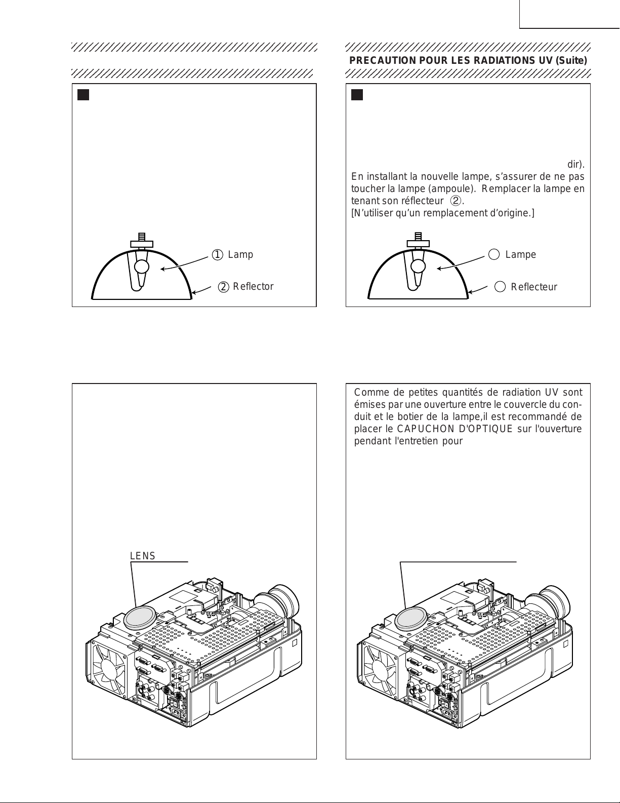
Lamp Replacement
Note:
Since the lamp reaches a very high temperature
during units operation replacement of the lamp
should be done at least one hour after the power
has been turned off. (to allow the lamp to cool off.)
Installing the new lamp, make sure not to touch the
lamp (bulb) replace the lamp by holding its reflector
2.
[Use original replacement only.]
Lamp
1
Reflector
2
DANGER ! –– Never turn the power on without the
lamp to avoid electric-shock or damage of the
devices since the stabilizer generates high voltages
at its start.
PRECAUTION POUR LES RADIATIONS UV (Suite)
234567890123456789012345678901212345678901234
Remplacement de la lampe
Remarque:
Comme la lampe devient très chaude pendant le
fonctionnement de l’unité, son remplacement ne doit
être effectué au moins une heure après avoir coupé
l’alimentation (pour permettre à la lampe de refroidir).
En installant la nouvelle lampe, s’assurer de ne pas
toucher la lampe (ampoule). Remplacer la lampe en
tenant son réflecteur 2.
[N’utiliser qu’un remplacement d’origine.]
1
Lampe
2
Reflecteur
DANGER ! –– Ne jamais mettre sous tension sans
la lampe pour éviter un choc électrique ou des
dommages des appareils car le stabilisateur génère
de hautes tensions à sa mise en route.
Since small amounts of UV-Radiation are emitted
from an opening between the duct cover and the
lamp housing, it is recommended to place the LENS
CAP on the opening during servicing to avoid eye
and skin exposure (Fig. 1).
Note: Please obtain a lens cap before servicing a
model XG-NV2SB that is received without
one.
LENS CAP CAPUCHON D'OPTIQUE
Comme de petites quantités de radiation UV sont
émises par une ouverture entre le couvercle du conduit et le botier de la lampe,il est recommandé de
placer le CAPUCHON D'OPTIQUE sur l'ouverture
pendant l'entretien pour éviter une exposition des
yeux et la peau (Fig. 1).
Remarque: Priére de se procurer un capuchon
d'optique acant d'entretien un modéle
XG-NV2SB qui est livré sans.
Figure 1.
Figure 1.
5
Page 6
XG-NV2SB
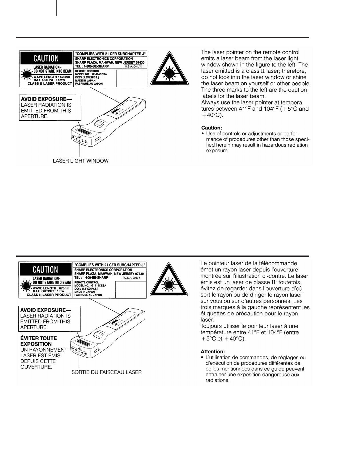
Cautions Concerning the Laser Pointer
Précautions touchant le pointeur laser
6
Page 7
XG-NV2SB
WARNING: High brightness light source, do not stare into the beam of light, or view directly . Be especially
careful that children do not stare directly in to the beam of light.
WARNING: TO REDUCE THE RISK OF FIRE OR ELECTRIC SHOCK, DO NOT EXPOSE THIS UNIT TO
MOISTURE OR WET LOCATIONS.
CAUTION
RISK OF ELECTRIC SHOCK.
DO NOT REMOVE SCREWS
EXCEPT SPECIFIED USER
SERVICE SCREW
CAUTION: TO REDUCE THE RISK OF ELECTRIC SHOCK,
DO NOT REMOVE CABINET.
NO USER-SERVICEABLE P ARTS EXCEPT LAMP UNIT.
REFER SERVICING TO QUALIFIED SERVICE
PERSONNEL.
The lighting flash with arrowhead within a
triangle is intended to tell the user that
parts inside the product are risk of electric
shock to persons.
The exclamation point within a triangle is
intended to tell the user that important
operating and servicing instructions are in
the manual with the projector.
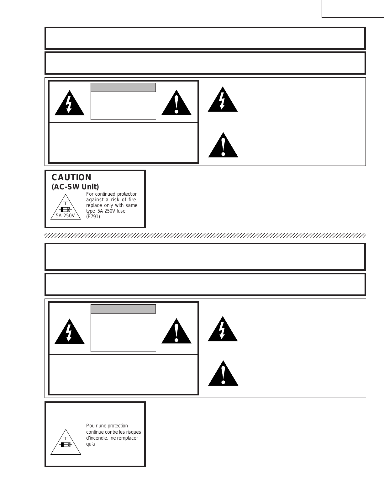
CAUTION
(AC-SW Unit)
5A 250V
A VERTISSEMENT : Source lumineuse de grande intensité. Ne pas fixer le faisceau lumineux ou le regarder
For continued protection
against a risk of fire,
replace only with same
type 5A 250V fuse.
(F791)
directement. Veiller particulièrement à éviter que les enfants ne fixent directement le
faisceau lumineux.
A VERTISSEMENT : AFIN D’EVITER TOUT RISQUE D’INCENDIE OU D’ELECTROCUTION, NE P AS PLACER
CET APPAREIL DANS UN ENDROIT HUMIDE OU MOUILLE.
ATTENTION
RISQUE
D’ELECTROCUTION NE
PASRETIRER LES VIS, A
L’EXCEPTION DES VIS DE
REPARATION UTILISATEUR
SPECIFIEES
ATTENTION: POUR EVITER T OUT RISQUE
D’ELECTROCUTION, NE PAS RETIRER LE CAPOT.
AUCUNE DES PIECES INTERIEURES N’EST REP ARABLE
PAR L’UTILISATEUR, A L’EXCEPTION DE L’UNITE DE
LAMPE. POUR TOUTE REPARA TION, S’ADRESSER A UN
TECHNICIEN D’ENTRETIEN QUALIFIE.
L’éclair terminé d’une flèche à l’intérieur
d’un triangle indique à l’utilisateur que les
pi‘eces se trouvant dans l’appareil sont
susceptibles de provoquer une décharge
électrique.
Le point d’exclamation à l’intérieur d’un
triangle indique à l’utilisateur que les
instructions de fonctionnement et
d’entretien sont détaillées dans les
documents fournis avec le projecteur.
PRECAUTION
(Unite d’interrupteur d’alimentation c.a.)
Pou r une protection
continue contre les risques
d’incendie, ne remplacer
qu’avec un fusible 5A
5A 250V
250V du même type.
(F791)
7
Page 8
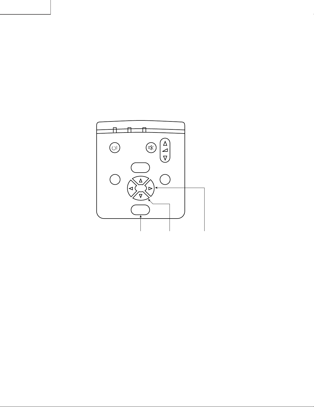
XG-NV2SB
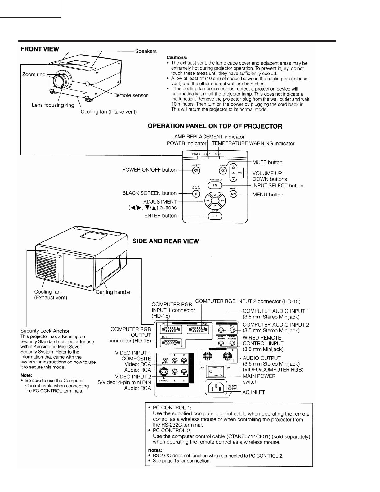
Location of Controls
8
Page 9
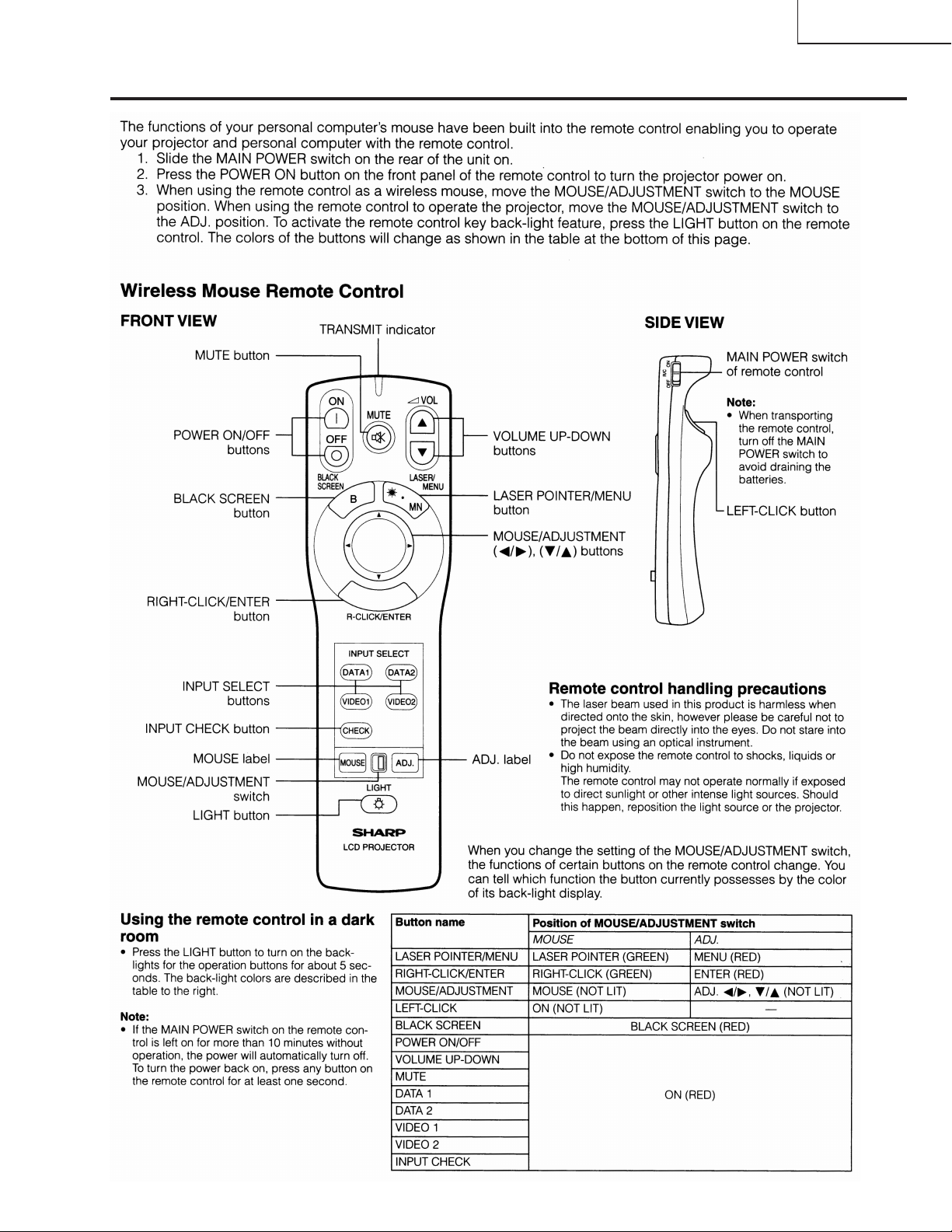
Operating the Wireless Mouse Remote Control
XG-NV2SB
9
Page 10
XG-NV2SB
10
Page 11
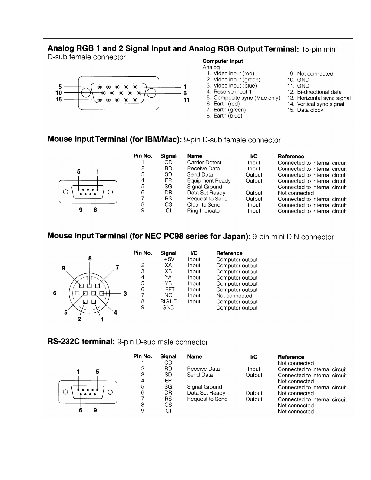
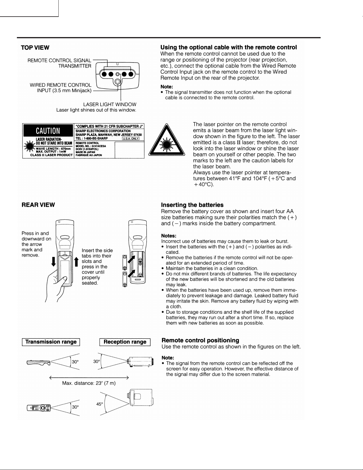
Connection Pin Assignments
XG-NV2SB
11
Page 12
XG-NV2SB
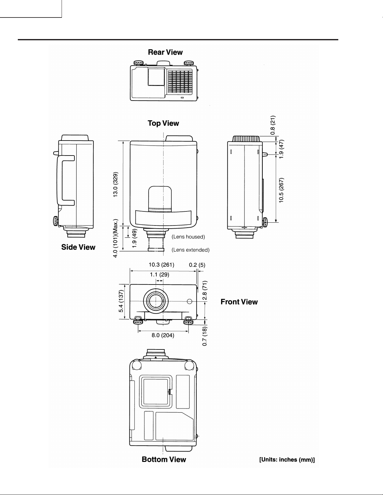
Dimensions
12
Page 13
XG-NV2SB
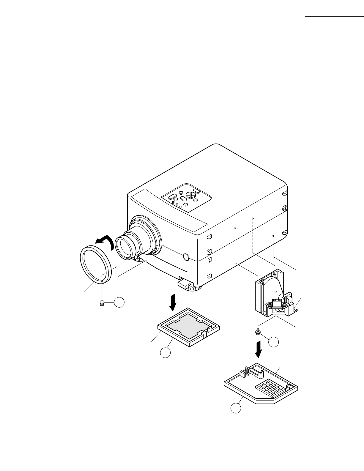
REMOVING OF MAJOR PARTS
1.Removing the Intake cover, lamp unit and lens cover
1-1. Detach the Intake cover.
1-2. Remove the screw off the lamp cage cover and detach the lamp cage cover.
1-3. Remove the three lock screws off the lamp cage unit and detach the lamp cage unit.
1-4. Remove the lock screw from the lens cover. Turn the lens cover clockwise or counterclockwise and detach it.
Notes:
» Before the replacement, turn of f the projector’s power button, make sure the cooling fan comes to a complete
stop, and unplug the power cord.
» The lamp may be still very hot. Turn off the power button, unplug the power cord and wait for at least 1 hour
before staring the job.
» In fitting the lamp cage unit back into position, make sure the connector is at the top position.
Lens Cover
1-4
Intake Cover
Lamp Cage Unit
1-3
1-1
Lamp Cage Cover
1-2
13
Page 14
XG-NV2SB
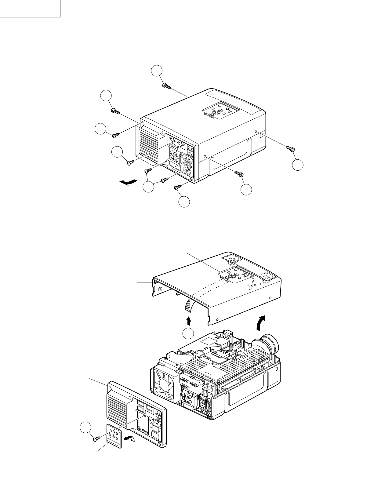
2.Removing the top and rear cabinets
2-1. Remove the five lock screws off the rear cabinet.
2-2. Remove the ten lock screws from the rear cabinet and the terminal plate. Detach the rear cabinet from the
bottom first (because it is hooked at the top).
2-3. Remove the four lock screws off the top cabinet.
2-3
2-3
2-1
2-2
2-3
2-2
2-1
2-3
2-4. While pressing the top center at both sides of the bottom cabinet, pull the ends of the top cabinet outward to
unhook it. Slowly lift the back of the top cabinet, disconnect the operation key PWB connector (KY) and the
speaker connector (SP), and take up and away the top cabinet.
2-5. Remove the lock screw off the video terminal cover and detach the video terminal cover.
Operation Key Unit
Top Cabinet
(SP)
(KY)
2-4
Rear Cabinet
2-5
Video Terminal Cover
14
Page 15
XG-NV2SB
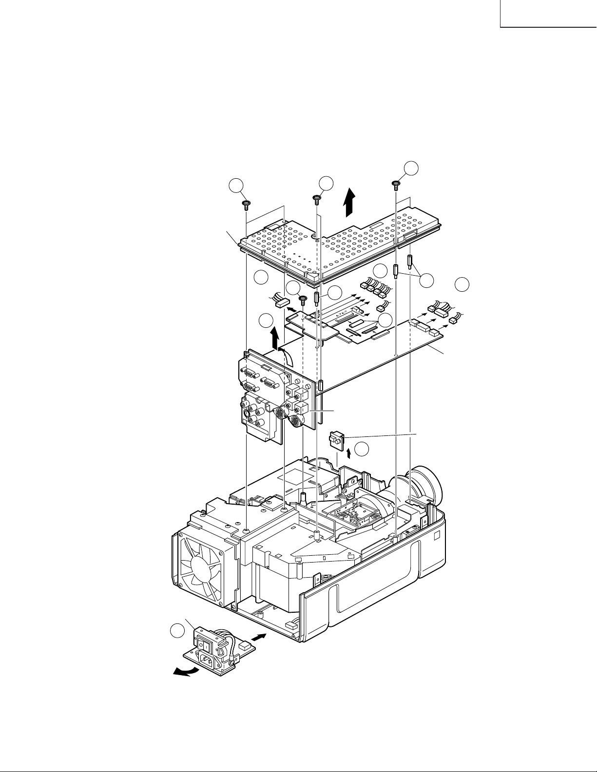
3.Removing the PWBs
3-1. Remove the six lock screws from the PC I/F PWB. Disconnect the output PWB unit connectors. Pull up the PC
I/F PWB off the output PWB unit.
3-2. Remove the three spacers and the lock screw from the output PWB unit. Disconnect the LCD flat cables. Pull
up and away the output PWB unit together with the signal PWB unit on it.
3-3. Flip up the output PWB unit by 90°. Pull it up off the signal PWB unit.
3-4. Hold up the front of the AC switch PWB and draw the PWB out of position.
3-5. Finally detach the remote control receiver PWB.
3-1
3-1
PC I/F Unit
3-1
3-1
3-3
(EA)
3-2
(FN)
3-2
Signal Unit
(FS)
3-5
3-1
(Q)
(PC)
(L)
3-2
3-2
Infrared R/C Receiver Unit
(FE)
(SO)
Output Unit
3-1
(F)
AC-SW Unit
3-4
(PF)CN791
15
Page 16
XG-NV2SB
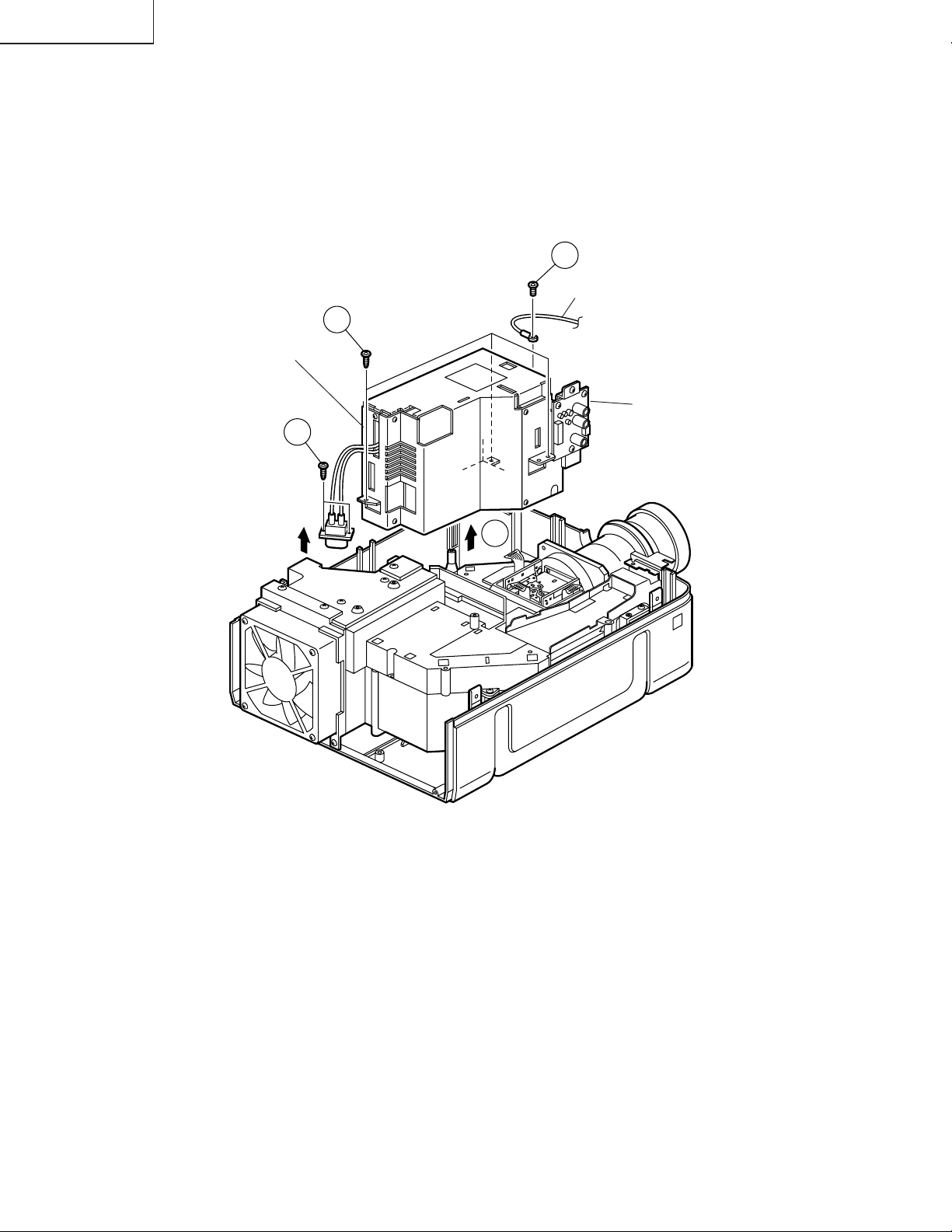
4.Removing the power/ballast PWB assembly
4-1. Remove the three lock screws off the power/ballast PWB assembly.
4-2. Remove the two lock screws off the lamp socket holder and detach the holder.
4-3. Disconnect the ground wire from the filter PWB.
4-4. Lift the power/ballast PWB assembly and take out this assembly.
4-3
4-1
Power/Ballast Unit Ass'y
4-2
to Filter Unit
Sound Out Unit
4-4
16
Page 17
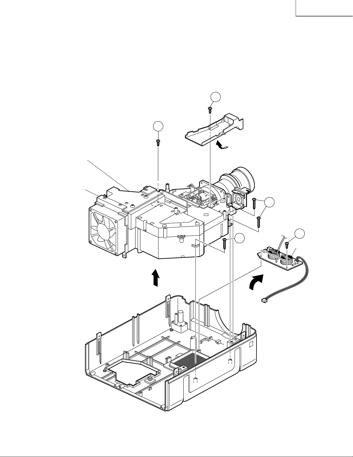
5.Removing the optical mechanism unit
5-1. Remove the lock screw from the IC cooling duct and remove the duct.
5-2. Remove the four lock screws off the optical mechanism unit and detach this unit.
6.Remove the filter PWB
6-1. Remove the two lock screws off the filter PWB and detach this PWB.
5-1
5-2
Optical Mechanism Unit
XG-NV2SB
Duct Fan Unit
5-2
5-2
6-1
Filter Unit
17
Page 18
XG-NV2SB
RESETTING THE TOTAL LAMP TIMER
When the lamp has been replaced, reset the total lamp timer in the following steps.
Resetting procedure
1. While holding down the “ENTER”, “ADJ."” and “ADJ.|” keys on the set at the same time, turn on the main
power switch (located above the AC inlet).
2. Now the total lamp timer is reset to zero. “000H” appears on the screen.
POWER
ON/OFF
BLACK
SCREEN
LAMP TEMP
INPUT SELECT
IN
ENTER
IN
ENTER
MUTE
MENU
MNMN
ADJ."
VOL
ADJ.|
18
Page 19
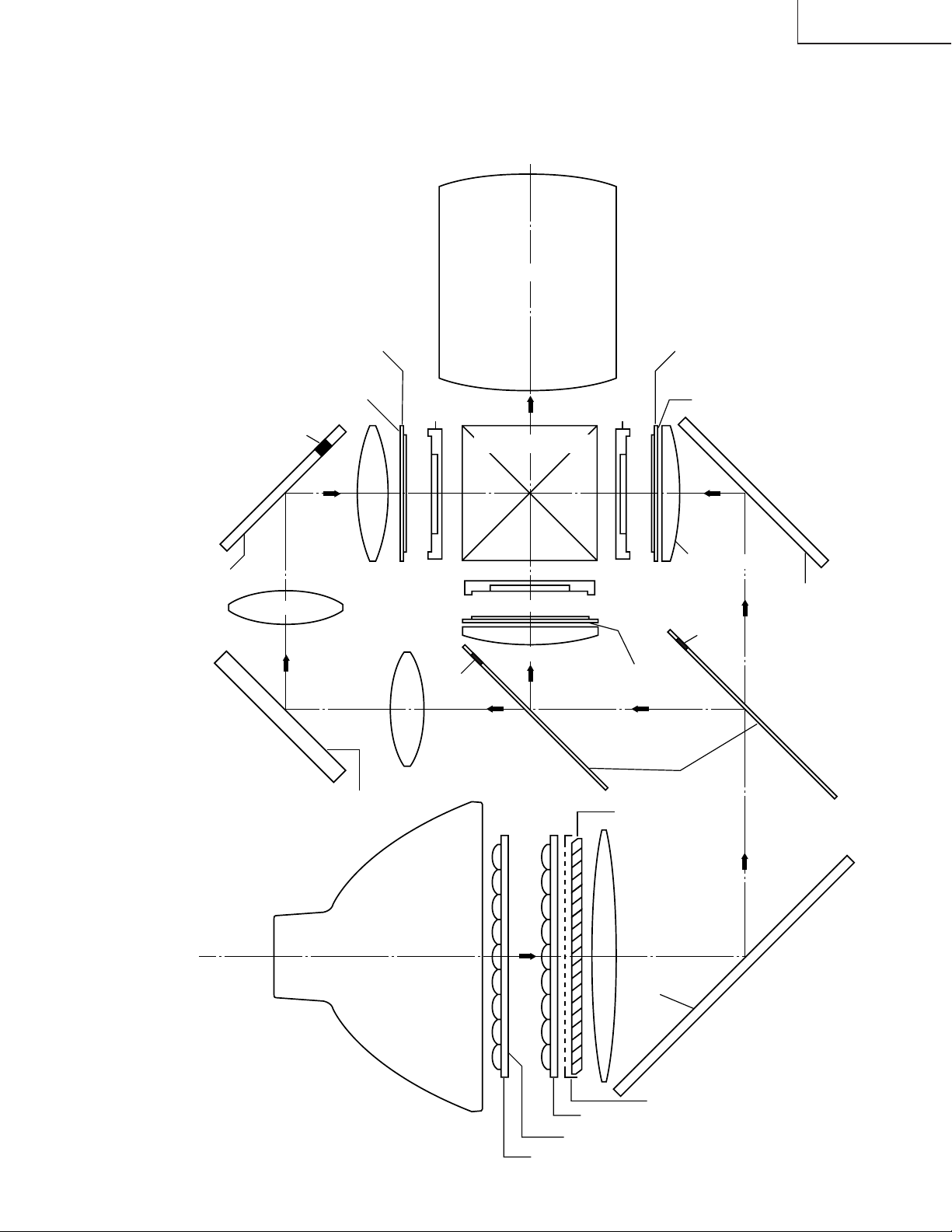
THE OPTICAL UNIT OUTLINE
Layout of the optical system
Note: Layout for positioning the optical system.
XG-NV2SB
Projection Lens
Dichroic coating
(B reflection)
Incident polarizing plate B
Dichroic coating
(B transmission)
Marking
M6
BLUE
B reflector
G03 L2
Relay lens 3
Relay lens 2
G02 L2
AL-coated mirror B
M4
AL-deposited face
B-LCD
Cross dichroic prism
G-LCD
Incident polarizing plate G
Marking
G01
Relay lens 1
Condenser lens G
GREEN
BLUE
G reflector
* M3
R-LCD
Dichroic coating
(G reflection)
Dichroic coating
PBS(polarization
beam splitter)
Incident polarizing plate R
Dichroic coating
(R transmission)
AL-coated mirror R
M5
Condenser lens R
AL-deposited face
RED
Marking
(R reflection)
M2
B/G reflector
* The M3 mirrors have a coating
wedge (for different film thickness). Set up these mirrors, with
their markings positioned as
shown above, so that their
coated faces and both sides be
in the correct directions.
UHP lamp
(Light source)
Fly-eye lens (outgoing light)
UV-IR coating
Fly-eye lens (incoming light)
19
L1
AL-deposited
face
PBS aperture
M1
AL-coated mirror W
Page 20

XG-NV2SB
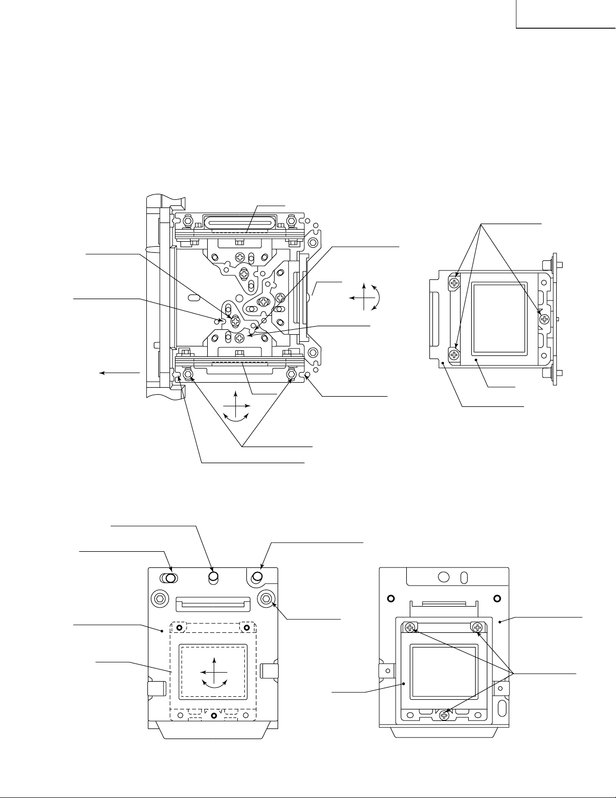
CONVERGENCE AND FOCUS ADJUSTMENT
» Start the convergence and focus adjustments with the top cabinet and the LCD covers
(Top/Bottom) removed but the power on. Use the remote control to adjust the image.
Take the following procedures.
1. Focusing the projection lens
(A) Replacing all the 3 LCD panels
1. Before replacing all the 3 LCD panels, project an image on the screen and bring it into focus.
2. Replace the panels with new ones. But until the focus has been completely readjusted, be careful not to
change the distance between the set and the screen, nor to move the projection lens focus and zoom
rings.
If the focus is readjusted with a different positional relation, the relation between the projection distance
and the screen size is affected. In other words, a short-distance image (40 WIDE, for example) may get
out of the focus range, or a long-distance image (300 WIDE, for example) may come out of focus.
(B) Replacing 1 or 2 of the 3 LCD panels
1. In adjusting the focus after replacement of one or two LCD panels, project an image on the screen and turn
the projection lens focus ring to get the non-replaced LCD panel into focus.
2. But until the focus has been completely adjusted for the new LCD panels, be careful not to change the
distance between the set and the screen, nor to move the projection lens focus and zoom rings.
(If the distance has been changed or the projection lens readjusted, repeat the above steps 1 and 2.)
2. Adjusting the G-LCD panel
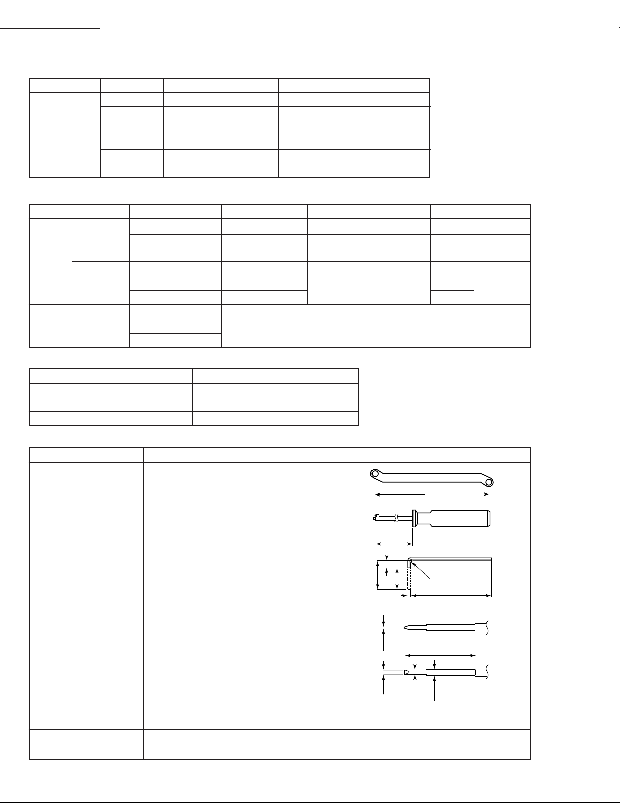
(A) Focus adjustment. (Make this adjustment on the white-only screen.)
1. Right-and-left focus adjustment (θY direction) .
Loosen the lock screws "b" and "c" and insert the eccentric screwdriver into the notch and hole "b". Turn
the screwdriver until the right and left halves on the screen get into focus.
First get the right and left halves in balance. Then improve the accuracy while making the adjustment 2
below.
2. Top-center-bottom focus adjustment (θX and Z directions).
Loosen the lock screws "a" and "c" and insert the eccentric screwdriver into the notch and hole "a" or "c".
Turn the screwdriver until the top, center and bottom on the screen get into focus. In adjusting this top-tobottom focus, temporarily tighten the lock screw "b" to fix the θY direction adjustment.
3. Repeat the above steps 1 and 2 to finely adjust the focus. Finally tighten up all the lock screws.
Notes :
1 Carefully proceed with the focus adjustment because the adjusting directions are correlated.
2 In adjusting the convergence and focus, do not move the projection lens zoom and focus rings until the end
of all the adjustments.
(B) Convergence adjustment
» The G-LCD panel has no convergence adjustment mechanism. Use this panel as convergence adjustment
reference.
3. B-LCD panel adjustment (the same for the R-LCD panel)
(A) Focus adjustment
» T ake the same procedure as for the G-LCD panel focus adjustment. Note that the adjustment range is small
in the Z direction. If the convergence is quite different between the B-LCD and G-LCD panels, roughly adjust
the convergence first and then the focus.
(B) Convergence adjustment
» Use a crosshatch pattern signal for this adjustment.
Make the adjustment just for the G-color and the relevant color.
(1) Loosen the convergence lock screw "d".
(2) With the G-LCD panel’s screen center as reference, adjust the B-LCD panel in the X, Y and θZ directions.
(3) Finally tighten up the convergence lock screw "d".
20
Page 21
Notes :
1 The eccentric cam is used for convergence adjustment. This means that the cam’s turning and the linear
movement are not always uniform.
2 This model is not equipped with the LCD image adjustment mechanism. This is because the dichroic prism
is used for image formation. When the LCD panels all get into the best focus, the images are almost
completely converged.
Convergence and Focus Adjustments Mechanism
XG-NV2SB
TOP VIEW
Lock screw "a"
Notch and hole "a"
(Use an eccentric
screwdriver.)
FRONT
R-LCD
B-LCD
Z
X
θY
Lock screws "c"
Notch and hole "c"
(Use an bladed screwdriver.)
Notch and hole "b"
(Use an eccentric
screwdriver.)
G-LCD
Lock screw "b"
(θY direction)
Notch and
hole "c"
(Use on eccentric
screwdriver.)
X
Z
SIDE VIEW
G-LCD panel
mounting screws
θY
G-LCD
G adjusting plate
SIDE VIEW (from inside)
Eccentric cam
(X direction adjustment)
Eccentric cam
(Y direction adjustment)
R•B adjusting plate
R•B-LCD
SIDE VIEW (from outside)
Eccentric cam
(θZ direction adjustment)
Lock screw "d"
(convergence
adjustment)
Y
X
θZ
R•B-LCD
R•B adjusting plate
R•B-LCD panel
mounting screws
21
Page 22
XG-NV2SB
2
5
16
R2
50
CUT
100
Convergence and Focus Adjustments at a Glance
Adjustment directions
Adjustment Direction Definition Direction of LCD panel
X direction LCD right and left
Convergence Y direction LCD top and bottom
θZ direction Rotation around Z axis LCD turning axis
Z direction LCD optical axis
Focus θX direction Rotation around X axis LCD top-to-bottom flapping
θY direction Rotation around Y axis LCD right-to-left flapping
Convergence and Focus Adjustment for the XG-NV2 Optical Mechanism
Color Adjustment Direction
X direction ±0.8mm Eccentric cam Eccentric cam adjusting wrench d Hex wrench
Convergence Y direction ±0.8mm Eccentric cam Eccentric cam adjusting wrench d Hex wrench
R/B θZ direction ±1° Eccentric cam Eccentric cam adjusting wrench d Hex wrench
colors Z direction ±0.8mm
Focus θX direction ±1°
θY direction ±1°
Z direction ±0.2mm
G color Focus θX direction ±1° Same as for R and B colors
θY direction ±1°
Movement
Position Adjusting tool
Notch and hole "a" & "c"
Notch and hole "a" & "c"
Notch and hole "b" & "c"
Eccentric screwdriver, a, c
Bladed screwdriver a, c
Lock screw
b, c
Tightening tool
Phillips
screwdriver,
*Hex wrench
Focus Adjustments the Other Way
Lock screw Position Related direction
a Notch and hole "a" Z and θX directions
b Notch and hole "b" θY direction
c Notch and hole "c" Z, θX and θY directions
Convergence and Focus Adjusting and Tightening Tools
Tool Specific or General Tool code Configuration
Eccentric cam Specific 9DASPN-XGNV1U
adjusting wrench
80
Eccentric screwdriver Specific 9EQDRiVER-NV1A
Hex wrench General (redesigned) 9EQLNC-XGNV1U
0.5
Bladed screwdriver General 9EQDRiVER-NV1B
3.5
ø3.5
min85
ø5
Phillips screwdriver General — For M2.6 pan-head machine screw
*Hex wrench General —
22
Preferably use a 70 mm or longer
screwdriver (with a handle).
Page 23
XG-NV2SB
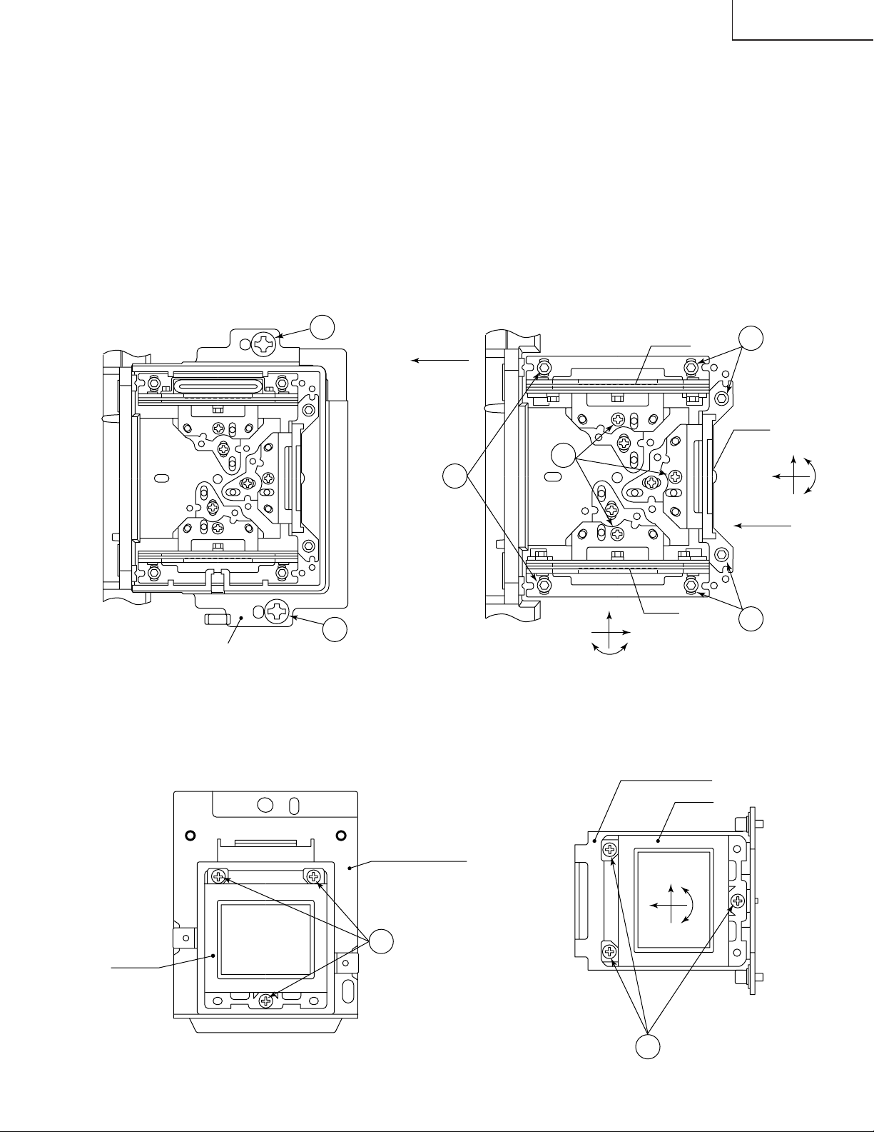
Replacing the LCDs
With the top cabinet removed
(1)Disconnect the LCD flat cable from the output PWB connector.
(2)Remove the two screws of the LCD cover.
(3)Remove the lock screws "b" and "c". Detach the R/B adjusting plate or the G adjusting plate together with the LCD
panel.
(4)Separate the LCD panel from the adjusting plate.
(5)Mount a new LCD panel in the reverse order of the above steps (1), (2), (3) and (4).
~ Readjust the convergence and focus. Note that the G LCD panel needs no convergence adjustment and has
a small adjustment range in the Z direction.
TOP VIEW
LCD cover
TOP VIEW
2
FRONT
Lock
screws "b"
R-LCD
3
3
Lock
screws "c"
Lock screws "c"
3
G-LCD
X
θY
Z
~
X
θY
B-LCD
3
Lock screws "c"
Z
2
SIDE VIEW
R•B-LCD
R•B adjusting plate
4
R•B-LCD panel
mounting screws
23
SIDE VIEW
G adjusting plate
G-LCD
X
θZ
Y
G-LCD panel
4
mounting screws
Page 24
XG-NV2SB
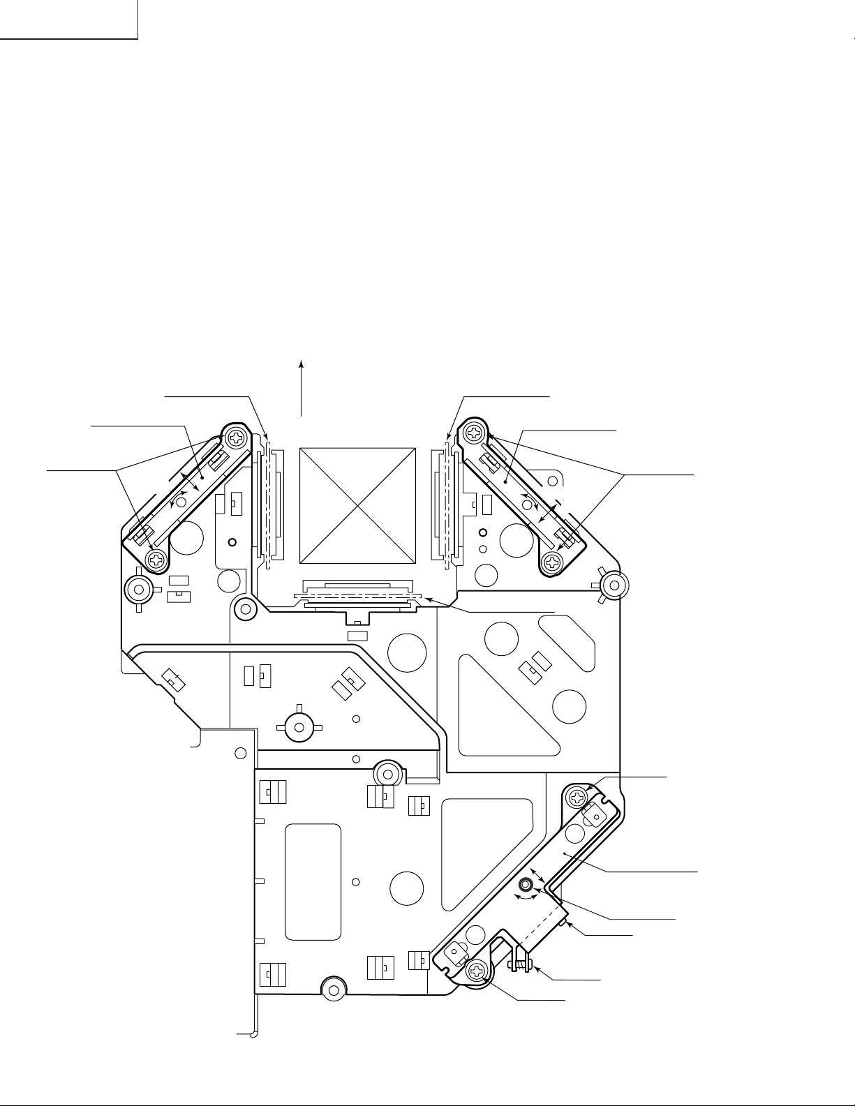
Adjusting the optical axis of the mirrors (M1, M5 and M6)
The optical axis must be readjusted if an eclipse happens with the R. G or B mirrors. Generally speaking,
this adjustment is needed when any of the internal optical components has been replaced.
Adjustment procedure required when any of the panels has been replaced or the convergence has been
adjusted
(1)Disconnect the flat cables of all the LCD panels.
(2)Let the lamp light up.
(3)To adjust the G mirror, shield the R and B mirrors with shielding plates (You can use a business card or the like to
block the light).
(4)Loosen the lock screw of the M1 adjust lever.
(5)Adjust the color discrepancy on the screen by turning the screws A and B.
(6)To adjust the R mirror, shield the G and B mirrors and adjust the M5 adjust lever. For the B mirror, shield the R and
G mirrors and adjust the M6 adjust lever.
(Take the same steps 4 and 5 above.)
(7)Remove all the shielding plates to have a white image.
Make sure there is no eclipse.
M6
Lock screws
Shielding plate B
adjust lever
slide
turn
FRONT
Shielding plate R
M5
Shielding plate G
adjust lever
Lock screws
turn
slide
Screws
24
turn
Screws
slide
ScrewB
M1
Lock screws
ScrewA
adjust lever
Page 25
XG-NV2SB
ELECTRICAL ADJUSTMENT
Hook up a signal generator, or a DOSV or Mac personal computer to the projector in order to feed the
signals specified in the Adjusting conditions.
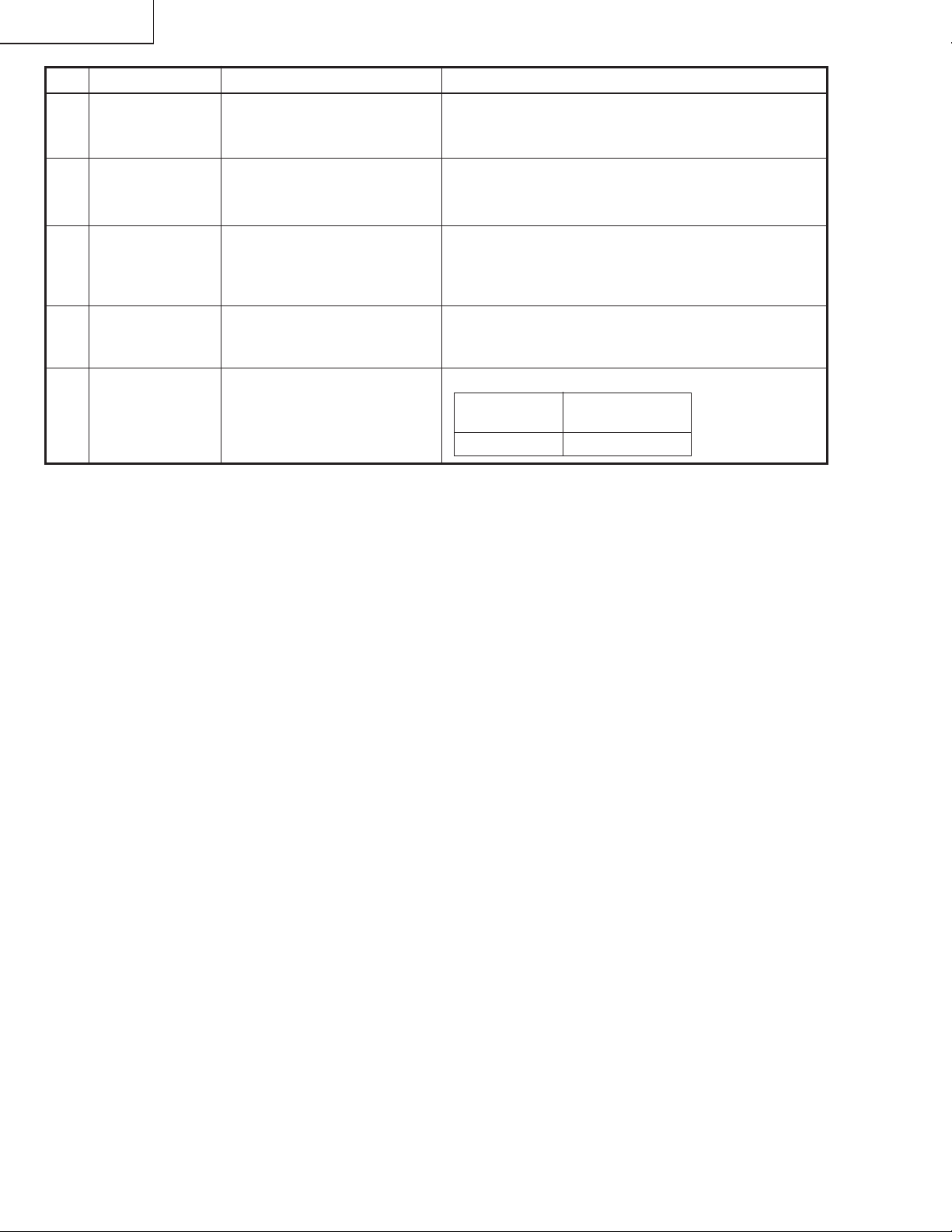
No. Adjusting point Adjusting conditions Adjusting procedure
1 EEPROM
initialization
1. Turn on the power (make
sure the lamp lights up) and
warm up the unit for 15 minutes.
» Make the following settings:
Press S5001 to call up the process mode and
execute S2 in the SSS menu. Now the system, with
the PC board not included, is initialized. Do not
execute S1 because otherwise the PC board will be
initialized.
To adjust the PC board, follow the instruction in
"Adjusting the PC board". (See page 30)
2 R drive 1. Make the following choice.
Group : A/D
Subject : GAIN
Make sure the GAIN value
is 163.
2. Feed the 100% red-only
signal, SVGA (800 x 600)
60Hz, 700mV at PC IN connector.
Group : A/D
Subject : R-D
3 B drive 1. Feed the 100% blue-only
signal, SVGA (800 x 600)
60Hz, 700mV at PC IN connector.
Group : A/D
Subject : B-D
» Using the control switches or the remote controller
buttons, adjust the data so that the signal becomes
bit-less (noise).
» Using the control switches or the remote controller
buttons, adjust the data so that the signal becomes
bit-less (noise).
4 G drive 1. Feed the 100% green-only
signal, SVGA (800 x 600)
60Hz, 700mV at PC IN connector.
Group : A/D
Subject : G-D
25
» Using the control switches or the remote controller
buttons, adjust the data so that the signal becomes
bit-less (noise).
Page 26
XG-NV2SB
No. Adjusting point Adjusting conditions Adjusting procedure
5 RGB 1 system
black level
signal amplitude
(odd-numbered)
1. Make the following choice:
Group : OUTPUT 1
Subject : R1-BLK
R1-GAIN
For green, choose the subjects G1-BLK and G1GAIN.
For blue, choose the subjects B1-BLK and B1-GAIN.
» Choose the subject R1-BLK and adjust the black
peak level to 2.7 ±0.1V DC using the control switches
or the remote controller buttons.
» Next, choose the subject R1-GAIN and adjust the
signal amplitude to 2.9 ±0.1 Vp-p.
» Make the same adjustment for green and blue.
6 RGB 2 system
black level
signal amplitude
(even-numbered)
2. Connect the oscilloscope to
pin (4)(TP1 101) of SC1101
for red.
Pin (4)(TP1201) of
SC1201 for green
Pin (4)(TP1301) of
SC1301 for blue
1. Make the following choice:
Group : OUTPUT 2
Subject : R2-BLK(R),
R2-GAIN
For green, choose the subjects G2-BLK and G2GAIN.
For blue, choose the subjects B2-BLK and B2-GAIN.
2. Connect the oscilloscope to
pin (6)(TP1 102) of SC1101
for red.
Pin (6)(TP1202) of
SC1201 for green
Pin (6)(TP1302) of
SC1301 for blue
2.9Vp-p
2.7V DC
» Choose the subject R2-BLK and adjust the black
peak level to 2.7 ±0.1V DC using the control switches
or the remote controller buttons.
» Next, choose the subject R2-GAIN and adjust the
signal amplitude to 2.9 ±0.1 Vp-p.
2.9Vp-p
2.7V DC
» Make the same adjustment for green and blue.
7 Sample-and-
hold pulse
phase
RCK-PHASE
GCK-PHASE
BCK-PHASE
1. Feed the XGA mode 75-Hz
black signal.
2. Make the following choice:
Group : OUTPUT 3
Subject : SH-PHASE
(Have the standard level at
8.)
Fix the R-, G- and BPHASE settings all to 4.
» Feed the SVGA gradation pattern single-color sig-
nal and make sure that there is no difference in
brightness between adjacent vertical lines. If there
is a difference, make fine adjustment by choosing
the following subjects.
R2-GAIN for red
G2-GAIN for green
B2-GAIN for blue.
» Using the control switches or the remote controller
buttons, make sure that the “OUTPUT 3” characters
are not blurry and there is no ghost image. If such
blur or ghost occurs, finely adjust the setting in the
range of 7~9.
26
Page 27
No. Adjusting point Adjusting conditions Adjusting procedure
8 RGB counter-
voltage
adjustment
1. Feed the black-and-red
(25%) stripe signal (SVGA)
to RGB1.
» Using the control switches or the remote controller
buttons, adjust the data in order to minimize the
flicker.
XG-NV2SB
9 RGB white
balance
10 Horizontal
center
2. Make the following choice:
Group : OUTPUT 3
Subject : RC (R)
3. Change to the outer RG1 at
the shoot of the operating
switches or the remote controller buttons.
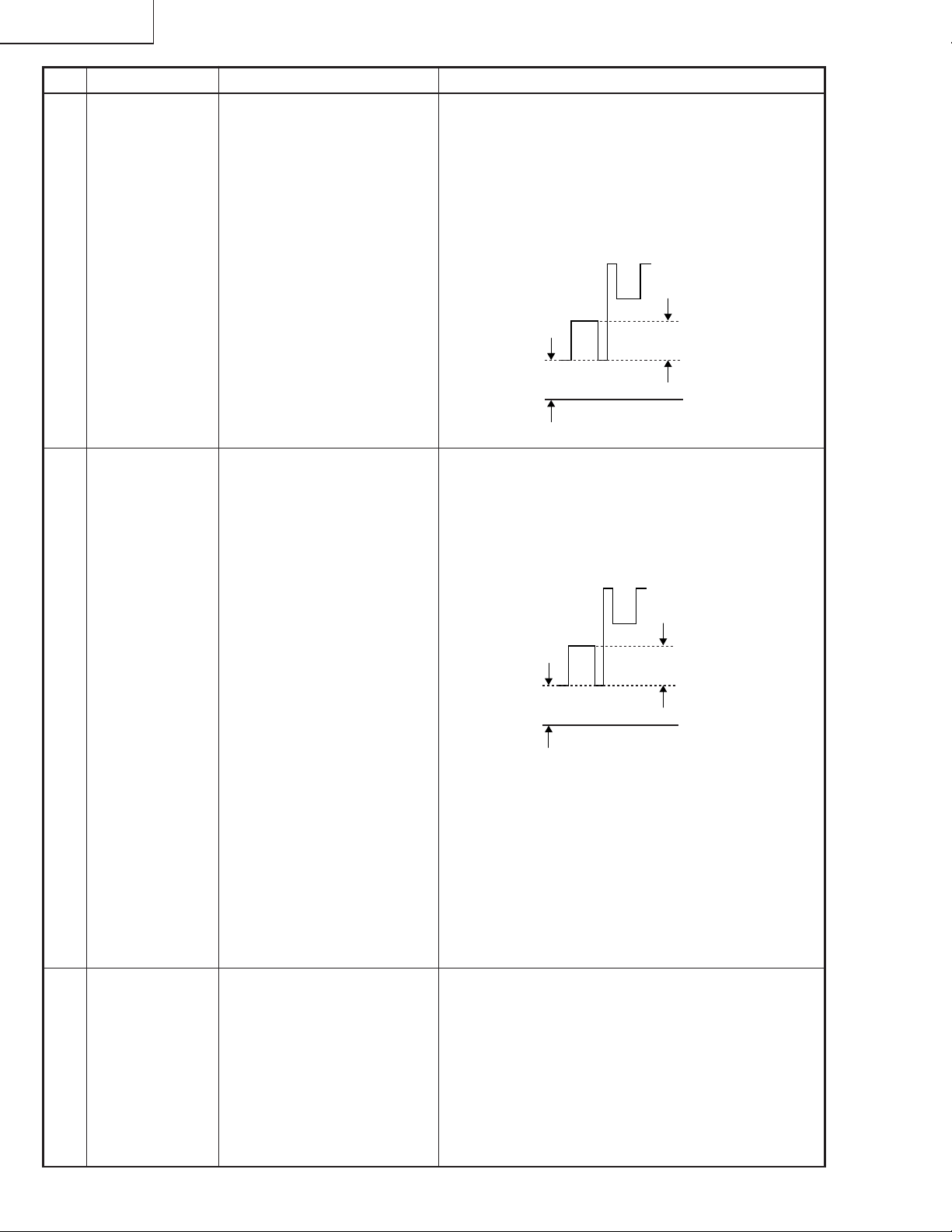
1. Feed the 32-step gray scale
signal (SVGA).
Group : OUTPUT 1
Subject : R1-BLK
R1-GAIN (R)
B1-BLK
B1-GAIN (B)
1. Feed the NTSC monoscope pattern signal.
» Make the same adjustment for BC (B) and GC (G).
» See if the image is equally adjusted at the center
and both sides of the screen. If not, readjust the
setting to have the image equal at right and left.
» Choose the subjects R1-BLK and B1-BLK and
adjust the black balance of the gradation. Choose
the subjects R1-GAIN and B1-GAIN and adjust the
gray-to-while balance.
» Using the control switches or the remote controller
buttons, adjust the data to have the same overscan.
11 Video picture
adjustment
2. Group : VIDEO 2
Subject : N358-DLY
N443-DLY
PAL-DLY
SECAM-DLY
Make sure all the settings
are zero (0).
3. Group : VIDEO 1
Subject : NTSC-H
1. Feed the split color bar signal.
Group : VIDEO 1
Subject : PICTURE
2. Connect the oscilloscope
between pin (2) of P801
and GND.
» Using the control switches or the remote controller
buttons, adjust the black-to-white (100%) level
difference to 2.2 ±0.02 Vp-p.
2.2 Vp-p
27
Page 28
XG-NV2SB
No. Adjusting point Adjusting conditions Adjusting procedure
12 Video AGC 1. Feed the split color bar sig-
nal.
Group : VIDEO 1
Subject : AGC
2. Connect the oscilloscope
between pin (2) of P801
and GND.
13 Video
brightness
adjustment
1. Feed the baseband (split
color bar) signal. (The ONAIR signal is not accepted
because of its too much
noise.)
Group : VIDEO 1
Subject : BRIGHT
2. Press the control switch or
the remote control’s mute
button (to set the gamma
correction to the process
setting).
» Using the control switches or the remote controller
buttons, adjust the black-to-white (100%) level
difference to 1.65 ±0.02 Vp-p.
1.65 Vp-p
» Using the control switches or the remote controller
buttons, adjust the setting until the black signal
becomes bit-less.
14 Tint 1. Feed the split color bar sig-
nal.
Group : VIDEO 1
Subject : TINT
2. Connect the oscilloscope to
pin (5) of P801.
15 NTSC color
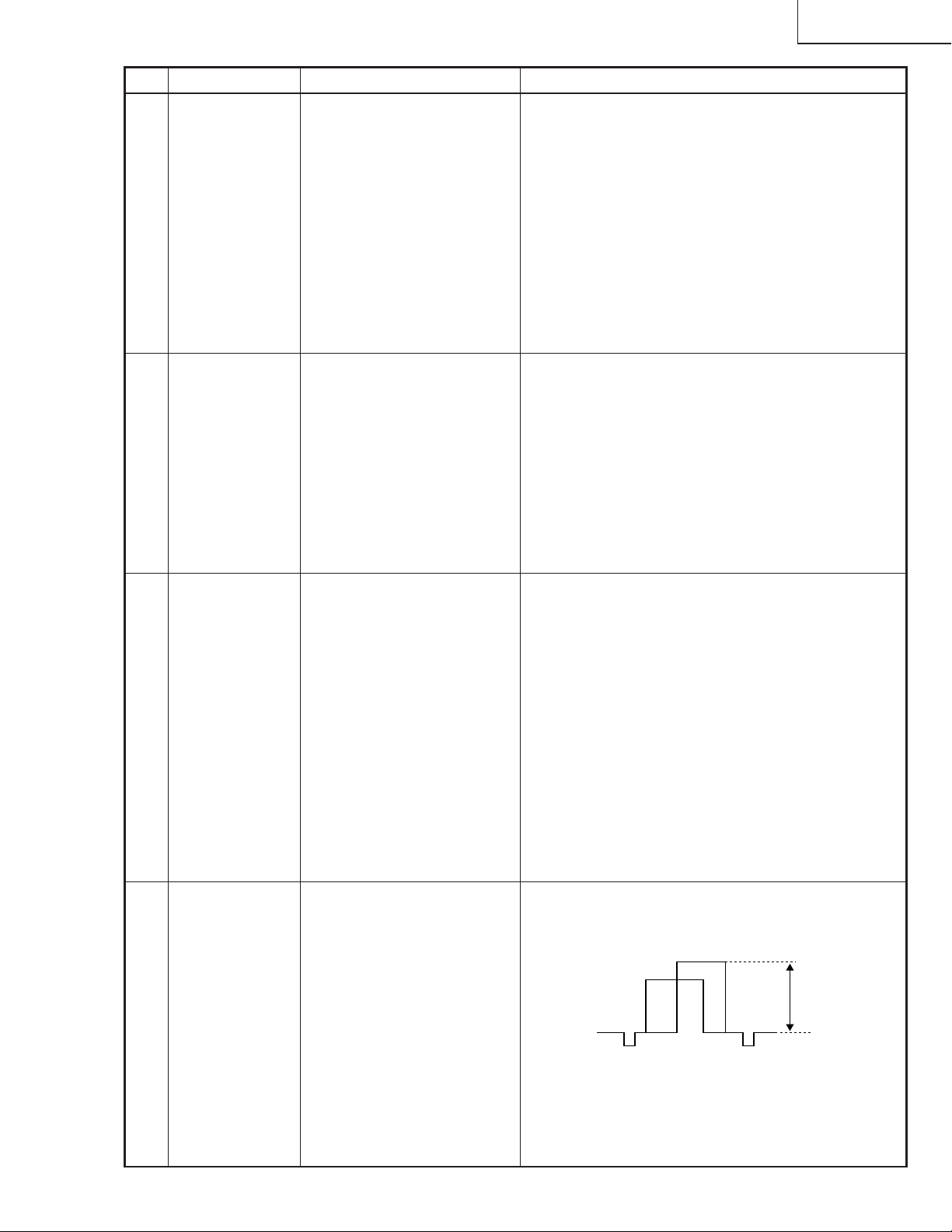
saturation level
1. Feed the split color bar signal.
Group : VIDEO 1
Subject : N-COLOR
2. Connect the oscilloscope to
pin (1) of P801.
» Using the control switches or the remote controller
buttons, adjust the data to have the -(B-Y) waveform downhill straight.
» Using the control switches or the remote controller
buttons, adjust the difference between the 100%
white portion and the red portion to 0.1 ±0.02 Vp-p.
100% White Red
0.1Vp-p
28
Page 29
No. Adjusting point Adjusting conditions Adjusting procedure
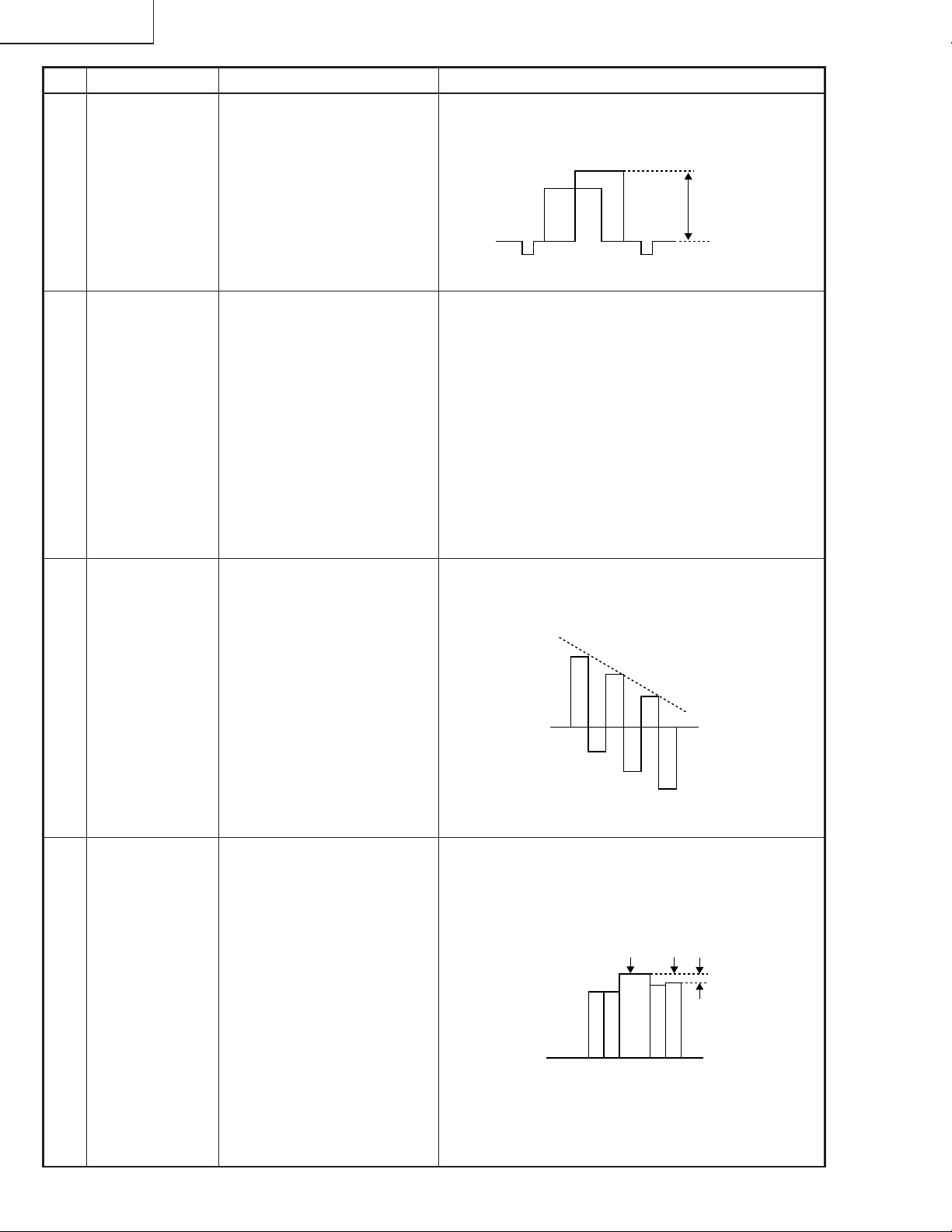
16 PAL color
saturation level
1. Feed the P AL color bar signal.
Group : VIDEO 1
Subject : P-COLOR
2. Connect the oscilloscope to
pin (1) of P801.
» Using the control switches or the remote controller
buttons, adjust the difference between the 100%
white portion and the red portion to 0.48±0.02 Vp-p.
100% White Red
0.48Vp-p
XG-NV2SB
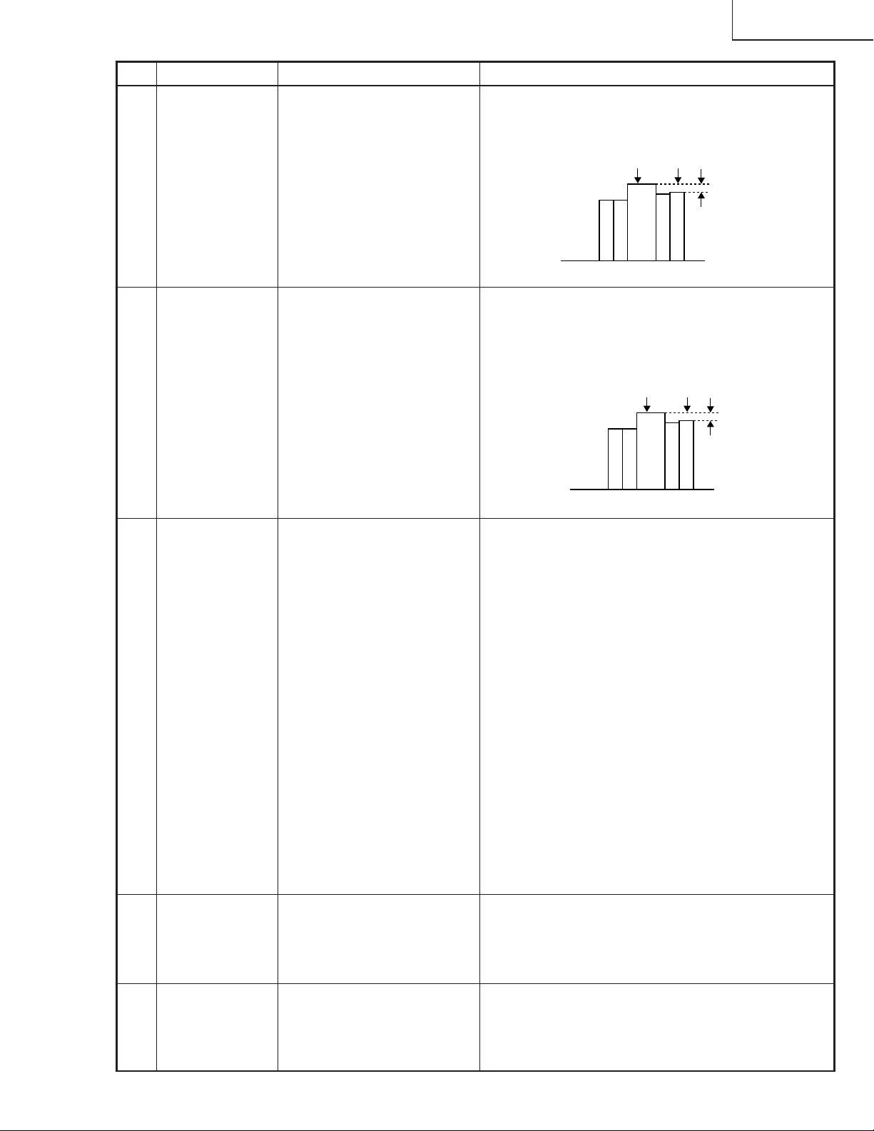
17 SECAM color
saturation level
18 Video white
balance
1. Feed the SECAM color bar
signal.
Group : VIDEO 1
Subject : S-COLOR
2. Connect the oscilloscope to
pin (1) of P801.
1. Feed the NTSC monoscope pattern signal.
Group : VIDEO 2
Subject : R1-GAIN
B1-GAIN
» Using the control switches or the remote controller
buttons, adjust the data to have a level difference of
0.48 ±0.02 Vp-p between the 100% white portion
and the red portion.
100% White Red
0.48Vp-p
» Using the control switches or the remote controller
buttons, adjust the data so that the white balance
be just the best white balance.
If the black side is not properly adjusted, first
readjust the black side by making the following
choice:
Group :OUTPUT 1
Subject:R1-BLK
B1-BLK
Then, make the following choice:
Group :VIDEO 2
Subject:R1-GAIN
B1-GAIN
19 Color system
performance
check
20 Video system
performance
check
1. Receive the color bar signal.
1. Receive the monoscope
pattern signal.
29
Readjust the related data.
Since the subjects R1-BLK and B1-BLK are common for the RGB input and VIDEO input, feed the
RGB signal again to adjust the white balance.
» In the process mode and select L1. Check the color
and tint.
» In the process mode and select L2. Check the pic-
ture, brightness and sharpness.
Page 30
XG-NV2SB
No. Adjusting point Adjusting conditions Adjusting procedure
21 Audio system
performance
check
» In the process mode nad select L3. Check the bass,
treble and balance.
22 RGB
performance
check
23 Off-timer
performance
check
24 Thermistor
performance
check
25 Factory settings
1. Receive the RGB signal.
1. Heat the thermistor using a
dryer.
» In the process mode and select L4. Check the pic-
ture, brightness, red, blue, clock, phase, horizontal
position, and vertical position.
» In the process mode and select OFF . Make sure that
the off-timer starts with “5” (minutes), counts down
each minute in 1 second, and turns off the set at “0”.
» Make sure the “TEMP” is displayed.
» Make the following settings.
Process
adjustment
S4 “Factory setting 4”
Remote controller
setting
Adjusting the PC board (CPCi-0025CE04. PC I/F Unit)
1.Initializing te EEPROM
1) Press the S5001 key to call the process mode.
2) Execute S1 on the SSS menu. (The S1 is used to initialize the PC board alone. Do not execute S2 because
otherwise all the adjusted data but the PC board will be initialized.)
2.Adjusting the level settings
2-1. Oscilloscope range setting
Set the range to DC 1V/div. and 5µs/div.
2-2. Input signal
Feed the SVGA 800x600 60Hz gradation waveform signal.
2-3. Adjusting and checking the level settings
1) Press the S5001 key to call the process mode.
2) Adjust the SH-PHASE setting on the "OUTPUT 3" menu until the "OUTPUT 3" characters are not blurry any
longer.
3) Connect a oscilloscope to TP2. Adjust the BRIGHT setting of "OUTPUT 2" to have the black level of the signal
at 1.7V.
4) Adjust the ROS setting on the A/D menu until the voltage at the positive pole of C64 or pin (2) of IC1 1 becomes
1.7V .
5) Adjust the GOS setting on the A/D menu until the voltage at the positive pole of C57 or pin (2) of IC10 becomes
1.7V .
6) Adjust the BOS setting on the A/D menu until the voltage at the positive pole of C50 or pin (2) of IC9 becomes
1.7V.
7) Make sure the GAIN setting on the A/D menu is 163.
8) Connect the oscilloscope to TP1. Adjust the R-D setting on the A/D menu until the white top level of the signal
becomes 3.6V. (Make sure that both the black and white graduations are visible clearly.)
9) Connect the oscilloscope to TP3. Adjust the B-D setting on the A/D menu until the white top level of the signal
becomes 3.6V. (Make sure that both the black and white graduations are visible clearly.)
10) Connect the oscilloscope to TP2. Adjust the G-D setting on the A/D menu until the white top level of the signal
becomes 3.6V. (Make sure that both the black and white graduations are visible clearly.)
11) Press the S5001 key to exit from the process mode.
30
Page 31

TROUBLE SHOOTING TABLE
Checking the PWB performance
XG-NV2SB
Video input in trouble
Go to "Checking the video unit
circuit".
RGB input in trouble
Feed test pattern signal from
PC.
Is specified cable connected
between PC and projector?
Yes
Is supply voltage as specified?
Yes
Does image appear?
Yes
Go to "Checking the PC I/F
unit ".
Through-output in trouble
Through-output circuit in
trouble.
No
Use specified cable.
No
Power circuit in trouble.
No
Check the connectors, starting
from the PC unit input circuit.
Remote control in trouble
Go to "Checking the remote
control circuit".
31
Page 32

XG-NV2SB
Checking the video system
TROUBLE SHOOTING TABLE (Continued)
Is the lamp on?
Is specified voltage fed to EA
connectors? Also, is the voltage signal
P1501 and P1502 right?
Are there signal inputs at pins (40)
and (45) of IC806?
Are there signal outputs at pins (3)
and (6) of IC816?
Yes
Go to "Checking IC801
(RGB signal output circuit)".
No
Yes
No
Yes
No
Yes
No
Check IC816, IC806 and
their peripheral circuits as
well as switching circuit.
Go to "Lamp fails to light-up".
Check the power circuit and its parts.
Are there signals at pin (4) of IC401
and pin (4) of IC402?
Yes
Check the video unit circuit
(IC6004 and its peripheral
circuits).
No
Check the oscillation circuit
of IC401 and IC402, and
their peripheral circuits.
Checking the video unit circuit
Is there video signal output at pin (7)
of IC6001?
Yes
Is there video signal input at pin (15)
of IC6004?
Yes
Are there signal outputs at pins (6)
and (8) of IC6004?
Yes
Check the low-pass and buffer circuits
of Q6002 thru Q6008. Is the signal as
specified?
Yes
Go to "Checking IC801 (RGB signal
output circuit)".
No
Check the IC6001 selector switch,
terminal voltage and input circuit.
No
Check the low-pass and buffer
circuits of Q6009 thru Q6014.
No
Check IC6004 and its peripheral
circuits (bias).
No
Check Q6002 thru Q6008 and their
peripheral circuits.
32
Page 33

TROUBLE SHOOTING TABLE (Continued)
Checking IC801 (RGB signal output circuit)
XG-NV2SB
No
Are there RGB output waveforms at
pins (31), (32) and (33) of IC801?
Go to "No color or unusual tone", "No
Y signal" or "Out of sync".
Are there R.G.B. waveforms of
IC1501?
Are A/D outputs of IC1504, IC1505
and IC1506 as specified?
Go to "Trouble shooting table for PC
I/F unit".
Yes
Yes
Yes
Checking the chroma and Y signals of IC801
(RGB signal output)
No
Check the data transfer and other
performance at pins (17) and (18) of
video IC801.
No
Check IC1501 (amplifier), IC1502
(RGB offset) and their peripheral
circuits.
No
Check the VCLK, IC1504, IC1505,
IC1506 and their peripheral circuits.
Are there signal inputs at pins (12)
(Y signal) and (19)(chroma signal) of
P402?
Yes
Are there output waveforms at pins
(3)(chroma signal) and (6)
(Y signal)of IC816?
Yes
Go to "Checking IC801 (RGB
signal output circuit)".
No
Go to "Checking the video unit
circuit".
No
Check the IC816 switching and their
peripheral circuits. If there is no signal
at pins (8) and (16), check 3-D noise
reduction circuit (IC806).
Check IC806 (3-D noise reduction
circuit) and its peripheral circuits.
33
Page 34

XG-NV2SB
TROUBLE SHOOTING TABLE (Continued)
Checking IC806 (3-D noise reduction circuit)
and its peripheral circuits
Are there signal inputs at pins (40)
(Y signal) and (45)(chroma signal) of
IC806?
Yes
Are there signal outputs at pins (55)
(Y signal) and (51)(chroma signal) of
IC806?
Yes
Are there signal outputs at the
emitters of Q817 (Y signal) and Q910
(chroma signal)?
Yes
Check IC816 and IC801 (RGB signal
output circuit).
No
Check the buffer circuit of Q814 thru
Q816, Q905 and Q906.
No
Check IC806, IC807 (memory) and
their peripheral circuits.
No
Check the low-pass circuit around
Q817, Q907 and Q910.
No color or unusual tone (NTSC, PAL)
Is there chroma signal input at pin
(20) of IC801?
Yes
Are there signal outputs at pins
(46)(R-Y) and (45)(B-Y) of IC801?
Yes
No
Go back to the signal processing
block.
No
Check the oscillation of X801 and
X802, and their peripheral circuits.
Check IC803, IC814 and their
peripheral circuits.
34
Page 35

TROUBLE SHOOTING TABLE (Continued)
No color or unusual tone (SECAM)
XG-NV2SB
Is there chroma signal input at pin
(29) of IC801?
Yes
Are there signal outputs at pins
(46)(R-Y) and (45)(B-Y) of IC801?
Yes
Check IC801, IC814 and their
peripheral circuits.
No
No
No or unusual Y signal
Is there Y signal input at pin (21) of
IC801?
Yes
Is there Y signal output at pin (40) of
IC801?
Yes
Is there Y signal output at pin (17) of
IC811?
Yes
Check IC803 and its peripheral
circuits.
No
No
No
Go back to the signal processing
block.
Check the X802 oscillation, IC801
and their peripheral circuits.
Go back to the signal processing
block.
Check IC801 and its peripheral
circuits.
Check IC811 and its peripheral
circuits as well as IC805 (AGC).
35
Page 36

XG-NV2SB
TROUBLE SHOOTING TABLE (Continued)
No or unusual horizontal sync
Is there horizontal sync pulse output
at pin (56) of IC801?
Yes
Is there horizontal sync pulse output
at pin (9) of IC603?
Yes
Check IC604 and its peripheral
circuits, and go to "Trouble shooting
table for PC I/F unit".
No
No
No or unusual vertical sync
Is there vertical sync pulse output at
pin (4) of IC801?
Yes
Check IC604 and its peripheral
circuits, and go to "Trouble shooting
table for PC I/F unit".
No
Check IC801 and its peripheral
circuits.
Check the pulse shaping circuit of
IC602 and IC603.
Check IC801 and its peripheral
circuits.
36
Page 37

TROUBLE SHOOTING TABLE (Continued)
Checking the output PWB unit
XG-NV2SB
If there is no signal at SC1501
and SC1502, go to the video
system block.
If there is no signal at P1404
and P1405, go to "Trouble
shooting table for PC I/F unit".
Are there signal inputs at
P1404, P1405, SC1501 and
SC1502?
Are voltages applied to EA
connectors?
Yes
Are there signal outputs at pins
(30) and (40) of IC1109,
IC1209 and IC1309?
Yes
Are there signal inputs at pin
(16) of IC1111, IC1211 and
IC1311?
Yes
Are there signal outputs at pins
(23), (25), (27), (33), (35) and
(37) of IIC1111, IC1211 and
IC1311?
Yes
NoNo
If there is no signal at EA
connector, go to "Checking
the power unit block.
No
Check IC1109, IC1209,
IC1309 and their peripheral
circuits.
No
Check the switching circuit of
IC1104, IC1204, IC1304 and
their peripheral circuits, as well
as the amplifier circuit of
IC1102, IC1202 and IC1302
and their peripheral circuits.
No
Check the input and output
signals at IC1106, IC1206 and
IC1306. Check also IC1111,
IC1211, IC1311 and their
peripheral circuits.
No
If there is no signal input at
pins (1) and (24) of SC1101,
SC1201 and SC1301, check
the switching circuit and
amplifier circuit of IC1113,
IC1213 and IC1313, and their
peripheral circuits.
No
Check the circuit of R.G.B.
panel before feeding.
Are there signal inputs at
SC1101, SC1201 and
SC1301?
Is the R.G.B. panel signal fed?
Check the R.G.B. panel.
Yes
Yes
Yes
37
No
If there is no signal input at
pins (8) and (23) of
SC1101, SC1201 and
SC1301, check IC5509
and their peripheral
circuits.
Check IC1406, IC1408
and their peripheral
circuits.
Page 38

XG-NV2SB
TROUBLE SHOOTING TABLE (Continued)
No audio output
Are there audio signal outputs at pins
(5) and (27) of SC6001?
Are there audio signal outputs at pins
(1) and (2) of P1403?
Are there audio signal outputs at pins
(4) and (6) of IC7301?
If the voltage at pin (7) of IC7301 is
not as specified, check Q5501,
Q5502 and their peripheral circuits.
No
Yes
No
Yes
No
Yes
Check IC7301 and its peripheral
circuits, and the SP connectors and
speakers.
Check the input, the video-unit
switching circuit of IC6001 and IC
6002, and their peripheral circuits.
Check the amplifier of IC305 and
IC306 and their peripheral circuits,
the IC1409 control voltage, the P1501
connectors, etc.
Check IC7301 and its peripheral
circuits.
38
Page 39

TROUBLE SHOOTING TABLE (Continued)
Which output voltage line fails?
Replace R771.
Replace R755.
XG-NV2SB
Checkig the Power Unit
There is no voltage output at
EA connector.
Yes
Is there any other output
voltage failure?
No
4.5V-7
Is EA connector disconnected
or loose?
No
Yes
Reconnect the EA connector.
Replace IC701, IC702, T701 or
R724.
Is AC voltage (85-264V)
applied across the PA
connector?
Yes
Yes
Is R724 open?
No
Is there short-circuit between
collector and emitter of Q702?
Yes
Replace Q702. Replace PC702.
No
Replace F791.
No
39
Page 40

XG-NV2SB
TROUBLE SHOOTING TABLE (Continued)
Power on
Is the right input selected?
Yes
Are the PC, video and LCP cables as
specified and properly connected?
Yes
With the contrast control at maximum,
does the image appear?
No
Is the voltage at TC1 connector as
specified?
Yes
Hook up a personal computer.
Does the image appear?
No
Select the right input with remote
control.
No
Use the right cables or reconnect the
cables.
Yes
Readjust the video system.
No
Power circuit faulty.
No
Is the image as specified?
Is the image's color as specified?
A
Does the on-screen display function?
Does the remote control function?
End
Yes
Yes
Yes
Yes
Yes
Go to "Checking the clock circuit and
its peripheral circuits".
No
Check the sync signal circuit and its
peripheral circuits.
No
Check the video circuit and its
peripheral circuits.
No
Go to "Checking the OSD circuit and
its peripheral circuits".
No
Go to "Checking the remote control".
40
Page 41

Is the lamp out of socket?
Yes
Reconnect the
lamp into socket.
TROUBLE SHOOTING TABLE (Continued)
Lamp fails to light-up
Turn on the power switch. Is
Yes
discharging sound heard from
the lamp?
No
No
No
Check the power circuit.
Replace the
lamp.
Is the ballast cooling fan
running?
Yes
XG-NV2SB
Replace the ballast.
Is DC 360V voltage applied at
PL connector pins?
Yes
Is 2V or higher voltage applied
between pins (1) and (2) of
ballast's D connector?
Is power EA connector
disconnected?
Yes
Reconnect the
connector into socket.
No
Yes
No
No
Check the
microprocessor circuit.
41
Page 42

XG-NV2SB
Checking the clock circuit and its peripheral circuits
TROUBLE SHOOTING TABLE FOR PC I/F UNIT-1
Is X8002 oscillating?
Yes
Is pin (3) of IC8001 oscillating?
Yes
Does pin (63) of IC8001 function?
Yes
Check the sync signal circuit and its
peripheral circuits.
Are there signals at pins (275) thru
(277) of IC8025?
Yes
Are there signals at pins (141), (145),
(148) and (150) of IC8020?
No
X8002 or its peripheral part faulty.
No
C8288 or its peripheral part faulty.
No
IC8001 or its peripheral circuit faulty.
No
LCP circuitry faulty.
No
Yes
No
Is the input having a resolution below
S-VGA level or in the video mode?
Yes
Are there signals at pins (238) and
(239) of IC8025?
Yes
Are there signals at pins (13), (14),
(43) and (44) of TC2 connector?
Yes
Go to "Checking the PLL circuit and
its peripheral circuits".
IC8025 or its peripheral circuit faulty.
No
IC8020 or its peripheral circuit faulty.
No
IC8025 or its peripheral circuit faulty.
42
Page 43

TROUBLE SHOOTING TABLE FOR PC I/F UNIT-2
Checking the PLL circuit and its peripheral circuits
XG-NV2SB
Are there signals at pins (4) and (5) of
IC8026?
Yes
Is there signal at pin (236) of IC8025?
Yes
Are there signals at pins (6) and (22)
of IC8015?
Yes
Is there signal at pin (15) of IC8015?
Yes
Check the video circuit and its
peripheral circuits.
Is image as specified at resolution
above S-VGA level?
No
IC8025 or its peripheral circuit faulty.
No
IC8026 or its peripheral circuit faulty.
No
IC8025 or its peripheral circuit faulty.
No
IC8015 or its peripheral circuit faulty.
No
Yes
Is image as specified at resolution
below S-VGA level?
Yes
Hook up a video system. Is the
display as specified?
Yes
A
Check the XGA video circuit and its
peripheral circuits.
No
Check the S-VGA video circuit and its
peripheral circuits.
No
Check the video system's video
circuit and its peripheral circuits.
43
Page 44

XG-NV2SB
TROUBLE SHOOTING TABLE FOR PC I/F UNIT-3
Checking the SVGA's red video
circuit and its
peripheral circuits
Is there signal at pin (13) of IC8004?
Yes
Is there signal at the base of Q29?
Yes
Is there signal at pin (6) of IC8011
Yes
Are there signals at RI1A0 thru -7 and
RI1B0 thru -7 of IC8025?
Yes
No No
LCP circuitry faulty.
No No
Q29 or its peripheral circuit faulty.
No No
IC8008 or its peripheral circuit faulty.
No No
IC8011 or its peripheral circuit faulty.
Checking the VGA's
red video circuit and
its peripheral
circuits
Is there signal at pin (13) of IC8004?
Yes
Is there signal at the base of Q29?
Yes
Is there signal at pin (6) of IC8011?
Yes
Are there signals at VAR0 thru -7 of
IC8020?
Yes
B
Are there signals at R1 thru -10 and
G1 thru -10 of IC8030?
Yes
Are there signals at the bases of Q15
and Q17?
Yes
Are there signals at pins (9) and (11)
of TC2 connector?
Yes
TC2 connector or output PWB faulty.
IC8020 or its peripheral circuit faulty.
No
IC8025 or its peripheral circuit faulty.
No
IC8030 or its peripheral circuit faulty.
No
Q13, Q14 thru Q17 or their peripheral
parts faulty.
No
Are there signals at RI2A0 thru -7 and
RI2B0 thru -7 of IC8025?
Yes
Check the video
system's red video
circuit and its
peripheral circuits
No
Are there signals at VBR0 thru -7 of
IC8020?
Yes
44
B
Page 45

TROUBLE SHOOTING TABLE FOR PC I/F UNIT-4
XG-NV2SB
Checking the SVGA's green video
circuit and its
peripheral circuits
Is there signal at pin (8) of IC8004?
Yes
Is there signal at the base of Q30?
Yes
Is there signal at pin (6) of IC8010?
Yes
Are there signals at GI1A0 thru -7 and
GI1B0 thru -7 of IC8025?
Yes
No No
LCP circuitry faulty.
No No
IC8004 or its peripheral circuit faulty.
No No
Q30 or its peripheral circuit faulty.
No No
IC8010 or its peripheral circuit faulty.
Checking the VGA's
green video circuit
and its peripheral
circuits
Is there signal at pin (8) of IC8004?
Yes
Is there signal at the base of Q30?
Yes
Is there signal at pin (6) of IC8010?
Yes
Are there signals at VAG0 thru -7 of
IC8020?
Yes
C
Are there signals at B1 thru-10 of
IC8030 and B1 thru-10 of IC8031?
Yes
Are there signals at the bases of Q19
and Q21?
Yes
Are there signals at pins (5) and (7) of
TC2 connector?
Yes
TC2 connector or output PWB faulty.
IC8020 or its peripheral circuit faulty.
No
IC8025 or its peripheral circuit faulty.
No
IC8031 or its peripheral circuit faulty.
No
Q13, Q18 thru Q21 or their peripheral
parts faulty.
No
Are there signals at GI2A0 thru -7 and
GI2B0 thru -7 of IC8025?
Yes
Check the video
system's green
video circuit and its
peripheral circuits
No
Are there signals at VBR0 thru -7 of
IC8020?
Yes
45
C
Page 46

XG-NV2SB
TROUBLE SHOOTING TABLE FOR PC I/F UNIT-5
Checking the SVGA's blue video
circuit and its
peripheral circuits
Is there signal at pin (3) of IC8004?
Yes
Is there signal at the base of Q31?
Yes
Is there signal at pin (6) of IC8009?
Yes
Are there signals at BI1A0 thru -7 and
BI1B0 thru -7 of IC8025?
Yes
No No
LCP circuitry faulty.
No No
IC8004 or its peripheral circuit faulty.
No No
Q31 or its peripheral circuit faulty.
No No
IC8009 or its peripheral circuit faulty.
Checking the VGA's
blue video circuit
and its peripheral
circuits
Is there signal at pin (3) of IC8004?
Yes
Is there signal at the base of Q31?
Yes
Is there signal at pin (6) of IC8009?
Yes
Are there signals at VAB0 thru -7 of
IC8020?
Yes
D
Are there signals at R1 thru -10 and
G1 thru -10 of IC8031?
Yes
Are there signals at the bases of Q23
and Q25?
Yes
Are there signals at pins (1) and (3) of
TC2 connector?
Yes
TC2 connector or output PWB faulty.
IC8020 or its peripheral circuit faulty.
No
IC8025 or its peripheral circuit faulty.
No
IC8031 or its peripheral circuit faulty.
No
Q13, Q22 thru Q25 or their peripheral
parts faulty.
No
Are there signals at BI2A0 thru -7 and
BI2B0 thru -7 of IC8025?
Yes
Check the video
system's blue video
circuit and its
peripheral circuits.
No
Are there signals at VBB0 thru -7 of
IC8020?
Yes
46
D
Page 47

TROUBLE SHOOTING TABLE FOR PC I/F UNIT-6
Checking the OSD circuit and its peripheral circuits
XG-NV2SB
Are there signals at pins (7), (8), (37)
and (38) of TC3 connector?
Yes
Are there signals at pins (1) and (2) of
IC8037?
Yes
Are there signals at pins (71), (74)
thru (79) of IC8025?
Yes
IC8036 or its peripheral circuit faulty.
No
No
IC8025, IC8055 or its peripheral
circuit faulty.
No
IC8037 or its peripheral circuit faulty.
Checking the remote control
LCP circuitry faulty.
Run the remote control. Are there
signals at pins (9) and (39) of TC3
connector?
Yes
IC8001 or its peripheral circuit faulty.
No
LCD circuitry faulty.
47
Page 48

XG-NV2SB
OUTPUT UNIT
DUNTK9983DE01
OPERATION KEY UNIT
RUNTK0607CEZZ
OUTPUT SUB
DUNTK9984DE01
POWER UNIT
RDENC0289CEZZ
R/C RECEIVER UNIT
DUNTK9986DE01
SOUND OUT UNIT
DUNTK9985DE01
BALLAST UNIT
RDENC0286CEZZ
FILTER UNIT
RUNTK0602CEZZ
CHASSIS LAYOUT
H
G
F
E
D
C
B
A
87109654321
48
Page 49

XG-NV2SB
PUT SUB UNIT
TK9984DE01
PC I/F UNIT
CPCI-0025CE04
AC-SW UNIT
RUNTK0606CEZZ
SIGNAL SUB UNIT
DUNTK9747DE11
COMPUTER CONTROL
CABLE UNIT
CTANZ0711CE01
VIDEO BOARD
UNIT
CTANZ0710CE01
SIGNAL UNIT
DUNTK9746DE11
PC TERMINAL UNIT
CTANZ0709CE01
49
1716 1918151413121110
Page 50

XG-NV2SB
U
BLOCK DIAGRAM
H
G
VIDEO BOARD UNIT
F
SIGNAL UNIT
E
OUTPUT UNIT
PC TERMINAL
UNIT
D
C
COMPUTER CONTROL
CABLE UNIT
SOUND OUT UNIT
B
A
O
SIGNAL SUB UNIT
87109654321
50
Page 51

UNIT
XG-NV2SB
PC I/F UNIT
T UNIT
OUTPUT SUB UNIT
51
1716 1918151413121110
Page 52

XG-NV2SB
B-LCD
OVERALL WIRING DIAGRAM
H
SOUND-OUT
UNIT
G
F
BALLAST
UNIT
E
OPERATION
KEY UNIT
OUTPUT SUB UNIT
R/C
POWER
UNIT
D
C
B
FILTER
UNIT
AC-SW
UNIT
SIGNAL SUB
UNIT
A
VIDEO BOARD UNIT
87109654321
52
Page 53

R/C
XG-NV2SB
B-LCD
OUTPUT UNIT
R-LCD
PC I/F UNIT
G-LCD
SIGNAL UNIT
ARD UNIT PC TERMINAL UNIT
COMPUTER CONTROL CABLE UNIT
1716 1918151413121110
53
Page 54

XG-NV2SB
H
G
DESCRIPTION OF
SCHEMATIC DIAGRAM
VOLTAGE MEASUREMENT CONDITION:
1. Voltages at test points are measured at the
supply voltage of AC 120V. Signals are fed by a
color bar signal generator for servicing purpose and
the above voltages are measured with a 20k ohm/V
tester.
WAVEFORM MEASUREMENT CONDITION:
1. Waveforms at test points are observed at the supply
voltage of AC 120V. Signals are fed by a color bar
signal generator for servicing purpose.
F
INDICATION OF RESISTOR & CAPACITOR:
RESISTOR
1. The unit of resistance “Ω” is omitted.
(K=kΩ=1000 Ω, M=MΩ).
2. All resistors are ± 5%, unless otherwise noted.
(J= ± 5%, F= ± 1%, D= ± 0.5%)
E
D
C
3. All resistors are 1/16W, unless otherwise noted.
4. All resistors are Carbon type, unless otherwise
noted.
C : Solid
S : Oxide Film T : Special
N : Metal Coating
CAPACITOR
1. All capacitors are µF, unless otherwise noted.
(P=pF=µµF).
2. All capacitors are 50V, unless otherwise noted.
3. All capacitors are Ceramic type, unless otherwise
noted.
(ML): Mylar (TA): Tantalum
(PF): Polypro Film (ST): Styrol
CAUTION:
This circuit diagram is original one, therefore there may be a
slight difference from yours.
W
: Cement
SAFETY NOTES:
1. DISCONNECT THE AC PLUG FROM THE AC
B
OUTLET BEFORE REPLACEING PARTS.
2. SEMICONDUCTOR HEAT SINKS SHOULD BE
REGARDED AS POTENTIAL SHOCK HAZARDS
WHEN THE CHASSIS IS OPERATING.
IMPORTANT SAFETY NOTICE:
PARTS MARKED WITH “å” ( ) ARE
A
IMPORTANT FOR MAINTAINING THE SAFETY OF
THE SET. BE SURE TO REPLACE THESE PARTS
WITH SPECIFIED ONES FOR MAINTAINING THE
SAFETY AND PERFORMANCE OF THE SET.
87109654321
54
Page 55

WAVEFORMS
XG-NV2SB
1SC1101 4-pin
(RP SIG5)
H : 10µsec/div
V : 2V/div
5SC1301 4-pin
(BP SIG5)
H : 10µsec/div
V : 2V/div
2SC1101 6-pin
(RP SIG6)
H : 10µsec/div
V : 2V/div
6SC1301 6-pin
(BP SIG6)
H : 10µsec/div
V : 2V/div
3SC1201 4-pin
(GP SIG5)
H : 10µsec/div
V : 2V/div
7P801 1-pin
(R)
H : 10µsec/div
V : 0.5V/div
4SC1201 6-pin
(GP SIG6)
H : 10µsec/div
V : 2V/div
8P801 2-pin
(G)
H : 20µsec/div
V : 0.5V/div
9P801 5-pin
(B-Y)
H : 20µsec/div
V : 1V/div
e Q6003 Emitter
(CHROMA signal)
H : 10µsec/div
V : 0.2V/div
0P801 6-pin
(H-OUT)
H : 20µsec/div
V : 1V/div
55
qTP401
(4FSC)
H : 50µsec/div
V : 0.5V/div
wQ6008 Emitter
(Y-signal)
H : 10µsec/div
V : 0.2V/div
1716 1918151413121110
Page 56

XG-NV2SB
Ë
SIGNAL UNIT-1/3
H
G
F
E
D
C
B
A
87109654321
56
Page 57

XG-NV2SB
57
1716 1918151413121110
Page 58

XG-NV2SB
Ë
SIGNAL UNIT-2/3
H
G
F
E
D
C
B
A
87109654321
58
Page 59

XG-NV2SB
59
1716 1918151413121110
Page 60

XG-NV2SB
Ë
SIGNAL UNIT-3/3
H
G
F
E
D
C
B
A
87109654321
60
Page 61

XG-NV2SB
61
1716 1918151413121110
Page 62

XG-NV2SB
Ë
SIGNAL SUB UNIT
H
G
F
E
D
C
B
A
87109654321
62
Page 63

XG-NV2SB
63
1716 1918151413121110
Page 64

XG-NV2SB
Ë
OUTPUT UNIT-1/7
H
G
F
E
D
C
B
A
87109654321
64
Page 65

XG-NV2SB
65
1716 1918151413121110
Page 66

XG-NV2SB
Ë
OUTPUT UNIT-2/7
H
G
F
E
D
C
B
A
87109654321
66
Page 67

XG-NV2SB
67
1716 1918151413121110
Page 68

XG-NV2SB
Ë
OUTPUT UNIT-3/7
H
G
F
E
D
C
B
A
87109654321
68
Page 69

XG-NV2SB
69
1716 1918151413121110
Page 70

XG-NV2SB
Ë
OUTPUT UNIT-4/7
H
G
F
E
D
C
B
A
87109654321
70
Page 71

XG-NV2SB
71
1716 1918151413121110
Page 72

XG-NV2SB
Ë
OUTPUT UNIT-5/7
H
G
F
E
D
C
B
A
87109654321
72
Page 73

XG-NV2SB
73
1716 1918151413121110
Page 74

XG-NV2SB
Ë
OUTPUT UNIT-6/7
H
G
F
E
D
C
B
A
87109654321
74
Page 75

XG-NV2SB
75
1716 1918151413121110
Page 76

XG-NV2SB
Ë
OUTPUT UNIT-7/7
H
G
F
E
D
C
B
A
87109654321
76
Page 77

XG-NV2SB
77
1716 1918151413121110
Page 78

XG-NV2SB
Ë
OUTPUT SUB UNIT
H
G
F
E
D
C
B
A
87109654321
78
Page 79

XG-NV2SB
79
1716 1918151413121110
Page 80

XG-NV2SB
Ë
R/C RECEIVER UNIT and SOUND OUT UNIT
H
H
G
G
F
F
E
E
D
D
C
C
B
B
A
A
80
87109654321
654321
Page 81

XG-NV2SB
Ë
OPERATION KEY UNIT
H
G
RUNTK0607CEZZ
F
E
D
C
B
A
1716 1918151413121110
654321
81
Page 82

XG-NV2SB
Ë
PC TERMINAL UNIT
H
G
F
E
D
C
B
A
87109654321
82
Page 83

XG-NV2SB
83
1716 1918151413121110
Page 84

XG-NV2SB
Ë
VIDEO BOARD UNIT
H
G
F
E
D
C
B
A
87109654321
84
Page 85

XG-NV2SB
85
1716 1918151413121110
Page 86

XG-NV2SB
Ë
COMPUTER CONTROL CABLE UNIT
H
G
F
E
D
C
B
A
87109654321
86
Page 87

XG-NV2SB
CTANZ0711CE01
87
1716 1918151413121110
Page 88

XG-NV2SB
Ë
POWER UNIT and FILTER UNIT and AC-SW UNIT
H
G
F
E
(POWER)
D
(AC-SW)
C
B
(FILTER)
A
88
87109654321
Page 89

XG-NV2SB
89
1716 1918151413121110
Page 90

XG-NV2SB
Ë
PC I/F UNIT-1/5
H
G
F
E
D
C
B
A
87109654321
90
Page 91

XG-NV2SB
91
1716 1918151413121110
Page 92

XG-NV2SB
Ë
PC I/F UNIT-2/5
H
G
F
E
D
C
B
A
87109654321
92
Page 93

XG-NV2SB
93
1716 1918151413121110
Page 94

XG-NV2SB
Ë
PC I/F UNIT-3/5
H
G
F
E
D
C
B
A
87109654321
94
Page 95

XG-NV2SB
95
1716 1918151413121110
Page 96

XG-NV2SB
Ë
PC I/F UNIT-4/5
H
G
F
E
D
C
B
A
87109654321
96
Page 97

XG-NV2SB
97
1716 1918151413121110
Page 98

XG-NV2SB
Ë
PC I/F UNIT-5/5
H
G
F
E
D
C
B
A
87109654321
98
Page 99

XG-NV2SB
99
1716 1918151413121110
Page 100

XG-NV2SB
PRINTED WIRING BOARD ASSEMBLIES
H
G
F
E
D
C
Signal Unit (Wiring Side)
B
A
654321
100
Signal Sub Unit (Wiring Side)
 Loading...