

Page 1
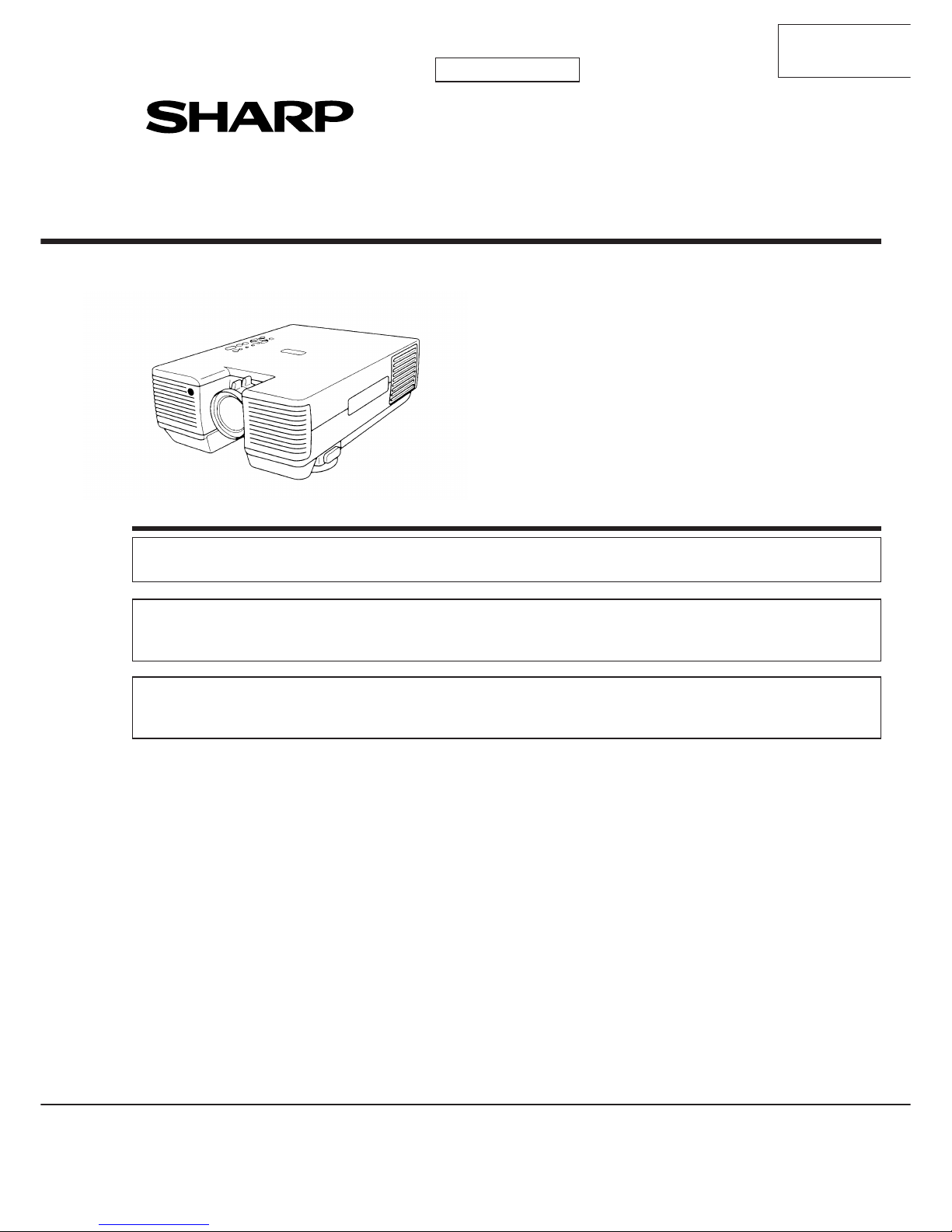
XG-NV1E
XG-NV1EA
SHARP CORPORATION
SERVICE MANUAL
SERVICE-ANLEITUNG
SECAM/PAL/NTSC SYSTEM
LCD PROJECTOR
LCD PROJEKTOR
Im lnteresse der Benutzersicherheit (erforderliche Sicherheitsregeln in einigen Ländern) muß das Gerät in seinen
Originalzustand gebracht werden. Außerdem dürfen für die spezifizierten Bauteile nur identische Teile verwendet
werden.
In the interests of user-safety (Required by safety regulations in some countries) the set should be restored to its original condition and only parts identical to those specified should be used.
MODELS
MODELLE
XG-NV1E
XG-NV1EA
TENTATIVE
Page 2
XG-NV1E
XG-NV1EA
2
CONTENS
Page
INHALT
Page
• OVERALL WIRING DIAGRAM.........................45
• DESCRIPTION OF SCHEMATIC DIAGRAM ...49
• WAVEFORMS .................................................. 50
• SCHEMATIC DIAGRAM................................... 51
• PRINTED WIRING BOARD ASSEMBLIES......89
• PARTS LIST
ELECTRICAL PARTS ................................. 99
CABINET AND MECHANICAL PARTS.....126
ACCESSORIES PARTS ........................... 134
PACKING PARTS ..................................... 135
• PACKING OF THE SET .................................136
• NOTE TO SERVICE PERSONNEL....................3
• SPECIFICATIONS.............................................. 4
• OPERATION MANUAL ...................................... 6
• REMOVAL OF MAJOR PARTS ........................ 11
• THE OPTICAL UNIT OUTLINE ........................ 16
• CONVERGENCE AND
FOCUS ADJUSTMENT.................................... 17
• ELECTRICAL ADJUSTMENT .......................... 21
• TROUBLESHOOTING T ABLE ......................... 22
• CHASSIS LAYOUT .......................................... 39
• BLOCK DIAGRAM ........................................... 41
• GESAMTSCHALTPLAN.......................................
• BESCHREIBUNG DES SCHEMATISCHEN
SCHALTPLANS....................................................
• WELLENFORMEN ...............................................
• SCHEMATISCHER SCHALTPLAN ......................
• LEITERPLATTENEINHEITEN..............................
• TEILELISTE
ELEKTRISCHE BAUTEILE ............................
CEHÄUSETEILE UND MECHANISCHE
TEILE..............................................................
ZUBEHÖRTEILE ............................................
VERPACKUNGSTEILE ..................................
• VERPACKEN DES GERÄTS ...............................
• HINWEISE FÜR DAS
WARTUNGSPERSONAL.....................................
• TECHNISCHE DATEN.........................................
• BEDIENUNGSANLEITUNG .................................
• ENTFERNEN DER WICHTIGSTEN TEILE..........
• ÜBERSICHT ÜBER DIE OPTIKEINHEIT.............
• ***** ......................................................................
• ELEKTRISCHE EINSTELLUNG...........................
• TABELLE FÜR STÖRUNGSSUCHE....................
• CHASSIS-ANORDNUNG.....................................
• BLOCKSCHALTBILD ...........................................
SeiteSeite
PagePage
• .............................................................................
• .............................................................................
• .............................................................................
• .............................................................................
• .............................................................................
•
........................................................................
........................................................................
........................................................................
........................................................................
• .........................................................................
• .............................................................................
• .............................................................................
• .............................................................................
• .............................................................................
• .............................................................................
• .............................................................................
• .............................................................................
• .............................................................................
•
• .............................................................................
Page 3
XG-NV1E
XG-NV1EA
3
NOTE TO SERVICE PERSONNEL
UV-RADIATION PRECAUTION
234567890123456789012345678901212345678901234567890123456789012123456789012345678901234567890121
2
234567890123456789012345678901212345678901234567890123456789012123456789012345678901234567890121
2
The light source, metal halide lamp, in the LCD
projector emits small amounts of UV-Radiation.
A VOID DIRECT EYE AND SKIN EXPOSURE.
To ensure safety please adhere to the following:
1. Be sure to wear sun-glasses when servicing the
projector with the lamp
turned “on” and the top
enclosure removed.
2. Do not operate the lamp outside of the lamp housing.
3. Do not operate for more than 2 hours with the
enclosure removed.
UV-Radiation and Medium Pressure
Lamp Precautions
1. Be sure to disconnect the AC plug when replacing
the lamp.
2. Allow one hour for the unit to cool down before
servicing.
3. Replace only with same type lamp. Type
CLMPF0042DE01 rated V/265W.
4. The lamp emits small amounts of UV-Radiation,
avoid direct-eye contact.
5. The medium pressure lamp involves a risk of
explosion. Be sure to follow installation instructions
described below and handle the lamp with care.
DANGER ! –– Never turn the power on without
the lamp to avoid electric-shock or damage of the
devices since the stabilizer generates high voltages
at its start.
Lamp Replacement
Note:
Since the lamp reaches a very high temperature
during units operation replacement of the lamp should
be done at least one hour after the power has been
turned off. (to allow the lamp to cool off.)
Installing the new lamp, make sure not to touch the
lamp (bulb) replace the lamp by holding its reflector
2.
[Use original replacement only.]
1
2
Lamp
Reflector
Page 4
XG-NV1E
XG-NV1EA
4
Page 5
XG-NV1E
XG-NV1EA
5
Page 6
XG-NV1E
XG-NV1EA
6
Page 7
XG-NV1E
XG-NV1EA
7
Page 8
XG-NV1E
XG-NV1EA
8
Page 9
XG-NV1E
XG-NV1EA
9
Page 10
XG-NV1E
XG-NV1EA
10
Page 11
XG-NV1E
XG-NV1EA
11
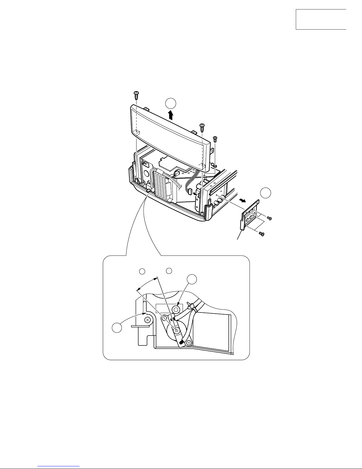
REMOVING OF MAJOR PARTS
Before starting this job, detach the lamp cage unit and the filter cover.
1.Removing the top cabinet
1-1. Remove the three screws at the carrying handle side.
1-2. Remove the two screws at the terminals side.
1-3. Detach the terminal door, and remove the four screws off the terminal cover.
1-4. Slowly lift the back of the top cabinet and disconnect the operation key unit connector (KY). Pull up and
away the top cabinet.
1-5. Place the top cabinet upside down. Remove the four screws off the operation key unit. Take out the
operation key unit.
(KY)
1-2
1-4
1-3
1-2
Top Cabinet
Terminal Door
1-1
Page 12
XG-NV1E
XG-NV1EA
12
2.Removing the front cabinets
2-1. Tilt the front-right cabinet forward. Pull it up out of position.
2-2. Tilt the front-left cabinet forward. Disconnect the infrared R/C receiver unit. Pull up the cabinet out of
position.
2-2
2-1
Front-right Cabinet
Infrared R/C Receiver Unit
Front-left Cabinet
Page 13
XG-NV1E
XG-NV1EA
13
3.Removing the rear cabinet and video terminal cover
3-1. Remove the two screws off the rear cabinet and the screw from the static ground lead. Pull up the cabinet
and disconnect the speaker connector (SP). Now the rear cabinet is free.
3-2. Remove the four screws off the video terminal cover. Detach the cover.
(SP)
3-1
3-2
a
b
Video Terminal Cover
Boss
Rib
Make sure the bimetal lead terminals are at the bottom
of the boss a and rib b .
Rear Cabinet
Page 14
XG-NV1E
XG-NV1EA
14
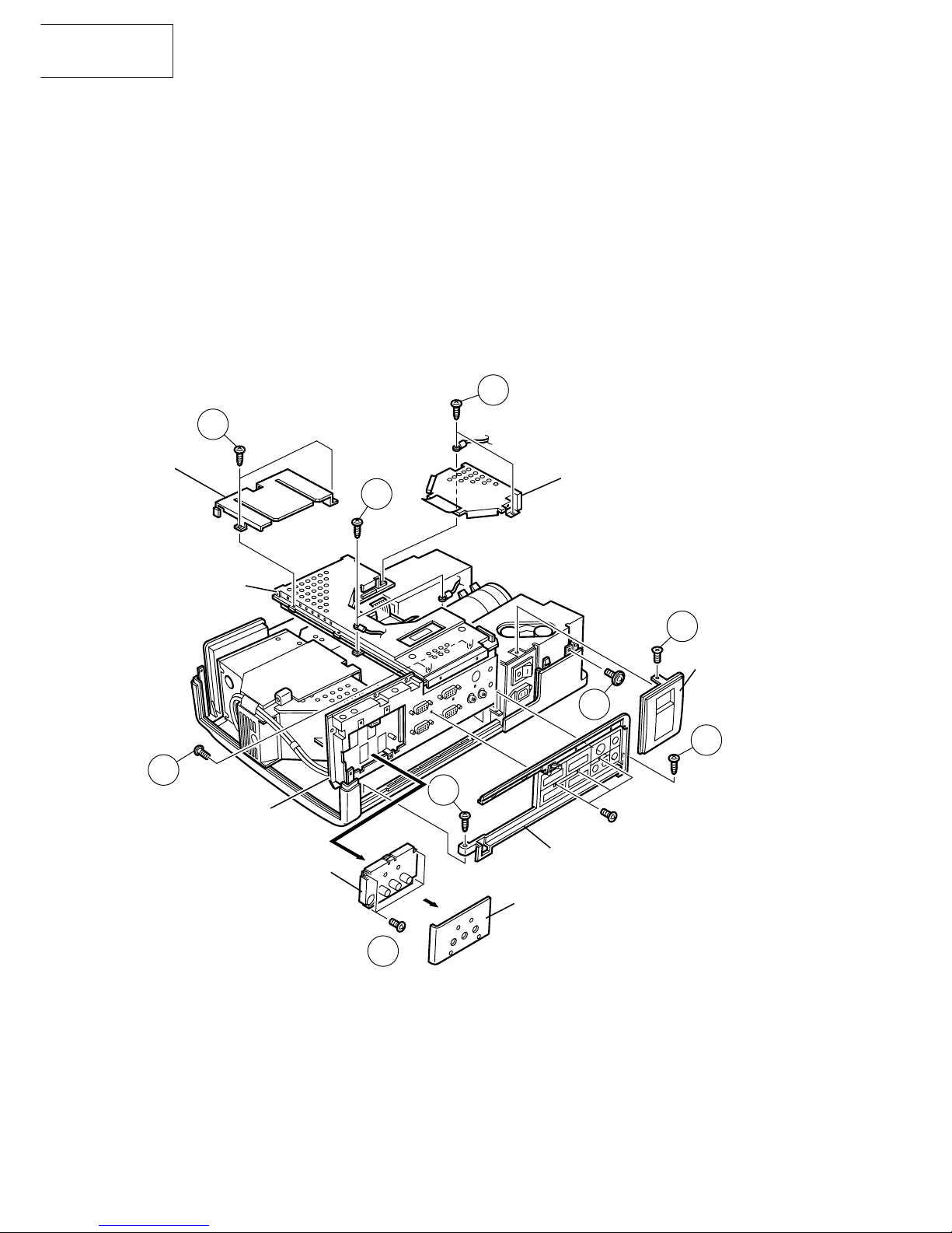
4.Removing the PWBs
4-1. Remove the two screws that fix the PC terminal cover to the bottom cabinet.
4-2. Remove the two screws off the output shield. Take out the output shield and disconnect the R-LCD, G-LCD
and B-LCD connectors (RP, GP, and BP).
4-3. Remove the four screws off the output unit. Disconnect the insulating barrier, the ground leads and the
connectors (FN, Q, LL, FF , LF, BL, RC and EA). Pull up and away the output unit and the signal/PC terminal/
video board unit.
4-4. Peel off the shield sheet. Remove the four screws off the video board unit. Pull the unit toward yourself to
take it out.
4-5. Remove the two screws off the back of the output unit. Separate this unit from the signal/PC terminal unit.
4-6. Remove the screw off the bottom cabinet and the screw off the power panel. Now take out the power panel.
4-1
4-1
4-3
4-3
4-2
4-5
4-4
4-6
4-6
Insulating
Barrier
Output Unit
Signal/PC Terminal
Unit
Output Shield
Power Panel
PC Terminal Cover
Shield Plate
Video Board
Unit
Page 15
XG-NV1E
XG-NV1EA
15
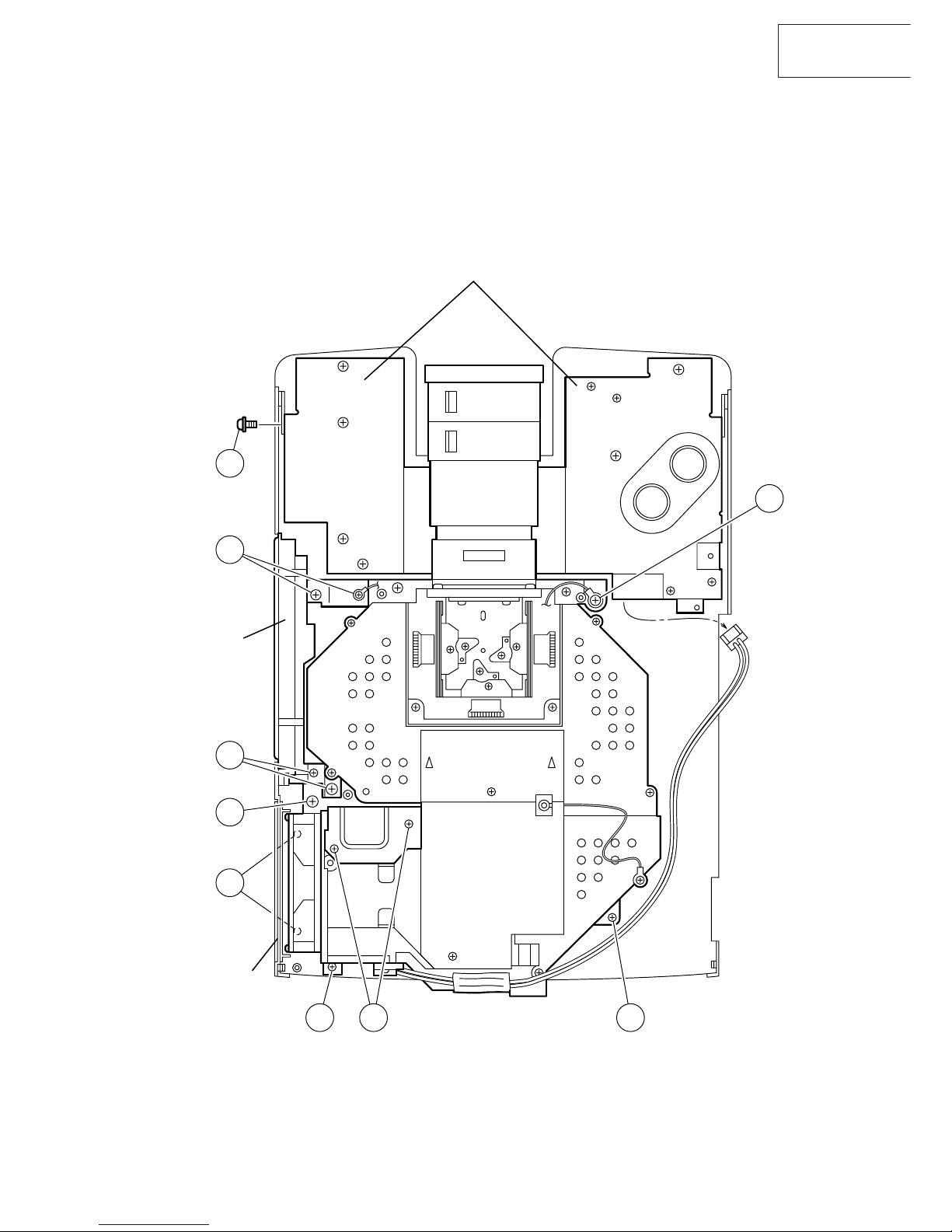
5.Removing the optics mechanism assembly
5-1. Remove the two screws off the angles A and B of the carrying handle. Detach the carrying handle.
5-2. Remove the two screws off the lamp socket holder. Take out the lamp socket.
5-3. Disconnect the bimetal connector (BA). Remove the four screws off the optics mechanism assembly, and
pull up and away this assembly.
5-4. Remove the two screws off the exhaust panel. Separate the panel from the bottom cabinet.
5-5. Remove the screw off the power/ballast unit assembly. Pull up and away the unit.
5-1
5-5
5-1
5-3
5-3 5-2 5-3
(BA)
5-3
5-4
Power/Ballast Unit
Carrying
Handle
Optics
Mechanism
Ass'y
Exhaust
Panel
Page 16
XG-NV1E
XG-NV1EA
16
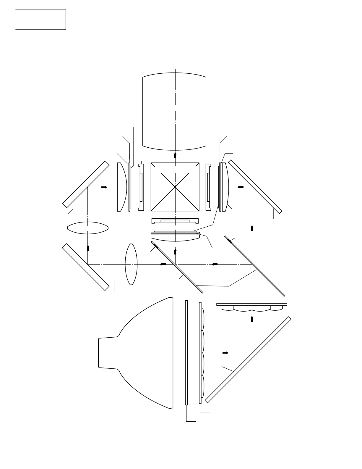
B-LCD
G-LCD
GREEN
BLUE
BLUE
RED
R-LCD
Polarizer film
Dichroic coating
(B transmission)
Dichroic coating
(B reflection)
Incident polarizer plate R
Dichroic coating
(R transmission)
AL-coated mirror R
AL-deposited face
Polarizer film
Marking
AR-coated face
Marking
G reflector
Dichroic coating
B/G reflector
AL-coated mirror W
AL-deposited
face
Fly-eye lens (incoming light)
UV cut filter
Metal-halide lamp
(Light source)
Relay lens 1
AL-deposited face
AL-coated mirror B
Projection Lens
B reflector
Cross dichroic prism
Incident polarizer plate B
Relay lens 3
Relay lens 2
Incident polarizer plate G
Condenser lens G
Fly-eye lens (outgoing light)
Condenser lens R
* M3
M6
M4
M2
M5
M1
THE OPTICAL UNIT OUTLINE
* The M3 mirrors have a coating
wedge (for different film thickness). Set up these mirrors, with
their markings positioned as
shown above, so that their
coated faces and both sides be
in the correct directions.
Layout of the optical system
Note: Layout for positioning the optical system.
Page 17

XG-NV1E
XG-NV1EA
17
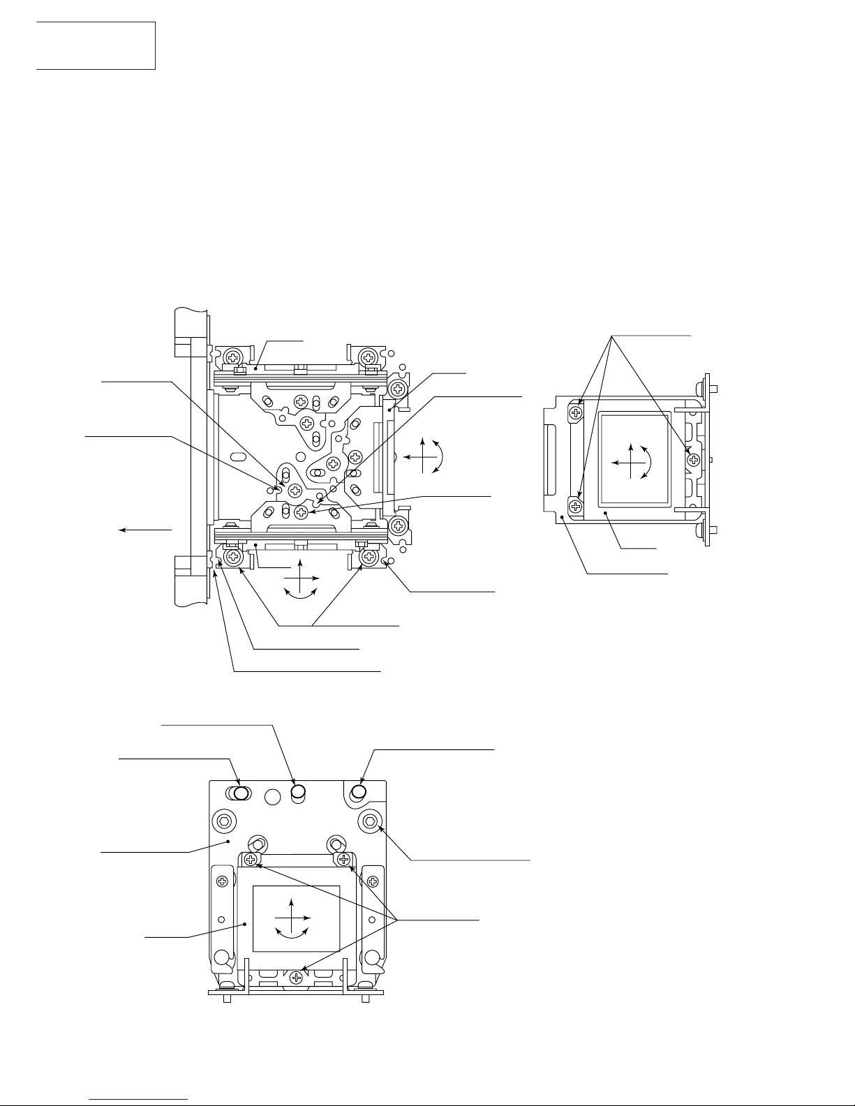
CONVERGENCE AND FOCUS ADJUSTMENT
» Start the convergence and focus adjustments with the top cabinet and the signal
shield removed but the power on. Use the remote control gun to adjust the image.
Take the following procedures.
1. Focusing the projection lens
(A) Replacing all the 3 LCD panels
1. Before replacing all the 3 LCD panels, project an image on the screen and bring it into focus.
2. Replace the panels with new ones. But until the focus has been completely readjusted, be careful not to
change the distance between the set and the screen, nor to move the projection lens focus and zoom
rings.
If the focus is readjusted with a different positional relation, the relation between the projection distance
and the screen size is affected. In other words, a short-distance image (40 WIDE, for example) may
get out of the focus range, or a long-distance image (300 WIDE, for example) may come out of focus.
(B) Replacing 1 or 2 of the 3 LCD panels
1. In adjusting the focus after replacement of one or two LCD panels, project an image on the screen and
turn the projection lens focus ring to get the non-replaced LCD panel into focus.
2. But until the focus has been completely adjusted for the new LCD panels, be careful not to change the
distance between the set and the screen, nor to move the projection lens focus and zoom rings.
(If the distance has been changed or the projection lens readjusted, repeat the above steps 1 and 2.)
2. Adjusting the G-LCD panel
(A) Focus adjustment. (Make this adjustment on the white-only screen.)
1. Right-and-left focus adjustment (θY direction) . Loosen the lock screws "b" and "c" and insert the eccentric
screwdriver into the notch and hole "b". Turn the screwdriver until the right and left halves on the screen
get into focus.
First get the right and left halves in balance. Then improve the accuracy while making the adjustment
2 below.
2. T op-center-bottom focus adjustment (θX and Z directions). Loosen the lock screws "a" and "c" and insert
the eccentric screwdriver into the notch and hole "a" or "c".
Turn the screwdriver until the top, center and bottom on the screen get into focus. In adjusting this topto-bottom focus, temporarily tighten the lock screw "b" to fix the θY direction adjustment.
3. Repeat the above steps 1 and 2 to finely adjust the focus. Finally tighten up all the lock screws.
Note :
1 Carefully proceed with the focus adjustment because the adjusting directions are correlated.
2 In adjusting the convergence and focus, do not move the projection lens zoom and focus rings until the
end of all the adjustments.
(B) Convergence adjustment
» The G-LCD panel has no convergence adjustment mechanism. Use this panel as convergence adjustment
reference.
3. B-LCD panel adjustment (the same for the R-LCD panel)
(A) Focus adjustment
» Take the same procedure as for the G-LCD panel focus adjustment. Note that the adjustment range is
small in the Z direction. If the convergence is quite different between the B-LCD and G-LCD panels,
roughly adjust the convergence first and then the focus.
(B) Convergence adjustment
» Use a crosshatch pattern signal for this adjustment.
Make the adjustment just for the G-colour and the relevant colour.
(1) Loosen the convergence lock screw "d".
(2) With the G-LCD panel’s screen center as reference, adjust the B-LCD panel in the X, Y and θZ directions.
(3) Finally tighten up the convergence lock screw "d".
)
(
)
(
Page 18
XG-NV1E
XG-NV1EA
18
X
Z
θY
X
Y
θZ
X
Y
θZ
X
Z
θY
Notch and hole "a"
(Use an eccentric
screwdriver.)
Notch and hole "b"
(Use an eccentric
screwdriver.)
Lock screw "b"
(θY direction)
G-LCD panel
mounting screws
G adjusting plate
Notches and
holes "c"
(Use on eccentric
screwdriver.)
Notches and holes "c"
Lock screws "c"
(Use an bladed screwdriver.)
Eccentric cam
(Y direction adjustment)
Eccentric cam
(X direction adjustment)
Eccentric cam
(θZ direction adjustment)
Lock screw "d"
(convergence adjustment)
R•B adjusting plate
R•B-LCD
R•B-LCD panel
mounting screws
TOP VIEW
SIDE VIEW
SIDE VIEW
Lock screw "a"
FRONT
R-LCD
G-LCD
B-LCD
G-LCD
Convergence and Focus Adjustments Mechanism
Note :
1 The eccentric cam is used for convergence adjustment. This means that the cam’s turning and the linear
movement are not always uniform.
2 This model is not equipped with the LCD image adjustment mechanism. This is because the dichroic
prism is used for image formation. When the LCD panels all get into the best focus, the images are
almost completely converged.
Page 19
XG-NV1E
XG-NV1EA
19
X direction LCD right and left
Convergence Y direction LCD top and bottom
θZ direction Rotation around Z axis LCD turning axis
Z direction LCD optical axis
Focus θX direction Rotation around X axis LCD top-to-bottom flapping
θY direction Rotation around Y axis LCD right-to-left flapping
Tool Specific or General Tool code Configuration
Eccentric cam Specific 9DASPN-XGNV1U
adjusting wrench
Eccentric screwdriver Specific 9EQDRiVER-NV1A
Hex wrench General (redesigned) 9EQLNC-XGNV1U
Bladed screwdriver General 9EQDRiVER-NV1B
Phillips screwdriver General — For M2.6 pan-head machine screw
0.5
85min
ø5
(ø3.5)
3.5
2
5
(16)
(R2)
(50)
CUT
100
80
Focus Adjustments the Other Way
a Notch and hole "a" Z and θX directions
b Notch and hole "b" θY direction
c Notch and hole "c" Z, θX and θY directions
Convergence and Focus Adjusting and Tightening Tools
X direction ±0.8mm Eccentric cam Eccentric cam adjusting wrench d Hex wrench
Convergence Y direction ±0.8mm Eccentric cam Eccentric cam adjusting wrench d Hex wrench
R/B θZ direction ±1° Eccentric cam Eccentric cam adjusting wrench d Hex wrench
colours Z direction 0.8mm
Notch and hole "a" & "c"
Eccentric screwdriver, a, c Phillips
Focus θX direction ±1°
Notch and hole "a" & "c"
Bladed screwdriver a, c screwdriver
θY direction ±1°
Notch and hole "b" & "c"
b, c
Z direction ±0.2mm
G colour Focus θX direction ±1° Same as for R and B colours
θY direction ±1°
Colour Adjustment Direction
Movement
Position Adjusting tool
Lock screw
Tightening tool
Convergence and Focus Adjustments at a Glance
Adjustment directions
Lock screw Position Related direction
Adjustment Direction Definition Direction of LCD panel
Convergence and Focus Adjustment for the XG-NV1 Optical Mechanism
Page 20
XG-NV1E
XG-NV1EA
20
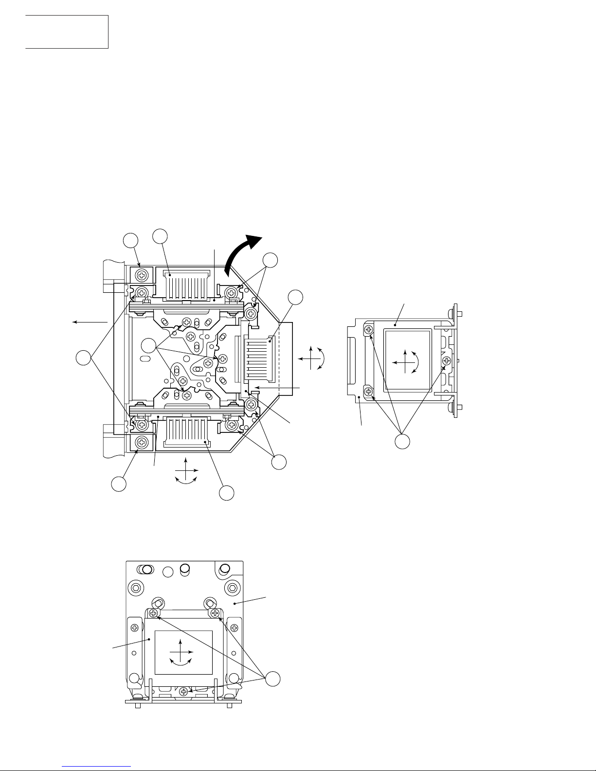
Replacing the LCDs
With the top cabinet removed
(1)Remove the output shield.
(2)Disconnect the LCD flat cable from the output PWB connector.
(3)Remove the lock screws "b" and "c". Detach the R/B adjusting plate or the G adjusting plate together with the
LCD panel.
(4)Separate the LCD panel from the adjusting plate.
(5)Mount a new LCD panel in the reverse order of the above steps (1), (2), (3) and (4).
~ Readjust the convergence and focus. Note that the G LCD panel needs no convergence adjustment and has
a small adjustment range in the Z direction.
X
Z
θY
TOP VIEW
SIDE VIEW
SIDE VIEW
X
Z
θY
X
Y
θZ
X
Y
θZ
G-LCD panel
mounting screws
G adjusting plate
Lock screws "c"
Lock screws "c"
Lock
screws "c"
Lock
screws "b"
R•B adjusting plate
R•B-LCD
R•B-LCD panel
mounting screws
FRONT
R-LCD
B-LCD
~
G-LCD
G-LCD
1
1
4
4
2
2
2
3
3
3
3
Page 21

XG-NV1E
XG-NV1EA
21
ELECTRICAL ADJUSTMENT
NOTE : The settings have been factory-adjusted to their best points. If any of them gets out of spec or after any
relevant part has been replaced, make the related adjustment.
Step
Adjustment Position
Adjustment Conditions Adjustment Method
Destinations Factory setting Setting on
remote control
Export S4 Set to 4 on shipment
Domestic S5 Set to 5 on shipment
1 Initialization of
EEPROM
2 Off-set for RGB
input
3 RGB gain
4 R-drive
5 B-drive
6 Rough-adjustment
of the voltage for
white
7 Rough-adjustment
of the voltage for
black
8 White balance
9 Common DC bias
1.Turn on the unit (Lighting
lamp) and burn-in for 15
minutes.
1. Supply the black signal.
(APL=100%)
2. Push S5013 then appearing ADJ-IN mode.
3. Select RGB1.
1. Supply the green (100%)
signal.
2. Select RGB1.
1. Supply the red (100%) signal
2. Select RGB1
1. Supply the blue (100%) signal.
2. Select RGB1.
1. Select RGB2.
1. Select RGB2.
1. Supply the gray scale signal1.
2. Select RGB2.
3. Items to be adjusted
· RW/RB
· GW/GB
· BW/BB
1. Supply each individual signal of R, G and B.
2. Select RGB2.
» Adjust ROS→128
GOS→128
BOS→128
» Adjust GAIN→62
» Adjust R-DRIVE→128
» Adjust B-DRIVE→128
» Adjust RW→60
GW→60
BW→60
» Adjust RB→196
GB→196
RB→196
» Should be adjusted to keep the following value.
RW+RB=256
GW+GB=256
BW+BB=256
» Adjust RC (Red), GC (Green) and BC (Blue) to obtain
the maximum contrast with each colour.
» Set as follows
Page 22

XG-NV1E
XG-NV1EA
TROUBLE SHOOTING TABLE (Continued)
22
Checking the PWB performance
Use specified cable.
No
No
No
No
No
No
No
No
Yes
Yes
Yes
Yes
Yes
Yes
Yes
Yes
Yes
RGB input in trouble
Feed test pattern signal from PC.
Is supply voltage as specified?
Does image appear?
Is the image proper?
Does G picture appear?
Does R picture appear?
Is specified cable connected between
PC and projector?
Check control circuit (IC5001, IC5002,
IC5003 and IC5010).
Are D/A outputs of IC1007, IC1008
and IC1030 as specified?
Go to "Checking the B signal line of
output PWB".
Through-output in trouble
Power circuit in trouble.
Go to "Checking the through-output
circuit".
Are D/A outputs of IC1003, IC1004
and IC1028 as specified?
Go to "Checking the G signal line of
output PWB".
Are D/A outputs of IC1005, IC1006
and IC1029 as specified?
Go to "Checking the R signal line of
output PWB".
Go to "Checking the B signal line of
signal processing PWB".
Go to "Checking the remote control
circuit".
Go to "Checking the G signal line of
signal processing PWB".
Go to "Checking the R signal line of
signal processing PWB".
Remote control in trouble
TROUBLE SHOOTING TABLE
Page 23

XG-NV1E
XG-NV1EA
TROUBLE SHOOTING TABLE (Continued)
23
Yes
Checking the G signal line of signal processing PWB
No
No
Yes
No
No
No
No
No
Yes
Yes
Yes
Yes
Yes
No
Yes
Yes
Yes
No
No
Yes
No
Yes
No
No
No
No
Yes
Yes
Yes
Go to "Checking synchronization".
Go to "Checking synchronization".
Check IC1002 and its peripheral parts.
IC1012, IC5002 or nearby circuit in
trouble.
IC1009 or nearby circuit in trouble.
IC1201 or nearby circuit in trouble.
Is there signal input at pin (11) of
IC1011?
Is there signal output at pin (35) of
IC1011?
Is there signal input at pin (7) of
IC1015?
Are there signal outputs at pins (197)
thru (204) of IC1201?
Is there clock output at pin (233) of
IC1001?
IC1003, IC1004, IC1028 or nearby
circuit in trouble.
Is there sync signal input at pins (15),
(216) or (217) of IC1201?
Are there signal inputs at pins (1),
(2), (3), (5) thru (8), (127) thru (130),
(132) thru (136), (138), (139), (145)
thru (149), (151) thru (154), (156)
thru (160) of IC1206?
Are there signal inputs at pins (143),
(144), (146), (147), (148), (152) and
(154) of IC1001?
Are there signal outputs at CH10 thru
CH17, CH20 thru CH27, CH30 thru
CH37, CH40 thru CH47, CH50 thru
CH57, and CH60 thru CH67 of
IC1001?
Check pin (4) line of connector TN.
Do voltages at pins (6), (18) and (19)
of IC1012 change?
Is there HSYNC signal input at pin
(23) of IC1011?
Is there clock input at pin (94) of
IC1001?
IC1011 or nearby circuit in trouble.
IC1015 or nearby circuit in trouble.
Is there clock output at pin (14) of
IC1201?
IC1001 or nearby circuit in trouble.
IC1206 or nearby circuit in trouble.
Is there clock input at pin (49) of
IC1201?
IC1001 or nearby circuit in trouble.
Are there clock inputs at pins (60),
(103) and (143) of IC1206?
Page 24

XG-NV1E
XG-NV1EA
TROUBLE SHOOTING TABLE (Continued)
24
Yes
Checking the R signal line of signal processing PWB
No
No
Yes
No
No
No
No
No
Yes
Yes
Yes
Yes
Yes
No
Yes
Yes
Yes
No
No
Yes
No
Yes
No
No
No
No
Yes
Yes
Yes
Go to "Checking synchronization".
Go to "Checking synchronization".
Check IC1002 and its peripheral parts.
IC1012, IC5002 or nearby circuit in
trouble.
IC1009 or nearby circuit in trouble.
IC1201 or nearby circuit in trouble.
Is there signal input at pin (7) of
IC1011?
Is there signal output at pin (40) of
IC1011?
Is there signal input at pin (7) of
IC1014?
Are there signal inputs at pins (189)
thru (196) of IC1201?
Is there clock output at pin (233) of
IC1001?
IC1003, IC1004, IC1028 or nearby
circuit in trouble.
Is there sync signal input at pins (15),
(216) or (217) of IC1201?
Are there signal outputs at pins (1),
(2), (3), (5) thru (8), (127) thru
(130), (132) thru (136), (138), (139),
(145) thru (149), (151) thru (154),
(156) thru (160) of IC1206?
Are there signal outputs to pins
(129), (131), (132), (133), (136),
(137), (138) and (142) of IC1001?
Are there signal outputs at CH10 thru
CH17, CH20 thru CH27, CH30 thru
CH37, CH40 thru CH47, CH50 thru
CH57, and CH60 thru CH67 of
IC1001?
Check pin (4) line of connector TN.
Do voltages at pins (5), (18) and (19)
of IC1012 change?
Is there HSYNC signal input at pin
(23) of IC1011?
Is there clock input at pin (94) of
IC1001?
IC1011 or nearby circuit in trouble.
IC1015 or nearby circuit in trouble.
Is there clock output at pin (14) of
IC1201?
IC1001 or nearby circuit in trouble.
IC1206 or nearby circuit in trouble.
Is there clock input at pin (49) of
IC1201?
IC1001 or nearby circuit in trouble.
Are there clock inputs at pins (60),
(103) and (143) of IC1206?
Page 25

XG-NV1E
XG-NV1EA
TROUBLE SHOOTING TABLE (Continued)
25
Yes
Checking the B signal line of signal processing PWB
No
No
Yes
No
No
No
No
No
Yes
Yes
Yes
Yes
Yes
No
Yes
Yes
Yes
No
No
Yes
No
Yes
No
No
No
No
Yes
Yes
Yes
Go to "Checking synchronization".
Go to "Checking synchronization".
Check IC1002 and its peripheral parts.
IC1012, IC5002 or nearby circuit in
trouble.
IC1009 or nearby circuit in trouble.
IC1201 or nearby circuit in trouble.
Is there signal input at pin (15) of
IC1011?
Is there signal output at pin (30) of
IC1011?
Is there signal input at pin (7) of
IC1016?
Are there signal outputs at pins (205)
thru (208), (212) thru (215) of IC1201?
Is there clock output at pin (233) of
IC1001?
IC1003, IC1004, IC1028 or nearby
circuit in trouble.
Is there sync signal input at pins (15),
(216) or (217) of IC1201?
Are there signal outputs at pins (1),
(2), (3), (5) thru (8), (127) thru (130),
(132) thru (136), (138), (139), (145)
thru (149), (151) thru (154), (156)
thru (160) of IC1206?
Are there signal outputs at pins
(156), (157), (158), (162), (163),
(164), (166) and (167) of IC1001?
Are there signal outputs at CH10 thru
CH17, CH20 thru CH27, CH30 thru
CH37, CH40 thru CH47, CH50 thru
CH57, and CH60 thru CH67 of
IC1001?
Check pin (4) line of connector TN.
Do voltages at pins (7), (18) and (19)
of IC1012 change?
Is there HSYNC signal input at pin
(23) of IC1011?
Is there clock input at pin (94) of
IC1001?
IC1011 or nearby circuit in trouble.
IC1015 or nearby circuit in trouble.
Is there clock output at pin (14) of
IC1201?
IC1001 or nearby circuit in trouble.
IC1206 or nearby circuit in trouble.
Is there clock input at pin (49) of
IC1201?
IC1001 or nearby circuit in trouble.
Are there clock inputs at pins (60),
(103) and (143) of IC1206?
Page 26

XG-NV1E
XG-NV1EA
TROUBLE SHOOTING TABLE (Continued)
26
Checking the G signal line of output PWB
No
Yes
Connector CC poorly soldered or in
trouble.
Are outputs at pins (3), (4) and (5) of
IC4034 as specified?
Are there signal inputs at pins (1)
each of IC4038 thru IC4043?
Check connector CC. Do signals go
to pins (4), (5), (7), (8), (10) and (11)
of this connector?
IC4034, IC5002 or nearby circuit in
trouble.
Yes
Are there signal outputs at pins (7),
(8) and (14) of IC4044 and IC4045?
IC4038 thru IC4043, IC4044, IC4045
or nearby circuit in trouble.
Yes
Are signals fed from pins (2) thru (7)
of connector GP to the panel?
Connector GP poorly soldered or in
trouble.
Yes
Does flicker happen?
Go to "Checking the image for
shifting".
Yes
Is frame pulse fed to pin (1) of
connector GP?
Yes
Is common bias at pin (24) of
connector GP as specified?
Yes
Panel in trouble.
Yes
Yes
Q4024, Q4025, Q4026 or their signal
line in trouble.
Does frame pulse go out of IC4077?
Yes
Are FRP1 and FRP2 signals fed to
pins (9) and (12) of IC4077?
Any of IC4038 thru IC4043 faulty.
Checking the image for shifting
Yes Yes
IC1001 or nearby circuit in trouble.
Are signals fed via IC4074, IC4075
and IC4076 to the panel?
Panel in trouble.
Are signals fed to IC4074, IC4075
and IC4076?
IC4074, IC4075, IC4076 or nearby
circuit in trouble.
IC4077 or nearby
circuit in trouble.
No
IC1001 or nearby
circuit in trouble.
No
No
No
No
No
No No
No
No
Page 27

XG-NV1E
XG-NV1EA
TROUBLE SHOOTING TABLE (Continued)
27
Checking the R signal line of output PWB
No
Yes
Connector CC poorly soldered or in
trouble.
Are outputs at pins (2), (18) and (19)
of IC4034 as specified?
Are there signal inputs at pins (1)
each of IC4401 thru IC4406?
Check connector CC. Do signals go
to pins (13), (14), (16), (17), (19) and
(20) of this connector?
IC4034, IC5002 or nearby circuit in
trouble.
Yes
Are there signal outputs at pins (7),
(8) and (14) of IC4036 and IC4407?
IC4401 thru IC4406, IC4436, IC4407
or nearby circuit in trouble.
Yes
Are signals fed from pins (2) thru (7)
of connector RP to the panel?
Connector RP poorly soldered or in
trouble.
Yes
Does flicker happen?
Go to "Checking the image for
shifting".
Yes
Is frame pulse fed to pin (1) of
connector RP?
Yes
Is common bias at pin (24) of
connector RP as specified?
Yes
Panel in trouble.
Yes
Yes
Q4024, Q4025, Q4026 or their signal
line in trouble.
Does frame pulse go out of IC4077?
Yes
Are FRP1 and FRP2 signals fed to
pins (9) and (12) of IC4077?
Any of IC4401 thru IC4406 faulty.
IC4077 or nearby
circuit in trouble.
No
IC1001 or nearby
circuit in trouble.
No
No
No
No
No
No
No
Page 28

XG-NV1E
XG-NV1EA
TROUBLE SHOOTING TABLE (Continued)
28
Checking the B signal line of output PWB
No
Yes
Connector CC poorly soldered or in
trouble.
Are outputs at pins (6), (7) and (8) of
IC4034 as specified?
Are there signal inputs at pins (1)
each of IC4001 thru IC4006?
Check connector CC. Do signals go
to pins (22), (23), (25), (26), (28) and
(29) of this connector?
IC4034, IC5002 or nearby circuit in
trouble.
Yes
Are there signal outputs at pins (7),
(8) and (14) of IC4007 and IC4008?
IC4001 thru IC4006, IC4007, IC4008
or nearby circuit in trouble.
Yes
Are signals fed from pins (2) thru (7)
of connector BP to the panel?
Connector BP poorly soldered or in
trouble.
Yes
Does flicker happen?
Go to "Checking the image for
shifting".
Yes
Is frame pulse fed to pin (1) of
connector BP?
Yes
Is common bias at pin (24) of
connector BP as specified?
Yes
Panel in trouble.
Yes
Yes
Q4024, Q4025, Q4026 or their signal
line in trouble.
Does frame pulse go out of IC4077?
Yes
Are FRP1 and FRP2 signals fed to
pins (9) and (12) of IC4077?
Any of IC4001 thru IC4006 faulty.
IC4077 or nearby
circuit in trouble.
No
IC1001 or nearby
circuit in trouble.
No
No
No
No
No
No
No
Page 29

XG-NV1E
XG-NV1EA
TROUBLE SHOOTING TABLE (Continued)
29
Checking synchronization
No
No
Yes
Yes
Yes
No
Are there signal outputs at pins
(3)(IN+) of IC2003 and IC2004?
Are there signal outputs at pins
(15)(H) and (217)(V) of IC1201?
Do horizontal and vertical sync
signals (at pins (13) and (14) of RGB
connector) come out of PC?
Are there signal outputs at pins
(6)(X1/EXT) and (22)(EXFBK) of
IC1013?
Connector or nearby circuit in trouble.
Go to "Checking the PLL circuit".
IC2003, IC2004 or nearby circuit in
trouble.
No
Yes
Yes
No
Is there signal output at pin (3)(IN+)
of IC2005?
Is there signal output at pin (216)(C)
of IC1201?
Connector or nearby circuit in trouble.
Go to "Checking the PLL circuit".
IC2005 or nearby circuit in trouble.
No
Yes
Yes
No
Is there signal output at pin
(15)(DOTCLK) of IC1013?
Check the sync circuit and its
peripheral parts.
IC1201 or nearby circuit in trouble.
IC1013, IC1201 or nearby circuit in
trouble.
Checking the PLL circuit
Page 30

XG-NV1E
XG-NV1EA
TROUBLE SHOOTING TABLE (Continued)
30
Checking the remote control circuit
Yes
No
IC5001, IC5101, IC5102 or nearby
circuit in trouble.
Press the MENU key. Are there
signal outputs at pins (29) and (30) of
connector CA?
Remote control receiver or its nearby
circuit in trouble.
Checking the through-output circuit
Yes
No
Yes
No
Is specified cable connected between
LCP and monitor?
Yes
No
IC2003, IC2004, IC2005 or nearby
circuit in trouble.
Does analog output come from PC?
No digital output.
Use specified cable.
Are LCP and monitor in sync?
IC2001 or nearby circuit in trouble.
Page 31

XG-NV1E
XG-NV1EA
TROUBLE SHOOTING TABLE (Continued)
31
No
X6001 or nearby circuit in trouble.
No
No
Lamp fails to light up.
Checking the video system
Are there signal inputs at pins (183),
(189) thru (204), (214) and (215) of
IC1201?
Yes
No picture
Is lamp on?
Is voltage applied to connector EA?
Is X6001 oscillating?
Yes
Yes
No
Are there signal inputs at pins (15),
(17) and (19) of IC6001?
Check signal line circuit.
Check power circuit and its parts.
No
Connector VS in trouble.
IC6003, IC6004 or IC6005 in trouble.
IC1201 or nearby circuit in trouble.
Yes
Yes
No
Are there signal inputs at IC6003,
IC6004 and IC6005?
Yes
Is pin (26) of connector VS at "L"
level?
Check IC6001 and its peripheral
circuits.
Input switching in trouble IC5002 or
nearby circuit in trouble.
No
No
Yes
Are there signal outputs at IC6003,
IC6004 and IC6005?
Yes
Page 32

XG-NV1E
XG-NV1EA
TROUBLE SHOOTING TABLE (Continued)
32
No colour or unusual tint with NTSC signal
No
Yes
IC5001 or nearby circuit in trouble.
IC1201, IC1206 or nearby circuit in
trouble.
Set user control to standard value.
Check the video board.
Is colour mode judged properly?
Does user control work?
Video board in trouble.
Yes
Change process value for
adjustment.
Yes
No
No
No colour or unusual tint with PAL signal
No
Yes
IC5001 or nearby circuit in trouble.
IC1201, IC1206 or nearby circuit in
trouble.
Set user control to standard value.
Check the video board.
Is colour mode judged properly?
Does user control work?
Video board in trouble.
Yes
Change process value for
adjustment.
Replace the video board. Are colour
and tint as specified?
Yes
No
No
No colour or unusual tint with SECAM signal
No
Yes
IC5001 or nearby circuit in trouble.
IC1201, IC1206 or nearby circuit in
trouble.
Set user control to standard value.
Check the video board.
Is colour mode judged properly?
Does user control work?
Video board in trouble.
Yes
Change process value for
adjustment.
Replace the video board. Are colour
and tint as specified?
Yes
No
No
Replace the video board. Are colour
and tint as specified?
Page 33

XG-NV1E
XG-NV1EA
TROUBLE SHOOTING TABLE (Continued)
33
Yes
Yes
No synchronization
No
Yes
Yes
No
No
No
Check the signal line from IC6005.
Is there video signal input at pins (15),
(17) or (19) of IC6001?
Are HSYNC and VSYNC signals from
pins (41) and (42) of IC6001 in sync
with input signal?
Check IC6001 and its peripheral
circuits.
Check the signal line from the
connector.
Which of vertical and horizontal
syncs fails?
Is there signal input from pin (22) of
connector VS to pin (214) of IC1201?
Is there signal input from pin (20) of
connector VS to pin (215) of IC1201?
Check IC102 and its peripheral
circuits.
Vertical
Horizontal
Page 34

XG-NV1E
XG-NV1EA
TROUBLE SHOOTING TABLE (Continued)
34
Lamp failure to light up
No
No
Yes
Yes
Yes
Replace TGU1701. Check
connectors.
Is discharge noise heard?
No
Yes
Replace F701. Check and replace
Q1701.
Yes
Yes
Is F701 blown out?
No
Check DB701 and its peripheral parts.
No
Replace Q1702.
Yes
Is FET drive voltage applied from pin
(2) of IC1701?
No
IC1702 or nearby circuit in trouble.
Yes
No
Q1703 or nearby circuit in trouble.
Replace F704 or TF1701.
Is F704 or TF1701 blown out?
Yes
TGU1701 faulty.
Is voltage applied at TGU1701?
No
Is voltage applied to pin (16) of
IC1701?
Is voltage applied to pin (1) of
connector BL?
No
Check IC5001 and its peripheral
circuits.
Lamp faulty. Replace.
Does new lamp light up?
Is voltage applied across C1703?
Page 35

XG-NV1E
XG-NV1EA
TROUBLE SHOOTING TABLE (Continued)
35
No sound
Yes
No
Check IC302 and its peripheral
circuits.
Yes
No
Does voltage at pin (9) of IC301
change with VOL UP/DOWN keys?
IC305 or nearby circuit in trouble.
Yes
No
Are there audio signal inputs at pins
(2) and (23) of IC301?
IC306, IC1022, IC1023 or nearby
circuit in trouble.
Yes
No
Are there audio signal inputs at pins
(1) and (9) of IC304?
Yes
No
Are there audio signal inputs at pins
(1) and (3) of connector SP?
Is sound heard with 3D SOUND off?
IC307 or nearby circuit in trouble.
IC304 or nearby circuit in trouble.
Replace speaker.
Checking IC302 and its peripheral circuits
Yes
No
Are there signal inputs at pins (27)
and (28) of IC302?
IC306, C320, C321, R334, or related
part in trouble.
Yes
No
Are there signal outputs at pins (17)
and (18) of IC302?
IC302 or nearby circuit in trouble.
IC306, C344, C345, R357, R358 or
related part in trouble.
Page 36

XG-NV1E
XG-NV1EA
TROUBLE SHOOTING TABLE (Continued)
36
232C failure
Yes
No
Reconnect cable.
Yes
No
Is PC’s 232C setting as specified?
Make PC port setting.
Yes
No
Is there signal input at pin (11) of
IC2006?
Check cable, connector and their
peripheral parts.
Yes
No
Is there signal output at pin (12) of
IC2006?
Yes
No
Is there signal input at pin (47) of
IC5001?
Is cable connected?
IC2006 or nearby circuit in trouble.
Check signal line (connectors TH and
CA) and related parts.
IC5001 faulty.
Page 37

XG-NV1E
XG-NV1EA
TROUBLE SHOOTING TABLE (Continued)
37
Yes
Switch off the PC, select the remote
mouse, reconnect the cable, and get
the PC restarted.
Mouse failure
Yes
No
Is cable connected both with serial
port and PC-98?
Is OSD system check remote mouse
properly set?
(Pin (13) of IC200: AT = "L", 98 ="H")
Double connection unacceptable.
Set to AT except for PC-98.
Is CF2001 oscillating?
IC2007 or CF2001 in trouble.
IC1025 in trouble.
IC2007 faulty.
IC2007 faulty.
IC2008 faulty.
No
Is voltage applied to pin (5) of IC2007
and pin (8) of IC2008?
Power is supplied from pin (8) of
J2005 for AT and from pin (1) of
J2006 for PC-98. Recheck the cable.
Yes
No
Yes
No
Yes
No
Is there remote control signal input at
pin (8) of IC2007?
Yes
No
Is communication made with DAT at
pin (15) of IC2007 and CLK at pin(16)
of IC2007?
Yes
No
Click the mouse. Is pin (18)(BUTTON)
of IC2007 set to "H" level?
Yes
No
Is there signal output at IC2008?
PS/2: DATA at pin (24), CLOCK at
pin (25)
MAC: ADB OUT at pin (27), ADB IN
at pin (11)
98: XA at pin (14), XB at pin (15),
YA at pin (16), YB at pin (17),
RIGHT at pin (1), LEFT at pin
(2)
Page 38

XG-NV1E
XG-NV1EA
TROUBLE SHOOTING TABLE (Continued)
38
Memo
Page 39

H
G
F
E
D
C
B
A
123456789101112
XG-NV1E
XG-NV1EA
XG-NV1E
XG-NV1EA
CHASSIS LAYOUT
Ref. No.17
**
POWER/BALLAST UNIT–C
REDENC0228CEZC
REDENC0240CEZC
POWER/BALLAST UNIT–A
REDENC0228CEZA
REDENC0240CEZA
POWER/BALLAST UNIT–D
REDENC0228CEZD
REDENC0240CEZD
POWER/BALLAST UNIT–B
REDENC0228CEZB
REDENC0240CEZB
PC TERMINAL UNIT
RUNTK0568CEZZ
VIDEO BOARD UNIT
RUNTK0567CEZZ
RUNTK0584CEZZ
OPERATION KEY UNIT
RUNTK0566CEZZ
OUTPUT UNIT
DUNTK9292DE02/03/05
OUTPUT SUB UNIT
DUNTK9293DE02/03/05
SIGNAL UNIT
DUNTK9291DE02/03/05
R/C RECEIVER UNIT
DUNTK9295DE02/03/05
39 40
Page 40

H
G
F
E
D
C
B
A
123456789101112
XG-NV1E
XG-NV1EA
XG-NV1E
XG-NV1EA
BLOCK DIAGRAM-1
BALLAST
UNIT
POWER
UNIT
OPERATION
KEY UNIT
OUTPUT SUB
UNIT
OUTPUT UNIT
41 42
Page 41

H
G
F
E
D
C
B
A
123456789101112
XG-NV1E
XG-NV1EA
XG-NV1E
XG-NV1EA
43
BLOCK DIAGRAM-2
SIGNAL UNIT
VIDEO BOARD
UNIT
PC TERMINAL
UNIT
44
Page 42

H
G
F
E
D
C
B
A
123456789101112
XG-NV1E
XG-NV1EA
XG-NV1E
XG-NV1EA
OVERALL WIRING DIAGRAM-1
SIGNAL UNIT
OUTPUT UNIT
VIDEO BOARD UNIT
PC TERMINAL UNIT
45 46
Page 43

H
G
F
E
D
C
B
A
123456789101112
XG-NV1E
XG-NV1EA
XG-NV1E
XG-NV1EA
47
OVERALL WIRING DIAGRAM-2
OU PUT UNIT
OUTPUT SUB UNIT
CONTROL KEY UNIT
POWER/BALLAST UNIT
R/C RECEIVER UNIT
DUNTK9295DE02
DUNTK9295DE03
DUNTK9295DE05
48
Page 44

H
G
F
E
D
C
B
A
123456789101112
XG-NV1E
XG-NV1EA
XG-NV1E
XG-NV1EA
SC4001 (RP1)
H: 20µsec/div
V: 2V/div
1
SC4001 (RP2)
H: 20µsec/div
V: 2V/div
2
SC4001 (RP13)
H: 10µsec/div
V: 1V/div
3
SC4001 (RP14)
H: 0.1µsec/div
V: 1V/div
4
SC4001 (RP15)
H: 0.1µsec/div
V: 1V/div
5
SC4001 (RP21)
H: 10µsec/div
V: 1V/div
6
SC4001 (RP18)
H: 10µsec/div
V: 1V/div
7
SC4002 (GP2)
H: 20µsec/div
V: 2V/div
8
SC4003 (BP2)
H: 20µsec/div
V: 2V/div
9
P1402 (VS9, Y7)
H: 20µsec/div
V: 1V/div
0
P1402 (VS20, H-sync)
H: 20µsec/div
V: 1V/div
q
P1402 (VS22, V-sync)
H: 5msec/div
V: 1V/div
w
IC1003
(TP1101, 27-pin)
H: 10µsec/div
V: 500mV/div
e
IC1005
(TP1105, 27-pin)
H: 10µsec/div
V: 500mV/div
r
IC1007
(TP1109, 27-pin)
H: 10µsec/div
V: 500mV/div
t
VOLTAGE MEASUREMENT CONDITION:
1. Voltages at test points are measured at the supply voltage of AC 220V. Signals
are fed by a colour bar signal generator for servicing purpose and the above
voltages are measured with a 20-kohm/V tester.
WAVEFORM MEASUREMENT CONDI-TION:
1. Waveforms at test points are observed at the supply voltage of AC 220V.
Signals are fed by a colour bar signal generator for servicing purpose.
INDICATION OF RESISTOR & CAPACITOR:
RESISTOR
1. The unit of resistance “Ω” is omitted.
(K=kΩ=1000 Ω, M=MΩ).
2. All resistors are ± 5%, unless otherwise noted.
(J= ± 5%, F= ± 1%, D= ± 0.5%)
3. All resistors are 1/10W, unless otherwise noted.
4. All resistors are Carbon type, unless otherwise noted.
C : Solid W : Cement
S : Oxide Film T : Special
N : Metal Coating
DESCRIPTION OF SCHEMATIC DIAGRAM
CAPACITOR
1. All capacitors are µF, unless otherwise noted.
(P=pF=µµF).
2. All capacitors are 50V, unless otherwise noted.
3. All capacitors are Ceramic type, unless otherwise noted.
(ML): Mylar (TA): Tantalum
(PF): Polypro Film (ST): Styrol
CAUTION:
This circuit diagram is original one, therefore there may be a slight difference from yours.
SAFETY NOTE:
1. DISCONNECT THE AC PLUG FROM THE AC OUTLET BEFORE
REPLACEING PARTS.
2. SEMICONDUCTOR HEAT SINKS SHOULD BE REGARDED AS
POTENTIAL SHOCK HAZARDS WHEN THE CHASSIS IS OPERATING.
IMPORTANT SAFETY NOTICE:
PARTS MARKED WITH “å”( )ARE IMPORTANT FOR MAINTAINING
THE SAFETY OF THE SET. BE SURE TO REPLACE THESE PARTS WITH
SPECIFIED ONES FOR MAINTAINING THE SAFETY AND PERFORMANCE
OF THE SET.
SPANNUNGSMESSUNGEN:
1. Spannungen an den Prüfpunkten werden bei einer Netzspannung von 220V
gemessen, Signale werden für die Wartung mit einem Farbbalken-Signal
generator zugeführt, und Spannungen werden mit einem Meßinstrument
(20 k /V) ermittelt.
SIGNALFORMMESSUNGEN:
1. Die Wellenformen an den Testpunkten werden bei einer Netzspannung von
220V verfolgt. Signale werden für die Wartung mit einem Farbbalken-Signal
generator zugeführt.
BEZEICHNUNG DES WIDERSTANDS UND
KONDENSATORS:
WIDERSTAND
1. Die Widerstandseinheit “Ω” wird weggelassen.
(K=kΩ=1000 Ω, M=MΩ).
2. Alle Widerstände haben ± 5%, sofern nicht anders angegeben.
(J= ± 5%, F= ± 1%, D= ± 0.5%)
3. Alle Widerstände haben 1/10W, sofern nicht anders angegeben.
4. Alle Widerstände sind Kohletyp, sofern nicht anders angegeben.
C : Fest W : Zement
S : Oxidfilm T : Spezial
N : Metallüberzug
KONDENSATOR
1. Die Kapazitätseinheit ist µF, sofern nicht anders angegeben.
(P=pF=µµF).
2. Alle Kondensatoren haben 50V, sofern nicht anders angegeben.
3. Alle Kondensatoren sind Keramiktyp, sofern nicht anders angegeben.
(ML): Mylar (TA): Tantal
(PF): Polyprofilm (ST): Styrol
ACHTUNG:
bei diesem Schaltplan handelt es sich um den ursprünglichen. Esönnen
daher geringfügige Unterschiede zu dem lhrem bestehen.
SICHERHEITSANMERKUNGEN:
1. VOR DEM AUSWECHSELN VON TEILEN MUSS UNBEDINGT
NETZSTECKER AUS DER NETZSTECKDOSE GEZOGEN WERDEN.
2. DIE WARMEABLEITER DER HALBLEITER SOLLTEN BEIM BETRIEB
DES CHASSIS ALS MÖGLICHE URSACHEN VON GEFÄHRLICHEN
ELEKTRISCHEN SCHLÄGEN BETRACHTET WERDEN.
WICHTIGE SICHERHEITSANMERKUNGEN:
MIT “å”( )BEZEICHNETEN TEILE SIND BESONDERS WICHTIG
FÜR DIE AUFRECHTERHALTUNG DER SICHERHEIT . BEIM WECHDIESER
TEILE SOLLTEN DIE VORGESCHRIEBENEN TEILE IMMER VERWENDET
WERDEN, UM SOWOHL DIE SICHERHEIT ALS AUCH DIE LEISTUNG DES
GERÄTES AUFRECHTZUERHALTEN.
BESCHREIBUNG DES SCHEMATISCHEN SCHALTPLANS
WAVEFORMS
WELLENFORMEN
49 50
Page 45

H
G
F
E
D
C
B
A
123456789101112
XG-NV1E
XG-NV1EA
XG-NV1E
XG-NV1EA
SIGNAL UNIT-1/6
51 52
Page 46

H
G
F
E
D
C
B
A
123456789101112
XG-NV1E
XG-NV1EA
XG-NV1E
XG-NV1EA
SIGNAL UNIT-2/6
53 54
Page 47

H
G
F
E
D
C
B
A
123456789101112
XG-NV1E
XG-NV1EA
XG-NV1E
XG-NV1EA
55
SIGNAL UNIT-3/6
56
Page 48

H
G
F
E
D
C
B
A
123456789101112
XG-NV1E
XG-NV1EA
XG-NV1E
XG-NV1EA
SIGNAL UNIT-4/6
SIGNAL
SUB UNIT–A
57 58
Page 49

H
G
F
E
D
C
B
A
123456789101112
XG-NV1E
XG-NV1EA
XG-NV1E
XG-NV1EA
69 70
OUTPUT UNIT-3/5
Page 50

H
G
F
E
D
C
B
A
123456789101112
XG-NV1E
XG-NV1EA
XG-NV1E
XG-NV1EA
71 72
OUTPUT UNIT-4/5
Page 51

H
G
F
E
D
C
B
A
123456789101112
XG-NV1E
XG-NV1EA
XG-NV1E
XG-NV1EA
75 76
OUTPUT SUB and INFRARED R/C RECEIVER UNIT
Page 52

H
G
F
E
D
C
B
A
123456789101112
XG-NV1E
XG-NV1EA
XG-NV1E
XG-NV1EA
77 78
OPERATION KEY UNIT
Page 53

H
G
F
E
D
C
B
A
123456789101112
XG-NV1E
XG-NV1EA
XG-NV1E
XG-NV1EA
79 80
VIDEO BOARD UNIT
Page 54

XG-NV2U/E/M
SUPPLEMENT
SERVICE MANUAL
SERVICE-ANLEITUNG
S70E3XG-NV2U/
SUPPLEMENT
PAL/SECAM/NTSC SYSTEM
LCD PROJECTOR
XG-NV2U
XG-NV2E
MODELS
MODELLE
In the interests of user-safety (Required by safety regulations in some countries) the set should be restored
to its original condition and only parts identical to those specified should be used.
Im lnteresse der Benutzersicherheit (erforderliche Sicherheitsregeln in einigen Ländern) muß das Gerät in seinen
Originalzustand gebracht werden. Außerdem dürfen für die spezifizierten Bauteile nur identische Teile verwendet
werden.
OUTLINE
This Service Manual Supplement covers the fan control PWB, output sub-PWB and output PWB, and their
combinations. These PWBs come in different versions depending on the production lots. Some types of PWBs
may be incompatible with each other. In replacing or repairing those PWBs, refer to this Supplement for proper
combinations.
ABRISS
Diese Ergänzung zum Wartungshandbuch behandelt die Ventilator-Zusatzplatine, die Ausgangs-Zusatzplatine
sowie die Ausgangsplatine und ihre Kombinationen. Diese Platinen werden in verschiedenen Ausführungen
geliefert, was wiederum von der jeweiligen Produktionsserie abhängt. Einige Platinentypen können miteinander
inkompatibel werden. Für das Auswechseln oder die Reparatur dieser Platinen beziehen Sie sich zwecks der
passenden Kombinationen bitte auf diese Ergänzung.
CONTENTS / INHALT
1.Interconnecting the Fan Control PWB and the
output sub-PWB ................................................. 2
2.Troubleshooting for the Fan Control PWB..........2
3.Repair procedure................................................ 3
4.Others ................................................................ 4
5.Connecting the QCNW-4979CEZZ cable leads
on the output sub-PWB ...................................... 8
6.Connecting the QCNW-4981CEZZ cable leads
on the output sub-PWB ...................................... 9
• PARTS LIST ..................................................... 10
Page Seite
1.Ausstellung eines technischen Berichts
hinsichtlich der Ventilator-Zusatzplatine .............5
2.Störungssuche für die Ventilator-Zusatzplatine..5
3.Reparaturverfahren ............................................ 6
4.Weiteres ............................................................. 7
5.Anschließen der QCNW-4979CEZZ-Kabel an
der Ausgangs-Zusatzplatine...............................8
6.Anschließen der QCNW-4981CEZZ-Kabel an
der Ausgangs-Zusatzplatine...............................9
• ERSATZTEILLISTE.......................................... 10
XG-NV2M
SHARP CORPORATION
This document has been published to be used for
after sales service only.
The contents are subject to change without notice.
1
Page 55

XG-NV2U/E/M
SUPPLEMENT
1.Interconnecting the Fan Control PWB and the output sub-PWB
Here are the three basic ways.
<1> Production lot in December 1997
Fan Control PWB (Display; K9661DE without √.)
QCNW-4978CEZZ QCNW-4979CEZZ
OUTPUT PWB √
1
QCNW-4982CEZZ QCNW-4983CEZZ
<2> Production lot in January 1998
Fan Control PWB (Display; S9661CE √.)
QCNW-4980CEZZ QCNW-4981CEZZ
<3> Production lot in February 1998 and on
Fan Control PWB (Display; S9661CE √,F0136AD √, √.)
QCNW-4980CEZZ QCNW-5001CEZZ
2. Troubleshooting for the Fan Control PWB
1
Checking the fan control PWB
2
Checking for a fan trouble
OUTPUT sub PWB √
1
Output sub PWB √
Output sub PWB √
102
3
Checking for a fan trouble
1
1
2
Turn on the projector power,
but the projector turns itself
off 2-3 seconds later.
Disconnect the relay connector
from the fan control PWB.
Fan
operated.
Fan control
PWB defective.
Fan
unoperated.
Other part
than the fan
Disconnect the lead from the
running fan.
Fan still
running
Fan control
Fan
interrupted
No problem.
PWB
defective.
Get the running fan locked.
Fan still
running
Fan control
Fan
interrupted
No problem.
PWB
defective.
control PWB
defective.
Precautions
* Some Fan Control PWBs are provided with a wire holder instead of the insulator lock. After repairing such a PWB,
remove the wire holder and bundle the wires with the insulator lock. If the insulator lock is cut off for repair purpose,
bundle the wires with a new insulator lock. (CE measures) Part code: LHLDW1033CEZZ
* If the output PWB has been replaced, readjustment is needed.
2
Page 56

3. Repair procedure
Fan Control PWB (Display; S9661CE √.)
QCNW-4980CEZZ QCNW-4981CEZZ
Output sub PWB √
1
1
Interconnecting 1:Production lot in December 1997
Fan Control PWB (Display; K9661DE without √.)
QCNW-4978CEZZ QCNW-4979CEZZ
OUTPUT PWB √
XG-NV2U/E/M
SUPPLEMENT
1
QCNW-4982CEZZ QCNW-4983CEZZ
Trouble spot Preparations Procedure
Fan Control PWB
Output sub-PWB
DUNTK9567DE
Fan Control PWB marked "A"
QCNW-4980CEZZ (with UL tape)
QCNW-4981CEZZ
When replace with the Output subPWB√:
2
Fan PWB marked "A"
QCNW-4980CEZZ (with UL tape)
QCNW-5001CEZZ
Disconnect the QCNW-4978CEZZ, -4979CEZZ, 4982CEZZ and -4983CEZZ cables, and connect the
QCNW-4980CEZZ and -4981CEZZ cables.
Disconnect the Output sub-PWB, Fan Control PWB,
QCNW-4978CEZZ, -4979CEZZ, -4983CEZZ cable,
and connect a new Output sub-PWB √, Fan Control
PWB marked "A", QCNW-4980CEZZ and QCNW5001CEZZ cable. Disconnect QCNW-4983CEZZ cable from Output PWB.
When replace with the Output sub-PWB√, disconnect the defective PWB from QCNW-
1
4979CEZZ cable, and connect the new PWB..
Output PWB
DUNTK5926DE
Both Output PWB √ and √ can be
1
2
used.
Disconnect QCNW-4983CEZZ cable from the defective PWB , and connect to the new PWB.
Interconnecting 2:Production lot in January 1998
OUTPUT sub PWB √
1
2
Trouble spot Preparations Procedure
Fan Control PWB
Output sub-PWB
DUNTK9567DE
Fan Control PWB marked "A"
When replace with the Output subPWB√:
QCNW-5001CEZZ cable
When replace with the Output sub-PWB√, disconnect the defective PWB from QCNW4981CEZZ cable, and connect the new PWB.
Output PWB
DUNTK5926DE
Both Output PWB √ and √ can be
used.
2
1
Replace Fan Control PWB marked "A".
Connect a new Output sub-PWB √ and QCNW-
2
5001CEZZ cable.
1
2
Replace the Output PWB as it is.
3
Page 57

XG-NV2U/E/M
SUPPLEMENT
Interconnecting 3:Production lot in February 1998 and on
Fan Control PWB (Display; S9661CE √,F0136AD √, √.)
QCNW-4980CEZZ QCNW-5001CEZZ
Trouble spot Preparations Procedure
Output sub PWB √
102
2
Fan Control PWB
Output sub-PWB
DUNTK9567DE
Fan Control PWB marked "A"
When replace with the Output subPWB√:
1
QCNW-4981CEZZ cable
When replace with the Output sub-PWB√, disconnect the defective PWB from QCNW-
Replace Fan Control PWB marked "A".
Disconnect Output sub PWB and QCNW-5001CEZZ
cable, and connect QCNW-4981CEZZ cable to a new
Output sub PWB√.
2
1
5001CEZZ cable, and connect the new PWB.
Output PWB
DUNTK9526DE
Both Output PWB √ and √ can be
1
2
used.
Replace the Output PWB as it is.
4. Others
1 The replacement fan control PWB is marked "A" on its back. PWBs of this type are manufactured as from
February 1998 (redesigned to upgrade the standby mode when the main power is turned on).
2 The replacement QCNW-4980CEZZ cable has UL tape attached.
The UL tape is applied to prevent the cable from getting caught by the side panel-to-top panel screw-down
bracket. See below for the tape position.
260 ± 5
Brown 1
Brown 2
Brown 3
Brown 4
Brown 5
1 Brown
2 Brown
3 Brown
4 Brown
5 Brown
PHR-5
(2-mm-pitch
50 ± 5
10
socket)
Fan Control PWB side
UL tape added here
4
SMP-05V-NC
(2.5-mm-pitch
relay connector)
Output sub-PWB side
Page 58

XG-NV2U/E/M
1 Überprüfung der Ventilator-
Zusatzplatine
Den Projektor einschalten; der
Projektor schaltet sich jedoch
2 bis 3 Sekunden später aus.
Den Relaisstecker von der
Ventilator-Steuerplatine
abtrennen.
Defekte
VentilatorSteuerplatine.
Ventilator
eingeschaltet
Anderes
Bauteil als die
VentilatorSteuerplatine
defekt.
Ventilator
ausgeschaltet
2 Überprüfung auf
Ventilatordefekt
Das Kabel vom laufenden
Ventilator abziehen.
Defekte
VentilatorSteuerplatine.
Ventilator
läuft noch.
Kein Problem.
Ventilator
gestoppt.
3 Überprüfung auf Ventilatordefekt
Den laufenden Ventilator
abstellen.
Defekte
VentilatorSteuerplatine.
Ventilator
läuft noch.
Kein Problem.
Ventilator
gestoppt.
SUPPLEMENT
1. Es bestehen drei grundsätzliche Möglichkeiten, die Ventilator-Steuerplatine und die
Ausgangs-Zusatzplatine anzuschließen.
<1> Produktionsserie im Dezember 1997
Ventilator-Steuerplatine (Display; K9661DE ohne √.)
QCNW-4978CEZZ QCNW-4979CEZZ
QCNW-4982CEZZ QCNW-4983CEZZ
<2> Produktionsserie im Januar 1998
Ventilator-Steuerplatine (Display; S9661CE √.)
QCNW-4980CEZZ QCNW-4981CEZZ
<3> Produktionsserie im Februar 1998 und danach
Ventilator-Steuerplatine (Display; S9661CE √,F0136AD √, √.)
QCNW-4980CEZZ QCNW-5001CEZZ
AUSGANGSPLATINE√
AUSGANGS-ZUSATZPLATINE √
1
AUSGANGS-ZUSATZ-
102
PLATINE √
1
AUSGANGS-ZUSATZPLATINE √
1
1
2
2.Störungssuche für die Ventilator-Steuerplatine
Vorsichtsmaßnahmen
* Einige Ventilator-Steuerplatinen sind mit einem Kabelhalter anstatt mit einem Kabelband zu versehen. Nach der
Reparatur einer solchen Platine ist der Kabelhalter zu entfernen und dann die einzelnen Kabel mit dem Kabelband
zu befestigen. Wenn das Kabelband wegen Reparaturarbeiten abgeschnitten wurde, sind die Kabel mit einem neuen
Kabelband zu befestigen. (CE-Maßnahmen) Teilecode: LHLDW1033CEZZ
* Wenn die Ausgangsplatine ausgewechselt wurde, ist eine Neueinstellung erforderlich.
5
Page 59

XG-NV2U/E/M
SUPPLEMENT
3. Reparaturverfahren
Anschluß 1: Produktionsserie im Dezember 1997
Ventilator-Steuerplatine (Display; K9661DE ohne √.)
QCNW-4978CEZZ QCNW-4979CEZZ
QCNW-4982CEZZ QCNW-4983CEZZ
Störungsstelle Vorbereitungen Verfahren
Ventilator-Steuerplatine
Ventilator-Steuerplatine (mit “A”
gekennzeichnet)
QCNW-4980CEZZ (mit UL-Band)
Die Kabel QCNW-4978CEZZ, -4979CEZZ, -4982CEZZ
und -4983CEZZ abtrennen, dann die Kabel QCNW4980CEZZ und QCNW-4981CEZZ anschließen.
QCNW-4981CEZZ
Ausgangs-Zusatzplatine
DUNTK9567DE
Für die Ausgangs-Zusatzplatine √
Ventilator-Steuerplatine (mit “A”
gekennzeichnet)
QCNW-4980CEZZ (mit UL-Band)
QCNW-5001CEZZ
Folgende Bauteile abtrennen: Ausgangs-Zusatzplatine
2
und Ventilator-Steuerplatine sowie die Kabel QCNW 4978CEZZ, -4979CEZZ, und -4983CEZZ. Danach die
Ausgangs-Zusatzplatine √, die Ventilator-Steuerplatine (mit “A” gekennzeichnet) und die Kabel QCNW4980CEZZ und -5001CEZZ an-schließen. Das Kabel
QCNW-4983CEZZ ebenfalls von der AusgangsZusatzplatine abtrennen.
Wenn die Ausgangs-Hilfsplatine √ ersetzt wird, ist das QCNW-4979CEZZ-Kabel von der
1
defekten. Platine abzutrennen und eine neue Platine anzuschließen.
AUSGANGSPLATINE√
AUSGANGS-ZUSATZPLATINE √
1
2
1
Ausgangsplatine
DUNTK5926DE
Ausgangsplatine √ oder √
1
2
Die defekte Ausgangsplatine vom Kabel QCNW4983CEZZ abtrennen und eine neue Ausgangsplatine anschließen.
Anschluß 2 : Produktionsserie im Januar 1998
Ventilator-Steuerplatine (Display; S9661CE √.)
QCNW-4980CEZZ QCNW-4981CEZZ
1
Störungsstelle Vorbereitungen Verfahren
Ventilator-Steuerplatine
Ventilator-Steuerplatine (mit “A”
gekennzeichnet)
Die Ventilator-Steuerplatine(mit “A” gekennzeichnet)
auswechseln.
DUNTK9661DE01
CFANR0084CE01
Ausgangs-Zusatzplatine
Für die Ausgangs-Zusatzplatine √
QCNW-5001CEZZ cable
Die Ausgangs-Zusatzplatine √ mit dem Kabel
22
QCNW-5001CEZZ verbinden.
DUNTK9567DE01
Wenn die Ausgangs-Hilfsplatine √ ersetzt wird, ist das QCNW-4981CEZZ-Kabel von der
1
defekten Platine abzutrennen und eine neue Platine anzuschließen.
AUSGANGS-ZUSATZPLATINE √
1
Ausgangsplatine
Ausgangs-Zusatzplatine √ oder √
DUNTK5926DE01
2
1
Die Ausgangsplatine auswechseln.
6
Page 60

Anschluß 3 : Produktionsserie im Februar 1998 und danach.
Ventilator-Steuerplatine (Display; S9661CE √,F0136AD √, √.)
QCNW-4980CEZZ QCNW-5001CEZZ
Störungsstelle Vorbereitungen Verfahren
AUSGANGS-ZUSATZ-
102
PLATINE √
2
XG-NV2U/E/M
SUPPLEMENT
Ventilator-Steuerplatine
Ausgangs-Zusatzplatine
DUNTK9567DE
Ventilator-Steuerplatine (mit “A”
gekennzeichnet)
Für die Ausgangs-Steuerplatine √
Ventilator-Zusatzplatine
QCNW-4981CEZZ cable
Die Ventilator-Steuerplatine(mit “A” gekennzeichnet)
auswechseln.
Die defekte Ausgangs-Zusatzplatine vom Kabel
1
QCNW-5001CEZZ abtrennen und eine neue
Ausgangs-Zusatzplatine √ am Kabel QCNW-
1
4981CEZZ anschließen.
Wenn die Ausgangs-Hilfsplatine √ ersetzt wird, ist das QCNW-5001CEZZ-Kabel von der
2
defekten Platine abzutrennen und eine neue Platine anzuschließen.
Ausgangsplatine
Ausgangs-Zusatzplatine √ oder √
1
Die Ausgangsplatine auswechseln.
2
DUNTK9526DE
4. Weiteres
1 Die Ersatzventilator-Steuerplatine ist an ihrer Rückseite mit “A” gekennzeichnet. Platinen dieses Typs wurden
von Februar 1998 an produziert (neu konstruiert, um den Bereitschaftsmodus zu aktualisieren, wenn der
Netzstrom zugeschaltet wird).
2 Am Ersatzkabel QCNW-4980CEZZ ist ein UL-Band angebracht.
Das UL-Band dient dazu, daß das Kabel nicht durch die Halterungsschraube der Seitenplatte und oberen Platte
eingeklemmt wird. Siehe die untere Abbildung hinsichtlich der Bandposition.
Braun 1
Braun 2
Braun 3
Braun 4
Braun 5
50 ± 5
PHR-5
(Steckverbindung,
2 mm Abstand)
10
260 ± 5
UL-Band hier angebracht
7
1 Braun
2 Braun
3 Braun
4 Braun
5 Braun
SMP-05V-NC
(Relaisanschluß,
Steigung 2,5 mm)
Ausgangs-ZusatzplatineVentilator-Steuerplatine
Page 61

XG-NV2U/E/M
SUPPLEMENT
5. Connecting the QCNW-4979CEZZ cable leads on the output sub-PWB (Production lot in
December 1997)
Anschließen der QCNW-4979CEZZ-Kabel an der Ausgangs-Zusatzplatine
(Produktionsserie im Dezember 1997)
Side A of output sub-PWB
Seite A der Ausgangs-Zusatzplatine
QCNW-4979CEZZ
1 Brown: PCON1 to R5510
Braun: PCON1 zu R5510
2 Red: 13V to R5506
Rot: 13 V to R5506
3 Orange: LOCK to C5558(+)
Orange: LOCK zu C5558(+)
4 Yellow: GND to GND on FL5505
Gelb: GND zu GND am FL5505
Side B of output sub-PWB
Seite B der Ausgangs-Zusatzplatine
3 Orange
2Red
Rot
4Yellow
Gelb
1Brown
Braun
8
Page 62

XG-NV2U/E/M
SUPPLEMENT
6. Connecting the QCNW-4981CEZZ cable leads on the output sub-PWB (Production lot in
January 1998)
Anschließen der QCNW-4981CEZZ-Kabel an der Ausgangs-Zusatzplatine
(Produktionsserie im Januar 1998)
Side A of output sub-PWB
Seite A der Ausgangs-Zusatzplatine
QCNW-4981CEZZ
1Brown: 16.5V to pin (1) of connector EA
Braun: 16,5 V zu Stift (1) von Anschluß EA
2Red: 13V to R5506
Rot: 13 V to R5506
3Orange: LOCK to C5558(+)
Orange: LOCK zu C5558(+)
4Yellow: PCON1 to R5510
Gelb: PCON1 zu R5510
5Green: GND to GND on FL5505
Grün: GND zu GND am FL5505
Side B of output sub-PWB
Seite B der Ausgangs-Zusatzplatine
3 Orange
2Red
Rot
5Green
Grün
1Brown
Braun
4Yellow
Gelb
9
Page 63

XG-NV2U/E/M
SUPPLEMENT
PARTS LIST
PARTS REPLACEMENT
Replacement parts which have these special safety characteristics identified in this manual: electrical components having such features are
identified by "å" in the Replacement Parts Lists.
The use of a substitute replacement part which does not have the same
safety characteristics as the factory recommended replacement parts
shown in this service manual may create shock, fire or other hazards.
"HOW TO ORDER REPLACEMENT PARTS"
To have your order filled promptly and correctly, please furnish the
following informations.
1. MODEL NUMBER 2. REF. NO.
3. PART NO. 4. DESCRIPTION
5. CODE 6. QUANTITY
★ MARK : SPARE PARTS-DELIVERY SECTION
Ref. No. Part No. ★ Description Code Ref. No. Part No. ★ Description Code
PRINTED WIRING BOARD ASSEMBLIES
ERSATZTEILLISTE
AUSTAUSCH VON TEILEN
Ersatzteile, die besondere Sicherheitseigenschften haben, sind in
dieser Anleitung markiert. Elektrische Komponenten mit solchen
Eigenshaften sind in den Ersatzteil durch "å" gekenn-zeichnet.
Der Gebrauch von Ersatzteilen, die nicht deselben Sicherheitseigenschaften haben wie die vom Hersteller empfohlenen ud in der
Bedienungsanleitung angegebenen, können zur Ursache von
Blitzeinschlägen, Bränden und anderen Gefahren werden.
"WIE MAN ERSATSTEILE BESTELLT"
Damit Ihre Bestellung promt und korrekt ausgeführt wird, geben Sie
bitte folgende Informationen.
1. MODELL NR. 2. REF. NR.
3. ERSATZTEIL NR. 4. BESCHREIBUNG
5. KODE 6. QUANTITÄT
★ MARKIERUNG : ERSATZTEILE-LIEFERUNG
SERVICE PARTS
(Not Replacement Item)
Servicing for Production lot in December 1997
CFANR0084CE01 - Fan Control Unit —
MODEL XG-NV2U
DUNTK9526DE01 - Output Unit —
DUNTK9567DE01 - Output Sub Unit —
MODEL XG-NV2E
CFANR0084CE01 - Fan Control Unit —
DUNTK9526DE02 - Output Unit —
DUNTK9567DE02 - Output Sub Unit —
MODEL XG-NV2M
CFANR0084CE01 - Fan Control Unit —
DUNTK9526DE03 - Output Unit —
DUNTK9567DE03 - Output Sub Unit —
Servicing for Production lot in February 1998 and on
QCNW-4978CEZZ J Connecting Code AG
QCNW-4979CEZZ J Connecting Code AF
QCNW-4980CEZZ J Connecting Code AH
QCNW-4981CEZZ J Connecting Code AG
QCNW-4982CEZZ J Connecting Code AE
QCNW-4983CEZZ J Connecting Code AE
QCNW-5001CEZZ J Connecting Code AG
Servicing for Production lot in January 1998
QCNW-4980CEZZ J Connecting Code AH
QCNW-4981CEZZ J Connecting Code AG
QCNW-5001CEZZ J Connecting Code AG
QCNW-4980CEZZ J Connecting Code AH
QCNW-4981CEZZ J Connecting Code AG
QCNW-5001CEZZ J Connecting Code AG
10
Page 64

XG-NV2U/E/M
SUPPLEMENT
11
Page 65

XG-NV2U/E/M
SUPPLEMENT
COPYRIGHT © 2000 BY SHARP CORPORATION
ALL RIGHTS RESERVED.
No part of this publication may be reproduced,
stored in a retrieval system, or transmitted in
any form or by any means, electronic, mechanical,
photocopying, recording, or otherwise, without
prior written permission of the publisher.
TQ0966-S
Aug. 2000 Printed in Japan
In Japan gedruckt
SY. KY
SHARP CORPORATION
AV Systems Group
Quality & Reliability Control Center
Yaita, Tochigi 329-2193, Japan
12
Page 66

LV036
Sharp Electronics (UK) Ltd., Technical Services Group
1. Model
XGSV1E/XGNV1E
2. General
If the unit is used for a long period a double image may appear shifted six pixels to the left.
The OSD characters may also be observed
3. Servicing
Follow the procedure below if this is reported:
1. Check the IC5003 version, which is on top of the IC5003 and change to the improved
type as detailed in the table below.
Model IC5003 version seal Change to
CEN1 RH-IX3304CEN1
CEN2 RH-IX3304CEN2
XGSV1E
CEN3 RH-IX3304CEN3
VER 1.01 RH-IX3303CEN1
XGNV1E
CEN2 RH-IX3303CEN2
2. If the ghosting image does not diminish to the acceptable level with
the above step, change 6 capacitors to 10pF type as detailed in the
table below.
Model Capacitors Change to
XGSV1E C4311, C4312, C4320, C4321, C4323, C4324
XGNV1E C4310, C4311, C4312, C4313, C4314, C4315
VCCCCY1HH100D
GHOSTING IMAGE
TECHNICAL BULLETIN
Date: 19 November 2002
Model: XGNV1E
Ref.: 005
Colour: White
Page: 1 of 1
 Loading...