

Page 1
SERVICE MANUAL
Manufactured under license from Dolby Laboratories.
"Dolby", "Pro Logic" and the double-D symbol are trademarks
of Dolby Laboratories. Confidential Unpublished Works.
©1992-1997 Dolby Laboratories, Inc. All rights reserved.
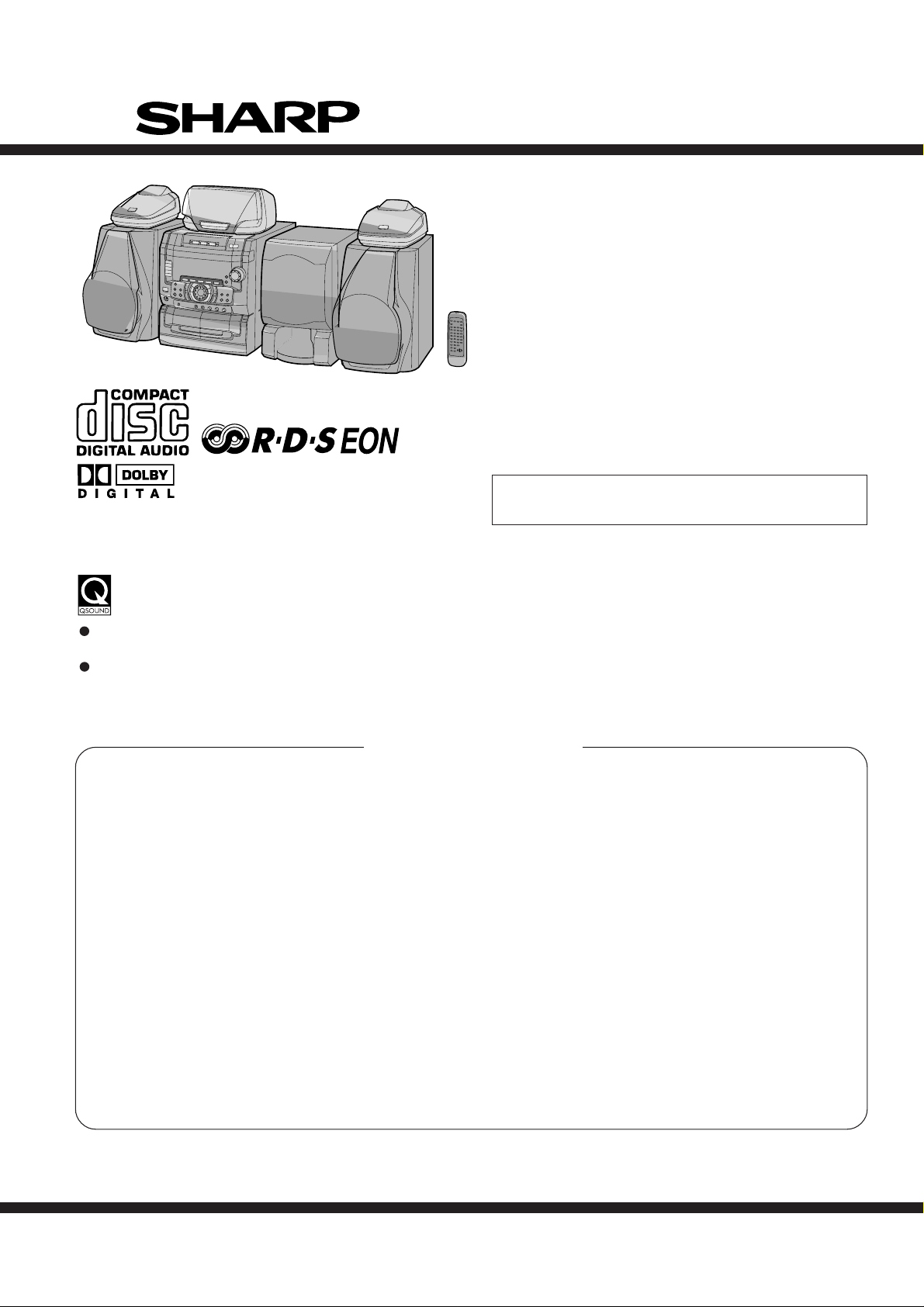
CD-K491W
No.S0883CDK491W/
CD-K491W
CD-K491W mini component system consisting of CD-K491W
mini component system, CP-K491, CP-SW491, centre
(GBOXS0010AWM3) and surround (GBOXS0011AWM3)
speaker system.
• In the interests of user-safety the set should be restored to its
original condition and only parts identical to those specified be
used.
QSOUND and the QLogo are registered trademarks of
QSound Labs, Inc.
QSound is protected under US Patent Nos. 5,105,462 and
5,208,860 and foreign counterparts.
CONTENTS
Page
SAFETY PRECAUTION FOR SERVICE MANUAL ........................................................................................................... 2
VOLTAGE SELECTION..................................................................................................................................................... 2
SPECIFICATIONS ............................................................................................................................................................. 3
NAMES OF PARTS ........................................................................................................................................................... 4
OPERATION MANUAL ...................................................................................................................................................... 7
DISASSEMBLY.................................................................................................................................................................. 8
REMOVING AND REINSTALLING THE MAIN PARTS................................................................................................... 11
ADJUSTMENT ................................................................................................................................................................. 12
NOTES ON SCHEMATIC DIAGRAM .............................................................................................................................. 16
TYPES OF TRANSISTOR AND LED................................................................................................................................16
BLOCK DIAGRAM ........................................................................................................................................................... 17
SCHEMATIC DIAGRAM / WIRING SIDE OF P.W.BOARD............................................................................................. 22
WAVEFORMS OF CD CIRCUIT...................................................................................................................................... 52
TROUBLESHOOTING ..................................................................................................................................................... 53
FUNCTION TABLE OF IC................................................................................................................................................ 57
FL DISPLAY..................................................................................................................................................................... 68
REPLACEMENT PARTS LIST/EXPLODED VIEW
SHARP CORPORATION
– 1 –
This document has been published to be used
for after sales service only.
The contents are subject to change without notice.
Page 2
CD-K491W
SAFETY PRECAUTION FOR SERVICE MANUAL
WARNINGS
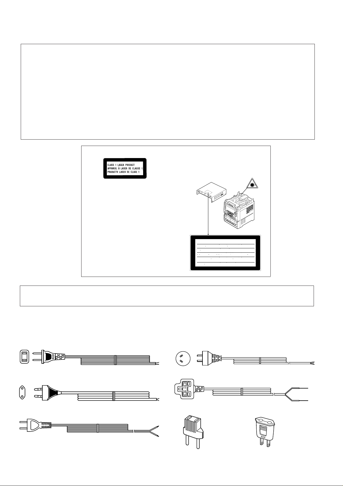
THE AEL (ACCESSIBLE EMISSION LEVEL) OF THE LASER POWER OUTPUT IS LESS THAN CLASS 1 BUT THE LASER
COMPONENT IS CAPABLE OF EMITTING RADIATION EXCEEDING THE LIMIT FOR CLASS 1. THEREFORE IT IS
IMPORTANT THAT THE FOLLOWING PRECAUTIONS ARE OBSERVED DURING SERVICING TO PROTECT YOUR EYES
AGAINST EXPOSURE TO THE LASER BEAM.
1-WHEN THE CABINET IS REMOVED, THE POWER IS TURNED ON WITDOUT A COMPACT DISC IN POSITION AND THE
PICK-UP IS ON THE OUTER EDGE THE LASER WILL LIGHT FOR SEVERAL SECONDS TO DETECT A DISC. DO NOT
LOOK INTO THE PICK-UP LENS.
2-THE LASER POWER OUTPUT OF THE PICK-UP UNIT AND REPLACEMENT SERVICE PARTS ARE ALL FACTORY
PRE-SET BEFORE SHIPMENT.
DO NOT ATTEMPT TO RE-ADJUST THE LASER PICK-UP UNIT DURING REPLACEMENT OR SERVICING.
3-UNDER NO CIRCUMSTANCES STARE INTO THE PICK-UP LENS AT ANY TIME.
4-CAUTION-USE OF CONTROLS OR ADJUSTMENTS, OR PERFORMANCE OF PROCEDURES OTHER THAN THOSE
SPECIFIED HEREIN MAY RESULT IN HAZARDOUS RADIATION EXPOSURE.
CAUTION
● This Mini Component System is classified as a
CLASS 1 LASER product.
● The CLASS 1 LASER PRODUCT label is located on
the rear cover.
● Use of controls, adjustments or performance of procedures other than those specified herein may result
in hazardous radiation exposure.
As the laser beam used in this compact disc player
is harmful to the eyes, do not attempt to disassemble
the cabinet. Refer servicing to qualified personnel
only.
Laser Diode Properties
Material: GaAIAs
Wavelength: 780 nm
Emission Duration: continuous
Laser Output: max. 0.6 mW
CAUTION-INVISIBLE LASER RADIATION WHEN OPEN. DO NOT STARE INTO
BEAM OR VIEW DIRECTLY WITH OPTICAL INSTRUMENTS.
VARNING-OSYNLIG LASERSTRALNING NAR DENNA DEL AR OPPNAD. STIRRA
EJ IN I STRALEN OCH BETRAKTA EJ STRALEN MED OPTISKA INSTRUMENT.
ADVERSEL-USYNLIG LASERSTRALING VED ABNING. SE IKKE IND I
STRALEN-HELLER IKKE MED OPTISKE INSTRUMENTER.
VARO! AVATTAESSA OLET ALTTIINA NAKYMATON LASERSATEILYLLE.
ALA TUIJOTA SATEESEEN ALAKA KATSO SITA OPTISEN LAITTEEN LAPI.
VARNING-OSYNLIG LASERSTRALNING NAR DENNA DEL AR OPPNAD.
STIRRA EJ IN I STRALEN OCH BETRAKTA EJ STRALEN GENOM OPTISKT
INSTRUMENT.
ADVERSEL-USYNLIG LASERSTRALING NAR DEKSEL APNES. STIRR IKKE
INN I STRALEN ELLER SE DIREKTE MED OPTISKE INSTRUMENTER.
VARO ! Avattaessa ja suojalukitus ohitettaessa olet alttiina näkymättömälle lasersäteilylle. Älä katso säteeseen.
VARNING! Osynlig laserstralning när denna del är öppnad och spärren är urkopplad. Betrakta ej strälen.
VOLTAGE SELECTION
The voltage selector is located on the AC voltage selector box. If adjustment is necessary, use a screwdriver in order to turn the
selector in either direction until the correct voltage figure is displayed in the window next to the adjustment screw.
QACCA0001AW00
QACCE0008AW00
QACCJ0003AW00
QACCL0005AW00
QACCB0006AW00
92LPLUG027
Figure 2 AC POWER SUPPLY CORD AND AC PLUG ADAPTOR
– 2 –
92LPLUG155A
Page 3

FOR A COMPLETE DESCRIPTION OF THE OPERATION OF THIS UNIT, PLEASE REFER
TO THE OPERATION MANUAL.
CD-K491W
CD-K491W
SPECIFICATIONS
● General
Power source: AC 110/127/220/230 - 240 V,
50/60 Hz
Power consumption: 200 W
Dimensions: Width; 270 mm (10-5/8")
Height; 316 mm (12-1/2")
Depth; 343 mm (13-1/2")
Weight: 10.5 kg (23.2 lbs.)
● Amplifier section
Output power: PMPO; 2,000 W (total)
Front speakers;
MPO; 142 W (71 W + 71 W)
(10 % T.H.D.)
RMS: 80 W (40 W + 40 W)
(10 % T.H.D.)
Centre speaker;
MPO; 71 W
(10 % T.H.D.)
RMS: 40 W
(10 % T.H.D.)
Surround speakers;
MPO; 142 W (71 W + 71 W)
(10 % T.H.D.)
RMS: 80 W (40 W + 40 W)
(10 % T.H.D.)
Sub woofer;
MPO; 71 W
(10 % T.H.D.)
RMS: 40 W
(10 % T.H.D.)
Output terminals: Front speakers; 8 ohms
Centre speaker; 8 ohms
Surround speakers; 8 ohms
Sub woofer; 8 ohms
Monitor; 1 Vp-p/75 ohms
Headphones; 16 - 50 ohms
(recommended; 32 ohms)
Input terminals: DVD 1 (Digital); Optical
DVD 2 (Digital); Coaxial
VCR 1/AUX 1; 500 mV/47 kohms
VCR 2/AUX 2; 500 mV/47 kohms
DVD 1/VCR 1; 1 Vp-p/75 ohms
DVD 2/VCR 2; 1 Vp-p/75 ohms
Microphone 1/2; 1 mV/4.7 kohms
● Tuner section
Frequency range: FM; 88 - 108 MHz
SW2; 9.5 - 21.85 MHz
SW1; 3.2 - 7.3 MHz
MW; 531 - 1,602 kHz
● Cassette deck section
Frequency response: 50 - 14,000 Hz (Normal tape)
Signal/noise ratio: 55 dB (TAPE 1, playback)
50 dB (TAPE 2, recording/
playback)
Wow and flutter: 0.15 % (WRMS)
● Compact disc player section
Type: 3-disc multi-play compact disc
player
Signal readout: Non-contact, 3-beam semi-
conductor laser pickup
D/A converter: 1-bit D/A converter
Frequency response: 20 - 20,000 Hz
Dynamic range: 100 dB (1 kHz)
CP-K491
● Front speaker section
Type: 3-way, 130 mm (5-1/8") woofer,
50 mm (2") tweeter and super
tweeter
Maximum input power: 80 W
Rated input power: 40 W
Impedance: 8 ohms
Dimensions: Width; 220 mm (8-11/16")
Height; 316 mm (12-1/2")
Depth; 284 mm (11-3/16")
Weight: 3.4 kg (7.5 lbs.)/each
GBOXS0010AWM3
● Centre speaker section
Type: 2-way, 120 mm (4-3/4") woofer
and 50 mm (2") tweeter
Maximum input power: 80 W
Rated input power: 40 W
Impedance: 8 ohms
Dimensions: Width; 270 mm (10-5/8")
Height; 142 mm (5-5/8")
Depth; 220 mm (8-11/16")
Weight: 1.8 kg (4.0 lbs.)
GBOXS0011AWM3
● Surround speaker section
Type: 2-way, 100 mm (4") woofer and
50 mm (2") tweeter
Maximum input power: 80 W
Rated input power: 40 W
Impedance: 8 ohms
Dimensions: Width; 200 mm (7-7/8")
Height; 134 mm (5-5/16")
Depth; 240 mm (9-1/2")
Weight: 1.4 kg (3.1 lbs.)/each
CP-SW491
● Sub woofer section
Type: 160 mm (6-1/2") woofer
Maximum input power: 80 W
Rated input power: 40 W
Impedance: 8 ohms
Dimensions: Width; 220 mm (8-11/16")
Height; 316 mm (12-1/2")
Depth; 294 mm (11-5/8")
Weight: 3.8 kg (8.4 lbs.)
Specifications for this model are subject to change without
prior notice.
– 3 –
Page 4
CD-K491W
CD-K491W
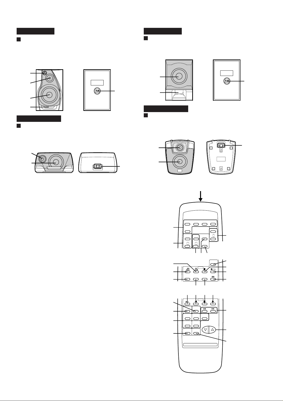
NAMES OF PARTS
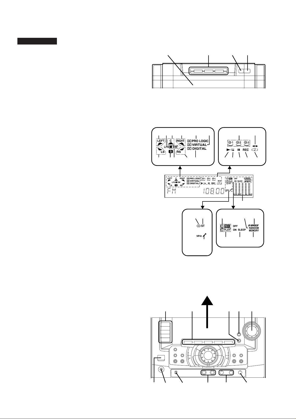
■ Front panel
1. Disc Tray
2. Disc Number Selector Buttons
3. Disc Skip Button
4. Open/Close Button
5. Left Front Speaker Indicator
6. LFE Indicator
7. Centre Speaker Indicator
8. Right Front Speaker Indicator
9. Dolby Pro Logic Indicator
10. Dolby Virtual Indicator
11. Left Surround Speaker Indicator
12. Surround Signal Indicator
13. Sub Woofer Indicator
14. Right Surround Speaker Indicator
15. Dolby Digital Indicator
16. (CD) Disc Number Indicator
17. (TAPE) Direction Indicator
18. (CD) Play Indicator
19. (CD) Repeat Play Indicator
20. (CD) Pause Indicator
21. (TAPE) Record Indicator
22. (TAPE) Reverse Mode Indicator
23. Spectrum Analyzer Indicator
24. (TUNER) FM Stereo Indicator
25. (TUNER) FM Stereo Mode Indicator
26. Karaoke Maker Indicator
27. Timer Record Indicator
28. (CD) Random Play Indicator
29. Extra Bass Indicator
30. Timer Play Indicator
31. Sleep Indicator
32. (CD/TUNER) Memory Indicator
1
6
5
1213 14
11
89
7
234
16
30
15
24
25
26
10
18 192021 22
27
23
31
28
17
29
32
33. Function Selector Buttons
34. Surround Mode Selector Buttons
35. Equalizer Selector/Demo Mode Button
36. Extra Bass Button
37. Volume Control
38. On/Stand-by Button
39. Headphone Socket
40. Karaoke Maker Switch
41. Microphone Sockets
42. Microphone Level Controls
43. Digital Echo Control
– 4 –
33
39 41 43
38
34 35
40
42
36 37
Page 5
62 63
VIDEO OUT
MONITOR
SPAN
SELECTOR
FM/MW(kHZ)
50/9
100/10
1
234
5
67
8
10
11
13
15 16
17 18
9
12
14
44 45
46 47 48 49 50 51
52
53 54 55
56
57 58 59 60
61
44. Clock Button
45. Sleep Button
46. Reverse Mode Button
47. CD Pause Button
48. Jog Dial
49. (CD/TAPE) Stop Button
50. Record Pause Button
51. Menu Button
52. Item Button
53. Timer Button
54. Memory Button
55. Clear Button
56. (CD) Track Down/Review Button
57. (TAPE 2) Reverse Play Button
58. (CD) Play/Repeat Button
59. (CD) Track Up/Cue Button
60. (TAPE) Normal Edit Button
61. (TAPE) High Edit/Beat Cancel Button
(TAPE 2) Fast Wind Button
(TUNER) Tuning Down Button
(TAPE 1) Play Button
(TAPE 2) Forward Play Button
(TAPE) Fast Wind Button
(TUNER) Tuning Up Button
CD-K491W
62. (TAPE 1) Cassette Compartment
63. (TAPE 2) Cassette Compartment
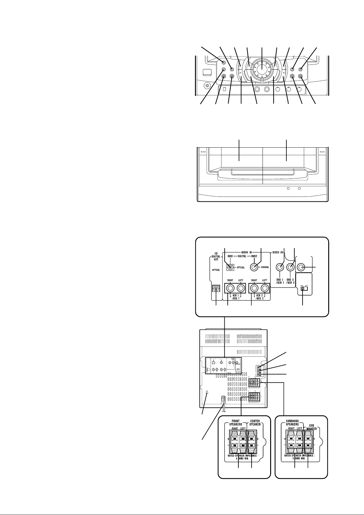
■ Rear panel
1. DVD 1 Digital Input Socket (Optical)
2. DVD 2 Digital Input Socket (Coaxial)
3. DVD 1/VCR 1 Video Input Socket
4. DVD 2/VCR 2 Video Input Socket
5. Video Output Socket
6. CD Digital Output Socket (Optical)
7. VCR 1/AUX 1 Input Socket
8. VCR 2/AUX 2 Input Socket
9. Span Selector Switch
10. 75 Ohm FM Aerial Socket
11. Aerial Earth Terminal
12. SW1/SW2/MW Aerial Terminal
13. AC Voltage Selector
14. AC Power Lead
15. Front Speaker Terminals
16. Centre Speaker Terminals
17. Surround Speaker Terminals
18. Sub Woofer Terminals
– 5 –
Page 6
CD-K491W
CP-K491 CP-SW491
Front speakers
1. Super Tweeter
2. Tweeter
3. Woofer
4. Bass Reflex Duct
5. Speaker Terminals
Sub Woofer
1. Woofer
2. Bass Reflex Duct
3. Speaker Terminals
1
2
5
3
1
3
2
4
GBOXS0010AWM3
Centre speaker
1. Tweeter
2. Woofer
3. Speaker Terminals
1
2
■ Remote control
1. Remote Control Transmiter LED
2. Surround Mode Selector Buttons
3. Sub Woofer Level Control Buttons
4. Setup Up/Down Buttons
5. Menu Button
6. Item Button
● Tuner control section
7. Preset Up/Down Buttons
● CD control section
8. Track Up/Cue Button
9. Track Down/Review Button
10. Memory Button
11. Disc Skip Button
12. Stop Button
13. Play/Repeat Button
14. Pause Button
15. Clear Button
16. Random Button
GBOXS0011AWM3
Surround speakers
1. Tweeter
2. Woofer
3. Speaker Terminals
1
3
2
3
1
2
7
3
5
6
10
4
8
9
15 16
17
18 19 20
11
12
13
14
● Tape control section
17. (TAPE 2) Record Pause Button
18. (TAPE 2) Reverse Play Button
19. Stop Button
20. (TAPE 1) Play Button
(TAPE 2) Forward Play Button
21. (TAPE 2) Fast Wind Buttons
● Common section
22. Extra Bass Button
23. Equalizer Mode Button
24. Function Selector Buttons
25. On/Stand-by Button
26. Volume Control Buttons
27. Dimmer Button
– 6 –
22
23
24
25
21
26
27
Page 7
OPERATION MANUAL
SETTING THE CLOCK
1
Press the ON/STAND-BY button to enter the stand-by mode.
2
Press the CLOCK button.
3
Within 5 seconds, press the MEMORY button.
4
Turn the jog dial to select the time display mode.
"0:00" → The 24-hour display will appear.
(0:00 - 23:59)
"AM 12:00" → The 12-hour display will appear.
(AM or PM 12:00 - 11:59)
"AM 0:00" → The 12-hour display will appear.
(AM or PM 0:00 - 11:59)
● Note that this can only be set when the unit is first installed
or it has been reset (see page 42).
5
Press the MEMORY button.
6
Adjust the hour by turning the jog dial.
● When the jog dial is turned one click clockwise, the time will
increase by 1 hour. When it is turned one click anticlockwise,
the time will decrease by 1 hour.
Keep turning the jog dial to change the time continuously.
● When the 12-hour display is selected, "AM" will change auto-
matically to "PM".
7
Press the MEMORY button.
8
Adjust the minutes by turning the jog dial.
● When the jog dial is turned one click clockwise, the time will
increase by 1 minute. When it is turned one click anticlockwise,
the time will decrease by 1 minute.
Keep turning the jog dial to change the time continuously.
● The hour setting will not advance even if minutes advance from
"59" to "00".
9
Press the MEMORY button.
● The clock starts operating from "0" seconds.
(Seconds are not displayed.)
Note:
● In the event of a power failure or when the AC power lead is
disconnected, the clock display will go out.
When the AC power supply is restored, the clock display will
flash on and off to indicate the time when the power failure
occurred or when the AC power lead was disconnected.
If this happens, follow the procedure below to change the clock
time.
To change the clock time:
When the unit is in the stand-by mode:
➀ Press the MEMORY button.
➁ Perform steps 6 - 9 above.
When the unit is on:
➀ Press the CLOCK button.
➁ Within 5 seconds, press the MEMORY button.
➂ Perform steps 6 - 9 above.
To see the time display:
Press the CLOCK button.
● The time display will appear for about 5 seconds.
To change the time display mode:
➀ Perform steps 1 and 2 in the section "RESETTING THE MI-
CROCOMPUTER", on page 42.
➁ Perform steps 1 - 9 above.
CLOCK
ON/
STAND-BY
MEMORY
TUNING
( )
Jog dial
In this example, the clock is set for the
12-hour (AM 12:00) system.
0:00 AM 12:00 AM 0:00
2
3
4
5
6
7
8
9
SPAN
SELECTOR
FM/MW(kHz)
50/9
100/10
(Continued)
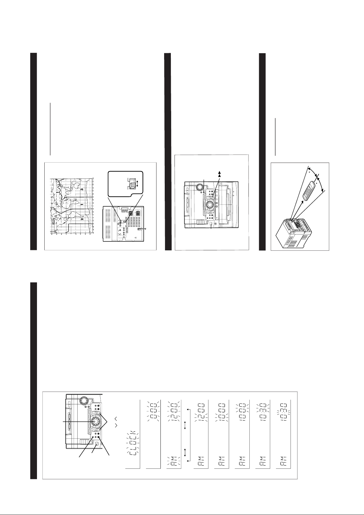
■FM/MW interval (span)
The International Telecommunication Union (ITU) has established
that member countries should maintain either a 10 kHz or a 9
kHz interval between broadcasting frequencies of any MW sta-
tion. The illustration shows the 9 kHz interval zones (regions 1
and 3), and the 10 kHz interval zone (region 2).
Before using the unit, set the SPAN SELECTOR switch (on the
rear panel) to MW tuning interval (span) of your area.
To change the tuning zone:
1 Press the ON/STAND-BY button to enter the stand-by mode.
2 Set the SPAN SELECTOR switch to "50/9" for 9 kHz MW
interval (50 kHz FM interval), and "100/10" for 10 kHz MW
interval (100 kHz FM interval).
3 Press the ON/STAND-BY button whilst holding down the
button and the EQUALIZER/DEMO button.
Caution:
● The operation explained above will erase all data stored in
memory including clock and timer settings, and tuner and CD
presets.
RESETTING THE MICROCOMPUTER
ON/
STAND-BY
EQUALIZER
/DEMO
Reset the microcomputer by performing the following
procedure for the cases shown below:
● To erase all of the stored memory contents, or
● If the display does not function properly, or
● The unit does not operate properly.
1
Press the ON/STAND-BY button to enter the stand-by
mode.
2
Press the ON/STAND-BY button whilst holding down the
button and the EQUALIZER/DEMO button.
Caution:
● The operation explained above will erase all data stored
in memory including clock and timer settings, and tuner
and CD presets.
(Continued)
■Remote control
● When inserting or removing the batteries, push them towards
the battery terminal.
● Installing the batteries incorrectly may cause the unit to mal-
function.
Notes concerning use:
● Replace the batteries if control distance decreases or operation
becomes erratic.
● Periodically clean the transmitter LED on the remote control
and the sensor on the main unit with a soft cloth.
● Exposing the sensor on the main unit to strong light may in-
terfere with operation. Change the lighting or the direction of
the unit.
● Keep the remote control away from moisture, excessive heat,
shock, and vibrations.
15
15
0.2 m - 6 m
(8" - 20')
CD-K491W
– 7 –
Page 8
CD-K491W
DISASSEMBLY
Caution on Disassembly
Follow the below-mentioned notes when disassembling
the unit and reassembling it, to keep it safe and ensure
excellent performance:
1. Take cassette tape and compact disc out of the unit.
2. Be sure to remove the power supply plug from the wall
outlet before starting to disassemble the unit.
3. Take off nylon bands or wire holders where they need to
be removed when disassembling the unit. After servicing
the unit, be sure to rearrange the leads where they were
before disassembling.
4. Take suffcient care on static electricity of integrated
circuits and other circuits when servicing.
CD-K491W
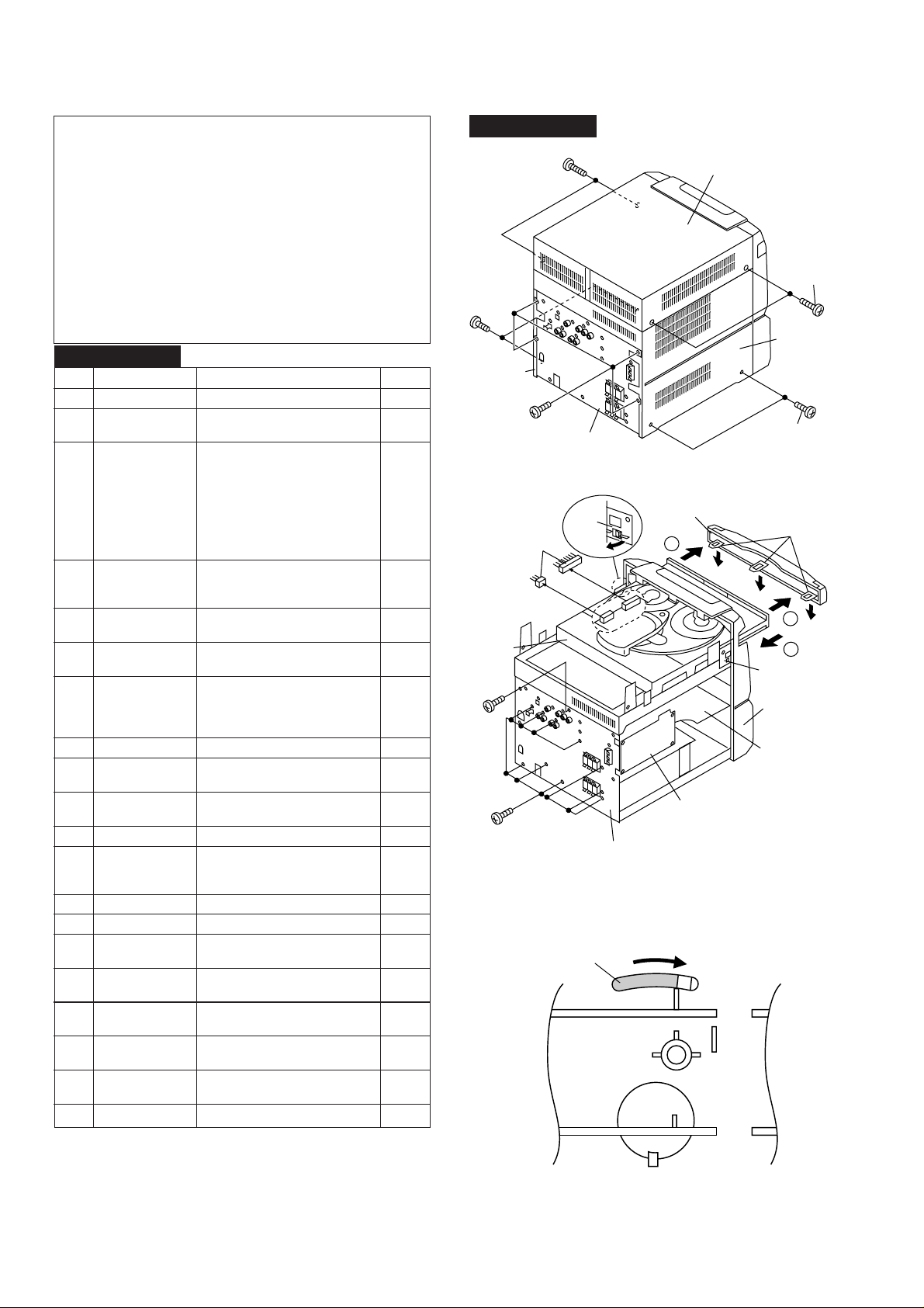
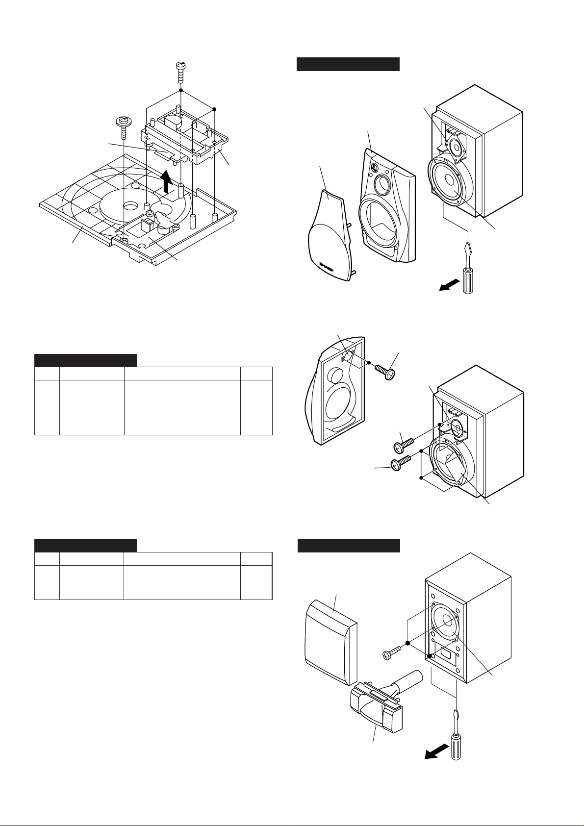
STEP REMOVAL
1 Top Cabinet 1. Screw ..................... (A1) x4 8-1
2 Side Panel 1. Screw ..................... (B1) x8 8-1
(Left/right)
3 CD Player Unit/ 1. Turn on the power supply, 8-2
CD Tray Cover open the disc tray, take out
4 Dolby PWB 1. Flat cable ............... (D1) x2 9-1
5 Tuner PWB 1. Socket.................... (E1) x1 9-1
6 Rear Panel 1. Screw ..................... (F1) x11 8-2
7 Main PWB 1. Flat cable ............... (G1) x2 9-1
8 Karaoke PWB 1.Screw ...................... (H1) x3 9-2
9 Front Panel 1. Flat wire ................. (J1) x1 9-2
10
Power Amp. PWB
with Heat Sink 2. Screw ..................... (K2) x6
11
Power Supply PWB
12 Display PWB 1. Knob ....................... (M1) x2 9-4
13 CD Switch PWB 1. Screw..................... (N1) x3 9-4
14 Headphones 1. Screw ..................... (P1) x1 9-4
15 Tape Mechanism 1. Open the cassette Lid.
16 Turntable 1. Screw ..................... (R1) x1 9-5
17 Disc Tlay 1. Screw ..................... (S1) x2 9-5
18 CD Servo PWB 1. Screw ..................... (T1) x1 9-6
19 CD Changer 1. Screw ..................... (U1) x4 10-1
Mechanism
20 CD Mechanism 1. Screw ..................... (V1) x1 10-1
the CD cover, and close.
(Note 1)
2. Hook....................... (C1) x3
3. Hook....................... (C2) x2
4. Screw ..................... (C3) x1
5. Socket .................... (C4) x3 8-2,9-1
2. Socket .................... (D2) x1
3. Screw ..................... (D3) x12
2. Screw ..................... (E2) x5
2. Flat wire .................
3. Socket...................... (G3) x5
4. Screw....................... (G4) x3
2. Screw...................... (J2) x2
1. Socket .................... (K1) x3 9-2
1. Screw ..................... (L1) x6 9-3
2. Nut.......................... (M2) x1
3. Screw ..................... (M3) x12
2. Screw ..................... (Q1) x6 9-4
2. Cover ..................... (R2) x1
2. Guide ..................... (S2) x2
2. Socket .................... (T2) x4
PROCEDURE
................................... 9-1
(G2) x3
FIGURE
( B1 ) x2
ø3 x8mm
Side Panel
(Right)
( B1 ) x4
ø3 x8mm
CD Player
Unit
( C3 ) x1
ø3 x8mm
CD-K491W
( A1 ) x2
ø3 x12mm
Rear Panel
( C4 ) x2
( F1 ) x10
ø3 x8mm
LOCK
LEVER
(C2) x1
Pull
Figure 8-1
CD Tray Cover
Rear Panel
Figure 8-2
Top Cabinet
( A1 ) x2
ø3 x12mm
Side Panel
(Left)
( B1 ) x2
ø3 x8mm
Hook
( C1) x3
1
1
2
( C2 ) x1
Front Panel
Main PWB
Tuner PWB
Note 1:
How to open the changer manually. (Fig. 8-3)
1. Then, turn fully the lock lever in the arrow direction through
the hole on the loading chassis bottom in this state.
After that, push forward the CD player base.
Figure 8-3
– 8 –
Page 9
CD-K491W
(D1) x1
(F1) x1
ø3 x10mm
(C4) x1
(D2) x1
(D3) x8
ø3x10mm
(E2) x1
ø3x10mm
(D3) x4
ø3x10mm
Rear Panel
(H1)x2
ø3x10mm
Karaoke
PWB
Dolby PWB
(D1) x1
(G3)
(G3) x1
(G2) x1
@
x2
(G1) x2
(G2) x2
(E1) x1
Tuner PWB
Figure 9-1
(G4) x2
ø3x10mm
Front Panel
(E2) x4
ø3 x10mm
Front Panel
(G3) x2
Main PWB
(G4) x1
ø3x10mm
Front Panel
(N1)x3
ø3x10mm
(M3)x12
ø3x10mm
Tape Mechanism
CD Switch PWB
(Q1)x6
ø3x10mm
Figure 9-4
( R1 ) x1
ø3 x10mm
( R2 ) x1
(M1)x2
Washer
(M2)x1
Display
PWB
Headphones
PWB
Open
(P1)x1
ø3x10mm
Cassette
Holder (Left/Right)
(H1)x1
ø3x10mm
(K2)x5
ø3x10mm
(L1)x4
ø4x8mm
Power Supply PWB
( K1 ) x1
Power Amp. PWB
Figure 9-2
( K2 ) x1
ø3x10mm
(L1)x1
ø3x10mm
(K1 ) x2
(J1 ) x1
( J2 ) x2
ø3x10mm
( S1 ) x1
ø3 x10mm
( S2 ) x1
( T2 ) x2
CD Player Unit
Turntable
Disc Tray
( S1 ) x1
ø3 x10mm
( S2 ) x1
Figure 9-5
( T1 ) x1
ø3 x10mm
CD Servo PWB
(L1)x1
ø3x10mm
Figure 9-3
( T2 ) x2
CD Player Unit
Figure 9-6
– 9 –
Page 10
CD-K491W
( U1 ) x4
ø3 x12mm
( V1 ) x1
ø2.6 x10mm
Shift Lever
CD Changer
Mechanism
CD Player Base
CD Mechanism
Be careful when installing the CD changer mechanism.
Install the CD changer mechanism on the CD player base after
the shift lever has been set in the highest position.
Figure 10-1
CP-K491
STEP REMOVAL
1 Front Speaker 1. Net.......................... (A1) x1 10-2
2. Baffle Board ........... (A2) x1
3. Screw ..................... (A3) x2
4. Screw ..................... (A4) x4
5. Screw ..................... (A5) x2
PROCEDURE
FIGURE
CP-K491
Tweeter
Baffle Board
(A2)x1
Net
(A1)x1
Woofer
Screw driver
Super
Tweeter
(A5)x2
ø3x10mm
Tweeter
(A3)x2
ø3x10mm
CP-SW491
STEP REMOVAL PROCEDURE FIGURE
1 Sub woofer 1. Net.......................... (A1) x1 10-3
2. Duct Panel ............. (A2) x1
3. Screw ..................... (A3) x4
Note:
The center and rear speakers can be easily disassembled.
Therefore the disassembling method is not discribed.
For details refer to the disassembling drawing in the Parts
Guide.
(A4)x4
ø4x16mm
Woofer
Figure 10-2
CP-SW491
Net
( A1 ) x1
( A3 ) x4
ø4 x16mm
Woofer
– 10 –
( A2 ) x1
Screwdriver
Figure 10-3
Page 11
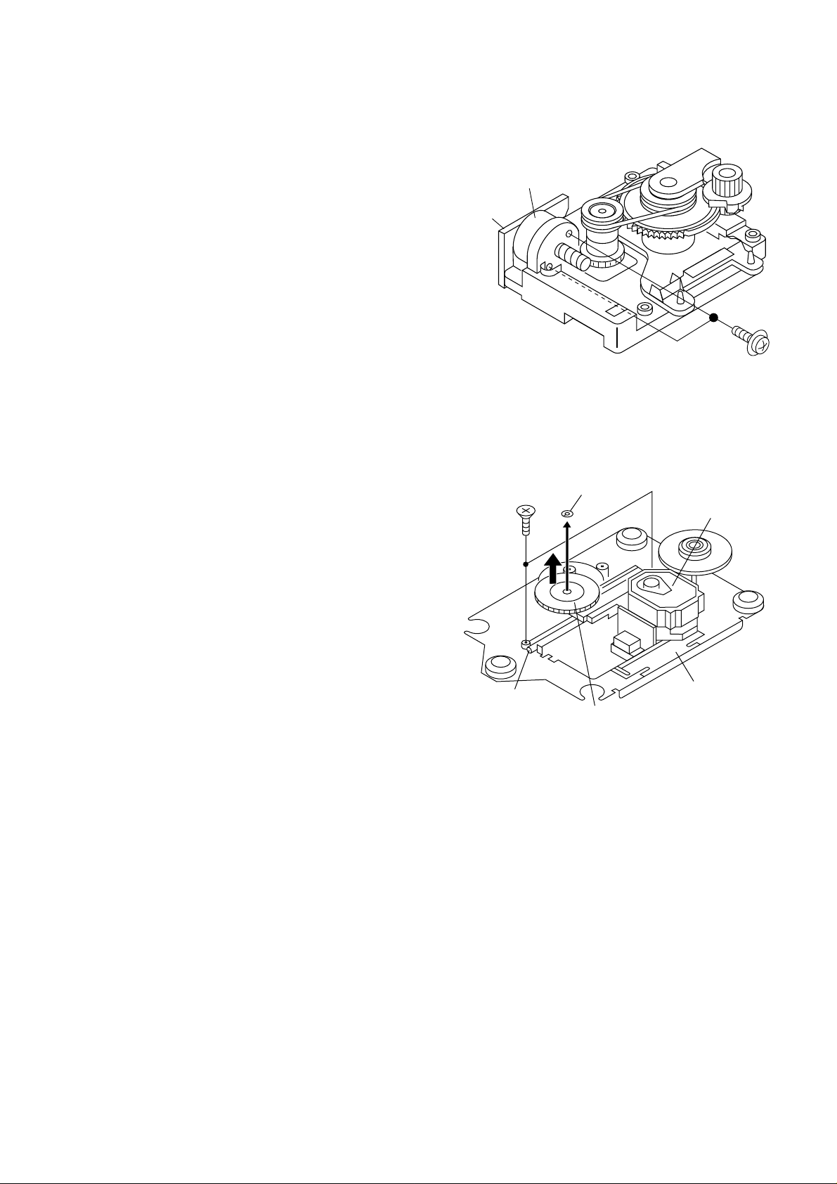
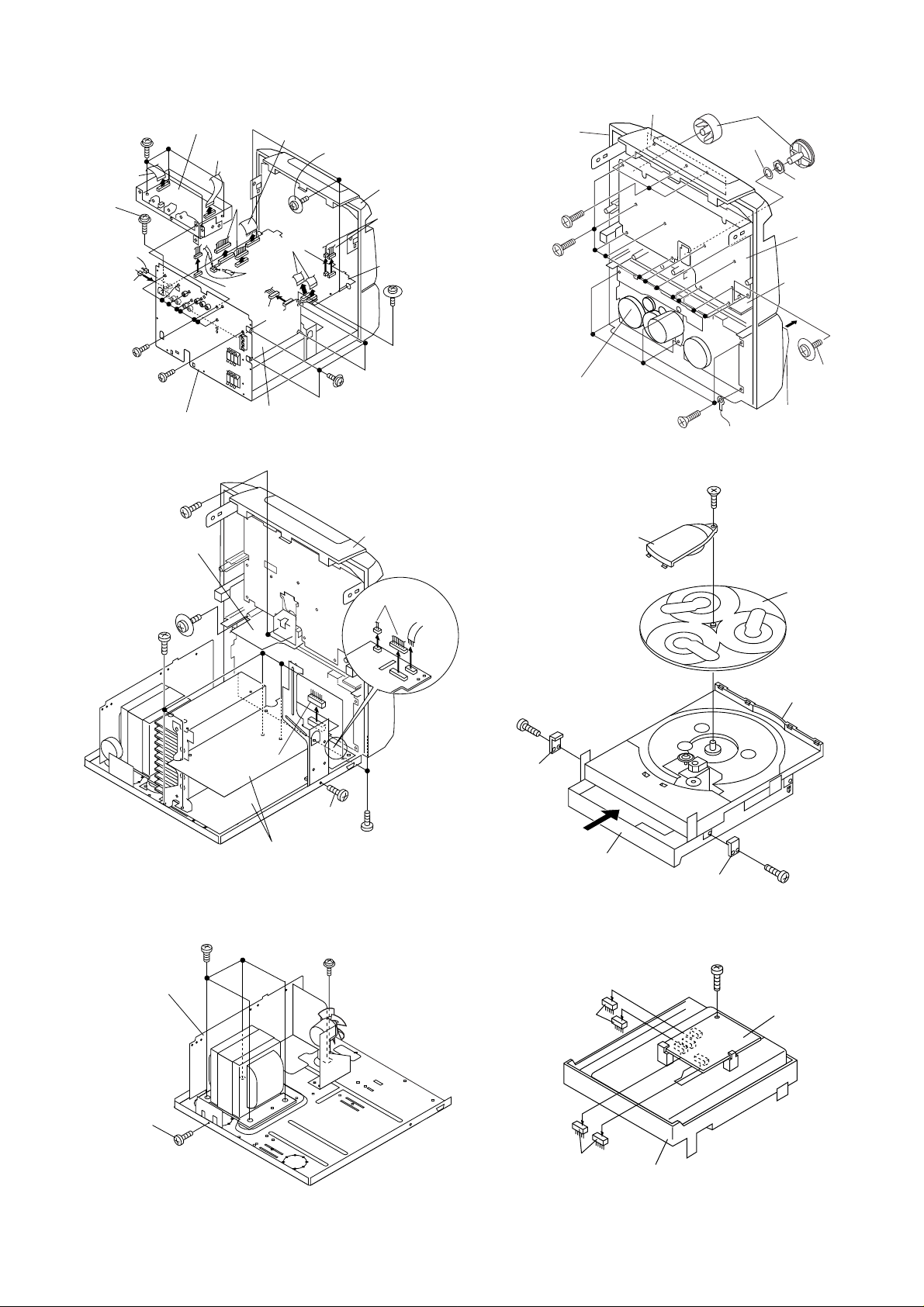
REMOVING AND REINSTALLING THE MAIN PARTS
( A1 ) x2
ø2.6 x5mm
Loading/Up/
Down Motor
Motor
PWB
CD MECHANISM SECTION
Perform steps 1, 2, 3,16, 17, 18, 19 and 20 of the disassembly
method to remove the CD mechanism.
How to remove the loading motor
(See Fig. 11-1)
1. Remove the screws (A1) x 2 pcs., to remove the loading
motor.
How to remove the pickup (See Fig. 11-2)
1. Remove the screws (B1) x 2 pcs., to remove the shaft (B2).
2. Remove the stop washer (B3) x 1 pc., to remove the gear
(B4).
3. Remove the pickup.
( B1 ) x2
ø2.6 x6mm
CD-K491W
Figure 11-1
Stop Washer
( B3 ) x1
Pickup
Shaft
( B2 ) x1
CD Mechanism
Gear
( B4 ) x1
Figure 11-2
– 11 –
Page 12
CD-K491W
ADJUSTMENT
MECHANISM SECTION
• Driving Force Check
Torque Meter
Play: TW-2412 Tape 1: Over 80 g
• Torque Check
Torque Meter
Tape 1
Play: TW-2111 30 to 60 g. cm 30 to 100 g.cm
Fast forward: TW-2231 — 50 to 100 g.cm
Rewind: TW-2231 — 50 to 100 g.cm
• Tape Speed
Test Tape
Normal MTT-111 VRM01 3,000 ± Speaker
speed 30 Hz terminal
Adjusting
Point
Specified Value
Tape 2: Over 80 g
Specified Value
Specified
Value
Tape 2
Instrument
Connection
(Load
resistance:
8 ohms)
TUNER SECTION
fL: Low-range frequency
fH: High-renge frequency
• AM IF/RF
Signal generator: 400 Hz, 30%, AM modulated
Test Stage
IF 450 kHz 1,602 kHz T351 *1
MW Band — 531 kHz (fL): T306 *2
Coverage 1.1 ± 0.1 V
SW1 Band — 3.2 MHz (fL): T307 *2
Coverage 2.0 ± 0.1V
SW1 Band — 7.3 MHz (fH): TC305 *2
Coverage 7.7 ± 0.2 V
SW2 Band — 9.5 MHz (fL): T308 *2
Coverage 2.1 ± 0.1V
SW2 Band — 21.85 MHz (fH): TC304 *2
Coverage 7.7 ± 0.2V
MW 990 kHz 990 kHz T302 *1
Tracking
SW1 3.9 MHz 3.9 MHz (fL): T303 *1
Tracking
SW1 7.1 MHz 7.1 MHz (fH): TC303 *1
Tracking
SW2 11.65 MHz 11.65 MHz (fL): T304 *1
Tracking
SW2 21.45 MHz 21.45 MHz (fH): TC302 *1
Tracking
Frequency
Frequency
Display
Setting/
Adjusting
Parts
Instrument
Connection
TAPE MECHANISM PWB
VRM01
TAPE
FAS
SW
Figure 12
SPEED
*1. Input: Antenna, Output: TP302
*2. Input: Anetnna, Output: TP301
– 12 –
Page 13
• FM RF
Signal generator: 1 kHz, 40 kHz dev, FM modulated
Test Stage
Band — 87.5 kHz (fL): LT02 *1
Coverage 3.7 ± 0.1 V
RF 98 MHz 98 MHz LT01 *2
*1. Input: Antenna, Output: TP301
*2. Input: Anetnna, Output: Speaker Terminal
Frequency
10 - 30 dB
Frequency
Display
Setting/
Adjusting
Parts
Instrument
Connection
• Setting the Test Mode
Keeping the PAUSE button and TUNER button pressed, turn
on POWER. Then, the frequency is initially set in the memory
as shown in Table. Call it with the PRESET button to use it for
adjustment and check of tuner circuit.
Preset
No.
21 ~ 40
FM Preset
1 87.50 MHz 6 531 kHz 11 3.2 MHz 16 9.5 MHz
2 108.00 MHz 7 1,602 kHz 12 7.3 MHz 17 21.85MHz
3 90.00 MHz 8 603 kHz 13 3.9 MHz 18 11.65 MHz
4 106.00 MHz 9 1,404 kHz 14 7.1 MHz 19 21.45 MHz
5 98.00 MHz 10 990 kHz 15 5.06 MHz 20 15.1 MHz
No.
MW
Preset
No.
SW1
Preset
No.
SW2
CD-K491W
• FM Detection
Signal generator: 10.7 MHz, FM sweep
Test Stage
IF 10.7 MHz 98 MHz TT01 *1
*1. Input: Antenna, Output: TP301
*2. Input: Anetnna, Output: Speaker Terminal
• FM Mute Level
Signal generator: 1kHz, 40 kHz dev., FM modulated
Frequency Adjusting
98.00 MHz 98.00 MHz VR351 *1 Input: Antenna
(25 dBµV) Output: Speaker
*1. Adjust so that an output signal appears.
Frequency
Frequency
Display
Frequency
Display
Setting/
Adjusting
Parts
(Turn the
core of transformer TT01
fully counterclock wise)
Parts
Instrument
Connection
Instrument
Connection
Terminal
R357
TUNER PWB
T351
AM IF
IC303
TP302
VR351
FM Mute
Level
fL fH
SW2
Coverage
SW1 Band
Coverage
fL fH
T307 TC305
T308 TC304
FM Band
Coverage
LT02
T306
MW Band
Coverage
FM IF FM RF
TT01
TP301
LT01
SW2 Tracking
fH fL
T304TC302
T303TC303
T302
MW
Tracking
SO301
ANTENNA
TERMINAL
fH fL
SW1
Tracking
Figure 13 ADJUSTMENT POINTS
– 13 –
Page 14
CD-K491W
TEST MODE
• Setting the test mode
Any one of test mode can be set by pressing several keys as follows.
<CD> + <EQ> + <POWER> TEST: CD operation test
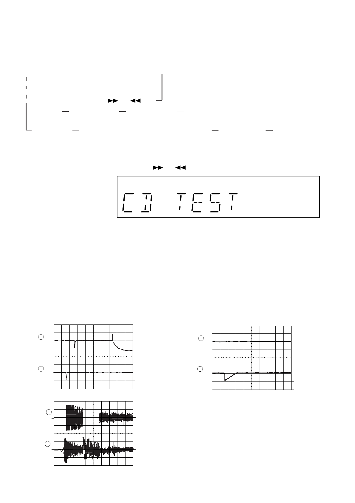
• TEST mode
Function — CD test mode
Setting of TEST mode
Indication of CD TST mode (Fig. 14-1)
OPEN/CLOSE operation is manual operation.
The pickup can be moved by using the (
<MEMORY>
LASER ON
<MEMORY>
Tracking on the spot.
SERVO OFF PLAY
) or ( ) key.
<MEMORY>
Tracking on the spot.
SERVO ON PLAY
IL is not performed.
<STOP>
STOP
<PLAY> key input
TOC. IL is performed, and the ordinary PLAY is performed.
If the following key is pressed during PLAY, it is possible
to specify directly any Track No.
<Disc Number 1> key: Track 4
<Disc Number 2> key: Track 9
Press <STOP> key.
Stop
<Disc Number 3> key: Track 15
Note:
Only in STOP state it is possible to slide the pickup with the ( ) or ( ) key.
VOL. --- Last memory
BAL. --- CENTER
R.GEQ. --- FLAT
X-BAS --- OFF
Canceling method - POWER OFF
Figure 14-1
CD SECTION
Since this CD system incorporates the following automatic adjustment function, when the pickup is replaced, it is not necessary
to readjust it.
Since this CD unit does not need adjustment, the combination of PWB and laser pickup unit is not restricted.
• Automatic adjustment item
1. Focus offset (Fig. 14-2)
2. Tracking offset (Fig. 14-3)
3. E/F balance (tracking error balance) (Fig. 14-4)
4. RF level AGC function (HF level: constant)
5. RF level automatic follow-up of the tracking gain
This automatic adjustment is performed each time a disc is changed. Therefore,
each disc is played back using the optimal settings.
0.1s
0.50 V
IC1 20 FE
0.1s
0.50 V
IC1 7 TE
FOCUS
OFF-SET
ADJUST
TRACKING
OFF-SET
ADJUST
1
2
10ms
0.50 V
IC1 20 FE
10ms
0.50 V
IC1 7 TE
Figure 14-2
200 ms
1V/diV
IC 1 15
200 ms
1V/diV
IC 1 7
TO
TE
TRACKING/
ERROR
BARANCE
1
ADJUST
2
Figure 14-4
– 14 –
Figure 14-3
Enlarged
View
TRACKING
OFF-SET
ADJUST
1
2
Page 15
DVD 1
/VCR 1
DVD 2
/VCR 2
DVD 1
/VCR 1
DVD 2
/VCR 2
When you connect this unit to a DVD player which is playing
a disc with the trademark, you can enjoy
realistic, powerful sound by playing back the recorded signal
through 6 speakers with the sound coming from the front
left, front right, centre, surround left, surround right and sub
woofer speakers.
To listen to a disc using the Dolby Digital mode:
1
Connect a DVD player. (See page 39.)
2
Press the DVD 1/VCR 1 or DVD 2/VCR 2 button to select
"DVD 1" or "DVD 2".
3
Start the DVD player.
Note:
● When the Dolby Digital surround mode is being used, the
equalizer will be set to FLAT.
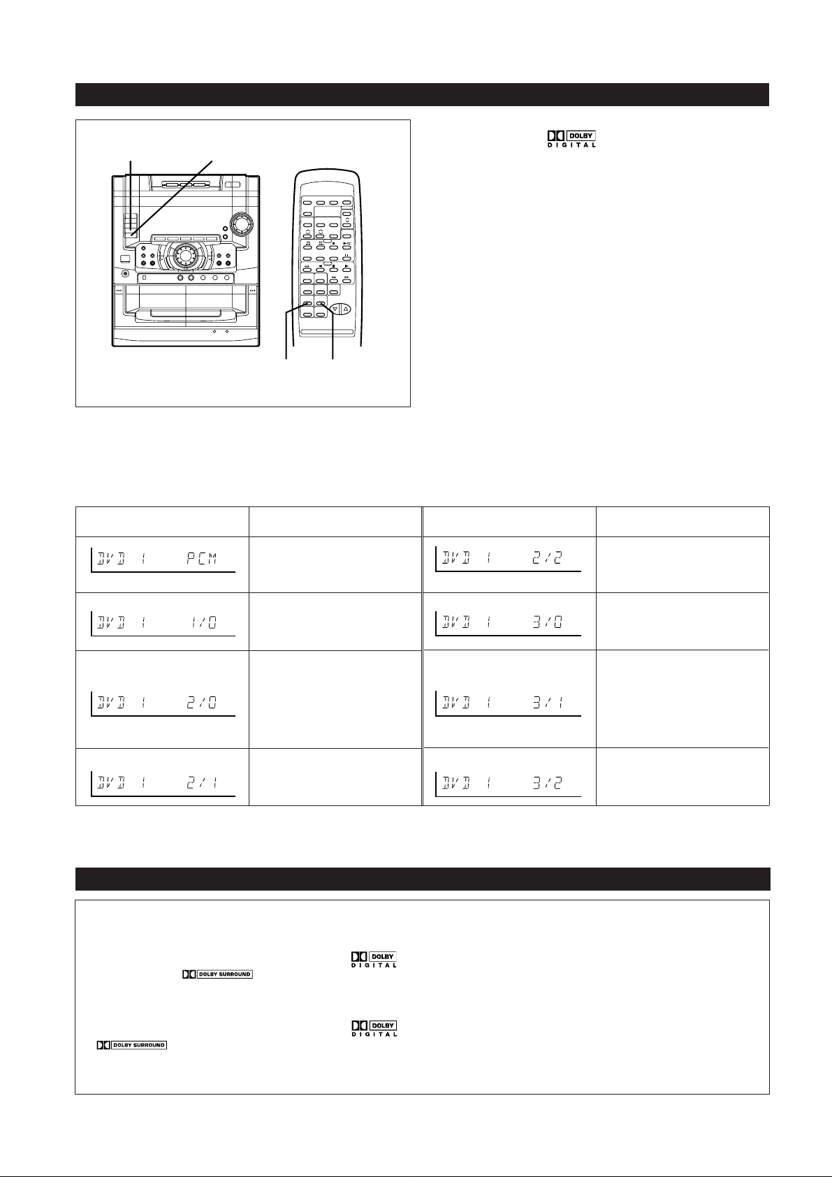
Type of Dolby digital signal
There are different types of Dolby digital signals. The type of Dolby digital signal being input into this unit can be checked
in the display.
Display Channels available Display Channels available
Normal PCM playback Front (L, R) + surround
(L, R)
Centre only (monaural) Front (L, R) + centre
Front (L, R)
(When the surround mode
is set to Normal or
Phantom, sound will also be
heard from the surround
speakers.)
Front (L, R) + centre +
surround (monaural)
Front (L, R) + surround
(monaural)
Front (L, R) + centre +
surround (L, R)
● If a low frequency sound effect (Low Frequency Effect) contains a Dolby digital signal, "LFE" will light in the display.
When this "LFE" is lit, low frequency signals will be output from the sub woofer.
DOLBY DIGITAL
SURROUND EFFECT CONTROL
This product allows you to enjoy 4 surround modes.
Normal mode:
When you play a sound source that has the
(5.1 channels) or trademarks, you can enjoy
surround sound using all 6 speakers.
Phantom mode:
When you play a sound source that has the
or trademarks, you can enjoy surround sound
using 5 speakers, but not the centre speaker.
Virtual Dolby Surround:
You can enjoy a three-dimensional surround stereo image
using just the 2 front speakers.
Enhanced Virtual Surround:
You can enjoy surround sound, using only the 2 front
speakers, but this mode increases the three-dimensional
stereo image effect even more.
CD-K491W
– 15 –
Page 16
CD-K491W
NOTES ON SCHEMATIC DIAGRAM
• Resistor:
To differentiate the units of resistors, such symbol as K and
M are used: the symbol K means 1000 ohm and the symbol
M means 1000 kohm and the resistor without any symbol is
ohm-type resistor. Besides, the one with “Fusible” is a fuse
type.
• Capacitor:
To indicate the unit of capacitor, a symbol P is used: this
symbol P means micro-micro-farad and the unit of the
capacitor without such a symbol is microfarad. As to
electrolytic capacitor, the expression “capacitance/withstand
voltage” is used.
(CH), (TH), (RH), (UJ): Temperature compensation
(ML): Mylar type
(P.P.): Polypropylene type
• Schematic diagram and Wiring Side of P.W.Board for this
model are subject to change for improvement without prior
notice.
REF. NO DESCRIPTION POSITION POSITIONREF. NO DESCRIPTION
SW1 OPEN/CLOSE ON—OFF
SW2 MECHA UP ON—OFF
SW3 DISC NUMBER ON—OFF
SW4 PICKUP IN ON—OFF
SW991 VOLTAGE SELECTOR 230-240V
SWD01 VOLUME JOG ON—OFF
SWD02 JOG ON—OFF
SWD03 X-BASS ON—OFF
SWD04 PRE EQ. ON—OFF
SWD05 MENU ON—OFF
SWD06 ITEM ON—OFF
SWD12 TUNING UP/CUE ON—OFF
SWD13 STOP ON—OFF
SWD14 NORMAL EDIT ON—OFF
SWD15 HIGH EDIT ON—OFF
SWD16 REC/PAUSE ON—OFF
SWD17 F-PLAY ON—OFF
SWD23 QSOUND ON—OFF
SWD26 VIRTUAL ON—OFF
SWD27 PHANTOM ON—OFF
SWD28 NORMAL ON—OFF
SWD29 BYPASS ON—OFF
SWD30 TUNING DOWN/REWIND ON—OFF
SWD31 CD PAUSE ON—OFF
• The indicated voltage in each section is the one measured
by Digital Multimeter between such a section and the chassis with no signal given.
1. In the tuner section,
( ) indicates AM
< > indicates FM stereo
2. In the main section, a tape is being played back.
3. In the deck section, a tape is being played back.
( ) indicates the record state.
4. In the power section, a tape is being played back.
5. In the CD section, the CD is stopped.
• Parts marked with “ ” ( ) are important for
maintaining the safety of the set. Be sure to replace these
parts with specified ones for maintaining the safety and
performance of the set.
SWD32 REVERSE MODE ON—OFF
SWD33 R-PLAY ON—OFF
SWD34 CLOCK ON—OFF
SWD35 MEMORY ON—OFF
SWD36 TIMER ON—OFF
SWD37 SLEEP ON—OFF
SWD38 CLEAR ON—OFF
SWD39 DVD/VIDEO 1 ON—OFF
SWD40 DVD/VIDEO 2 ON—OFF
SWD41 TAPE 1/2 ON—OFF
SWD42 TUNER/BAND ON—OFF
SWD43 CD ON—OFF
SWD48 POWER/STAND-BY ON—OFF
SWD49 KARAOKE ON—OFF
SWD50 DISC 1 ON—OFF
SWD51 DISC 2 ON—OFF
SWD52 DISC 3 ON—OFF
SWD53 DISC SKIP ON—OFF
SWD54 OPEN/CLOSE ON—OFF
SWF02 SPAN SELECTOR 50/9
SWM3 REC FWD ON—OFF
SWM4 REC RVS ON— OFF
SWM5 F.A.S ON—OFF
SWM6 CAM ON—OFF
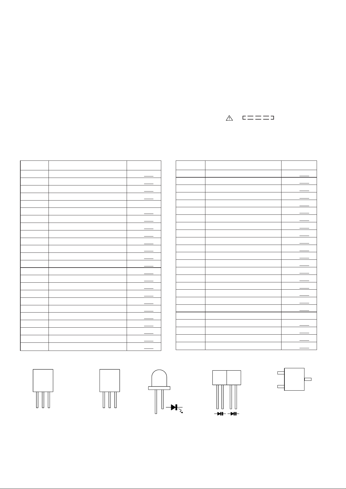
2SC1845 F
2SC2236 Y
2SC2878 A
2SC2878 B
2SC535 C
2SD468 C
KRA102 M
KRA107 M
KRC102 M
FRONT
E
(S)
(1)
VIEW
C
(G)
(2)
B
(D)
(3)
KRC104 M
KRC107 M
KTA1266 GR
KTA1268 GR
KTA1270 Y
KTA1271 Y
KTA1273 Y
KTC3199 GR
KTC3203 Y
FRONT
VIEW
FRONT
VIEW
B
C
E
(D)
(G)
(S)
(3)
(2)
2SD2012
2SB1375
(1)
SLR325MG
SLR325VR
KL052UL
SLR505MC
LMKD515B
Figure 16 TYPES OF TRANSISTOR AND LED
– 16 –
FRONT VIEW
KV1236Z23
2
FRONT
VIEW
3
1
KRA107 S
KRC102 S
KRC107 S
Page 17
8
27
1
2
3
4
5
98
6
7
20
12
13
242530
31
3222
34
35
36
10 11
272628
29
PU-IN SW
XL1
XIN
LD0
FIN2
JP–
CV+
SLC
SL1
FIN1EF
TO
FD
SPO
NC
SLD
SL–
SL+
DRF
CL
DAT
CE
VCC1
6
+5V
PICKUP IN
SW4
FOCUS COIL
TRACKING COIL
M1
DISC
MOTOR
M
M
M2
SLIDE
MOTOR
PICKUP UNIT
9
IC2
LC78622K
SERVO/SIGNAL
CONTROL
+B1
IC3
M56748FP
DRIVER
IC1
LA9241M
SERVO AMP.
6
1
9
5
+B1
+12V(+B6)
RES. CQCK. COIN
SQOUT. RWC. WRQ
~
~
~
CL, DAT, SELIAL CONTROL/CE
Q93
Q91
Q91
SL+. SL–. DRF
7
3
9
8
7
6
5
4
3
2
1
GND (D)
MECHA UP
GND (D)
DISK NO.
OPEN/CLOSE
GND (D)M–M+
GND (M)
9
8
7
6
5
4
3
2
1
CNP10
M
+5V
+B8
62
64 45 3623 43
31
24
25
10 10
265853
101220
324043
44
5352515431302923271615
4144
Q1
Q52
+4.3V
Q81 +7.3V (+B8)
REGULATOR
TO MAIN SECTION
IC81
TA7291S
LORDING MOTOR
DRIVER
XOUT
EFMO
EFMIN
CLV+
JP–
CONT2
CONT1
CONT4
DOUT
VVDD
VDD
LVDD
RVDD
XVDD
SW1
OPEN/CLOSE
SW2
MECHA UP
SW3
DISC No.
M3
LOADING
SOLM1
TO MAIN
SECTION
CNS10
CD-K491W
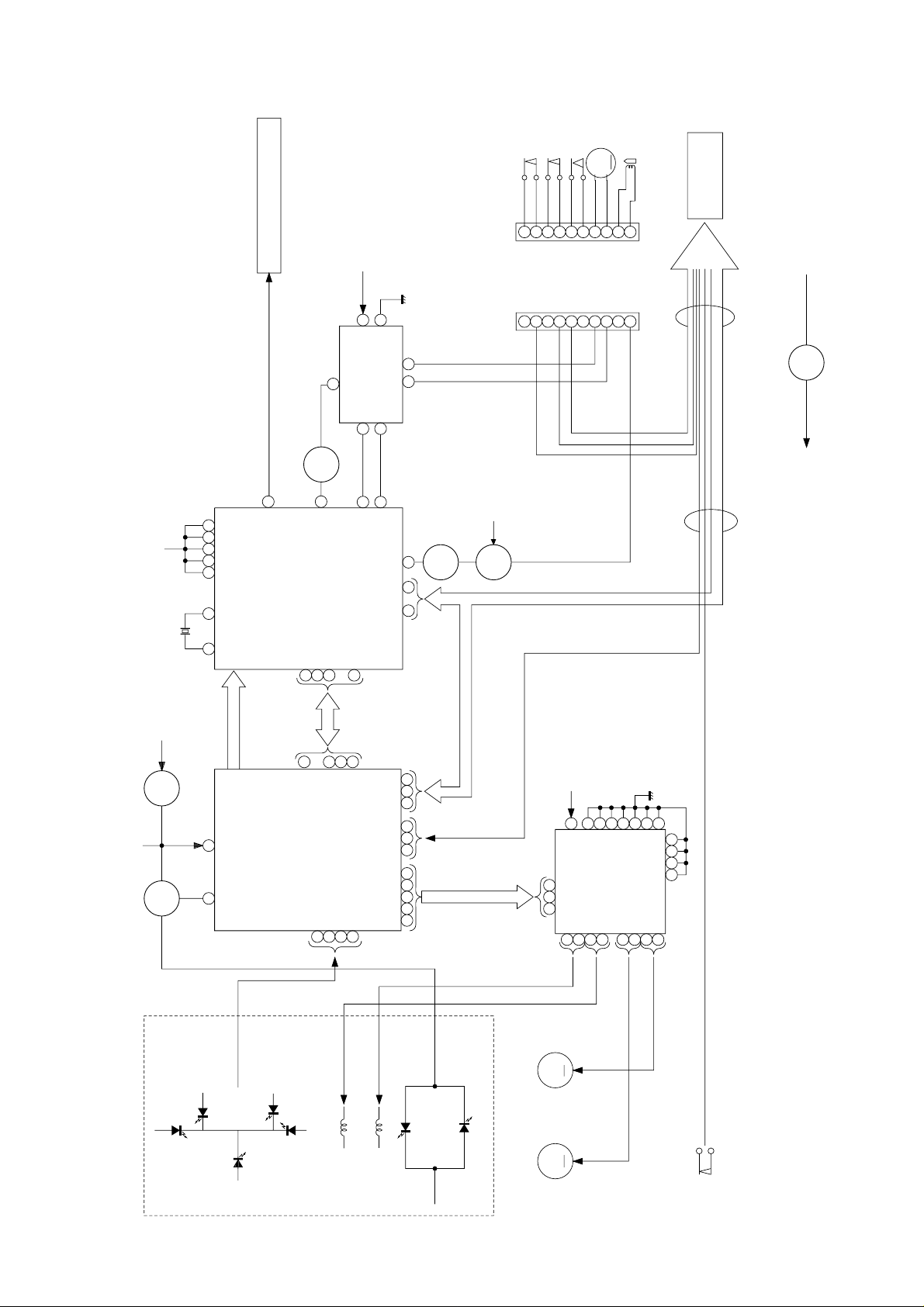
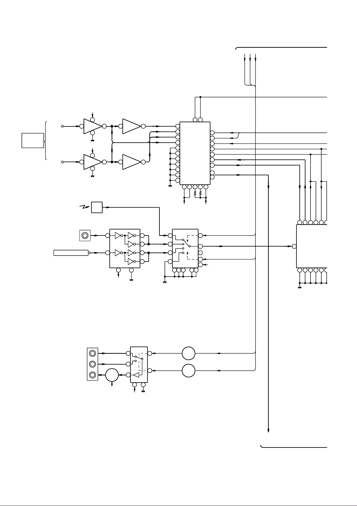
Figure 17 BLOCK DIAGRAM (1/5)
– 17 –
Page 18
CD-K491W
5
6
ANAROG RCH
TO
MAIN
SECTION
ANAROG LCH
LOW PASS FILTER &
DIFFERENTIAL AMP
2
IN
A-GND
2 1
IN
A-GND
LOW PASS FILTER &
DVD2
DIGITAL
IN
JA11
DVD2
DIGITAL
IN
FROM CD UNIT
ICA12
NJM4580M
+B7
8
4
+B7
8
4
IN
1
6
AINR–
OUT
AINL–
IN
6
ICA11
NJM4580M
DIFFERENTIAL AMP
TOS
ICA14
GP1F38R
ICA15
TC74HCU04
INVERTER
IN
1 4
IN
13
14
7
+B13
D4-GND
OUT
7
7
6
8
10
AINL+
OUT
AINR+
3
AINR–
4
AINL+
5
AINL–
6
2
8
18
19
20
22
25
A-GND
ICA16
TC74HCU15
SWITCH
IN
3
IN
4
IN
5
8
1
D4-GND
11
6
ICA13
1
7
~
13
PWDA
PWAD
23
24
16
17
15
11
12
13
A/D,D/A
AK4520A
14
CONVERTER
27
26
21
10
9
+B13+B9
14
D-OUT
7
9
2
+B13
16
15
DEM0
DEM1
SCK
CLK
CLK2L/R
SL/SR IN
D-OUT
LS OUT
RS OUT
DGTL2
DGTL1
DGTL1
DGTL2
V1/V2
D-IN
D-IN
SL/SR OUT
83
79
61
36
4
D3-GND
CLK2L/R OUT
CLK2OUT
9
97
92
91
85
62
8
60
JH51
VIDEO1 IN
VIDEO2 IN
MONITOR
OUT
QH51
+B7
ICH51
NJM2246M
SWITCH
1
3
7
2
4
8
6
+B7
V-GND
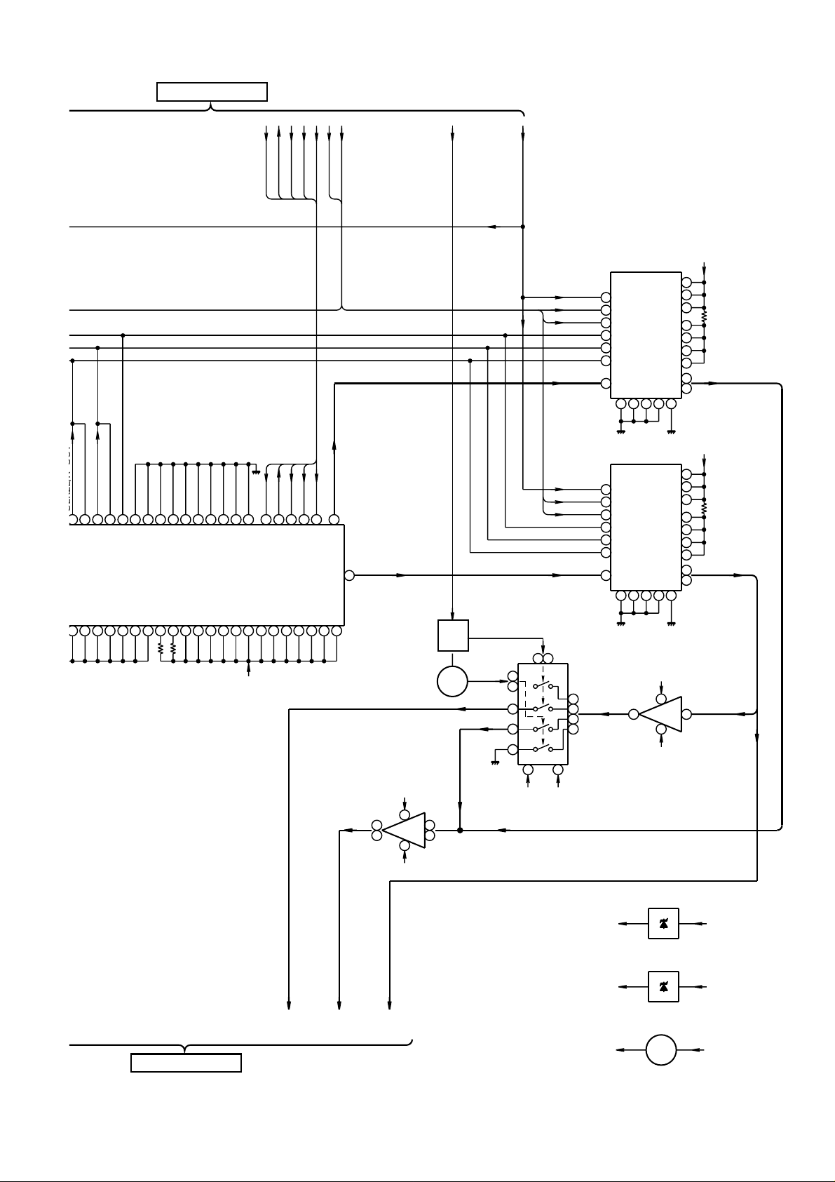
Figure 18 BLOCK DIAGRAM (2/5)
– 18 –
SWITCHING
DGTL2
QH53
QH52
SWITCHING
V1/V2
DGTL2
V1/V2
LS/RS
OUT
Page 19
CLK2L/R
OUT
TO MAIN SECTION
SSSOSCK SIDEMO1
DEMO0
AC3 RESET
SUB
ON/OFF
WOOFER
CD-K491W
AD RESET
+B12
97
1
62
0
SCK
CLK
CLK2L/R
CLK2OUT
SCK2IN
95
66
92
94
85
86
44
53
29
19
8
2
37
GND
65
ICA18
ZR38600
DOLBY AC-3 /5.1
MPEG2 AUDIO
DECORDER
48
78
90
5
30
12
17
6
D3-GND
68
71
VDD
45
35
+B13
SSSORESET
34
82
87
3
70
55
59
67
FL/FR OUT
SCK
SI
80
89
54
93
81
84
ICB01
NJM4580M
MIX AMP
CENTER
SUB
WOOFER
OUT
OUT
L
1
7
R
SUB
WOOFER
ON/OFF
SWITCHING
+B7
8
3
5
4
IN
–B12
QA01
QA02
QA03
MIX
SUB
WOOFER
OUT
A-GND
SUB
WOOFER
FL/FR
12
13
10
2
9
14
+B12
5
CENTER
WOOFER
6
7
–B12
FL/FR
SUB
PD
6
DEM0
12
DEM1
13
XT1
5
LRCK
9
7
8
ICA19
1
3
BICK
IN
D3-GND
PD
6
DEM0
12
DEM1
13
XT1
5
LRCK
9
BICK
ICA20
7
8
IN
1 3
D3-GND
ICA21
NJM4580M
–15dB AMP
4
1
8
11
7
ICA22
BU4066BCE
SWITCH
16
20
22
2
14
D/A
15
AK4321
24
CONVERTER
18
17
11
21
10
A-GND
16
20
22
2
14
D/A
15
AK4321
24
CONVERTER
18
17
11
10
21
A-GND
+B7
8
5
4
–B12
FL
FR
OUT
+B12
CENTER
SUB
WOOFER
SUB
WOOFER
IN
TO MAIN SECTION
SUB
WOOFER
OUT
FL/FR
OUT
CENTER
OUT
Figure 19 BLOCK DIAGRAM (3/5)
– 19 –
+B12
+B13
VOLTAGE
REGURATER
VOLTAGE
REGURATER
QB01
VOLTAGE
REGURATER
UN-SWITCHED
–B6–B12
+B7
+B9
Page 20
CD-K491W
4
1
RIN
PASS FILTER
SO301
ANTENNA
TERMINAL
FM
GND
SW1
SW2
MW
T302
MW ANT.
FM BAND
BFT01
231
MW OSC.
T306
1
TA7358AP
FM FRONT END
38
5
FM
LT01
SW1/SW2
ANT.
T303
T304
Q308
Q309
ICT01
RF
LT02
T307
T308
FM
OSC
SW1/SW2
OSC.
QT01
Q306
Q307
7
6
9
AMP
SW1 +B
SW2 +B
FM +B
MW +B
FM IF
TT01
Q360
Q362
FMOSC
+B7
+B7
FM IF
CF302
FM IF IN
VR351
FM MUTE LEVEL
X352
4.5MHz
FM
7
20
+B7
Q363
+B7
AM IF
T351
321
REGOUT
FM IF DET./FM MPX./AM IF
AM OSC
IN
AFC
OUT
AM IN
AM IN
1
OSC
LC72131
PLL CONTROLLER
9
+B7
Q364
7
STEREO
AM RF IN
FM IN
IC302
CE
AM IF
CF352
IC303
LA1832
FM MONO/ST MONO/ST
1011161522
43
5
DI
CL
4
IN
IF OUT
IF IN
2113
6
DO
FM IF
CF351
GND
VOLTAGE
REGURATER
+B7
+12V
1712
VCC
985
Q361
8
+B7
X351
456KHz
17
16
18
OUT
IN
SD
1561412101321222324
RL
MUTING
Q353
Q354
ICH11
MOTOR
DRIVE
8
+B7
ICH11
MOTOR
DRIVE
4
-B6
7
2
SPE IN
6
1
JR11
VCR/AUX1
JR12
VCR/AUX2
TAPE 1
TAPE 2
L
L
MM1
TAPE
MOTOR
SWM3
REC FWD
SWM6
CAM SW
SWM5
T1 RUN2SW
SWM4
REC REV
SWM1
T1 CrO
SWM2
T2 CrO
SOLM1
SOLENOID
PB HEAD
REC/PB
M
L-CH
R-CH
HEAD
L-CH
R-CH
R
R
PHM1
2
2
ERASE
HEAD
MOTOR
DRIVER
+B6
P.B
+B2
QL14
SPEED
DRIVER
REC
AC BIAS
DRIVER
VRM1
TAPE
QL15
QL19
P.B
QK03 QK05
QK04 QK06
QK17 QK18
DRIVER
REC/PB
QK09
QK10
QL18
QL12
QL13
SWITCHING
QL17
QL11
QL16
T1/T2 SOLENOID
PLAYBACK&RECORD AMP
L(T1)
R(T1)
L(T2)
R(T2)
L NF
R NF
POP REDUCE
L REC
R REC
QK07
REF
QK08
+B7
QK11
QK28
LK04
QK31
QK32
BIAS OSC.
TA MOT SW
HI SPEED
TA MOT H/L
T22RUN
T2 FWD-REC
CAM SW
2
T1/T2 CrO
T2 REV-REC
2
T1 Cr0
T2 Cr0
2
ICK01 AN7345K
1
P.B.
24
2
23
3
4
T1/T2
H/N
6
REC
9
16
14
13
NOR/
T1/T2
12
HIGH
15 19
P.B
L
4
21
R
5
20
L R REC
7
18
8
17
ALC
10
SWITCHING
QK25
QK13
QK14
L NF
R NF
SWITCHING
2
Cr0
TC4052BF
DUAL 4CH ANALOG
MULTIPLEXER
PB MUTE
QK17
QK18
MUTING
REC MUTE
QK21
QK22
MUTING
SWITCHING
HI SPEED
QK15
QK16
QK19
SWITCHING
SWITCHING
BAIS
QK26QK24
QK27
BEAT CHANCEL
ICZ08
T1/T2
REC/PB
Cr0
TUNER
TAPE
VCR 1
VCR 2
PB-EQ
BAIS
2
FUNC-A
10
L
12
1
R
L
14
R
5
L
15
2
R
L
11
4
R
7
–B10
LEVEL SHIFT
QK29
QK40
SWITCHING
QK30
QZ03
QZ04
FUNC-B
9
L
13
3
R
16
+B10
ICZ09
NJM4565M
LINE AMP.
–B10
L
R
IN
3
5
4
8
+B10
1
7
OUT
L
R
TO DOLBY SECTION
QG04
J602
MIC2
J602
MIC1
DET
VOICE C
MIC
1
IN
6
MIC2 IN
MIC SW
31
MIC1
VOL IN
5
VR602
MIC2
VOLUME
33 34
Q631
VOLTAGE
REGULATOR
19 18
VCCMIC
IC601
M65845FP
MIC AMP.
MIC2
VOL IN
10 25
VR601
MIC1
VOLUME
+B7
GND
OUT
ECHO
VOL IN
VR603
DIGITAL ECHO
VOLUME
26
IN
27
L
29
28
R
L-OUT
20
40
L-IN
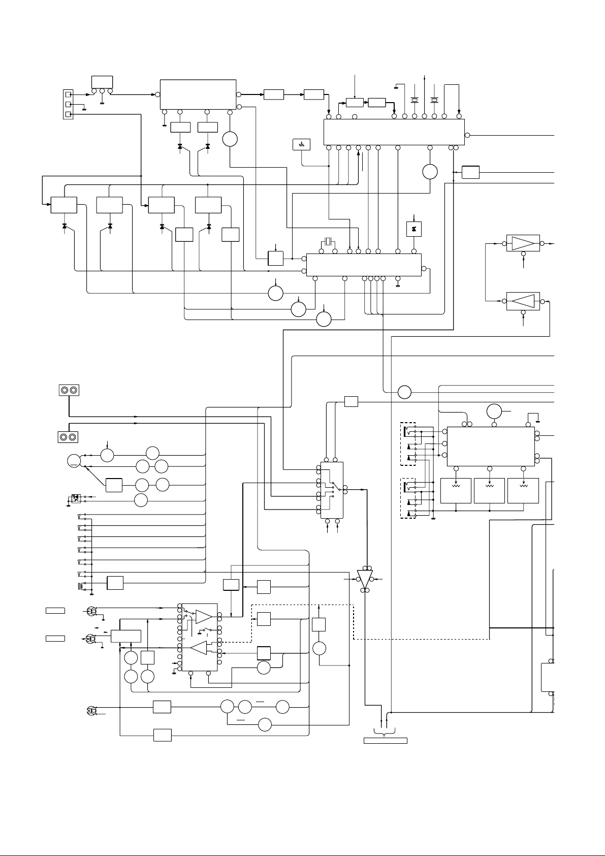
Figure 20 BLOCK DIAGRAM (4/5)
– 20 –
Page 21
CD-K491W
F1
1
7
5
VEE
SWD01
JOG SW
–VP
QV18
QX13
QX14
QY51
F995
F997
T2.5A L 250V
F998
T1.6A L 250V
VOLTAGE
REGULATOR
VF2
(AC)
SWD02
QX51
F1
F2
F2
QV19
RLYX11
RLYY51
RELAY
TRANSFORMER
FD01
+B2
RXD01
REMOTE
STB
RES
SCK
10
8
9
S-MUTE
S-W RELAY
CENTER RELAY
SURROUND RELAY
C-MUTE
SR-MUTE
SW-MUTE
QR11
QR13
QR12
QP13
QP14
QP15
VOLTAGE
REGURATER
VOLTAGE
REGULATOR
Q903
VOLTAGE
REGULATOR
Q902
Q901
Q906
Q905
Q904
SWITCHING
VOLTAGE
REGULATOR
Q909
Q908
SENSOR
RES
STB
DAT
COM
SCK
RES
99
CQCK
5
COIN
3
SQ OUT
4
WRQ
11
RWC
100
CD SL+
2
CD SL–
1
CD-PUIN
14
CD-DRF
13
18
56
VDD
90
15
VSS
57
89
RESET IN
12
16
17
SYSTEM STOP
28
CD O/C
86
CD U/D
85
CD DNO
84
7666656463545251
POWER
S-W-MUTE
CENTER-MUTE
SURROUND-MUTE
POWER
QV16
QV17
L-IN
QP11
QP12
R-IN
C-IN
SL-IN
SR-IN
SW-IN
QX17
QX18
QP17
–12V
F999
T500mA L 250V
29
12
1
95
96
97
+B4
OSC
X201
4.19MHz
SWITCHING
16
ICV01
12
STK407-27
POWER AMP.
18
16
12
ICX01
STK407-27
POWER AMP.
18
SWITCHING
Q913
Q914
REGULATOR
4
3
,
10
8
~
8885
~
91 94
~
LEDD01~
LEDD23~28
+B3
+B4 (5V BACK UP)
RESET
QG01
P.FAIL DET
POSISTOR
14
7
+B
–B
5
3
+B
–B
5
3
14
+B
–B
D991
VOLTAGE
Q911
Q910
TO DOLBY SECTION
TUNER MUTE
L-IN
R-IN
C-IN
SL-IN
SR-IN
SW-IN
SR-OUT
1545444241
SR-IN
+B7
SPE1~5
T1 RUN
T2 RUN
T2 A FP
T2 B FP
T1 CrO
T2 CrO
CAM-SW
TAPE SOL
TA MOT
HIGH SP
FR SP
BIAS
BEAT CUT
TA R/P
TA PB EQ.
REC MUT
T1/T2
PB MUTE
VOICE-C
MIC DET
VR ST
39
17
16
11
ICZ10
M62446FP
9
8
ELECTRO-
6
VOLUME
ICZ02,04,06
1
NJM4565D
IN/OUT
FILTER
AMP
ICZ01
LC7522
G.E. VOL
ICZ03,05,07
1
NJM4565M
IN/OUT
FILTER
AMP
13
12
9
10
31
+B7
VOLTAGE
REGURATER
TU-SD
TU-DO
AD RES
CE1
~
19
2362615560 78 79
29
30
31
32
2
33
2
34
35
36
37
38
39
SYSTEM MICROCOMPUTER
40
41
42
43
44
45
46
77
81
FUNC A
VR ST
L-OUT
31
32
R-OUT
C-OUT
33
SL-OUT
34
35
SR-OUT
SW-OUT
36
30
5
42
8
4
16
1
17
14
8
4
VR CLK
VR DATA
–B10
+B10
+B11
+B10
–B10
+B10
–B10
+B10
–B10
585969707167
53
DI
TU CL
CLK2
DI
CLK
68 4748
FUNC B
VR CLK
VR DATA
40
41
6ch
NIC
BYP
AC3_SI
DIGITAL2
AC3_RES
DIGITAL1
SP CONF
AC3_SS
87 88 919293
ICF01
IX0254AW
AMP
QS2AC
VOLT SW
QS2SPRED
–B6
–B10
+B2
+B6
+B7
MO
AR
+B10
AC
+B8
TO CD UNIT
+B9
+B12
AC3_SCK
AC3_SO
94 95
737475
QS2MO
H/P SW
IN
L
R
REGULATOR
DEM 1
V1/V2
DEM 0
COM
96
98
97
6
50
2482
492726
FAN
PROT
SP LEVEL
POSISTOR
FRONT RELAY
+B7
OUT
8
5
7
3
1
4
ICP11
NJM4565M
LOW BOOST AMP.
–B6
–15V
VOLTAGE
REGULATOR
QZ01
+4.6V
UN-SWITCHED
+12V(MOTOR)
VOLTAGE
REGULATOR
+12V(ANALOG)
QZ02
VOLTAGE
+7.3V(CD)
+5V(AC-3)
VOLTAGE
QP91
REGULATOR
DAT
7
S-MUTE
QP13
QP14
QP16
L
R
1
R
E
7
1
R
E
2
SPE IN
18
D
26
IN
27
L
29
UT
28
R
3
CHO
E
L-OUT
R-OUT
C-OUT
SL-OUT
1617181920
ICQ01
QS7777PF
Q-SOUND
40
L-IN
R-IN
C-IN
SL-IN
FL DIPLAY
39 53
31
5
~
,
2
7
4
3
5
0
0
5
4
5
~ ~ ~ ~
ICD01
IX0233AW
SYSTEM
MICROCUMPUTER
VDD VSS
158918
4672 90 51 13142728
+B2
+B6
MEMORY
BACK UP
QG02
+B3
QG03
ZDF01
FAN
H/P SW
SP DET
RELAY
PROT
QV13
QV14
QY11
L-OUT
9
8
R-OUT
20
1
C-OUT
7
SL-OUT
9
SR-OUT
8
20
SW-OUT
1
D992~D995
D996~D999
VF1
(AC)
~
7
3
7
1
+5V
UNSWITCH
+B2
T8A L 250V
T8A L 250V
Q951
–VP
F996
2
62
57
16
17
21
26
~
QX16
POWER
T991
XD01
KEY IN
TO CD UNIT
QV22
QY21
RLYV11
RLYY11
RELAY
QY52
QX20
T.F
VF2
(AC)
VF1
(AC)
KEY MATRIX
SWD03~SWD06
SWD12~SWD17
SWD23,
SWD26~SWD43
SWD50~SWD54
+B6
QV20
QV21
+
–
+
–
+
M
M901
FAN
MOTOR
JV91
HEADPHONES
TMV01
SPEAKER
TERMINAL
L-CH
GND
R-CH
GND
C-CH
–
GND
+
SL-CH
GND
–
+
SR-CH
–
SW-CH
+
GND
–
GND
TMV01
SPEAKER
TERMINAL
230~240V
F992
T2.5A L 250V
220V
127V
110V
AC POWER
SUPPLY CORD
AC110/127/220/230-240V
50/60Hz
F991
T2.5A L 250V
SW991
VOLTAGE
SELECTOR
F991
T5A L 250V
Figure 21 BLOCK DIAGRAM (5/5)
– 21 –
Page 22
CD-K491W
3
2
C
2
SQ OUT(DSP)
A
B
C
LT0H30M1
D
TR+
FO+
FO–
TR–
ACTUATOR
LD
LD
K
E
B
GND
A
F
C
2200P
1M
MON
1M
2200P
CNS1B
K
5
E
4
A
3
B
2
F
1
CNS1A
1
2
3
4
5
R2
1K
R13
C2
1K
TE
R14
27K
3.3K
1.5V
0.01
C85
0.001
C54
R11
6.8K
R12
100
R16
R21
22K
C12
0.1
C4
0.1
C1
47/16
4.8V
Q1
4.2V
KTA1266 GR
9
R8
R9
15K
100
R10
0.033
2.2K
0.001
C8
0.068
C9
0.047
R15
12K
C10
180P
8
1K
R20
R22
22K
2.5V
C5
C6
0.033
C7
0.1/50
2.5V
2.5V
2.4V
2.5V
2.5V
2.5V
1/50
2.4V
2.4V
2.4V
2.5V
NC
2.5V
R19
R1
10
C3
2.5V
2.5V
2.5V
C11
0.1
1K
2.5V
1
2
3
4
5
6
7
8
9
10
11
12
13
14
15
16
R17
33K
VREF
VCC1
FIN2
FIN1
E
F
TB
TE–
TE
TESI
SCI
TH
TD–
TD
JP
TO
FD
R18
15K
REF
REF
1
4.8V
C33
C34
0.33/50
0.47/50
C32
0.01
560
R46
1V
0V
4.2V
2.2V
–
BHI
LDS
LDO
+
RF
–
+
–
–
+
+
REF
–
+
REF
–
+
REF
+
–
REF
REF
–
+
REF
+
GEN
–
TO
REF
+
REF
GEN
–
REF
+
–
+
–
FA
FD–
19
18
17
2.5V
2.5V
2.5V
R23
10K
R24
47K
1V
PHI
FE1
REF
VCR
VCR
–
VCR
+
VCR
+
–
+
TGL1
–
THDL
JP
FSC
FOSTA
REF
GEN
+
–
REF
+
–
AGND
FE
FE–
FA–
2.4V
C13
C14
0.01
20
330P
R25
1.5K
21
R26
82K
SP
22
0V
2.5V
C30
C31
0.1/50
220/6.3
4.8V
2.5V
2.5V
VR
LF2
REF1
+
–
REF
+
DEF
–
–
+
HFL
+
DRF
–
IC1
LA9241M
SERVO AMP.
VCC
+
–
REF
+
–
REF
GL
FSTA
REF
S.Q.R
THD
+
–
REF
FE1
+
–
REF
SP–
SPI
SPG
2423
26
25
2.5V
2.5V
2.5V
10K
C16
R28
0.0047
R29 56K
R31
1.2K
R27
39K
C18
0.47/50
VCC2
JP
C17
R30
SPO
27
2.5V
0.001
6.8K
4.8V
FSS
EFBAL
FOSTA
TOSTA
2FREQ
LASER
FSTA
8/12CM
SLOF
+
–
+
–
10
REF
SLEO
28
2.5V
0V
DRF
R33
1.2K
C20
CE
DAT
CV–
CV+
JP–
JP+
JPCLO
SLOF
OR
REF
47/16
R34
22K
4V4V0V
CL
CE
CL
LATOH
SLOF
SLOF
SLD
C19
1/50
R32
10K
REF
+
–
29
2.5V
0V
2.4V
49505152535455565758596061626364
0V
NC
48
R45
JP–
32
SLI
0V
C21
47
46
45
44
2.5V
43
2.4V
42
1.5V
41
40
39
38
37
36
35
34
33
R36
0.0033
220K
2.5V
0V
2.4V
C27
HF
TP1
0V
0V
4.8V
4.8V
0V
6
R37
82K
0V
4.8V
2.5V
0.001
R40
5.6K
C24
2.2P
4.7K
0V
C35
1/50
C29
7
GND
4.7/50
C26
0.033
R41
47K
C25
27P
R43
56K
C28
0.1
R44
33K
R42
47K
R38
470
R39
1K
1SS133
C2
0.00
D1
CLK
DEF
TBC
2
FSC
DGND
REF
+
–
SLC
3
RFS–
+
–
RFSM
RF
CV+
4
CV–
SLOF
HFL
5
TES
TOFF
TGL
+
–
JP+
SL–
SL+
30
31
2.2V
2.2V
R35
220K
C15
0.01
K
1
A
2
B
3
E
4
F
5
CNP1
K
5
E
4
A
3
B
2
F
1
TR–
1
TR+
2
FO+
3
FO–
4
GND
5
PD
6
VR
7
LD
8
PICKUP UNIT
E
CNS2B
TR–
1
TR+
2
FO+
3
FO–
4
GND
5
6
PD
VR
7
LD
8
F
+
M1
M
Spindle
Motor
G
Pickup
M2
Sled
Motor
SW4
In
M
–
+
–
6
5
4
3
2
1
CNS3B
CNP3A
6
5
4
3
2
1
CNS2A
1
2
3
4
5
6
7
8
CNS3A
6
5
4
3
2
1
1
2
3
4
5
6
7
8
CNP2
CNP3
6
5
4
3
2
1
PD
LD
TR–
TR+
FO+
FO–
CD2GND
SP+
SP–
SL2+
SL2–
CD2PUIN
C36
100/16
2.5V
1
2.5V
2
0V
3
2.5V
4
2.5V
5
2V
6
2V
7
0V
8
0V
9
0V
10
IC3
0V
11
0V
12
2V
13
2.5V
14
2.5V
15
0V
16
4.7V
17
0V
18
36
0V
35
0V
34
0V
33
2.5V
32
2.5V
31
1.8V
30
1.8V
29
0V
28
0V
27
0V
26
0V
25
2V
M56748FP
/SLIDE DRIVER
FOCUS/TRACKING/SPIN
2.5V
2.5V
2.5V
4.7V
0.7V
R48
24
2V
10K
23
22
21
20
19
+B
CD MOTOR PWB-K
12
+B
D3
RL104A
D2
RL104A
CNP12
D4
RL104A
RWC(DSP)
1
WRQ(DSP)
CO IN(DSP)
2
3
H
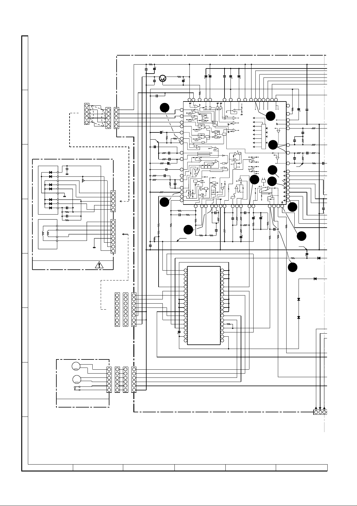
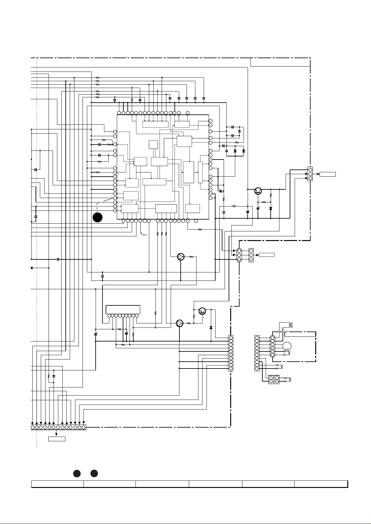
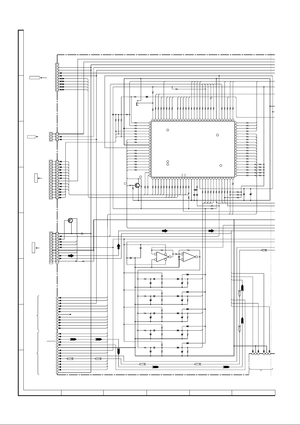
• NOTES ON SCHEMATIC DIAGRAM can be found on page 16.
1
23456
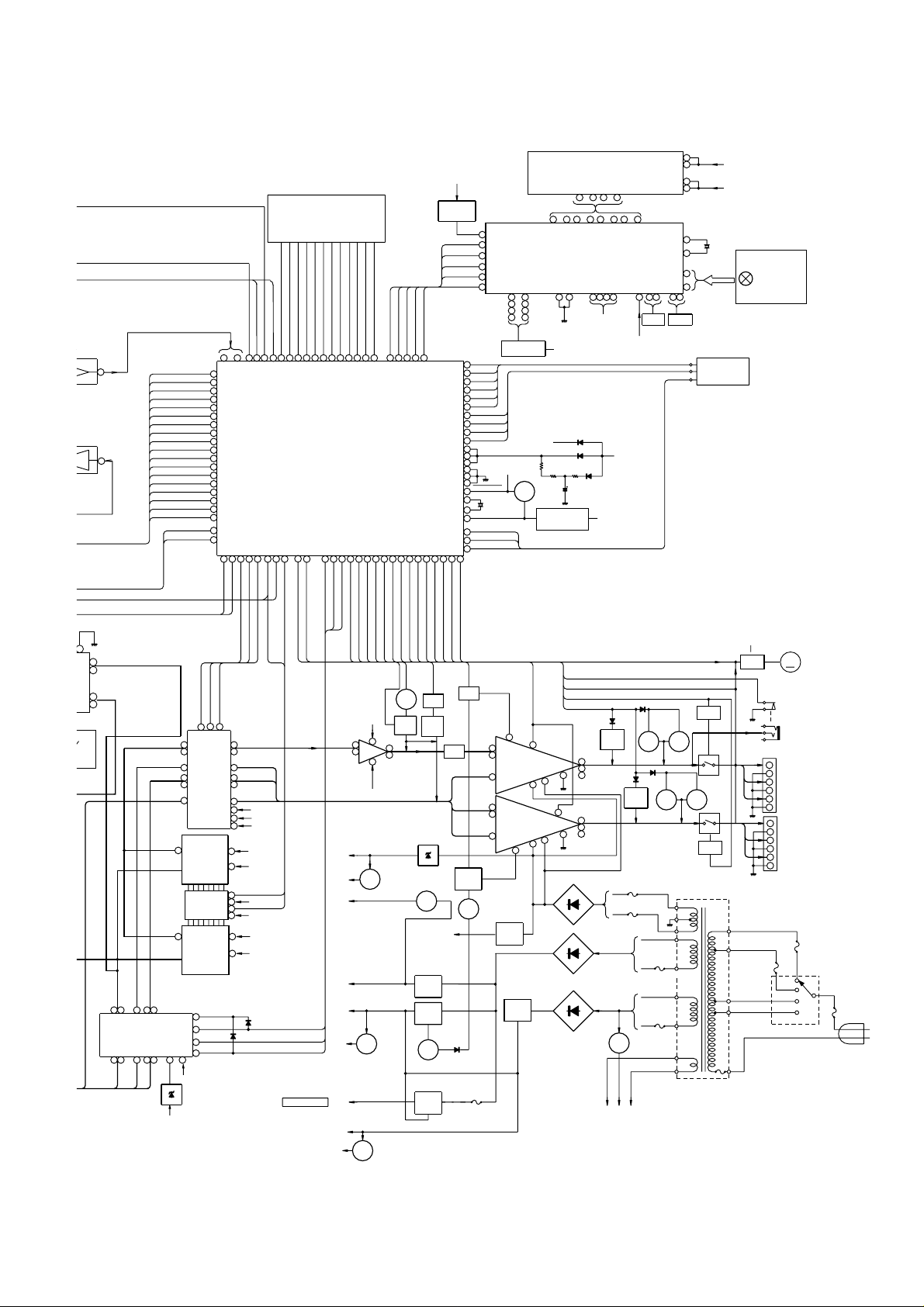
Figure 22 SCHEMATIC DIAGRAM (1/20)
– 22 –
Page 23
C23
WRQ(DSP)
0.0027
1
S133
A
C22
220P
R47
10K
C57
0.001
C37
0.022
R57 1K
R58 1K
R59 1K
R61 1K
C39
0.047
0.047
R52
27K
R53 1.2K
11
R62 1K
R63 1K
R51
3.3M
R50
680
C40
4.8V
2.5V
C38
0.01
0V
0V
1.9V
0V
0V
2.5V
0V
4.8V
0V
0V
0V
0V
0V
R60
1K
/CS
TEST5
TEST1
DEF1
1
TA1
2
0V
PDO
3
VVSS
4
ISET
5
VVDD
6
FR
7
VSS
8
EFMO
9
SLICE LEVEL
EFMIN
CONTROL
10
TEST2
11
CLV+
12
CLV
CLV2
DIGITAL SERVO
13
V/P
14
HLF
15
SERVO
TES
COMMAND
16
TOFF
TGL
17
18 19 20 21 22 23 24 25 26 27 28 29
4.8V
0V
4.8V
IC2
LC78622K
SERVO/SIGNAL
CONTROL
C56
0.022
CD2LD2M–
+B
IC81
TA7291S
LOADING MOTOR DRIVER
0V
6.4V1V0V
6.5V
6.5V
6.5V
4 3 2 1
6
5
7
NC
3.9
C82
47/16
R83
C81
47/16
R85
56
(1/2W)
C46
NC
NC
4M
16M
/RES
/CQCK
TEST11
INTERFACE
VCO CLOCK
OSC CONTROL
SYNC-DETECT
EFM DEMODULATE
JP+
JP2
PCK
FSEQ
0V
0V
2.5V
4.8V
NC
R81
2.9V
0V
3.9K
8
9
R82
6.8K
100P
FSX
COIN
RWC
SQOUT
WRQ
µ-COM
2Kx8
RAM
ERROR COERECT
FLAG CONTROL
EXTERNAL
OUTPUT
VDD
CONT1
CONT2
CONT3
CONT4
0V
0V0V0V
R88 1K
R90 1K
R89 1K
0V
CD2LD2M+
C45
C44
100P
NC
NC
SFSY
SBCK
SUB-CODE
X-TAL
GENERATOR
DIGITAL
FILTER
CONT5
C2F
EMPH
30 31
NC
NC
NC
0V
0V
4.8V
Q51
KRC107 M
3
1
0V
+B
Q93
KRC102 M
3
2
0V
0V
1
C47
100P
100P
NC
49505152535455565758596061626364
PW
4FS
DIGITAL
OUT
DOUT
2.5V
0V
2
R80
6.8K
12V
R86
2.2K
C48
100P
EFLG
SBSY
XVSS
XIN
XOUT
XVDD
MUTER
RVDD
RCHO
RVSS
LVSS
1BIT DAC
LCHO
LVDD
MUTEL
TEST4
TEST3
32
0V
NC
R54
330
Q91
KTA1271 Y
12V
12V
10K
R87
C49
100P
2.2V
48
47
0V
0V
46
2.1V
45
2.2V
44
4.8V
43
4.8V
42
4.5V
41
2.0V
40
0V
39
0V
38
0V
37
4.5V
36
4.8V
NC
35
34
33
0V
0V
D91
1SS133
CD2D2NO
M–
M+
C53
0V
R55
150
SOL
CNP10
0.022
C83
0.022
C43
330/6.3
+B
C41
12P
C42
15P
R93
220
0.82µH
C50
1
2
3
4
5
6
7
8
9
10
+B
D81
1SS133
L61
C51
0.022
100/16
+B
BI99
1
2
3
CNS99
SOL
GND(M)
M–
M+
GND(D)
OPEN CLOSE
DISC NO.
GND(D)
MECHA UP
GND(D)
CD SERVO PWB-B
XL1
16.934MHz
D82
1SS133
CD-GND
+7.3V
Q52
KTC3203 Y
+5V
1
2
TO MAIN PWB
3
1
2
3
4
5
6
7
8
9
10
CNS10
R64
22
C52
100/16
CNPR11
P28 2-C
BIM05
+7.3V
1 2 1
CNS5
R66
330
1
2
3
4
5
6
+B
ZD61
MTZJ4.7B
+B
SOLENOID 2
SENSOR PWB-J
–
M
+
SW2
MECHA UP
2
+12V
M3 T/T
UP/DOWN
LOADING
SW1
OPEN/
CLOSE
SW3
DISC
NUMBER
CD-K491W
1
2
3
CNP11
+B
LOCK
TO MAIN PWB
P24 1-C
CNSF11
OP/CLOS
UP/DOWN
CO IN(DSP)
SQ OUT(DSP)
234
D2GND
RES(DSP)
CQ CK(DSP)
DRF (ASP)
8
6
5
7
CNSF12
TO MAIN PWB
P24 1-D
SLD+
9
SLD–
PUIN SW
11
10
DISC NO.
12 13
14
• The numbers 1 to 12 are waveform numbers shown in page 52.
7
8 9 10 11 12
Figure 23 SCHEMATIC DIAGRAM (2/20)
– 23 –
Page 24
CD-K491W
A
CNPF01
10
GND(D)
9
8
TO
DISPLAY PWB
P36 1-C
CNSD01
GND(D)
+4.6V(D)
+12V(M)
COM1
RESET
DATA1
STB
SCK1
7
6
COM
5
RES
4
DAT
3
STB
2
SCK
1
B
TO
CD SERVO
PWB
P23 12-C
CNP11
GND(CD)
+7.3V(CD)
+12V(M)
CNSF11
1
2
3
BIF11
1
2
3
C
BIF12
CNSF12
RWC
11
WRQ
22
COIN
33
SQOUT
44
CQCK
55
66
RES
DRF
CNP12
DISC_NO
UP/DOWN
D_GND
SLD+
SLD–
PUIN
OP/CL
77
88
99
10
10
11 11
12 12
13
13
14 14
QG04
KTA1266 GR
TO
P23 7-H
CD SERVO PWB
D
GND(CD2)
GND(CD1)
GND(D)
+7.3V(CD)
+B
+12V(M)
+B
+4.6V(D)
+B
+B
RG11
1K
22K
@
@
RF76
RF77
POWER
VOICE-C
77
76
PF4
PF5
SCK
Si0
5
CQCK
SQOUT
1K
1K
RF04
RF05
10K
1K
1K
1K
1K
1K
1K
@
@
RF74
RF75
QS_AC
QS_SPRED
74
75
PF3
PF2
PL6
80
P06
1
P07
2
SI1
SO1
6
7
DAT
COM
RF07 1K
RF06 1K
1K
@
@
@
@
@
RF73
RF71
RF70
RF69
RF68
VR ST
VR CLK
VR DATA
FUNC B
QS_MO
73
72
70
6869
71
PF1
PF0
PE5
PE6
PE7
SYSTEM CONTROL
MICROCOMPUTER
SCK1
P17
P16
INT0
RES(MAIN)
10 11 12 131415
8
9
STB
DRF
SCK
RES
WRQ
DS_RES
1K
RF09 1K
RF10 1K
RF11 1K
RF12
RF13 1K
RF08 1K
RG04
GND(A)
1K
1K
1K
1K
100
1K
@
@
@
@
@
@
RF65
RF64
RF63
RF62
RF66
RF67
FUNC A
S.W.MUT
SYS_MUT
TUN_MUT CLCE1
CENT_MUT
REAR_MUT
PE0
PE1
PE2
PE3
PE4
IX0254AW
P74
PUIN
RF14 1K
10K
PD6
PD7
ICF01
VDD1
CF2
CF1
VSS1
P75
AN0
18 19 20 21 22 23 24 25 262728 29 30
16 17
VSS
0.0
RF17
SP_4K
1K
@
XF01
15P
CG05
RF19
CG06 15P
+B
1K
1K
@
@
RF61
RF60
TUN_SD
DO(TU)
(DI)PD5
AN1
SP_1K
SP_250Hz
1K
1K
@
@
RF21
RF20
RG38
100K
RG25
1K
1K
@
RF59
RF58
DI(TU,VR,PR)
58596061626364656667
57
PD2
PD4
(DO)PD3
AN2
AN3
AN4
SP_16K
SP_63Hz
1K
1K
@
@
RF22
RF23
@
10K
1K
@
RF55
VSS
VDD
5556
VSS2
VDD2
51
PC5
30
AN5
AN6
POSISTOR
TUN_SM
SP LEVEL
1K
10K
1K
@
@
@
RF25
RF24
RF26
PA0
PD1
AN7
1K
@
RF27
RG23
10K
10/100
SWF02
SPAN
SELECTOR
RG24
10K
10K
10K
10K
@
RG06
RF82
RF83
RF84
RF85
RF86
RF87
RF88
RF91
RF92
RF93
RF94
RF95
RF96
RF97
RF98
AC32SO
QG92
KTC3199 GR
7
SO
RG94
10K
RF81
1K
@
@
@
@
@
@
@
@
@
@
@
@
@
@
@
RG95
1K
1K
1K
1K
1K
1K
1K
1K
IC
@
@
RG07
RG08
+B
+B
+B
CFWU02
+B
1SS133
9/50
MIC_DET
1K
H/P SW
AUTO_SCAN
10K
CD_DNO_SW
1K
CD_U/D_SW
1K
1K
CD_O/C_SW
1K
DGTL1
1K
DGTL2
AC3_RES
AC3_SS
AC3_SIN
AC3_SO
AC3_SCK
V1/V2
DEM0
DEM1
94
10K
RG96
470K
DH06
VSS
VDD
RES
1K
@
RF99
RF80
RWC
1K
@
RG56
1K
81
82
83
84
85
86
87
88
89
90
91
92
93
94
95
96
97
98
99
10 0
10K
RG05
10K
@
RF79
9K/10K
SP_CONF
79
80
PL5
PL4
PL0
PL1
PL2
PL3
P30
P31
VSS3
VDD3
P32
P33
P34
P35
P00
P01
P02
P03
P04(PCCL)
P05
1234
SLD–
SLD+
1K
1K
RF02
RF01
1K
@
RF78
AD RES
78
PF7
COIN
1K
RF03
PF6
SO0
1K
1K
@
@
RF54
RF53
S.W.RLY
CLK2
5354
PD0
PC7
INT1
INT2
SP PROT
SYS_STOP
1K
RF28
1K
1K
@
@
RF52
RF51
CENT_RLY
REAR_RLY
51
52
PC4
50
PC6
49
PC3
48
PC2
PC1
47
46
PC0
45
PB7
44
PB6
43
PB5
42
PB4
41
PB3
40
PB2
39
PB1
PB0
38
PA7
37
PA6
36
35
PA5
34
PA4
PA3
33
PA2
32
PA1
31
INT3
RF30
1K
T1_RUN
T2_RUN
RG19
47K
RF29 1K
+4V(µ-CON)
GND(µ-CON)
FRNT_RLY
FAN CONT
VOLT_SW
AMP
PB_MUT
TA_T1/T2
REC_MUT
TA_PB-EQ
TA_R/P
BEAT CUT
TA_BIAS
FR SPEED(M)
HIGH_SP
TA MOTOR
TAPE_SOL
CAM_SW
T2_CRO S
T1_CRO S
T2_B-FP S
T2_A-FP S
+B
RG16
47K
RG26
10K
RF50 1K
RF49 1K
RF48 1K
RF47 1K
RF46 1K
RG55 1K
RF44 1K
RF43 1K
RF42 1K
RF41 1K
RF40 1K
RF39 K
RF38 1K
RF37 1K
RF36 1K
RF35 1K
RF34 1K
RF33 1K
RF32 1K
RF31 1K
0.022
CG56
CG57
RG17
RG15
47/25
+4V
10K
RG20 10K
RG21 10K
RG22 10K
10K
+B
+B
+B
+B
E
F
G
H
CNP303
P33 12-A
TUN MUTE
TO TUNER PWB
P27 12-B
TO MECHA SECTION
P27 12-E
TO DECK SECTION
GND(D)
CL
DO
CE(CE1)
DI
+12V(A)
GND(A)
L-CH
10
R-CH
11 11
SD
TA_FR SPEED
TA_MOT_SW
M +12V
TA_SOL
T2_A_FP
TA_CAM_SW
M_GND
T1_RUN
T2_RUN
T2_B_FP
T1_CrO
T2_CrO
TA_T1/T2
PB_MUT
PRE L-CH
HIGH_SP
PRE R-CH
GND(A)
+12V(A)
TA_BIAS
REC L-CH
REC R-CH
TA_R/P
REC_MUT
BEAT_CUT
TA_PB-EQ
GND(D)
BIF13
CNSF13
1
1
22
33
44
55
66
77
88
99
10
1
2
3
4
5
6
7
8
9
10
11
2
2
12
13
14
15
16
17
18
19
20
54
55
23
24
25
26
27
+12V(A)
GND(A)
M2GND
CG08
0.001
RG01
220K
TUN L
+B
+B
+B
–B
+B
CH29
0.022
–B
+B
+B
CH28
RH17
1.5K
CH30
0.0056
(ML)
RH20
1.5K
CH16
RH25
1.5K
CH19
0.47/50
RH30
1.5K
RH35
1.5K
CH25
0.027
0.022
1/50
CH22
(ML)
(ML)
0.1
+12V(A)
–15V
CH13
330P
CH17
0.047(ML)
CH20
0.015
CH23
0.0047
CH26
0.0012
+B
RH11
150K
2
–
8
1
(1/2)
4
+
3
–B
RH14
560K
RH15
33K
RH21
560K
RH22
33K
RH26
560K
RH27
33K
RH31
560K
RH32
33K
RH36
560K
RH37
33K
RH12
1K
6
47P
CH10
5
MOTOR DRIVER
DH16
1SS133
DH11
1SS133
CH15
0.22/50
DH12
1SS133
CH18
0.22/50
DH13
1SS133
CH21
0.22/50
DH14
1SS133
CH24
0.22/50
DH15
1SS133
CH27
0.22/50
RH13
150K
–
(2/2)
+
ICH11
NJM4558M
RH16
470K
DH17
1SS133
RH24
470K
DH18
1SS133
RH29
470K
DH19
1SS133
RH34
470K
DH20
1SS133
RH39
470K
7
16KHz
SPE-1
63Hz
SPE-2
250Hz
SPE-3
1KHz
SPE-4
4KHz
SPE-5
+B
GND(A)
REC L-CH
REC R-CH
PRE L-CH
PRE R-CH
TUN R
TAPE L
TAPE R
AUX 2
AUX 1
AUX 1
GND(A)
L-CH OUT
TO PRE SECTION
R-CH OUT
VIDEO2 IN VIDEO1 IN
P28 2-G
AUX 2
81
1885801884
GND(A)
L-CH OUT
+12V
–1
R-CH OUT
• NOTES ON SCHEMATIC DIAGRAM can be found on page 16.
1
23456
Figure 24 SCHEMATIC DIAGRAM (3/20)
– 24 –
Page 25
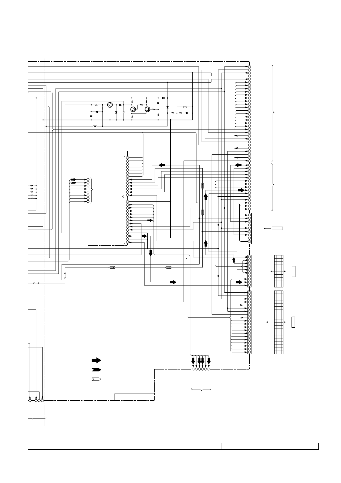
CD-K491W
+4V
RG17
10K
RG20 10K
RG21 10K
RG22 10K
RG15
10K
CD GND(D2)
CD GND(D1)
GND(D)
+7.3V(CD)
+12V(M)
+B
ZDF01
MTZJ3R3A
+4.6V(D)
+B
RESET
POINT
DG02
1SS133
RG30
RG29
CG01
150
150
470/10
+B
+B
+B
+B
–B
RESET
QG01
KRC102 M
RG37
1K
DG05
CG04
1SS133
0.01
LG01
TUN L
TAPE L
AUX 1
AUX 2
TUN R
AUX 1
AUX 2
2.2µH
78
15
80
81
82
17
84
TO VOLUME SECTION
85
P30 6-H
+B
TAPE R
+B
+B
2 3
1
RG36
3.3K
DG04
1SS133
CG03
RG35
3.3/50
1K
0.01
QG02
CG02
KTC3199 GR
+4V
VR CLK
67
VR DATA
68
VR LA TCH
69
CLK2
70
VR DI
71
FUNC A
72
FUNC B
73
54
55
58
56
57
76
P30 4-A
27
AC3-SW-CHOUT
76
AC3-RS-CHOUT
57
TO VOLUME SECTION
AC3-LS-CHOUT
56
AC3-C-CH OUT
58
AC3-R-CH OUT
55
AC3-L-CH OUT
54
SPEC ANA
77
–15V
28
+12V
19
AGND
18
LT IN
86
AGND
18
RT IN
87
RG34
10K
RG39
82
L OUT
R OUT
C IN(C OUT)
SL IN(LS OUT)
SR IN(RS OUT)
SW IN(SW OUT)
GND(D)
RG33
10K
RG32
100
QG03
KTC3199 GR
CONTROL
DG03
1SS133
RG31
1K
+B
+B
–B
+B
–B
+B
–B
+B
+B
+B
+B
–B
+B
+B
+B
–B
+B
–15V
28
GND(A)
18
+12V(A)
19
GND(D)
27
+4.6V(D)
29
SWF-MUTE
30
31
REAR-MUTE
32
CENT-MUTE
S-MUTE
33
AMP CONT
34
35
SW RLY(4)
36
REAR RLY(3)
37
CENT RLY(2)
38
VOLT SW
39
SP PROT
40
POSISTOR
41
H/P SW
42
SP LEVEL
43
FAN CONT
44
FRNT RLY(1)
45
POWER
+12V(M)
3
GND(M)
7
+7.3V(CD)
46
47
CD GND(D1)
48
CD GND(D2)
49
VGND
50
+5V(AC32A)
51
GND(D3)
GND(D4)
52
53
+5V(AC32B)
OUT(L)
54
55
OUT(R)
56
RL OUT
RR OUT
57
58
C OUT
59
C IN
RL IN
60
61
RR IN
62
IN(L)
63
IN(R)
18
GND(A)
+12V(A)
19
64
QS_SPRED
69
QS_AC
66
QS_MO
VCAN
1
OUT(L)
2
IN(L)
3
GND(A)
4
+12V(A)
5
OUT(R)
6
IN(R)
7
GND
8
MIC
9
P29 9-G
TO PRE SECTION
P31 7-H
TO QSOUND SECTION
FROM
KARAOKE
PWB
CNSU02
P32 3-A
X 2
1
188580
L-CH OUT
R-CH OUT
VIDEO2 IN IN
RE SECTION
P28 2-G
AUX 2
81
GND(A)
+12V(A)
–15V
R-CH OUT
FWA01
(AC3_B)
10
P35 8-H
CFWA01
TO DOLBY PWB
1
FWA02
20
P34 5-H
CFWA02
TO DOLBY PWB
1
CFWU01
SW IN(SW OUT)
10
C IN(C OUT)
9
L OUT(LIN)
8
SL IN(LS OUT)
7
R OUT(RIN)
+B
–B
–B
+B
+B
+B
FM SIGNAL
PLAYBACK SIGNAL
765756585554
6
SR IN(RS OUT)
5
AGND
4
V-SW(V1/V2)
3
LT IN
2
RT IN
1
A-15V
20
19
AGND
18
A+12V
17
+5V
16
VGND
+5V(AC3_A)
15
+5V(AC3_A)
14
13
GND(D3)
12
GND(D4)
11
DEM1
DEM0
10
9
SP CONF
8
DGTL1
7
SO
6
DGTL2
5
SS
AD RES
4
SI
3
AC3_RES
2
SCK
1
CFWU02
RECORD SIGNAL
AC3-C-CH OUT
AC3-L-CH OUT
AC3-R-CH OUT
AC3-LS-Ch OUT
AC3-RS-CH OUT
AC3-SW-CH OUT
TO PRE SECTION
MAIN PWB-A(1/5)
P28 4-G
7
8 9 10 11 12
Figure 25 SCHEMATIC DIAGRAM (4/20)
– 25 –
Page 26
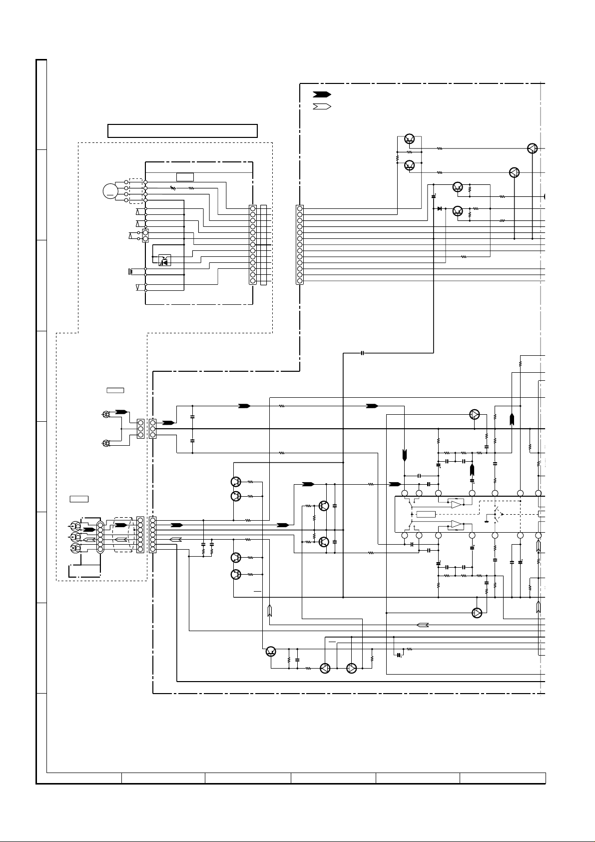
CD-K491W
CK31
CK29
7
M
G
R
G
A
B
C
D
E
TAPE2
RECORD/
PLAYBACK HEAD
R-CH L-CH
ERASE
HEAD
F
G
TAPE2 HEAD
PWB-M
TAPE MECHANISM ASSEMBLY
MM1
TAPE
MOTOR
M
TAPE1
PLAYBACK HEAD
L–CH
R–CH
1
2
3
4
5
6
BI102
SWM3
REC FWD
SWM6
CAM SW
SWM5
F.A.S
SOLM1
SOL
SWM4
REC RVS
TAPE SV MECHA.
FWM2
L
SPEED
H
+
VRM1
3.3K(B)
–
1
2
PHM1
3 3
2 2
1
1
CNPK1
CNSK1
7
7
6
6
5
5
4
4
3
3
2
2
1
1
CNPK2
CNSK02
TAPE
RM1
2.7K
CK01
680P
CK02
680P
CK05
330P
RK89
QK03
2SC1845 F
QK05
2SC1845 F
1K
1K
RK90
QK06
2SC1845 F
QK04
2SC1845 F
REC FWD
CAM SW
RUN PULSE
REC RVS
0V
0V
0V
CK06
330P
0V
0V
MOT+B
M-GND
F.A.S
+B
SOL
0V
0V
0V
L
H
0.7V
0.7V
RK05
3.3K
RK11
15K
RK12
15K
0.7V
RK06
3.3K
0.7V
RK04
2.2K
RK03
2.2K
MOT L
1 1
MOT H
MOT +B
T2 A-FP
CAM SW
M-GND
T1 RUN-SW
T2 PH-OUT
SOL
T2 B-FP
T1 CrO
T2 CrO
RK01
1K
RK02
1K
QK09
8.7V
RK13
10K
REC
2 2
+B
11
12
2
13
2
KTC3199 GR
RK14
10K
3 3
4 4
5 5
6 6
7 7
8 8
9 9
10 10
11
12
13
REC
KTA1266 GR
8.7V
8.0V
PLAYBACK SIGNAL
RECORD SIGNAL
WTL11
QK07
0V
RK09
4.7K
RK07
RK08
47K
RK10
4.7K
KTC3199 GR
CK09
0.022
0V
47K
0V
QK08
2
0V
0V
0V
0V
REC
0V
1
3
3.8V
QK10
KRC104 M
CK07
CK08
3.8V
0.001
0.001
1
0V
CL11
0.01
23
0V
QK11
KRC104 M
QL12
KTA1266 GR
DRIVER
RK17
1K
RK18
1K
RK15
4.7K
RL13
6.8K
QL11
KTA1266 GR
DRIVER
0V
0V
0V
RL12
2.2K
0V 0V
0V
+B
CL12
47/16
+B
PB EQ(CrO
RK19
56
CK15
47/16
CK11
330P
CK13
330P
2 3 4
1
HIGH=T1
23
24
0.6V
0V
0V
CK14
330P
CK12
330P
CK16
47/16
RK20
56
PB EQ(CrO2)
RK69
220
CK60
100/16
PB EQ(CrO
RL11
33K
RL14
33K
KTA1273 Y
0V
QL15
KTA1271 Y
DRIVER
0V
DL12
1SS133
2
)
RK21
100K
CK17
0.033
0.6V
22
CK18
0.033
RK22
100K
2
)
QL14
112K
–
+
+
–
112K
QK14
KRC104 M
12V
12V
12V
RL20
1.2K
KRC104 M
0V
RK23
3.9K
CK19
560P
3.0V
0.3V
CK22
1/50
CK20
560P
RK24
3.9K
12V
RL15
10K
RL17
10(1/2W)
RL18
10K
QK13
1
0V
RK27
8.2K
CK23
0.01
RK25
5.6K
CK21
1/50
21
RK26
5.6K
CK24
0.01
RK28
8.2K
0V
1
3
2 3
0V
RK30
10K
CK26
0.0082
2
+B
0V
0V0V
+B
5
20
QL13
KRC104 M
SWITCHING
2
0V
RL16
2.2K
RL19
2.2K
RK34
68K
RK31
33K
CK25
0.0082
RK29
10K
1.3V
CK27
0.022
RK32
33K
1
1.3V
KRC104
SWITCHIN
2
0V
4.0V
3
0V
RK33
22K
19
6
RK37
6.8K
CK28
RK36
QL17
1
RK35
0V
3.3/25
6.8K
3
0V
K
2
12V
6.8K
0V0V0V0V
7
HI
18
RK38
6.8K
4.
C
2
H
• NOTES ON SCHEMATIC DIAGRAM can be found on page 16.
1
23456
Figure 26 SCHEMATIC DIAGRAM (5/20)
– 26 –
Page 27
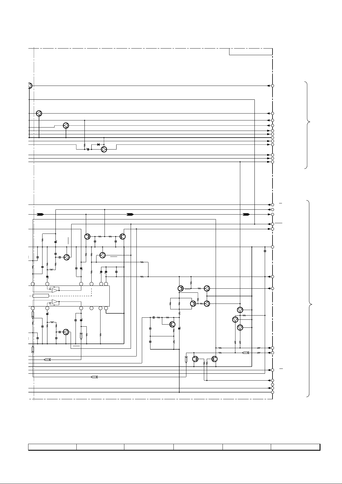
L17
104 M
CHING
0V
12V
4.0V
3
QL18
KRC104 M
2
0V
1
CD-K491W
MAIN PWB-A(2/5)
TA-F/R SPEED
0V
3
12V
QL19
KRC104 M
DRIVER
2
0V
1
+B
0V
3
DL11
0V
1SS133
RL24
3.3K
CL13
3.3/50
1
2
4.1V
0V
3
QL16
KRC107 M
TA-MOT-SW
M-12V
TA-SOL
T2-A-FP
TA-CAM-SW
M-GND
T1-RUN
T2-RUN
T2-B-FP
T1-CrO
2
TA–F/R SPEED
1
2
TA-MOT-SW
M-12V
3
TA-SOL
4
T2-A-FP
5
TA-CAM-SW
6
M-GND
7
T1-RUN
8
T2-RUN
9
T2-B-FP
10
T1-CrO
11
T2 CrO
12
2
2
H:CrO2 L:NORM
P24 1-G
TO MAIN SECTION
3
6.8K
37
K
7
18
V
RK38
CK29
470P
CK31
270P
CK33
22/25
0V
HIGH=HI-SP
CK34
22/25
CK32
270P
6.8K
CK30
RK47
CK10
10K
47/25
CK35
CK37
0.022
0.018
2
KRC104 M
RK39
560
SWITCHING
RK41
82
LK01
1.8mH
0.6V
8
–
56K
+
PLAYBACK AND RECORD
+
/PLAYBACK AMP.
–
56K
17
0.6V
LK02
1.8mH
RK42
RK40
82
560
2
CK38
470P
0.018
CK36
0.022
SWITCHING
QK16
KRC104 M
HI.SP
1
3
QK15
CK39
0.0033
ICK01
AN7345K
CK40
0.0033
3
1
3.0V
HI.SP
0V
CK41
47/25
0.3V
9
16
CK42
47/25
PB.MUTE
MUTING
QK17
2SC2878 A
RK43
0V 0V
10K
CK43
0V
0.022
1
0V
2
RK45 10K
RK49 10K
CK45
22/25
RK50
10K
3.7V
0V
14
15
NOR/HIGH
RIPPLE
ALC
ALC
1110
0V
3.0V
RK46
10K
RK48
10K
CK44
0.022
SWITCHING
QK19
KRC104 M
3
0V0V
CK46
220/10
6.0V
13
VCC
GND
12
0V
RK52
1K
MUTING
QK18
2SC2878 A
HI.SP
0V
CK47
0.022
TA T1/T2 H:T1 L:T2
13
14
PB.MUTE H:ON L:OFF
15
PRE L-CH
16
HI. SP H:LOW L:HIGH
PRE R-CH
CK55
0.022
QK30
KRC104 M
RK73
56K
RK72
56K
17
GND(A)
18
+B
12V(A)
19
20
BIAS H:ON L:OFF
+B
REC L-CH
54
REC R-CH
55
TA R/P H:PB L:REC
23
+B
24
REC MUTE
25
BEAT CANCEL
26
TA PB EQ L:NORM H:CrO2
GND(D)
27
P24 1-H
TO MAIN SECTION
0V
RK57
4.7K
RK58
150(1/2W)
CK62
0.047
(ML)
CK50
0.0082
(P.P)
CK51
0.027
(ML)
KTA1266 GR
RK66
27K
QK28
2SC2236 Y
SWITCHING
QK24
RK60
270
RK67
47K
0V
RK68
4.7
LK04
330µH
11.7V
11.7V
LK03
1mH
RK62
47K
11.7V
0V
RK61
270
0V
0V
CK52
47/16
RK64
4.7K
BIAS
RK63
0V
0V
SWITCHING
QK25
KTA1266 GR
MUTING
QK22
KTC3199 GR
0V
0V
SWITCHING
KRC104 M
23
11.6V
10K
RK65
0V
2
0V
KRC104 M
0.7V
RK54
10K
QK26
1
1
10K
QK27
0V
0.7V
0V
RK53
10K
0V
3
0V
QK29,QK30,
QK40:SWITCHING
QK40
KRC107 M
KRC107 M
RK55
22K
RK56
22K
0V
MUTING
QK21
KTC3199 GR
0V
QK29
11.7V
RK74
68K
3
0V
1
RK81
11.7V
6.8K
2
3
0V
1
11.7V
3
0V
2
0V
1
0V
2
RK75
68K
7
8 9 10 11 12
Figure 27 SCHEMATIC DIAGRAM (6/20)
– 27 –
Page 28

CD-K491W
Q
K
Q
C
C
9
Q
K
A
RP51
1K
RP53
100K
CP58
0.068
QP1
KT
B
C
D
E
F
G
ICR11
GP1F38T
PHOTO DIGITAL
OUTPUT /LED
DIGITAL-OUT
L-CH
INPUT
VIDEO/AUX-2
R-CH
L-CH
INPUT
VIDEO/AUX-1
R-CH
JR11
JR12
LR01
1
2.2µH
2
3
CR02
100/10
CR03
0.001
CR10
0.001
DR11
1SS133
DR12
1SS133
RR15
27K
CR13
390P
CR14
RR16
390P
27K
RR11
27K
CR11
390P
CR12
390P
RR12
27K
TO MAIN SECTION
CR01
0.022
RR17
1.8K
RR18
1.8K
RR13
1.8K
RR14
R-CH
GND(A)
VIDEO-1
P24 6-H
TO CD SERVO PWB
RR01
100
ZDR01
MTZJ3.3B
1.8K
851881841880
L-CH
R-CH
GND(A)
VIDEO-2
P23 11-D
CNS99
DOUT
+4.3V
CNPR11
3
2 1 1
2
QR13
KRA107 M
1
QR12
KRA107 M
3
2
1
QR11
KRA107 M
2
3
1
S.W.
L-CH
REAR
MUTE
MUTE
TO MAIN SECTION
P25 12-B
GND
323130
MUTE
CENTER
3
DOUT
2
CR17
4.7/50
RR21
47K
CR16
4.7/50
RR20
47K
TO DOLBY PWB
P34 1-A
CNSA11
GND
CNPR12
CR15
4.7/50
RR19
47K
CP41
2.2/50
CP42
2.2/50
S.W.MUTE
CENTER MUTE
CP31
CP32
0.001
0.001
RP35
100K
RP33
1K
CP29
2.2/50
CR65
47/25
CR66
47/25
–B
+B
58
AC3-C IN
AC3-SW IN
TO MAIN SECTION
AC3-LS IN
AC3-RS IN
P25 10-G
RP11
100
CP13
0.001
L-CH IN
L-CH
RP15
100K
CP14
0.001
RP16
100K
5554575676
RP36
100K
RP34
1K
CP30
2.2/50
NJM4565M
BUFFER AMP.
CP19
CP15
0.1(ML)
0.1
(ML)
RP17
8.2K
CP17
47P
CP18
47P
RP18
8.2K
CP16
0.1
CP20
(ML)
0.1(ML)
RP12
100
R-CH IN
ICP11
RP19
2.2K
RP20
2.2K
RP52
1K
5
6
2
3
+
–
–
+
RP54
100K
REAR MUTE
+B
8
(1/2)
RP21
100
CP07
100P
CP08
100P
RP22
100
(2/2)
4
–B
CP44
0.001
CP23
10/16
7
RP27
47K
RP28
47K
CP24
10/16
1
KTC3199GR
RP25
1K
RP26
1K
RP32
220
QP14
CP09
CP10
47/25
47/25
+B
CP27
CP28
QP16
KTC31
0.022
0.022
RP31
220
CP37
0.001
CP38
0.001
CP25
0.001
CP26
0.001
KT
H
• NOTES ON SCHEMATIC DIAGRAM can be found on page 16.
1
23456
Figure 28 SCHEMATIC DIAGRAM (7/20)
– 28 –
Page 29

CP27
QP15
KTC3199GR
QP16
KTC3199GR
GR
QP13
KTC3199GR
CP37
0.001
CP38
0.001
CP47
0.001
CP53
0.001
RP47
RP70
5.6K
5.6K
RP48
5.6K
RP62
5.6K
GND(A)
FM SIGNAL
MAIN PWB - A ( 3 / 5 )
OUT6
RELAY4
OUT4
OUT5
GND(A)
RELAY3
+B
CFWP02
13
12
11
10
9
8
7
6
5
4
3
2
1
OUT6
RELAY4
OUT4
GND(M)
OUT5
+12V(M)
GND(A)
FAN SW
RELAY3
VOL SW
PROT
POSISTOR
AMP
CD-K491W
FWP02
1
13
TO SPEAKER
AMP.1 PWB
P38 1-F
CFWX11
+B
CP28
0.022
CP25
CP26
0.022
KTC3199GR
RP31
220
QP11
KTC3199GR
RP29
5.6K
0.001
RP30
5.6K
0.001
QP12
S-MUTE
GND(A)
–B
–B
–15V
S-MUTE
+B
+B
GND(A)
+12V(A)
–15V
+12V(A)
CP57
22/25
RP73
22K
+B
29271918283318
GND(D)
+4.6V(D)
+4.6V(D)
GND(D)
AMP
TO MAIN SECTION
RELAY2
RELAY4
RELAY3
P25 12-B
PROT
VOL SW
H/P SW
POSISTOR
RELAY1
SP LEVEL
FAN CONT
+B
3
+12V(M)
POWER
OUT3
RELAY2
OUT1(L-CH)
RELAY1
GND(A)
FAN CONT
OUT2(R-CH)
SP LEVEL
H/P SW
VOL SW
PROT
POSISTOR
+B
46454443424140393837363534
7
GND(M)
+7.3V(CD)
CD GND(D1)
+B
50
494847
VGND
GND(D3)
+5V(AC3-A)
CD GND(D2)
+B
535251
GND(D4)
+5V(AC3-B)
123
VF1
–VP
QP17
KRC107 M
SWITCHING
3
1
CP91
100/6.3
WTP02
VF2
TO DISPLAY PWB
P36 1-B
FWD02
2
RP91
100
+B
CNPP02
VOLTAGE
REGULATOR
QP91
2SD468 C
+12V(M)
+B
WTP01
CFWP01
OUT3
16
RELAY2
15
OUT1(L-CH)
14
RELAY1
13
GND(A)
12
FAN CONT
11
OUT2(R-CH)
10
SP LEVEL
9
GND(M)
8
H/P SW
7
+12V(M)
6
FAN SW
5
VOL SW
4
PROT
3
POSISTOR
2
AMP
1
CNPP01
1
–15V(A)
2
GND(A)
3
+12V(A)
4
+12V(M)
5
GND(M)
+4.6V(D)
6
7
GND(D)
8
+7.3V(CD)
9
CD GND(D1)
10
CD GND(D2)
11
POWER
1
VGND
+5V(AC32A)
2
GND(D3)
3
GND(D4)
4
1
VF1
2
–VP
3
VF2
FWP01
1
16
TO POWER PWB
P40 1-H
CNS901
TO POWER PWB
P40 6-H
CNS902
TO POWER PWB
P41 8-H
FW901
TO SPEAKER
AMP.2 PWB
P38 1-B
CFWV11
7
8 9 10 11 12
Figure 29 SCHEMATIC DIAGRAM (8/20)
– 29 –
Page 30

CD-K491W
VR CLK
A
B
C
D
E
F
G
MAIN PWB - A ( 4 / 5 )
67 6869707172 73
VR CLK
–B
RZ10
100
CZ04
10/16
BUFFERAMP.
ICZ02, ICZ04, ICZ06:
CLK2
VR LA TCH
VR DATA
DI
CLK
VR DATA
VR LA TCH
–B
CZ28
0.022
CZ25
0.022
–7V
7
+7V
ICZ06
1
NJM4565M
–7V
7
+7V
ICZ04
1
NJM4565M
–7V
7
+B
+7V
NJM4565M
1
CZ70
100P
RZ04
6.8K
DI
A
4
4
4
8
ICZ02
FUNC A
FUNC B
B
+B
CZ27
100/10
CZ26
100/10
(2/2)
8
(2/2)
8
(1/2)
(2/2)
(1/2)
–
+
(1/2)
+– +–
+– +–
–+
6
5
2
3
6
5
2
3
6
5
3
2
L-OUT
54 55
L-OUT
R-OUT
RZ42
680
CZ24(ML)
0.039
RZ36
680
CZ20(ML)
0.033
RZ30
680
CZ16(ML)
0.012
RZ24
680
CZ12(ML)
0.0015
RZ18
680
CZ08
270P
CZ02
1/50
C-IN
SWIN
SRIN
SLIN
R-OUT
58 56 57 76 27
C-IN
SLIN
SRIN
SWIN
GND(D)
D GND
+B
RZ75
10
+B
–B
GND
–7V
CZ22
0.33/50
RZ40
RZ38
330K
1M
RZ32
RZ34
1M
330K
RZ28
RZ26
270K
1M
RZ20
RZ22
1M
120K
RZ16
RZ14
1M
120K
RZ12
1M
RZ08
RZ06
100K
1M
+7V
RZ02
6.8K
+B
PLAYBACK SIGNAL
GND(D)
DZ01,DZ02:1SS133
RZ76
1K
RZ78
+7V
RZ77
1K
42 41 40 39
CLK
DATA
DVDD
OUT3(NC)
OUT2(NC)
OUT4(NC)
1 2 3 4
CZ48
1/50
VEE
14
VCC+7V
S
13
12
TEST1
11
TEST2
F1
10
(ML)
CZ18
0.18
9
F2
(ML)
CZ14
0.27
8
F3
(ML)
ICZ01
CZ10
0.027
LC7522
7
F4
CZ06
0.0047
6
F5
5
F6
4
F7
3
IN2
2
IN1
1
VDD
FM SIGNAL
TO MAIN SECTION P25 8-D
SW OUT
SR OUT
SL OUT
R OUT
L OUT
C OUT
76 57 56 58 55 54
L OUT
R OUT
C OUT
SL OUT
SR OUT
SW OUT
RZ82
10K
RZ79
10K
RZ81
10K
RZ80
10K
CZ55
0.001
CZ54
0.022
DZ02
DZ01
1K
CZ56
1/50
CZ57
1/50
CZ58
1/50
CZ59
SR OUT
SW OUT
1/50
SL OUT
C OUT
38 37 36 35 34 33 32 31 30 29 28 27 26 25
A GND
D GND
LA TCH
RZ84
CZ60
10K
1/50
R OUT
CZ61
RZ83
1/50
L OUT
10K
–B
–7V
AVSS
CZ67
22/16
(NC)CL2
(NC)CL1
ICZ10
M62446FP
6CH ELECTRONIC VOLUME
OUT1(NC)
AVDD
SWIN
6
5
+7V
RZ70
10K
RZ43
1K
15
16
DI
17
CLK
RZ37
18
VSS
1M
19
F1
CZ21
0.33/50
F2
20
(ML)
CZ17
0.18
21
F3
(ML)
CZ13
0.27
22
F4
CZ09
0.027
RZ13
1M
23
F5
CZ05
0.0047
24
F6
RZ11
1M
F7
25
RZ05
1M
IN2
26
27
IN1
GRAPHIC EQUALIZER ELECTRIC VOLUME
NC
28
7
RZ72
10K
RZ31
1M
RZ25
1M
RZ19
1M
GNDS
CZ50
RZ44
8
1/50
RZ95
+B
SRIN
220
1K
RZ39
330K
RZ27
270K
RZ21
120K
+B
CZ01
1/50
+B
RZ33
330K
RZ15
120K
RZ07
100K
RZ01
6.8K
9
+7V
CZ29
0.022
SLIN
GNDR
GNDC
C IN
10
11 12 13 14 15 16 17 18 19
CZ51
1/50
CZ49
1/50
RZ71
10K
RZ69
10K
ZDZ03
MTZJ5R1A
CZ71
1/50
CZ23
5
0.039(ML)
6
RZ41
680
CZ19
3
0.033(ML)
2
RZ35
680
CZ15
5
0.012(ML)
6
RZ29
680
CZ11
3
0.0015(ML)
2
RZ23
680
CZ07
5
270P
6
RZ17
680
NJM4565M
3
2
ICZ03, ICZ05, ICZ07:
BUFFER AMP.
+–
(1/2)
+–
(1/2)
+–
(2/2)
+–
(1/2)
+–
(2/2)
ICZ03
(1/2)
CZ69
100P
R IN
CZ30
100/10
CZ31
8
4
8
4
8
4
RZ03
6.8K
GND
0.022
–7V
–7V
7
1
7
1
7
1
L IN
CZ32
+7V
+7V
+7V
CZ52
100/10
+B
–7V
ZDZ01
MTZJ7.5C
(NC)CR1
BYPASSR
1/50
R IN
L IN
–B
CZ33
0.022
ICZ07
ICZ05
–B
QZ01,QZ02:
VOLTAGE
REGULATOR
RZ85
CZ64
1K
1/50
CZ63
10/50
24 23 22
(NC)CR2
(NC)RTRE
(NC)RBASS3
BYPASSL
LTRE(NC)
LBASS3(NC)
CZ53
1/50
RZ73
10K
RZ74
10K
RZ89
470K
RZ88
470K
RZ87
470K
RZ65
100
NJM4565M
NJM4565M
RZ91
22K
RZ90
RZ09
100
22K
CZ03
10/16
QZ03
KRC107 M
+B
–B
QZ02
QZ01
KTA1271 Y
(NC)RBASS1
(NC)RBASS2
LBASS2(NC)
LBASS1(NC)
21
20
RZ66
100
8
+7V
5
RZ57
1K
RZ54
1K
2
1
1
3
+7V
–15V
SPE-ANA
+12V
77 28 19 18 861887
–15V
+12V
SPE-ANA
–B
RZ86
+B
+B
1K
KTC3203 Y
CZ65
10/50
+B
+B
–B
CZ62
22/16
+B
–B
RZ93
1K
CZ47
10/16
7
RZ61
10K
(1/2)
+
–
6
CZ45
47P
CZ43
10/16
CZ37
0.022
CZ36
47/16
CZ35
0.022
CZ34
10/16
RZ53
1K
2
10
A
3
QZ04
KRC107 M
16
0X1X2X3X0Y
12
RZ45
1K
78
TUN L
LT IN
RT IN
GND(A)
GND(A)
LT IN
RT IN
GND(A)
GND(A)
CZ66
1/50
ZDZ02
MTZJ7.5C
ICZ09
NJM4565M
LT IN
RT IN
GND
BUFFER AMP.
RZ64
RZ63
100K
100K
RZ62
10K
ICZ09
NJM4565M
BUFFER AMP.
RZ59
RZ60
2.7K
2.7K
RZ56
100K
RZ55
100K
CZ41
0.022
CZ40
47/16
CZ39
0.022
CZ38
10/16
9
8
6
B
Vss
INH
15 11
14
RZ47
1K
RZ491KRZ511KRZ461KRZ481KRZ50
84
85 82
15
TAPE L
AUX1 L
AUX2 L
1K
RZ94
CZ46
10/16
(2/2)
–
CZ44
47P
13
X COM
1Y2Y3Y
1 5 2
17
TUN R
TAPE R
1
1K
80 81
RZ67
100
4
–7V
+
32
RZ58
1K
CZ42
10/16
3
Y COM
4
RZ52
1K
AUX1 R
–B
RZ68
100
–B
–7V
–B
7
ICZ08
TC4052BF
DUAL 4CH ANALOG
AUX2 R
MULTIPLEXER
H
• NOTES ON SCHEMATIC DIAGRAM can be found on page 16.
1
23456
Figure 30 SCHEMATIC DIAGRAM (9/20)
– 30 –
TO MAIN SECTION P
25 8-C
Page 31

1K
@
RQ06
1K
@
RQ07
1K
@
RQ08
CD-K491W
0.0027(ML)
0.022(ML)
CQ10 10/50
CQ09 10/50
CQ12 0.22/50
@
330K
RQ21
DQ02
1SS133
CQ23
0.022
(ML)
CQ19
2.2/50
CQ18
2.2/50
1SS133
13
14
15
16
17
18
19
20
21
22
23
24
DQ01
CQ14
CQ15
330
RQ09
47/25
0.022
CQ20
2.2/50
CQ16
2.2/50
CQ17
2.2/50
CQ21
0.47/50
CQ22
0.022(ML)
ZDQ01
MTZJ5.1B
+B
10
11
9
12
AC
AR
MO
BYP
P/S
VDD
RROUT
RLOUT
COUT
FROUT
FLOUT
21
3
QXAC
4
25 26
CQ24
0.0047(ML)
SPRED
ICQ01
QS7777PF
Q-SOUND
DECORDER
QXBC QXCC
5
3
2
1
28 29 30
27
CQ25
0.47/50
(ML)
0.022
CQ26
CQ27 0.022(ML)
MUTE
4
@
CQ11
CQ13
5 6 7 8
4
GND
MSC3
MSC2
MSC1
PSAVE
5
1
214
3
VCC
31
33 34
32
CQ32
CQ31 0.47/50
0.022(ML)
CQ28 0.0047(ML)
2 3
1
CQ07
MSC6
48
0.012(ML)
VREFOUT
VREFIN
47
MSC5
CQ06
46
MSC4
0.001(ML)
45
RRIN
44
RLIN
43
SUBIN
42
CIN
41
FRIN
40
FLIN
4
39
3
38
QXDC
2
37
CQ35
35 36
CQ34
0.47/50
CQ33 0.022(ML)
CQ03
2.2/50
CQ02
2.2/50
0.022
(ML)
CQ08
0.082
(ML)
CQ04
2.2/50
CQ05
2.2/50
CQ01
2.2/50
CQ36
0.022(ML)
1K
@
RQ01
1K
@
RQ02
1K
@
RQ05
1K
@
RQ03
1K
@
RQ04
1K
@
RQ14
1K
@
RQ13
1K
@
RQ15
1K
@
RQ11
+B
1K
@
RQ12
RQ20 100K
RQ19 100K
RQ16 100K
RQ17 100K
RQ18 100K
RQ10
220
+B
47/25
CQ30
CQ29
100/10
(OS-CON)
FM SIGNAL
66
575658
64 65
QS_SPRED
RR_OUT
QS_AC
QS_MO
TO MAIN SECTION
7
54
C_OUT
L_CH_OUT
RL_OUT
P25 12-C
19 18
55
R_CH_OUT
+12V(A)
63 59
62
L_CH_IN
R_CH_IN
GND(AU)
60
C_IN
61
RL_IN
RR_IN
MAIN PWB - A ( 5 / 5 )
8 9 10 11 12
Figure 31 SCHEMATIC DIAGRAM (10/20)
– 31 –
Page 32

CD-K491W
A
KARAOKE PWB-L
BI601
1
1
V.CAN
2
2
OUT(L)
TO MAIN PWB
CNPU02
P25 12 - D
3
3
GND(A)
IN(L)
+B
5
5
+12V(A)
6
6
OUT(R)
IN(R)
CNSU02
948
7
FM SIGNAL
948
7
GND(D)
MIC
VOLTAGE
REGULATOR
Q631
KTC3203 Y
C627
0.022(ML)
C628
15K
R616
R618
15K
10K
2.3V
2.3V
0.0082
23
22
LPF2 IN
DA INT OUT
+B
R669
220
+B
0.082(ML)
C630
0.22(ML)
C629
0.068
(ML)
2.3V
21
DA INT IN
R668
1.2K
6.4V
5.4V
4.7V
+B
0.6V
20
DA CONT
C673
0.022
C632
100/10
4.7V
19
VCC
C672
47/25
R670
220
C677
47/25
ZD631
MTZJ5.6B
R667
100
C674
47/25
C631
0.022
B
C
L-in
R-out
C620
2.2/50
2.3V
28
R LINE OUT
C623
2.2/50
2.3V
27
L LINE IN
C622
R-in
DIGITL
ECHO
VR603
20K(B)
2.2/50
2.3V
26
R LINE IN
C626
0.1/50
R615
C624
0.1/50
2.3V
25
ECHO VOL IN
3.3K
R617
C625
2.3V
24
LPF2 OUT
C619
1.6V
100P
0.5V
31
MIC SW
D601
L-out
1SS133
C621
2.2/50
2.3V
2.3V
29
30
L LINE OUT
MIC ECHO OUT
V.CAN
+B
D
E
C617
R612
0.15/50
2.3V
36
VCFIL
56K
4.7V
35
VALC
R610
C618
1K
0V
34
AUD SW2
R614
0.01(ML)
R611
0V
33
AUD SW1
39K
1K
32
CLOCK
IC601
MIC AMP.
M65845FP
MIC IN
ALC1
MIC1 NF IN
1
2
3
0V
2.3V
2.3V
C605
F
R604
R603
1K
C604
2.2/50
MIC1 OUT
4
2.3V
270P
150K
C633
VR602
MIC2 IN
MIC1 VOL IN
5
6
2.3V
2.3V
C606
0.1/50
2.2/50
20K(B)
MIC2 VOLUME
ALC2
7
0V
R636
C608
MIC2 NF IN
8
2.3V
C609
R605
1K
2.2/50
MIC OUT
9
2.3V
270P
C611
150K
C610
VR601
MIC2 VOL IN
MIC OUT
10
11
2.3V
2.3V
0.1/50
R606 15K
2.2/50
20K(B)
MIC1
VOLUME
LPF1 IN
LPF1 OUT
13
12
2.3V
C612
0.0082
R608 15K
R607 10K
C634
0.082
AD INT IN
AD INT OUT
15
14
2.3V
2.3V
2.3V
R609 33
C613 0.068(ML)
C614
(ML)
AD CONT
16
0.6V
0.22
(ML)
REF
17
2.3V
C615
GND
18
0V
220/10
R619
C616
22K
0.15/50
G
R602
J602
5.6K
MIC2
C602
0.47/50
H
• NOTES ON SCHEMATIC DIAGRAM can be found on page 16.
1
23456
Figure 32 SCHEMATIC DIAGRAM (11/20)
– 32 –
R601
5.6K
C601
0.47/50
J601
MIC1
Page 33

RT03
22
RT10
4.7K
RT08
10K
CT15
0.022
RT04
47
C309
330P
C310
0.001
R311
100K
L311
560µH
Q361
KRC107 M
Q365
KRC107 M
C343
15P (CH)
CT13
3.9P(UJ)
C390
100P
R396
1K
R398 1K
R397
1K
VDT02
KDV147B
C397
0.022
CF352
AM IF
T351
R352
1K
R371 1K
R372 1K
R373 1K
R374 1K
C338
0.001
C301
0.001
C349
1/50
C321
0.0039
D317
1SS135
R326
1K
C380
1/50
R302
82
R390
82K
C383
0.0022
R316
22K
D316
1SS135
LT02
SW2 OSC
T308
MW OSC T306
TT01
T302
T303
SW1 ANT
T304
SW2 ANT
D353
1SS133
X351
456kHz
C365 0.022
C363 0.022
C364 10/16
C355
22P
Q354
KTC3199 GR
MUTING
MUTING
Q353
KTC3199 GR
10K
R365
R367
1K
C375
3.3/50
R368
33K
R357
470K
R356
1K
C368
1/50
R350
2.7K
C367
1/50
C366 0.001
C398
100/10
C399
0.022
270
R353
C354
0.022
C353
0.022
C307
0.047
TC302
C308 (UJ)
8.2P
TC303
Q308
2SC2878 B
Q309
2SC2878 B
R314
3.3K
R312
33K
VD302-B
KV1236Z23F
D309
1SS135
D310
1SS133
D311
1SS135
R315
22K
R313
22K
C311
0.022
D315
1SS135
D314
1SS133
D313
1SS133
D308
1SS135
D307 1SS135
D306
1SS135
D305
1SS135
CT03
4.7P
RT06
10
CT04
0.001
VDT01
KDV147B
1DT01
SS133
ICT01 TA7358AP
CT16
10/16
LT01
CT02
0.01
CT01
18P(CH)
FM BAND PASS
BFT01
D302
1SS133
D301
1SS133
0.047
C305
C304
0.022
C303
0.022
C314
0.022
R317
10K
R330
1K
R325
56K
C320
0.0018
R329
100K
C319
0.022
VD302-A
KV1236Z23F
R328
10K
C318
0.022
R322
5.6K
C316
0.1
R320
10K
R318
1.5K
R324
100K
R319
100K
C331
0.047
VD301-1
KV1236Z23F
C342
0.022
VR351
10K(B)
C350
0.022
IC303
LA1832
FM IF DET./FM MPX./AM IF
C373
0.022
C374
0.022
R361
5.6K
R362
5.6K
C371
1/50
C372
1/50
R359
1.8K
R382
150
R381
10K
R380
1.5K
R379
2.2K
IC302
LC72131
PLL CONTROLLER
X352
4.5MHz
D352 1SS133
R366
10K
D304
1SS133
D303
1SS133
C394
47/16
C393
2.2/50
R321
5.6K
1SS133
D312
C315
0.1
VD301-2
KV1236Z23F
C336
470P
R323
68K
R327
5.6K
Q307
2SC2878 B
TC304
Q306
2SC2878 B
TC305
R384
5.6K
R383
5.6K
L351
100µH
C385
0.01
R393 1K
C370
1/50
L352
100µH
R391
390
R392
390
ZD351
MTZJ4.7B
C396
100/10
C395
0.022
R377
47K
C392
0.001
C387
0.022
R376
1K
R360
4.7K
C391
47/16
Q360
KTA1266 GR
R385
5.6K
ZD352
MTZJ3.9B
R387
22K
D351
1SS133
RT09
820
C381
12P (CH)
C382
15P (CH)
L356
1mH
R395
47K
C386
330P
R341
47K
Q364
KRA107 M
Q362
KRA107 M
Q363
KRA107 M
R342
47K
R343
47K
C312
0.022
C313
0.022
C351
0.022
R351
5.6K
2.06V
0V
0V
0V
0V
0V
0V
0V
0V
0V
12.18V
0V
0V
0V
0V
5.01V
2.07V
2.06V
0V
0.65V
0.65V
11.6V 12.18V
11.37V
0V
0V
0V
0V
2.52V
2.52V
0V
0V
0V
4.82V
5.1V
0.16V
12.1V
3.85V
3.95V
5.1V
2.38V
0V
0V
0V
2.48V
5.11V
0.9V
0.9V
2.1V
0V
5.09V
5.09V
2.84V
5.01V
3.68V
3.85V
3.85V
3.95V
1.18V
1.19V
2.05V
2.29V
2.52V
0V
0.46V
2.2V
2.2V
5.01V
3.48V
C352
10/16
L353
1mH
R358
8.2K
C362
3.3/50
C361
0.022
L357
4.7mH
L358
560µH
C360
0.022
CF302
10.7MHz
FM1F
R310
22K
C335
18P (CH)
R340
220
R339
470
R338
470
C356
0.001
R354
4.7K
C357
2.2/50
R355
3.3K
C358
1/50
RT02
33K
RT01
100K
QT01
2SC535 C
AMP
RT07
680
RT05
47K
CT10
0.022
CT09
0.0047
CT08 0.0047
CT07 0.001
CT06 0.022
1
98
7
6
5
4321321
11
121314151617202122 1819
10
98
7
6
5
4321
11
10
98
7
6
5
432
131415161718192021222324
12
11
10
9
8
7
6
5
4321
CNP303
R363
1.5K
R364
1.5K
CT12
33P
IF IN
STEREO
MO/ST
SW2
AM IN
FM IN
VDD
PD
AIN
CE
DI
CL
DO
FM
MW
SW1
MO/ST
L-CH
OUT
R-CH
OUT
MPX IN
MPX VCO
FM/AM OUT
AM LOW CUT
VSM
AM RF IN
FM AFC
AM OSC IN
AM OSC OUT
FM IF IN
AM IF IN
AM MIX OUT
REG
GND
SD
STEREO
FM DET
VCC
IF OUT
PHASE
PHASE
(FM/AM)
RF
MIX
B.A
OSC
VCC
NC
NC
FM FRONTEND
SW1 OSC
T307
MW ANT
TP 302
SW2+B
SW1+B
MW+B
AOUT
VSS
X IN
X OUT
CT14
22P(CH)
CT11
15P
(CH)
CT05
6.8P
(UJ)
GND(D)
CL
DO
CE
DI
+12V(A)
GND(A)
TUNER MUTE
L-CH
R-CH
SD
+B
+B
FROM MAIN PWB
P24 1-E
CNSF13
fH
fL
fL
fH
fL
fL
fH
fH
+B
3
2
1
+B
FMIF
3
2
1
3
2
1
3
2
1
FM MUTE
LEVEL
MW TRACKING
AMIF
CF351
FMIF
FM
75ohms
SW2
TRACKING
SW1
TRACKING
SW1
TRACKING
SW1 BAND
COVERAGE
MW BAND
COVERAGE
TUNER PWB-E
FM BAND
COVERAGE
FM
OSC
FM SIGNAL MW/SW1/SW2 SIGNAL
SW1
SW2
MW
GND
SO301
ANTENNA
TERMINAL
FILTER
FMRF
FMIF
+B
3
2
1
3
2
1
3
2
1
C334
18P
(UJ)
C330
8.2P
(UJ)
C306
10P (UJ)
7
– 33 –
8 9 10 11 12
Figure 33 SCHEMATIC DIAGRAM (12/20)
CD-K491W
Page 34

CD-K491W
D
0 047
R
R
3
1
J
33V
CD D-IN
+B
BIA11
1
2
3.3V
1
2
LA14
10µH
CB21
0.001
+B
3
LH51
1µH
LH52
1µH
DH51
1SS133
CA28
0.1
CA27
CA25
10/16
RA01
CA21
CA22
RH61
10/16
0.0015
150
DH52
1SS133
CB14
0.001
DB01
1SS133
DB02
CA30
0.1
RA28
RA27
150
+B
CA26
0.1
ICA13
AK4520A
20BIT 2CH A/D
D/A CONVERTER
RA02
22
22
+B
0.0015
2.3V
RA09
330
CA19
0.1
2.3V
RA10
330
CA20
0.1
RH62
150
CH52
220P
CH54
RH64
150
RH63
150
CH61
0.001
DA15
CA32
0.1
1SS133
DA16
DA11
1SS133
DA12
1SS133
150
CA23
CA24 0.1
2.3V
1 2 3 4
4.6V
RA23
330
RA25
10K
7
8
4.7V
+B
RA24
330
RA26
10K
7
8
4.7V
+B
CA18
CH53
22/25
+B
CH55
220P
22/25
+B
1SS133
1SS133
10/16
R-CH
2.3V
VCOM
VREFH
0V
4
0V
CA17
4
0V
10/16
1
2
3
5
CH62
0.022
RH56
AOUTR
VREFL
–
+
–
+
L-CH
2.3V0V3.9V
2.3V
10/16
2.3V
ICH51
NJM2246M
OPE AMP.+ SW
5.1V
4.3V
5.0V
5.0V
2.2K
Vcc
CA34 0.1
CA33 10/16
1 1 2 2 3 3 4
1.7V
RA29
3.9V0V3.3V
PWAD
AOUTL
CMODE
AINL+
AINR–
AINR+
6
5
2.3V
2.3V
2.3V
RA17
10K
6
2.3V
5
2.3V
RA21
10K
RA19
10K
CA15
10/16
RA18
10K
6
2.3V
5
RA22
10K
RA20
10K
CA16
0V
4.5V
11.9V
4.2V
RH65
120
CH60
1000/10
ZDH51
MTZJ9.1B
ICA15
74HCU04F
INVERTER
RA33
RA32
47K
1.7V
47K
2.2K
RA30
+B
0V0V0V0V0V
202122232425262728
VD
DGND
PWDA
AGND
VA
AINL–
8
9
7
0V
3.3V
2.3V
RA07
10K
2.3V
1
CA13
0.1
2.3V
1
CA14
0.1
10/16
8
7
6
4
CH56
47/25
+B
RH66
150
CH59
47P(CH)
19
TST1
DIF0
101112 13 14
+B
RA15
10K
OPE AMP.
RA16
10K
NJM4580M
OPE AMP.
RH53
100
RH67
390
23456
Figure 34 SCHEMATIC DIAGRAM (13/20)
A
TO MAIN PWB
P28 3-C
CNPR12
DVD2 IN
CNSA11
2
1
COAXIAL
JA11
DIGITAL-IN
DVD1 IN
OPTICAL
ICA14
GP1F38 R
TERMINAL
B
C
D
E
JH51
F
VIDE01 IN
VIDEO2 IN
MONITOR OUT
G
H
• NOTES ON SCHEMATIC DIAGRAM can be found on page 16.
1
2.2K
1.6V
8
9
GND
6
5
7
0V
1.7V
18
TST3
TST2
DEM1
DIF1
LRCK
SCLK
3.3V
1.6V
1.6V0V1.0V
RA08
10K
2.3V
2
–
RA13
10K
+
3
2.3V
ICA11
NJM4580M
2.3V
2
–
RA14
10K
+
3
2.3V
ICA12
RH58
CH57
0.022
LH53
QH51
CH58
0.047
KTC3199 GR
RH57
RH68
470
47K
+B
– 34 –
+B
151617
1.6V
MCLK
DEM0
SDTO
SDTI
CA11
22/16
RA11
47K
CA12
22/16
RA12
47K
47K
+B
100µH
+B
+B
2
4.2V
KRC102 S
SWITCHING
CA35 10/16
CA98
10/16
+B
+B
2
4.2V
0V
V1/V2
1
0V
QH52
CA36 0.1
CA97
0.1
+B
QH53
1
KRC102 S
SWITCHING
GND(V)
3
0V
+B
0V
3.4V
3.4V
15161011121314
14
2G
Vcc
B
1G
0V
0V
2.8V
LA17
18µF
3
0V
CB15 0.001
13
A
1C3
0V0V0V
2C3
1C2
1C1
4
5
2.7V
RA92
47K
RA91
47K
CB16
0.001
FM SIGNAL
0V
10
9
1112
2Y
ICA16
2C1
2C2
2C0
74HC153F
INVERTER
GND
1Y
1C0
8
6
7
0V
1.7V0V1.7V
+B
RA54
270
RA55
270
CA37
0.001
CA38
0.1
CA39
0.1
+B
CB20
0.001
CA51
100/10
LA13
0.82µH
LA16
18µH
+B
DGND
SI
PWAD
SS
SO
DGTL2
DGTL1
DEM1
SCK
RESET(ZR)
RA39 1K
DA13
CFWA02
2 3 4
1 1
5
SI
SCK
AD RES
AC3_RES
DEM0
RA35 1K
RA34 1K
RA36 1K
RA37 1K
1SS133
DA14
1SS133
10 11 12 13 14 15 161718
8
9
6
7
SO
SS
DEM0
DEM1
DGTL1
DGTL2
SP CONF
1 20
FWA02
CFWU02
TO MAIN PWB
P25 12-F
CA47
RA49
270
0.001
+B
RA50
1K
RA51
270
RA52
1K
RA53
1K
RA56
270
RA60
10K
+B
+3.3V
+B
MT ZJ8.2A
MT ZJ8.2A
CA49
LA12
ZDA02
ZDA01
18µH
0.1
3.3V
4.0V
1.0V
3.3V
3.3V
1.6V
3.3V
3.3V
1.6V
CA50
100/10
+B
0.1
CA48
81
82
83
84
0V
85
0V
86
0V
87
0V
88
0V
89
0V
90
91
92
93
0V
94
95
96
97
98
0V
99
100
RA40
1K
+B
RA93 680
RA48
270
0V0V0V
VDD
GND
RESET
SDA
VDD
SDE
TCK
SCK
TDI
SI
GND
SCKA
WSA
VDD
SDF
WSB
D17
SCKB
D16
SPFTX/SDG
D15
SS
1 2 3 4
0V
0V
3.8V
VOLTAGE REGULATO
CB13
0.022
–B
RA96
RA95 680
A17
A18
A19
D18
SDC
79
SDB
80
A0
1
GND
2
TMS
INT
VDD
6
5
7
3.3V
RA41
10K
QB01
2SD2012
UN-SWITCHED
3.4V
4.0V
CB12
100/10
680
0V
D19
CLKOUT
DOLBY
AU
D14/RDY
GNDA1A2
10 11
8
9
0V
5.4V
RB12
390
ZDB
MTZ
CA96
47/25
CA95
47/25
GND
CA46
7071727374757677787980
VCCA
A3
RA94 680
A+12V
A-12V
+B
CB22
0.001
AGND
19 20
2 3 4
LTIN
RTIN
A-12V
AGND
VGND
A+12V
GND(D3)
GND(D4)
+5V(AC3_A)
+5V(AC3_A)
+5V(AC3_B)
5
V1/V2
AGND
RS IN(RS-OUT)
8
6
7
R-OUT
LS IN(LS-OUT)
L-OUT
1
CFWU01
TO MAIN PWB
P25 12-E
Page 35

DEM0
DEM0
+B
CA49
0.1
CA48
RA50
3.3V
1K
4.0V
1.0V
RA51
3.3V
270
0V
0V
RA52
1K
0V
0V
0V
0V
RA53
1K
RA56
270
CA37
0.001
CA38
0.1
CA39
0.1
18µH
RA60
10K
+B
+3.3V
LA12
3.3V
1.6V
3.3V
0V
3.3V
1.6V
0V
RA40
1K
CA50
100/10
18µH
RA57 270
+B
20
01
LA16
+B
DGND
ZDA02
MT ZJ8.2A
ZDA01
MT ZJ8.2A
DEM1
+B
RA37 1K
A+12V
CB22
0.001
01112131415161718
DEM1
GND(D3)
GND(D4)
VGND
+5V(AC3_A)
+5V(AC3_A)
CA47
0.001
0V0V0V
0.1
VDD
81
82
RESET
SDA
83
84
VDD
85
SDE
86
TCK
87
SCK
88
TDI
89
SI
90
GND
91
SCKA
92
WSA
93
VDD
SDF
94
WSB
95
D17
96
97
SCKB
D16
98
SPFTX/SDG
99
D15
100
1 2 3 4
+B
RA93 680
RA94 680
+B
AGND
19 20
A+12V
+5V(AC3_B)
RA49
270
RA48
270
A18
A19
GND
SDC
79
SDB
80
A0
1
GND
2
SS
TMS
INT
5
0V
0V
3.8V
RA41
10K
VOLTAGE REGULATOR
UN-SWITCHED
3.4V
4.0V
CB13
0.022
–B
RA96
680
RA95 680
A-12V
2 3 4
1
LTIN
RTIN
A-12V
AGND
1
20
+B
CB27
0.1
RB09
560
CA46
0.047
3.3V
1.7V
0V
0V
0V
1.8V
A17
D18
D19
GND
VCCA
FLTCAP
CLKOUT
DOLBY AC-3/5.1CH MPEG2
AUDIO DECORDER
VDD
D14/RDY
GNDA1A2A3VDD
10 11 1213141516 171819 20 212223 24 26 27 28 29 3025
8
9
6
7
0V
5.4V
RB12
390
3.3V
RB11
390
ZDB11
MTZJ3.9B
3.3V
QB01
2SD2012
CB12
100/10
VDD
GNDA
SCKIN
ICA18
RZ38600
D13/C/D
D12/ERR A4VDD
GPIO5
+B
CB11
47/25
+B
GND
XTI
3.3V
SW-ON/OFF
8
6
7
L-OUT
R-OUT
LS IN(LS-OUT)
SW-CH
C-CH
RS-CH
LS-CH
L-CH
RB07
100K
RB08
100K
R-CH
CFWA01
10
9
C IN(C-OUT)
SW IN(SW-OUT)
10
RB05
100
RB06
100
CA96
47/25
CA95
47/25
5
V1/V2
AGND
RS IN(RS-OUT)
FWA01
0V
0V
3.3V
1.7V
P/M
XTO
VDD
SPFRX
BYPASS
GPIO4
GND A5A6
D11/PP7
0V
QA01~QA03:SWITCHING
-7.8V
RA83
100K
QA02
KRA107 S
-7.8V
7.8V
3
1
0V
QA01
KRC107 S
+B
–B
–B
+B
7.8V
-7.8V
8
4
3
+
0V
1
–
2
RB03
27K
CB05 220P
CB06 220P
RB04 27K
–
6
0V
7
+
5
CB17
0.001
ICA17
TC7WU04U
DUAL2–INPUT NAND GATE
+B
3.3V
1.7V
1.7V
8
6
5
CA52
10/16
3.3V
GPIO0
GPIO1
GPIO2
WR
51
CS
52
GND
29
VDD
30
A7A8D10/PP6A9A10
GPI03
QA03
KRC107 S
3
1
-7.8V
–B
2
1
7.8V
2
7.8V
3
0V
CB04
0.022
CB03
0.022
0V
CB01
0V
100P
RB01
22K
RB02
22K
0V
CB02
100P
0V
ICB01
NJM4580M
OPE AMP.
7
Vcc
1 2 3 4
CA53 0.001
0V
0V
1.7V
1.7V
RA44
270
0V
0V
51
545556575859606162636465666768697071727374757677787980
5253
RD
50
SDD
VDD
GND
A16
49
3.3V
48
D4/PP0
47
D5/PP1
A15
46
3.3V
45
VDD
0V
GND
44
A14
43
D6/PP2
42
D7/PP3
41
A13
40
TOO
39
A12
38
0V
GND
37
0V
SELEX7
36
VDD
35
0V
SO
34
33
D8/PP4
32
D9/PP5
A11
31
CA41
0.1
CA40
0V
0.1
3.3V
MIC/AUX INPUT SELECTOR
-7.8V
+B
100K
+B
RA87 22K
RA85 3.3K
CA93
2.2/50
RA88 22K
-7.8V
7.7V
12
0V
10
7.7V
13
0V
2
RA82
+B
CA54
18P(CH)
XA11
GND
12.288MHz
RA59 1M
CA55
22P(CH)
+B
CA45
0.1
CA44
0.1
CA43
0.001
RA43
10K
RA42
1K
CA42
0.001
+B
ICA22 BU4066BCF
5
3
6
9
2
CA92
0.022
14
7
-7.8V7.8V
CA91
0.022
0V
0V
0V
11
0V
CD-K491W
RA03 22
+B
+5V
RA04 22
CA56 0.047
CA57 10/16
ICA19
AK4321
0V
1
CKS
4.6V
+B
2
DVDD
0V
3
DVSS
XT0
4
2.2V
5
XT1
3.9V
6
PD
1.8V
7
BICK
AOUTL
0V
8
SDATA
AOUTR
1.6V
9
LRCK
0V
10
SMUTE
0V
11
DFS
0V
DEM0
12
20BIT 2CH
D/A CONVERTER
+B
+B
+B
4
8
RA80
100K
0V
+B
0V
2.2V
3.9V
1.6V
0V
1.6V
0V
10
0V
11
12 13
2.3V
+B
D/A CONVERTER
ICA21
NJM4580M
OPE AMP.
0.1V
CA88
2.2/50
RA79
1K
RA05 22
RA06 22
CA71 0.047
CA72 10/16
CKS
1
DVDD
2
DVSS
3
XT0
4
XT1
5
PD
6
BICK
7
SDATA
8
LRCK
9
SMUTE
DFS
DEM0
ICA20
AK4321
20BIT 2CH
7
CA87
-7.8V
0.001
RA78
18K
CA86
0.022
AOUTL
AOUTR
1
(1/2)
1
C-CH
RS-CH
LS-CH
DZF
VREF
AVSS
AVDD
VCOM
DEM1
BVDD
DIF1
DIF0
DZF
VREF
AVSS
AVDD
VCOM
DEM1
BVDD
DIF1
DIF0
2
4
–B
+B
4.6V
TTL
24
23
4.6V
22
0V
21
20
2.3V
19
L-CH
18
R-CH
17
16
CA64
4.6V
15
+B
4.6V
14
0V
13
+B
CA67 10/16
CA68
10/16
+B
CB26
0.001
4.6V
TTL
24
23
22
0V
21
20
2.3V
19
2.3V
18
2.3V
17
16
+B
CA80
15
14
+B
CB18
0.01
CA83
RA75
3
0V
+
5
0V
–
CA84
6
8
7.8V
CA85
0.022
+B
RA89
22K
RA90
22K
DOLBY PWB–G
2.3V
2.3V
10/16
220
RA64
RA68
220
CA73
220/6.3
CA75 0.1
CA76 0.1
C-CH
SW -CH
10/16
RA74
220
2.2/50
1K
47P(CH)
RA76
RA77
2.7K
+B
+B
CA63
RA63
RA67
+B
CA79
RA73
LA18
100K
CA58
220/6.3
10/16
220
220
10/16
220
18µH
+B
CA81
0.015
CA82
0.1
+B
CA74
CA59
0.001
CA60
0.1
CA61
0.1
CA62
100/16
RA61
27K
RA62
27K
CA65
0.015
CA66
0.015
CA69
0.015
CA70
0.015
0.001
RA65
27K
RA66
27K
CA77
RA71
RA72
L-CH
R-CH
100/16
27K
27K
WU02
AIN PWB
5 12-F
CFWU01
TO MAIN PWB
P25 12-E
7
8 9 10 11 12
Figure 35 SCHEMATIC DIAGRAM (14/20)
– 35 –
Page 36

CD-K491W
M
10K
1K
G
B
K
DISPLAY PWB-C1
A
B
C
D
E
HP-LCH
GND(A)
HP-RCH
H/P SW
WTV11
P39 12-D
GND(M)
TO SPEAKER AMP.2 PWB
FWD02
P29 10-G
WTP02
TO MAIN PWB
GND(D)
+4.6V(D)
+12V(M)
COM1
P24 1-A
CNPF01
RESET
TO MAIN PWB
DATA1
STB
SCK1
FM SIGNAL
FWV91
RV91
5
220
RV92
220
1
HEADPHONES PWB-C3
3
VF2
–38(VP)
VF1
1
CNSD01
10
9
8
7
6
5
4
3
2
1
(YELLOW)
LEDD20
KL052UL
(GREEN)
LEDD21
SLR505MC-1
+B
LV91
2.2µH
CV91
RD54
1.2K
RD55
820
100P
CV92
100P
QD07
KRC107 M
2
1
3
2
1
JV91
HEADPHONES
3
R-PLAY
QD08
KRC107 M
REW
FLD01
3
S44
(0V)
P31
NC
S43
(0V)
P32
5
0V0V0V
56
S42
(0V)
(-28V)
P33
6
0V
7
CD05
S41
(-30V)
P34
RD26
0.001
S3S2S1
7
S3S2S1NCNC
S40
(-28V)
81
100
(0V)
P35
8
DISK 1
1K
727374757677787980
P
SC
+
VDD
VDD4
(4.1V)
(0V)
P36
9
DISK 2
RD27
RD60
F1F1NC
2
14
–B
(YELLOW)
F-PLAY
+B
(YELLOW)
STOP
(GREEN)
(YELLOW)
PAUSE
LEDD05
–B
SLR325VR
CD29
1/50
CD30
+B
1/50
LEDD11
SLR325MG
CD18
150P
LEDD14
SLR325MG
LEDD18
SLR325MG
1/50
CD28
+B
+B
FF
SLR325MGX2
LEDD07
LEDD08
SLR325MGX2
LEDD10
SLR325VR
LEDD13
SLR325VR
CD20
150P
CD19
LEDD16
SLR325VR
LEDD17
SLR325VR
CD10
220/6.3
LEDD04
KL052UL
LEDD06
RD53
LEDD09
LEDD12
SLR325MG
150P
150P
CD21
LEDD15
SLR325MG
LEDD19
SLR325MG
LEDD01
KL052UL
LEDD02
KL052UL
LEDD03
SLR505MC
1K
CD11
RD50
RD52
560
2
0.022
RXD01
N64H380A
REMOTE
SENSOR
RD49
1.2K
820
2
RD51
1.2K
2
1
QD05 KRC107 M
3
1
RD57
39
2
RD48
1.2K
2
1
3
QD06
KRC107 M
1 3
QD01
KRC107 M
3
2
QD02
KRC107 M
1
2
3
QD03
KRC107 M
1
3
RD15
RD16
RD17
QD04
KRC107 M
RD03
1K
RD04
RD05@1K
RD06
RD07
RD08
RD09
RD10
RD11
560
RD12
RD13
RD14
@
1K
@
1K
@
1K
@
@
@
@
@
@
@
@
@
1K
1K
560
1K
560
1K
1K
560
1K
(4.0V)
(0V)
FF
(0V)
PAUSE
(4.0V)
(0V)
(0.6V)
(10.8V)
(-6.0V)
(10.8V)
(0V)
VSS
(4.1V)
VDD
(0.6V)
(10.8V)
(9.0V)
(0.4V)
(0V)
DATA1
(0V)
COM1
SCK1
(0V)
(0V)
STROBE
RD19
1K
RD22
1K
+B
DD01
1N4004S
DD02
1SS133
1
3
CD09
150P
1K
RD02
F-PLAY
STOP
81
S46
S47
(0V)
PG1
82
PG2 Q SOUND-G
83
PG3 Q SOUND-R
84
P00 PHANT-G
85
P01 PHANT-R
86
P02 VIRTUAL-G
87
P03 VIRTUAL-R
88
VSS2
89
VDD2
90
P04 NORMAL-G
91
P05 NORMAL-R
92
P06 STEREO-G
93
P07 STEREO-R
94
SO0
95
SI0
96
SCK0
97
SO1
98
SI1
99
100
P17
P16
2 3 4
1
0V
(0.6V)
RD21
1K
RD58
100K
RD01
NC
S45
(0V)
(0V)
P30
R-PLAY
1K
(0V)
REW
RD59
100K
F
RE16
3.9K
F-PLAY
RE29
27K
G
SWD29
BYPASS Q-SOUND
RE39
27K
SWD38
CLEAR
NORMAL
SWD37
SLEEP
RE28
12K
RE38
12K
SWD27 SWD28
PHANTOM
TIMER
RE27
5.6K
RE37
5.6K
SWD26
VIRTUAL
SWD35 SWD36
MEMORY
RE26
3.9K
RE36
3.9K
REC/
PAUSE
SWD34
CLOCK
H
• NOTES ON SCHEMATIC DIAGRAM can be found on page 16.
1
23456
Figure 36 SCHEMATIC DIAGRAM (15/20)
RE15
2.2K
RE25
3.9K
RE35
2.2K
– 36 –
ITEM
HIGH
EDIT
R-PLAY
+B
RE04
1.8K
RE14
1.8K
RE34
1.8K
SWD05 SWD06
MENU
NORMAL
EDIT
SWD23
REV
MODE
RE03
1.2K
RE13
1.2K
RE23
RE33
1.2K
1.2K
STOP
CD
PAUSE
RE02
RE12
RE22
RE32
1K
1K
1K
1K
SWD03 SWD04
X-BASSPRE EQ.
SWD12 SWD13 SWD14 SWD15 SWD16 SWD17
TUNING UP/CUE
SWD30 SWD31 SWD32 SWD33
TUNING DOWN/
REWIND
KEY5
KEY1
RE41
KEY6
RE51
8.2K
8.2K
RE01
8.2K
KEY2
RE11
8.2K
RE21
8.2K
KEY3
RE31
8.2K
KEY4
Page 37

CD-K491W
0
001
RD26
S2
S41
P34
(
30V)
0V
S12
S11
S10
S4
S3
8
9
7
+B
VDD
S4
S3
717273
4
70
S39
S40
VDD4
-
(-28V)
(-30V)
(4.1V)
81
PG0
S9S8S7S6S5
11 12 13 14
10 16 17 18 1915 20 21 23 24 25 26
S12
S11
S10
S9S8S7S6S5
S38
S37
S36
S35
S34
S33
S32
S31
(-21V)
(-30V)
(-30V)
(-30V)
(-30V)
(-30V)
(-30V)
(-28V)
ICD01
IX0234AW
SYSTEM
MICROCOMPUTER
100
SCK1
V
(4.0V)
(0V)
(4.0V)
(4.0V)
(4.0V)
(1.7V)
(0V)
(0V)
(0V)
P35
P37
/RES
INT0 FL-SET
P36
8
9
10 111213 1415161718 19 202122
0V
RESET
DISK 1
DISK 2
DISK 3
RD27
1K
RD29
10K
1K
1K
1K
RD28
RD31
10K
RD60
.
SWD01
VOLUME
JOG SW
P74
P75
VSS1
VSS
XD01
0031
VOL JOG UP
VOL JOG DOWN
RD33
1K
RD32
10K
RD61
CF1
XCIN
1K
CD01
0.022
CD02
100/10
RD62
8.2K
0.001
CD06
(1.9V)
CF2
XCOUT
VDD1
VDD
RD34
820
S14
S13
S14
S13
S30
S29
(-26V)
(-30V)
(0V)
(0.4V)
AN1
AN0
TUN-SET
AUD-SET
RD36 1K
RD35 1K
S19
S23
S22
S21
S20
S18
S17
S16
S15
22 28 29 30 32 33 34 3531 36 37 39 40 41 42
S18
S17
S16
S15
S28
S27
S25
S26
(0V)
(0V)
(0V)
(-28V)
50
S19
(4.0V)
(4.0V)
(0V)
(4.0V)
AN5
AN2
AN3
AN4
23 24 25
KEY4
KEY1
KEY2
KEY3
RD40 1K
RD39 1K
RD38 1K
RD37 1K
S19
S24
(-28V)
(-30V)
S2
32
31
S1
(4.0V)
AN6
26 27
KEY5
KEY6
RD41 1K
RD42 1K
S20
S23
(0V)
(4.0V)
AN7
S21
(-23V)
(-29V)
(0V)
(4.0V)
JOG UP
RD43 1K
S22
S22
S21
(-21V)
(-30V)
(-26V)
(4.0V)
(-29V)
(-29V)
(-29V)
(-29V)
(-29V)
(-29V)
(4.0V)
INT1
INT2
28
JOG DOWN
RD44 1K
27
–B
S23
–29(VP)
51525354555657585960616263646566676869
VP
S20
(-26V)
(-28V)
S18
S17
S16
VDD3
S15
S14
S13
S12
S11
S10
(-29V)
S9
(-29V)
S8
(-29V)
S7
(-29V)
S6
(-29V)
S5
(-29V)
S4
S3
S2
(3.5V)
INT3
S0
29
30
G15
REMOCON
RD45 1K
(-30V)
(-30V)
50
49
48
47
46
45
44
43
42
41
40
39
38
37
36
35
34
33
32
31
S24
S25
S26
S27
VDD
G1
G2
G3
G4
G5
G6
G7
G8
G9
G10
G11
G12
G12
G13
G14
S26
S25
S24
+B
(-29V)
LD01
2.2µH
+B
10K
10K
RD64
RD65
0.001
CD07
SWD02
JOG
JOG PWB-C4
1G
2G
3G
NCNCNC
NCNCNCNCS27
38 44 45 47 48 49 505152 53 54 55
0.001
CD08
8G7G6G5G4G
9G
10G
11G
46
43
DISC 3
DISC 2
DISC 1
QD12
KRC107 M
12G
13G
QD10
KRC107 M
3
1
1
3
1
15G
14G
2
223
QD11
KRC107 M
RD72
820
RD70
820
RD71
820
NCNCF2
F2
56 57
DISC 3
DISC 2
DISC 1
LEDD28
LEDD27
DISC3
LEDD25
DISC2
2 3 4
LEDD26
DISC1
+B
1
LEDD24
LEDD23
+B
WHD01
FWD01
1
LMKD515B
LMKD515B
LMKD515B
LMKD515B
LMKD515B
LMKD515B
LEDD23~LEDD28
VHPLMKD515B-1T
RE42
1K
RE41
SWD39 SWD41 SWD42
8.2K
DVD/VIDEO 1
RE52
1K
SWD48
POWER /
STAND-BY
RE43
1.2K
SWD40 SWD43
DVD/VIDEO 2
SWD49
KARAOKE
TAPE
RE53
1.2K
RE44
1.8K
1/2
RE45
2.2K
TUNER
/BAND
RE57
5.6K
SWD54
OPEN/
CLOSE
CD
RE56
3.9K
SWD53 SWD52 SWD51 SWD50
DISC
SKIP
DISC3
RE55
2.2K
DISC2
RE54
1.8K
DISC1
6
5
6
SWITCH PWB-C2
7
8 9 10 11 12
Figure 37 SCHEMATIC DIAGRAM (16/20)
– 37 –
Page 38

CD-K491W
T
A
TO MAIN PWB
P29 12-D
CFWP01
B
C
D
E
TO MAIN PWB
P29 12-B
CFWP02
F
G
H
FWP01
FWP02
QV13
KTC3199 GR
0V
DV13
0V
0V
QY51
0V
1SS133
4.0V
0V
1
–VCC
1
–VCC
0V
–B
2 3 4
–VCC
KTC3199 GR
–B
2 3 4
–VCC
KTC3199 GR
0V
5
GND
GND
GND
QX15
0V
5
GND
GND
GND
QV18
4.0V
6
4.0V
0V
+B
6
4.0V
0V
+B
7
+VCC
4.0V
+B
7
+VCC
CV29
3300/50
+B
+VCC
CX29
3300/50
CNPX1
+VCC
CV28
47/50
CNPV
QX16
KTC3
0V
CX28
47/50
0V
TO
0V
1K
RV31
DV15
1SS133
1K
RV32
DY11
1SS133
1K
RX32
4.0V
4.0V
DY51
1SS133
1SS133
+B
+B
DX13
1SS133
DX14
1SS133
+B
+B
DV14
CV30
3300/50
–B
1SS133
CX30
3300/50
DX15
–B
0V
0V
4.0V
4.0V
0V
RY17
1K
4.0V
0V
RX31
1K
0V
QX14
0V
RY58
1K
RV27
CV11
CV13
CY13
2.2/50
CV14
2.2/50
CY12
2.2/50
470P
CX13
2.2/50
CX14
2.2/50
CY52
2.2/50
RX13
56K
RX14
56K
RY51
56K
RV17
RV13
RV14
RV18
1K
RY12
RY11
RX15
RX16
RY52
1K
56K
56K
1K
56K
1K
1K
1K
CY55
CY54
100/50
2.2/50
16
1
13
1
OUT3
RELAY2
OUT1(Lch)
RELAY1
GND(A)
FAN CONT
OUT2(Rch)
SP LEVEL
GND(M)
H/P SW
+12V(M)
FAN SW
VOL2SW
PROT
POSISTOR
AMP
OUT6
RELAY4
OUT4
GND(M)
OUT5
+12V(M)
GND(A)
FAN SW
RELAY3
VOL2SW
PROT
POSISTOR
AMP
CFWV11
16
15
14
13
12
11
10
9
8
7
6
5
NC
4
3
2
1
CFWX11
13
12
11
10
9
8
7
6
5
NC
4
3
2
1
CENTER
FR
+B
S.W
+B
SU
CV15
CV16
CV12
2.2/50
CY11
2.2/50
CX11
2.2/50
CX15
470P
CX16
470P
CX12
2.2/50
CY51
2.2/50
470P
470P
CY53
470P
CV17
47P
CY14
47P
CX17
RX21
56K
RX19
RX20
47P
47P
390
390
RV19
RY15
390
390
0V
16
0V
15
CV21
RV23
15P
1K
RV21
56K
QV16
KTC3199 GR
CV19
100/50
RV20
390
CV20
100/50
RV22
56K
RV24
CV22
1K
15P
0V
13
CV18
47P
0V
12
0V
18
0V
17
CY15
RY13
15P
1K
RY14
56K
CY16
100/50
0V
16
0V
15
CX19
RX23
15P
1K
QX18
KTC3199 GR
CX21
100/50
CX22
100/50
RX22
56K
RX24
CX20
1K
15P
0V
13
CX18
47P
0V
12
0V
18
0V
17
CY56
RY53
15P
1K
RY54
56K
RY55
390
ICV01-B
3CH AF
POWER AMP.
STK40727
RV35
2.2K
RV36
22K
RV37
47K
DV21
1SS133
CV27
RV38
10K
1000/6.3
RV63
120K
0V
1
2
14
ICV01-A
3CH AF
POWER AMP.
STK40727
0V
ICV01-C
3CH AF
POWER AMP.
STK40727
ICX01-A
3CH AF
POWER AMP.
STK40727
KTA1268 GR
RX35
2.2K
RX36
22K
0V
0V
RX34
0.8V
0V
15K
(1/2W)
RX37
47K
RX38
10K
DX21
1SS133
RX55
0V
10K
1
2
14
ICX01-B
3CH AF
POWER AMP.
STK40727
ICX01-C
3CH AF
POWER@AMP.
STK40727
RV34
-36V
6
QX17
6
15K
RV33
RX33
120K
-24V
RV71
820
10K
0V
-24V
RX71
820
QV17
7
7
11
36.5V
RV25
100
(1/2W)
CV23
KTA1268 GR
47/50
CV24
47/50
RV26
100(1/2W)
-36.5V
10
11
25V
Fusible
RX25
100(1/2W)
CX23
47/50
CX24
47/50
CX27
1000/6.3
-24.5V
10
5
19
37V
Fusible
-37V
4
RX26
100
(1/2W)
19
-25V
4
CV25
0.022
Fusible
3
CV26
0.022
KTC3199 GR
KTC3199 GR
CY17
0.022
0V
20
KTC3199 GR
CX25
0.022
5
25.8V
Fusible
3
CX26
0.022
CY57
0.022
0V
9
8
QY11
0V
9
0V
8
20
0V
0V
QV14
QX13
10K
RV29
0.2(1W)
RV69
0.2(1W)
RV70
0.2(1W)
RV30
0.2(1W)
RV28
10K
RY18
10K
RY16
0.2(1W)
RY26
0.2(1W)
RX27
10K
RX29
0.2(1W)
RX69
0.2(1W)
RX70
0.2(1W)
RX30
0.2(1W)
RX28
10K
0V
KTC3199 GR
KTC3199 GR
RY57
10K
RY56
0.2(1W)
RY66
0.2(1W)
• NOTES ON SCHEMATIC DIAGRAM can be found on page 16.
1
23456
Figure 38 SCHEMATIC DIAGRAM (17/20)
– 38 –
Page 39

DV15
1SS133
V30
0/50
–B
1
–B
2 3 4
–VCC
–VCC
KTC3199 GR
0V
0V
5
GND
GND
QV18
4.0V
6
GND
4.0V
0V
+B
7
+VCC
CV29
3300/50
+B
+VCC
CV28
47/50
CNPV12
QV19
KTC3199 GR
0V
RV40
56K
TO POWER PWB
P40 5-A
CNS903
RV41
RV42
56K
56K
FM SIGNAL
RY19
56K
0.1(ML)
CY19
CD-K491W
SPEAKER AMP.2 PWB-F2
TMV01
SPEAKER
RLYV11
CV31
0.1(ML)
CV33
0.1(ML)
RV43
4.7(1/2W)
RV44
4.7(1/2W)
CV34
0.1(ML)
CV32
0.1(ML)
CY18
0.1(ML)
RY20
4.7(1/2W)
@
+B
DV17
1SS133
RLYY11
DY12
1SS133
+B
RV62
RELAY2
FAN SW
FAN CONT
3.3K
QY12
KTC3199 GR
RY21
3.3K
SP LEVEL
H/P SW
RELAY1
+B
DV23
22K
RY23
RV54
22K
QV22
KTC3199 GR
0V
0V
0.6V
RV61
47K
0V
0V
0.6V
1SS133
RY22
47K
DV24
1SS133
RV53
DV19
1SS133
27K
RV60
ZDV11
MTZJ5.1B
22K
DV20
DV25
1SS133
1SS133
CV48
10/50
CV37
0.022
CV41
0.022
CV38
0.022
CV42
0.022
RV59
100K
CV39
0.022
CV40
0.022
RV55
RV57
4.7K
RV72
RV58
CV35
0.022
CV36
0.022
47
MTZJ6.2B
0V
22K
CV49
100/50
DV22
1SS133
10K
330(1/2W)
ZDV12
0V
RV52
CV43
0.001
RV56
3.9K
8.8V
QV21
KTC3199 GR
RV51
330(1/2W)
TERMINAL
+
–
+
–
CV44
0.001
+
–
CV45
0.001
CV47
CNPV11
47/25
2
1
9.3V
8.8V
QV20
0V
KTA1270 Y
WTV11
5
4
3
2
1
CNSV11
2
1
FAN MOTOR
HP-L CH
GND(A)
HP-R CH
GND(M)
H/P SW
SP2
FRONT-L
8 OHMS
SP1
FRONT-R
8 OHMS
SP3
CENTER
8 OHMS
M
M901
TO HEADPHONE PWB
P36 1-A
FWV91
DX15
1SS133
CX30
00/50
–B
1
–VCC
KTC3199 GR
0V
–B
2 3 4
GND
–VCC
GND
QX15
5
GND
4.0V
0V
+B
6
4.0V
+B
7
+VCC
CX29
3300/50
+VCC
QX16
KTC3199 GR
0V
0V
CX28
47/50
CNPX12
TO POWER PWB
RX40
56K
P40 4-A
CNS904
RX41
RX42
56K
56K
FM SIGNAL
RX43
(1/2W)
RX44
(1/2W)
RY59
56K
CY58
0.1(ML)
RY60
4.7(1/2W)
TMX11
SPEAKER
RLYX11
CX31
0.1(ML)
CX33
0.1(ML)
4.7
4.7
CX34
0.1(ML)
CX32
0.1(ML)
CY59
0.1(ML)
+B
DX16
1SS133
RLYY51
RY61
RX53
22K
22K
DY52
1SS133
RELAY3
RELAY4
FAN SW
+B
RX54
QX20
KTC3199 GR
0V
RX51
3.3K
QY52
KTC3199 GR
0V
RY62
3.3K
22K
RY63
0V
0.6V
0V
0.6V
47K
RX52
27K
RX50
47K
DX17
1SS133
TERMINAL
+
–
+
–
+
–
SP5
SURROUND-L
8 OHMS
SP4
SURROUND-R
8 OHMS
SP6
SUB WOOFER
8 OHMS
SPEAKER AMP.1 PWB-F1
7
8 9 10 11 12
Figure 39 SCHEMATIC DIAGRAM (18/20)
– 39 –
Page 40

CD-K491W
9
G
TO SPEAKER
P39 7-H
CNPX12
A
CNS904
BI904
–VCC
123
123
–B
–VCC
GND
+VCC
GND
GND
4567
4567
+B
+VCC
TO SPEAKER
P39 7-D
CNPV12
–VCC
–VCC
GND
123
123
–B
GND
+VCC
GND
4567
4567
+B
+VCC
BI903
CNS903
B
–B
Q913
R901
2SB1375
C920
47/25
R902
1K
R918
100
47(1W)
–B
C902
C901
47/25
0.022
VOLTAGE
REGULATOR
Q902
C
+B
+4.6V(D)
+B
GND(D)
+12V(M)
VOLTAGE
REGULATOR
Q903
2SD468 C
C906
0.022
R905
22(1/4W)
Fusible
R906
100
C905
47/25
R904
1.5K
ZD902
MTZJ5.6A
2SD2012
C904
47/25
R903
47
VOLTAGE
REGULATOR
Q901
KTC3199 GR
C903
47/25
R917
4.7K
1
23
ZD901
MTZJ13A
GND
R921
100(1W)
Q914
+B
–B
KRC107 M
–B
D991
KBU1003
+B
–B
Q905,Q906:VOLTAGE REGULATOR
Q906
C909
0.022
ZD904
MTZJ8.2C
2SD2012
R911
560
Q908,Q909:
VOLTAGE REGULATOR
Q905
KTC3199 GR
R910
150
C908
47/25
D904
1N4004S
R909
1K
Q904
KRA107 M
SWITCHING
1
23
C907
R908
33K
F999
T500mA L 250V
220/25
+B
R907
560
ZD903
MTZJ13C
C919
4700/25
Q910,Q911:VOLTAGE RE
Q911
+B
+5V(AC3)
+B
2SD2012
D906
1SS133
C915
0.022
CD GND(D)
KTC31
R914
47
C914
100/25
Q9
1
Q907
KRA102 M
SWITCHING
+12V(A)
+7.3V(CD)
CD GND(D)
GND(M)
C911
0.022
D901
1SS133
Q909
2SD2012
D905
1SS133
Q908
KTC3199 GR
R912
47
C910
47/25
D
E
+B
2
3
+B
F
1234567891011
G
1234567891011
BI901
CNS901
43
43
BI902
2
1
2
1
CNS902
GND(A)
–12V(A)
+12V(A)
GND(M)
+12V(M)
+4.6V(D)
TO MAIN PWB
P29 12-E
CNPP01
GND(D)
+7.3V(CD)
POWER
CD GND(D1)
CD GND(D2)
H
• NOTES ON SCHEMATIC DIAGRAM can be found on page 16.
1
23456
Figure 40 SCHEMATIC DIAGRAM (19/20)
– 40 –
VGND
GND(D4)
GND(D3)
+5V(AC32A)
TO MAIN PWB
P29 12-F
CNPP02
Page 41

C954
0.22(ML)
C956
0.22(ML)
F995
T8A L 250V
F996
T8A L 250V
POWER PWB - D
T991
POWER TRANSFORMER
CD-K491W
–B
VOLTAGE REGULATOR
Q911
2SD2012
Q910
KTC3199 GR
R913
R914
906
SS133
D(D)
C914
100/25
560
47
ZD905
MTZJ6.8C
C913
3300/25
+B
R954
220
F991
T.F.
T2.5A L 250V
SW991
VOLTAGE
SELECTOR
F992
T2.5A L 250V
230-240V
220V
127V
110V
F990
T5A
L 250V
AC POWER
SUPPLY CORD
AC 110/127/220/
230-240V 50/60HZ
(242)
D992~D995
2A02
D995
D992
+B
D993
D994
C964
D996
D997
47/50
C965
100/35
ZD952
MTZJ6.8C
D999
D998
+B
–B
–38V
R955
12K
R953
220
D996~D999
1N4004S
C957
0.047
(ML)
C958
0.047
(ML)
C963
47/50
R956
100
R957
VOLTAGE
REGULATOR
Q951
KTA1266 GR
2.2K
C961
220/50
ZD951
C966
0.047(ML)
C967
0.047(ML)
D951
MTZJ33C
C962
47/63
D954
1N4004S
1N4004S
C960
D952
1N4004S
D953
1N4004S
F997
T2.5A
L 250V
220/50
C959
F998
T1.6A
L 250V
220/50
1 3
VF1
VF2
–VP
TO MAIN PWB
P29 12-F
WTP01
FW901
2
7
8 9 10 11 12
Figure 41 SCHEMATIC DIAGRAM (20/20)
– 41 –
Page 42

CD-K491W
RZ77
RZ73
F
P
A
B
C
SWF02
SELECTOR
D
E
L-CH
JR12
INPUT
VIDEO/AUX-2
R-CH
F
G
L-CH
JR11
INPUT
VIDEO/AUX-1
R-CH
DIGITAL OUT
SPAN
10/100
FM/MW
9/50
MAIN PWB-A
RZ45
RZ48
RZ47
RZ46
1
DR12
ICZ08
RR15
RR11
DR11
LR01
CNPR12
CQ09
CR01
12
CZ42
CZ43
CQ05
CR02
RZ53
916
8
RZ55
CQ03
CQ06
CQ07
CQ08
ZDR01
CNPR11
RZ51
CR13
RR17
CR14
RR18
CR11
RR13
CR12
RR14
CR10
ICR11
RZ52
RR16
RR12
3
2
1
RZ49
RZ50
3
2
1
CZ41
ICZ09
RZ57
CQ02
QZ04
CZ35
RZ56
4
CZ40
58
CZ45
CQ04
CQ10
RR01
123
RZ90
CZ38
RZ58
RZ59
CQ01
RZ91
CZ39
CZ44
RZ61
CQ14
CQ11
CQ12
CR03
TO SPEAKER AMP.1 PWB
P50 2-A
CFWX11
TO TUNER PWB
P48 1-B
CNP303
1123456789
RDBKBKBKBKBKBKBKBKBKBK
1
BIF13
CZ58
RZ82
CZ56
QP11
RZ80
CZ06
CZ08
RZ18
RZ16
RZ14
14
CZ70
RZ04
21
2728
RZ02
CZ66
ZDZ02
CNPP01
123
4567891011
58
RZ06
RZ05
ICZ02
CZ01
11
10
RZ81
CZ57
42
CZ62
1
CZ50
CZ48
RZ70
RQ15
RQ13
RQ14
CZ22
CZ14
RZ28
CZ16
RZ30
RZ26
5
8
CZ26
ICZ04
14
RZ08
RZ20
RZ24
CZ12
RZ22
RZ12
CZ10
9876543
ICZ01
RZ11
242526
CNPU02
9 8 7 6 5 4 3 2 1
RZ86
CP31
CP18
RP18
CP10
58
ICP11
CP19
CP17
CZ11
RZ21
CZ15
RZ27
CZ13
RQ17
QZ01
RP91
BCE
FWP02
13
QP15
RP48
CP38
B
C
QP14
E
RP22
RP20
CP08
14
CP09
RP15
RP17
RP19
CZ63
CZ09
RZ23
RZ19
ICZ03 ICZ05 ICZ07
4
58
RZ15
RZ25
RZ29
RQ18
BCE
DQ02
DQ01
CNPP02
1234
RP30
E
C
B
RZ07
CZ07
CZ64
QP16
B
C
E
CP26
CP24
CP27
CP07
RZ03
1
B
C
E
QP12
CP23
RP21
CZ69
RZ17
CP47
RP47
QP13
RP29
B
C
E
RP26
RP25
CZ04
RZ13
RQ11
RQ12
ZDZ01
RQ08
RQ07
RQ06
123
WTP01
123
CP37
CZ05
WTP02
CNSF13
B
C
E
RP28
RP27
CZ02
RZ01
QZ02
BCE
CP25
CZ03
RZ85
1
CP53
RP52
RP54
CQ25
RQ03
CQ23
CQ20
1412108642
RP70
RP62
RQ05
97531
108642
CQ30
RQ01
CQ28
CQ27
CQ17
CP42
CFWU01
RQ10
RQ20
RQ21
191715131197531
201816
CP44
RP53
CP58
CP41
RP34
CP30
CP29
RP32
RP12
RP31
RP11
RZ33
CZ31
CZ30
581458
CZ23
CR65
RZ39
CZ32
CZ33
RQ19
RP51
RP36
CP16
CZ19
RP33
CP28
CP13
CP32
RP35
RP16
CZ17
RZ41
CZ21
CZ65
QP91
RZ35
14
CP20
CP14
CP15
RZ31
RZ37
RQ09
CP91
3
2
QR13
1
3
2
QR11
1
QR12
123
QZ03
3
2
1
RZ54
RZ65
CZ34
RZ68
RZ62
RZ60
CZ46
CZ47
1
CZ36
CQ36
48
1
CZ37
CQ35
ICQ01
40
45
5
12 13
CQ15
CQ13
CQ34
3637
35
10
15
ZDQ01
30
20
RQ16
RZ63
CQ33
RZ64
RZ94
CR66
RQ04
RZ93
RZ67
RZ66
RQ02
CQ29
CQ32
CQ31
CQ26
25
24
CQ24
CQ21
CQ22
CQ18
CQ16
CQ19
CFWU02
TO SPEAKER AM
CFWV11
BK
RG01
CZ59
RZ10
RZ42
RZ36
RZ71
CZ24
CZ20
1413121110
151617181920212223
ZDZ03
RZ79
25303540
RZ88
RZ09
RZ40
58
ICZ06
RZ34
RZ84
CZ28
CZ29
1
QG04
BCE
CZ60
22
21
RZ69
RZ87
CZ27
CZ25
CZ71
BIF11
11
ICZ10
5101520
CZ49 CZ51 CZ52 CZ53
RZ72
RZ89
RZ38
14
RZ32
CZ18
P50 5-A
RZ83
DZ02
RZ74
RZ75
RK73
3
DZ01
RZ4
RZ4
RZ95
CZ61
CZ55
RZ76
20
CNSA11
TO DOLBY PWB
P46 2-E
H
1
CNS99
TO CD SERVO PWB
P47 10-H
23456
FWA02
CFWA02
TO DOLBY PWB
P46 3-A
Figure 42 WIRING SIDE OF P.W.BOARD (1/10)
1
10
CFWA01
TO DOLBY PWB
P46 5-A
1
FWA01
CNS902
TO POWER PWB
P51 9-H
FWD02
TO DISPLAY
FW901
TO POWER PWB
P51 7-D
PWB
P44 1-F
CNS901
TO POWER PWB
P51 7-F
CNSU02
FROM KARAOKE
PWB
P49 7-A
123
CNS
CNP11
TO CD SERVO PWB
P42 9-H
– 42 –
Page 43

RZ36
RZ42
RZ10
TO SPEAKER AMP.2 PWB
P50 5-A
CFWV11
1
QG04
BCE
RG01
RZ79
RZ83
RZ84
CZ60
22
DZ02
2530
Z10
10 15 20
21
49 CZ51 CZ52 CZ53
RZ71
RZ69
RZ74
RZ75
RZ87
RZ88
RZ09
CZ24
CZ28
RZ40
CZ27
5
ICZ06
4
RZ34
CZ25
CZ20
8
1413
CZ29
1516
ZDZ03
CZ71
3 2 1
BIF11
1
3
123
02
AOKE
-A
CNP11
TO CD SERVO PWB
P42 9-H
DZ01
RZ76
RK73
RZ43
RZ44
RZ95
CNSF11
CZ61
CZ55
RZ77
FWP01
CZ54
CZ67
RZ73
RZ78
RK72
16
CFWP02
13 11 9 7 5 3 1
12 10 8 6 4 2
16 14 12 10 8 6 4 2
15 13 11 9 7 5 3 1
CFWP01
CG8
RR21
CR17
CR16
RR20
CG04
DG04
3
RG36
2
1
RG37
QG01
DG05
QG92
1
ECB
2
QP17
3
RG95
RK54
123
CK35
RK56
CK55
QK21
1
2
QK40
3
1
2
QK29
3
RK74
RG05
RG06
CG02
CG03
RG94
QG03
RG31
RG35
B
B
QG02
C
C
E
RG39
RG34
RG32
RG29
RG30
CG01
RG96
RG06
RG07
RG08
14
BKBKBKBKBKBKBKBKBKBKBKBKBK
14 13 12 11 10
987654321
TO CD SERVO PWB
CK37
B
C
E
RK55
RK75
CP57
RF71
RF75
RF78
RG23
ZDF01
RG33
DG02
BIF12
CNP12
P47 11-G
QK18
RK41
RK81
RF67
RF68
RF69
RF70
RF74
DG03
RK48
RK53
3
2
1
RG24
QK15
RK69
LG01
QK22
CK44
RK43
QK30
CR15
RP73
RF73
RF81
RF84
E
C
B
CK10
RF82
RF83
E
C
B
RR19
RF85
RH11
RF76
RF77
RF80
CG56
RK57
RK47
QK17
RG11
RF65
RF87
CK60
CK36
321
321
QK19
RK58
CK43
B
C
E
LK01
CH28
RH40
RH12
ICH11
RF66
RF86
RF88
1
RD
CNSF12
CK38
RK49
RF63
DG07
80
81
RK39
CK29
RH17
RF64
RF91
QK27
CK46
RK34
RK33
CH30
3
QK26
QK14
2
3
123
1
2
1
RK28
RK42
RK46
CK42
LK02
QK16
CK34
CK30
RK40
CK45
RK50
CK47
RK52
101112
CK31
CK33
RK37
CK41
CK39
RK31
1
2
3
RK27
CK23
QK13
RK35
DH11
RH15
RH16
RH14
CH13
RH13
CH10
RH24
CH29
RF51
RF54
RF61
RF58
RF59
RF55
RF62
RF79
RF92
RF53
RF60
DG08
55
60
65
70
75
ICF01
85
90
95
5
CG57
100
1
RF98
RF99
RF95
RF97
RG56
RF94
RF93
RF96
RG22
RG19
RG04
WTL11
RL20 RL24
FWM01
TO TAPE MECHANISM PWB
P49 9-D
RK65
CK40
16151413
10
RK63
RK36
RK38
CH15
RH35
DH12
RF52
RK62
RK32
CK32
18
17
ICK01
CK27
RK45
CH25
RF50
RF49
5051
45
15
RF01
CK24
CK26
19
CK28
RH22
RF47
40
20
RF02
RK60
RK61
QK25
RK64
RK25
CH26
E
C
B
RK30
RH21
35
25
QK24
BCE
RK26
RK29
RK23
RH36
CH17
CH18
RF48
RF11
RK13
CK22
CK21
CK25
RG26
RF46
RG55
RF12
RG15
RK24
RH37
31
30
12345678910111213
CK09
RF43
RF44
RG16
QK09
CK19
DH15
CH16
RF29
RF13
RF03
CK20
2423222120
1123445567889
RF30
DL12
CK52
E
C
B
RK22
CK14
CK15
RH39
RH20
RF42
XF01
RF04
CK13
RF32
RF31
RK21
RF25
RF14
CL13
CH27
CH21
DH17
RF40
CL12
RK05
CK16
CK12
CK11
RK19
RH30
RF41
RK67
LK03
QK05
RK02
CK17
DH18
RF39
RF05
DL11
CK18
CH22
RH29
RG25
RF38
CG05CG06
B
C
E
QL15
B
C
E
RK20
RK11
CK05
QK07
RK07
RK17
3
2
1
QK28
E
C
B
RK03
E
C
B
DH13
RF36
RF37
QL16
RL18
RK09
CK02
CH23
RH27
DH16
RG17
RF28
RF27
RF26
RF24
RL17
CK51
B
C
E
RK01
RF35
3
2
1
RK66
QK03
CK07
CNPK01
RH32
RH31
RH26
DH20
RG20
RF34
QL19
LK04
RK68
CK62
RK04
B
C
E
RK12
RK18
123
DH14
CH20
DH19
RG21
RF33
RL16
RL19
B
C
E
QL14
QK04
QK08
CH19
QL18
CK50
B
C
E
RK89
ECB
CH24
RG38
RF23
RF22
RF21
RF20
RF19
RF10
RF09
RF08
RF07
RF06
3
2
1
3
2
1
RL15
RK06
CK06
CK08
RH34
RH25
RL14
1 2 3 4 5 6 7
RK08
CK01
RL13
QK06
QK10
QL13
3
2
1
RK90
CNPK02
3
2
1
QL17
B
C
E
3
2
1
QL12
RK15
RK10
RL11
1
3
5
7
9
RL12
QK11
2
4
6
8
10
B
C
E
QL11
RK14
CNPF01
CNSK02
TO TAPE
MECHANISM
TAPE2 HEAD
P49 11-H
CNSK01
TO TAPE
MECHANISM
TAPE1 HEAD
P49 9-H
CD-K491W
CNSD01
TO DISPLAY PWB
P44 2-F
7
8 9 10 11 12
Figure 43 WIRING SIDE OF P.W.BOARD (2/10)
– 43 –
Page 44

CD-K491W
LEDD03
FF
SWD26
VIRTUAL
FWD02
CV92
RE02
RE03
RD13
DD02
RE25
RD33
RD32
RD58
RE56
LV91
RV91
RV92
RE12
RE27
CD20
CD19
RE23
RE04
RE14
RE13
RE22
RE15
RD01
RD02
RD10
RD09
RD08
RD07
RD06
RD05
RD04
RD03
RE57
RE26
RE16
CV91
CNSD01
RD11
FWV91
1
LELEDD09
LEDD07
LEDD06
LEDD11
LEDD13
LEDD12
LEDD05
LEDD10
F
RD49
1
2
65798
10 1211 13 1514 16 1817 19 2120 22 2423 25 2726 28 3029
LED
SWD54
OPEN/
CLOSE
SWD53
DISC
SKIP
SWD17
F-PLAY
SWD05
MENU
SWD06
ITEM
LEDD01
F-PLAY
LEDD02
STOP
SWD13
STOP
SWD27
PHANTOM
RD
SWD16
REC/PAUSE
SWD23
Q-SOUND
SWD04
PRE EQ
RD52
RD53
QD06
QD05
RD51
321
321
321
321
321
321
1
3
2
QD04
QD03
RD50
QD02
QD01
CD29
CD28
CD30
RD48
RD15
RD16
RD17
RD19
RD31
RD59
CD21
CD18
DD01
SWD01
VOLUME
JOG
CD05
CD06
CD09
CD11
RD39
RD57
RE21
RD61
RD60
SWD03
X-BASS
LD01
RXD01
REMOTE
SENSOR
CD10
ICD0
1
1
2
3
4
5
6 7 8
9
10
1
5
1
51
55
60
65
70
75
80
81
85
90
95
100
SWD02
JOG
5
JOG PW
HEADPHONES
PWB-C3
CNPF01
FROM MAIN PWB
P43 12-G
SWD15
HIGH EDIT
WTV11
JV91
HEADPHONS
FROM SPEAKER
AMP.2 PWB
P50 4-A
WTP02
TO MAIN PWB
P42 5-H
SWD14
NORMAL EDIT
SWD12
TUNING UP/CUE
A
B
C
D
E
F
G
H
1
23456
Figure 44 WIRING SIDE OF P.W.BOARD (3/10)
– 44 –
Page 45

CD-K491W
DISPLAY PWB-C1
FLD01
21
22 2423 25 2726 28 3029 31 3332 34 3635 37 3938 40 4241 43 4544 46 4847 49 5150 525653
51
50
55
45
60
65
81
RD13
75
85
70
90
95
100
LEDD10
SWD27
PHANTOM
SWD02
JOG
ICD01
80
1
JOG PWB-C4
40
35
31
30
25
20
15
10
5
1
LEDD08LEDD09 LEDD15
RD12
RD14
SWD28
NORMAL
LEDD04
PAUSE
LEDD20
R-PLAY
LEDD16
RE28
SWD33
R-PLAY
RD34
XD01
CD01
CD02
LEDD14 LEDD19 LEDD18
SWD29
BYPASS
SWD32
REVERSE
MODE
SWD31
CD PAUSE
RE33
RE32
SWD30
TUNING DOWN/
REWING
CD07
RE34
RE29
CD08
QD07
RD54
LEDD17
REW
LEDD21
3
2
1
RD21
RD55
RD22
3
2
1
QD08
SWD43
CD
57
SWD42
TUNER
BAND
SWD41
TAPE1/2
SWD39
DVD/
VIDEO1
SWD40
DVD/
VIDEO2
RD29
RD26
SWD37
SLEEP
RE39
SWD38
CLEAR
RD27
RE35
RD28
RE38
RD62
SWD34
CLOCK
SWD36
TIMER
RE37
RE36
SWD35
MEMORY
RD36
RD35
RD43
RD42
RD41
RE44
RD45
RD44
RE43
RE45
RE42
QD11
1
2
3
SWD48
POWER
STAND-BY
RD40
RD38
1
2
3
RE31
QD10
RE51
RD37
RD71
RD70
RE41
RD64
QD12
1
2
3
RE11
RD65
RE01
RD72
WHD01
1
6
RE53
RE52
SWD49
KARAOKE
RE55
LEDD25
LEDD26
SWD51
D1SC2
RE54
LEDD23
LEDD24
SWD50
DISC1
1
FWD01
LEDD28
LEDD27
SWD52
DISC3
SWITCH PWB-C2
7
8 9 10 11 12
Figure 45 WIRING SIDE OF P.W.BOARD (4/10)
– 45 –
Page 46

CD-K491W
DOLBY PWB- G (TOP VIEW)
120
FWA02
CFWU02
TO MAIN PWB
A
CB16
E
CA27
CB12
ICA14
1
C
B
QB01
CA52
23
CB11
LA16
CA33
ZDB11
CB14
WH
20
19
18
17
LA12
16
DA13
DA14
CB20
CB15
14
12
10
8
CFWA02
6
4
2
15
13
11
CA50
9
7
5
3
1
CA51
CA35
LA13
LA14
B
C
D
P42 3-H
RB09
1
2
BK
LA11
XA11
BIA11
DA16
CA57
CA72
DA12
DA11
DA15
CA98
ZDA01
ZDA02
CA23
LA17
CA68
CA67
CB21
CA25
DB01
DB02
CA73
CA77
CA58
CA62
LA18
CA96
CH53
CA95
CA79
CA80
CA63
CA64
CA16
CA18
CH55
LH51 LH52
CFWU01
TO MAIN PWB
P42 4-H
CA83
CH56 LH53
CA88
CA15
CA93
CA17
1
CH60
CA11
FWA01
10
CB17
10
9
8
7
6
5
4
3
CFWA01
2
1
CA12
B
C
E
QH51
ZDH51
DH52
DH51
DVD1
DIGITAL IN
WH
12
CNPR12
TO MAIN PWB
P42 2-H
CNSA11
DVD2 IN
JA11
DIGITAL 2
COAXIAL
VIDEO 1
IN
VIDEO 2
IN
VIDEO
OUT
JH51
VIDEO
IN/OUT
BK
E
RA82
QA03
CA91
CB05
RB05
RA11
4
1
RH56
7
814
CB04
RH58
CA92
RB01
RH53
CH57
1
RA80
8
ICA21
RA79
CB03
ICB01
RB02
RA19
CA13
ICH51
8
5
CH62
1
ICA22
F
QH52
RH57
G
RH68
RH65
RH66
CH59
CH58
CH61
RB08
RH67
RA85
RA87
RA89
CB01
RB03
RB07
RA12
CA87
5
8
RB06
CH54
CA86
CA19
RH64
RA83
4
5
RA78
RA88
RA90
CB02
RB04
4
QA02
RA77
CA84
CB06
RA25
1
4
RH63
CA65
CA66
QA01
CA85
CA81
RA76
RA72
CA82
RA61
RA75
RA17
RA09
85
ICA11
1
RA15
RA13
RA62
RA21
RH62
RA71
RA23
RA73
RA74
RA63
RA64
CA21
RH61
ICA12
RA20
CA14
CH52
RA18
RA26
CA20
CA70
QH53
RA14
CA69
RA24
RA10
85
14
CA74
CA75
CA76
CA59
CA60
CA61
RA16
RA67
RA22
RA68
RA66
RA65
CA22
24
20
15
13
CB18
24
20
15
13
CA24
CB26
1
5
10
ICA20
12
RA03
RA04
1
5
CB27
10
ICA19
12
1
CA97
CA26
RA05
RA06
CA71
CA56
RA07
RA51
5
RA50
10
ICA13
RA02
RA28
RA08
RA40
RA41
CA37
CA38
CA39
1
RA60
RA57
100
RA56
95
RA55
RA54
90
RA53
RA52
85
81
80
14
RA49
RA48
15202528
CA47
CA48
CA49
CA30
RA01
RA27
RA30
17
RA29
ICA15
14 8
CA32
RA32
RA93
RB11
RA94
RA95
RA96
5 10152025
ICA18
75
ICA17
148
5
CA46
CA53
CA54
RA59
1
CA34
ICA16
16
RA33
RB12
55606570
CA55
35
40
45
RA44
CB13
CB22
CA40
CA41
CA42
30
31
RA42
50
51
RA43
CA43
CA44
CA45
RA34
RA39
RA36
RA35
RA92
RA91
RA37
8
CA36
9
CA28
H
DOLBY PWB-G (BOTTOM VIEW)
1
23456
Figure 46 WIRING SIDE OF P.W.BOARD (5/10)
– 46 –
Page 47

SENSOR PWB-J
SW3
DISC NUMBER
21
SW1
OPEN/CLOSE
CNS5
21
SW2
MECHA UP
M3
T/T UP/
DOWN LOADING
OR
WH
10
987654321
CNS10
1
GY
-
BIM5
GY
WHBRWH
CD-K491W
SOLENOID
SOLM2
CD MOTOR PWB-K
1
2
3
4
5
6
RD
WH
GY
WH
GY
WH
1
2
3
4
5
6
-
1
2
3
4
CNP3A
5
6
CNS3BCNS3A
+
PICKUP UNIT(306)
6
RD
GY
WH
CNS1A
CNS1B
1
BK
2
WH
3
PK
4
YL
5
BL
1
2
3
4
5
6
7
8
WH
GY
WH
GY
WH
WH
RD
GY
BL
1
PK
2
WH
GY
3
YL
4
BK
5
1
2
3
4
5
6
7
8
CNS2BCNS2A
10
7
M2
SLED MOTOR
+
SW4
PICK UP IN
SPINDLE MOTOR
6421
5398
+
-
M1
CD SERVO PWB-B
M901
FAN MOTOR
CNSV11
RD
2
BR
1
CNPV11
TO SPEAKER
AMP.2 PWB
P50 6-A
C35
1
2
3
4
5
6
R48
C36
CNP10
36
1
2
3
4
5
6
7
8
9
10
CNP3
20
25
30
35
R82
R85
R37
8
7
6
5
4
CNP2
3
2
1
IC3
R12
15
10
IC81
C7
5
1
8
3
6
5
4
7
2
9
C8
R11
C6
R13
R16
R20
1819
1
C54
C4
R8
C5
R10
R14
C9
R21
R19
R22
R25
C14
R27
C16
R28
C81
D91
R83
C82
CNSF11
TO MAIN PWB
P42 6-H
R9
R15
C10
R18
C11
R30
R31
Q91
E
C
B
Q93
CNP11
32
CNP1
R17
C12
3
2
1
1
C85
C31
Q1
R2
C18
Q51
C17
R80
R29
16
17
C13
R26
D2
321
BCE
C3
R1
C15
C2
C1
64
1
5
10
IC1
15
20
12
25
30
35
32
C21
C20
R33
C19
R34
D3
D4
R66
R81
R64
C52
BI99
1
WH
RD
RD
WH
1
R46
60
40
33
R32
Q52
BCE
BK
BK
32
55
45
R88
R89
R90
ZD61
3
CNS99
50
C51
R36
R35
49
48
C34
C33
1
2
3
4
5
R23
R24
R87
R86
C32
L61
11
D1
C30
C57
C28
R45
C25
R40
C29
R44
C22
16 49
17
C50
R54
14 1312 11 10
R41
C26
C27
R42
R39
C23
R38
R43
R50
C24
C56
1
64
5
10
15
IC2
20
25
30
35
33
32
C43
C83
98
7654321
CNSF12
TO MAIN PWB
P43 8-H
R51
C39
C40
C46
R93
C47
C48
C38
R47
C37
R63
R61
R62
48
C53
C44
C49
R57
C45
XL1
C42
C41
R59
R58
R52
R53
R60
60
55
50
45
40
R55
D81
D82
CNP12
• The numbers 1 to 12 are waveform numbers shown in page 52.
7
8 9 10 11 12
Figure 47 WIRING SIDE OF P.W.BOARD (6/10)
– 47 –
CNPR11
TO MAIN PWB
P42 2-H
Page 48

CD-K491W
1 2 3
3 2 1
E C B
321
321
321
321
ECB
ECB
ECB
ECB
ECB
BCE
B C E
1 2 3
123
R321
R302
2345 1
789
6
12
12
131415
11
171819
10
2 3 4 5
1
7 8 96
2 3 4 5
1
7
8 9
6
1110
16
222324
21 20
13 14 15 17 18 1916
2221
20
1 2 3 4 5 6 7 8 9 10 11
FM MUTE
LEVEL
TUNER PWB-E
P42 5-A
CNP303
C383
FROM MAIN PWB
C382
C387
C380
R376
R360
R397
R398
RT09
QT01
CT16
CT15
CT11
CT02
CT01
BFT01
CT08
RT02
R310
D305
D301
D309
D311
D303
D307
C331
R319
D312
T306
C334
C335
TC304
TC305
T307
R325
L353
C349
T308
Q307
Q308
T302
D308
R320
R318
L311
D304
D302
D306
CT09
CT03
CT05
CT10
CT06
C304
C305
C330
C338
C306
C309
C314
R317
R314
R313
C307
C313
C321
C320
R342
R326
R330
R329
VR351
R343
R315
R322
R328
C316
C318
Q306
R327
D313
D317
D315
D314
D310
C319
C336
R323
R324
C315
D316
C310
C311
C303
CT04
RT01
RT08
RT04
RT10
VDT01
VDT02
CT07
LT02
LT01
CT14
CT12
C301
RT05
RT07
RT03
TT01
Q309
R312
R316
T304
T303
TC302
TC303
C308
C312
R311
CT13
DT01
RT06
ICT01
Q362
Q363
Q364
IC302
C391
Q361
R390
R377
R367
R361
R365
R366
R362
R350
R356
R351 R352
C342
R357
C374
C372
C371
C373
C368
C353
C354
C356
C355
R395
C381
C392
C393
C390
C385
C386
C394
C397
C367
C363
C365
C361
C350
C360
R341
C362
C343
R358
C364
Q353
Q354
L352
R374
R385
R384
R371
R381
R380
R379
R396
R338
R339
R340
L351
R387
R382
ZD352
ZD351
D351
D352
R373
R372
R392
R359
R354
C396
C375
C395
C370
C358
D353
R368
R355
C357
C366
R353
L358
L356
CF302
CF351
C352
C351
C399
Q360
C398
CF352
X352
T351
L357
Q365
X351
IC303
R363
R364
R393
R383
R391
VD301-1
VD302-B
VD302-A
VD301-2
CNSF13
FM
75Ohms
GND
SW1
SW2
MW
SO301
ANTENNA
TERMINAL
A
B
C
D
E
F
G
H
1
23456
Figure 48 WIRING SIDE OF P.W.BOARD (710)
– 48 –
Page 49

CD-K491W
TO MAIN PWB
CNPU02
P42 6-H
CNSU02
9
8
7
6
5
4
3
2
1
GY
WH
GY
WH
GY
WH
GY
WH
RD
R667
R668
ZD631
Q631
E
C
B
R670
C672
C673
C677
9
1
R669
C674
VR603
DIGITAL
ECHO
BI601
R611
R612
R604
C626
R610
C627
C618
R603
C605
C622
C623
C621
C617
C619
R614
C608
C604
C606
C633
VR602
MIC2
VOLUME
C620
36
1
C609
R605
R636
MIC LEVEL
C624
R616
R617
20253035
IC601
51015
C612
R607
R606
VR601
MIC1
VOLUME
19
18
R608
C625
C634
R615
C610
C628
C631
C613
R618
R609
C611
C629
C615
C616
C632
D601
C602
C601
C614
C630
R602
J602
MIC2
KARAOKE PWB-L
R619
R601
J601
MIC1
MIC
TAPE MECHANISM PWB-H
SWM4
REC RVS
2
SOLENOID
SOLM1
TAPE MECHANISM ASSEMBLY
FWM1
PHM1
1
4
3
TAPE 1
PLAYBACK HEAD
PK
WH
131312 11 10
BK
GY
BK
PK
WH
213
TO MAIN PWB
P39 12-C
CNPK01
TO MAIN PWB
P39 10-H
WTL11
987654321
FWM1
RECORD/PLAYBACK/ERASE HEAD
HEAD PWB-M
6
CNSK01
YL
BL
WH
GY
1
BI 102
PKWHBK
SWM3
REC FWD
SWM6
CAM
TAPE 2
1
GY
4
FLEXIBLE PWB
CNSK02
WH
BK
PK
BL
BK
YL
WH
MM1
TAPE MOTOR
L
H
FWM2
VRM1
TAPE
1
RM1
1
2
3
4
5
6
7
TO MAIN PWB
P39 12-B
CNPK02
SPEED
CNPM2
SWM5
F. A. S
7
8 9 10 11 12
Figure 49 WIRING SIDE OF P.W.BOARD (8/10)
– 49 –
Page 50

CD-K491W
TO HEADPHONES PWB
P44 2-F
FWV91
FWP01
TO MAIN PWB
P43 7-A
CFWP01
16
1
TO FAN MOTOR
P47 8-G
CNSV11
A
RY20
CY19
WTV11
1 2 3 4 5
QV19
B
C
E
7 6 5 4 3 2 1
CV28
RV40
CV31
RV43
CV33
RV41
RV51
RV52
RY19
RLYV11
CY18
RY23
E
C
B
RV42
DV17
RV53
RV44
CV37
RV61
QV18
CNPV12
CV30
E C B
B
C
E
QY12
CV34
CV35
CV29
CV32
RY22
QV22
DV19
CV39
DY12
RV38
CV41
CV43
RV60
CV45
DV15
CFWV11
DV24
RV54
CV38
10
12
14
16
2
4
6
8
DV23
CV36
1
3
5
7
9
11
13
15
CY11
CV12
RV21
RV23
RV33
CV21
DV21
CV46
CV44
CV27
RV37
RV31
ZDV11
CV11
CY15
RY13
CV14
RV63
DV13
B
C
E
RV59
RY14
CV16
RV71
RV29
RV69
DV20
RV13
CV25
RY21
RV62
RV58
CV15
RV34
QV13
QV16
RV24
RV70
CV40
CV42
RY17
RY26
RY16
RV14
CV24
RV30
RV36
1 2
CNPV11
CV47
E
CV48
C
QV20
B
DV25
RY12
RY18
CY13
RV57
RV56
RV72
CY17
ICV01
20
19
18
17
16
15
14
13
12
11
10
ZDV12
QV21
E
RV55
C
B
DY11
9
8
7
6
5
4
3
2
1
CV49
DV22
QY11
B
C
E
CY12
CV13
RY11
CY16
RY15
CY14
CV19
RV19
RV17
CV17
CV20
RV20
CV18
RV18
CV22
CV23
RV22
RV25
RV26
RV32
QV14
ECB
RV28
ECB
CV26
RV27
DV14
ECB
QV17
RV35
CX34
CX30
RX50
FWP02
CX29
RX54
13
QX20
ECB
RX53
TO MAIN PWB
P42 4-A
CFWP02
CFWX11
DX17
RX52
RY62
RY63
DY52
SPEAKER AMP.1 PWB-F1
1
RX51
1
2
3
4
5
6
7
8
9
10
11
12
13
E C B
QY52
RX21
RX34
RX55
DX21
RX38
RX23
CX27
RX29
RX69
CX19
RX31
CX12
RX33
DX13
RX37
RY66
RY56
RX70
RY58
CY56
RY53
RY54
RX71
RX30
CX14
CX16
C
RX27
B
E
CX15
RX13
RX24 RX14
B C E
CX25
CY51
CX11
CX24
QX13
QX18
CX22
RX32
CX21
RX22
CX20
RX36
CX13
DY51
CY52
RY51
CY54
RX19
RX20
B C E
B C E
RX35
QY51
RX15
CX23
RX25
QX14
B
C
E
RY55
CY55
CX17
RX26
RX28
CX26
DX14
CX18
RX16
QX17
RY57
CY53
RY52
ICX01
TO POWER PWB
CY57
20
19
18
17
16
15
14
13
12
11
10
9
8
7
6
5
4
3
2
1
CNS903
P51 12-E
RLYY11
TO POWER PWB
P51 12-F
CNS904
2
5 6 7
1
3
4
CX28
RLYY51
E C B
B C E
RY60
RX41
RX43
RX42
RY59
CY58
CY59
CX33
CNPX12
DX15
CX31
RX44
CX32
DX16
RLYX11
RY61
B
C
QX15
QX16
RX40
D
E
F
TMX11
SPEAKER
G
TERMINAL
SP6
SUB-WOOFER
8 OHMS
SP5
SURROUND-L
8 OHMS
SP4
SURROUND-R
8 OHMS
SP3
CENTER
8 OHMS
SP2
FRONT-L
8 OHMS
SPEAKER AMP.2 PWB-F2
TMV01
SPEAKER
SP1
FRONT-R
8 OHMS
TERMINAL
H
1
23456
Figure 50 WIRING SIDE OF P.W.BOARD (9/10)
– 50 –
Page 51

CD-K491W
AC POWER SUPPLY CORD
AC 110V/127/220/230–240
50/60Hz
F998
T1.6A L 250V
(285)
(285)
T991
POWER TRANSFORMER
F990
T5A L 250V
SW991
F991
T2.5A L 250V
VOLTAGE
SELECTOR
230–240V110V
220V127V
F992
T2.5A L 250V
POWER PWB-D
T.F.
T991
POWER TRANSFORMER
P42 5-H
WTP01
TO MAIN PWB
P42 5-H
TO MAIN PWB
CNPP01
7
CNS901
WH
WH
WH
WH
WH
WH
WH
WH
WH
WH
WH
RD
1234567891011
D952
D951
C959
ZD951
C961
D904
R913
D905
C910
ZD904
P42 4-H
TO MAIN PWB
D994
C958
C960
ECB
ECB
D995
R912
Q908
D993
F999
R911
C907
F997
T2.5A L 250V
D992
C957
C919
T500mA L 250V
ECB
ECB
R907
Q901
C904
ZD903
C903
Q902
R903
R902
F996
T8A L 250V
C909
D901
123
Q904
R909
R908
R921
321
ECB
ECB
C956
Q906
R910
C908
Q907
C954
Q905
ZD901
Q913
C920
F995
T8A L 250V
1
BI903
D991
7
1
BI904
7
R917
E
R901
C901
C902
1
23
Q914
CB
R918
11
1
R906
C905
R954
R904
1
R953
BI901
R905
BCE
Q951
ZD952
C966
ZD902
Q903
C906
FW901
BCE
D999
1
WHWHWH
CNS902
C915
432
C965
D998
D953
D954
R955
D996
D997
D906
BI902
R957
R956
C964
C962
C967
ECB
ECB
4
ZD905
RD
1
C963
C913
Q911Q909
R914
Q910
C911
C914
CNPP02
8 9 10 11 12
Figure 51 WIRING SIDE OF P.W.BOARD (10/10)
– 51 –
CNS903
RD
WH
WH
WH
WH
WH
WH
RD
WH
WH
WH
WH
WH
WH
7 6 5 4 3 2 1 7 6 5 4 3 2 1
CNS904
P50 4-B
CNPV12
TO SPEAKER AMP.2 PWB
P50 1-A
CNPX12
TO SPEAKER AMP.1 PWB
Page 52

CD-K491W
5ms
0.50 V
1
IC1 20 F.E
5ms
5.0 V
2
IC1 54 DRF
WAVEFORMS OF CD CIRCUIT
STOP PLAY
FOCUS SERCH
0.5ms
6
10.0 V
JP+
0.5ms
7
10.0 V
JP-
0.5ms
8
3
1
0.50 V
JP
0.5ms
9
1.00 V
TE
0.5ms
3
1.00 V
HF
0.5ms
4
5.0 V
HFL
0.5ms
5
5.0 V
TES
0.5ms
1.00 V
3
HF
0.5ms
4
5.0 V
HFL
0.5ms
5
5.0 V
TES
50ms
6
10.0 V
JP+
50ms
7
10.0 V
JP-
50ms
8
0.50 V
JP
50ms
9
1.00 V
TE
CUE
1
2
3
REVIEW
1
2
3
CUE
10
11
10
11
12
20ms
1.00 V
SPO
20ms
2.00 V
CLV+
50ms
1.00 V
SPO
50ms
2.00 V
CLV+
5s
100mV
SLD
PLAY
NORMAL DISC
TN0=01
PLAY
TCD-712 (140mm)
TN0=01
PLAY
TCD-712
0.5ms
10.0 V
6
JP+
0.5ms
10.0 V
7
JP-
0.5ms
0.50 V
8
JP
0.5ms
9
1.00 V
TE
50ms
10.0 V
6
JP+
50ms
10.0 V
7
JP50ms
8
0.50 V
JP
50ms
9
1.00 V
TE
REVIEW
12
0.5s
100mV
SLD
1
1
– 52 –
Page 53

CD-K491W
TROUBLESHOOTING
When the CD does not function
When the CD section does not operate When the objective lens of the optical pickup is dirty,this section may not operate.Clean
the objective lens,and check the playback operation.When this section does not operate even after the above step is taken,check
the following items.
Remove the cabinet and follow the troubleshooting instructions.
"Track skipping and/or no TOC(Table Of Contents) may be caused by build up of dust other foreign matter on the laser pickup lens.
Before attempting any adjustment make certain that the lens is clean. If not, clean it as mentioned below."
Turn the power off.
Gently clean the lens with a lens cleaning tissue and a small amount of isopropyl alcohol.
Do not touch the lens with the bare hand.
• When the turntable fails to stop.
5V
Is from 5 V till 2.5V down pulse (approx. 300 ms)
2.5V
0V
input into the ICF01 pin 84 when the turntable is rotating?
Yes
Is there following voltage input on the ICF01 pin 84 in the
specific state?
When the CD mechanism is moved up: 0V
In other states: 4.3V
No
No
Check the SW3 and the wiring from the ICF01 pin 84 to the
SW3.
Check the MECHA UP SW and the wiring from the ICF01 pin
85 to the MECHA UP SW.
Yes
Check IC2 pin26 Q91 and Q93 and the periphery.
Yes
ICF01 defective.
• When turntable fails to move.
Is there following voltage input on the ICF01 pin 85 in the
specific state?
When the CD mechanism is moved up: 0V
In other states: 4.3V
Yes
Is L output from the IC2 pin 26 during SEC when the disc skip
switch is pressed?
Yes
No
No
Check the MECHA UP SW and the wiring from the ICF01 pin
85 to the MECHA UP SW.
Check the wiring of IC2 pin 26 and Q93 pin 2.
OK
IC2 defective.
Is 4V output from the Q91 emitter during operation stated
above?
Yes
Check turntable motor and turntable mechanism.
No
– 53 –
Check Q91, Q93 and the periphery.
Page 54

CD-K491W
• When the CD tray fails to open or close.
Is there following voltage input in specific state of ICF01 pin 86?
Open state: 0V
Close state: 0V
Intermediate state between open state and close state: 4.3V
Yes
Is H output to IC2 pin 24 or 25 for 7 seconds when the OPEN/
CLOSE key is pressed?IC81 is defective. Replace it.
Yes
Is 4V output between IC81 pins 3 and 7 during operation
stated above?
Yes
Check the loading motor (M1) and the loading mechanism.
• The CD function will not work.
The CD operating keys don't work.
No
No
No
Check the OPEN CLOSE SW and the wiring from the ICF01
pin 86 to the OPEN CLOSE SW.
Check the wiring of the IC2 pins 24 and 25, IC81 pins 1 and 3.
OK
IC2 defective.
Check the periphery of IC81.
OK
IC81 defective.
Yes
Check the CD, DSP, power supply, and 16.93 MHz clock, and
reset terminal.
Yes
Check the waveform of SCK, SO (DATA) and SI (COMM).
Yes
See if the pick-up is the in PICKUP IN SW position.
Yes
If the items mentioned above are OK, check the main
microcomputer ICF01.
• The CD operating keys work.
Check the Focus - HF system.
Playback can be performed without a disc.
Yes
Does the pick-up move up and down twice?
No
0.5s
0.50 V
IC1 16 FD
0.5s
0.50 V
IC1 7 TE
Yes
Focus search OK
Figure 54
Focus search is
performed two
times when play
operation is done
without disc.
1
2
Does the output waveform of IC1(16)(FD) match that shown in
Fig. 54?
No
Check the IC1(50)(CLK) line, 4MHz.
Check the microcomputer data on pins (51)(CL), (52)(DAT)
and (53)CE.
Yes
Check the area around IC3-CNP2.
– 54 –
Page 55

• Playback can only be performed when a disc is
loaded.
CD-K491W
Is the Focus servo active? (Can you hear it working?)
Yes
Does the DRF signal change from "L" to "H"?
Yes
Is HF waveform normal (see the Fig.55-1, 2)?
Yes
Check the tracking system.
HF
1.0V/DIV
0.5µsec/DIV(DC)
(When playing
back the disc)
Figure 55-1
• Check the tracking system.
No
No
No
0.5s
1.00 V
IC1 16 FD
0.5s
10.0 V
IC2 13 CLV+
0.5s
10.0 V
IC1 54 DRF
0.5s
2.00 V
IC1 7 TE
Check the laser diode driver.
Check the area around IC1(16) - (21) (focus servo circuit).
If the disc is not turning, the DRF
should not change to "H".
Level is abnormal.
Waveform is unstable.
Yes
Yes
Yes
Figure 55-2
Check the spin system.
Check the periphery of
IC1 pins 41 and 42.
Check the spin system.
Waveform in case of
normal play-back
2
1
3
4
Check waveform of IC1 pin 7 (TE).
The waveform shown in
Fig.55-3 appears, and nodisc state appears soon.
Play is possible in
TEST mode.
Data cannot be read.
5ms
1.00 V
IC1 7 TE
5 ms
5.0 V
IC1 54 DRF
Yes
Although IL is possible,
Yes
play is impossible.
Tracking servo is
inoperative.
Yes
Check the VCO-PLL system.
Yes
Yes
Check the periphery of IC 1
pin 8 to pin 15, and IC 5 to
CNP2.
Normal jump is impeded,
and the program top
cannot be reached.
4
3
Yes
Check the periphery
of IC 1 pin 14.
Figure 55-3
– 55 –
Page 56

CD-K491W
• Checking the spin system.
Play operation is performed without disc.
Yes
The turntable rotates a little.
No
The turntable fails to rotate or rotates at high speed.
• Checking the VCO-PLL system
Play operation is performed when disc exits.
Yes
Although HF waveform is normal, TOC data cannot be read.
Stop --> Play
As VCO frequency is locked at
0.5s
1.00 V
IC2 3 PDO
0.5s
1.00 V
IC2 16 FD
4.32 M Hz, voltage
of PDO rises and
stabilizes.
2
Yes
Yes
Yes
The spin driver circuit is normal.
Check the periphery of IC1 pins 23 to 27, pin 39, and pin 40, IC2
pin 12 and pin 13, IC5 to CNP3.
Check PDO waveform (Fig. 56).
Abnormal
Check the IC1 pins 43 and 44, IC2 pins 3, 5, 7, 10, and 11.
3
Figure 56
• Although HF waveform is normal and the time
indication is normal, no sound is emitted.
Check IC 2 pin 48 (EFLG).
Yes
Check IC2 pins 37, 40.
Abnomal
Check IC 401 and POWER AMP IC 801.
No
Usually, the number of pulses of flawless disc is 100 pulses/sec
or less.
– 56 –
Page 57

CD-K491W
FUNCTION TABLE OF IC
IC2 VHiLC78622K-1: Servo/Signal Control (LC78622K) (1/2)
Pin No.
1 DEFI Input Input terminal of defect detection signal (DEF). (Connected to OV when not used.)
2 TAI Input For PLL Input terminal for test. Pull-down resistor is integrated. Surely connected to 0V.
3 PDO Output Output terminal of phase comparison for external VCO control.
4 VVSS — Ground terminal for integrated VCO. Surely connected to 0V.
5 ISET Input Resistance connection terminal for current adjustment of PDO output.
6 VVDD — Power terminal for integrated VCO.
7 FR Input VCO frequency range adjustment.
8 VSS — Ground terminal of digital system. Surely connected to 0V.
9 EFMO Output For slice level control EFM signal output terminal.
10 EFMIN Input EFM signal input terminal.
11 TEST2 Input Input terminal for test. Pull-down resistor is integrated. Surely connected to 0V.
12 CLV+ Outout Output for disk motor control. 3 values can be output with the commands.
13 CLV- Output Output for disk motor control. 3 values can be output with the commands.
14 V/P Output Monitor output terminal for automatic switch of rough servo/phase control.
15 HLF Intput Input terminal of track detection signal. Schmit input.
16 TES Input Input terminal of tracking error signal. Schmit input.
17 TOFF Output Tracking OFF output terminal.
18 TGL Output Output terminal for switch of tracking gain "L" increases the gain.
19 JP+ Output Output for track jump control. 3 values can be output with the commands.
20 JP- Output Output for track jump control. 3 values can be output with the commands.
21* PCK Output Clock monitor terminal for EFM data replay. 4,3218MHz as the phase clock.
22* FSEQ Output Output terminal synchronous signal detection. "H" is output when synchronous signal detected
23 VDD — Power terminal of digital system.
24 CONT1 Input/Output General purpose input/output terminal 1
25 CONT2 Input/Output General purpose input/output terminal 2
26 CONT3 Input/Output General purpose input/output terminal 3
27 CONT4 Input/Output General purpose input/output terminal 4
28* CONT5 Input/Output General purpose input/output terminal 5
29* EMPH Output Difference monitor terminal At "H", deemphasis disk is being replayed.
30* C2F Output C2 flag output terminal.
31 DOUT Output Output terminal of digital OUTPUT. (EIAJ format)
32* TEST3 Input Input terminal for test. Pull-down resistor is integrated. Surely connected to 0V.
33 TEST4 Input Input terminal for test. Pull-down resistor is integrated. Surely connected to 0V.
34 N.C. — Terminal not used. Open during operation.
35* MUTEL Output L channel 1 bit DAC Mute output terminal for L channel.
36 LVDD — Power terminal for L channel.
37* LCHO Output L channel output terminal.
38 LVSS — Ground terminal for L channel Surely connected to 0V.
39 RVSS — R channel 1 bit DAC Ground terminal for R channel Surely connected to 0V.
40* RCH0 Output R channel output terminal.
41 RVDD — Power terminal for R channel.
42* MUTER Output Mute output terminal for R channel.
43 XVDD — Power terminal for quartz oscillation.
44 XOUT Output Ground terminal of 16.9344 MHz quartz oscillator.
45 XIN Input Ground terminal of 16.9344 MHz quartz oscillator.
46 XVSS — Ground terminal for quartz oscillation. Surely connected to 0V.
47* SBSY Output Output terminal of synchronous signal of subcode block.
48* EFLG Output Correction monitor terminal of C1, C2, single and double.
Input/Output
"H" for rough servo, and "L" for phase servo.
by EFM signal matches synchronous signal internally generated.
FunctionTerminal Name
Controlled with serial data command
from micro computer.
When not used, set it as the input terminal and
open it by connecting to 0V, or set it as the output
terminal and open it.
In this unit, the terminal with asterisk mark (*) is (open) terminal which is not connected to the outside.
– 57 –
Page 58

CD-K491W
IC2 VHiLC78622K-1: Servo/Signal Control (LC78622K) (2/2)
Pin No.
Input/Output
49* PW Output Output terminal of subcodes P, A, R, S, T, U and W.
50* SFSY Output Output terminal of synchronous signal of subcode frame. It drops when subcode stands by.
51 SBCK Input Clock input terminal to read subcode. Schmit input (Connected to 0V when not used.)
52* FSX Output Output terminal of synchronous signal of 7.35kHz divided from quartz oscillation.
53 WRQ Output Output terminal to stand by output of subcode Q.
54 RWC Input Input terminal of read/write. Schmit input.
55 SQOUT Output Output terminal of subcode Q.
56 COIN Input Command input terminal from microcomputer.
57 CQCK Input Clock input terminal to fetch command input, or pick up subcode from SQOUT. Schmit input
58 RES Input Reset input terminal of LC78622. When turning on power, set it at "L".
59* TEST11 Output Output terminal for test. Used in the open state ("L" output as ordinary).
60* 16M Output Output terminal of 16.9344Hz.
61 4.2M Output Output terminal of 4.2336MHz.
62 TEST5 Input Input terminal for test Pull-down resistor is integrated. Surely connected to 0V.
63 CS Input Chip selection input terminal. Pull-down resistor is integrated.
Connected to 0when not controlled.
64 TEST1 Input Input terminal for test Pull-down resistor is integrated. Surely connected to 0V.
Note: The same potential must be supplied to the power terminals (VDD, VVDD, LVDD, RVDD, XVDD).
FunctionTerminal Name
In this unit, the terminal with asterisk mark (*) is (open) terminal which is not connected to the outside.
DEFI
EFMIN
FSEQ
CLV+
CLV-
V/P
PW
SBCK
SBSY
SFSY
CS
WRQ
SQOUT
CQCK
COIN
RWC
EFMO
Slice level
control
Sync detection
EFM demodulation
CLV
Digital servo
Subcode division
QCRC
µCOM
Interface
Servo commander
VVDDVVss
VCO colck oscillation
clock control
General-use port
PDO
I SET
FR
PCK
TAI
TSTI1
2K x 8bit
Flag processing of C1/C2
error detection and correction
XTAL system timing
TEST1
TEST2
RAM
generator
TEST3
TEST4
TEST5
VDDVss
RAM address
generator
Interpolation mute
Bilingual
Digital
attenuator
X4 oversampling
digital filter
1bitDAC
L.P.F
Digital OUT
C2F
DOUT
(NC)
HFL
TES
JP-
TOFF
JP+
RES
TGL
16M
4.2M
CONT1
CONT2
CONT3
CONT4
EMPH
CONT5
EFLG
XVss
Figure 58 BLOCK DIAGRAM OF IC
– 58 –
FSX
XIN
DD
XV
XOUT
DD
RVss
RV
RCHO
MUTER
LCHO
MUTEL
LVss
DD
LV
Page 59

IC1 VHiLA9241M/-1: Servo Amp. (LA9241M) (1/2)
CD-K491W
Pin No.
1 FIN2 Connection pin for photodiode of pickup.
2 FIN1 Connection pin for photodiode of pickup.
3 E Connection pin for photodiode of pickup. TE signal is generated through subtraction with F pin.
4 F Connection pin for photodiode of pickup.
5 TB Pin for input of DC component of TE signal.
6 TE- Pin to connect gain setting resistor of TE signal to TE signal.
7 TE TE signal output pin.
8 TESI TES (Track error sense) comparator input pin. TE signal is band-passed and input.
9 SCI Input pin for shock detection.
10 TH Pin to set time constant of tracking gain.
11* TA TA amplifier output pin.
12 TD- Pin to compose tracking phase compensation constant between TD and VR pins.
13 TD Pin to set tracking phase compensation.
14 JP Pin to set amplitude of tracking jump signal (kick pulse).
15 TO Tracking control signal output pin.
16 FD Focusing control signal output pin.
17 FD- Pin to compose focusing phase compensation constant between FD and FA pins.
18 FA Pin to compose focusing phase compensation constant between FD-/FA-pins.
19 FA- Pin to compose focusing phase compensation constant between FA and FE pins.
20 FE Output pin of FE signal.
21 FE- Pin to connect gain setting resistor of FE signal across TE pin.
22 AGND GND for analog signal.
23 NC No connect.
24 SPI Spindle amplifier input.
25 SPG Pin to connect gain setting resistor in the 12cm mode of spindle.
26 SP- Pin to connect spindle phase compensation constant together with SPD pin.
27 SPD Spindle control signal output pin.
28 SLEQ Pin to connect thread phase compensation constant.
29 SLD Thread control signal output pin.
30 SL- Input pin of thread feed signal from micro computer.
31 SL+ Input pin of thread feed signal from micro computer.
32 JP- Input pin of tracking jump signal from DSP.
33 JP+ Input pin of tracking jump signal from DSP.
34 TGL Input pin of tracking gain control signal from DSP. TGL = Gain low at "H"
35 TOFF Input pin of tracking off control signal from DSP. TOFF = Off at "H"
36 TES Output pin of TES signal to DSP.
37 HFL (HIGH FREQUENCY LEVEL) is used to judge whether main beam is positioned on the bit or on the mirror.
38 SLOF Thread servo off control input pin.
39 CV- Pin to input CLV error signal from DSP.
40 CV+ Pin to input CLV error signal from DSP.
41 RFSM RF output pin.
42 RFS- Pin to set gain of RF and set 3T compensation constant together with RFSM pin.
43 SLC (SLICE LEVEL CONTROL) is the output pin to control of the level of the data slice with RF waveform DSP.
44 SLI Input pin to control the level of data slice with DSP.
45 DGND GND pin in the digital system.
46 FSC Output pin for focus search smoothening capacitor.
47 TBC (Tracking Balance Control) Pin to set EF balance variable range.
48* NC No connect.
49 DEF Defect detection output pin of disk.
50 CLK Reference clock input pin. 4.23MHz of DSP is input.
Port Name
RF signal is generated through addition with FIN pin, and FE signal is generated through subtraction.
Function
In this unit, the terminal with asterisk mark (*) is (open) terminal which is not connected to the outside.
– 59 –
Page 60

CD-K491W
IC1 VHiLA9241M/-1: Servo Amp. (LA9241M) (2/2)
Pin No.
Port Name
Function
51 CL Micro computer command clock input pin.
52 DAT Micro computer command data input pin.
53 CE Micro computer command chip enable input pin.
54 DRF (DETECT RF) RF level detection output.
55 FSS (Focus Serch Select) Pin to switch focus search mode. (± search/+ search for reference voltage)
56 VCC2 VCC pin for servo system and digital system.
57 REFI Pin to connect pass control for reference voltage.
58 VR Reference voltage output pin.
59 LF2 Pin to set defect detection time constant of disk.
60 PH1 Pin to connect capacitor for peak hold of RF signal.
61 BH1 Pin to connect capacitor for bottom hold of RF signal.
62 LDD APC circuit output pin.
63 LDS APC circuit output pin.
64 VCC1 RF system VCC pin.
VCC1
APC
1FIN2
RF DET
REF
DEFCLKCLDATCEDRFFSSVCC2REFIVRLP2PH1BH1LDDLDS
495051525354555657585961 60626364
48
NC
FIN1
TESI
47
2
TE
VCA
VCA
µ-COM
INTER FACE
SLC
RF AMP
I/V
3
E
4
F
5
TB
6
TE-
7
TE
8
9
SCI
BAL
T.SERVO & T.LOGIC
10
TH
11
TA
12
TD-
13
TD
14
JP
F.SERVO & F.LOGIC SPINDLE SERVO SLED SERVO
TBC
46
FSC
45
DGND
44
SLI
43
SLC
42
RFS-
41
RFSM
40
CV+
39
CV-
38
SLOF
37
HFL
36
TES
35
TOFF
34
TGL
33
JP+
15
TO
16
FD
17 18 19 20 21 2322 25 26 27 28 29 30 31 32
FD-
FA FA-
FE FE- AGND SP SPI SPG SP- SPD SLEQ SLD SL- SL+ JP-
24
NC
NC
Figure 60 BLOCK DIAGRAM OF IC
– 60 –
Page 61

ICQ01 VHiQS7777PF-1: Q-Sound Decorder (QS7777PF)
Pin No.
1 VREFOUT Output Buffered reference voltage output (VANA/2)
2 VREFIN Input Reference voltage input (Biased to VANA/2 internally)
3 MSC3 Input Capactior
4 MSC2 Input Capactior
5 MSC1 Input Capactior
6 GND — Ground
7 PSAVE Input Power save control (H: power save on, L: power save off)
8 MUTE Input Output mute control (H: mute on, L: mute off)
9 SPREAD Input Enhancement control (H: spread maximum, L: mute off)
10 AC Input Center speaker control (H: actual center, L: virtual center)
11 AR Input Rear speaker control (H: actual rear, L: virtual rear)
12 MO Input Monaural to virtual stereo control (H: on, L: off)
13 BYP Input Bypass control (H: Bypass On, L: Qsurround process On)
14 P/S Input Interface mode control (H: parallel I/O, L: serial I/O)
15 VDIG — Digital power supply
16 RROUT Output Rear right speaker signal out
17 RLOUT Output Rear left speaker signal out
18 COUT Output Center speaker signal out
19 FROUT Output Front right speaker out
20 FLOUT Output Front left speaker output
21 QXAC1 Input Capactior
22 QXAC2 Input Capactior
23 QXAC3 Input Capactior
24 QXAC4 Input Capactior
25 QXAC5 Input Capactior
26 QXBC1 Input Capactior
27 QXBC2 Input Capactior
28 QXBC3 Input Capactior
29 QXBC4 Input Capactior
30 QXBC5 Input Capactior
31 VANA — Analog power supply
32 QXCC1 Input Capactior
33 QXCC2 Input Capactior
34 QXCC3 Input Capactior
35 QXCC4 Input Capactior
36 QXDC1 Input Capactior
37 QXDC2 Input Capactior
38 QXDC3 Input Capactior
39 QXDC4 Input Capactior
40 FLIN Input Front left signal input
41 FRIN Input Front right signal input
42 CIN Input Center signal input
43* SUBIN Input Sub Woofer signal input
44 RLIN Input Rear left signal input
45 RRIN Input Rear right signal input
46 MSC4 Input Capactior
47 MSC5 Input Capactior
48 MSC6 Input Capactior
Input/Output
In this unit, the terminal with asterisk mark (*) is (open) terminal which is not connected to the outside.
FunctionTerminal Name
CD-K491W
– 61 –
Page 62

CD-K491W
ICF01 RH-iX0254AWZZ:System Microcomputer (IX0254AW)
Port NamePin No.
1,2 P00-P01 Input/Output 8-Bit input/output port. Input/output can be specified in 4-bit units
3-10 P10-P17 Input/Output 8-Bit input/output port. Input/output can be specified in 1-bit units
11 P70 Input/Output 6-Bit input port. Dual-purpose function
12 RES Input Reset terminal
13 XT1/P74 Input Input terminal for 32.768 KHz crystal oscillator
14 XT2/P75 Output Output terminal for 32.768 KHz crystal oscillator
15 VSS1 — Negative power terninal
16 CF1 Input Intput terminal for ceramic oscillator
17 CF2 Output Output terminal for ceramic oscillator
18 VDD1 — Positive power terninal
19-26 P80-P87 Input 8-Bit input port. Dual-purpose function
27-29 P71-73 Input 6-Bit input port. Dual-purpose function
30-37 S0/PA0- Input/Output Segment output terminal for LCD display
S7/PA7 Usable as general-purpose input/output port (PA)
38-45 S8/PB0- Input/OUtput Segment output terminal for LCD display
S15PB7 Usable as general-purpose input/output port (PB)
46-53 S16/PC0- Input/Output Segment output terminal for LCD display
S23/PC7 Usable as general-purpose input/output port (PC)
54,55 S24/PD0
S25/PD1 Usable as general-purpose input/output port (PD)
56 VDD2 — Positive power terninal
57 VSS2 — Negative power terninal
58-63 S26/PD2- Input/Output Segment output terminal for LCD display
S31/PD7 Usable as general-purpose input/output port (PD)
64-71 S32/PE0- Input/Output Segment output terminal for LCD display
S39/PE7 Usable as general-purpose input/output port (PE)
72-79 S40/PF0- Input/Output Segment output terminal for LCD display
(72*) S47/PF7 Usable as general-purpose input/output port (PF)
80-82 V1/PL4- Input Bias power terminal for LCD drive
V3/PL6 Usable as general-purpose input/output port (PL)
83-86 COM0/PL0- Input/Output Common output terminal for LCD display
COM3/PL3 Usable as general-purpose input/output port (PL)
87,88 P30-P31 Input/Output 6-Bit input/output port. Input/output can be specified in 1-bit units
89 VSS3 — Negative power terninal
90 VDD3 — Positive power terninal
91-94 P32-P35 Input/Output 6-Bit input/output port. Input/output can be specified in 1-bit units
95-100 P02-P07 Input/Output 8-Bit input/output port. Input/output can be specified in 4-bit units
In this unit, the terminal with asterisk mark (*) is (open) terminal which is not connected to the outside.
Input/Output
HOLD release input. Port 0 interrupt input
Dual-purpose function
P10: SIO0 data output
P11: SIO0 data input input/bus input/output
P12: SIO0 clock input/output
P13: SIO1 data output
P14: SIO1 data input input/bus input/output
P15: SIO1 clock input/output
P16: BUZ output
P17: Timer 1 output (PWM output)
P70: INT0 input/HOLD release input/Nch-Tr. Output for watchdog timer
Connected to VDD when not used
Dual-purpose function
General-purpose input port P74
Open when not use
Dual-purpose function
General-purpose input port P75
AD input port (8 pcs.)
P71: INT1 input/HOLD release input
P72: INT2 input/timer 0 event input
P73: INT3 input (input with noise filter)/ timer 0 event input
-
Input/Output Segment output terminal for LCD display
HOLD release input. Port 0 interrupt input
Function
– 62 –
Page 63

CD-K491W
ICD01 RH-iX0234AWZZ:System Microcomputer (IX0234AW) (1/2)
Port NamePin No.
1,2 P16-P17 Input/Output 8-Bit input/output port. Input/output can be specified in 1-bit units
(2*) Dual-purpose function
3-10 P30-37 Input/Output 8-Bit input/output port. Input/output can be specified in 1-bit units
(5*-7*) Dual-purpose function
11 P70 Input/Output 4-Bit input/output port. Input/output can be specified in 1-bit units.
12 RES Input Reset terminal
13 XT1/P74 Input Input terminal for 32.768 KHz crystal oscillator
14 XT2/P75 Output Output terminal for 32.768 KHz crystal oscillator
15 VSS1 — Negative power terninal
16 CF1 Input Intput terminal for ceramic oscillator
17 CF2 Output Output terminal for ceramic oscillator
18 VDD1 — Positive power terninal
19-22 P80-P83 Input 4-Bit input/output port. Input/output can be specified in 1-bit units.
23-27 P84-P87 Input 4-Bit input/output port. Input/output can be specified in 1-bit units.
27-29 P71-73 Input 4-Bit input/output port. Input/output can be specified in 1-bit units.
30-36 S0/T0- Output Fluorescent charcater display tube (VFD)display controller
S6/T6 Segment/timing shared output
37-45 S7/T7- Input/OUtput Fluorescent charcater display tube (VFD)display controller
S15/T15 Segment/timing shared output
46 VDD3 — Positive power terninal
47-50 S16-S20 Input/Output Fluorescent charcater display tube (VFD)display controller
51 VP — Negative power terminal (Independent power supply only for fluorescent character display tube
52-63 S21-S31 Input/Output Fluorescent charcater display tube (VFD)display controller
In this unit, the terminal with asterisk mark (*) is (open) terminal which is not connected to the outside.
Input/Output
Function
P16: BUZ output
P17: Timer 1 output (PWM output)
Nchannel open output: 15V withstand rating
2-Bit input port. Dual-purpose functio
P70: INT0 input/HOLD release input/Nch-Tr. Output for watchdog timer
Connected to VDD when not used
Dual-purrpose function
General-purpose input port P74
Dual-purrpose function
General-purpose input port P75
When not use. (Oscillatication specification) Open. (Port specification) Connect to VDD1.
4-Bit input port. Dual-purrpose function
AD input port (8 pcs.)
4-Bit input port. Dual-purrpose function
AD input port (8 pcs.)
4-Bit input port. Dual-purrpose function
P71: INT1 input/HOLD release input
P72: INT2 input/timer 0 event input
P73: INT3 input (input with noise filter)/ timer 0 event input
Pull-down resistance built-in output
Segment output
Dual-purrpose function
S16: High voltage withstand input port PC0
S17: High voltage withstand input port PC1
S18: High voltage withstand input port PC2
S19: High voltage withstand input port PC3
S20: High voltage withstand input port PC4
drive output)
(Power supply for pull-dowen resistores)
Segment output
Dual-purrpose function
S21: High voltage withstand input port PC5
S22: High voltage withstand input port PC6
S23: High voltage withstand input port PC7
S24: High voltage withstand input port PD0
S25: High voltage withstand input port PD1
S26: High voltage withstand input port PD2
S27: High voltage withstand input port PD3
S28: High voltage withstand input port PD4
S29: High voltage withstand input port PD5
S30: High voltage withstand input port PD6
S31: High voltage withstand input port PD7
– 63 –
Page 64

CD-K491W
ICD01 RH-iX0234AWZZ:System Microcomputer (IX0234AW) (2/2)
Port NamePin No.
64-71 S32-S39 Input/Output Fluorescent charcater display tube (VFD)display controller
72 VDD4 — Positive power terninal
73-80 S40-S47 Input/Output Fluorescent charcater display tube (VFD)display controller
(76*-78*) Segment output
81-84 S48-S51 Input/Output Fluorescent charcater display tube (VFD)display controller
85-88 P00-P03 Input/Output 8-Bit input/output port. Input/output can be specified in 4-bit units.
89 VSS2 — Negative power terninal
90 VDD2 — Positive power terninal
91-94 P04-P07 Input/Output 8-Bit input/output port. Input/output can be specified in 4-bit units.
95-100 P10-P17 Input/Output 8-Bit input/output port. Input/output can be specified in 1-bit units
(98*-100*)
In this unit, the terminal with asterisk mark (*) is (open) terminal which is not connected to the outside.
Input/Output
Function
Segment output
Dual-purrpose function
S32: High voltage withstand input port PE0
S33: High voltage withstand input port PE1
S34: High voltage withstand input port PE2
S35: High voltage withstand input port PE3
S36: High voltage withstand input port PE4
S37: High voltage withstand input port PE5
S38: High voltage withstand input port PE6
S39: High voltage withstand input port PE7
Dual-purrpose function
S40: High voltage withstand input port PF0
S41: High voltage withstand input port PF1
S42: High voltage withstand input port PF2
S43: High voltage withstand input port PF3
S44: High voltage withstand input port PF4
S45: High voltage withstand input port PF5
S46: High voltage withstand input port PF6
S47: High voltage withstand input port PF7
Segment output
Dual-purrpose function
S48: High voltage withstand input port PG0
S49: High voltage withstand input port PG1
S50: High voltage withstand input port PG2
S51: High voltage withstand input port PG3
HOLD release input. Port 0 interrupt input
N channel open output: 15V withstand rating
HOLD release input. Port 0 interrupt input
N channel open output: 15V withstand rating
Dual-purpose function
P10: SIO0 data output
P11: SIO0 data input input/bus input/output
P12: SIO0 clock input/output
P13: SIO1 data output
P14: SIO1 data input input/bus input/output
P15: SIO1 clock input/output
P16: BUZ output
P17: Timer 1 output (PWM output)
– 64 –
Page 65

ICA18 VHiZR38600/-1: DOLBY AC-3/5.1CH MPEG2 AUDIO DECORDER (ZR38600 ) (1/2)
Pin No.
1* A0 Output Address bus. The address bus is always active.
2 GND — Ground pin
3 SS_ Input Serial host interfase: Slave select input (SPI)
4 TMS Input ICE interfase mode selection (TAG)
5 INT_ Input
6 VCC — Used to connect a power supply of +3.3V ±5%
7* D14/RDY Input/Output Data bus
8 GND — Ground pin
9* A1 Output Address bus. The address bus is always active.
10* A2 Output Address bus. The address bus is always active.
11* A3 Output Address bus. The address bus is always active.
12 VCC — Used to connect a power supply of +3.3V ±5%
13* D13/C/D_ Input/Output Data bus
14* GPIO5 Input/Output General-purpose I/O pin
15* D12/ERR Input/Output Data bus
16* A4 Output Address bus. The address bus is always active.
17 VCC — Used to connect a power supply of +3.3V ±5%
18* GPIO4 Input/Output General-purpose I/O pin
19 GND — Ground pin
20* A5 Output Address bus. The address bus is always active.
21* A6 Output Address bus. The address bus is always active.
22* D11/PP7 Input/Output Data bus
23* GPIO3 Input/Output General-purpose I/O pin
24* A7 Output Address bus. The address bus is always active.
25* A8 Output Address bus. The address bus is always active.
26* D10/PP6 Input/Output Data bus
27* A9 Output Address bus. The address bus is always active.
28* A10 Output Address bus. The address bus is always active.
29 GND — Ground pin
30 VCC — Used to connect a power supply of +3.3V ±5%
31* A11 Output Address bus. The address bus is always active.
32* D9/PP5 Input/Output Data bus
33* D8/PP4 Input/Output Data bus
34 SO Output Serial host interfase: Serialdata output (SPI)
35 VCC — Used to connect a power supply of +3.3V ±5%
36 GND — Ground pin
37 GND — Ground pin
38* A12 Output Address bus. The address bus is always active.
39* TDO Output ICE interfase data output (JAG)
40* A13 Output Address bus. The address bus is always active.
41* D7/PP3 Input/Output Data bus
42* D6/PP2 Input/Output Data bus
43* A14 Output Address bus. The address bus is always active.
44 GND — Ground pin
45 VCC — Used to connect a power supply of +3.3V ±5%
46* A15 Output Address bus. The address bus is always active.
47* D5/PP1 Input/Output Data bus
48 D4/PP0 Input/Output Data bus
49* A16 Output Address bus. The address bus is always active.
50* RD_ Input/Output Read strobe
51* WR_ Input/Output Write strobe
52* CS_ Input/Output Chip select
53 GND — Ground pin
Input/Output
External interrupt input. The interrupt signal is valid when it is asserted for 2XTI cycles or longer.
In this unit, the terminal with asterisk mark (*) is (open) terminal which is not connected to the outside.
FunctionTerminal Name
CD-K491W
– 65 –
Page 66

CD-K491W
ICA18 VHiZR38600/-1: DOLBY AC-3/5.1CH MPEG2 AUDIO DECORDER (ZR38600 ) (2/2)
Pin No.
54 SDD Output Data output for serial ports B, C and D
55 VCC — Used to connect a power supply of +3.3V ±5%
56* GPIO2 Input/Output General-purpose I/O pin
57* GPIO1 Input/Output General-purpose I/O pin
58* GPIO0 Input/Output General-purpose I/O pin
59 VCC — Used to connect a power supply of +3.3V ±5%
60 GND — Ground pin
61 SPFRX Input Digital audio interface input terminal
62 P/M Input Parallel port/memory port mode setting pin
63* XTO Output Crystal oscillator input/output terminal
64 XTI Input Crystal oscillator input/output terminal
65 GND — Ground pin
66 SCKIN Input/Output Group B serial port clock input/output.
67 VCC — Used to connect a power supply of +3.3V ±5%
68 GNDA — Ground pin
69 FLTCAP Input Internal PLL circuit terminal for connecting a capacitor
70 VCCA — Used to connect a power supply of +3.3V ±5%
71 GND — Ground pin
72* CLKOUT Output
73* D19 Input/Output Data bus
74* D18 Input/Output Data bus
75* A17 Output Address bus. The address bus is always active.
76* A18 Output Address bus. The address bus is always active.
77* A19 Output Address bus. The address bus is always active.
78 GND — Ground pin
79 SDC Output Data output for serial ports B, C and D
80 SDB Output Data output for serial ports B, C and D
81 VCC — Used to connect a power supply of +3.3V ±5%
82 RESET Input Reset input. Resetting is executed from the specified status and address by the reset signal.
83 SDA Input Data input for serial ports A, E and F
84 VCC — Used to connect a power supply of +3.3V ±5%
85 SDE Input Data input for serial ports A, E and F
86 TCK Input ICE interface clock (JTAG)
87 SCK Input Serial host interfase: Clockinput (SPI)
88 TDI Input ICE interfase data input (JTAG)
89 SI Input Serial host interfase: Serialdata input (SPI)
90 GND — Ground pin
91 SCKA Input/Output Group A serial port clock input /output
92 WSA/FSA Input/Output Group A serial port (for input) word selection or frame synchronous input/output
93 VCC — Used to connect a power supply of +3.3V ±5%
94 SDF Input Data input for serial ports A, E and F
95 WSB Input/Output Word selection input/output for the group B serialport
96* D17 Input/Output Data bus
97 SCKB Input/Output Grop B serial port clock input/output
98* D16 Input/Output Data bus
99 SPFTX/SDG Output Serial port G data output digital audio interface output terminal
100* D15 Input/Output Data bus
Input/Output
FunctionTerminal Name
In this unit, the terminal with asterisk mark (*) is (open) terminal which is not connected to the outside.
– 66 –
Page 67

ICA18 VHiZR38600/-1: DOLBY AC-3/5.1CH MPEG2 AUDIO DECORDER (ZR38600 )
To µ con
4
Serial In
1
2
3
Seiral
Audio
Inputs
Serilal
Host
I/F
Internal
Data
RAM
9KX20
Internal
Program
RAM
1KX32
Internal
Program/Data
ROM
16KX32
CD-K491W
S/PDIF
Input
Control
Data
Bus
Address
Bus
16
20
Digital
Audio I/F
Parallel
Host
Interface
Input
FIFO 8X9
Memory
Interfacce
To PC(optional)
ZR38001
DSP CORE
ICE
I/F
DSP
PLL
4
Figure 67 BLOCK DIAGRAM OF IC
Audio
PLL
XTAL
Digital
Audio I/F
Transmitter
Serial
Audio
Outputs
GPIO
6
General Purpose I/O
Digital
Audio I/F
output
or
Lt/Rt
output
Serial Out
LF/RF
LS/RS
C/SW
– 67 –
Page 68

CD-K491W
FLD01 : VVKBJ613GK/-1 FL Display
15G 14G 13G
S9S10
S11
‘
(15G
P1
P2
–
P3
–
P4
P5
P6
P7
P8
P9
P10
P11
P12
P13
P14
P15
P16
P17
P18
P19
P20
P21
P22
P23
P24
P25
P26
P27
S10
S11
S6
S4
S5
S3
DP
S9
–
–
–
S6
S4
S5
S3
a
a
h
h
j
j
k
k
b
b
f
f
m
m
g
g
c
c
e
e
r
r
p
p
n
n
d
d
DP
–
–
13G)
12G 8G 7G 6G 5G 3G 2G 1G
11G 10G 9G 4G
S4
S6
S5
a
j
b
k
m
n
c
DP
–
–
–
–
–
–
–
–
–
–
–
–
–
–
S6
S6
S4
S4
S5
S5
S3
S3
a
a
h
h
j
k
b
f
m
g
c
e
r
p
n
d
DP
–
j
k
b
f
m
g
c
e
r
p
n
d
DP
–
S7
S8
S6
S4
S5
S3
DP
S7
S3
h
S8
f
g
r
e
p
d
–
–
–
–
–
a
h
j
k
b
f
m
g
c
e
r
p
n
d
–
–
–
–
–
S6
S4
S5
S3
a
h
j
k
b
f
m
g
c
e
r
p
n
d
DP
–
–
–
–
–
–
S6
S4
S5
S3
a
h
j
k
b
f
m
g
c
e
r
p
n
d
DP
–
CO
B7 B7
B14 B14
B8
B1
S2
(2G) (1G)
–
–
–
–
–
–
–
–
S6
S6
S4
S5
S3
DP
S6
S4
S4
S5
S5
S3
S3
a
a
a
h
h
h
j
j
j
k
k
k
b
b
b
f
f
m
m
g
g
c
c
e
e
r
r
p
p
n
n
d
d
DP
–
–
f
m
g
c
e
r
p
n
d
DP
–
B21
B15
S6
S4
S5
S3
m
DP
CO
B1
B8
S1
1G2G3G4G5G6G7G8G9G10G11G12G13G14G15G
–
–
–
–
–
–
B7
–
–
B14
S6
S4
S5
S3
a
h
b
g
e
p
n
d
a
h
j
j
k
k
b
f
f
m
g
c
c
e
r
r
p
n
d
DP
–
B21
B6
B13
B20
B5
B12
B19
B4
B11
–
B18
–
B3B
–
B10
–
B17
–
B2
–
B9
–
B16
–
B1
–
B8
–
B15
–
S2
–
–
–
–
B7
B14
–
B6
B13
–
B5
B12
–
B4
B11
–
B3
B10
–
B2
B9
–
B1
B8
–
S1
PIN No.
CONNECTION
PIN No.
CONNECTION
P26 P27
123456789101112131415
P1 P2 P3 P4 P5 P6 P7 P8 P9 P10 P11 P12 P13 P14 P15 P16 P17 P18 P19 P20 P21 P22 P23 P24 P25
F1 F1
30 31 32 33 34 35 36 37 38 39 40 41 42 43 44 45 46 47 48 49 50 51 52 53 54 55 56 57
NP NP
NC NC NC NC NC NC NC
1G 2G 3G 4G 5G 6G 7G 8G 9G 10G11G 12G 13G 14G15G
16 17 18 19 20 21 22 23 24 25 26 27 28 29
NP
NP F2 F2
Figure 68 FL DISPLAY
– 68 –
Page 69

PARTS GUIDE
CD-K491W
“HOW TO ORDER REPLACEMENT PARTS”
To have your order filled promptly and correctly, please furnish the
following information.
1. MODEL NUMBER 2. REF. No.
3. PART NO. 4. DESCRIPTION
MARK: SPARE PARTS-DELIVERY SECTION
Explanation of capacitors/resistors parts codes
Capacitors
VCC ....................... Ceramic type
VCK........................ Ceramic type
VCT........................ Semiconductor type
VC • • MF ............... Cylindrical type (without lead wire)
VC • • MN............... Cylindrical type (without lead wire)
VC • • TV................ Square type (without lead wire)
VC • • TQ ............... Square type (without lead wire)
VC • • CY ............... Square type (without lead wire)
VC • • CZ ............... Square type (without lead wire)
VC • • • • • • • • • J .. The 13th character represents capacity difference.
("J" ±5%, "K" ±10%, "M" ±20%, "N" ±30%,
"C" ±0.25 pF, "D" ±0.5 pF, "Z" +80-20%.)
If there are no indications for the electrolytic capacitors, error is ±20%.
MODEL
CP-K491, CP-SW491, CENTER(GBOXS0010AWM3)
and SURROUND(GBOXS0011AWM3) speaker system
Constibute CD-K491W.
Contact your nearest SHARP Parts Distributor to order.
For location of SHARP Parts Distributor,
Please call Toll-Free;
1-800-BE-SHARP
CD-K491W
For U.S.A. only
Resistors
VRD ....................... Carbon-film type
VRS........................ Carbon-film type
VRN ....................... Metal-film type
VR • • MF ............... Cylindrical type (without lead wire)
VR • • MN............... Cylindrical type (without lead wire)
VR • • TV................ Square type (without lead wire)
VR • • TQ ............... Square type (without lead wire)
VR • • CY ............... Square type (without lead wire)
VR • • CZ ............... Square type (without lead wire)
VR • • • • • • • • • J .. The 13th character represents error.
("J" ±5%, "F" ±1%, "D" ±0.5%.)
If there are no indications for other parts, the resistors are ±5%
carbon-film type.
NOTE:
Parts marked with “ ” are important for maintaining the safety of the set.
Be sure to replace parts with specified ones for maintaining the safety and performance of the set.
– 69 –
Page 70

CD-K491W
PARTS CODE NO. PARTS CODE
PRICE
RANK
DESCRIPTIONNO.
CD-C491W
INTEGRATED CIRCUITS
IC1 VHILA9241M/-1 J AS Servo Amp.,LA9241M
IC2 VHILC78622K-1 J AY Servo/Signal Control,LC78622K
IC3 VHIM56748FP-1 J AR Focus/Tracking/Spin/Slide
IC81 VHITA7291S/-1 J AH Loading Motor Driver,TA7291S
IC302 VHILC72131/-1 J AP PLL (Tuner),LC72131
IC303 VHILA1832//-1 J AR FM/AF IF MPX.,LA1832
IC601 VHIM65845FP-1 J BB Mic Amp.,M65845FP
ICA11,12 VHINJM4580M-1 J AE Ope Amp.,NJM4580M
ICA13 VHIAK4520A/-1 J AU 20bit 2ch A/D D/A Converter,
ICA15 VHI74HCU04F-1 J AE Inverter,74HCU04F
ICA16 VHI74HC153F-1 J AH Inverter,74HC153F
ICA17 VHITC7WU04U-1 J AG Dual2-Input Nand Gate,
ICA18 VHIZR38600/-1 J BK Dolby AC-3/5.1ch MPEG2 Audio
ICA19,20 VHIAK4321//-1 J AQ 20bit 2ch D/A Converter,AK4321
ICA21 VHINJM4580M-1 J AE Ope Amp.,NJM4580M
ICA22 VHIBU4066BCF1 J AD Mic/AUX Input Selector,
ICB01 VHINJM4580M-1 J AE Ope Amp.,NJM4580M
ICD01 RH-IX0234AWZZ J AT System Microcomputer,
ICF01 RH-IX0254AWZZ J AQ System Control Microcomputer,
ICH11 VHINJM4558M-1 J AC Motor Driver,NJM4558M
ICH51 VHINJM2246M-1 J AF OPE Amp.+ SW,NJM2246M
ICK01 VHIAN7345K/-1 J AM Playback and Record/Playback
ICP11 VHINJM4565M-1 J AC Buffer Amp.,NJM4565M
ICQ01 VHIQS7777PF-1 J BC Q-Sound Decorder,QS7777PF
ICT01 VHITA7358AP-1 J AG FM Front End,TA7358AP
ICV01 VHISTK40727-1 J BK 3ch AF Power Amp.,STK40727
ICX01 VHISTK40727-1 J BK 3ch AF Power Amp.,STK40727
ICZ01 VHILC7522//-1 J AR Graphic Equalizer Electric
ICZ02~07 VHINJM4565M-1 J AC Buffer Amp.,NJM4565M
ICZ08 VHITC4052BF-1 J AK Dual 4ch Analog Multiplexer,
ICZ09 VHINJM4565M-1 J AC Buffer Amp.,NJM4565M
ICZ10 VHIM62446FP-1 J AY 6ch Electronic Volume,
Driver,M56748FP
AK4520A
TC7WU04U
Decorder,RZ38600
BU4066BCF
IX0234AW
IX0254AW
Amp.,AN7345K
Volume,LC7522
TC4052BF
M62446FP
TRANSISTORS
Q1 VSKTA1266GR-1 J AB Silicon,PNP,KTA1266 GR
Q51 VSKRC107M//-1 J AC Digital,NPN,KRC107 M
Q52 VSKTC3203Y/-1 J AC Silicon,NPN,KTC3203 Y
Q91 VSKTA1271Y/-1 J AC Silicon,PNP,KTA1271 Y
Q93 VSKRC102M//-1 J AC Digital,NPN,KRC102 M
Q306~309 VS2SC2878B/-1 J AC Silicon,NPN,2SC2878 B
Q353,354 VSKTC3199GR-1 J AB Silicon,NPN,KTC3199 GR
Q360 VSKTA1266GR-1 J AB Silicon,PNP,KTA1266 GR
Q361 VSKRC107M//-1 J AC Digital,NPN,KRC107 M
Q362,363 VSKRA107M//-1 J AE Digital,PNP,KRA107 M
Q364 VSKRA107M//-1 J AE Digital,PNP,KRA107 M
Q365 VSKRC107M//-1 J AC Digital,NPN,KRC107 M
Q631 VSKTC3203Y/-1 J AC Silicon,NPN,KTC3203 Y
Q901 VSKTC3199GR-1 J AB Silicon,NPN,KTC3199 GR
Q902 VS2SD2012//-1 J AD Silicon,NPN,2SD2012
Q903 VS2SD468-C/-1 J AD Silicon,NPN,2SD468 C
Q904 VSKRA107M//-1 J AE Digital,PNP,KRA107 M
Q905 VSKTC3199GR-1 J AB Silicon,NPN,KTC3199 GR
Q906 VS2SD2012//-1 J AD Silicon,NPN,2SD2012
Q907 VSKRA102M//-1 J AC Digital,PNP,KRA102 M
Q908 VSKTC3199GR-1 J AB Silicon,NPN,KTC3199 GR
Q909 VS2SD2012//-1 J AD Silicon,NPN,2SD2012
Q910 VSKTC3199GR-1 J AB Silicon,NPN,KTC3199 GR
Q911 VS2SD2012//-1 J AD Silicon,NPN,2SD2012
Q913 VS2SB1375//-1 J AF Silicon,PNP,2SB1375
Q914 VSKRC107M//-1 J AC Digital,NPN,KRC107 M
Q951 VSKTA1266GR-1 J AB Silicon,PNP,KTA1266 GR
QA01 VSKRC107S//-1 J AB Digital,NPN,KRC107 S
QA02 VSKRA107S//-1 J AB Digital,NPN,KRA107 S
QA03 VSKRC107S//-1 J AB Digital,NPN,KRC107 S
QB01 VS2SD2012//-1 J AD Silicon,NPN,2SD2012
PRICE
RANK
QD01~08 VSKRC107M//-1 J AC Digital,NPN,KRC107 M
QD10~12 VSKRC107M//-1 J AC Digital,NPN,KRC107 M
QG01 VSKRC102M//-1 J AC Digital,NPN,KRC102 M
QG02,03 VSKTC3199GR-1 J AB Silicon,NPN,KTC3199 GR
QG04 VSKTA1266GR-1 J AB Silicon,PNP,KTA1266 GR
QG92 VSKTC3199GR-1 J AB Silicon,NPN,KTC3199 GR
QH51 VSKTC3199GR-1 J AB Silicon,NPN,KTC3199 GR
QH52,53 VSKRC102S//-1 J AB Digital,NPN,KRC102 S
QK03~06 VS2SC1845F/-1 J AC Silicon,NPN,2SC1845 F
QK07,08 VSKTC3199GR-1 J AB Silicon,NPN,KTC3199 GR
QK09 VSKTA1266GR-1 J AB Silicon,PNP,KTA1266 GR
QK10,11 VSKRC104M//-1 J AC Digital,NPN,KRC104 M
QK13~16 VSKRC104M//-1 J AC Digital,NPN,KRC104 M
QK17,18 VS2SC2878A/-1 J AE Silicon,NPN,2SC2878 A
QK19 VSKRC104M//-1 J AC Digital,NPN,KRC104 M
QK21,22 VSKTC3199GR-1 J AB Silicon,NPN,KTC3199 GR
QK24,25 VSKTA1266GR-1 J AB Silicon,PNP,KTA1266 GR
QK26,27 VSKRC104M//-1 J AC Digital,NPN,KRC104 M
QK28 VS2SC2236-Y-1 J AB Silicon,NPN,2SC2236 Y
QK29 VSKRC107M//-1 J AC Digital,NPN,KRC107 M
QK30 VSKRC104M//-1 J AC Digital,NPN,KRC104 M
QK40 VSKRC107M//-1 J AC Digital,NPN,KRC107 M
QL11,12 VSKTA1266GR-1 J AB Silicon,PNP,KTA1266 GR
QL13 VSKRC104M//-1 J AC Digital,NPN,KRC104 M
QL14 VSKTA1273Y/-1 J AE Silicon,PNP,KTA1273 Y
QL15 VSKTA1271Y/-1 J AC Silicon,PNP,KTA1271 Y
QL16 VSKRC107M//-1 J AC Digital,NPN,KRC107 M
QL17~19 VSKRC104M//-1 J AC Digital,NPN,KRC104 M
QP11~16 VSKTC3199GR-1 J AB Silicon,NPN,KTC3199 GR
QP17 VSKRC107M//-1 J AC Digital,NPN,KRC107 M
QP91 VS2SD468-C/-1 J AD Silicon,NPN,2SD468 C
QR11~13 VSKRA107M//-1 J AE Digital,PNP,KRA107 M
QT01 VS2SC535-C/-1 J AC Silicon,NPN,2SC535 C
QV13,14 VSKTC3199GR-1 J AB Silicon,NPN,KTC3199 GR
QV16 VSKTC3199GR-1 J AB Silicon,NPN,KTC3199 GR
QV17 VSKTA1268GR-1 J AC Silicon,PNP,KTA1268 GR
QV18,19 VSKTC3199GR-1 J AB Silicon,NPN,KTC3199 GR
QV20 VSKTA1270Y/-1 J AD Silicon,PNP,KTA1270 Y
QV21,22 VSKTC3199GR-1 J AB Silicon,NPN,KTC3199 GR
QX13~16 VSKTC3199GR-1 J AB Silicon,NPN,KTC3199 GR
QX17 VSKTA1268GR-1 J AC Silicon,PNP,KTA1268 GR
QX18 VSKTC3199GR-1 J AB Silicon,NPN,KTC3199 GR
QX20 VSKTC3199GR-1 J AB Silicon,NPN,KTC3199 GR
QY11,12 VSKTC3199GR-1 J AB Silicon,NPN,KTC3199 GR
QY51,52 VSKTC3199GR-1 J AB Silicon,NPN,KTC3199 GR
QZ01 VSKTA1271Y/-1 J AC Silicon,PNP,KTA1271 Y
QZ02 VSKTC3203Y/-1 J AC Silicon,NPN,KTC3203 Y
QZ03,04 VSKRC107M//-1 J AC Digital,NPN,KRC107 M
DESCRIPTION
DIODES
D1 VHD1SS133//-1 J AA Silicon,1SS133
D2~4 VHDRL104A//-1 J AB Silicon,RL104A
D81,82 VHD1SS133//-1 J AA Silicon,1SS133
D91 VHD1SS133//-1 J AA Silicon,1SS133
D301~304 VHD1SS133//-1 J AA Silicon,1SS133
D305~309 VHD1SS135//-1 J AB Silicon,1SS135
D310 VHD1SS133//-1 J AA Silicon,1SS133
D311 VHD1SS135//-1 J AB Silicon,1SS135
D312~314 VHD1SS133//-1 J AA Silicon,1SS133
D315~317 VHD1SS135//-1 J AB Silicon,1SS135
D351~353 VHD1SS133//-1 J AA Silicon,1SS133
D601 VHD1SS133//-1 J AA Silicon,1SS133
D901 VHD1SS133//-1 J AA Silicon,1SS133
D904 VHD1N4004S/-1 J AB Silicon,1N4004S
D905,906 VHD1SS133//-1 J AA Silicon,1SS133
! D951~954 VHD1N4004S/-1 J AB Silicon,1N4004S
! D991 VHDKBU1003/-1 J AM Silicon,KBU1003
! D992~995 VHD2A02////-1 J AD Silicon,2A02
D996~999 VHD1N4004S/-1 J AB Silicon,1N4004S
DA11~16 VHD1SS133//-V J AC Silicon,1SS133
DB01,02 VHD1SS133//-V J AC Silicon,1SS133
DD01 VHD1N4004S/-1 J AB Silicon,1N4004S
DD02 VHD1SS133//-1 J AA Silicon,1SS133
DG02~08 VHD1SS133//-1 J AA Silicon,1SS133
DH11~20 VHD1SS133//-1 J AA Silicon,1SS133
DH51,52 VHD1SS133//-V J AC Silicon,1SS133
DL11,12 VHD1SS133//-1 J AA Silicon,1SS133
DQ01,02 VHD1SS133//-1 J AA Silicon,1SS133
DR11,12 VHD1SS133//-1 J AA Silicon,1SS133
DT01 VHD1SS133//-1 J AA Silicon,1SS133
DV13~15 VHD1SS133//-1 J AA Silicon,1SS133
– 1 –
Page 71

CD-K491W
NO. PARTS CODE
DV17 VHD1SS133//-1 J AA Silicon,1SS133
DV19~25 VHD1SS133//-1 J AA Silicon,1SS133
DX13~17 VHD1SS133//-1 J AA Silicon,1SS133
DX21 VHD1SS133//-1 J AA Silicon,1SS133
DY11,12 VHD1SS133//-1 J AA Silicon,1SS133
DY51,52 VHD1SS133//-1 J AA Silicon,1SS133
DZ01,02 VHD1SS133//-1 J AA Silicon,1SS133
LEDD01,02 VHPKL052UL/-1 J AF LED,Yellow,KL052UL
LEDD03 VHPSLR505MC-1 J AE LED,Green,SLR505MC-1
LEDD04 VHPKL052UL/-1 J AF LED,Yellow,KL052UL
LEDD05,06 VHPSLR325MG-1 J AE LED,Green,SLR325MG
LEDD07 VHPSLR325VR-1 J AE LED,Red,SLR325VR
LEDD08,09 VHPSLR325MG-1 J AE LED,Green,SLR325MG
LEDD10 VHPSLR325VR-1 J AE LED,Red,SLR325VR
LEDD11,12 VHPSLR325MG-1 J AE LED,Green,SLR325MG
LEDD13 VHPSLR325VR-1 J AE LED,Red,SLR325VR
LEDD14,15 VHPSLR325MG-1 J AE LED,Green,SLR325MG
LEDD16,17 VHPSLR325VR-1 J AE LED,Red,SLR325VR
LEDD18,19 VHPSLR325MG-1 J AE LED,Green,SLR325MG
LEDD20 VHPKL052UL/-1 J AF LED,Yellow,KL052UL
LEDD21 VHPSLR505MC-1 J AE LED,Green,SLR505MC-1
LEDD23~28 VHPLMKD515B-1 J AE LED,Green,LMKD515B
PHM1 VHPI31535CD-1 J AG Photo Interrupter
VD301,302 VHCKV1236Z23F J AS Variable Capacitance,
VDT01,02 VHCKDV147C/-1 J AH Variable Capacitance,
ZD61 VHEMTZJ4R7B-1 J AB Zener,4.7V,MTZJ4.7B
ZD351 VHEMTZJ4R7B-1 J AB Zener,4.7V,MTZJ4.7B
ZD352 VHEMTZJ3R9B-1 J AC Zener,3.9V,MTZJ3.9B
ZD631 VHEMTZJ5R6B-1 J AD Zener,5.6V,MTZJ5.6B
ZD901 VHEMTZJ130A-1 J AC Zener,13V,MTZJ13A
ZD902 VHEMTZJ5R6A-1 J AC Zener,5.6V,MTZJ5.6A
ZD903 VHEMTZJ130C-1 J AB Zener,13V,MTZJ13C
ZD904 VHEMTZJ8R2C-1 J AB Zener,8.2V,MTZJ8.2C
ZD905 VHEMTZJ6R8C-1 J AA Zener,6.8V,MTZJ6.8C
ZD951 VHEMTZJ330C-1 J AB Zener,33V,MTZJ33C
ZD952 VHEMTZJ6R8C-1 J AA Zener,6.8V,MTZJ6.8C
ZDA01,02 VHEMTZJ8R2A-V J AB Zener,8.2V,MTZJ8.2A
ZDB11 VHEMTZJ3R9B-V J AC Zener,3.9V,MTZJ3.9B
ZDF01 VHEMTZJ3R3A-1 J AB Zener,3.3V,MTZJ3.3A
ZDH51 VHEMTZJ9R1B-V J AB Zener,9.1V,MTZJ9.1B
ZDQ01 VHEMTZJ5R1B-1 J AC Zener,5.1V,MTZJ5.1B
ZDR01 VHEMTZJ3R3B-1 J AA Zener,3.3V,MTZJ3.3B
ZDV11 VHEMTZJ5R1B-1 J AC Zener,5.1V,MTZJ5.1B
ZDV12 VHEMTZJ6R2B-1 J AC Zener,6.2V,MTZJ6.2B
ZDZ01,02 VHEMTZJ7R5C-1 J AC Zener,7.5V,MTZJ7.5C
ZDZ03 VHEMTZJ5R1A-1 J AB Zener,5.1V,MTZJ5.1A
PRICE
RANK
DESCRIPTION
KV1236Z23F
KDV147C
FILTERS
BFT01 92LFILTF1759A J AD FM Band Pass Filter
CF302 RFILF0124AFZZ J AD FM IF,10.7 MHz
CF351 RFILF0003AWZZ J AK FM IF
CF352 RFILA0009AWZZ J AE AM IF
TRANSFORMERS
T302 RCILA1064AFZZ J AD MW Antenna
T303 92LCOILA1586B J AG SW1 Antenna
T304 RCILA0014AWZZ J AE SW2 Antenna
T306 RCILB1074AFZZ J AC OSC,MW
T307 RCILB0015AWZZ J AD SW1 Oscillation
T308 RCILB0014AWZZ J AD SW2 Oscillation
T351 RCILI0011AWZZ J AD AM IF
! T991 RTRNP0209AWZZ J BM Power Transformer
TT01 RCILI0012AWZZ J AD FM IF
COILS
L61 VP-XHR82K0000 J AC 0.82 µH,Choke
L311 VP-YF561K0000 J AD 560 µH
L351,352 VP-DH101K0000 J AB 100 µH,Choke
L353 VP-DH102K0000 J AB 1 mH,Choke
L356 VP-YF102J0000 J AC 1 mH
L357 VP-YF472J0000 J AC 4.7 mH
L358 VP-YF561K0000 J AD 560 µH
LA12 VP-XF180K0000 J AB 18 µH
LA13 VP-XFR82K0000 J AD 0.82 µH
LA14 VP-XF100K0000 J AB 10 µH,Choke
LA16~18 VP-XF180K0000 J AB 18 µH
LD01 VP-DH2R2M0000 J AB 2.2 µH,Choke
NO.
LG01 VP-DH2R2K0000 J AB 2.2 µH,Peaking
LH51,52 VP-XF1R0K0000 J AB 1 µH,Choke
LH53 VP-XF101K0000 J AB 100 µH,Choke
LK01,02 VP-MK182K0000 J AC 1.8 mmH,Choke
LK03 VP-MK102K0000 J AB 1 mH,Choke
LK04 VP-MK331K0000 J AB 330 µH,Choke
LR01 VP-DH2R2K0000 J AB 2.2 µH,Peaking
LT01 RCILR0029AWZZ J AA FM RF
LT02 RCILB0045AWZZ J AD FM Oscillation
LV91 VP-XH2R2K0000 J AB 2.2 µH,Choke
PRICE
RANK
DESCRIPTIONPARTS CODE
VARIABLE RESISTORS
VR351 RVR-M0026AWZZ J AC 10 kohm (B),Semi-VR
VR601~603 92LVRR1674A J AF 20 kohms (B),[Mic1/Mic2/Echo]
VRM1 RVR-M0556AFZZ J AB 3.3 kohms (B),Semi-VR
[FM Mute Level]
[Tape Speed]
VARIABLE CAPACITORS
TC302~305 92LTO-1527AT J AF Timmer,20 pF
VIBRATORS
X351 92LCRSTL1425A J AF Crystal,456 kHz
X352 RCRSP0002AWZZ J AH Crystal,4.5 MHz
XA11 RCRSP0008AWZZ J AH Crystal 12.288 MHz
XD01 RCRM-0031AWZZ J AE Ceramic
XF01 RCRSP0003AWZZ J AH Crystal
XL1 RCRSP0005AWZZ J AF Crystal,16.934 MHz
CAPACITORS
C1 VCEAZA1CW476M J AB 47 µF,16V,Electrolytic
C2 VCTYMN1CY103N J AA 0.01 µF,16V
C3 VCEAZA1HW105M J AB 1 µF,50V,Electrolytic
C4 VCEAZA1HW104M J AB 0.1 µF,50V,Electrolytic
C5,6 VCTYPA1CX333K J AA 0.033 µF,16V
C7 VCEAZA1HW104M J AB 0.1 µF,50V,Electrolytic
C8 VCTYPA1CX683K J AA 0.068 µF,16V
C9 VCTYPA1CX473K J AA 0.047 µF,16V
C10 VCKYMN1HB181K J AA 180 pF,50V
C11,12 VCTYPA1CX104K J AB 0.1 µF,16V
C13 VCKYMN1HB331K J AA 330 pF,50V
C14,15 VCTYMN1CY103N J AA 0.01 µF,16V
C16 VCTYMN1CX472K J AA 0.0047 µF,16V
C17 VCKYMN1HB102K J AA 0.001 µF,50V
C18 VCEAZA1HW474M J AB 0.47 µF,50V,Electrolytic
C19 VCEAZA1HW105M J AB 1 µF,50V,Electrolytic
C20 VCEAZA1CW476M J AB 47 µF,16V,Electrolytic
C21 VCTYMN1CX332K J AA 0.0033 µF,16V
C22 VCCSPA1HL221J J AA 220 pF,50V
C23 VCTYMN1CX272K J AA 0.0027 µF,16V
C24 VCCSMN1HL2R2C J AB 2.2 pF,50V
C25 VCCSMN1HL270J J AA 27 pF,50V
C26 VCTYPA1CX333K J AA 0.033 µF,16V
C27 VCKYMN1HB102K J AA 0.001 µF,50V
C28 VCTYPA1CX104K J AB 0.1 µF,16V
C29 VCEAZA1HW475M J AB 4.7 µF,50V,Electrolytic
C30 VCEAZA1HW104M J AB 0.1 µF,50V,Electrolytic
C31 VCEAZA0JW227M J AC 220 µF,6.3V,Electrolytic
C32 VCTYMN1CY103N J AA 0.01 µF,16V
C33 VCEAZA1HW474M J AB 0.47 µF,50V,Electrolytic
C34 VCEAZA1HW334M J AB 0.33 µF,50V,Electrolytic
C35 VCEAZA1HW105M J AB 1 µF,50V,Electrolytic
C36 VCEAZA1CW107M J AC 100 µF,16V,Electrolytic
C37 VCTYMN1EF223Z J AA 0.022 µF,25V
C38 VCTYMN1CY103N J AA 0.01 µF,16V
C39,40 VCKYPA1HF473Z J AB 0.047 µF,50V
C41 VCCCPA1HH120J J AA 12 pF (CH),50V
C42 VCCCPA1HH150J J AA 15 pF (CH),50V
C43 VCEAZA0JW337M J AC 330 µF,6.3V,Electrolytic
C44~49 VCKYMN1HB101K J AA 100 pF,50V
C50 VCTYMN1EF223Z J AA 0.022 µF,25V
C51,52 VCEAZA1CW107M J AC 100 µF,16V,Electrolytic
C53 VCTYMN1EF223Z J AA 0.022 µF,25V
C54 VCKYBT1HB102K J AA 0.001 µF,50V
C56 VCTYMN1EF223Z J AA 0.022 µF,25V
C57 VCKYBT1HB102K J AA 0.001 µF,50V
C81,82 VCEAZA1CW476M J AB 47 µF,16V,Electrolytic
C83 VCTYMN1EF223Z J AA 0.022 µF,25V
– 2 –
Page 72

CD-K491W
PARTS CODE NO. PARTS CODE
C85 VCKYBT1HB102K J AA 0.001 µF,50V
C301 VCKYMN1HB102K J AA 0.001 µF,50V
C303,304 VCTYMN1EF223Z J AA 0.022 µF,25V
C305 VCKZPA1HF473Z J AA 0.047 µF,50V
C306 VCCUMN1HJ100J J AA 10 pF (UJ),50V
C307 VCKZPA1HF473Z J AA 0.047 µF,50V
C308 VCCUMN1HJ8R2D J AA 8.2 pF (UJ),50V
C309 VCKYMN1HB331K J AA 330 pF,50V
C310 VCKYMN1HB102K J AA 0.001 µF,50V
C311~314 VCTYMN1EF223Z J AA 0.022 µF,25V
C315,316 VCTYPA1CX104K J AB 0.1 µF,16V
C318,319 VCTYMN1EF223Z J AA 0.022 µF,25V
C320 VCTYMN1CX182K J AA 0.0018 µF,16V
C321 VCTYMN1CX392K J AA 0.0039 µF,16V
C330 VCCUMN1HJ8R2D J AA 8.2 pF (UJ),50V
C331 VCKZPA1HF473Z J AA 0.047 µF,50V
C334 VCCUMN1HJ180J J AA 18 pF (UJ),50V
C335 VCCCMN1HH180J J AA 18 pF (CH),50V
C336 VCKYMN1HB471K J AA 470 pF,50V
C338 VCKYMN1HB102K J AA 0.001 µF,50V
C342 VCTYMN1EF223Z J AA 0.022 µF,25V
C343 VCCCMN1HH150J J AA 15 pF (CH),50V
C349 VCEAZA1HW105M J AB 1 µF,50V,Electrolytic
C350,351 VCTYMN1EF223Z J AA 0.022 µF,25V
C352 VCEAZA1CW106M J AC 10 µF,16V,Electrolytic
C353,354 VCTYMN1EF223Z J AA 0.022 µF,25V
C355 VCCSMN1HL220J J AA 22 pF,50V
C356 VCKYMN1HB102K J AA 0.001 µF,50V
C357 VCEAZA1HW225M J AB 2.2 µF,50V,Electrolytic
C358 VCEAZA1HW105M J AB 1 µF,50V,Electrolytic
C360,361 VCTYMN1EF223Z J AA 0.022 µF,25V
C362 VCEAZA1HW335M J AB 3.3 µF,50V,Electrolytic
C363 VCTYMN1EF223Z J AA 0.022 µF,25V
C364 VCEAZA1CW106M J AC 10 µF,16V,Electrolytic
C365 VCTYMN0JY223N J AA 0.022 µF,6.3V
C366 VCKYMN1HB102K J AA 0.001 µF,50V
C367,368 VCEAZA1HW105M J AB 1 µF,50V,Electrolytic
C370~372 VCEAZA1HW105M J AB 1 µF,50V,Electrolytic
C373,374 VCTYPA1CX223K J AA 0.022 µF,16V
C375 VCEAZA1HW335M J AB 3.3 µF,50V,Electrolytic
C380 VCEAZA1HW105M J AB 1 µF,50V,Electrolytic
C381 VCCCMN1HH120J J AA 12 pF (CH),50V
C382 VCCCMN1HH150J J AA 15 pF (CH),50V
C383 VCTYBT1CX222M J AA 0.0022 µF,16V
C385 VCTYMN1CY103K J AA 0.01 µF,16V
C386 VCKYMN1HB331K J AA 330 pF,50V
C387 VCTYMN1EF223Z J AA 0.022 µF,25V
C390 VCKYMN1HB101K J AA 100 pF,50V
C391 VCEAZA1CW476M J AB 47 µF,16V,Electrolytic
C392 VCKYMN1HB102K J AA 0.001 µF,50V
C394 VCEAZA1CW476M J AB 47 µF,16V,Electrolytic
C395 VCTYMN1EF223Z J AA 0.022 µF,25V
C396 VCEAZA1AW107M J AB 100 µF,10V,Electrolytic
C397 VCTYMN1EF223Z J AA 0.022 µF,25V
C398 VCEAZA1AW107M J AB 100 µF,10V,Electrolytic
C399 VCTYMN1EF223Z J AA 0.022 µF,25V
C601,602 VCEAZA1HW474M J AB 0.47 µF,50V,Electrolytic
C604 VCEAZA1HW225M J AB 2.2 µF,50V,Electrolytic
C605 VCKYPA1HB271K J AA 270 pF,50V
C606 VCEAZA1HW104M J AB 0.1 µF,50V,Electrolytic
C608 VCEAZA1HW225M J AB 2.2 µF,50V,Electrolytic
C609 VCKYPA1HB271K J AA 270 pF,50V
C610 VCEAZA1HW225M J AB 2.2 µF,50V,Electrolytic
C611 VCEAZA1HW104M J AB 0.1 µF,50V,Electrolytic
C612 VCTYPA1CX822K J AA 0.0082 µF,16V
C613 VCQYKA1HM683J J AB 0.068 µF,50V,Mylar
C614 RC-QZA224AFYJ J AB 0.22 µF,50V,Mylar
C615 VCEAZA1AW227M J AC 220 µF,10V,Electrolytic
C616,617 VCEAZA1HW154M J AB 0.15 µF,50V,Electrolytic
C618 VCQYKA1HM103J J AB 0.01 µF,50V,Mylar
C619 VCKYPA1HB101K J AA 100 pF,50V
C620~623 VCEAZA1HW225M J AB 2.2 µF,50V,Electrolytic
C624 VCEAZA1HW104M J AB 0.1 µF,50V,Electrolytic
C625 VCTYPA1CX822K J AA 0.0082 µF,16V
C626 VCEAZA1HW104M J AB 0.1 µF,50V,Electrolytic
C627 VCQYKA1HM223J J AB 0.022 µF,50V,Mylar
C628 VCQYKA1HM823J J AC 0.082 µF,50V,Mylar
C629 VCQYKA1HM683J J AB 0.068 µF,50V,Mylar
C630 RC-QZA224AFYJ J AB 0.22 µF,50V,Mylar
C631 VCKYPA1HF223Z J AB 0.022 µF,50V
C632 VCEAZA1AW107M J AB 100 µF,10V,Electrolytic
PRICE
RANK
DESCRIPTIONNO.
PRICE
RANK
C633 VCEAZA1HW225M J AB 2.2 µF,50V,Electrolytic
C634 VCQYKA1HM823J J AC 0.082 µF,50V,Mylar
C672 VCEAZA1EW476M J AB 47 µF,25V,Electrolytic
C673 VCKYPA1HF223Z J AB 0.022 µF,50V
C674 VCEAZA1EW476M J AB 47 µF,25V,Electrolytic
C677 VCEAZA1EW476M J AB 47 µF,25V,Electrolytic
C901 VCKYPA1HF223Z J AB 0.022 µF,50V
C902~905 VCEAZA1EW476M J AB 47 µF,25V,Electrolytic
C906 VCKYPA1HF223Z J AB 0.022 µF,50V
C907 VCEAZA1EW227M J AC 220 µF,25V,Electrolytic
C908 VCEAZA1EW476M J AB 47 µF,25V,Electrolytic
C909 VCTYBT1EF223Z J AA 0.022 µF,25V
C910 VCEAZA1EW476M J AB 47 µF,25V,Electrolytic
C911 VCKYPA1HF223Z J AB 0.022 µF,50V
C913 VCEAZW1EW338M J AG 3300 µF,25V,Electrolytic
C914 VCEAZA1EW107M J AB 100 µF,25V,Electrolytic
C915 VCKYPA1HF223Z J AB 0.022 µF,50V
C919 VCEAZW1EW478M J AK 4700 µF,25V,Electrolytic
C920 VCEAZA1EW476M J AB 47 µF,25V,Electrolytic
C954 VCQYKA1HM224K J AB 0.22 µF,50V,Mylar
C956 VCQYKA1HM224K J AB 0.22 µF,50V,Mylar
C957,958 VCQYKA1HM473K J AB 0.047 µF,50V,Mylar
C959~961 VCEAZA1HW227M J AC 220 µF,50V,Electrolytic
C962 VCEAZA1JW476M J AC 47 µF,63V,Electrolytic
C963,964 VCEAZA1HW476M J AB 47 µF,50V,Electrolytic
C965 VCEAZA1VW107M J AC 100 µF,35V,Electrolytic
C966,967 VCQYKA1HM473K J AB 0.047 µF,50V,Mylar
CA11,12 VCEAZA1CW226M J AC 22 µF,16V,Electrolytic
CA13,14 VCKYTV1EF104Z J AA 0.1 µF,25V
CA15~18 VCEAZA1CW106M J AC 10 µF,16V,Electrolytic
CA19,20 VCKYTV1EF104Z J AA 0.1 µF,25V
CA21,22 VCKYTV1HB152K J AA 0.0015 µF,50V
CA23 VCEAZA1CW106M J AC 10 µF,16V,Electrolytic
CA24 VCKYTV1EF104Z J AA 0.1 µF,25V
CA25 VCEAZA1CW106M J AC 10 µF,16V,Electrolytic
CA26 VCKYTV1EF104Z J AA 0.1 µF,25V
CA27 VCEAZA1CW106M J AC 10 µF,16V,Electrolytic
CA28 VCKYTV1EF104Z J AA 0.1 µF,25V
CA30 VCKYTV1EF104Z J AA 0.1 µF,25V
CA32 VCKYTV1EF104Z J AA 0.1 µF,25V
CA33 VCEAZA1CW106M J AC 10 µF,16V,Electrolytic
CA34 VCKYTV1EF104Z J AA 0.1 µF,25V
CA35 VCEAZA1CW106M J AC 10 µF,16V,Electrolytic
CA36 VCKYTV1EF104Z J AA 0.1 µF,25V
CA37 VCKYTV1HB102K J AA 0.001 µF,50V
CA38~41 VCKYTV1EF104Z J AA 0.1 µF,25V
CA42,43 VCKYTV1HB102K J AA 0.001 µF,50V
CA44,45 VCKYTV1EF104Z J AA 0.1 µF,25V
CA46 VCKYTV1CB473K J AC 0.047 µF,16V
CA47 VCKYTV1HB102K J AA 0.001 µF,50V
CA48,49 VCKYTV1EF104Z J AA 0.1 µF,25V
CA50,51 VCEAZA1AW107M J AB 100 µF,10V,Electrolytic
CA52 VCEAZA1CW106M J AC 10 µF,16V,Electrolytic
CA53 VCKYTV1HB102K J AA 0.001 µF,50V
CA54 VCCCTV1HH180J J AA 18 pF (CH),50V
CA55 VCCCTV1HH220J J AA 22 pF (CH),50V
CA56 VCKYTV1HF473Z J AA 0.047 µF,50V
CA57 VCEAZA1CW106M J AC 10 µF,16V,Electrolytic
CA58 VCEAZA0JW227M J AC 220 µF,6.3V
CA59 VCKYTV1HB102K J AA 0.001 µF,50V
CA60,61 VCKYTV1EF104Z J AA 0.1 µF,25V
CA62 VCEAZA1CW107M J AC 100 µF,16V,Electrolytic
CA63,64 VCEAZA1CW106M J AC 10 µF,16V,Electrolytic
CA65,66 VCKYTV1HB153K J AA 0.015 µF,50V
CA67,68 VCEAZA1CW106M J AC 10 µF,16V,Electrolytic
CA69,70 VCKYTV1HB153K J AA 0.015 µF,50V
CA71 VCKYTV1HF473Z J AA 0.047 µF,50V
CA72 VCEAZA1CW106M J AC 10 µF,16V,Electrolytic
CA73 VCEAZA0JW227M J AC 220 µF,6.3V
CA74 VCKYTV1HB102K J AA 0.001 µF,50V
CA75,76 VCKYTV1EF104Z J AA 0.1 µF,25V
CA77 VCEAZA1CW107M J AC 100 µF,16V,Electrolytic
CA79,80 VCEAZA1CW106M J AC 10 µF,16V,Electrolytic
CA81 VCKYTV1HB153K J AA 0.015 µF,50V
CA82 VCKYTV1EF104Z J AA 0.1 µF,25V
CA83 VCEAZA1HW225M J AB 2.2 µF,50V,Electrolytic
CA84 VCCCTV1HH470J J AA 47 pF (CH),50V
CA85,86 VCKYTV1HF223Z J AA 0.022 µF,50V
CA87 VCKYTV1HB102K J AA 0.001 µF,50V
CA88 VCEAZA1HW225M J AB 2.2 µF,50V,Electrolytic
CA91,92 VCKYTV1HF223Z J AA 0.022 µF,50V
CA93 VCEAZA1HW225M J AB 2.2 µF,50V,Electrolytic
DESCRIPTION
– 3 –
Page 73

CD-K491W
NO. PARTS CODE
CA95,96 VCEAZA1EW476M J AB 47 µF,25V,Electrolytic
CA97 VCKYTV1EF104Z J AA 0.1 µF,25V
CA98 VCEAZA1CW106M J AC 10 µF,16V,Electrolytic
CB01,02 VCKYTV1HB101K J AA 100 pF,50V
CB03,04 VCKYTV1HF223Z J AA 0.022 µF,50V
CB05,06 VCKYTV1HB221K J AA 220 pF,50V
CB11 VCEAZA1EW476M J AB 47 µF,25V,Electrolytic
CB12 VCEAZA1AW107M J AB 100 µF,10V,Electrolytic
CB13 VCKYTV1HF223Z J AA 0.022 µF,50V
CB14~17 VCKYPA1HB102K J AA 0.001 µF,50V
CB18 VCKYTV1HF103Z J AA 0.01 µF,50V
CB20,21 VCKYPA1HB102K J AA 0.001 µF,50V
CB22 VCKYTV1HB102K J AA 0.001 µF,50V
CB26 VCKYTV1HB102K J AA 0.001 µF,50V
CB27 VCKYTV1EF104Z J AA 0.1 µF,25V
CD01 VCTYBT1EF223Z J AA 0.022 µF,25V
CD02 VCEAZA1AW107M J AB 100 µF,10V,Electrolytic
CD05~08 VCKYBT1HB102K J AA 0.001 µF,50V
CD09 VCKYBT1HB151K J AA 150 pF,50V
CD10 VCEAZA0JW227M J AC 220 µF,6.3V,Electrolytic
CD11 VCTYBT1EF223Z J AA 0.022 µF,25V
CD18~21 VCKYBT1HB151K J AA 150 pF,50V
CD28~30 RC-EZY105AF1H J AB 1 µF,50V,Electrolytic
CG01 VCEAZA1AW477M J AC 470 µF,10V,Electrolytic
CG02 VCTYMN1CY103K J AA 0.01 µF,16V
CG03 VCEAZA1HW335M J AB 3.3 µF,50V,Electrolytic
CG04 VCTYMN1CY103K J AA 0.01 µF,16V
CG05,06 VCCCMN1HH150J J AA 15 pF (CH),50V
CG08 VCKYBT1HB102K J AA 0.001 µF,50V
CG56 VCTYMN1EF223Z J AA 0.022 µF,25V
CG57 VCEAZA1EW476M J AB 47 µF,25V,Electrolytic
CH10 VCCSMN1HL470J J AA 47 pF,50V
CH13 VCKYMN1HB331K J AA 330 pF,50V
CH15 VCEAZA1HW224M J AB 0.22 µF,50V,Electrolytic
CH16 VCEAZA1HW105M J AB 1 µF,50V,Electrolytic
CH17 VCQYKA1HM473K J AB 0.047 µF,50V,Mylar
CH18 VCEAZA1HW224M J AB 0.22 µF,50V,Electrolytic
CH19 VCEAZA1HW474M J AB 0.47 µF,50V,Electrolytic
CH20 VCTYMN0JY153M J AA 0.015 µF,6.3V
CH21 VCEAZA1HW224M J AB 0.22 µF,50V,Electrolytic
CH22 VCQYKA1HM104K J AB 0.1 µF,50V,Mylar
CH23 VCTYMN1CX472K J AA 0.0047 µF,16V
CH24 VCEAZA1HW224M J AB 0.22 µF,50V,Electrolytic
CH25 VCQYKA1HM273K J AB 0.027 µF,50V,Mylar
CH26 VCTYMN1CX122K J AA 0.0012 µF,16V
CH27 VCEAZA1HW224M J AB 0.22 µF,50V,Electrolytic
CH28,29 VCTYMN1EF223Z J AA 0.022 µF,25V
CH30 VCQYKA1HM562K J AA 0.0056 µF,50V,Mylar
CH51 VCKYTV1HF223Z J AA 0.022 µF,50V
CH52 VCKYTV1HB221K J AA 220 pF,50V
CH54 VCKYTV1HB221K J AA 220 pF,50V
CH55 VCEAZA1EW226M J AB 22 µF,25V,Electrolytic
CH56 VCEAZA1EW476M J AB 47 µF,25V,Electrolytic
CH57 VCKYTV1HF223Z J AA 0.022 µF,50V
CH58 VCKYTV1CB473K J AC 0.047 µF,16V
CH59 VCCCTV1HH470J J AA 47 pF (CH),50V
CH60 VCEAZA1AW108M J AC 1000 µF,10V,Electrolytic
CH61 VCKYTV1HB102K J AA 0.001 µF,50V
CH62 VCKYTV1HF223Z J AA 0.022 µF,50V
CK01,02 VCKYMN1HB681K J AA 680 pF,50V
CK05,06 VCKYMN1HB331K J AA 330 pF,50V
CK07,08 VCKYMN1HB102K J AA 0.001 µF,50V
CK09 VCKYPA1HF223Z J AB 0.022 µF,50V
CK10 VCEAZA1EW476M J AB 47 µF,25V,Electrolytic
CK11~14 VCKYMN1HB331K J AA 330 pF,50V
CK15,16 VCEAZA1CW476M J AB 47 µF,16V,Electrolytic
CK17,18 VCTYPA1CX333K J AA 0.033 µF,16V
CK19,20 VCKYMN1HB561K J AA 560 pF,50V
CK21,22 VCEAZA1HW105M J AB 1 µF,50V,Electrolytic
CK23,24 VCTYPA1CX103M J AA 0.01 µF,16V
CK25,26 VCTYPA1EX822K J AA 0.0082 µF,25V
CK27 VCTYMN1EF223Z J AA 0.022 µF,25V
CK28 VCEAZA1EW335M J AB 3.3 µF,25V,Electrolytic
CK29,30 VCKYMN1HB471K J AA 470 pF,50V
CK31,32 VCKYMN1HB271K J AA 270 pF,50V
CK33,34 VCEAZA1EW226M J AB 22 µF,25V,Electrolytic
CK35,36 VCTYPA1CX223K J AA 0.022 µF,16V
CK37,38 VCTYPA1CX183K J AA 0.018 µF,16V
CK39,40 VCTYMN1CX332K J AA 0.0033 µF,16V
CK41,42 VCEAZA1EW476M J AB 47 µF,25V,Electrolytic
CK43,44 VCTYMN1EF223Z J AA 0.022 µF,25V
PRICE
RANK
DESCRIPTION
NO.
CK45 VCEAZA1EW226M J AB 22 µF,25V,Electrolytic
CK46 VCEAZA1AW227M J AC 220 µF,10V,Electrolytic
CK47 VCTYMN1EF223Z J AA 0.022 µF,25V
CK50 VCQPKA2AA822J J AA 0.0082 µF,100V,Polypropylene
CK51 VCQYKA1HM273K J AB 0.027 µF,50V,Mylar
CK52 VCEAZA1CW476M J AB 47 µF,16V,Electrolytic
CK55 VCTYMN1EF223Z J AA 0.022 µF,25V
CK60 VCEAZA1CW107M J AC 100 µF,16V,Electrolytic
CK62 VCQYKA1HM473K J AB 0.047 µF,50V,Mylar
CL12 VCEAZA1CW476M J AB 47 µF,16V,Electrolytic
CL13 VCEAZA1HW335M J AB 3.3 µF,50V,Electrolytic
CP07,08 VCKYMN1HB101K J AA 100 pF,50V
CP09,10 VCEAZA1EW476M J AB 47 µF,25V,Electrolytic
CP13,14 VCKYMN1HB102K J AA 0.001 µF,50V
CP15,16 VCQYKA1HM104K J AB 0.1 µF,50V,Mylar
CP17,18 VCCSMN1HL470J J AA 47 pF,50V
CP19,20 VCQYKA1HM104J J AC 0.1 µF,50V,Mylar
CP23,24 VCEAZA1CW106M J AC 10 µF,16V,Electrolytic
CP25,26 VCKYMN1HB102K J AA 0.001 µF,50V
CP27,28 VCTYMN1EF223Z J AA 0.022 µF,25V
CP29,30 VCEAZA1HW225M J AB 2.2 µF,50V,Electrolytic
CP31,32 VCKYMN1HB102K J AA 0.001 µF,50V
CP37,38 VCKYMN1HB102K J AA 0.001 µF,50V
CP41,42 VCEAZA1HW225M J AB 2.2 µF,50V,Electrolytic
CP44 VCKYMN1HB102K J AA 0.001 µF,50V
CP47 VCKYMN1HB102K J AA 0.001 µF,50V
CP53 VCKYMN1HB102K J AA 0.001 µF,50V
CP57 VCEAZA1EW226M J AB 22 µF,25V,Electrolytic
CP58 VCTYPA1CX683K J AA 0.068 µF,16V
CP91 VCEAZA0JW107M J AC 100 µF,6.3V,Electrolytic
CQ01~05 VCEAZA1HW225M J AB 2.2 µF,50V,Electrolytic
CQ06 VCQYKA1HM102J J AB 0.001 µF,50V,Mylar
CQ07 VCQYKA1HM123J J AB 0.012 µF,50V,Mylar
CQ08 VCQYKA1HM823J J AC 0.082 µF,50V,Mylar
CQ09,10 VCEAZA1HW106M J AB 10 µF,50V,Electrolytic
CQ11 VCQYKA1HM223J J AB 0.022 µF,50V,Mylar
CQ12 VCEAZA1HW224M J AB 0.22 µF,50V,Electrolytic
CQ13 VCQYKA1HM272J J AB 0.0027 µF,50V,Mylar
CQ14 VCKYPA1HF223Z J AB 0.022 µF,50V
CQ15 VCEAZA1EW476M J AB 47 µF,25V,Electrolytic
CQ16~20 VCEAZA1HW225M J AB 2.2 µF,50V,Electrolytic
CQ21 VCEAZA1HW474M J AB 0.47 µF,50V,Electrolytic
CQ22,23 VCQYKA1HM223J J AB 0.022 µF,50V,Mylar
CQ24 VCQYKA1HM472K J AB 0.0047 µF,50V,Mylar
CQ25 VCEAZA1HW474M J AB 0.47 µF,50V,Electrolytic
CQ26,27 VCQYKA1HM223J J AB 0.022 µF,50V,Mylar
CQ28 VCQYKA1HM472K J AB 0.0047 µF,50V,Mylar
CQ29 RC-EZ0004AWZZ J AD 100 µF,10V,Electrolytic
CQ30 VCEAZA1EW476M J AB 47 µF,25V,Electrolytic
CQ31 VCEAZA1HW474M J AB 0.47 µF,50V,Electrolytic
CQ32,33 VCQYKA1HM223J J AB 0.022 µF,50V,Mylar
CQ34 VCEAZA1HW474M J AB 0.47 µF,50V,Electrolytic
CQ35,36 VCQYKA1HM223J J AB 0.022 µF,50V,Mylar
CR01 VCTYMN1EF223Z J AA 0.022 µF,25V
CR02 VCEAZA1AW107M J AB 100 µF,10V,Electrolytic
CR03 VCKYPA1HB102K J AA 0.001 µF,50V
CR10 VCKYMN1HB102K J AA 0.001 µF,50V
CR11~14 VCKYMN1HB391K J A A 390 pF,50V
CR15~17 VCEAZA1HW475M J AB 4.7 µF,50V,Electrolytic
CR65,66 VCEAZA1EW476M J AB 47 µF,25V,Electrolytic
CT01 VCCCMN1HH180J J AA 18 pF (CH),50V
CT02 VCTYMN1CY103N J AA 0.01 µF,16V
CT03 VCCSMN1HL4R7C J AA 4.7 pF,50V
CT04 VCKYMN1HB102K J AA 0.001 µF,50V
CT05 VCCUMN1HJ6R8D J AB 6.8 pF (UJ),50V
CT06 VCTYMN1EF223Z J AA 0.022 µF,25V
CT07 VCKYMN1HB102K J AA 0.001 µF,50V
CT08,09 VCTYMN1CX472K J AA 0.0047 µF,16V
CT10 VCTYMN1EF223Z J AA 0.022 µF,25V
CT11 VCCCMN1HH150J J AA 15 pF (CH),50V
CT12 VCCSMN1HL330J J AA 33 pF,50V
CT13 VCCUMN1HJ3R9K J AA 3.9 pF (UJ),50V
CT14 VCCCMN1HH220J J AA 22 pF (CH),50V
CT15 VCTYMN1EF223Z J AA 0.022 µF,25V
CT16 VCEAZA1CW106M J AC 10 µF,16V,Electrolytic
CV11~14 VCEAZA1HW225M J AB 2.2 µF,50V,Electrolytic
CV15,16 VCKYPA1HB471K J AA 470 pF,50V
CV17,18 VCCSPA1HL470J J AA 47 pF,50V
CV19,20 VCEAZA1HW107M J AC 100 µF,50V,Electrolytic
CV21,22 VCCSPA1HL150J J AA 15 pF,50V
CV23,24 VCEAZA1HW476M J AB 47 µF,50V,Electrolytic
CV25,26 VCKYPA1HF223Z J AB 0.022 µF,50V
PRICE
RANK
DESCRIPTIONPARTS CODE
– 4 –
Page 74

CD-K491W
PARTS CODE NO. PARTS CODE
CV27 VCEAZA0JW108M J AC 1000 µF,6.3V,Electrolytic
CV28 VCEAZA1HW476M J AB 47 µF,50V,Electrolytic
CV29,30 VCEAZW1HW338M J AH 3300 µF,50V,Electrolytic
CV31~34 VCQYKA1HM104K J AB 0.1 µF,50V,Mylar
CV35~42 VCKYPA1HF223Z J AB 0.022 µF,50V
CV43,44 VCKYPA1HB102K J AA 0.001 µF,50V
CV45,46 VCKYBT1HB102K J AA 0.001 µF,50V
CV47 VCEAZA1EW476M J AB 47 µF,25V,Electrolytic
CV48 VCEAZA1HW106M J AB 10 µF,50V,Electrolytic
CV49 VCEAZA1HW107M J AC 100 µF,50V,Electrolytic
CV91,92 VCCSPA1HL101J J AA 100 pF,50V
CX11~14 VCEAZA1HW225M J AB 2.2 µF,50V,Electrolytic
CX15,16 VCKYPA1HB471K J AA 470 pF,50V
CX17,18 VCCSPA1HL470J J AA 47 pF,50V
CX19,20 VCCSPA1HL150J J AA 15 pF,50V
CX21,22 VCEAZA1HW107M J AC 100 µF,50V,Electrolytic
CX23,24 VCEAZA1HW476M J AB 47 µF,50V,Electrolytic
CX25,26 VCKYPA1HF223Z J AB 0.022 µF,50V
CX27 VCEAZA0JW108M J AC 1000 µF,6.3V,Electrolytic
CX28 VCEAZA1HW476M J AB 47 µF,50V,Electrolytic
CX29,30 VCEAZW1HW338M J AH 3300 µF,50V,Electrolytic
CX31~34 VCQYKA1HM104K J AB 0.1 µF,50V,Mylar
CY11,12 VCEAZA1HW225M J AB 2.2 µF,50V,Electrolytic
CY13 VCKYPA1HB471K J AA 470 pF,50V
CY14 VCCSPA1HL470J J AA 47 pF,50V
CY15 VCCSPA1HL150J J AA 15 pF,50V
CY16 VCEAZA1HW107M J AC 100 µF,50V,Electrolytic
CY17 VCKYPA1HF223Z J AB 0.022 µF,50V
CY18,19 VCQYKA1HM104K J AB 0.1 µF,50V,Mylar
CY51,52 VCEAZA1HW225M J AB 2.2 µF,50V,Electrolytic
CY53 VCKYPA1HB471K J AA 470 pF,50V
CY54 VCEAZA1HW107M J AC 100 µF,50V,Electrolytic
CY55 VCCSPA1HL470J J AA 47 pF,50V
CY56 VCCSPA1HL150J J AA 15 pF,50V
CY57 VCKYPA1HF223Z J AB 0.022 µF,50V
CY58,59 VCQYKA1HM104K J AB 0.1 µF,50V,Mylar
CZ01,02 VCEAZA1HW105M J AB 1 µF,50V,Electrolytic
CZ03,04 VCEAZA1CW106M J AC 10 µF,16V,Electrolytic
CZ05,06 VCQYKA1HM472K J AB 0.0047 µF,50V,Mylar
CZ07,08 VCCSPA1HL271J J AA 270 pF,50V
CZ09,10 VCQYKA1HM273K J AB 0.027 µF,50V,Mylar
CZ11,12 VCQYKA1HM152K J AB 0.0015 µF,50V,Mylar
CZ13,14 VCQYKA1HM274K J AB 0.27 µF,50V,Mylar
CZ15,16 VCQYKA1HM123J J AB 0.012 µF,50V,Mylar
CZ17,18 VCQYKA1HM184K J AC 0.18 µF,50V,Mylar
CZ19,20 VCQYKA1HM333K J AB 0.033 µF,50V,Mylar
CZ21,22 VCEAZA1HW334M J AB 0.33 µF,50V,Electrolytic
CZ23,24 VCQYKA1HM393K J AB 0.039 µF,50V,Mylar
CZ25 VCTYMN1EF223Z J AA 0.022 µF,25V
CZ26,27 VCEAZA1AW107M J AB 100 µF,10V,Electrolytic
CZ30 VCEAZA1AW107M J AB 100 µF,10V,Electrolytic
CZ31 VCTYMN1EF223Z J AA 0.022 µF,25V
CZ32 VCEAZA1AW107M J AB 100 µF,10V,Electrolytic
CZ33 VCTYMN1EF223Z J AA 0.022 µF,25V
CZ34 VCEAZA1CW106M J AC 10 µF,16V,Electrolytic
CZ35 VCTYMN1EF223Z J AA 0.022 µF,25V
CZ36 VCEAZA1CW476M J A B 47 µF,16V,Electrolytic
CZ37 VCTYMN1EF223Z J AA 0.022 µF,25V
CZ38 VCEAZA1CW106M J AC 10 µF,16V,Electrolytic
CZ39 VCTYMN1EF223Z J AA 0.022 µF,25V
CZ40 VCEAZA1CW476M J A B 47 µF,16V,Electrolytic
CZ41 VCTYMN1EF223Z J AA 0.022 µF,25V
CZ42,43 VCEAZA1CW106M J AC 10 µF,16V,Electrolytic
CZ44,45 VCCSMN1HL470J J AA 47 pF,50V
CZ46,47 VCEAZA1CW106M J AC 10 µF,16V,Electrolytic
CZ48~53 VCEAZA1HW105M J AB 1 µF,50V,Electrolytic
CZ54 VCTYBT1EF223Z J AA 0.022 µF,25V
CZ55 VCKYBT1HB102K J AA 0.001 µF,50V
CZ56~61 VCEAZA1HW105M J AB 1 µF,50V,Electrolytic
CZ62 VCEAZA1CW226M J AC 22 µF,16V,Electrolytic
CZ63 VCEAZA1HW106M J AB 10 µF,50V,Electrolytic
CZ64 VCEAZA1HW105M J AB 1 µF,50V,Electrolytic
CZ65 VCEAZA1HW106M J AB 10 µF,50V,Electrolytic
CZ66 VCEAZA1HW105M J AB 1 µF,50V,Electrolytic
CZ67 VCEAZA1CW226M J AC 22 µF,16V,Electrolytic
CZ69,70 VCKYMN1HB101K J AA 100 pF,50V
CZ71 VCEAZA1HW105M J A B 1 µF,50V,Electrolytic
PRICE
RANK
DESCRIPTIONNO.
RESISTORS
VRD-MN2BD000C J AA 0 ohm,Jumper,1.4×3.5mm,Ivory
PRICE
RANK
VRS-TQ2BB000J J AA 0 ohm,
VRS-TV2AB000J J AA 0 ohm,Jumper,1.25×2mm,Green
R1 VRD-MN2BD100J J AA 10 ohm,1/8W
R2 VRD-MN2BD102J J AA 1 kohm,1/8W
R8 VRD-MN2BD153J J AA 15 kohms,1/8W
R9 VRD-MN2BD104J J AA 100 kohm,1/8W
R10 VRD-MN2BD222J J AA 2.2 kohms,1/8W
R11 VRD-ST2CD682J J AA 6.8 kohms,1/6W
R12 VRD-MN2BD101J J AA 100 ohm,1/8W
R13 VRD-MN2BD102J J AA 1 kohm,1/8W
R14 VRD-MN2BD273J J AA 27 kohms,1/8W
R15 VRD-MN2BD123J J AA 12 kohms,1/8W
R16 VRD-MN2BD332J J AA 3.3 kohms,1/8W
R17 VRD-MN2BD333J J AA 33 kohms,1/8W
R18 VRD-MN2BD153J J AA 15 kohms,1/8W
R19,20 VRD-ST2CD102J J AA 1 kohm,1/6W
R21,22 VRD-MN2BD223J J AA 22 kohms,1/8W
R23 VRD-MN2BD103J J AA 10 kohm,1/8W
R24 VRD-MN2BD473J J AA 47 kohms,1/8W
R25 VRD-MN2BD152J J AA 1.5 kohms,1/8W
R26 VRD-MN2BD823J J AA 82 kohms,1/8W
R27 VRD-MN2BD393J J AA 39 kohms,1/8W
R28 VRD-MN2BD103J J AA 10 kohm,1/8W
R29 VRD-MN2BD563J J AA 56 kohms,1/8W
R30 VRD-MN2BD682J J AA 6.8 kohms,1/8W
R31 VRD-MN2BD122J J AA 1.2 kohms,1/8W
R32 VRD-MN2BD103J J AA 10 kohm,1/8W
R33 VRD-MN2BD122J J AA 1.2 kohms,1/8W
R34 VRD-MN2BD223J J AA 22 kohms,1/8W
R35,36 VRD-MN2BD224J J AA 220 kohms,1/8W
R37 VRD-ST2CD823J J AA 82 kohms,1/6W
R38 VRD-MN2BD471J J AA 470 ohms,1/8W
R39 VRD-MN2BD102J J AA 1 kohm,1/8W
R40 VRD-MN2BD562J J AA 5.6 kohms,1/8W
R41,42 VRD-MN2BD473J J AA 47 kohms,1/8W
R43 VRD-MN2BD563J J AA 56 kohms,1/8W
R44 VRD-MN2BD333J J AA 33 kohms,1/8W
R45 VRD-MN2BD472J J AA 4.7 kohms,1/8W
R46 VRD-MN2BD561J J AA 560 ohms,1/8W
R47,48 VRD-MN2BD103J J AA 10 kohm,1/8W
R50 VRD-MN2BD681J J AA 680 ohms,1/8W
R51 VRD-ST2CD335J J AA 3.3 Mohms,1/6W
R52 VRD-MN2BD273J J AA 27 kohms,1/8W
R53 VRD-MN2BD122J J AA 1.2 kohms,1/8W
R54 VRD-ST2CD331J J AA 330 ohms,1/6W
R55 VRD-MN2BD151J J AA 150 ohms,1/8W
R57 VRD-MN2BD102J J AA 1 kohm,1/8W
R58,59 VRD-ST2CD102J J AA 1 kohm,1/6W
R60~62 VRD-MN2BD102J J AA 1 kohm,1/8W
R64 VRD-MN2BD220J J AA 22 ohms,1/8W
R66 VRD-MN2BD331J J AA 330 ohms,1/8W
R80 VRD-ST2CD682J J AA 6.8 kohms,1/6W
R81 VRD-MN2BD392J J AA 3.9 kohms,1/8W
R82 VRD-ST2CD682J J AA 6.8 kohms,1/6W
R83 VRD-ST2EE3R9J J AA 3.9 ohms,1/4W
R85 VRD-RT2HD560J J A A 56 ohms,1/2W
R86 VRD-MN2BD222J J AA 2.2 kohms,1/8W
R87 VRD-MN2BD103J J AA 10 kohm,1/8W
R88~90 VRD-ST2CD102J J AA 1 kohm,1/6W
R93 VRD-MN2BD221J J AA 220 ohms,1/8W
R302 VRD-ST2CD820J J AA 82 ohms,1/6W
R310 VRD-MN2BD223J J AA 22 kohms,1/8W
R311 VRD-MN2BD104J J AA 100 kohm,1/8W
R312 VRD-MN2BD333J J AA 33 kohms,1/8W
R313 VRD-MN2BD223J J AA 22 kohms,1/8W
R314 VRD-MN2BD332J J AA 3.3 kohms,1/8W
R315 VRD-ST2CD223J J AA 22 kohms,1/6W
R316 VRD-MN2BD223J J AA 22 kohms,1/8W
R317 VRD-MN2BD103J J AA 10 kohm,1/8W
R318 VRD-MN2BD152J J AA 1.5 kohms,1/8W
R319 VRD-ST2CD104J J AA 100 kohm,1/6W
R320 VRD-MN2BD103J J AA 10 kohm,1/8W
R321,322 VRD-MN2BD562J J AA 5.6 kohms,1/8W
R323 VRD-MN2BD683J J AA 68 kohms,1/8W
R324 VRD-MN2BD104J J AA 100 kohm,1/8W
R325 VRD-MN2BD563J J AA 56 kohms,1/8W
R326 VRD-MN2BD102J J AA 1 kohm,1/8W
R327 VRD-MN2BD562J J AA 5.6 kohms,1/8W
R328 VRD-MN2BD103J J AA 10 kohm,1/8W
R329 VRD-MN2BD104J J AA 100 kohm,1/8W
DESCRIPTION
Jumper,1.55×3.1mm, Green
– 5 –
Page 75

CD-K491W
NO. PARTS CODE
R330 VRD-ST2CD102J J AA 1 kohm,1/6W
R338,339 VRD-ST2CD471J J AA 470 ohms,1/6W
R340 VRD-ST2CD221J J AA 220 ohms,1/6W
R341~343 VRD-MN2BD473J J AA 47 kohms,1/8W
R350 VRD-MN2BD272J J AA 2.7 kohms,1/8W
R351 VRD-MN2BD562J J AA 5.6 kohms,1/8W
R352 VRD-MN2BD102J J AA 1 kohm,1/8W
R353 VRD-MN2BD271J J AA 270 ohms,1/8W
R354 VRD-ST2CD472J J AA 4.7 kohms,1/6W
R355 VRD-MN2BD332J J AA 3.3 kohms,1/8W
R356 VRD-MN2BD102J J AA 1 kohm,1/8W
R357 VRD-ST2CD474J J AA 470 kohms,1/6W
R358 VRD-MN2BD822J J AA 8.2 kohms,1/8W
R359 VRD-MN2BD182J J AA 1.8 kohms,1/8W
R360 VRD-MN2BD472J J AA 4.7 kohms,1/8W
R361,362 VRD-MN2BD562J J AA 5.6 kohms,1/8W
R363,364 VRD-MN2BD152J J AA 1.5 kohms,1/8W
R365,366 VRD-MN2BD103J J AA 10 kohm,1/8W
R367 VRD-MN2BD102J J AA 1 kohm,1/8W
R368 VRD-ST2CD333J J AA 33 kohms,1/6W
R371~374 VRD-MN2BD102J J AA 1 kohm,1/8W
R376 VRD-MN2BD102J J AA 1 kohm,1/8W
R377 VRD-ST2CD473J J AA 47 kohms,1/6W
R379 VRD-MN2BD222J J AA 2.2 kohms,1/8W
R380 VRD-MN2BD152J J AA 1.5 kohms,1/8W
R381 VRD-MN2BD103J J AA 10 kohm,1/8W
R382 VRD-ST2EE151J J AA 150 ohms,1/4W
R383~385 VRD-MN2BD562J J AA 5.6 kohms,1/8W
R387 VRD-MN2BD223J J AA 22 kohms,1/8W
R390 VRD-ST2CD823J J AA 82 kohms,1/6W
R391,392 VRD-ST2EE391J J AA 390 ohms,1/4W
R393 VRD-ST2CD102J J AA 1 kohm,1/6W
R395 VRD-ST2CD473J J AA 47 kohms,1/6W
R396 VRD-MN2BD102J J AA 1 kohm,1/8W
R397 VRD-MN2BD102J J AA 1 kohm,1/8W
R398 VRD-MN2BD102J J AA 1 kohm,1/8W
R601,602 VRD-ST2CD562J J AA 5.6 kohms,1/6W
R603 VRD-ST2CD102J J AA 1 kohm,1/6W
R604,605 VRD-ST2CD154J J AA 150 kohms,1/6W
R606 VRD-ST2CD153J J AA 15 kohms,1/6W
R607 VRD-ST2CD103J J AA 10 kohm,1/6W
R608 VRD-ST2CD153J J AA 15 kohms,1/6W
R609 VRD-ST2CD330J J AA 33 ohms,1/6W
R610,611 VRD-ST2CD102J J AA 1 kohm,1/6W
R612 VRD-ST2CD563J J AA 56 kohms,1/6W
R614 VRD-ST2CD393J J AA 39 kohms,1/6W
R615 VRD-ST2CD332J J AA 3.3 kohms,1/6W
R616 VRD-ST2CD153J J AA 15 kohms,1/6W
R617 VRD-ST2CD103J J AA 10 kohm,1/6W
R618 VRD-ST2CD153J J AA 15 kohms,1/6W
R636 VRD-ST2CD102J J AA 1 kohm,1/6W
R667 VRD-ST2CD101J J AA 100 ohm,1/6W
R668 VRD-ST2CD122J J AA 1.2 kohms,1/6W
R669,670 VRD-ST2EE221J J AA 220 ohms,1/4W
R901 VRS-VV3LA470J J AC 47 ohms,1W
R902 VRD-ST2CD102J J AA 1 kohm,1/6W
R903 VRD-ST2CD470J J AA 47 ohms,1/6W
R904 VRD-ST2EE152J J AA 1.5 kohms,1/4W
! R905 VRG-ST2EC220J J AB 22 ohms,1/4W,Fusible
R906 VRD-ST2EE101J J AA 100 ohm,1/4W
R907 VRD-ST2EE561J J AA 560 ohms,1/4W
R908 VRD-ST2CD333J J AA 33 kohms,1/6W
R909 VRD-ST2CD102J J AA 1 kohm,1/6W
R910 VRD-ST2CD151J J AA 150 ohms,1/6W
R911 VRD-ST2EE561J J AA 560 ohms,1/4W
R912 VRD-ST2CD470J J AA 47 ohms,1/6W
R913 VRD-ST2EE561J J AA 560 ohms,1/4W
R914 VRD-ST2CD470J J AA 47 ohms,1/6W
R917 VRD-ST2EE472J J AA 4.7 kohms,1/4W
R918 VRD-ST2CD101J J AA 100 ohm,1/6W
R921 VRS-VV3LA101J J AC 100 ohm,1W
R953,954 VRD-ST2EE221J J AA 220 ohms,1/4W
R955 VRD-ST2CD123J J AA 12 kohms,1/6W
R956 VRD-ST2CD101J J AA 100 ohm,1/6W
R957 VRD-ST2CD222J J AA 2.2 kohms,1/6W
RA01~06 VRS-TQ2BB220J J AA 22 ohms,1/8W
RA07,08 VRS-TV2AB103J J AA 10 kohm,1/10W
RA09,10 VRS-TV2AB331J J AA 330 ohms,1/10W
RA11,12 VRS-TV2AB473J J AA 47 kohms,1/10W
RA13~22 VRS-TV2AB103J J AA 10 kohm,1/10W
RA23,24 VRS-TV2AB331J J AA 330 ohms,1/10W
PRICE
RANK
DESCRIPTION
NO.
RA25,26 VRS-TV2AB103J J AA 10 kohm,1/10W
RA27,28 VRS-TQ2BB151J J AA 150 ohms,1/8W
RA29 VRS-TV2AB473J J AA 47 kohms,1/10W
RA30 VRS-TV2AB222J J AA 2.2 kohms,1/10W
RA32 VRS-TV2AB473J J AA 47 kohms,1/10W
RA33 VRS-TV2AB222J J AA 2.2 kohms,1/10W
RA34~37 VRS-TV2AB102J J AA 1 kohm,1/10W
RA39,40 VRS-TV2AB102J J AA 1 kohm,1/10W
RA41 VRS-TV2AB103J J AA 10 kohm,1/10W
RA42 VRS-TV2AB102J J AA 1 kohm,1/10W
RA43 VRS-TV2AB103J J AA 10 kohm,1/10W
RA44 VRS-TV2AB271J J AA 270 ohms,1/10W
RA48,49 VRS-TV2AB271J J AA 270 ohms,1/10W
RA50 VRS-TV2AB102J J AA 1 kohm,1/10W
RA51 VRS-TV2AB271J J AA 270 ohms,1/10W
RA52,53 VRS-TV2AB102J J AA 1 kohm,1/10W
RA54~57 VRS-TV2AB271J J AA 270 ohms,1/10W
RA59 VRS-TV2AB105J J AA 1 Mohm,1/10W
RA60 VRS-TV2AB103J J AA 10 kohm,1/10W
RA61,62 VRS-TV2AB273J J AA 27 kohms,1/10W
RA63,64 VRS-TV2AB221J J AA 220 ohms,1/10W
RA65,66 VRS-TV2AB273J J AA 27 kohms,1/10W
RA67,68 VRS-TV2AB221J J AA 220 ohms,1/10W
RA71,72 VRS-TV2AB273J J AA 27 kohms,1/10W
RA73,74 VRS-TV2AB221J J AA 220 ohms,1/10W
RA75 VRS-TV2AB102J J AA 1 kohm,1/10W
RA76 VRS-TV2AB104J J AA 100 kohm,1/10W
RA77 VRS-TV2AB272J J AA 2.7 kohms,1/10W
RA78 VRS-TV2AB183J J AA 18 kohms,1/10W
RA79 VRS-TV2AB102J J AA 1 kohm,1/10W
RA80 VRS-TV2AB104J J AA 100 kohm,1/10W
RA82,83 VRS-TV2AB104J J AA 100 kohm,1/10W
RA85 VRS-TV2AB332J J AA 3.3 kohms,1/10W
RA87~90 VRS-TV2AB223J J AA 22 kohms,1/10W
RA91,92 VRS-TV2AB473J J AA 47 kohms,1/10W
RA93~96 VRS-TQ2BB681J J AA 680 ohms,1/8W
RB01,02 VRS-TV2AB223J J AA 22 kohms,1/10W
RB03,04 VRS-TV2AB273J J AA 27 kohms,1/10W
RB05,06 VRS-TV2AB101J J AA 100 ohm,1/10W
RB07,08 VRS-TV2AB104J J AA 100 kohm,1/10W
RB09 VRD-ST2CD561J J AA 560 ohms,1/6W
RB11,12 VRS-TQ2BB391J J AA 390 ohms,1/8W
RD01~06 VRD-ST2CD102J J A A 1 kohm,1/6W
RD07 VRD-ST2CD561J J AA 560 ohms,1/6W
RD08 VRD-ST2CD102J J AA 1 kohm,1/6W
RD09 VRD-ST2CD561J J AA 560 ohms,1/6W
RD10 VRD-ST2CD102J J AA 1 kohm,1/6W
RD11 VRD-ST2CD561J J AA 560 ohms,1/6W
RD12 VRD-ST2CD102J J AA 1 kohm,1/6W
RD13 VRD-ST2CD561J J AA 560 ohms,1/6W
RD14~17 VRD-ST2CD102J J A A 1 kohm,1/6W
RD19 VRD-ST2CD102J J AA 1 kohm,1/6W
RD21,22 VRD-ST2CD102J J AA 1 kohm,1/6W
RD26~28 VRD-ST2CD102J J A A 1 kohm,1/6W
RD29 VRD-ST2CD103J J AA 10 kohm,1/6W
RD31~33 VRD-ST2CD102J J A A 1 kohm,1/6W
RD34 VRD-ST2CD821J J AA 820 ohms,1/6W
RD35~45 VRD-ST2CD102J J A A 1 kohm,1/6W
RD48,49 VRD-ST2CD122J J AA 1.2 kohms,1/6W
RD50 VRD-ST2CD821J J AA 820 ohms,1/6W
RD51 VRD-ST2CD122J J AA 1.2 kohms,1/6W
RD52 VRD-ST2CD561J J AA 560 ohms,1/6W
RD53 VRD-ST2CD102J J AA 1 kohm,1/6W
RD54 VRD-ST2CD122J J AA 1.2 kohms,1/6W
RD55 VRD-ST2CD821J J AA 820 ohms,1/6W
RD57 VRD-ST2EE390J J AA 39 ohms,1/4W
RD58,59 VRD-ST2CD104J J AA 100 kohm,1/6W
RD60,61 VRD-ST2CD103J J AA 10 kohm,1/6W
RD62 VRD-ST2CD822J J AA 8.2 kohms,1/6W
RD64,65 VRD-ST2CD103J J AA 10 kohm,1/6W
RD70~72 VRD-ST2CD821J J AA 820 ohms,1/6W
RE01 VRD-ST2CD822J J AA 8.2 kohms,1/6W
RE02 VRD-ST2CD102J J AA 1 kohm,1/6W
RE03 VRD-ST2CD122J J AA 1.2 kohms,1/6W
RE04 VRD-ST2CD182J J AA 1.8 kohms,1/6W
RE11 VRD-ST2CD822J J AA 8.2 kohms,1/6W
RE12 VRD-ST2CD102J J AA 1 kohm,1/6W
RE13 VRD-ST2CD122J J AA 1.2 kohms,1/6W
RE14 VRD-ST2CD182J J AA 1.8 kohms,1/6W
RE15 VRD-ST2CD222J J AA 2.2 kohms,1/6W
RE16 VRD-ST2CD392J J AA 3.9 kohms,1/6W
RE21 VRD-ST2CD822J J AA 8.2 kohms,1/6W
PRICE
RANK
DESCRIPTIONPARTS CODE
– 6 –
Page 76

CD-K491W
PARTS CODE NO. PARTS CODE
RE22 VRD-ST2CD102J J AA 1 kohm,1/6W
RE23 VRD-ST2CD122J J AA 1.2 kohms,1/6W
RE25,26 VRD-ST2CD392J J AA 3.9 kohms,1/6W
RE27 VRD-ST2CD562J J AA 5.6 kohms,1/6W
RE28 VRD-ST2CD123J J AA 12 kohms,1/6W
RE29 VRD-ST2CD273J J AA 27 kohms,1/6W
RE31 VRD-ST2CD822J J AA 8.2 kohms,1/6W
RE32 VRD-ST2CD102J J AA 1 kohm,1/6W
RE33 VRD-ST2CD122J J AA 1.2 kohms,1/6W
RE34 VRD-ST2CD182J J AA 1.8 kohms,1/6W
RE35 VRD-ST2CD222J J AA 2.2 kohms,1/6W
RE36 VRD-ST2CD392J J AA 3.9 kohms,1/6W
RE37 VRD-ST2CD562J J AA 5.6 kohms,1/6W
RE38 VRD-ST2CD123J J AA 12 kohms,1/6W
RE39 VRD-ST2CD273J J AA 27 kohms,1/6W
RE41 VRD-ST2CD822J J AA 8.2 kohms,1/6W
RE42 VRD-ST2CD102J J AA 1 kohm,1/6W
RE43 VRD-ST2CD122J J AA 1.2 kohms,1/6W
RE44 VRD-ST2CD182J J AA 1.8 kohms,1/6W
RE45 VRD-ST2CD222J J AA 2.2 kohms,1/6W
RE51 VRD-ST2CD822J J AA 8.2 kohms,1/6W
RE52 VRD-ST2CD102J J AA 1 kohm,1/6W
RE53 VRD-ST2CD122J J AA 1.2 kohms,1/6W
RE54 VRD-ST2CD182J J AA 1.8 kohms,1/6W
RE55 VRD-ST2CD222J J AA 2.2 kohms,1/6W
RE56 VRD-ST2CD392J J AA 3.9 kohms,1/6W
RE57 VRD-ST2CD562J J AA 5.6 kohms,1/6W
RF01,02 VRD-ST2CD102J J AA 1 kohm,1/6W
RF03~05 VRD-MN2BD102J J AA 1 kohm,1/8W
RF06~14 VRD-ST2CD102J J AA 1 kohm,1/6W
RF19~23 VRD-ST2CD102J J AA 1 kohm,1/6W
RF24 VRD-MN2BD103J J AA 10 kohm,1/8W
RF25~28 VRD-MN2BD102J J AA 1 kohm,1/8W
RF29~32 VRD-ST2CD102J J AA 1 kohm,1/6W
RF33~35 VRD-MN2BD102J J AA 1 kohm,1/8W
RF36 VRD-ST2CD102J J AA 1 kohm,1/6W
RF37,38 VRD-MN2BD102J J AA 1 kohm,1/8W
RF39,40 VRD-ST2CD102J J AA 1 kohm,1/6W
RF41,42 VRD-MN2BD102J J AA 1 kohm,1/8W
RF43 VRD-ST2CD102J J AA 1 kohm,1/6W
RF44 VRD-MN2BD102J J AA 1 kohm,1/8W
RF46,47 VRD-ST2CD102J J AA 1 kohm,1/6W
RF48,49 VRD-MN2BD102J J AA 1 kohm,1/8W
RF50,51 VRD-ST2CD102J J AA 1 kohm,1/6W
RF52,53 VRD-MN2BD102J J AA 1 kohm,1/8W
RF54 VRD-ST2CD102J J AA 1 kohm,1/6W
RF55 VRD-MN2BD102J J AA 1 kohm,1/8W
RF58 VRD-ST2CD102J J AA 1 kohm,1/6W
RF59,60 VRD-MN2BD102J J AA 1 kohm,1/8W
RF61 VRD-ST2CD102J J AA 1 kohm,1/6W
RF63 VRD-MN2BD102J J AA 1 kohm,1/8W
RF64,65 VRD-ST2CD102J J AA 1 kohm,1/6W
RF66~70 VRD-MN2BD102J J AA 1 kohm,1/8W
RF71 VRD-ST2CD102J J AA 1 kohm,1/6W
RF73 VRD-MN2BD102J J AA 1 kohm,1/8W
RF74,75 VRD-ST2CD102J J AA 1 kohm,1/6W
RF76 VRD-MN2BD102J J AA 1 kohm,1/8W
RF77 VRD-MN2BD223J J AA 22 kohms,1/8W
RF78 VRD-ST2CD102J J AA 1 kohm,1/6W
RF79 VRD-ST2CD103J J AA 10 kohm,1/6W
RF80 VRD-MN2BD102J J AA 1 kohm,1/8W
RF81 VRD-ST2CD102J J AA 1 kohm,1/6W
RF82 VRD-MN2BD102J J AA 1 kohm,1/8W
RF83 VRD-MN2BD103J J AA 10 kohm,1/8W
RF84~86 VRD-ST2CD102J J AA 1 kohm,1/6W
RF87,88 VRD-MN2BD102J J AA 1 kohm,1/8W
RF91 VRD-MN2BD102J J AA 1 kohm,1/8W
RF92 VRD-ST2CD102J J AA 1 kohm,1/6W
RF93,94 VRD-MN2BD102J J AA 1 kohm,1/8W
RF95 VRD-ST2CD102J J AA 1 kohm,1/6W
RF96,97 VRD-MN2BD102J J AA 1 kohm,1/8W
RF98,99 VRD-ST2CD102J J AA 1 kohm,1/6W
RG01 VRD-ST2CD224J J AA 220 kohms,1/6W
RG04~08 VRD-MN2BD103J J AA 10 kohm,1/8W
RG11 VRD-ST2CD103J J AA 10 kohm,1/6W
RG15 VRD-ST2CD103J J AA 10 kohm,1/6W
RG16 VRD-ST2CD473J J AA 47 kohms,1/6W
RG17 VRD-ST2CD103J J AA 10 kohm,1/6W
RG19 VRD-ST2CD473J J AA 47 kohms,1/6W
RG20~22 VRD-ST2CD103J J AA 10 kohm,1/6W
RG23,24 VRD-MN2BD103J J AA 10 kohm,1/8W
PRICE
RANK
DESCRIPTIONNO.
PRICE
RANK
RG25 VRD-ST2CD103J J AA 10 kohm,1/6W
RG26 VRD-MN2BD103J J AA 10 kohm,1/8W
RG29,30 VRD-MN2BD151J J AA 150 ohms,1/8W
RG31 VRD-MN2BD102J J AA 1 kohm,1/8W
RG32 VRD-MN2BD101J J AA 100 ohm,1/8W
RG33,34 VRD-MN2BD103J J AA 10 kohm,1/8W
RG35 VRD-MN2BD102J J AA 1 kohm,1/8W
RG36 VRD-MN2BD332J J AA 3.3 kohms,1/8W
RG37 VRD-MN2BD102J J AA 1 kohm,1/8W
RG38 VRD-ST2CD104J J AA 100 kohm,1/6W
RG39 VRD-MN2BD820J J AA 82 ohms,1/8W
RG55,56 VRD-MN2BD102J J AA 1 kohm,1/8W
RG94 VRD-ST2CD103J J AA 10 kohm,1/6W
RG95 VRD-MN2BD474J J AA 470 kohms,1/8W
RG96 VRD-ST2CD103J J AA 10 kohm,1/6W
RH11 VRD-MN2BD154J J AA 150 kohms,1/8W
RH12 VRD-MN2BD102J J AA 1 kohm,1/8W
RH13 VRD-MN2BD154J J AA 150 kohms,1/8W
RH14 VRD-MN2BD564J J AA 560 kohms,1/8W
RH15 VRD-MN2BD333J J AA 33 kohms,1/8W
RH16 VRD-MN2BD474J J AA 470 kohms,1/8W
RH17 VRD-MN2BD152J J AA 1.5 kohms,1/8W
RH20 VRD-MN2BD152J J AA 1.5 kohms,1/8W
RH21 VRD-MN2BD564J J AA 560 kohms,1/8W
RH22 VRD-MN2BD333J J AA 33 kohms,1/8W
RH24 VRD-MN2BD474J J AA 470 kohms,1/8W
RH25 VRD-MN2BD152J J AA 1.5 kohms,1/8W
RH26 VRD-MN2BD564J J AA 560 kohms,1/8W
RH27 VRD-MN2BD333J J AA 33 kohms,1/8W
RH29 VRD-MN2BD474J J AA 470 kohms,1/8W
RH30 VRD-MN2BD152J J AA 1.5 kohms,1/8W
RH31 VRD-MN2BD564J J AA 560 kohms,1/8W
RH32 VRD-MN2BD333J J AA 33 kohms,1/8W
RH34 VRD-MN2BD474J J AA 470 kohms,1/8W
RH35 VRD-MN2BD152J J AA 1.5 kohms,1/8W
RH36 VRD-MN2BD564J J AA 560 kohms,1/8W
RH37 VRD-MN2BD333J J AA 33 kohms,1/8W
RH39 VRD-MN2BD474J J AA 470 kohms,1/8W
RH53 VRS-TV2AB101J J AA 100 ohm,1/10W
RH56 VRS-TV2AB222J J AA 2.2 kohms,1/10W
RH57,58 VRS-TV2AB473J J AA 47 kohms,1/10W
RH61~64 VRS-TQ2BB151J J AA 150 ohms,1/8W
RH65 VRS-TQ2BB121J J AA 120 ohms,1/8W
RH66 VRS-TQ2BB151J J AA 150 ohms,1/8W
RH67 VRS-TQ2BB391J J AA 390 ohms,1/8W
RH68 VRS-TQ2BB471J J AA 470 ohms,1/8W
RK01,02 VRD-ST2CD102J J AA 1 kohm,1/6W
RK03,04 VRD-MN2BD222J J AA 2.2 kohms,1/8W
RK05,06 VRD-MN2BD332J J AA 3.3 kohms,1/8W
RK07,08 VRD-MN2BD473J J AA 47 kohms,1/8W
RK09 VRD-ST2CD472J J AA 4.7 kohms,1/6W
RK10 VRD-MN2BD472J J AA 4.7 kohms,1/8W
RK11,12 VRD-ST2CD153J J AA 15 kohms,1/6W
RK13,14 VRD-MN2BD103J J AA 10 kohm,1/8W
RK15 VRD-MN2BD472J J AA 4.7 kohms,1/8W
RK17,18 VRD-ST2CD102J J AA 1 kohm,1/6W
RK19,20 VRD-ST2CD560J J AA 56 ohms,1/6W
RK21,22 VRD-MN2BD104J J AA 100 kohm,1/8W
RK23,24 VRD-MN2BD392J J AA 3.9 kohms,1/8W
RK25,26 VRD-MN2BD562J J AA 5.6 kohms,1/8W
RK27,28 VRD-MN2BD822J J AA 8.2 kohms,1/8W
RK29,30 VRD-MN2BD103J J AA 10 kohm,1/8W
RK31,32 VRD-MN2BD333J J AA 33 kohms,1/8W
RK33 VRD-ST2CD223J J AA 22 kohms,1/6W
RK34 VRD-MN2BD683J J AA 68 kohms,1/8W
RK35,36 VRD-MN2BD682J J AA 6.8 kohms,1/8W
RK37,38 VRD-ST2CD682J J AA 6.8 kohms,1/6W
RK39,40 VRD-MN2BD561J J AA 560 ohms,1/8W
RK41,42 VRD-MN2BD820J J AA 82 ohms,1/8W
RK43 VRD-MN2BD103J J AA 10 kohm,1/8W
RK45~50 VRD-MN2BD103J J AA 10 kohm,1/8W
RK52 VRD-MN2BD102J J AA 1 kohm,1/8W
RK53 VRD-MN2BD103J J AA 10 kohm,1/8W
RK54 VRD-ST2CD103J J AA 10 kohm,1/6W
RK55,56 VRD-MN2BD223J J AA 22 kohms,1/8W
RK57 VRD-MN2BD472J J AA 4.7 kohms,1/8W
RK58 VRD-RT2HD151J J AA 150 ohms,1/2W
RK60,61 VRD-ST2EE271J J AA 270 ohms,1/4W
RK62 VRD-MN2BD473J J AA 47 kohms,1/8W
RK63 VRD-MN2BD103J J AA 10 kohm,1/8W
RK64 VRD-MN2BD472J J AA 4.7 kohms,1/8W
RK65 VRD-MN2BD103J J AA 10 kohm,1/8W
DESCRIPTION
– 7 –
Page 77

CD-K491W
NO. PARTS CODE
RK66 VRD-MN2BD273J J AA 27 kohms,1/8W
RK67 VRD-MN2BD473J J AA 47 kohms,1/8W
RK68 VRD-MN2BD4R7J J AA 4.7 ohms,1/8W
RK69 VRD-ST2EE221J J AA 220 ohms,1/4W
RK72,73 VRD-ST2CD563J J AA 56 kohms,1/6W
RK74,75 VRD-MN2BD683J J AA 68 kohms,1/8W
RK81 VRD-MN2BD682J J AA 6.8 kohms,1/8W
RK89 VRD-ST2CD102J J AA 1 kohm,1/6W
RK90 VRD-MN2BD102J J AA 1 kohm,1/8W
RL11 VRD-MN2BD333J J AA 33 kohms,1/8W
RL12 VRD-MN2BD222J J AA 2.2 kohms,1/8W
RL13 VRD-MN2BD682J J AA 6.8 kohms,1/8W
RL14 VRD-MN2BD333J J AA 33 kohms,1/8W
RL15 VRD-MN2BD103J J AA 10 kohm,1/8W
RL16 VRD-MN2BD222J J AA 2.2 kohms,1/8W
RL17 VRD-RT2HD100J J AA 10 ohm,1/2W
RL18 VRD-MN2BD103J J AA 10 kohm,1/8W
RL19 VRD-MN2BD222J J AA 2.2 kohms,1/8W
RL20 VRD-MN2BD122J J AA 1.2 kohms,1/8W
RL24 VRD-MN2BD332J J AA 3.3 kohms,1/8W
RM1 VRD-ST2CD272J J AA 2.7 kohms,1/6W
RP11,12 VRD-MN2BD101J J AA 100 ohm,1/8W
RP15,16 VRD-MN2BD104J J AA 100 kohm,1/8W
RP17,18 VRD-MN2BD822J J AA 8.2 kohms,1/8W
RP19,20 VRD-MN2BD222J J AA 2.2 kohms,1/8W
RP21,22 VRD-MN2BD101J J AA 100 ohm,1/8W
RP25,26 VRD-MN2BD102J J AA 1 kohm,1/8W
RP27,28 VRD-MN2BD473J J AA 47 kohms,1/8W
RP29,30 VRD-MN2BD562J J AA 5.6 kohms,1/8W
RP31,32 VRD-ST2EE221J J AA 220 ohms,1/4W
RP33,34 VRD-MN2BD102J J AA 1 kohm,1/8W
RP35,36 VRD-MN2BD104J J AA 100 kohm,1/8W
RP47,48 VRD-MN2BD562J J AA 5.6 kohms,1/8W
RP51,52 VRD-MN2BD102J J AA 1 kohm,1/8W
RP53,54 VRD-MN2BD104J J AA 100 kohm,1/8W
RP62 VRD-ST2CD562J J AA 5.6 kohms,1/6W
RP70 VRD-MN2BD562J J AA 5.6 kohms,1/8W
RP73 VRD-ST2CD223J J AA 22 kohms,1/6W
RP91 VRD-ST2CD101J J AA 100 ohm,1/6W
RQ01~08 VRD-MN2BD102J J AA 1 kohm,1/8W
RQ09 VRD-ST2EE331J J AA 330 ohms,1/4W
RQ10 VRD-ST2EE221J J AA 220 ohms,1/4W
RQ11,12 VRD-MN2BD102J J AA 1 kohm,1/8W
RQ13~15 VRD-ST2CD102J J AA 1 kohm,1/6W
RQ16~20 VRD-MN2BD104J J AA 100 kohm,1/8W
RQ21 VRD-ST2CD334J J AA 330 kohms,1/6W
RR01 VRD-ST2CD101J J AA 100 ohm,1/6W
RR11,12 VRD-MN2BD273J J AA 27 kohms,1/8W
RR13,14 VRD-MN2BD182J J AA 1.8 kohms,1/8W
RR15,16 VRD-MN2BD273J J AA 27 kohms,1/8W
RR19~21 VRD-ST2CD473J J A A 47 kohms,1/6W
RT01 VRD-MN2BD104J J AA 100 kohm,1/8W
RT02 VRD-MN2BD333J J AA 33 kohms,1/8W
RT03 VRD-ST2CD220J J AA 22 ohms,1/6W
RT04 VRD-MN2BD470J J AA 47 ohms,1/8W
RT05 VRD-MN2BD473J J AA 47 kohms,1/8W
RT06 VRD-MN2BD100J J AA 10 ohm,1/8W
RT07 VRD-MN2BD681J J AA 680 ohms,1/8W
RT08 VRD-MN2BD103J J AA 10 kohm,1/8W
RT09 VRD-ST2EE821J J AA 820 ohms,1/4W
RT10 VRD-ST2CD472J J AA 4.7 kohms,1/6W
RV13,14 VRD-ST2CD563J J AA 56 kohms,1/6W
RV17,18 VRD-ST2CD102J J AA 1 kohm,1/6W
RV19,20 VRD-ST2CD391J J AA 390 ohms,1/6W
RV21,22 VRD-ST2CD563J J AA 56 kohms,1/6W
RV23,24 VRD-ST2CD102J J AA 1 kohm,1/6W
! RV25,26 VRG-ST2HC101J J AB 100 ohm,1/2W,Fusible
RV27,28 VRD-ST2CD103J J AA 10 kohm,1/6W
RV29,30 VRS-VV3AAR20J J AB 0.2 ohms,1W
RV31,32 VRD-ST2CD102J J AA 1 kohm,1/6W
RV33 VRD-ST2CD103J J AA 10 kohm,1/6W
RV34 VRD-RT2HD153J J 15 kohms,1/2W
RV35 VRD-ST2CD222J J AA 2.2 kohms,1/6W
RV36 VRD-ST2CD223J J AA 22 kohms,1/6W
RV37 VRD-ST2CD473J J AA 47 kohms,1/6W
RV38 VRD-ST2CD103J J AA 10 kohm,1/6W
RV40~42 VRD-ST2CD563J J AA 56 kohms,1/6W
RV43,44 VRD-RT2HD4R7J J AA 4.7 ohms,1/2W
RV51,52 VRD-RT2HD331J J AA 330 ohms,1/2W
RV53,54 VRD-ST2CD223J J AA 22 kohms,1/6W
RV55 VRD-ST2EE470J J AA 47 ohms,1/4W
PRICE
RANK
DESCRIPTION
NO.
RV56 VRD-ST2CD392J J AA 3.9 kohms,1/6W
RV57 VRD-ST2CD472J J AA 4.7 kohms,1/6W
RV58 VRD-ST2CD103J J AA 10 kohm,1/6W
RV59 VRD-ST2CD104J J AA 100 kohm,1/6W
RV60 VRD-ST2CD273J J AA 27 kohms,1/6W
RV61 VRD-ST2CD473J J AA 47 kohms,1/6W
RV62 VRD-ST2CD332J J AA 3.3 kohms,1/6W
RV63 VRD-ST2CD124J J AA 120 kohms,1/6W
RV69,70 VRS-VV3AAR20J J AB 0.2 ohms,1W
RV71 VRD-ST2CD821J J AA 820 ohms,1/6W
RV72 VRD-ST2CD223J J AA 22 kohms,1/6W
RV91,92 VRD-ST2EE221J J AA 220 ohms,1/4W
RX13,14 VRD-ST2CD563J J AA 56 kohms,1/6W
RX15,16 VRD-ST2CD102J J AA 1 kohm,1/6W
RX19,20 VRD-ST2CD391J J AA 390 ohms,1/6W
RX21,22 VRD-ST2CD563J J AA 56 kohms,1/6W
RX23,24 VRD-ST2CD102J J AA 1 kohm,1/6W
î
RX25,26 VRG-ST2HC101J J AB 100 ohm,1/2W,Fusible
RX27,28 VRD-ST2CD103J J AA 10 kohm,1/6W
RX29,30 VRS-VV3AAR20J J AB 0.2 ohms,1W
RX31,32 VRD-ST2CD102J J AA 1 kohm,1/6W
RX33 VRD-ST2CD124J J AA 120 kohms,1/6W
RX34 VRD-RT2HD153J J 15 kohms,1/2W
RX35 VRD-ST2CD222J J AA 2.2 kohms,1/6W
RX36 VRD-ST2CD223J J AA 22 kohms,1/6W
RX37 VRD-ST2CD473J J AA 47 kohms,1/6W
RX38 VRD-ST2CD103J J AA 10 kohm,1/6W
RX40~42 VRD-ST2CD563J J AA 56 kohms,1/6W
RX43,44 VRD-RT2HD4R7J J AA 4.7 ohms,1/2W
RX50 VRD-ST2CD473J J AA 47 kohms,1/6W
RX51 VRD-ST2CD332J J AA 3.3 kohms,1/6W
RX52 VRD-ST2CD273J J AA 27 kohms,1/6W
RX53,54 VRD-ST2CD223J J AA 22 kohms,1/6W
RX55 VRD-ST2CD103J J AA 10 kohm,1/6W
RX69,70 VRS-VV3AAR20J J AB 0.2 ohms,1W
RX71 VRD-ST2CD821J J AA 820 ohms,1/6W
RY11 VRD-ST2CD563J J AA 56 kohms,1/6W
RY12,13 VRD-ST2CD102J J AA 1 kohm,1/6W
RY14 VRD-ST2CD563J J AA 56 kohms,1/6W
RY15 VRD-ST2CD391J J AA 390 ohms,1/6W
RY16 VRS-VV3AAR20J J AB 0.2 ohms,1W
RY17 VRD-ST2CD102J J AA 1 kohm,1/6W
RY18 VRD-ST2CD103J J AA 10 kohm,1/6W
RY19 VRD-ST2CD563J J AA 56 kohms,1/6W
RY20 VRD-RT2HD4R7J J AA 4.7 ohms,1/2W
RY21 VRD-ST2CD332J J AA 3.3 kohms,1/6W
RY22 VRD-ST2CD473J J AA 47 kohms,1/6W
RY23 VRD-ST2CD223J J AA 22 kohms,1/6W
RY26 VRS-VV3AAR20J J AB 0.2 ohms,1W
RY51 VRD-ST2CD563J J AA 56 kohms,1/6W
RY52,53 VRD-ST2CD102J J AA 1 kohm,1/6W
RY54 VRD-ST2CD563J J AA 56 kohms,1/6W
RY55 VRD-ST2CD391J J AA 390 ohms,1/6W
RY56 VRS-VV3AAR20J J AB 0.2 ohms,1W
RY57 VRD-ST2CD103J J AA 10 kohm,1/6W
RY58 VRD-ST2CD102J J AA 1 kohm,1/6W
RY59 VRD-ST2CD563J J AA 56 kohms,1/6W
RY60 VRD-RT2HD4R7J J AA 4.7 ohms,1/2W
RY61 VRD-ST2CD223J J AA 22 kohms,1/6W
RY62 VRD-ST2CD332J J AA 3.3 kohms,1/6W
RY63 VRD-ST2CD473J J AA 47 kohms,1/6W
RY66 VRS-VV3AAR20J J AB 0.2 ohms,1W
RZ01,02 VRD-ST2CD682J J AA 6.8 kohms,1/6W
RZ03,04 VRD-MN2BD682J J AA 6.8 kohms,1/8W
RZ05,06 VRD-MN2BD105J J AA 1 Mohm,1/8W
RZ07,08 VRD-MN2BD104J J AA 100 kohm,1/8W
RZ09,10 VRD-ST2CD101J J AA 100 ohm,1/6W
RZ11~14 VRD-MN2BD105J J AA 1 Mohm,1/8W
RZ15,16 VRD-MN2BD124J J AA 120 kohms,1/8W
RZ17,18 VRD-MN2BD681J J AA 680 ohms,1/8W
RZ19,20 VRD-MN2BD105J J AA 1 Mohm,1/8W
RZ21,22 VRD-MN2BD124J J AA 120 kohms,1/8W
RZ23,24 VRD-MN2BD681J J AA 680 ohms,1/8W
RZ25,26 VRD-MN2BD105J J AA 1 Mohm,1/8W
RZ27,28 VRD-MN2BD274J J AA 270 kohms,1/8W
RZ29,30 VRD-MN2BD681J J AA 680 ohms,1/8W
RZ31,32 VRD-MN2BD105J J AA 1 Mohm,1/8W
RZ33,34 VRD-MN2BD334J J AA 330 kohms,1/8W
RZ35,36 VRD-MN2BD681J J AA 680 ohms,1/8W
RZ37,38 VRD-MN2BD105J J AA 1 Mohm,1/8W
RZ39,40 VRD-MN2BD334J J AA 330 kohms,1/8W
RZ41,42 VRD-MN2BD681J J AA 680 ohms,1/8W
PRICE
RANK
DESCRIPTIONPARTS CODE
– 8 –
Page 78

CD-K491W
PARTS CODE NO. PARTS CODE
RZ43~46 VRD-ST2CD102J J AA 1 kohm,1/6W
RZ47 VRD-MN2BD102J J AA 1 kohm,1/8W
RZ48,49 VRD-ST2CD102J J AA 1 kohm,1/6W
RZ50 VRD-MN2BD102J J AA 1 kohm,1/8W
RZ51 VRD-ST2CD102J J AA 1 kohm,1/6W
RZ52~54 VRD-MN2BD102J J AA 1 kohm,1/8W
RZ55,56 VRD-MN2BD104J J AA 100 kohm,1/8W
RZ57,58 VRD-MN2BD102J J AA 1 kohm,1/8W
RZ59,60 VRD-MN2BD272J J AA 2.7 kohms,1/8W
RZ61,62 VRD-MN2BD103J J AA 10 kohm,1/8W
RZ63,64 VRD-MN2BD104J J AA 100 kohm,1/8W
RZ65~68 VRD-ST2EE101J J AA 100 ohm,1/4W
RZ69~74 VRD-MN2BD103J J AA 10 kohm,1/8W
RZ75 VRD-ST2CD100J J AA 10 ohm,1/6W
RZ76~78 VRD-ST2CD102J J AA 1 kohm,1/6W
RZ79~84 VRD-MN2BD103J J AA 10 kohm,1/8W
RZ85,86 VRD-ST2EE102J J AA 1 kohm,1/4W
RZ87~89 VRD-MN2BD474J J AA 470 kohms,1/8W
RZ90,91 VRD-MN2BD223J J AA 22 kohms,1/8W
RZ93,94 VRD-ST2CD102J J AA 1 kohm,1/6W
RZ95 VRD-ST2CD221J J AA 220 ohms,1/6W
PRICE
RANK
DESCRIPTIONNO.
OTHER CIRCUITRY PARTS
BI99/CNS99 QCNWN1238AWZZ J AH Connector Ass’y,3/3Pin
BI601/CNSU02 QCNWN1270AWZZ J AH Connector Ass’y,9/9Pin
BI901/CNS901 QCNWN1225AWZZ J AL Connector Ass’y,11/11Pin
BI902/CNS902 QCNWN1226AWZZ J AF Connector Ass’y,4/4Pin
BI903/CNS903 QCNWN1227AWZZ J AK Connector Ass’y,7/7Pin
BI904/CNS904 QCNWN1229AWZZ J AK Connector Ass’y,7/7Pin
BIA11/CNSA11 QCNWN1237AWZZ J AG Connector Ass’y,2/2Pin
BIF11/CNSF11 QCNWN1233AWZZ J AF Connector Ass’y,3/3Pin
BIF12/CNSF12 QCNWN1234AWZZ J AL Connector Ass’y,14/14Pin
BIF13/CNSF13 QCNWN1239AWZZ J AH Connector Ass’y,11/11Pin
BIM5/CNS10/CNS5
CFWA01 QCNCWZG10AWZZ J AC Socket,10Pin
CFWA02 QCNCWZG20AWZZ J AC Socket,20Pin
CFWP01 QCNCWZG16AWZZ J AD Socket,16Pin
CFWP02 QCNCWZG13AWZZ J AD Socket,13Pin
CFWU01 QCNCWZG10AWZZ J AC Socket,10Pin
CFWU02 QCNCWZG20AWZZ J AC Socket,20Pin
CFWV11 QCNCWZG16AWZZ J AD Socket,16Pin
CFWX11 QCNCWZG13AWZZ J AD Socket,13Pin
CNP1 92LCONE5P53253 J AB Plug,5Pin
CNP2 QCNCM705HAFZZ J AB Plug,8Pin
CNP3 92LCONE6P53253 J AC Plug,6Pin
CNP3A 92LCONE6P53254 J AC Plug,6Pin
CNP10 QCNCM705KAFZZ J AC Plug,11Pin
CNP11 QCNCM704CAFZZ J AB Plug,3Pin
CNP12 QCNCM704PAFZZ J AC Plug,14Pin
CNP303 QCNCM705LAFZZ J AC Plug,11Pin
CNPF01 QCNCWZS10AWZZ J AK Socket,10Pin
CNPK01 QCNCM705CAFZZ J AA Plug,3Pin
CNPK02 QCNCM705GAFZZ J AB Plug,7Pin
CNPP01 QCNCM698LAFZZ J AB Plug,11Pin
CNPP02 QCNCM705DAFZZ J AB Plug,4Pin
CNPR11 QCNCM704CAFZZ J AB Plug,3Pin
CNPR12 QCNCM704BAFZZ J AA Plug,2Pin
CNPU02 QCNCM698JAFZZ J AC Plug,9Pin
CNPV11 92LCONPB2BPHK J AB Plug,2Pin
CNPV12 QCNCM698GAFZZ J AB Plug,7Pin
CNPX12 QCNCM698GAFZZ J AB Plug,7Pin
CNS1A/B QCNWN1181AWZZ J AK Connector Ass’y,5/5Pin
CNS2A/B QCNWN1182AWZZ J AH Connector Ass’y,8/8Pin
CNS3A/B QCNWN1183AWZZ J AG Connector Ass’y,6/6Pin
CNSD01 QCNCMZS10AWZZ J AK Plug,10Pin
CNSK1 QCNWN1231AWZZ J AG Connector Ass’y,3Pin
CNSK2 QCNWN1232AWZZ J AN Connector Ass’y,7Pin
CNSV11 QCNWN1228AWZZ J AD Connector Ass’y,2Pin
! F990 92LFUSE-T502-E J AD Fuse,T5.0A L 250V
! F991 92LFUSE-T252-E J AD Fuse,T2.5A L 250V
! F992 92LFUSE-T252-E J AD Fuse,T2.5A L 250V
! F995,996 92LFUSET802E J AD Fuse,T8A L 250V
! F997 92LFUSE-T252-E J AD Fuse,T2.5A L 250V
! F998 92LFUSE-T162-E J AD Fuse,T1.6A L 250V
! F999 92LFUSE-T501-E J AD Fuse,T500mA L 250V
FE301 RTUNS0007AWZZ J A T FM Front End
FLD1 VVKBJ613GK/-1 J BD FL Display
FW901 QCNWN1301AWZZ J AC Plug,3Pin
FWA01 QCNWN1222AWZZ J AE Flat Cable,10Pin
FWA02 QCNWN1223AWZZ J AF Flat Cable,20Pin
FWD01 QCNWN0711AWZZ J AG Flat Wire,6Pin
QCNWN1184AWZZ J AL Connector Ass’y,6/10/2Pin
PRICE
RANK
FWD02 QCNWN1282AWZZ J AF Flat Wire,3Pin
FWM1 QCNWN1230AWZZ J AF Flat Wire,13Pin
FWM2 QCNWN0942AWZZ J AC Flat Wire,4Pin
FWP01 QCNWN1218AWZZ J AF Flat Cable,16Pin
FWP02 QCNWN1220AWZZ J AF Flat Cable,13Pin
FWV91 QCNWN1281AWZZ J AG Flat Wire,5Pin
ICA14 VHPGP1F38R/-1 J AM Terminal,Digital Input,GP1F38R
ICR11 VHPGP1F38T/-1 J AL Terminal Digital Output/LED,
J601,602 92LJACK-1249A J AE Jack,Mic1/2
JA11 QJAKZ0011AWZZ J AE Jack,Digital 2 Coaxial
JH51 QSOCJ0302AWZZ J AE Jack,Video In/Out
JR11,12 QSOCJ0205AWZZ J AG Jack,VIDEO/AUX 1/2
JV91 92LJACKH1759A J AF Jack,Headphones
M1 92LMTR1858CASY J AS Motor with Chassis [Spindle]
M2 92LMTR1854BASY J AP Motor with Gear [Sled]
M3 RMOTV0373AFZZ J AL Motor with Worm Pulley
M901 92LMTR1810A J AK Motor,Air Cooling Fan
MM1(250-1) 92LMTR2512AASY J AT Motor with Pulley [Tape]
RLYV11 RRLYD0008AWZZ J AN Relay
RLYX11 RRLYD0008AWZZ J AN Relay
RLYY11 RRLYD0008AWZZ J AN Relay
RLYY51 RRLYD0008AWZZ J AN Relay
RXD01 VHLN64H380A-1 J AK Remote Sensor,N64H380A
SO301 QTANC0301AWZZ J AH Terminal,Antenna
SOLM1 92LM-SOL1676A J AK Solenoid
SOLM2 ———— — Solenoid Ass’y
SW1 QSW-P0004AWZZ J AE Switch,Push Type [Open/Close]
SW2 QSW-F0001AWZZ J AD Switch,Leaf/Skeleton Type
SW3 QSW-P0005AWZZ J AD Switch,Push Type [Disc Number]
SW4 QSW-F9001AW01 J AD Switch,Leaf Type [Pickup In]
! SW991 QSOCE0008AWZZ J AH Switch,Slide Type
SWD01 QSW-Z0003AWZZ J AH Switch,Rotary Type
SWD02 QSW-Z0003AWZZ J AH Switch,Rotary Type [Jog]
SWD03 92LSWICHT1663T J AC Switch,Key Type [X-BASS]
SWD04 92LSWICHT1663T J AC Switch,Key Type [PRE EQ.]
SWD05 92LSWICHT1663T J AC Switch,Key Type [MENU]
SWD06 92LSWICHT1663T J AC Switch,Key Type [ITEM]
SWD12 92LSWICHT1663T J AC Switch,Key Type
SWD13 92LSWICHT1663T J AC Switch,Key Type [STOP]
SWD14 92LSWICHT1663T J AC Switch,Key Type
SWD15 92LSWICHT1663T J AC Switch,Key Type [HIGH EDIT]
SWD16 92LSWICHT1663T J AC Switch,Key Type [REC/PAUSE]
SWD17 92LSWICHT1663T J AC Switch,Key Type [F-PLAY]
SWD23 92LSWICHT1663T J AC Switch,Key Type [QSOUND]
SWD26 92LSWICHT1663T J AC Switch,Key Type [VIRTUAL]
SWD27 92LSWICHT1663T J AC Switch,Key Type [PHANTOM]
SWD28 92LSWICHT1663T J AC Switch,Key Type [NORMAL]
SWD29 92LSWICHT1663T J AC Switch,Key Type [BYPASS]
SWD30 92LSWICHT1663T J AC Switch,Key Type
SWD31 92LSWICHT1663T J AC Switch,Key Type [CD PAUSE]
SWD32 92LSWICHT1663T J AC Switch,Key Type
SWD33 92LSWICHT1663T J AC Switch,Key Type [R-PLAY]
SWD34 92LSWICHT1663T J AC Switch,Key Type [CLOCK]
SWD35 92LSWICHT1663T J AC Switch,Key Type [MEMORY]
SWD36 92LSWICHT1663T J AC Switch,Key Type [TIMER]
SWD37 92LSWICHT1663T J AC Switch,Key Type [SLEEP]
SWD38 92LSWICHT1663T J AC Switch,Key Type [CLEAR]
SWD39 92LSWICHT1663T J AC Switch,Key Type [DVD/VIDEO 1]
SWD40 92LSWICHT1663T J AC Switch,Key Type [DVD/VIDEO 2]
SWD41 92LSWICHT1663T J AC Switch,Key Type [TAPE 1/2]
SWD42 92LSWICHT1663T J AC Switch,Key Type
SWD43 92LSWICHT1663T J AC Switch,Key Type [CD]
SWD48 92LSWICHT1663T J AC Switch,Key Type
SWD49 92LSWICHT1663T J AC Switch,Key Type [KARAOKE]
SWD50 92LSWICHT1663T J AC Switch,Key Type [DISC 1]
SWD51 92LSWICHT1663T J AC Switch,Key Type [DISC 2]
SWD52 92LSWICHT1663T J AC Switch,Key Type [DISC 3]
SWD53 92LSWICHT1663T J AC Switch,Key Type [DISC SKIP]
SWD54 92LSWICHT1663T J AC Switch,Key Type
SWF02 QSW-S0024AWZZ J AE Switch,Slide Type
DESCRIPTION
GP1F38T
[T/T Up/Down Loading]
[Mecha Up]
[Voltage Selector]
[Volume Jog]
[TUNING UP/CUE]
[NORMAL EDIT]
[TUNING DOWN/REWIND]
[REVERSE MODE]
[TUNER/BAND]
[POWER/STAND-BY]
[OPEN/CLOSE]
[Span Selector]
– 9 –
Page 79

CD-K491W
NO. PARTS CODE
SWM3(250-9) 92LM-SW1676A J AC Switch,Leaf Type [REC FWD]
SWM4(250-10) 92LM-SW1676A J AC Switch,Leaf Type [REC RVS]
SWM5(250-11) QSW-F9003AWZZ J AG Switch,Leaf Type [F.A.S]
SWM6(250-12) 92LM-SW1676B J AD Switch,Leaf Type [CAM]
TMV01 QTANA0601AWZZ J AH Speaker Terminal,Front/Center
TMX11 QTANA0601AWZZ J AH Speaker Terminal,Surround/Sud
WHD01 QCNCW015FAWZZ J AB Socket,6Pin
WTL11 QCNCW012NAWZZ J AE Plug,13Pin
WTP01,02 QCNCW623CAFZZ J AB Plug,3Pin
WTV11 92LCONE5P52287 J AC Socket,5Pin
PRICE
RANK
DESCRIPTION
Woofer
CD MECHANISM PARTS
301 NGERH0011AWZZ J AC Gear,Middle
302 NGERH0012AWZZ J AC Gear,Drive
303 MLEVP0010AWZZ J AC Rail,Guide
304 NSFTM0002AWFW J AE Shaft,Guide
305 92LM-CUSN1524A J AC Cushion
! 306 92LHPC1MASY J BG Pickup Unit Ass’y
306- 1 ———— — Pickup Unit
306- 2 NGERR0043AFZZ J AC Gear,Rack
306- 3 MSPRC0961AFZZ J AA Spring,Rack
701 XBSSD26P06000 J AA Screw,ø2.6 ×6mm
702 XHBSD20P05000 J AA Screw,ø2×5mm
703 XBBSD20P03000 J AA Screw,ø2×3mm
704 LX-WZ1070AFZZ J AA Washer,ø1.5×ø3.8×0.25mm
M1 92LMTR1858CASY J AS Motor with Chassis [Spindle]
M2 92LMTR1854BASY J AP Motor with Gear [Sled]
SW4 QSW-F9001AW01 J AD Switch,Leaf Type [Pickup In]
(Not Replacement Item)
CABINET PARTS
201 GCAB-1044AWSA J AM CD Player Base
202 GCAB-1050AWSB J AS Top Cabinet
203 GCOVA1186AWSB J AF Tray Cover Panel,Left
204 GCOVA1187AWSB J AF Tray Cover Panel,Right
205 GCOVA1202AWSA J AG CD Tray Cover
206 GDORF0058AWSB J AM Cassette Holder,Tape 1
207 GDORF0059AWSB J AM Cassette Holder,Tape 2
208 HDECQ0346AWSA J AH Panel,Cassette,Tape 1
209 HDECQ0347AWSA J AH Panel,Cassette,Tape 2
210 HDECQ0312AWSA J AK Panel,Surround
211 HDECQ0394AWSA J Panel,FL
212 HDECQ0314AWSB J AF Panel,Operation (A)
213 HDECQ0315AWSB J AE Panel,Operation (B)
214 HDECQ0299AWSA J AG CD Top Panel
215 JKNBZ0492AWSB J AE Button,Timer/Clock/Sleep/
216 JKNBZ0493AWSB J AE Button,Edit/Set Up
217 JKNBZ0494AWSA J AH Button,Surround
218 JKNBZ0538AWSA J AE Button,Power/Stand-by
219 JKNBZ0496AWSA J AK Button,Function
220 JKNBZ0472AWSB J AG Button,Disc No.
221 JKNBZ0473AWSA J AD Button,Open/Close
222 JKNBZ0523AWSA J AH Button,X-BASS/Demo
223 92LKNOB2921AS1 J AG Operation Knob Ass’y (A)
223- 1 ———— — Knob,Operation (A)
223- 2 HDECQ0337AWSA J AC Indicator (A)
223- 3 PFLT-0040AWZZ J AB Felt (A)
224 92LKNOB2921BS1 J AH Operation Knob Ass’y (B)
224- 1 ———— — Knob,Operation (B)
224- 2 HDECQ0338AWSA J AC Indicator (B)
224- 3 PFLT-0040AWZZ J AB Felt (B)
225A JKNBZ0499AWSB J AH Knob,Operation (C)
225B HDECQ0339AWSA J AC Indicator (C)
225C HDECQ0340AWSA J AC Indicator (D)
225D HDECQ0341AWSA J AC Indicator (E)
225E HDECQ0342AWSA J AC Indicator (F)
226 MLIFP0003AWZZ J AE Damper
227 MSPRD0092AWFJ J AB Spring,Cassette,Tape 1
228 MSPRD0093AWFJ J AB Spring,Cassette,Tape 2
229 HBDGB1008AWSB J Badge,SHARP
230 JKNBK0058AWSA J AM Knob,Volume
231 KNOB2921AASY1 J AK Jog Knob Ass’y
231- 1 ———— — Knob,JOG
231- 2 HDECQ0336AWSB J AG Panel,JOG
232 92LCSPR1431C J AA Ring Spring,Volume
Memory/Clear
(Not Replacement Item)
(Not Replacement Item)
(Not Replacement Item)
NO.
233 LANGK0132AWFW J AE Bracket,PWB/Knob
234 LCHSM0071AWFW J AW Main Chassis
235 GITAR0400AWSA J Rear Panel
236 LANGK0125AWFW J AK Bracket,PWB (A)
237 LANGK0126AWFW J AF Bracket,Shield Support
238 LANGK0130AWFW J AF Bracket,AC Power Supply Cord
239 PCUSG0022AWZZ J AB Cushion,Leg
240 PSLDM3044AWFW J AM Shield (Dolby) [A]
241 PCUSG0022AWZZ J AB Cushion,Leg
! 242 QACCA0001AW00 J AM AC Power Supply Cord
! 242 QACCB0006AW00 J AU AC Power Supply Cord[For Hong
! 242 QACCE0008AW00 J AG AC Power Supply Cord
! 242 QACCJ0003AW00 J AK AC Power Supply Cord
! 242 QACCL0005AW00 J AN AC Power Supply Cord
243 LANGT0042AWFW J AC Bracket,PWB Support
244 HPNLC1197AWSA J Front Panel
245 92LN-BAND1318A J AA Nylon Band,80mm
246 LANGK0129AWFW J AF Bracket,Fan Support
247 NFANP0001AWZZ J AD Rotary Fan
248 92LCSPR1431C J AA Ring Spring,Fan
249 PRDAR0110AWFW J AY Heat Sink,Main
250 92LMECHA2921A J BK Tape Mechanism Ass’y
250- 1(MM1) 92LMTR2512AASY J AT Motor with Pulley [Tape]
250- 2 NBLTH0003AWZZ J AC Belt,Main,Tape 1
250- 3 NBLTH0004AWZZ J AC Belt,Main,Tape 2
250- 4 NBLTK0021AWZZ J AB Belt,Sub
250- 5 NROLY0003AWM1 J AF Pinch Roller Foward Ass’y
250- 6 NROLY0004AWM1 J AF Pinch Roller Reverse Ass’y
250- 7 92LMRPH1746A J AM Head,Record/Playback
250- 8 RHEDK0002AWZZ J AV Head,Erase [Tape 2]
250- 9(SWM3) 92LM-SW1676A J AC Switch,Leaf Type [REC FWD]
250-10(SWM4) 92LM-SW1676A J AC Switch,Leaf Type [REC RVS]
250-11(SWM5) QSW-F9003AWZZ J AG Switch,Leaf Type [F.A.S]
250-12(SWM6) 92LM-SW1676B J AD Switch,Leaf Type [CAM]
251 LANGK0127AWFW J AG Bracket,Heat Sink (A)
252 LANGK0128AWFW J AG Bracket,Heat Sink (B)
253 PRDAR0111AWFW J AR Sub Heat Sink
254 GITAS0048AWSA J AQ Side Panel,Left
255 GITAS0049AWSA J AQ Side Panel,Right
257 LANGF0032AWZZ J AC Support,T/T Lock Lever
258 LCHSZ0010AWZZ J AM Chassis,Loading
259 LCHSZ0011AWZZ J AG Chassis,CD Mechanism
260 92LHOLD2037AS1 J AK Stabilizer Ass’y
260- 1 ———— — Stabilizer
260- 2 PMAGF0001AWZZ J AF Magnet
260- 3 92LSUPT1749D J AA Support,Magnet
261 LHLDZ1139AWSA J AD Support,Stabilizer
262 LHLDZ1140AWZZ J AB Guide
263 LHLDZ1141AWZZ J AB Support,Pitch
264 LHLDZ1189AWZZ J AG Holder,FL
265 LHLDZ1188AWZZ J AC Holder,LED
266 MLEVP0066AWZZ J AE Lever,Shift
267 MLEVP0067AWZZ J AC Lever,Lock
268 MLEVP0068AWZZ J AB Lever,Change
269 MLEVP0070AWZZ J AB Lever,T/T Lock
270 MSPRC0020AWFJ J AB Spring,T/T Lock Lever
271 MSPRC0024AWFW J AB Spring,Solenoid
272 MSPRD0044AWFJ J AB Spring,Lock Lever
273 NBLTK0029AWZZ J AB Belt,Drive
274 NGERH0064AWZZ J AD Gear,Cam
275 NGERH0065AWZZ J AB Gear,Turntable
276 NGERK0003AWZZ J AC Gear,Drive
277 NGERK0004AWZZ J AB Gear,Bevel
278 NGERK0005AWZZ J AB Gear,Loading
279 NGERW0006AWZZ J AC Gear,Worm Wheel
280 NPLYD0001AWZZ J AB Pulley
281 NROLP0009AWZZ J AB Roller
282 NTNT-0018AWSA J AK Turntable
283 PCUSG0022AWZZ J AB Cushion
284 QFSHD0001AWZZ J AB Holder,Fuse
285 92LLUG1746A J AA Lug Terminal
286 PFLT-0038AWZZ J AC Felt
! 288 LBSHC0002AWZZ J AD Bushing,AC Power Supply Cord
289 JKNBK0012AWSE J AE Knob,Mic Volume
PRICE
RANK
DESCRIPTIONPARTS CODE
[For Saudi Arabia Only]
Kong Only]
[Except for Saudi Arabia/Hong
Kong/Australia/New Zealand]
[For Taiwan Only]
[For Australia/New Zealand
Only]
(Not Replacement Item)
– 10 –
Page 80

CD-K491W
PARTS CODE NO. PARTS CODE
290 JKNBZ0537AWSA J AC Button,Karaoke Marker
291 TSPC-0532AWZZ J Label,Specification [For Taiwan]
291 TSPC-0533AWZZ J Label,Specification
601 XBBSD20P04000 J AA Screw,ø2×4mm
602 XBPSD26P05JSO J AB Screw,ø2.6×5mm
603 XEBSD26P12000 J AA Screw,ø2.6×12mm
604 XEBSD30P10000 J AA Screw,ø3×10mm
605 XESSD30P10000 J AA Screw,ø3×10mm
606 XJBSD30P10000 J AA Screw,ø3×10mm
607 XJBSD30P14000 J AA Screw,ø3×14mm
608 XJBSF30P08000 J AA Screw,ø3×8mm
609 XJBSF30P12000 J AA Screw,ø3×12mm
610 XJSSD30P10000 J AA Screw,ø3×10mm
611 XHBSD30P06000 J AA Screw,ø3×6mm
612 XJBSD30P08000 J AA Screw,ø3×8mm
613 LX-JZ0022AFFD J AA Screw,ø3×8mm
614 LX-HZ0082AFZZ J AA Screw,ø4×8mm
615 LX-JZ0010AFFD J AA Screw,ø3×10mm
616 XJSSF30P10000 J AA Screw,ø3×10mm
617 LX-TZ0019AFZZ J AB Screw,Special
618 LX-EZ0005AWFD J AA Screw,Special
619 LX-JZ0002AWFD J AA Screw,ø3×10mm
620 XEBSD30P12000 J AA Screw,ø3×12mm
621 XJBSF30P10000 J AA Screw,ø3×10mm
622 LX-EZ0010AWFD J AA Screw,Special
PRICE
RANK
DESCRIPTIONNO.
[For Thailand]
ACCESSORIES/PACKING PARTS
QANTL0006AWZZ J AG AM Loop Antenna
SPAKA0191AWZZ J AQ Packing Add., (Left/Right)
SPAKC0702AWZZ J Packing Case
SPAKC0703AWZZ J Packing Case
SPAKP0032AWZZ J AF Polyethylene Bag,Unit
TCAUA0027AWZZ J Sheet,Caution [For Taiwan Only]
TCAUS0040AWZZ J AB Label,Safety Caution
TGANE0009AW14 J Warranty Card [For Philippines]
TGANZ0022AW04 J Warranty Card [For Taiwan]
TINST0045AWZZ J Operation Manual
TINST0046AWZZ J Quick Guide [For Thailand Only]
TINSZ0355AWZZ J AR Operation Manual
TINSZ0356AWZZ J AC Quick Guide
TLABB0001AWZZ J AB Label,SHARP Corporation
TLABE0260AWZZ J AB Bar Code Label
TLABE0261AWZZ J Label,Bar Code [For Thailand/
TLABJ0001AWZZ J AB Label,SHARP Corporation
TLABR0999AWZZ J Label,Bar Code
TLABZ0484AWZZ J Label,Caution [For Taiwan Only]
TLSTS0011AWZZ J AB List,S/S [For Taiwan Only]
92LBAG1460C1 J AB Polyethylene Bag,Operation
92LBAG1770A J AB Polyethylene Bag,AC Power
92LBAG1770A J AB Polyethylene Bag,AC Supply
92LBAG760C J AA Polyethylene Bag,AC Plug
92LFANT1746A J AD FM Antenna
92LGCARD1266E1 J AC Warranty Card
92LLABL1204C J AA Label,Made in Malaysia
92LPANEL713A J AB Panel,Made in Malaysia
! 92LPLUG027 J AD Adaptor,AC Plug
[Except for Australia/New
Zealand]
[For Australia/New Zealand]
[For Taiwan Only]
[For Thailand Only]
[Except for Thailand]
[Except for Thailand]
JAPAN [For Syria/Chile/Peru/
Bolivia (SET)]
Australia/Taiwan/New Zealand]
JAPAN [For Syria/Chile/Peru/
Bolivia (Packing Case)]
[For Central•South America]
Manual
Supply Cord
[For Hong Kong Only]
Cord [For Hong Kong Only]
[For Saudi Arabia Only]
[For Australia/New Zealand]
[For Australia/New Zealand/
Central•Sou America]
[For Kuwait/Jordan/Egypt/Saudi
Arabia]
[For Saudi Arabia]
PRICE
RANK
! 92LPLUG155A J AG Adaptor,AC Plug
92L291-0068 J AN Speaker Cord,Rear Speaker
92L3191PC49210 J AN Polyethylene Bag,Front Speaker
92L3191PC49210 J AN Shield Pad,Front Speaker
92L3191SW49210 J AH Polyethylene Bag,Sub Woofer
92L3191SW49210 J AH Speaker Cord,Front Speaker,
92L411-0072 J AC Polyethylene Bag,Center
92L411-0107 J AB Polyethylene Bag,Rear Speaker
92L412-0117 J AR Packing Add.,Top/Bottom,Rear/
92L71025002100 J AF Sheet,Front Speaker
92L71025002100 J AF Sheet,Sub Woofer
92L720BPC49200 J AK Packing Add.,Bottom,Front
92L720BSW49200 J AK Packing Add.,Bottom,Sub
92L720TPC49200 J AG Packing Add.,Top,Front Speaker
92L720TSW49200 J AK Packing Add.,Top,Sub Woofer
RRMCG0165AWSA J AV Remote Control
92LLID1782A J AQ Battery Lid,Remote Control
DESCRIPTION
[Except for Saudi Arabia]
Center Speaker,Sub Woofer
Speaker
Center Speaker
Speaker
Woofer
P.W.B. ASSEMBLY (Not Replacement Item)
PWB-A 92LPWB2936MANS J — Main
PWB-B 92LPWB2936CDUS J — CD Servo
PWB-C1~4 92LPWB2936DPLS J — Display/Switch/Headphones/Jog
PWB-D 92LPWB2936PWRS J — Power
PWB-E 92LPWB2921TUNS J — Tuner
PWB-F1,2 92LPWB2936AMPS J — Speaker AMP.1/2
PWB-G 92LPWB2937ACTS J — Dolby
PWB-H QPWBF0314AWZZ J AD Tape Mechanism (PWB Only)
PWB-J QPWBF0341AWZZ J AB Sensor (PWB Only)
PWB-K QPWBF0027AWZZ J AD CD Motor (PWB Only)
PWB-L 92LPWB2937KARS J — Karaoke
PWB-M QPWBF0313AWZZ J AB Head PWB (PWB Only)
(Combined Ass’y)
(Combined Ass’y)
SPEAKER BOX PARTS FRONT SPEAKER (CP-K491)
900 92L10002C49210 J BE Cabinet Ass’y
901 92L200L0C49210 J BE Front Panel,Left
901 92L200R0C49210 J BE Front Panel,Right
903 92L201L0C49210 J AY Net Frame Ass’y,Left
903 92L201R0C49210 J AY Net Frame Ass’y,Right
905 92L23036099010 J AC Catching Holder
906 92L3141PC49210 J AM Speaker Cord Ass’y with
908 92L411B840160P J AD Screw,ø4×16mm
909 92L411B930100P J AC Screw,ø3×10mm
910 92L44010213500 J AH Port Cushion
911 92L44210310100 J AD Cushion Wire
912 92L6000PK49100 J AD Label,Specifications
SP1,2 VSP0013WB228A J BE Speaker,Woofer
SP3,4 VSP0050TBK28A J AT Speaker,Tweeter
SP5,6 92L303R0300610 J AQ Super Tweeter Ass’y
Capacitors
SPEAKER BOX PARTS SUB WOOFER (CP-SW491)
900 92L10002W49210 J BB Cabinet Ass’y
901 92L20100C89010 J Net Frame Ass’y
902 92L20300W49210 J AS Port Panel
903 92L3141SW49210 J AL Speaker Cord Ass’y
905 92L411S84016AB J AD Screw,ø4×16mm
906 92L44010320200 J AD Port Cushion
907 92L6000SW49100 J Label,Specifications
SP7 VSP0016WBE68A J BE Speaker Woofer
SPEAKER BOX PARTS CENTER SPEAKER
(GBOXS0010AWM3)
900 92L121-0155 J Net Frame Ass’y
901 92L122-0035 J AM Wire Ass’y with Capacitor
902 92L128-0009 J AT Rear Cabinet Ass’y
904 92L303-0001 J AT Front Cabinet
906 92L296-0033 J AG Terminal Board
– 11 –
Page 81

CD-K491W
NO. PARTS CODE
907 92L394-0041 J AC Leg Cushion
908 92L372-0094 J AB Screw,ø4×20mm
909 92L372-0101 J AB Screw,ø3×12mm
911 92L351-0156 J Label,Specifications
SP8 VSP0012WBF08A J BB Speaker,Woofer
SP9 VSP0050TBK48A J AT Speaker,Tweeter
PRICE
RANK
DESCRIPTION
SPEAKER BOX PARTS SURROUND SPEAKER
(GBOXS0011AWM3)
900 92L121-0156 J Net Frame Ass’y
901 92L129-0001 J AW Rear Cabinet Ass’y with
902 92L122-0036 J AM Wire Ass’y with Capacitor
903 92L128-0010 J AW Bottom Cab Ass'y
908 92L370-0001 J AD Bracket,Tweeter
909 92L372-0100 J AC Screw,ø4×16mm
910 92L372-0101 J AB Screw,ø3×12mm
911 92L372-0102 J AC Screw,ø4×10mm
913 92L394-0041 J AC Leg Cushion
914 92L351-0157 J Label,Specifications
SP10,11 VSP0010WBV18A J BA Woofer
SP12,13 VSP0050TBK38A J AS Speaker Tweeter
Capacitor
NO.
PRICE
RANK
DESCRIPTIONPARTS CODE
– 12 –
Page 82

CD-K491W
CD-K491W
A
306
306-1
306-2
306-3
B
701
304
701
302
C
704
702
702
D
301
303
703x2
E
M1
F
305
M2
G
305x2
SW4
H
PWB-K
1
23456
Figure 13 CD MECHANISM EXPLODED VIEW
– 13 –
Page 83

CD-K491W
CD-K491W
254
214
610 x2
615x4
235
608
x24
291
A
PWB-G
612
237
608x2
PWB-C1
225D
225E
212
241
222
224-1
264
216
224-2
224-3
224
220
221
B
219
210
215
C
218
229
223-1
223-3
217
223
223-2
FLD1
286
225B
225C
225A
D
604
604
232
236
607x2
232
Washer
Silicon
Grease
230
PWB-
F1
606x2
615
244
226
226
E
239
213
239
231-2
228
231
231-1
PWB-E
207
211
612x2
F
227
615
x4
206
208
G
209
245
H
PWB-C3
604x12
PWB-C4
250 (250-1–250-12)
607x2
ICX01
615
611
252
615
612
247
613
ICV01
605x6
615x2
604x3
622
615x2
601x2
265
251
249
615
248
290
611
234
PWB-C2
613
606
x2
606
x4
PWB-
F2
Q906
608
289x3
615
253
Silicon
Grease
M901
611
246
Q911
x2
240
PWB-A
622
Silicon
Grease
255
T991
Q909
Q902
606
233
284x8
615x2
ICR11
608x2
613
238
621x2
PWB-D
243
PWB-L
284
x8
604x2
242
288
614x4
241
285
x2
Note: Only the unit and consumale parts are supplied as aprts supply for the Tape mechanism.
1
23456
Figure 14 CABINET EXPLODED VIEW (1/2)
– 14 –
Page 84

CD-K491W
CD-K491W
616
261
260
A
609x2
260-3
260-2
260-1
202
B
282
269
281
C
281
SW3
281
270
203
609x2
D
205
204
201
257
281x2
272
619
CD
MECHANISM
617
E
604
262
275
267
281
F
618
277
603
263
276
277
274
612
273
617
280
279
266
268
SW2
262
283
G
278
602x2
258
281
604
259
M3
271
H
PWB-B
604
1
23456
Figure 15 CABINET EXPLODED VIEW (2/2)
– 15 –
620x4
281
PWB-J
SOLM2
Page 85

CD-K491W
CP-K491
A
C1,2
Capacitor
(SP5,6)
TWEETER
SP3(L-CH)
SP4(R-CH)
RED
901
RED
B
903
905x2
909x2
BK
906
SUPER
TWEETER
SP5(L-CH)
SP6(R-CH)
BK
YE
BK
WOOFER
SP1(L-CH)
SP2(R-CH)
(with
C
Capacitor C1,2)
912
D
905x2
SP3,4
E
909x2
911
SP1,2
F
908x4
900
G
SUPER
TWEETER
SP5(L-CH)
SP6(R-CH)
910
TWEETER
SP3(L-CH)
SP4(R-CH)
H
WOOFER
SP1(L-CH)
SP2(R-CH)
C1,2
Capacitor
2.7µF,100V,Electrolytic(N.P.)
1
23456
Figure 16 SPEAKER EXPLODED VIEW (1/3)
– 16 –
Page 86

CD-K491W
RED BLACK
901
900
SP7
SP7
905x4
902
906
907
903
CP-SW491
A
B
C
D
E
F
G
H
1
23456
Figure 17 SPEAKER EXPLODED VIEW (2/3)
– 17 –
Page 87

CD-K491W
909
A
C1
with
Capacitor
901
SP12(L-CH)
SP13(R-CH)
908
902
911
x2
B
910x2
x2
914
C
D
GBOXS0011AWM3
Rear Speaker
E
900
C1
2.7µF, 100V
909x2
SPEAKER
TERMINAL(906)
906
909x4
C1
SP12
SP13
TWEETER
2.2µF, 100V
SP10
SP11
WOOFER
SPEAKER
TERMINAL
SP10(L-CH)
TWEETER
SP12 (L-CH)
SP11(R-CH)
SP13 (R-CH)
C1
908x3
SPEAKER
TERMINAL
903
SP8
913x4
WOOFER
SP10 (L-CH)
SP11 (R-CH)
F
G
H
GBOXS0010AWM3
Center Speaker
1
SP9
TWEETER
SP9
TWEETER
904
907
x2
SP8
WOOFER
SPEAKER
TERMINAL(906)
902
C1
BK
RD
BK
with
Capacitor
901
SP8
WOOFER
911
907x2
900
SP9
YL
YL
908x6
C1
Capacitor
2.7µF, 100V Film
23456
Figure 18 SPEAKER EXPLODED VIEW (3/3)
– 18 –
908x2
 Loading...