

CD-C1600ZlCD-K1600Z
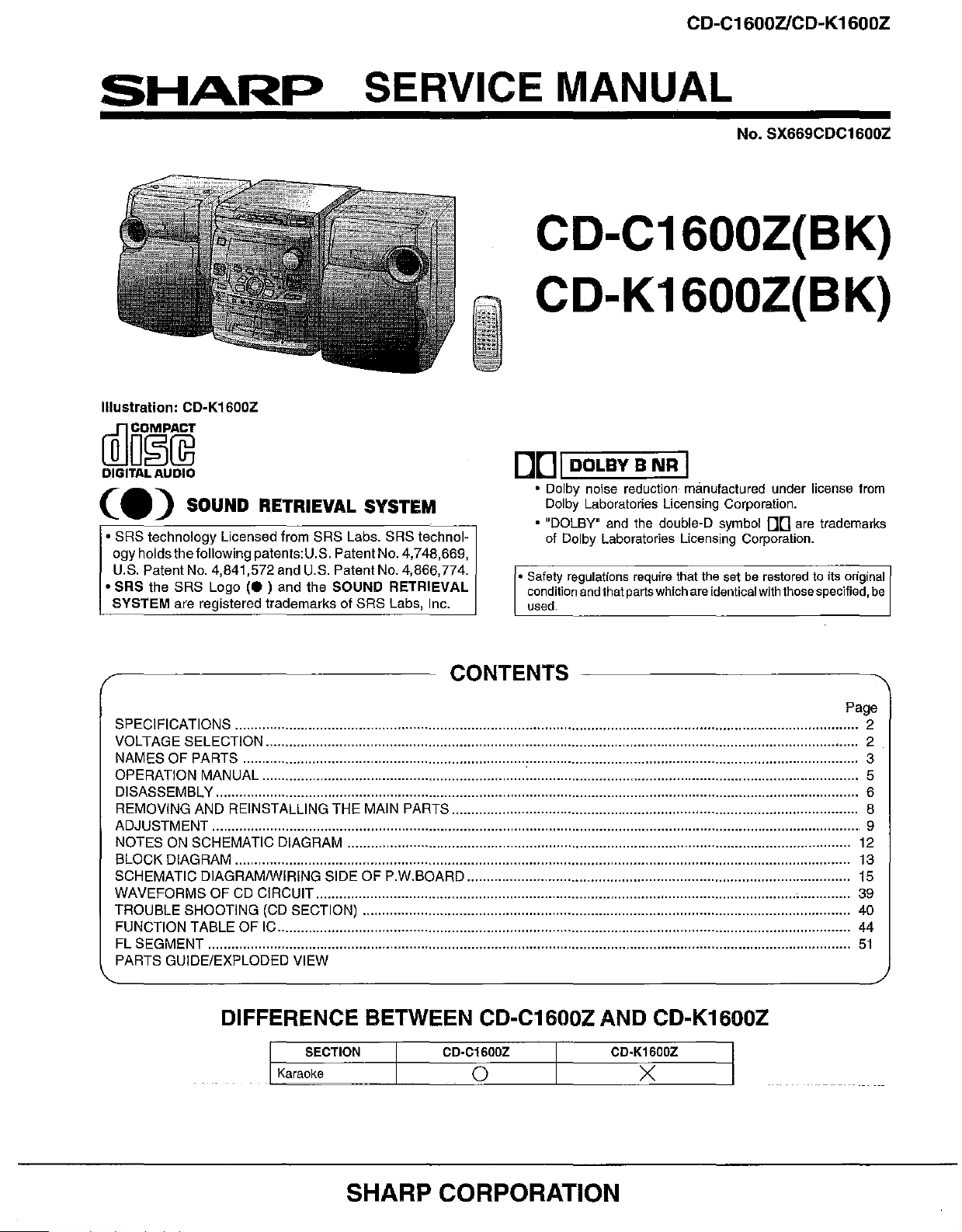
SHARP
Illustration: CD-K1600Z
SERVICE MANUAL
(]]o~@
DIGITAL AUDIO
C.)
• SRS technology Licensed from SRS Labs. SRS technology holdsthe/ollowingpatents:U.S. PatentNo. 4,748,669,
U.S. Patent
• SRS the SRS Logo
SYSTEM
SOUND RETRIEVAL SYSTEM
No.
4,841,572 and U.S. Patent No. 4,866,774.
(e)
and the SOUND RETRIEVAL
are registered trademarks of SRS Labs, Inc.
No. SX669CDC1600Z
CD-C1600Z(BK)
CD-K1600Z(BK)
DDI
•
DOLBYBNR
•
Dolby
Dolby
• "DOLBY"
of
Dolby
Safety
regulations
condition
used.
and
noise
reduction
Laboratories
and
the double-D symbol
Laboratories
require
that
parts
I
manufactured
Licensing
Licensing
that
which
are
Corporation
under
OD
Corporation.
the
setberestoredtoits
identical
with
.
are
those
license
trademarks
specified,
from
original
be
CONTENTS
Page
SPECIFICATIONS 2
VOLTAGE SELECTION 2
NAMES OF PARTS 3
OPERATION MANUAL
DISASSEMBLY 6
REMOVING AND REINSTALLING THE MAIN PARTS 8
ADJUSTMENT 9
NOTES ON SCHEMATIC DIAGRAM 12
BLOCK DIAGRAM 13
SCHEMATIC DIAGRAMIWIRING SIDE OF P.W.BOARD 15
WAVEFORMS OF
TROUBLE SHOOTING (CD SECTION) 40
FUNCTION TABLE OF IC 44
FL SEGMENT
PARTS GUIDE/EXPLODED VIEW
CD
CIRCUIT 39
: 5
51
DIFFERENCE BETWEEN CD-C1600Z AND CD-K1600Z
I SECTION
Karaoke
CD-C1600Z
o
CD-K1600Z
x
SHARP CORPORATION
CD-C1600ZlCD-K1600Z
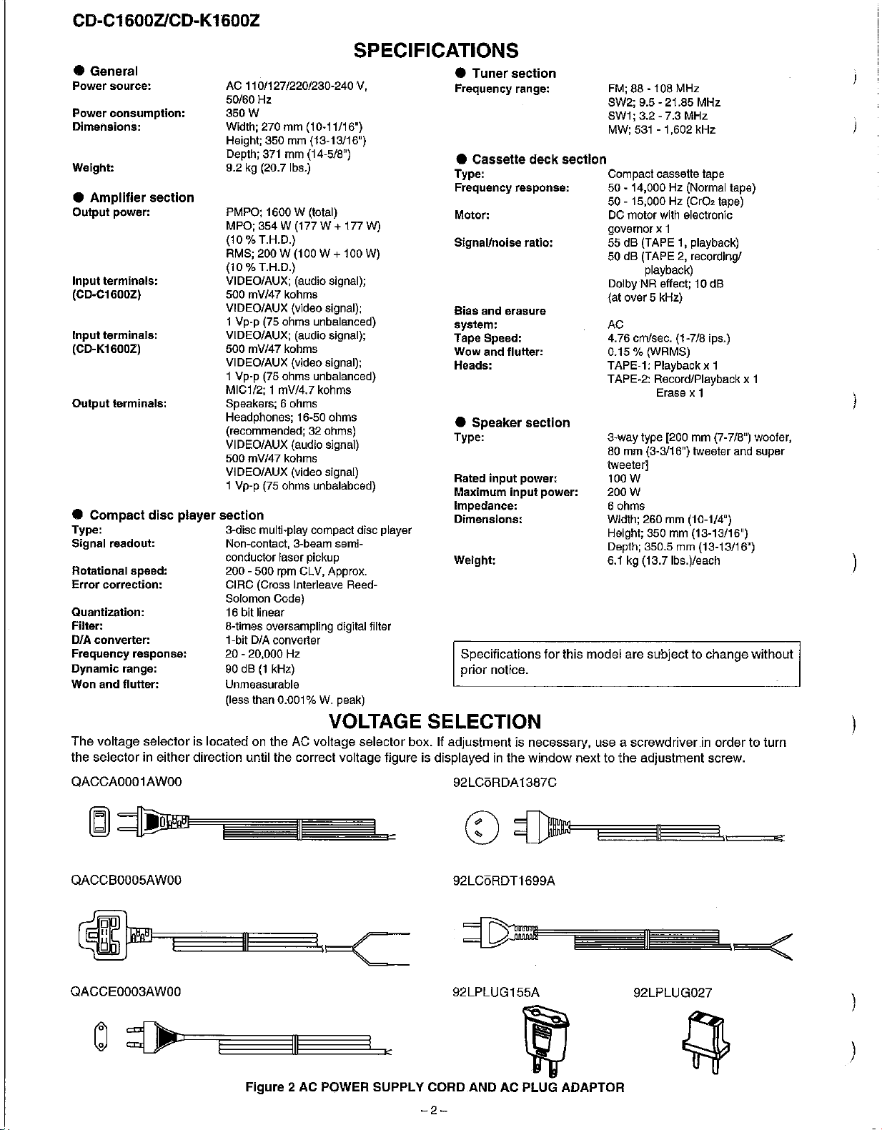
SPECIFICATIONS
•
General
Power source:
AC
110/127/220/230-240 V,
50/60 Hz
Power consumption:
Dimensions:
Weight:
Amplifier
•
Output power:
Input terminals:
section
(CD-Ct600Z)
350W
Width; 270 mm (10-11/16")
Height; 350
Depth;
371
mm
mm
(13-13/15")
(14-518")
9.2kg(20.7Ibs.)
PMPO;
1600 W (total)
MPO;
354 W
(l77W
(10
% T.H.D.)
RMS;
(10
% T.H.D.)
200 W
(100
+ 177W)
W + 100
VIDEO/AUX; (audio signal);
500 mV/47 kohms
W)
VIDEO/AUX (video signal);
1Vp-p
(75
Inputterminals:
(CD-K1600Z)
VIDEO/AUX; (audio signal);
500 mV/47 kohms
ohms unbalenced)
VIDEO/AUX (video signal);
1
Vp·p
(75 ohms unbalanced)
MICl/2; 1mV14.7 kohms
Output
terminals:
Speakers; 6 ohms
Headphones; 16-50 ohms
(recommended;32ohms)
VIDEO/AUX (audio signal)
500 mV/47 kohms
VIDEO/AUX (video signal)
(75
1 Vp-p
•
Compact
Type: 3-disc multi-play compact disc player
Signal
Rotational speed:
Error correction:
readout:
disc
player
section
Non-contact, 3-beam semi-
conductor laser pickup
200 - 500
eiRe
ohms unbalabced)
rpm
CLV, Approx.
(Cross Interleave Reed-
Solomon Code)
Quantization:
Filter:
D/A
converter:
Frequency response:
Dynamic range:
Won and flutter:
16 bit linear
8-times oversampling digital filter
1-bit D/A converter
20 - 20,000
90dB(1
Unmeasurable
(less than
Hz
kHz)
0.001%W.
peak)
VOLTAGE SELECTION
The
voltage
the
selectorineilher
selectorislocatedontheACvoltage
direction
until
the
correct voltage
selector
figureisdisplayedinthe
•
Tuner
Frequency
•
Cassette
Type: Compact cassette tape
Frequency response:
Motor: DC motor with electronic
SignaVnoise ratio:
Bias and erasure
system:
Tape Speed:
Wow
and flutter:
Heads:
•
Speaker
Type:
Rated input power:
Maximum input power:
Impedance:
Dimensions:
Weight:
Specifications
prior notice.
box. If
adjustmentisnecessary,
section
range:
deck
section
window
for
FM;88-108
SW2;
SW1; 3.2
MW;
9.5
- 21.85 MHz
-7.3
531
- 1,602 kHz
MHz
MHz
section
50
- 14,000Hz(Normal tape)
50
- 15,000Hz(CrO, tape)
governor
55
50
x1
dB (TAPE1,playback)
dB (TAPE2,recordingl
playback)
Doiby NR effect;
10
(at over 5 kHz)
AC
4.76 cm/sec. (1-7/8 Ips.)
% (WRMS)
0.15
TAPE-1: Playback x 1
TAPE-2: Record/Playback x 1
Erase x 1
3-way type [200
80
mm
(3-3/16") tweeter
tweeter]
mm
100W
200W
6 ohms
Width; 260
Height;
Depth; 350.5
350
mm
mm
mm
(10-1/4")
(13-13/16")
(13-13/16")
6.1kg(13.7Ibs.)/each
this
model
are
subjecttochange
useascrewdriverinordertoturn
nexttothe
adjustment
dB
(7-7/8") woofer,
and
super
without
screw.
QACCA0001AWOO
QACCB0005AWOO
QACCE0003AWOO
Figure2AC
POWER
SUPPLY
92LCijRDA
92LCijRDT1699A
92LPLUG155A
CORD
ANDACPLUG
-2-
1387C
92LPLUG027
)
ADAPTOR
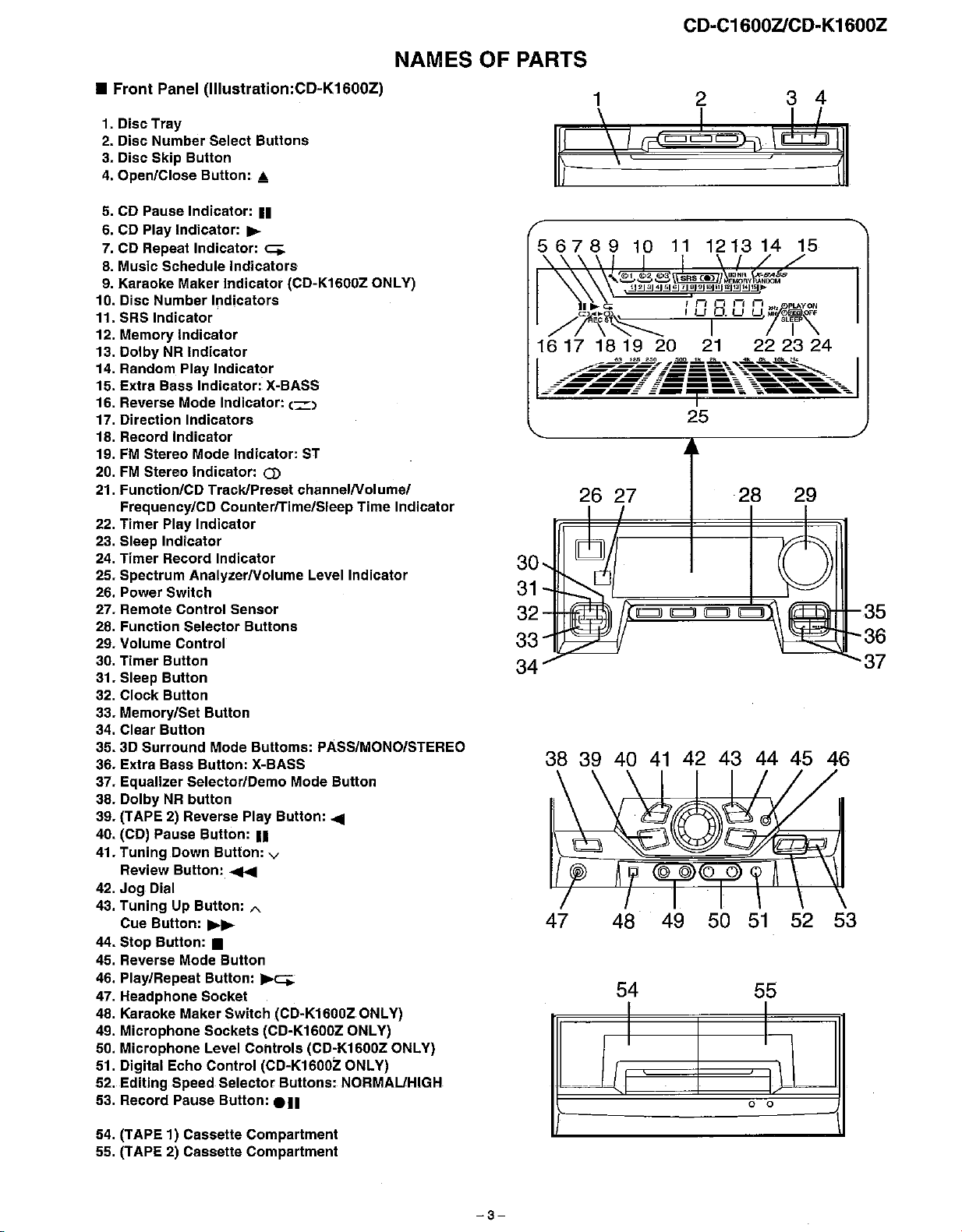
CD-C1600ZlCD-K1600Z
•
Front
Panel
(1IIustration:CD-K1600Z)
1. Disc
2.
3.
4.
5.CDPause Indicator:
6.CDPlay
7.CDRepeat Indicator:
B.
9.
10. Disc
11. SRS
12. Memory
13.
14. Random Play
15. Extra Bass Indicator: X-BASS
16. Reverse Mode Indicator: c:::)
17. Direction
1B.Record
19.FMStereo Mode Indicator:
20.FMStereo Indicator:
21. Function/CD Track/Preset
22. Timer Play
23. Sleep
24.
25.
26. Power Switch
27. Remote Control Sensor
28.
29. Volume Control
30.
31. Sleep
32.
33. Memory/Set
34. Clear
35.30
36. Extra Bass
37. Equalizer Selector/Demo Mode
38.
39. (TAPE2)Reverse Play
40. (CD) Pause
41.
42.
43.
44. Stop
45. Reverse Mode
46. Play/Repeat
47. Headphone Socket
48. Karaoke Maker Switch (CD-K1600Z ONLY)
49.
50.
51. Digital
52.
53. Record Pause
Tray
Disc
Number
Disc Skip
Open/Close BUllon:
Music Schedule
Karaoke Maker
Number
Indicator
DolbyNRIndicator
Frequency/CD CounterlTime/Sleep
Indicator
Timer
Record
Spectrum
Function
Timer
Bullon
Bullon
Clock
Bullon
Bullon
Surround
DolbyNRbullon
Tuning
Review
Jog
Dial
TuningUpBullon:
Cue
Bullon:
Bullon:
Microphone
Microphone
Edillng
Select
Bullon
Indicator:
Indicator
Indicators
Indicator
Indicator
AnalyzerNolume
Selector
Bullon
Mode
Bullon:
Bullon:
Down
Bullon:
~
Bullon:
Sockets
Level Controls (CD-K1600Z ONLY)
Echo
Control (CD-K1600Z ONLY)
Speed Selector
Bullons
..
..
~
<::;+
Indicators
Indicator
Indicators
Indicator
CD
Indicator
Bullons
Bulloms:
X-BASS
..
Bullon:
.........
A
•
Bullon
~
(CD-K1600Z ONLY)
Bullon:
(CD-K1600Z ONLY)
ST
channelNolume/
Level
PASS/MONO/STEREO
Bullon
Bullon:
v
Bullons:
e
....
..
Time
Indicator
NORMAUHIGH
NAMES
Indicator
OF
PARTS
30
31
32-ll-hm;'i\1
33~~
34
1
\
\ I
\
I~
56789101112131415
25
26 27
38 39 40
47 48
41
42 43 44 45 46
49
54
I I
I
I
50
28
~~36
51
55
I
I \
o 0
29
f1CEj';\\-HI-35
37
52
53
54. (TAPE 1) Casselle Compartment
55. (TAPE 2) Casselle Compartment
-3-
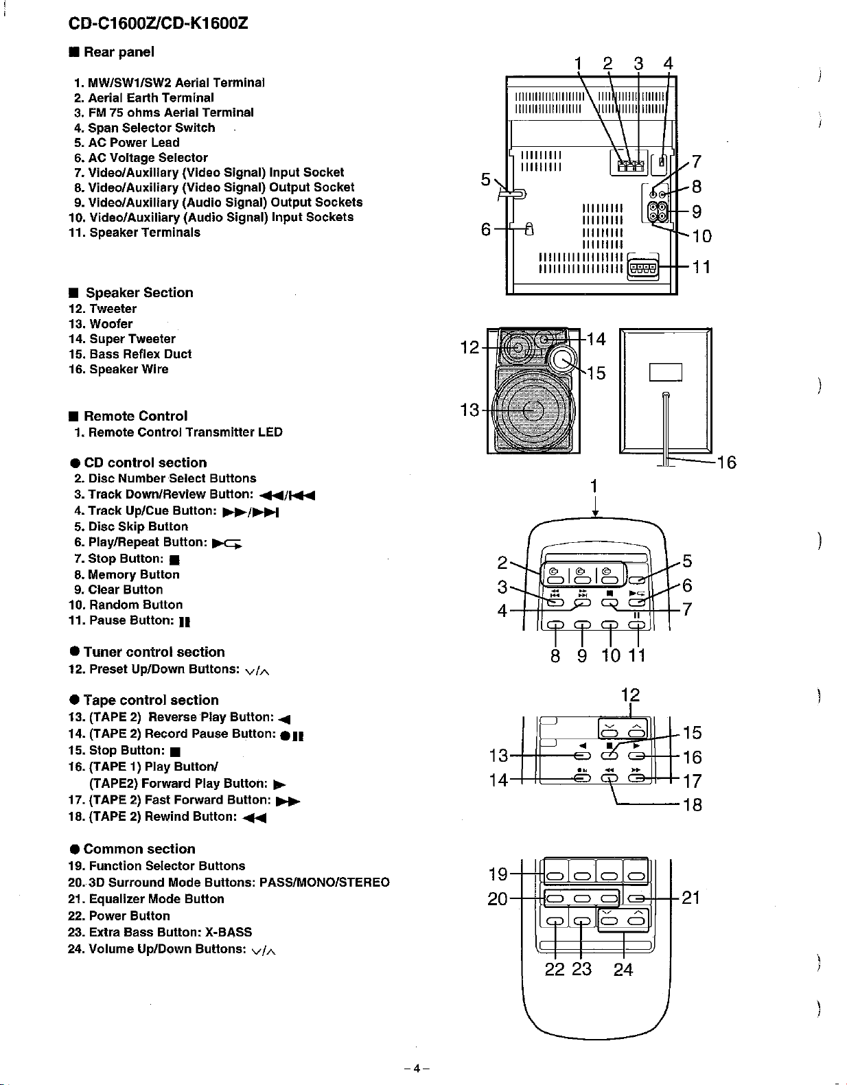
CD-C1600ZlCD-K1600Z
•
Rear
panel
1.
MW/SW1/SW2 Aerial Terminal
2.
Aerial Earth Terminal
3.FM75
4. Span Selector Switch
5. AC Power Lead
6.
7.
8.
9. Video/Auxiliary (Audio Signal) Output Sockets
10. Video/Auxiliary (Audio Signal) Input Sockets
11. Speaker Terminals
•
12. Tweeter
13. Woofer
14. SuperTweeter
15. Bass Reflex Duct
16. SpeakerWire
ohms Aerial Terminal
AC Voltage Selector
Video/Auxiliary (Video Signal) Input Socket
Video/Auxiliary (Video Signal) Output Socket
Speaker
Section
12
111111111111111111111
11111111111111111111
111111111
111111111
5
IIIIIIII1111111111
111111111 111111111
1 2 3 4
111111111
111111111
111111111
111111111
'''l''11U-9
~
14
15
D
7
8
10
11
Remote
•
1. Remote Control Transmitter LED
• CD
2.
Disc NumberSelect Buttons
3. Track Down/Review Button:
4. Track Up/Cue Button:
5.
Disc
6.
Play/Repeat Button:
7.
Stop Button: •
8.
Memory Button
9. Clear Button
10. Random Button
11. Pause Button:
•
Tuner
12. Preset Up/Down Buttons:
•
Tape
13. (TAPE2)Reverse Play Button: ....
14. (TAPE2)Record Pause Button:
15. Stop Button: •
16. (TAPE 1) Play
(TAPE2) Forward Play Button:
17. (TAPE2)Fast Forward Button:
18. (TAPE2)Rewind Button:
Control
control
Skip
control
control
section
.....
~/~
Button
~
••
section
viA
section
Button/
...
~
.....
/~
•••
13
13
14
1
2
3
4
10
9
8
11
5
6
7
12
..
0'.
- -
15
16
17
18
•
Common
19. Function Selector Buttons
20. 3D Surround Mode Buttons: PASS/MONO/STEREO
21. Equalizer Mode Button
22. Power Button
23. Extra Bass Button: X-BASS
24.
Volume Up/Down Buttons:
section
viA
-4-
19
20
-
- -
=1=1=
===
r-:olnllo
2223
24
=
=
~
21
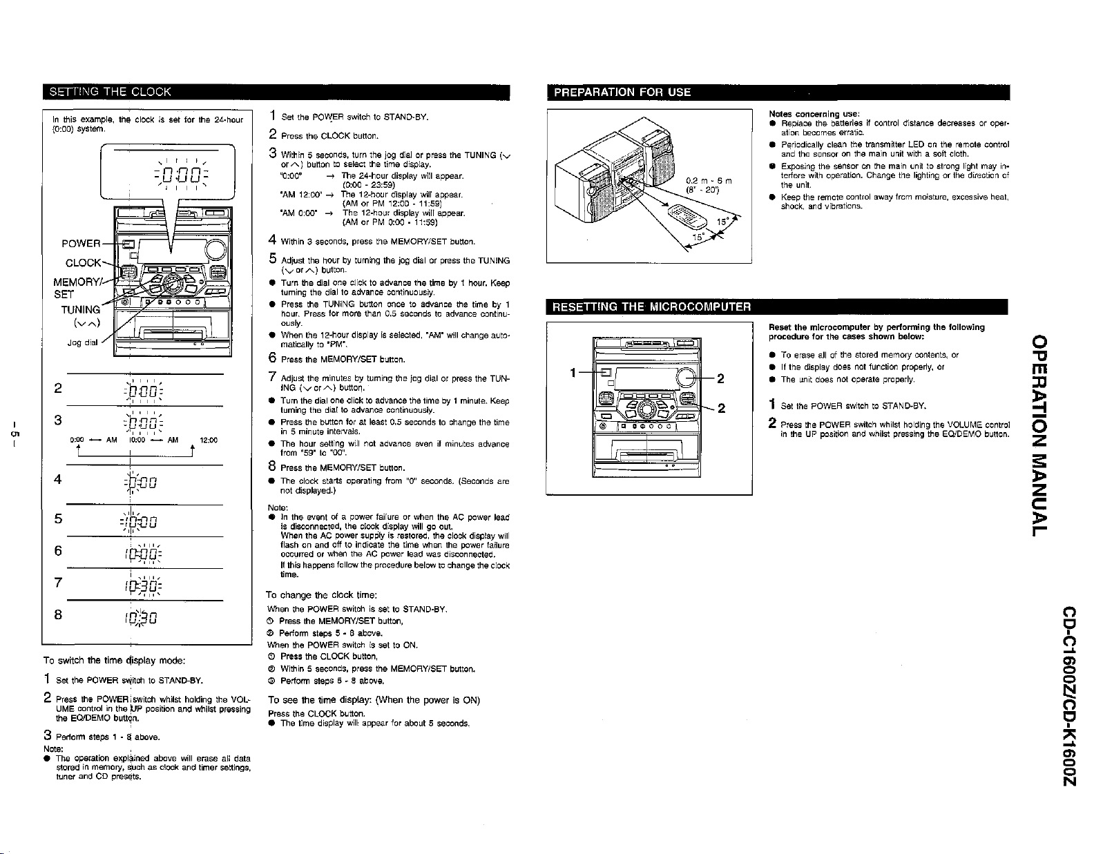
SETIING
In
(0:00)
this example,
system.
THE CLOCK
POWERB~
CLOCK
MEMORY/-
T~E::
=~I
2
3
I
'"
I
0;00_AM
I
t
4
5
6
7
8
To switch the time clisplay mode:
1
set
the POWER switch to STAND-BY.
2
PresS
the POWER i switch whilst holding the VOL-
UME control
the eQIDEMO butlqn.
in
3 Perform steps 1 • aabove.
Note:
•
The
operation
stored in memory, !:juchasclock and timer settings,
luner and CD
the!
clockisset for the 24"hour
...
I I I
1..-
-
n.n
n-
-U'UU-
...
I I I
I'"
~
..
' I , "
nn
-b
-
-
'uu-
",
I I
,"
,,'
, I
I,
=,ono=
I I "
10:00_AM
,
-'--
-
-nn
-
-uu
11'
','
,J,"",
-In-nn
-ru-uu
''i'-
..
" I ,
I fi..n
n-
ILrUU-
,'"I
..
--
I.." I ,
I
D::3
0=
I'"I
..
In'!~n
u"j U
theUPposition and whilst pressing
expl~ined
above will erase all data
presetts.
12:00
t
1 Set the PO""!'ER switch to STAND-BY.
2 Press the CLOCK button.
3 Within 5 seconds, turn the jog
orA)
button to select the time display.
'0:00"
'AM
'AM 0:00"
-+ The 24-hour display will appear.
12:00"-+The 12-hour display will appear.
(0:00 - 23:59)
(AM
-+
The 12·hour display will appear.
(AM
dialorpress
orPM12:00 -11:59)
orPM0:00 • 11:59)
the
TUNING
4 Within 3 seconds, press the MEMORY/SET button.
S Adjust the hour by turning the jog dial or press the TUNING
(vorA)
• Turn the dial one click to advance the time by 1 hour. Keep
• Press the TUNING button once to
• When the 12-hour display
button.
tuming the dial to advance continuously.
hour. Press for more than 0.5 seconds to advance continu-
ously.
matically to
'PM'.
advance the time by 1
is
selected. "AM" will change auto-
6 Press the MEMORY/SET button.
7 Adjust the minutes by turning the jog dial or press the TUN-
ING
(vorA)
• Turn the dial one click to advance the time by
turning the dial to advance continuously.
• Press the button for at least 0.5 seconds to change the time
in
5 minute inteNals.
• The hour setting will not advance even if minutes advance
from "59" to "00".
button.
1 minute. Keep
8 Press the MEMORY/SET button.
"0"
• The clock starts operating from
not displayed.)
Note:
• In the eventofa power failure or when the AC power lead
is disconnected, the clock display will go out.
When the AC power
flash on and off to indicate the lime when the power failure
occurred or when the AC power lead was disconnected.
If
this happens follow the procedure below to change the ciock
time.
To
change the clock time:
When the POWER switch is set to STAND·BY.
G>
Press the MEMORY/SET button,
@ Perform steps 5 • a above.
When the POWER switch
G)
Press the CLOCK bullon,
@ Within 5 seconds, press the MEMORY/SET button.
@)
Perform steps 5 • a above.
To
see the time display: (When the powerisON)
Press the CLOCK button.
• The tIme display will appear for about 5 seconds.
supply is restored, the clock display will
is
set to ON.
seconds. (Seconds are
PREPARATION FOR USE
concerning
Notes
• Replace
ation becomes erratic.
• Periodically clean the
(v
0.2m-Sm
(8"
- 20')
15·
RESETTING
THE
MICROCOMPUTER
=
1
2
2
and the sensor
• Exposing the sensor
terfere with operation. Change the lighting
the unit.
• Keep the remote control away from moisture, excessive heat,
shock, and vibrations.
Reset
the
procedure
• To erase allofthe stored memory contents, or
If
the display does not function properly, or
•
• The unit does not operate properly.
1
Setlhe
2 Press the POWER switch whilst holding the VOLUME control
in
theUPposition and whilst pressing the EQ/DEMO button.
use:
the batteriesIfcontrol distance decreases or oper-
transm~ter
on
the main unit with a soft cloth.
on
mIcrocomputerbyperforming
for
the
cases
POWER switch to STAND-BY.
LEDonthe remote control
the main unit to strong light may in·
shown
below:
or
the direction of
the
following
o
"C
m
:II
~
o
z
is:
~
z
c:
~
,...
o
9
o
...
~
~
C
,
...
"
en
c
~
CD-C1600ZlCD-K1600Z
DISASSEMBLY
CautiononDisassembly
Follow the below-mentioned notes when disassembling
to
the unit and reassembling it,
keep it safe and ensure
excellent performance:
the
unit.
they
unit.
the
need be
1. Take casselle tape and compact disc out of
power
2. Be sure to remove the
outiet before starting
3. Take off nylon bands
to
or
supply plug from
disassemble
the
wireholders where
removed when disassembling the unit. After servicing
the unit, be sure to rearrangethe leads where they were
before disassembling.
4.
Take
suff cient care on static electricity of integrated
circuits and other circuits when servicing.
STEP
1
2
REMOVAL
Top
Cabinet
Side
Panel
PROCEDURE
1.
Screw .......................
1.
Screw .....................
(Bl)
(Al)
FIGURE
x4
xl0
(LefVRight)
CD
Player
UniV
1.
3
CD Tray Cover open
Turnonthe
theCDtray
(Note
2.
Hook
3.
Hook
4.
Socket .....................
4 Back Board 1. Screw ......................
5
Main
Tuner
PWBI
PWBI
1. Screw .......................
2.
Socket .....................
power
the
disc
tray,
cover,
1)
........................
........................
supply,
take
out
and
close.
(Cl)
x3
(C2)
x2
(C3)
x4
(Dl)
xB
(El)x26-3,7-1
(E2)
x4
(CD-C1600Z)
2.
Socket ......................
(E2)
x5
(CD-K1600Z)
3.
Flat Cable .................
6
Front
Headphones
7
Karaoke
(CD-K1600Z
B
Jog
Jog
Display
9
Switch
10
Tape
11
Power
12
Turnt9.
13
Disc Tray
14
CD
Mechanism
15
CD
Sensor PWB
16
Panel!
PWB
Knobl
Switch
PWBI
PWB
Mechanism
Amp.
b1e
Changer
Mechanism
1.
Screw .......................
PWB
2.
Screw ......................
1.
Screw
Only)
1.
Knob
2.
Nul..........................
1.
Screw......................
i.0pen
2.
Screw
PWB
1. Screw ......................
1.
Screw
2.
Cover
1.
Screw
2.
Guide A ...................
3.
Guide
1.
Screw .......................
1.
Screw
1.
Screw
2.
Socket .....................
..................... (Gl)
.......................
the
cassette
.......................
......................
.......................
......................
B ...................
...................... (01)
......................
Note 1: Ifthe powersupplycannot beturned on,
(E3)
(Fl)
(F2)
(Hl)xl
(H2)
(Jl)
holder.
(Kl)
(L1)x7
(Ml)
(M2)
(Nl)
(N2)
(N3)
(Pl)
(Rl)
(R2)
<A>
x2
x3
x2
x2
xl
x15
x6
xl
xl
x4
x2
x2
x4
xl
xl
xl
7-2,7-3
7-2,7-3
7-2,7-3
7'2,7-3
turnthe
gearbyhand as shown in Figure 6-2 to open the disc
tray.
wall
6-1
6-1
6-2
7-3
6-2
7-2
7-3
7-2
7-4
7-4
7-5
7-5
7-5
(Bl)xl
03
Side
(Right)
(Bl)x2
03
x12mm
(Bl)x2
03
x10mm
CD
Player
Unit
Back
Board
(Dl)x8
la3
x10mm
CD-C1600Z
( E2 ) x2
Power Supply
PWB
x12mm
Panel
( E2 )
( E2 )
(Al)x2
03-x12mm
Top
Cabinet
(Bl)x2
03
x10mm
Figure
6-1
Figure
6-2
x1
X-",1,v~"[-~
---71bc------
Side
(Left)
(Bl)x3
/Zl3x12mm
Front Panel
Main
PWB
Panel
)
)
• SPEAKER SECTION
STEP REMOVAL
1
Front
Panel 1. Net ...........................
2 Speaker
PROCEDURE
2.
Rubber ..................... (A2)
3.
Screw ......................
1.
Screw
....................
(Al)
'(A3)
(Bl)xl0
xl
x4
x4
FIGURE
7-6
7-7
-6-
Figure
(E1) x2
03x10mm
6-3
CD·K1600Z
Power
PWB
CD·C1600Z
(L1)x4
03x10mm
( E2 ) x2
( E2 )
Supply
x2~-Oii~
(E2)
x;,1~","",
Figure
Switch
od
]I;e!~~~~~~
(l1
03
7·1
PWB
)x3
x10mm
---Alcr--
~
(E3)
Display
PWB
Front Panel
Headphones
,..open
PWB
Tape Mechanism
PWB
(F2)x2
03
x10mm
(E1) x2
03
x1
(H1)
(H2)x1
(F1)
03
x10mm
Main
PWB
x10mm
x1
x1
CD-C1600ZlCD-K1600Z
(Ml)x1
><
03xl0mm
(M2)x1
Turntabie
(Nl
)>:2
03xl0mm
CD
(R2)
Player Unit
Figure 7-4
(R1 )
03x10mm
(Q1)
x1
02.6 x10mm
Shift
Lever/l~JJ;;~~~';:
x1
(N2)x2
(P1)
x,
x1
03x14mm
)"
Sensor PWB
Care when installing the CD changer mechanism.
Installthe CD changer m3chanism on the
the shift lever has been set in the highest position.
Figure 7-5
CD
playerbaseafter
Figure 7-2
CD-K1600Z
(J1
)
x1
03
x10mm
Karaoke
(L1)
xl0mm (F1 )
03
PWB
(K1)
x6
03 xl0mm
x4
-:7''';-~~~~~~~~~~
4 ,..open
SwitchPWB
(ll
)
03
x10mm
Figure 7-3
- -- - Tape
x3
~
Display
Washer
PWB
(F2)
03
(E3)
Front
Headphones
PWB
x1
PWB
(H1 )
(H2)x1
Panel
03
x10mm
Mechanism
x2
x10mm
x1
x1
-7-
{A2)x4
a:
(81)X4
04xl0mm
~
Front
(Al)xl
Figure 7-6
Super Tweeter
{Bl)x2
",4x10mm
Pane!
Figure 7-7
Speaker
Woofer
Speaker
Box
Box
CD-C1600ZlCD-K1600Z
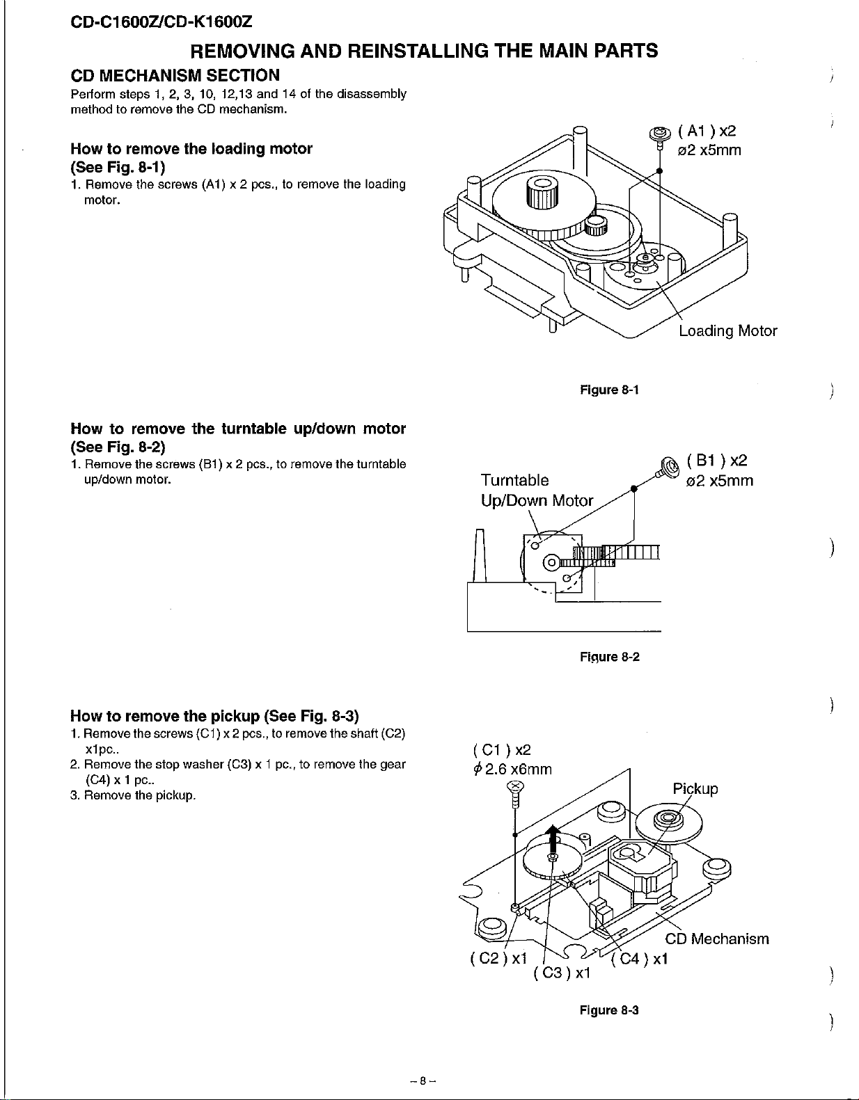
REMOVING AND REINSTALLING THE MAIN PARTS
CD MECHANISM SECTION
Perform steps 1, 2, 3, 10, 12,13
method to remove the CD mechanism.
How to remove the loading motor
(See Fig. 8-1)
1. Remove the
motor.
screws
(A1) x 2 pcs., to remove the loading
and14of the disassembly
Loading Motor
How to remove the turntable up/down motor
(See Fig. 8-2)
1. Remove the screws (81) x 2 pcs., to remove
up/down motor.
the
turntable
How to remove the pickup (See Fig. 8-3)
1. Removethe screws (C1) x2 pcs., to remove
x1pc
..
2.
Remove
(C4) x 1 pc
3.
Remove the pickup.
the
..
stop
washer
(e3) x1 pc., to remove the
the
shaft (C2)
gear
Turntable
Up/Down
(
C1)x2
</>2.6
x6mm
Figure
Motor
Fi~ure
B-1
B-2
(
B1)x2
02
x5mrn
-8-
Figure
(C4)
B-3
CD Mechanism
x1
CD-C1600ZlCD-K1600Z
MECHANISM SECTION
- Driving Force Check
Torque
Play: TW-2412 Tape1:Over 80 9
- Torque Check
Torque Meter
Play: TW-2111 30 to 60g.em 30 to 60 g.em
Fast forward: TW-2231
Rewind: TW-2231
-Tape
Speed
~
Normal
speed
TAPE
Volume MAX
3D
Surround Mode Button PASS
Pre-programmed Equalizer FLAT
Extra Bass OFF
Function TAPE
Dolby NR switch OFF
X-Bass OFF
RECORD
MODE
Meter Specified Value
Tape
2:
Specified
Tape 1 Tape 2
60 to
120
g.cm
60 to
120
g.cm 60 to 120 g.cm
Test
Tape
MTT-111
Adjusting
Point
VRM01 3.000 ± Speaker
SECTION
Position of each switch or control
UNIT
TP490@)PIN
/
OR(j)PIN
56q,kohms
"
560 ohms
Over 80 9
Value
60 to 120 g.em
Specified
Value
30 Hz terminal
Instrument
Connection
ELECTRONIC
VOLTMETER
LS:J
ADJUSTMENT
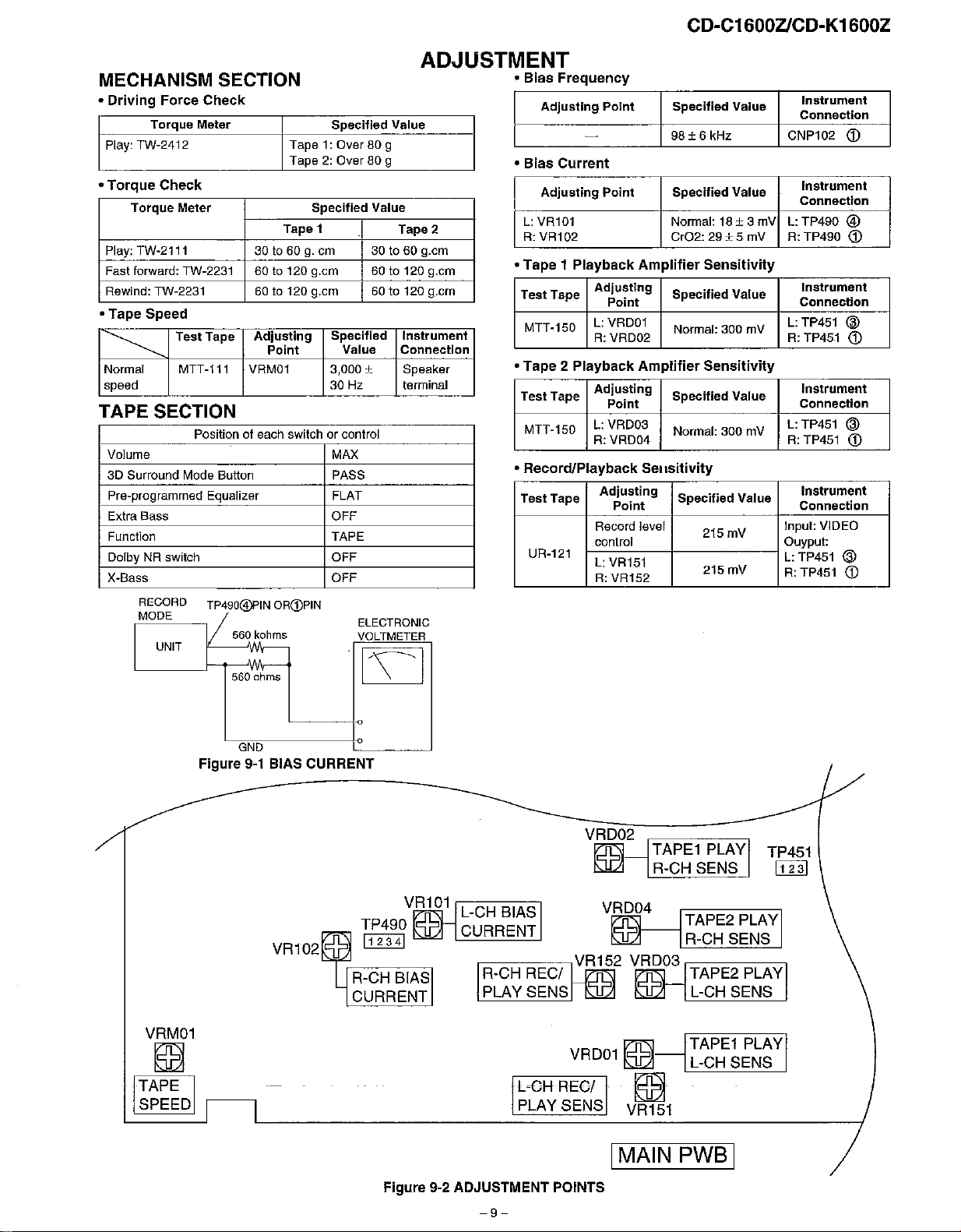
• Bias Frequency
Adjusting
• Bias Current
Adjusting
L:
VR101 Normal:
R:
VR102
- Tape 1 Playback
Test
Tape
MTT-150
- Tape 2 Playback
Test Tape
MTT-150
- Record/Playback
Test Tape
UR-121
Point
-
Point
Adjusting
Point
L:
VRD01
R:
VRD02
Adjusting
Point
L:
VRD03
R:
VRD04
Adjusting
Point
Record level
control
L:
VR151
R:
VR152
Specified
98±6kHz
Specified Value
Cr02:
Amplifier
Specified Value
Normal: 300
Amplifier
Specified Value
Normal: 300
Sensitivity
Specified Value
Value
18
± 3
29±5
mV
mV
Sensitivity
mV
Sensitivity
mV
215mV
215mV
Instrument
Connection
CNP102
Instrument
Connection
L:
TP490 @
R:
TP490
Instrument
Connection
L:
TP451 ®
R:
TP451
Instrument
Connection
L:TP451 ®
R:
TP451
Instrument
Connection
Input: VIDEO
Ouyput:
L:
TP451 ®
R:
TP451
(j)
(j)
(j)
(j)
(j)
GND
Figure 9-1 BIAS CURRENT
Figure
~--~VR152
R-CH REC/
PLAY SENS
r.-
"--:::O-=-H-=R=EO-=-/"
L
PLAY SENS VR151
9-2
ADJUSTMENT POINTS
-9-
VRD02
gg
TAPE1 PLAY
R-CH SENS
VRD04
OO~
~R-CHSENS
VRD03~---~
~
ill::
VRD01
~
ill::
gg
~.
IMAIN PWBI
TP451
~
ITAPE2 PLAYI
TAPE2 PLAY
L-CH SENS
TAPE1 PLAY
L-CH SENS
CD-C1600ZlCD-K1600Z
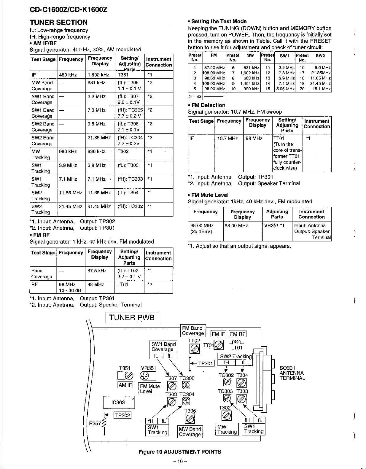
TUNER SECTION
flo Low-range frequency
fH: High-renge frequency
• AM IF/RF
Signal generator: 400 Hz 30%
MHz
MHz
dS
Frequency
1,602
531
3.2
7.3
9.5
21.85
990
3.9
7.1
11.65
21.45
Frequency
87.5
98
Stage
Sand
Sand
Sand
Sand
Sand
RF
Frequency
450
kHz
-
-
-
-
-
990
kHz
3.9
MHz
7.1
MHz
11.65
21.45
Frequency
-
98MHz
10-30
Test
IF
MW
Coverage
SW1
Coverage
SW1
Coverage
SW2
Coverage
SW2
Coverage
MW
Tracking
SW1
Tracking
SW1
Tracking
SW2
Tracking
SW2
Tracking
'1.
Input: Anlenna, Output: TP302
'2.
Input: Anetnna, Output: TP301
•
FM
Signal generator: 1 kHz, 40 kHz dev,
Test Slage
Band
Coverage
RF
'1.
Input: Antenna, Output: TP301
'2.
Input: Anetnna, Output: Speaker Terminal
, ,
Display
kHz
MHz
MHz
MHz
kHz
MHz
MHz
Display
kHz
MHz
kHz
MHz
MHz
MHz
AM
modulated
.
Adjusting
T351
(IL):
1.1
(IL):
2.0+0.1V
(IH):
7.7+0.2
(IL):
2.1+0.1V
(IH):
7.7
T302
(fL):
(fH):
(fL):
(fH):
FM
Adjusting
(IL):
3.7+0.1 V
LT01
Setting!
i>.
T306
+0.1 V
T307
TC305
T308
TC304
±0.2V
T303
TC303
T304
TC302
modulated
Settingl
Parts
LT02
Instrument
Connection
'1
'2
'2
'2
V
'2
'2
'1
'1
'1
'1
'1
Instrument
Connection
'1
'2
•
Selling
Keeping the TUNING (DOWN) button and MEMORY button
pressed, turn on POWER. Then, the frequency is initialiy set
in
button to
Preset
No.
21-40
FM
•
Signal generator'
Test
IF
'1.
'2.
FM
•
Signal generator: 1kHz, 40 kHz dev.,
98.00
(25
'1.
the Test Mode
the memory as showninTable. Cali it with the PRESET
Use
it for adjustment and check of tuner circuit
FM
Preset
No.
1 87.50
2 08.00
3
4 06.00
5 98.00
Input: Antenna, Output: TP301
Input: Anetnna, Output: Speaker Terminal
Frequency
Adjust so that an output slgnai appears.
MHz
MHz
90.00
MHz
MHz
MHz
Detection
Stage
Mute
Level
MHz
dB~V)
6
7
8
9
10 990 kHz
107
Frequency
10.7
MHz
Frequency
Display
98.00
1,602 kHz
1,404 kHz
MHz
MHz
MW
531
kHz
6Q3
kHz
FM
Frequency
Display
98
MHz
Preset
SW1
No.
11
3.2 MHz 16
12
7.3 MHz 17 21.85MHz
13
3.9 MHz 18 11.65 MHz
14
7.1
15
sweep
Adjusting
VR351
MHz
5.06 MHz 20 15.1 MHz
Setting!
Adjusting
Parts
IT01 '1
(Turn
the
corecf
trans
former TT01
fully counterclock wise)
FM
modulated
Parts
'1 Input: Antenna
Output: Speaker
Preset
No.
19
21.45 MHz
Instrument
Connection
w
Instrument
Connection
Terminal
SW2
9.5 MHz
ITUNERPWB I
T351
og~
IAMIFI
IC303
~
R357
j
IFM
IFIIFM
SW1
VR351
Band
Coverage
fL
fH
T307
~
~.
r~
TC305
IT01~
SW2
TC302 T304
~m
T308 TC304 TC303 T303
~
~06
~fHL,--fL-'<
SW1 SW1
Tracking Tracking
Figure 10 ADJUSTMENT POINTS
-10
~
-
T~~
-G6T
Trackin
fH
~~
~
RFI
IL
~
""IH--+L,
S0301
ANTENNA
TERMINAL
CD-C1600ZlCD-K1600Z
TEST MODE
•
Setting
Anyone
Hold down the MEMORY SET and CD buttons, and press the POWER switch. TEST: CD operation test
-TEST
Function
S~tting
Indication of CD
OPEN/CLOSE operation is manual operation.
T~e
the
test
of test mode can be set by pressing several keys as follows.
mode
mode
- CD
test
mode
of
TEST
mode
TEST
I IL is not performed.
pickup
canbemovedbyusing
<MEMORY>-When
key input lng servo is acti- STOP button. willreturnto key input ingservo is acti- key input mallyreturns to
mode (Fig. 11-1)
fhe
(~)or(~)
the
track--
vated,
playback
will beginatthe position. will beginatthe tion.
current position. current position.
Press the
key.
-The
the
]
pickup -
STOP
<MEMORY>-When
vated,
the
track--
playback
<STOP>-
The pickup nor-
the
STOP
posi-
<PLAY> key
Note:
Only in STOP state it is possible to slide the pickup with the
(~)or(~)key.
VOL. --- Last memory
BAL.
---
CENTER
R.GEQ.
X-BAS
Canceling method - POWER OFF
---
---
OFF
CD SECTION Figure
FLAT
input-
TOC. IL is performed, and the ordinary PLAY is performed. - Press <STOP> key. - Stop
If the following key is pressed during PLAY, it is possible
to specify directly any Track No.
<Disc Number
<Disc Number 2> key: Track 9
<Disc Number 3> key: Track 15
1> key: Track 4
:2?_
11
-1
Since thisCDsystem incorporates the following automatic adjustment function, when the pickup is replaced, it is not necessary
to
readjust it.
Since this
•
Automatic
1.
Focus offset (Fig. 11-2)
2.
Tracking offset (Fig. 11-3)
3.
ElF balance (tracking error balance) (Fig. 11-4)
CD
unit does not need adjustment, the combination of PWB and laser pickup unit is not restricted.
adjustment
item
4.RFlevel AGC function (HF level: constant)
5.
RF level automatic follow-up of the tracking gain
This automatic adjustment is performed each time a disc is changed. Therefore,
each disc is piayed back using the optimal settings.
0.1s
0.50 V
IC1@FD
O.ls
0.50'::1--.
IC1l.DTE
200ms
1V/diV
IC1
200ms
1V1diV
IC1(j)
Y
Y
,---,,----,--=,---.,----,-,-,--,
FIgure 11-2
@)
TO
TE
/
/'
I
FOCUS
OFF-SET
ADJUST
TRACKING
OFF-SET
ADJUST
1
2
TRACKING!
ERROR
BARANCE
1ADJUST
2
10m3
0.50V
IC1@FD
10ms
0.50V
1
IC
0
TE
Figure 11-4
-11
-
~
V
Figure 11-3
Enlarged
View
TRACKING
OFF-SET
ADJUST
1
2
CD-C1600ZlCD-K1600Z
NOTES ON SCHEMATIC DIAGRAM
• Resistor:
To differentiate the units of resistors, such symbol as K and
M are used: the symbol K means 1000 ohm and the symbol
M means 1000kohm and theresistor without any symbol is
ohm-type resistor. Besides, the one with "Fusible" is a fuse
type.
• Capacitor:
To indicate the unit of capacitor, a symbol P is used: this
symbol P means micro-micro-farad and the unit of the
capacitorwithoutsuch a symbol is microfarad. As toelectro-
lytic capacitor, the expression "capacitance/withstand volt-
age" is used.
(CH), (TH), (RH),
(ML): Mylar type
(P.P.): Polypropylene type
• Schematic diagram and Wiring Side of P.W.Board for this
model are subject to change for improvement without prior
notice.
REF. NO
SWI
SW2 OPEN/CLOSE
SW3 MECHA UP
SW4 PICKUP
SW202
SW701
SW702 MEMORY/SET
SW703 CLOCK
SW704
SW705 TIMER
SW706 POWER
SW707
SW708 REVERSE MODE
SW709 EDiT
SW710 HIGH
SW711
SW712
SW713 EO/DEMO
SW714 STOP
SW715 TUNING UP/CUE
SW716 PASS
SW717 MONO
SW718 STEREO
SW719
(UJ):
Temperature compensation
DESCRIPTION
DISC NUMBER
IN
SPAN SELECTOR
CLER
SLEEP
F-PLAY
REC PAUSE
X-BASS
VOLUME-UP
POSITION
ON-OFF
ON-OFF
ON-OFF
ON-OFF
50/9-100/10
ON-OFF
ON-OFF
ON-OFF
ON-OFF
ON-OFF
ON-OFF
ON-OFF
ON-OFF
ON-OFF
ON-OFF
ON-OFF
ON-OFF
ON-OFF
ON-OFF
ON-OFF
ON-OFF
ON-OFF
ON-OFF
ON-OFF
•The indicatedvoltage in each sectionis the one measured by
Digital Multimeter between such a section and the chassis
with no signal given.
1.Inthe tuner section,
( ) indicates AM
< > indicates
2.
In
the main section, a tape is being played back.
3.
In
the decksection, a tape is being played
( ) indicates the record state.
4.Inthe power section, a tape is being played back.
5.Inthe CD section, the CD is stopped.
• Parts marked
maintaining the safety of the set. Be sure
parts with specified
performance of the set.
REF. NO
SW720
SW721
SW722
SW723
SW724
SW725
SW726 CD
SW727
SW728
SW729
SW730 DISC 1
SW731
SW732
SW733
SW734
SW735
SWaOl
SWEI
SWE2
SWE3
SWE4
SWE7
SWE9
FM
stereo
with"
A"
( c ==:::J) are important for
ones for maintaining the safety and
DESCRIPTION POSITION
VOLUME-DOWN
TUNING DOWN/REV
CD PAUSE
R-PLAY
DOLBY
KARAOKE(CD-KI600Z ONLY)
TUNER
TAPE
VIDEO/AUX
OPEN/CLOSE
JOG
VOLTAGE SELECTOR
TAPE 2 SIDE A
TAPE 2 PLAY
TAPE 2 SIDE B
TAPE 2
TAPE 1
NR
DISC2
DISC3
DISC SKIP
Cr02
Cr02
TAPE 1 PLAY
FP
FP
DETECTION
DETECTION
baCk.
to
replace these
ON-OFF
ON-OFF
ON-OFF
ON-OFF
ON-OFF
ON-OFF
ON-OFF
ON-OFF
ON-OFF
ON-OFF
ON_OFF
ON-OFF
ON-OFF
ON-OFF
ON-OFF
ON-OFF
ON-OFF
ON~OFF
ON-OFF
ON-OFF
ON-OFF
ON-OFF
ON-OFF
)
ffi
ECB
(S)(G)(DI
II)
{21
131
2SA562 Y
2SC2001 L KTA1271 V
2SC23B9 SE KTA1273 Y
2SC2878 A KTC1026
2SC2878 B KTC3199
2SC535 C KTC3203 y
28D468
KRA107 M
KRC102 M
KRC104 M
KRe10? M
KTA1266-
C
FRCNTVlEW
CD
~.~~~
------
GR
GR
KV1236Z
23F
~
in
BeE
l~I\~i\~1
2881370
28D2012
Figure12TYPES OF TRANSISTOR AND LED
VIEW
~
*"
5N4GTN52
LMKD515B
-12-
131s8
(1}D
TOP
VIEW
DTC114 YK
G (2)
TOP
VIEW
IT]
188355
KDV147 C
to·
"
t:
iil
~
'"
Dl
,...
o
~
0 I
'"
;>;
I C I
-I
>1
"I
~I
s:
~
~
~
PI<I:KUP
-----------
FOaUSCOIL
----t1T'--
TRAC!'KING COIL I L
---I'Tr-
I
1_
UNIT
It
It
_____
M1
SPIN
MOTOR
M
-I
I
I
I
I
I
I
I
I
I
I
I
I
I
I
I
:
I
:
I
I
I
I
I
I
I
I
I
+5V
+5V
[64J
~
N
UU
~~ OEF
IC1
LA9240M
FIN2SERVO
2
FIN1
3 E
4 F
~i
:3X1oX19:I!3:I!S;
AMP.
SL+.
XL1
16.93MHz
C~
LC78625E
SERVO/
SIGNAL
CONTROL
CL, OAT, SELIAL CONTROL [ "
SL-.
ORF
I;DLDM+/CD LD M-/CD T. T/CDT.T STOP
IC2
+5V
caaca
caaca
5;>?(::iii:
RCHPIH'
RCHN '
LCHN~
LCHP
6
J
+5V
'8
IC3
NJM4565D
MICAMP
:4
IU:-;V.·
TO
TO
L,CH
tD,"",--
AUDIO
tD.JI OUT
R-CH
,
.
..;JIEM
MICON
SYSTEM MICON
CHANGER MECHA
..
TO
IC501
/
ICS
BAS920FP
-----..,
I
PICKUP
IN
SW4 .
{~I
DRIVER
q~-------~
...
+7.3V
-:
+73V
REGULATOR
:J
,.
o
c
•
o
...
8
~
c
•
....
'"
~
~
CD-C1600ZlCD-K1600Z
RP.F
rn
~
~,
-~
TERMINi\\.
,m
[g
[g
[g
,
l~
ICTOl
TA735ElAP
fMFRONTENO
,,~
t.
rn
~o
~e
010'
~~
,.,
"'00
E~~8~
'"
, "
j fflQMCDL\'llT I
T1S~
J~
AJLfi?~~
,~
TlPLAV
SOl.~@~~~-----"""'''''''''''-1
SWE2
T2PLAY
!TAPE'!
ITAPE2!
~
~,
~,
~-:_",-----------~---l-+-----1---4-1---+--~--4--+-"'-*I!=:;----i"---~:iii:;----"
MORlR
llRIVER
,,~
<
[....,.-
v-<>-j
'L.o-
.,.-+
Y..-.;,.-
v-<>-j
L.;;....~Ci
'L.o-
PllHE.o,r,
~~
~
AECII'B
HEAt>
.0:-8--1°'00
~~~~
_IIEe
~
---_~__'~"'""'OO"'"
~
IlRIVER
HISPE«~'
0133
Ql3-l
p.e
I
REC/PIl
01051 _ RNF<j :
0104
01061
TAPEMOTOA
'''"O<~''_1
"",O~~><_~"'e="'---,
'n"~""__1
T1/1l!SOlE!;OIIJ
12
PLAV
IC101
AN7345K
PLAVBACK&RECORDAMP.
l
: 1 •
l'
""
j A
_.
'
L~~\.i
/'OPflHJl.I~E~
'C<>-
I 5 PLAY-EW:K
r:
T1lT~
T
+,O<~"--,
0113
Ql14
p.1l.
P.B
4 L
~
.
......Im'l
REe
TllT2
vnool
vnOO2
~""
al~l
GllMUTE
VAOO3
vnOO4
MlITlNG
~alKll
§
BMlJTE
0=
MlJTtllI
SWIR:HIN3
ICD03
8A3311l
RECJP.8.
EQUALIZER
CO
TAPE
TUNER
rn,
,
"
,
,l
"
I..,
,
j='"
,
,
,
I
:
:
I
i
L
753114E
'16~Sll1
~
"
AUDIO ROCESSOR
r----c
GRAPHIC
c
EQlW.IZER
<
"':-:-,~";_.'~!:J~~;:'
ACIlIAS
VR10l t
~,
.
.
~
AJDUST
,~<
""r-~'-------jrN:
HEAil'~
all'"
.~~,
NOR! '!'
011D
011'
r;;;;;;I
BlASOSG. SWlTGHIHG
HIGH 11fT2
.I."e-~_
H15PEElJ I
0119
SWITCHING.
f---------'L('01.~
~,IO~"'''][$
0135 0133
~
~
0136 0134
0121
T11T2
~
o~
!~
HI5PHlJ
MiS
0128
5WITGH~G
-14
M"
""
(213)
-
REG
E
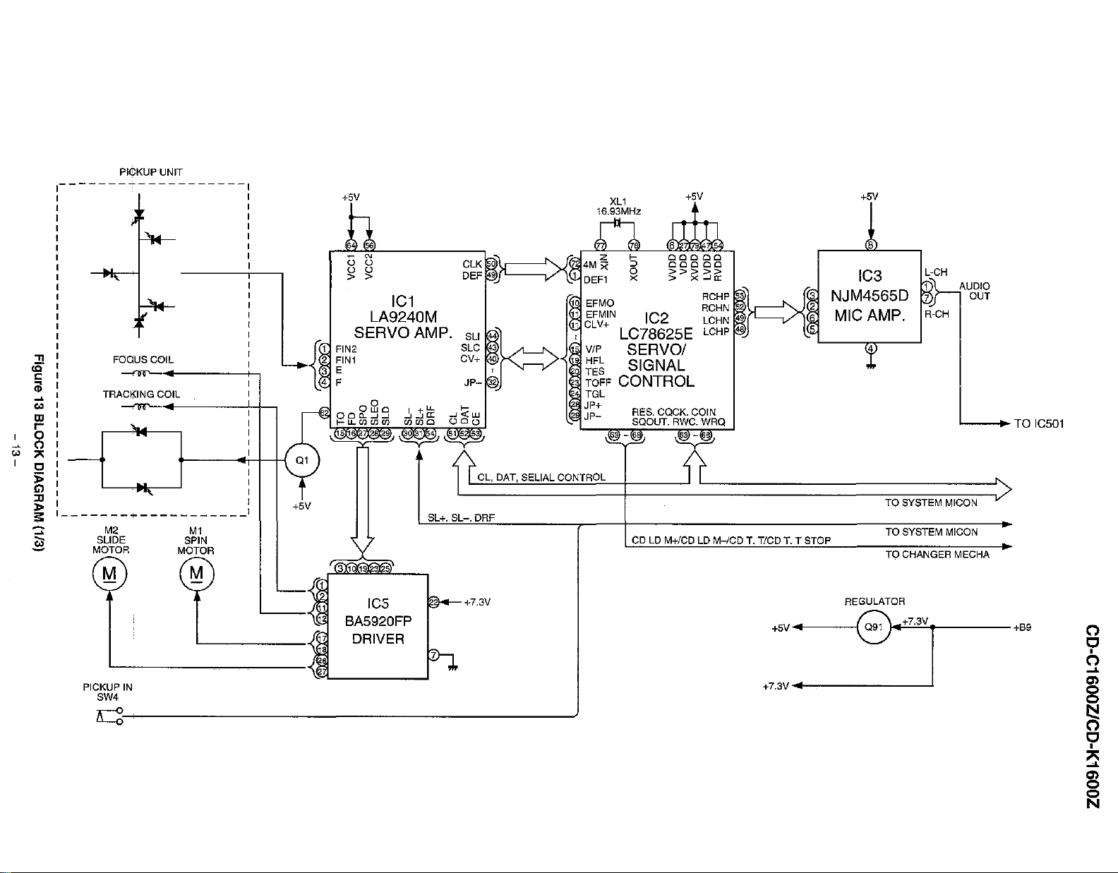
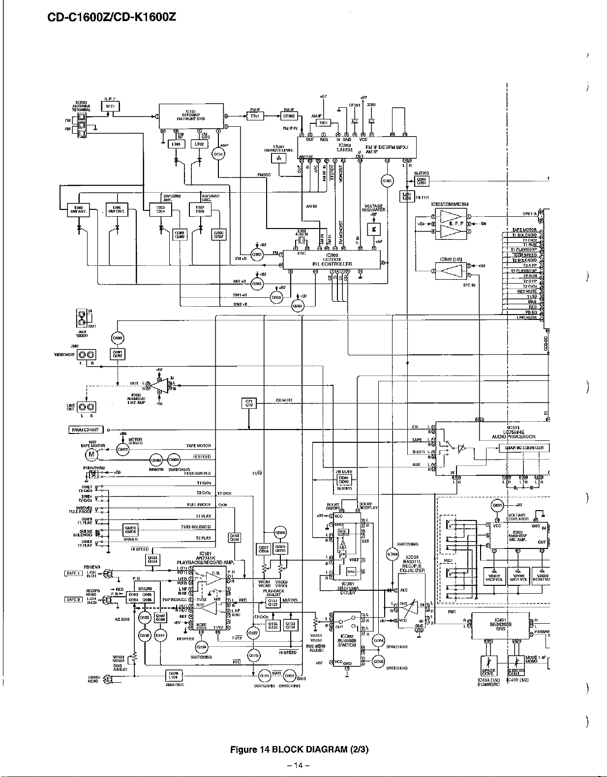
Figure 14 BLOCK DIAGRAM
",
PASSiSf
,
RMG101
REMOTE
SEt/SOIl
CD-C1600ZlCD·K1600Z
KEYIM,TIUX
1
,
TIIPEOOTOR
i
11
SOLENOID
i
, 11 PLAYI5TOP
~,
T2SDLENOID
: T2PLAYISTOP
'£IN
nEGMUTE
UNEMUIE
SJ'EI 5
TlCo<»
T1
T2AFP
T2RUN
T2BfP
n,~
,=
"~
PREQ
RUN
"~
l<
TlR'lERMUTE
~IPD7B045A
SYSTEM MICROCOMPUTER
IC201
CO-PUIN
P. FAll
lOWUt/ll
I
SWITCHIN3
j
CDLDM+
CDLDM-
LOADING MOTOR
DRIVER
L'".C'""'''"O."
DET
CDTIfClOSE
'~"~'~";o~"rn~=======:':i=3
~
f-""."'""O----------t-'-..--."~::I{O
I
CD
UP/lXlWN
1C!l1
TA7291S
~
-{~,
DRIVER
M
~
~
LOADING
MOTOA
~'k
CLOSE
i
-00
_00
-"-',"'-----1 •
+5V
UN-SWITCHEO
,00
-,'~'~~'~OO~m"'Ui~"
::
~~~"O"t-":Jl
VOLTAGE
REGURATER
VOl.TAGE
"ECURATE"
f--+-----j
aB25
"Bl~U~l"
VOlTAGE
REGULATOR
VOlTAGE
OB21
~,
'"
--t--+-------<~~~5
OB2a
SWITCHING
VOLTAGE
REGULATOR
Figure 15 BLOCK DIAGRAM (3/3)
-15
-
CD-C1600ZlCD-K1600Z
A
r-:--~----------.-,-----------------.:-------------:-~-----
B
c
~----------
1
~"
CNSUI
,
'h
,
, ,
r--
E 4
: '
,
,
,
,
,
,
,
,
,
,
,
,
,
,
,
-----------------;
j'"
,
:
!1-
Cl
~
;ji~
0.01
I---J
~1J2SKTA8~GR
.,
~
0.001
,_
R43
•.eo'I
22
'5"
!
,
~
me
,~
4~~
~
=
4.7150_
~
.,
~,
'oo
"'
,
j
!
I
1
~~~
,
l~~'~i~~i~~1
i
~,~
D
i-;;.:"
, 3
IA_
FO-
1
~
: 8 W
I
PICKUP
~._----------
E
UNIT
J.
&,
.--------,
,
,
,
•
:;
't
•
S GNO
•
t
~
F+
~
eo
VR
,
,
,
,
,
'"
.,
'"
~.
"
cr
~f
w7
~J~
=
"
V
o
,~
'"
'"
"'
'"
.,
FOCUSfTRACKINGI
SPIN/SLIDE DRIVER
[C5
BA5920FP
F
00
RL1G4A
.,
~
100110
.,
I:~"-:-'--I
MOTOR~-
'I
:;;:~-:
I 3 SL !
G
?IC~~IN
1
I
l.2P
MorgR
..
.
:u'
. 1 1 1 1
'~
PW12-.£Jij
l§
13
4
Sl.
.~:::.:
~~~~--J
PU~N
i
~
i5
L l _
~.
~,
""
'"
"
1S3'33
ft49
lL
1jloKl§
,
.,
,
00
I
~,
.
•.
=
I
,
:
I
,
r
,
,
:
,
,
I
I
,
I
:
:
!
00.
"m
,.
,
,
!
)
H
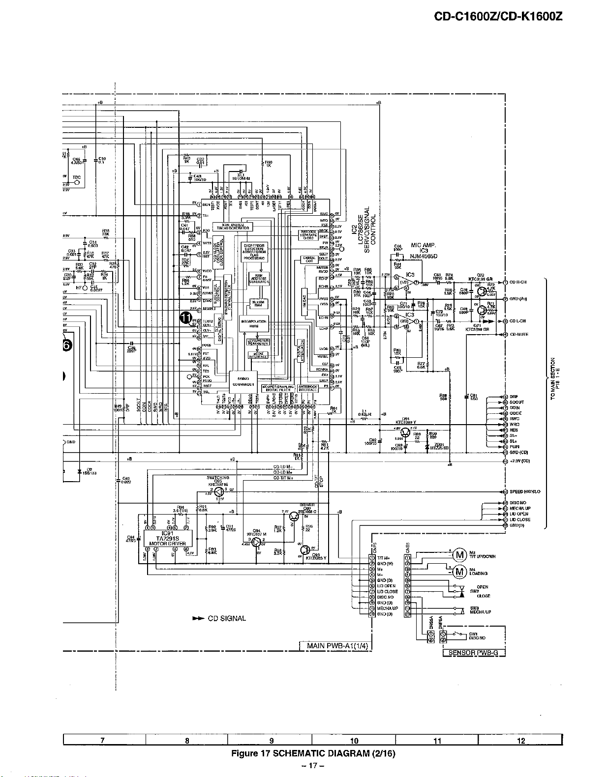
The
numbers.
NOTESONSCHEMATIC DIAGRAM can be found on page 12,
to
4B
are
waveform numbers showninpage
2 3 4 5
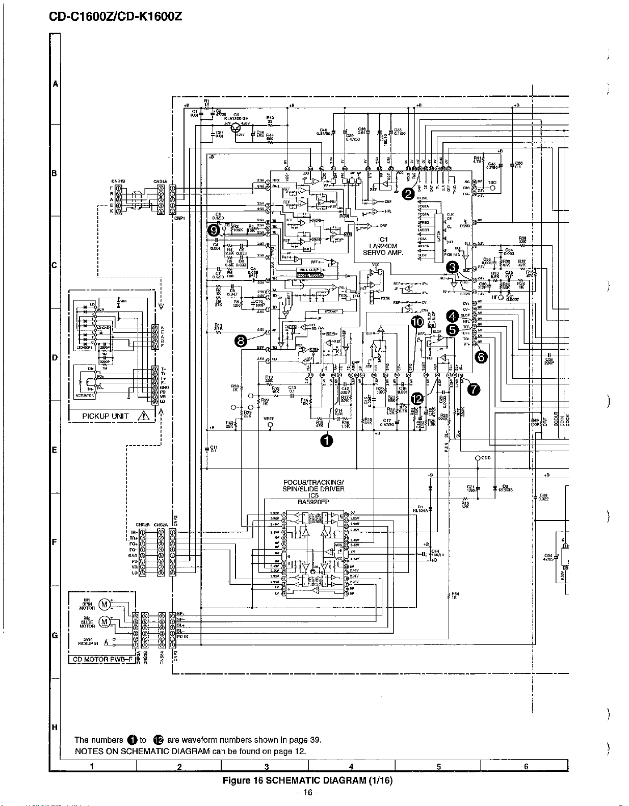
Figure 16 SCHEMATIC DIAGRAM (1/16)
-16
I
39.
6
-
,
------1------------------------------------,
2~<:&ln~j~
ow
2~~*
~""
w
+9
,
+O~,t43
~jl
C32
[lob7
1
R85
47Q
~rt
R3:l
5.8K 27P
~~~
HF6
CD-C1600ZlCD-K1600Z
+9
w,
KTCIIl99
GR
i
CilR.cH
4.1K
.>f!I
T
0-
G/{O(Aul
~~
.
!
.
CD
LoCH
Q"
KTC319\JGR
•
CD·MlJTE
~
1SS133
I
,
I
,
'~,
,~
-
w
4.7K
-
'"
"
CO-toM-eO-LDM.
094
~~~
..
v
'1t..,"
CO-TIfM+
7.'V
1.2K
""
w
3.3K
-
,
=
2004680
w
~
-
.~
rN
.~
.,
.
l(fg~3Y
r==~~=~~~g~~~~~I\fTM.~!--J
lU~~~A.~j
:-o~
',.v~
",
9~
~~
~
R92 091
47/25
T.J~:~1S
""
MOTOR
ORlVER
L
~!t·=i~.=~'r~·='boc~·~~·~~=~=!~====~
I
..
S.9K 47125
",
CD SIGNAL
_________________
.~.
';;"
100110
=,
100110
r----------------~
I~
:
~~D(M}
SGnD(D)
6
LID
OPEN
LID
CLOSE
DISCNO81--
9 GND(D) 9
MECHAUP
GNDeD)
H""
O~
'"
22
220
,
M~_6B
1J,l
3~~6ADING
_____
+ M
¥~UPIDOWN
~-
6
"
-Cd~..?PEN
=j::j=;::::::=:::;l
~ ~
O
i!&-.-.::
~OlSCNO
"
..
~
cLOSE
MECHIlUP
""
~---,
~.
~,
:=::.
~.
~,
:=::
~,
R,
oe>
'oo~
00'"
=,
~o
WOO
,,-
""
".
~'"
GnDICD)
+7.aV(CDI
I
,
SPEEO
DISCNO
MECftAUP
LlOOPEN
LID
G/{DlOI
!
CLOSE
HIGHll-O
z
0
~w
W'
wz.
~o::
g
bgtl§QfL~qJ
7
8
9
Figure 17 SCHEMATIC DIAGRAM
I 10 1
-17-
(2116)
__
-'-11'--
-'-'12'--
__
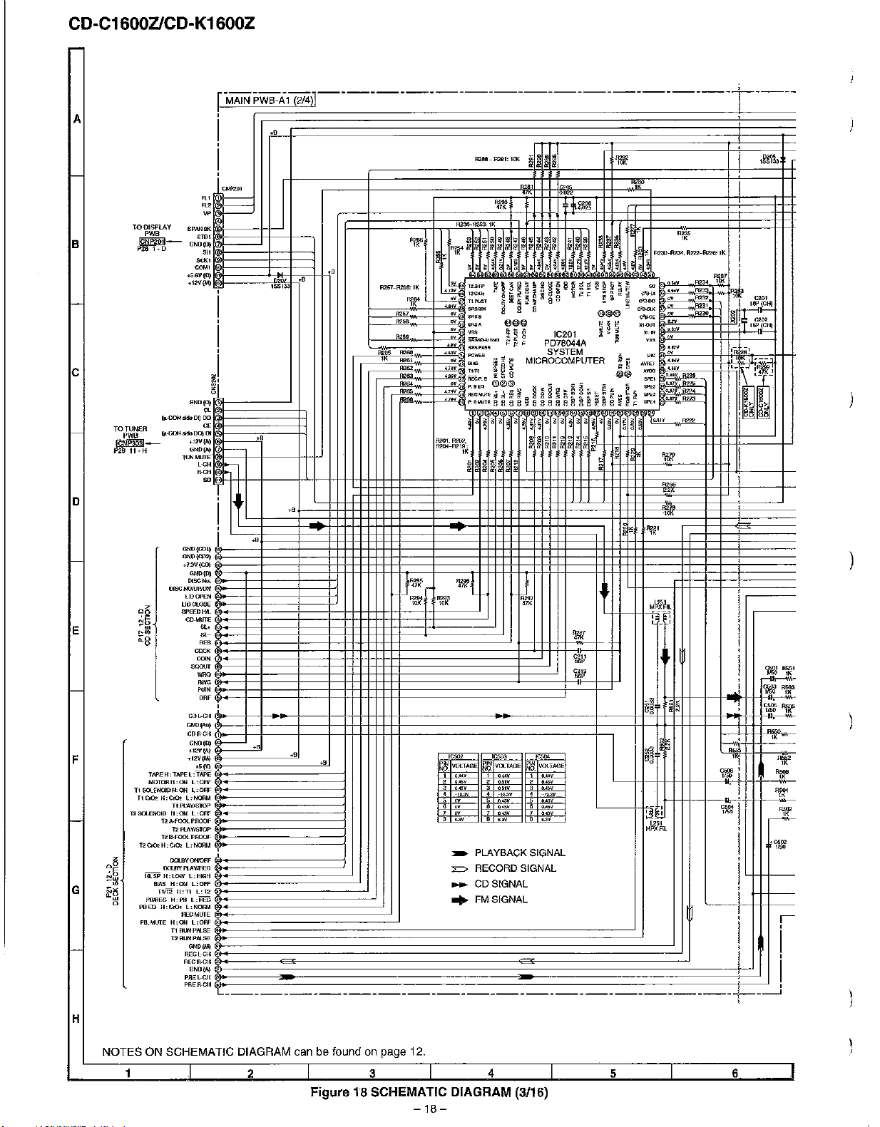
CD-C1600ZlCD-K1600Z
A
rODISPLAY
,we
B
ICNP2011-
1'261-D
c
GND(DJ
Q
POO
(p..coH<iIIo>ogoo
C£
(pAXlHsiOODO)lJI
.12V(A)
GND(AI
.w
'"
TOTLINER
ICNPsosl_
P2911-H
D
i-------
..
.,,,
"
...,'v
..
""'
"""
..
""'
..
""'
=
~'"
-"
,
.'
,-
.J
:~J
i~~
'000
GNDlCOI)
GNO{cmj
+7.:1V(CD)
GND(D)
"'"~
IJISGNOIIJPlDN
lIDOPEN
UOClOSE
SPEEDWL
CP-MurIO
E
F
TAPEH:TAPEL:TAPE 1
11
SOL~~~~~
11
Cr02
T2SOLENOID
12Cr02
iii:SP
PBEQ
I1II\S
f'8Il1EG
G
Q.
Q-
'ffi
=
~
~
~
~
~"
0"'
GNOjAu) 2
CDIl·CCI 1
w,.wM=9=Fff~~~nms
.':!V(M)
.5M
~~~:
H:CIO> L:NOOM 5
TI
PLAY/SlOP 6
fl:ON
l:OFF
T2f\.FOOLPflOOF 8
12
PLWISTOP
12
B.FOOL
PIlOOF 1
H;
C/O,
L;
NOHM
-~
OOUIyptAYIRI;G
H:lOW
L:HIGH
H:ON
L:OFF
TIm
H:n
L:T2
H:PS
L:I1EG
H:Gc02
L:NOIlM
REGMUTE
n
ALWPALSE
T2l1unpALSE
000,",
REGl-GH
RECR·GI-l
GND(A.)
PREL_Cll
PREJt.GII
.0
C601
R501
~
.J
W&
Rwr
I
"'§
~o
~~
~..
-:
C505
'\150
IlfIr
Ilf'O
+8
+8
~
F,;;;'~="':==II;;;~~1"'==j
0.""
1
O.<-IV
1
....
~
VOLTAGE
~W~.~~I'~~'III1S~'~.~=i'~~E
~
~
~
4
ov
ov
7
OV
~
~
=
-
~~:~~~~
,"-'v
4 ,
•.
w 4
5
0......
8
0.,""
1
0.......
B
..
:IV
PLAYBACK SIGNAL ,
RECORD SIGNAL
CD SIGNAL
FMSIGNAL I
5....,v
6
7
8
0A5"
..
6.OV
v
'2':"
.,v
~ci
,C504
~_
I 1/50 !/f
1.251
1.11')(
m ,
W,O'
C!i06 ;
"''''j
•
i
l,
I
!
14-++--
I
1
R562
~
1K
',~
IK
~
.--
i
i
i
----------------------------------------------------~-~
H
NOTES
ON SCHEMATIC DIAGRAM can be found on page 12.
1
2
Figure 18 SCHEMATIC DIAGRAM (3/16)
3 4
-18
-
5
6
----:-----------------------------------!
=,
~~
"
1234, R222_R226:
,~
'i'.II
..
..
,=
=,
-
=
"
..
~
..
..
~.
~.
m=
~
=
1SS133
lK
,
FJ2#
Q",
19P(Cllj
!Jl+
Q.
~
15P(CH)
'~iil
,
,
-
'-~'W1:
i~
'~-
i
i.<
6>-
:6
,;,
it>
<l
':;',mm
~PAN
~IOO
,~
""'
Jl
ELECTOR ll2<l1
(;201 ISS13.3
0.01
10208,
11SS133,
'
___
I
182L\lI;1X)ll
"w
mk,
3.31<
e"
..
c
,
!@
POWERiUNE
"iR"
.,.
~
Sf'
GDGND
GDGND 02
,.
PROTtSp
fjW
~'~
•
.2'V~
0202
~n
,
..
RB..AViRJN
MllTB'SYS
.m
Dl
~7:JV
C
GND(M)
R211
0.2" 100
KT~GR
MUTE
-=-
,
,
,
~
..
~"
"
~OU
'lm.i
00022
c.,
~'l
=
:.r!~
.....
LV~
UNVlN2
5.3OV
LToUT
'''''"
lVRIN
."""
l~ST
,.39\1
LVROUf
103"
VDO
....vVr.1
'.m'R\fRO(JT .
5"'.
RTEST
....v"""IN
.~'"
RTOUT
."""
R1NVIN2
~
"'..
gRFS
~
~a:
..
a:
i~'
=--
~oo
IliI
,~
I
j
-...
""'
,
i
" "
~~k'
IJ¥
~7~l:~
~
A
,
~~1
=~
1150
lK
=-
lJSl1
lK
,
'""
~"
"
-
"
-
"
~
"
ow
,,,.
f
,-
i
,
~
P22
I
,
35~~gl~S6~~8~6~a~8~il~~~~6t~~g
L.3
":;:"w~_'''Dg'''g~~DrL~rL''rL
'.u.v
~~
'NCov
•l2....
v s.nv
NC
.v
LI
~.<V
vss
oV
Qw
DI
(p.·CQN.HIo DO)
~
'"
AVss
~.
"
NC
....
R2
W
NC
n,v
it'
..
..
..
ov
v
_ '.J9'I RV",r
z 0 - a 8 - N 8 - N 3 -
~~d~~I~B.~~~k~~~~~~-
",a:..a:
a: ..
~I~;
flm
~Jr
~~
a"
".
----M>
,
gS
8
00
~tJi
is
" <
t-E
..
:l:c:l:
OzO
..:.,,<i:
~ ~
P22
1-E
<:613 G515
<:617
C519 C521
'frl'
tIi
'"
--,--,--,--,--,--,--,--,--,--,US
LC75394E
PROCESSOR
~a:
~~~
.o-rtMi
9 8 8 5 4 I
..
";~~LL";i!:lll~LL
IC501
AUDIO
~
.."'.."'.."'..
~~~~i
---------------------
PISS
~
R274
'"
1lf~5
coNTIPOSISTOR
~.
,~
~.
'"
o.~7
s.IV
~~~
p~
~
,
=
"m
~~
~~.
~'f
01W7
"l"Je
~"
47/25
=
18313:l
,
=
~~PD
~,.
m.
,W
,w
,.
~
"
,.
~.
,ro
,.
MrZ£mcf
,.
'IDI
.=
=
,~
•
IfJr
,~
,~
'!III
-
..
il!\1*
~4
~
•
=
0,0027*
~
~"
I~L
~w
185133
~
~"
!Uty
5
0
,
..
~
..
=
I'''''
~f
R~~8
0>
---------------------
~gs
000
Oz,
a:"~
P22
1-0
~
.~
'!Ill
~
~"
~"
CD-C1600ZlCD-K1600Z
W.
q:;,
<5.6V(D)
I
,
,~
=,
4.7/SQ
'"
R456
4.1/
r=:
C::
r------
,
,
,
"
,
,
,
~__~r::~
~
..
.=
~»
~
-I--
~
....
"
~
..
If..tRjss
IC502
~
45fi~~.2150
1C504
IC503
BA4558
=
-
=,
,~
~
=.
~,
.~
I~~
""'-•,/,;i(:04
~
b~l
In~
Iii.,;
I~t
~~"""""'IC503
~33
GNOIII)
~&OO
~~
SPPAOJ
SPRELW
~
~,
lINEMUTJ::
.'l'.V(MJ
COGN[)(lJ1)
CDGN[)(OO)
..7.3V(00)
GND{M)
~"'"
..12V(II)
_15V
,
l
•
,
OUl(L)
=
...
''''
GND(A1
.12V(A}-
PASS
""""
~"
~"
SRSINfl
J
-----------
,
INtll
,
="
~"'"
.,2V(A}
INCA)
OUf(fI)
.
GNIJ(D)
•
""
I--I~~;r--
L_::"'-_
OPE
,!Il1l,
2.215l1 lOOK
"'i\UI"'"
lJF33
:t
MP.
~1s3
,=
"'i\t
1~33
C65~.t
2
;
....
AMP.
1~~h
~t
,.~
.215O
..
TOSRS
_ c s
'TOKA
AMP.
~W!f
tW~
J~
~~a
JI'Ml
-,
SPE·4
J\\l'Ii
lilt'!
J!lI!
.
PSI
~
eNS
~:
'"
pw
-
!'
"
!'
'-H
'WB
3.A
~Ei
____
_J
:
,
:
I
,
,
,
I
__
-,7
,,-8
--"-9
__
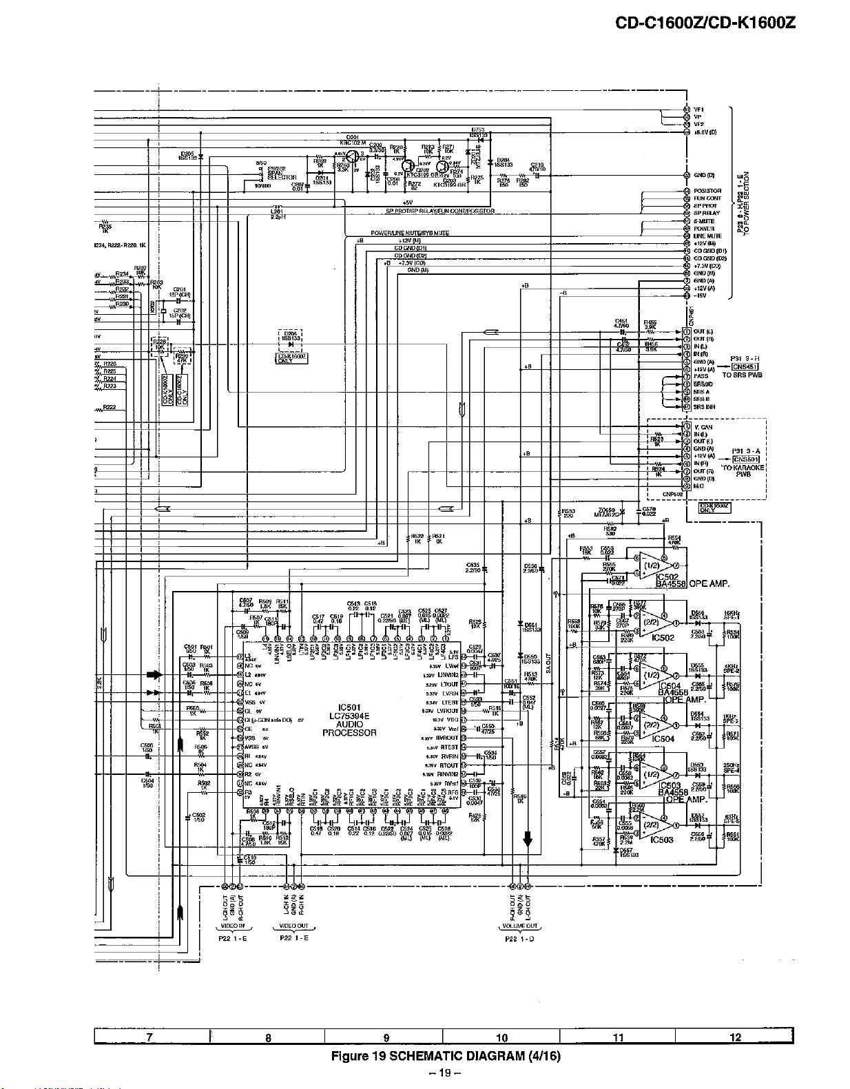
Figure 19 SCHEMATIC DIAGRAM (4/16)
I 10 1
-19
-
11
12
CD-C1600ZlCD-K1600Z
A
B
~
PLAYBACK SIGNAL ::c:> RECORD SIGNAL i
___________________________________
I
,
--1 _
i
,
,
ICD01
HA12134A
RWl
~y
~---M-~-r_-,~,!:/;~.,-+-:w..,--J-~.·'oI.
~I'~Jr"
NR
~i'._llV"'--~1£~1~+::::;1=_~-==
(112)
~
0.'"'1
rif.><""~,£~l~+'~'l·,h""'-r--+-r-'
~5
I
'~i~~:J
0.1<'/
2 IN
~
1fN
-=-=-t'~~,,;;:;"c'",:"S!!T~·*'+-_+--+_+--+;;;_I_+___,--r--l--t:
l-
ODIC
KRC107
t-+-
••
"'~H!'~"'~'",.
VROO4
::J
22K(B)
c
~
~
L--!
, ,
D.12V
~lwl~====='="='="'="==:"~======1--___J----~----___J-1-----
o
lei01: PLAYBACK AND RECORDI
PLAYBACK AMP.
p~~;I'~~
QOO7!2l?'f\3
a~a
M
Kfle,
~~
<"'"
1t-"o
Hi~- .
__
,
"'
17V
0=
1W
~
7 M
!~~3~
~~
COO4
~"=l'l
47DP
/-;o,;;;,.;;-+-"~l
+=:--I-::=r'~
',',n
',~,
IK
CD52
COlO
1150
1/50
L---E~-----+_------ri'~----
.~~,~!
a.Brn
"l
~
g~~
•.
'_;;~'o"",.",.~
cHo
COO;/f,O
330P
~
,~_~
u.>U.<
6
amH
,~r-J~r~
'l'I'
lK
-l(.!
§!<o
...
~
IC001
~212)
'~I~
O~
~~~~~k3
L--'---";;;"'+-Ht1I-~O~
r
il;1-+,---f------+-H't1----!-
~""
0-2tV
<--...J
8
",'N
.',P.,','
"~I'li
~W<'
CO,_,,',4
R,~k2
~,
:ill>.
1
~
+-I-+_
~;
~~
-,
~
~
~
~:
..
'lEft
>o.~'~.~.
c--+-'.i'~---l-
COle
10116 0
\Wt
i
i
)
E
R112
,
W
2SG=SE
F
"00
n",-v
~.~K
n<I":lW~.~O~
~&1~SE
""
0109
KTAl266GR
G
L-----------------------------------i----
H
NOTES ON SCHEMATIC DIAGRAM canbefound on page 12.
1 2 3 4
'~.~
'"
Figure20SCHEMATICDIAGRAM (5/16)
,,~
tQK~w~8
omclD
ci
Uo
" .
Cl09
0.0220."""
Rl14
10K
Rlla
"
t
W 3
2
0110
KRG104M
<:IV
-20-
Gl14
~JJ~
-
GIla
47/16
R120
~
PH EO{CJ02} o ,
.,
,.'"
0."""
o ,
KA%\1,lM
•
gM~
,,~
'00'
KRG104M t W
,,~
,~
,,~
~Jo~
•.
~.~~
'i\f~
o.~
,,~
'"
0114
~~:
.~"'
PHEQ{GrO»
,,~
''"
,.[
=
00
r
o~
5 6
HI
SPEEO';;;
I I
Hi9''''.t----
,
I
CD-C1600ZlCD-K1600Z
i
'--~---------------------------------l
:
RD'4
,~
~lt
I
~5
J
8~
,
,
,
f
~,
,
,
~
"
:
I
I
,
P.BMlfTlNG
W.b.~~1l
e,'0.'"
"<
~
o~
8.
•
<
8§
~
o~
<N
e~
UK
~~~
,~
CD46
ADIS
"'
ooro
lSS1~3
"W'
I~
DoLBY
PLAYIREC
DOLBYONJOFF
L:OFF
G01S
,~.
~
;~;~i~=~;;;;;;;~~~=~:~~~==========================~pElMUTEH;O/f
'"
C017
10/16
,--
~~kl
~~Il
,w
,
CO'6
10116
HI.
SP
ALe
GHD
~"
'\'
"'
4.'
....
iC142
47125
em
~\t
"
7
8
Figure
9 I
21
SCHEMATIC DIAGRAM (6/16)
-ZJ
-
10
1
__
....l.11!.-
~12,--
__

CD-C1600ZlCD-K1600Z
A
:--iAPE1
I
PWB-E1
B
TAPEIPLAYSW
SWU
1-
TAPE.MECHANISM-l
[ PWB·E2 I
c
till.
TAPE2
PLAYSW
SWE2
SOls8:'?ID 0
o
P19100H{
TO
SECTION
E
P19
TOMAlN
SECTION R
F
MAIN
g.H
VIOEO
VIOEOO
{
VlllEG'AU
'"~
VWEOIAUX
O~
,.
G
R-C
~
C<
II
,
,
"""
,,~
NOlA)
"~
No(A)
~"
.~
~
,
G
I I
IJ.FP B-FOOL PROOF
SWE3
S~4
1-'
~=~=~=~
,
CHIN
,.,
""
"~,
-
"
~
"'"
~
,
, BA4558F +
'"
""
=
~
]
;33
;li?"'
~~*
~*
~4
1
~='
• R592
lK
KTG3~GR
,~
,
1
,
l
MAl!,
~wt
,Wi!,
0.022
R6!l1
..
....
.~~'~~
PW".-Al
MECHANISMI
i
~"
PLAY/STOP
RUN
p~:
GND
~OO
C!O>
I
' .J
.,
,
+.
rnw
4.7/50
~~
!~~
OPE AMP
IC681
2:>[50
R6B3
lOOK
v~
*~fiIl4
~OOK
22150 I CBll8 58K
K~M
~
:"'V
=.
2.:>150
rnm
.=
" I
.l:~"
Om"
:~W~
lK
~
.".
~liR'R~~
3
R6B6
R688
18K
331{
""'"
lBOP
(212)-
lC681 •
(4!4fl
_12.1V
~~
."V
-II
______________________________
,...---------------------
,
I
,
!
~,
-
mJE~DI
,
"
=ce
~""
TtSOLEOOIDO
,,~
"""
T!
RUNPAl.SE
.,
Tt
PLAY/STOP
,
."
I
~tf
~oo
,~
J~Ill)
,
-
~J\kmGR
~
DRIVER
MOffiR
,
I
~
.'
T2
....
FOl1PIlCXlF
,
-
"""
T2P1..AVIsTOP
.,
•
T2RUNPALSE
T2B-FOQPllOQF
TIlSOlENOIDO
'"
~~
R~l
,.""
R
l~
CC97
(l.Q22
.=
,~
-
=
IH:<l •
'1!Iif'
GND(A)
'0'
-
~~
rn"
~,
""'
"
..
FM
..
~
,=
=
~II
"~
'jjii'
18813:1
mw~
11fd~
KT?!WsV
Ilfdoas
~02'¥"
WOO
~~
,~
10
1121'1)
0"
1~~:b
'¥."uv~lfoff
I(f~W¥\y
DllIl'ER
O~R
PvAI27,'J'
1~~
I,;
"'
tJYfg'lW)
~"
'"'
~
I
BUFFERAMP.
lC902
NJM4565M
\'!ll~
~
rn.
,0>
IMl.)
,.." -
!!!ii
=,
.~
(~,
'M"
" 'lI'
1'1""
,0><
""'
,A~'v
~'"'
~,~.v
KTC3199
00
..
-
'iJ!I
KT~GA
=~
.~
(~,
rn"
8:tt~1
W,M
~~
WJP
<lll'"
IC902
SIGNAL
.rl;io.ov
"""':"~
~
\i.~
(212)
1
+~2.,"
-----------~-----
,~"
0.-
~
O~
~3i1~G
~lf
1fI.2U
"l"ok'
~"
.~
.,
=,
t,?,,!6
'00'
~.11
~
?f
=
1?,15
~
~
.~
-
~
DR
rnlf
'iJ!I
-
"
=
-
""""'"
=ce
~"
,~
'f:'~
!'jl
lfJ.l
~,
OII~B1BA
o.1\'~1
"'
lmll
,~
=1
"'
oW
~
2SG2117BA
"'
I
I
,
I
i
i
,
I
,
,
"IJlR'
l?if
, ,
,
,
I
,
,
!'=
I
i
r
1
,
i
i
!
!
I
,
I
,
l.._-<
,
,
,
,
.
,
.
,
,
,
,
,
,
r
,
)
)
H
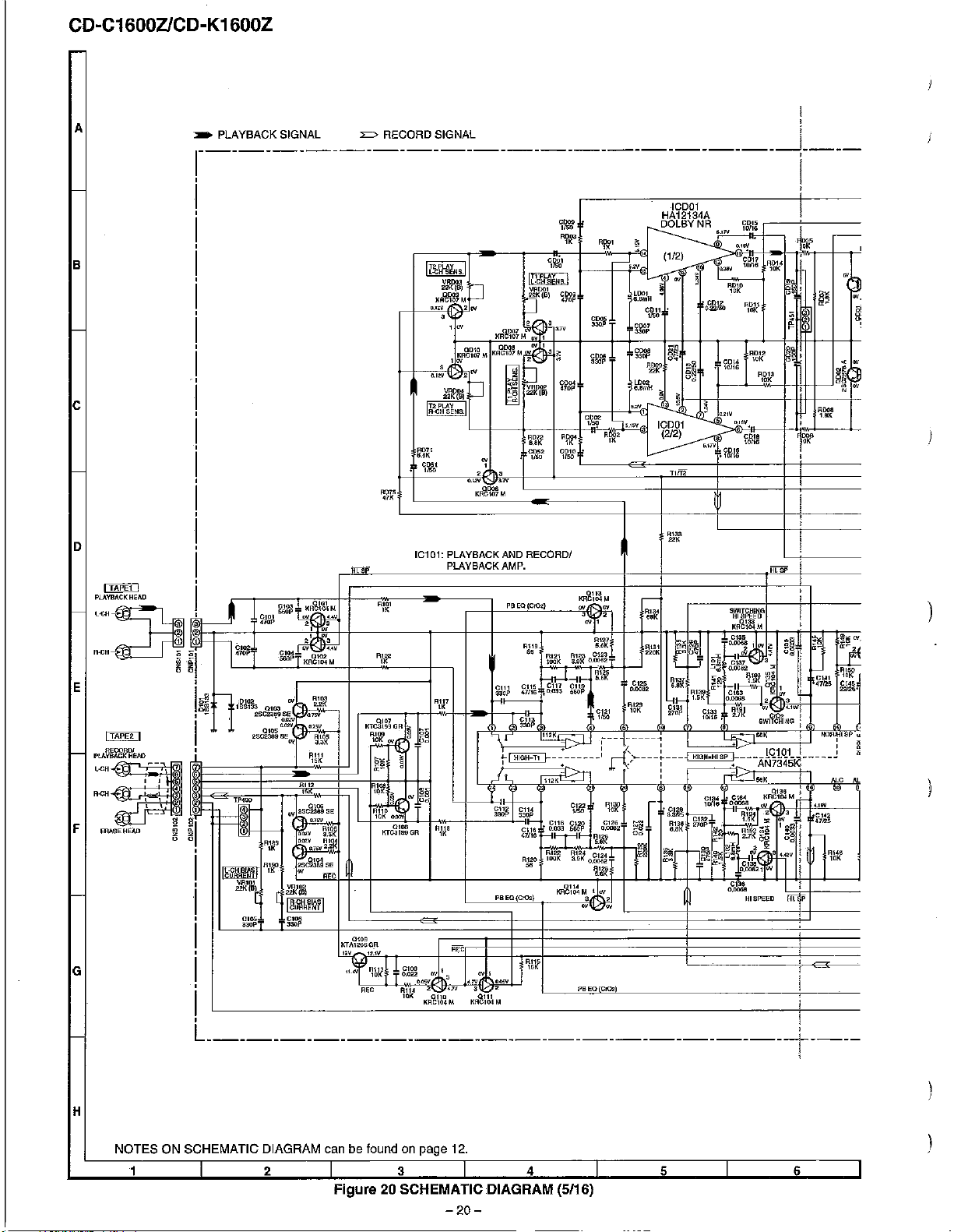
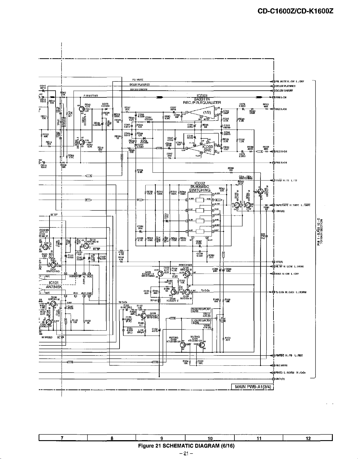
NOTESONSCHEMATIC DIAGRAM
canbefound on page 12.
2 3 4 5 6
Figure22SCHEMATIC
-22-
DIAGRAM
(7/16)

CD-C1600ZlCD-K1600Z
---- i 1
--I
- i
'----~
,
HI.SP H: lOWL:HIGHT
o.F"~
2SC2B18A
P24
TO
POWEAAMP.
eWB
:)·F
~
Pi9
12-B
TO
MAIN
SECTION
7
8
9
1
10
1
__
...J1
...
1
1~2_==:J
Figure 23 SCHEMATIC DIAGRAM (8/16)
-23-

CD-C1600ZlCD-K1600Z
A
B
c
D
,
i
,
,
,
,
I
I
,
I
I
i
!
,
;
,
I
,
I
,
,
,
om
I(~l)
o~,
(fill
R928
..,
- -
GNSa~-~l
"""1f-
E
F
G
~~
o.
1
P23
12-E
TO
MAIN
PWB
-
- - -
,
,
,
D802-D805:
,~,
!
.
,
,
i
r3
,w,
'"
0=
"
"
0
"
t-0!
L----
P2312·F
I
cNsaotl_
TO
MAIN
PWB
CNP801
I
,
I
,
,
,
4
't-
,
:
i
,
I
I
,
I
I
,
I
I
,
I
H
NOTESONSCHEMATIC DIAGRAM can be found on page 12.
2 3 4
Figure24SCHEMATIC DIAGRAM (9/16)
5 6
-24-

CD-C1600ZlCD-K1600Z
---~-----------------------I
'M
SIGNAL!
+--,--1 1
>eg97,
f~W'
41/50 56K
I
I "If
t.,"
~~
I
I(flQ
en!
{fill
,
ALSOI
-
;---~--:
,
,
,
,
,+-:--~~~-+'-1~
,
,-'
,
,
,
,
,
~
~
185133
1-+---t-----------t(~1
i
'
80001
-@ L-CH
m~1Wlt
"~
';
I
I
! C922 •
I{~Q
,
I
'I
~(,,',",
'"
,
R928
4.7
I
\
I
,
~B
I---+---i-+--+-----N;~---'--""~~,oo--\<D'~I
~~W
~kl
!--+=o-I-~>c_~=+-''-''j1:J
~
KTC~~§gGR~~J~
o
,,""'OV
.'71V~
_W
3.3K
A2~6
0996
188133
I
1~~~~3
f&~
+'
ZD999
MTZJ5.6B
Ar~4:~
II
t-::----J
~
12\1
~
,uv
ov
~
KTC~~~GR
I '
,,~
l
~I
~
--~------------------------'
12-F
~
NPWB
CNPBOl
g~~~~'oo~(''''''~~.,,~.~.
R934 AELAY
l00(ll2W)
,
1----------------------
,
!
&1--
1
! I BR1D2Jll2 I
,
<
I
+6
!I:'m
•
l
'
,
,
,
,
,
,
I
,
I
I
,
I
,
,
•
t:.-
,
,
, MTZJ5.1B
I
,
I
,
I
-----
0001
II
I(
'1+ I,
I(
LL
0&02-0&16 : ,
~~
RBOI
'"
-:-
.-.-_J..-
ww
Rl.204F
Dll!I3 0004
coo,
47150
•
CB07
,~,
,~,
II
I,
I.
~'"
"00
coo,
O.1J41
(~I
=,
0.047
~"
•
C~
0.047
{ML}
C~
_00
ca04
0.041
(ML)
-,
41!SO
MTZJ2700
,~
2.2K
."
-,
000'
2S81370
R~ba?6R
ALS01
1-------;
,
,
,
,
:
1-"
, ,
, ' ,
~!
0820
1SS133
0508
RU04A
~~
o.
O~
RLI04A
D8'iiI
RL104A
2!~
R~J.1A
dmiW)
~
---P~~A---:==-------J
TANSFOAMER
___~l___
,
,
,
' ,
I I
'1--++
':
:
I
,
, ,
,
,
_____
I
~
:n,f~50V:
----
-h
-or
.i
o.
'00.
u
'00'
T2AL250V
,~
T2A
L250V
1~
--------J-----
220V
1~~
SWBOI
sVE'&"h'folk
'~"OO'~
I:
i!
LBQ!'i.EB...,S_UPPLY
PWB:~.L
~
R810
"!.4{1!Wl
_____________________
,-~~~~~~~~················1····-
I~~I
0994
' M
rl2
~
I'
I
1
4'ii\8
2SA562Y
I'
!n
GND
4
HPR·CH
RELAY
1
1
,
1
,
,
I
I
,
I
>0-
,
I
,~
~
!
I
,
__.:
MOO'
AIROOOLING
FAN
__
..:.7
---lB~
__
1 9 I
Figure25SCHEMATIC DIAGRAM (10/16)
-25-
10
1~_-,1u..1
-",12~_-,

CD-C1600ZlCD-K1600Z
---------------------------------------+----
A
ICNS1ll1
•
.;>
~
'.
.~
~
~~
~
~~
••
"-
"~
~
•
Rro.
,
!
I•••
'iTf
~a:
~~
:<
"
~
oj<
'.
~
'lOi'
,~
"~
8~
~~
"
$'
"
~
~!
~
1i
",,,
•
~
~
•
•
,
,
~2~~~
•
i
E
""
1
1150
F
2~
~
lSS133
KR~~M
,
,
,
.~
-
C710
.=
em
I
~~
,
1
i
.1"
1
.L
l
.m
!
K~4
G115
~"
.~
:______________
G
I,
'K::::E
I I
~ER
'-
~
~:!-L~
1 I
J
~~
~.w ~1:
~R
r~
~~
~7:J
I
R.PlAy
r-:;"
~~
I
PA1JSE
~1~
~;J~J~
r~~::
,--o:=:J
I
IfN
nEw
.-
rlJ,!
I
~Ir
I
ArM
i
.k
i
1
;".
r~lf
'&
1
H
NOTES ON SCHEMATIC DIAGRAM can be found on page 12.
1 2 3 4
---------------------------------+----
Figure 26 SCHEMATIC DIAGRAM (11/16)
5 6
-26-

CD-C1600ZlCD-K1600Z
."
~
..
~
."
~
."
~
..
""
"
'1'.11
~\II
,~
~U<'
I
""
'"
I
,,~
'"
"«
'"
~ll~~~
,
I
i
:
,
I
i
~
I
1
:
!
,l.
;
I
!
KLS
,
,
,
I
""-,
,
I
RlOO-R7OS;
,m
1K
Ar~S
AA,"
.~
AA721
.~
ill"
='"
I--- I---
I
, :
, ,
~
-
,
, ,
---
-,
,
__
..!,7~
l!.8
__
I 9 1 10 1
Figure27SCHEMATIC DIAGRAM (12/16)
-27-
__
--!.!11
__
..L..
__
..!.<12"--
__

CD-C1600ZlCD-K1600Z
A
IC303L=1
PIN
VOLTAGE
NO.
B
c
D
E
1 2.06V
2 5.01V
3 'l.01V
4 2.06V
5
OV
6 S.09V
7 S.09V
8 2.84V
9 S.otV
11
3.85V
12
3.85V
1 3.95V
14
1.18V
1
1.19V
16
2.05V
17
2.29V
1 2.52V
19
OV
20
OAGV
21
2.2V
22
2.2V
2
S.OtV
24
3,48V
AN,\fJk1
IC302
PIN
VOLTAGE I 1 2 3 II-
NO. I
1
2.521,1
~ ~~
4
01,1
~
::~~v
7
F
0.161,1
8
12.1V
9
3.851,1
10
3.951,/
11
5.11,1
12
2.381,1
13
01,1
14
01,1
15
01,1
16
2.481,1
-----
r
1
I T
1\
'Itr
....
I
~tfT~?"~~
" 7 28C2878 B 1K R324
NN;.:,'..
17
'----S-0-30-,-1
-,
ANTENNA
--l
TERMINAL ,..I
I
l,1
• 188133
!-'--"-!@!-'-J
1;:;:1
I~I
JmI-:J.
,J
J
I
I
I
I
.
I'
1188133 RTiD t
~~
ca03
.-r-...
0.022
--v'
8.g1~I
8.3~~
ISW20Sc.1
~
. . I
D301
188133 I
~J
8W1
0302
I",M"W-,-"o",s",c",1
- . I I I 68K 18P 18P C336
BAND
~tTSESR
BFT01
CT01
18PovlOY
LIt-
~J8~
«.
Cil
1-1
,r
ClL
>
~
RT02 (UJ)
0303
33K;K;
---
----:3:::
22K
0305 I
188133 I I , r
T
R320
0316
asc.!
ICTa1
TA7358AP
FM FRONT END
rf
~3)
OT02
V.Ul
CT04
0.0010
:+- 0
I
l!:i
I
T304 KV1236Z23F
SW,
~
~N!'
II
. I
1~~6
0306
13..Q:}.
R321
S.6K
G31S
0.1
10K
rT]Q..8.,
I
~~'
=lj;
T.,20.l.,
l:&l:
1~:t....1
J£O.§
~
-~'-~
~
~....
OV
It--
••
n,W
_5 6
......
~rYli;
~jO?
1
>---~b~
..-(1)
GTOS....
6.ap
RTD3
~
ti:
22 eno 47K G390
UJ'~
~
l 3
C316
0.1
0315
188133
R322
S.6K
C31~=
0.022;
G3l9
O~$22
TC304
I>
MIX
01,1
~
0307
2SC2878 B
ovr
!la306
(UJ)
B.A
01,1
CT11
7
I OV\; R327
TC305 ,vl,
1 VD301-2 100K
I R323 C334 C335
(lr~)
it
t':l I I I .;%i VDT01-B 3 3 3
....
IFMIFI
.I!.01
.
~,
-fif:L~.O~
~
~
~~
i RT04
~
~
2=:
VD302-B
Q T
ov
309
R3i2::;:o
hov
lV\. 0309
R314
Tl'R328
10K
VD302·A
KV1236Z23F
JJ:l.32~
~~~
fl00K
In~
5.6K 18S133
ov
0317
(CH)
1Ci@
'oft
8)
RTOB
11.61,1
10
CT12 CT16
~3~
~:
L I
GTl3
47
3.9P IUJ
RTDS
---
CSO?
3SK
470P
047
...,..
1SS133
~
:R313
D313
188133
D314
188133
C321
0.0039
R326
1K
R330
C34
vee
~~
9
b~
~+
=1=.
10/16 1 1
"<L-
;:::
NO
0
C\I~
~b~8
--------
-
----r
----
I
R31l
100K
C309
330P
C3l2
0.022
I
.--~"'-fI
~~
:!:Oo
;J;
R325
56K
<D
co
+
~
~
"'9
1/50
J.J.
:r...
ij:o
~&l
~ ~
l3
;Z'~~:;(
!
~r
R343 R342
47K 47K
R33-....
470
~ ~
,"341
47K
+-++;j--+-"'~
fl)~8
01,1
8~~2_8_~~2;;~2'18!V
~
1~~
I
[~=!~t~~f~§~~E~
.........
4.7K I
0365
~R~~
'"~
r~J;:
TEl:
351
+B
I
I
,
:2
C382
°ts
,l5P
CH
+8
C342
0.022
-
'------
R382
-
c!t-
4.5
--11-
_
A::
150
12P
(CH;
~'
8
.:
I
i
G
I
I
,
H
NOTES ON SCHEMATIC DIAGRAM can be found on page 12.
1 2 3 4
Figure28SCHEMATIC DIAGRAM (13/16)
5
-28-
I
6

CD-C1600ZlCD-K1600Z
----r-----------------LTuNERPws:-cl
-
-I-
-I-
-
,
FM
I
..
,
~17
L-
"u.,,.!i4:!1'~
""!,-!!~-_-'?!'L~O!.g:"2..!I'~,'-----.I\"p..l'~'L"'i'ffi!>'!.i(,'!14'---!!:t,,"'!L,
!
I
,
C 02
~
~·F3~tf~c~3~5Qotb,~-:;_;,;;:_~3i
f
11'",=,1
•
L:
[J::J
~Ol-OZO
t:i~
l!S13
lB-
t?o-..,~~iE
C'?
.....
lLX
-::5;:~!:!:
u:~
"'l°-'2
0.022
(\J
oiiio~
..C352
~
x
~1-(9
~z
?tiS
'3'
"
~
:;:;l
I 0
--c-
10/16 IAMIFI 0
~
I
-'T351 1
~
::a;3:~:::<1-
~ ~go~5
:::<
<r:
!:!:
~z
4"5
v \
R352
27K
=
2
¢
8.5g~
-g
n 2.2K
~-"'-_+_
R3S0
2.7K
X351
456kHz
CaB?
.. 1/50
~u-
I§~
0
~
a
liii
6 7 8 9
gf
!1i
o
'"' ,.
~
~ci
~
ro
B!
LL
gj~o
"-~~~o~
R393
1K
C3B5
0.01
G3B7
0.022 L351
100~H
SIGNAL
MW/SW1/SW2 SIGNAL
~~
C373
~;;
0.022 R364
..
~:rgK!__t='i~r5~7J=~~~~36~~ttM~U~T~I=N=G~~~~:t==h
ffi~
~T"""
~o
8~
0
~ 5~ ~
~
~
~:;;
I;;~
'~"
....
,-,.J'"
...
me
,~
..-
:MCiJ"
a:(\J__()
oro
0"
R376
1K
..
C72 R362
1750
~~""
d;0 0
~
t::
~ ~
~
~
'!I1V
C359
foT
U~cr",~
~o
(0..-
+-:!:""
~g
~o
00
~~~5
R377
47K
3.3KovEC3199
r-
~
I~
~~ov
:1i
~llL
",
~I
1O~
2c?
l? 0
b'!!2
0
....
+
R363
2.2K
0353
":H',O""""V'!tI>=-_-h
r::JI
ov
I~
~~.65V
~
R354
3.9K
L352 Z0351 G396
100~H
MTZJ5.1B
GR
Ra6S
10K
RSS?
C37S
1K
3.3/50
~~~8
G395
GR
G376
0.022
A391
Ra66
10K
1QO/10
390
Q354
~q.1~§l
0.022
~§l\
X352
4.5MHz
C1J
®
(3
R39?
1K
-
,
I+B
,
C384
0.001
i I
-
-----+----------------------------
__
...!.7
--'s!!.-
__
R373
R374
R371
R372
R3?1
-
R374:
1K
-
I 9 I 10 1
Figure 29 SCHEMATIC DIAGRAM (14/16)
,-29
-
0351
188133
+B
~3233-jj!,
~2~3~4~5~6~7~8~9~'~O~'~,
e-dg~og~~oo@
__
~
~
E;j~~..Jd:
':j:Gffj
I
eNS202
TOMA1NPWB
....J1U,.1
I
P1B1-0
Z
F!
J-
-
...J.l12,--_....J

:I:
Gl
."
m
c
C'l
.,
l>
o
."
.c"
<:
Cil
Co>
0
III
0
:c
m
;;:
'»-
0-
'"
-l
,0
C
s;:
G)
~IA
;;:
~
~
01
~
-
S
z
~
m
(f)
o
z
(f)
o
I
m
;;:
~
o
'"
"
t;
OJ
l>
;;:
"
!!l
0-
'"
is
c
is.
I'"
g
-0
TO
MAIN
I
CNP451
P1912-C
PWB
r-------
SRS
£i
~
'"
!"
r-----------------'
I ' ,
,
I
,
~
I r
CIl
Z R453 26rNA:J, 0469
U~
OUT
(l)
1
OUT
(R)
IN
(l)
3
IN
(A) 4
GND(A)
5
+12V(A) 6
PASS 7
SRSJ:lD
lra-\I--
SRS
A 9
SRSB~
SRSINH @
,
I
,
I
~
+6
-i
__
0:02V
~2
0466 R449 1
KRC10~~
ov
Q4S9 _
KRC107M
_
3~2
4.4V
\l::Cl'0.01
11
ov
oo~
~I
R452
4.7K
~
1.5K
....
'11.4V'~-
ov
3 ",rJ<::
~r'1
:>
'"
R454
2.B6V
R457,
12Kjs.6GV
2.2K
2.2K KTC3199
2.6'5'1
~
--;;\
Do
5.~
Q467
V}£;..6.'5V
\lKRA1Q7
~
W'Q460
~~RC107M~~
OV
11.4V
3'\.1
~.I2
~
a
....
KRC107~tf':\2
~
",'"Tl
KTC3199
GR
5.7V
5.7V
Q46B
I
GR
R458
"I
12K
KT~~J3
12.15V
M
g~
~J9
f::~
a':~
~
j:!l<:
~~
~~
E:<:\i
<O~•f'-~.
10;:.;
(5~
R451
10K
Y
1,.4V ",8 0 a;I.o
:>
~
10-
8
C)..-
--------------------,
Rf~B
+B
en·
a::~"'!'"
Cf)
~
:g~
T"'!'f'-
o~
ci
D451
155133
~~
t:iii5
R465
1K
A466
1K'
en
.....
10
~
cr:
en~::
+6
R479 R484
22K
R480
47K
0460
0.47/50.
.
~
Z~
ZI$
~~
-,,,,
0 0lod
:::ii;
....
z5
~
;T;i
zl~
c...",
c...",
ll)
T
R482
33K
R483::J
100K
1;5K
C461
0.0047 _ _ _ _ _ _ 4.7K 1.5
:kR481
_f).9K
(5!:;t
~e
~
g:~
if...,:
3 4 5 6 7 S 9 1 1 1 1
ci 0.47n
4 1
~i3 ~ia
:::;$
Lri
Ood
u
" "
~~
C\I~
on~
0", 0",
0",
::
~ ~
C\I~
16~
(2;;;
(5gj
~g
(5~
$;?~,,"'&
ONOOOOf'-g
d d d
+ C467
:3~
~$
0.,;
U.,;
~ ~
lSLri
B",
~
~ ~
ffi-;;;
(50
ci
d
~%
1
6 ..
FCoJ1
~:rf
l50
(MI.)
:::is
'§i3
U",
>..;
<0$
:;I~
0",
(I)",
oc...
(5r:o:>
*81
~~
19
16
5$ 5$
01";
5
0l~
CflLri
C\lg
r:o:>g
f'-{;'J
~;;;:
lS"<
O~
0...
R490
0454
.or
2.2150
R468
100r;
t--
(i 1
0:$
~E;r1~:39V
01";
U'"
C!l
~
~~ ~~
0"; 0";
-v~
~f'-
O~
S;~!..r
II]
F-"'I~
"<;f"
1l:!~
0",
-iI
t4t,
C475
Pr~2[
)
+B
I~~~.
~ ~:£~
it~~...
0476
~E-
> >:>> >
~ ~ ~S~;l
6
14
~
08
~
1 X 0~A B
f-
>
w I I :J:
rd
0 2 Y 3 1
en
1 2 3 4 5 6 7 S
:> :> :>
~::'i
ll!
'" '"'"'"'"'"
:;
~
~
8
Ii
..-
R49~
R492
4.7K
31
:>
lll.ll!
0>6
a!;?
---l
RSOO
6.8K
~!
~
11
9
~
tll
gJ
:;
> >
:>
:>
:>~
~
co co
...
"l
..-
h
...
en
o
~
C
,
...
"
en
~
'01
'0>
-
I
,
I ',2 I I
_________________________________________________________________
---l
-

CD-C1600ZlCD-K1600Z
CD-K1600Z
A
B
c
D
E
ONLY
~
"
•
~
:e~:::",
(3~
9
§
§
<
1O~
~
•
~
~
~1!l
~;-;
~
9
~
,
U
<
~
~
>
~
~
~
"~
~ci
~
ll.
0:
::2.,....~
",0""
"'<0
Q
2
tll
,
~
'"
'"
"0
u_
"'
~
"0
~
~.
~
~
•
~
L
,
£
. .
~
~
z
~
~
"
w
£
>
0,
""
irlg
~c
~+~>
~
z
"
•
~
~
i
~
M
,
, z
~
"
8
~
~
>
•
-
I~
-
i3§
oW
•
§!~
~~
U~
~i'li
0
u
~
~~
~
~
~
~
i
°
"
°
"
~
~
~
~
~ ~
~!§
I~
~~
u•
••
•
u
g
0
z
U
"~
u.
""
~~
2>
!8g
.-
§~
ue
-"
13~'
Uo
F
~~
G
L
__
H
NOTES ON SCHEMATIC DIAGRAM canbefoundonpage 12.
1 2 3 4
s~
l3~
h
1
"~
~~
Figure31SCHEMATIC DIAGRAM (16116)
~~
g'
~
~~
~
~~
~11!
is;
Ol'
~
UN
*~
t 0
~~
.~~
gg
~~
"'"
~§!.'!.
::;'"
..
."
-----"-*H~*--------
-31-
~!
.'
>.
~
"~
1-<'
:3~
~
i~
g!i
§~
U
o
h
LJ
00
~::i1
gill
.-
~~
0
•
Ii:!
~
> 0
~!i
§3
Uo
"
",
~.
"~
~:
5
~I
;:,
~I
~,
~I
,
6

CD-C1600ZlCD-K1600Z
A
I MAIN PWB-Al I
B
C
0
E
FMlAM(KHz) I
TO
POWER
AMPPWB
ICNS90s1
P37
11-C
VIDEO
InR
VIDEO
OUT
L-CH
INPUT
VIDEOIAUX
R<>H
L-CH
VIDEOIAUX
OUT
R-CH
SW202
SPAN
SELECTOR
10OJ[~
IN
'0'
:'
,
"
F
G
H
The numbers
Oto
mare waveform numbers shown
2
,
,
,
,
,
ICNP802!
P3710·B
TOP~AMP
in
page 39.
3 4 5 6
Figure 32 WIRING OF P.W.BOARD
-32-
)
)
(1m

CD-C1600ZlCD-K1600Z
TO
___
nun....
CNS801
:'.1
G'
'
-'
G •
-'
GY
~
DISPLAYPWB
ICNS701 I
P343-A
TO
POWP~J'UPPl
-->-- ICNP801 I
P366-C
Y
TO
KARA.OKE
PWB
ICNS601 I
P351-E
,---------------------------------
, ,
, ,
, ,
, ,
, ,
, ,
, ,
,
, ,
, ,
, ,
, ,
, ,
, ,
,
, ,
, ,
, ,
,
................
P383-G
I FWM21
TOTAPE2
MECHANiSM
PWB
_J
..
,
,
,
.
__
ICNS102!
P385-H
!QI&§.~A~
....!7:""",
I
CNS101
I
P3S
5-F
IQ.
IAE'~..HEAlL
82.-
P38
3-E
_n~ICNPM11
TOTAPE1
MECHANISM
PWB
FWM1
~
__
1 9 1 10 1
Figure 33 WIRING OF P,W,BOARD
-33-
(217)
ISRS PWB-A2 I
1!.!-1
....!J12'--
__

CD·C1600ZlCD·K1600Z
A
B
c
P3312-B
TOMAINPWB
I CNP2011
+
o
)
E
F
G
H ISWITCH PWB-B2!
1
2 3 4
Figure 34 WIRINGOFP.W.BOARD
-34-
)
IDISPLAY PWB-B11
5 6
(317)

CD-C1600ZlCD-K1600Z
ICD-K1600Z ONLY1----n
,
,
,
,
,
,
,
,
,
,
,
,
,
TO
MAIN
,
,
,
,
,
,
,
,
,
,
,
PWB
I
CNP502!-'-
P33
11-0
+
ICNP2021
P324-A
TO
MAIN
PWB
unun
---------
--------------
IKARAOKE PWB-H I
---
- ---- -
------ - - n - n - u__- -
---
------~
, ,
~
- - - .!
VR603
ECHO
VOLUME
~-----------------------------------------------------------------------------------------
7
8
VR602
MIC2
VOLUME
9 10
VR601
MIC1
VOLUME
I_;
';::::::i
I I ' ,
~-------'
Figure 35 WIRING OF P.W.BOARD
-35
-
" ,
----~-'
._~--------~_'
\;======:t
J602 J501
MIC:::
(417)
~-
MIC1
11
'
12

CD-C1600ZlCD-K1600Z
A
B
c
)
,
"
,
,
,-
,
,
,
,
,
,
D
,
,
,
,
,
)
E
,
,
,
,
,
,
,
,
,
,
,
,
,
,
>-
,
,
F
.J
, ,
1=::===========::1
SWB01
VOLTAGE
G
AC
POWER
SUPPLY
(240)
AC
1101127/220f230·240V
SO/60Hz
H
1
2
Figure 36 WIRING OF P.W.BOARD
CORD
3 4
-36
-
SELECTOR
IPOWER SUPPLY PWB-D21
5 6
(517)

MOO'
AIR COOLING FAN
CD-C1600ZlCD-K1600Z
,
ltj
J901
J 1 HEADPHONES
----------------------
um
'"-,
J
IHEAD PHONE PWB-D31
TO
MAIN
ICNP903!
P321-D
PWB
-----.-
r:Y-=~----,
CNSOO1
n ,
,
----'----
L LEFT..J S0901
SPEAKER
7 8 I 9 I 10 I
---
......
--
Figure 37 WIRINGOFP.W.BOARD
LRIGHT..J
TERMINALS
(6/7)---'-'---
-37-
IPOWER AMP
11
PWB-D11
12

CD-C1600ZlCD-K1600Z
'w..
MECHAUP
A
CNS5
"
"
"
"
____
•
~
•
,
M
•
,
,
,
0'
,
,
"
P33
B-A
I CNP5
1...0(
rOMAIN
PWB
B
ISENSOR PWB-E I
8W2
OPENfClOSE
0
SLIDE MOTOR
M2
M'
LOADING
MOlOR TfT,UP/DOWN
M'
ICD MOTOR PWB-F I
"
P:l25-A
I
CNP3!-e:
__
C
o
rOMAIN
P337-A
~-e:----
TO MAIN
P326-A
I CNP2
TOMAINPWB
n
PWB
CNS3A CNS3B
g[~:!<]~q~z_
Qtl1-
!~
~__~~~~~
~
. 4
CNS1A
~~
•
PWB
!--e~-
~
0'
~
~
"'
Y.
\
f~I1i
\
~
~
Eti~1_B_J
" ,
~
~
n_n_un_uu~1
eNS1B
____
:
,
\~n
un unun
IPICKUP UNIT I
•
r=r.;====r=;;h
o
o
.,
1000001
I' •
~Io
0 0 0 0 0 0
01
SPIN
M1
MOTOR
)
E
SOLENOID
SOll
TAPE 1 MECHANISM
PWB-E1
F
G
TAPE 2 MECHANISM
PWB-E2
Ipaa
10-61
TO
MAIN
PWB
t
P3310·F
ICNPM2!
rOMAIN
PWB
~
fLLL.l.!.Ll...LH
1
FWM2
P33
ICNP1011._
TO
MAIN
P337-H
ICNP11121
TO MAIN
lAPEl
PLAYBACKHEAD(57)
8 - H
f-:'~-!E;:<'-l--",J
POO
PWB
2 B
1 p
CNS101
RECORD/PLAYBACK!
ERASE HEAD(58)
BK
"e
.....
8l
@
TAPE2
YL
RD
WH
\
H
1
2 3 4 5 6
Figure
38 WIRINGOFP.W.BOARD
-3B-
(717)

o
,m,
a.sov
F,E
Sm,
5.0V
DRF
WAVEFORMS OF CD CIRCUIT
STOP---PLAY
FOGUS-
BERCH
v-
I
3
1
a.5ms
10.QV
JP+
a.5ms
10.QV
Jp.
O.5ms
0.50 V
JP
O.5ms
t.DDV
TE
CD-C1600ZlCD-K1600Z
IAI~~_
...
I~"IJI
"
I I
r\
'~
..
"
IW
6)
0
0
e
0
0
0
e
0
0
G
e
Q
0
a.5m3
t.DaV
HF
a.5ms
5.QV
HFI
a.5m3
5.QV
TES
a.5ms
1.00 v
HF
a.slllS
5.DV
HFI
a.5ms
5.QV
TES
50m3
10.QY
JP+
50ms
10.QV
Jp.
50m3
a.sov
JP
50m3
t.DDV
TE
a.5ms
10.0 V
JP+
O.5ms
10.QV
Jp.
a.5ms
(J.SOV
JP
a.5ms
t.aav
TE
I
II
r
I 1 I I
I
..Il
A,W.
~
rVmyVII
fi
I I I I
r "[ 1"11'1
l;.
VW"
mv
j'
PLAY
NORMAL DISC
TNO=Ol
PLAY
TCD·712 (140mm)
TNO",01
I;'
""I
PLAY
TCD-712
CUE
CIY
20ms
I 1.00 V
SPD
m
20ms
2.00
V
CLV+
REVIEW
50m3
CIY
t.DaV
SPD
50m
m
,
2.0DV
CLY+
CUE
I
I
tI!\
~omv
'I':'
SlD
.I
....
'"
1
tr:\
0.55
W
lOOmV
SID
"
0
e
e
0
50ms
10.0V
JP+
50m3
10.QV
Jp.
50ms
a.sov
JP
50ms
1.0DV
TE
REVIEW
,
I
jl
"r
I
I I I I
II
-39-
-
1

CD-C1600ZlCD-K1600Z
TROUBLESHOOTING (CD SECTION)
When the CD does not function
When
the CD section
the
objective lens,and
the
following items. .
Remove
"Track
Before
Turn
Gently
Do
Is
IC201
Is
specific
When
In
the
cabinet
skipping
allempting
the
power
clean
the
not
touch
the
from
5 V
till
pin
55
when
there following
state?
theCDmechanismismoved
other
states:
does
not
operate
check
the
and
follow
the troubleshooting instructions.
and/ornoTOC(TableOfContents)
any
adjustment
off.
lens
with a lens cleaning tissue and a smail
lens
with
the
bare hand.
OV
down
pulse
(approx.
the
turntableisrotating?
Yes
voltage
inputonthe
5V
playback
make
300
"lJlr
"
IC201
up:
OV
When
operation.
certain
ms)
input
pin56in
the
objective lensofthe optical
When
this section
maybecausedbybuildupof
that
the
lens is clean. If not, clean itasmentioned below."
amount
into
the
the
No
No
pickup
is dirty,this section
does
not operate even after the
dust
other
of isopropyl alcohol.
1 Check the
SW1.
"'
Check the MECHAUPSW
56tothe
SW1
MECHAUPSW.
foreign
and
mailer
the wiring from the
and
may
not operate.Clean
above
stepistaken,check
on the
laser
IC201
the wiring from
pickuplens.
pin55to
the
IC201
the
I
Pinl
Check IC2 pin40
periphery.
and41092,
I IC201 defective.
Is
there
following
specific
state?
When
theCDmechanismismoved
In
other
states:
IsLoutput
IsLoutput
skip
switchispressed?
from
from
voltage
5V
the
the
inputonthe
IC2
pin
IC2
pin40during
•
41?
Yes
093,
Yes
Yes
Yes
Yes
and
up:
094
IC201
OV
SEC
and the
I
pin56in
when
the
the
disc
No
No
No
"I
Check
the
56tothe MECHAUPSW.
-:
Check the wiring from
Check the wiring at IC2
MECHAUPSW
the
IC2
093
I
pin40and 094.
iC2 defective.
I
and
the
pin41to
~OK
defective.
lOK
wiring trom the
the
093
base.
I
I
IC201
)
Pinl
)
I
I
.Is4V
above?
Check
output
turntable
from
the
motor
092
and
emitter
Yes
turntable
during
operation
mechanism.
stated
No
Check 092, 093,
094
and
the
periphery.
I
I
~40~

CD-C1600ZlCD-K1600Z
Is
there
following
53,54?
Open state: Pin
Close state:
Intermediate
IsHoutputtoIC2
OPEN/CLOSE
voltage
inputinspecific
53
OV
Pin54OV
state
between
pin24or25for7seconds
keyispressed?IC91isdefective. Replace
open
Yes
Yes
state
stateofIC201
and
close
state:
when
the
pin
5V
it.
,
Is4Voutput
stated above? No
Check
The CD
between
the
loading
operating
motor
keys
IC91
pins3and7during
Yes
(M1)
and
don't
work.
Yes
the
loading
operation
mechanism.
Check the OPEN CLOSE SW and the wiring from the IC201 pin I
No I53,54 tothe OPEN CLOSE SW.
.I
Check
the
No
wiringofthe
IC2
pins38and
39,
IC91
pins1and
i OK
IC2 defective.
I
~I
Check the periphery of IC91.
I IC91 defective.
~OK
I
I
9.
I
I
Check the CD, DSP, power supply, and 16.93 MHz clock,
and
reset
terminal.
Yes
of
Check the waveform
Seeifthe
If
microcomputer
::··~~'C:·i!llIc_···.:s:=:
1
~~.~~"'"-.3'.~
I
Check
Playback
Does
pick-upisin
the
items
the
canbeperformed
the
pick-up
mentioned
Focus-HF
SCK, SO (DATA) andSI(COMM).
Yes
the
pick-upinPICKUPINSW
Yes
above
are
OK,
check
IC201:.
system.
withoutadisc.
Yes
moveupand
No
down
twice?
the
main
position.
0.5s
0.50
V
IC1
@FD
0.5s
0.50V
IC10TE
I
1/
V
I
Focus
search
Yes
OK
1\
Figure
Focus
earch
is
s
/
performed
two
times
when
play
operation
done
without
disc.
1
2
is
41
Doesthe output waveform of
Fig.41?
Check the
Check the microcomputer data
and (53)CE.
. .
IC1
(50)(CLK) line, 4MHz.
IC1
No
(16)(FD) match thatshown
...
on
pins (51)(CL), (52)(DAT)
in
-41-
Yes
Check
the
area
around
IC5~CNP2.

CD-C1600ZlCD·K1600Z
Is the Focus servo active? (Can you hear itworking?)
Yes
Does the DRF signal change from
Is
HF
waveform normal (see the Fig.42-1 ,2)?
Check the tracking system.
Yes
Yes
ilL
n to "H"?
HF
1.0V/DIV
O.5flSec/DIV(DC)
(When playing
back
the
disc)
~
l":" I"U
/
Figure
~
42-1
No
No
No
0.55
i.00V
ICI@FD
0.55
IC2@CLV
0.05
10.QV
10.OV
ICI
@DRF
0.05
2.0DV
IC10TE
Check the laser diode driver.
Check the area around IC1(16) - (21) (focus servo circuit).
If
the
discisnot turning,
DRF should not changeto"H". Yes
Level is abnormal.
is
Waveform
unstable:
f---+--e-+--1-+-+---+-+--+-+---j case of
the
Check
the
spin system.
Check the periphery of
IC1
pins41and 42.
Check the spin system.
Waveform
normal play-
back
In
t=EljEt~~~~~~~~~
1==Jo,=F=9=,p
Figure 42-2
rCheck waveform
The waveform shown
Fig. 42-3 appears, and nodisc state appears soon.
Play is possible in
--.
TEST mode.
Data cannot
)
of
ICI
pin 7
(TE)l
be
5ms
1.00 V
1
IC
5ms
5.0V
ICl
in
r 1 Although IL
Yes
read.
TE
0
@DRF
~--+-_+----+-_I--4---ILL--I----1_-+----I"
"I
Yes
Tracking servo
inoperative.
play is impossible.
Is
l .
Yes
Ip
Posslble'l
Yes
Check the VCO-PLL system,
Check the periphery of IC
Yes
1 pin 8 to pin 15, and IC 5
to
CNP2.
Normal jump
and
the program top
cannotbereached.
i.s
impeded,
I
" Check the periphery I
Yes
of
IC 1 pin 14.
Figure 42-3
-42-
)

I
Play
operationisperformed
I
The
turntable rotates a little.
without
Ves
No
disc.
CD-C1600ZlCD-K1600Z
I
The
spin
driver
Ves
circuitisnormal.
l
~T~h"etltuJrrrrnt~a~b~le~f~ai~ls~t~o-"ro~t~at~e'..'o~r-"ro~t~a~te",s-,a~t~h~ig~h-,s~p"ee:'d~'
L
I
Play
operationisperformed
I
AlthoughHFwaveformisnormal,
0.55
1.00V
IC2@PDO
0.55
1.00V
IC2@FD
when
Ves
disc
TOe
exits.
data
If!"
cannotberead.
."
J
ly~"'11
Ves
I
Ves
1
Stop
-->
Play
AsVCO
freque-
ncy
lockedat4.32
M Hz,
of
PDQ
2
and
zes.
is
voltage
rises
stabili-
Check
the
'I
IC2 pin 13 and pin 14, IC5 to CNP3.
Check PDO waveform (Fig. 43).
I Check the
peripheryofIC1
Abnormal
IC1
pins 43 and 44, IC2 pins 3, 5, 7, 10, and 11. I
pins23to
27,
pin
39, and
pin
40, I
I
Check IC 2 pin 58 (EFLG).
Check IC3 pins
Check IC
1,
7.
501
and POWER AMPiC90.
FIgure 43
Ves
Abnamal
I~
I
3
No
-43-
Usually,
secorless.
the
numberofpulsesofflawless
discis100 pulsesl

CD-C1600ZlCD-K1600Z
FUNCTION TABLE OF IC
IC2 VHiLC78625E-1 :Servo/Signal Control (1/2)
Pin No.
1 DEFI
2 TAl Input
3
4 VVSS
5
6
7
8 VSS
9"
10 EFMO
11
12" TEST2
13,
15 VIP
16" FOCS Output Focus servo ON/OFF output terminal. Focus servo ON:
17" FST
18
19 HFL Input Track detection signal input terminal. Schmidt input.
20 TES Input Tracking error signal input terminal. Schmidt input.
21" PCK Output
22" FSEQ
23
24 TGL Output Output terminal for track!ng gain selection. Gain increased:
25" THLD
26" TEST3 Input Input terminal for test. Pull-down resistor is built in.
27 VSS
28,29
30"
31" TEST4 Input Input terminal for test. Pull-down resistor is built in.
32" EMPH Output
33" LRCKO
34" DFORO Output R channel data output.
35" DFOLO
36" DACKO Output Bit clock output.
37" TST10 Output
38
39
40
41
42" LRSY Output Output for ROMXA
43"
44" ROMXA Output
45"
this
In
Terminal
PDO Output
ISET Input
VVDD
FR
EFMO
EFMIN Input
14
CLV+, CLV·
FSZ Input
TOFF
JP+,
Jp.
DEMO Input Sounding function inputterminal forset adjusting process. Pull-down resistor is built in.
ASDACKIPO
ASDFIN/P1 InpuVOutput
ASDEPC/P2
ASLRCKlP3 InpuVOutput
CK2
C2F Output C2 flag output
unit,
the
terminal
Input/Output
Name
Input
-
- Powerterminal for built-in veo. Usually 5V.
Input
-
Output For slice level control EFM signal inversion outputterminal.
Output
Input
Outout Output terminal for spindle servo control. When
Output
Output Focus start pulse output terminal. Open drain output.
Output
Output Tracking OFF outputterminal.
Output
-
Output Output terminal for track jump. When
Output
Output
InpuUOutput Input for antishock
InpuUOutput
Output
with
asterisk
mark
Defect detection signal (DEF) input terminal. (It is set to "L" when
For PLL
Digital system grounding terminaL Usually
Input terminal for test. Pull-down resistor built in.
"H", deceleration is set. Three-value outputwith command is enabled.
Rough servo/phase control automatic selection monitor output terminal.
Rough servo: "H" Phase control mode:
Focus error zero cross signal input terminal. (It is set to
Clock monitor terminal for EFM data playback. Phase lock mode: 4.3218 MHz.
Sync signal detection output terminal. When sync signal detected from EFM signal coincides
with intrinsically generated sync signal: "H"
Tracking hold output terminal.
Digital system power terminal. Usually 5V.
acceleration is set. In case
inner periphery jump is performed, acceleration is set. In case of outer periphery jump
deceleration is set. 3-value output with command is enabled.
Deemphasis monitor output terminal. Deemphasis disc playback:
Digital filter output
Output terminal for test. Usually
General-use port
when antishock is not
applied.
nis
Input terminal fortest. Pull-down resistor is built in.
Phase comparison outputterminal for external veo control.
Grounding terminal for built-in
Resistor connecting terminal for current adjustmentofPOD output.
For veo frequency range adjustment.
EFM signal output terminal.
EMF signal input terminal.
of
inner periphery jump deceleration is set. When JP- is "H" and
Word clock output.
L channel data output.
"lIIoutput.
Bit clock input.
UR
channel data input.
(PO-3)
Built-in deemphasis filter ON/OFF selection terminal.
(ON: "H" OFF: "L")
Word clock input.
UR
clock output.
Bit clock output.
(in
RESET mode)
Interpolation data output. ROM data output.
(in RESET mode)
(open)
terminal
whichisnot
Function
veo.
Usually
av.
ClV+
"l"
Jp+
is "H" and outer periphery
connectedtothe
not
used)
OV.
is "H", acceleration is set. When
"l"
"l"
when not used)
"l"
JumpISpertormed,
uH"
Polarity inversion clock output.
(in
CK2CON mode)
(in
ROMXA mode)
outside.
elV-
is
)
-44-

CD-C1600ZlCD-K1600Z
IC2 VHiLC78625E-1"Servo/Signal
Pin No. Terminal Name
46"
47 LVDD
48 LCHP Output
49 LCHN Output L channel N outputterminal.
50 LVSS
51
52
53
54 RVDD
55" MUTER
56 DOUT
5?"
58" EFLG
59"
60"
61" SBCK
62"
63
64 RWC
65 SQOUT
66
67 CQCK
68 RES
69" TST11
70"
71"
72
73"
74 TEST5
75
76
77"
78
79
80
In
this
MUTEL Output
RVSS
RCHN Output
RCHP Output
SBSY Output
PW Output Sub-code
SFSY Output
FSX Output
WRQ
COIN
LASER Output
16M
4.2M
CONT
CS
XVSS
XIN
XOUT Output
XVDD
TEST1
unit,
the
terminal
"
Input/Output
-
-
-
-
Output
Output
Output
Input
Output Sub-code Q output standby output terminal.
Input
Output
Input Terminal to input command from microcomputer.
Input Terminal to input command input intake clockorsub-code fetching clockfrom SQOUT.
Input
Output
Output 16.9344
Output
Output
Input
Input
-
Input
-
Input Input terminal for test. Pull-down resistor is built in.
with
asterisk
Control
For 1 bit DAC
Digital
OUT
Sub~code
C1, C2, single
Sub-code frame sync signal output terminal. Fall when sub-code is
Sub-code read clock input terminal. Schmidt input. (It is set to
Terminal to output 7.35 kHz sync signal frequency-divided from crystal oscillation.
ReadlWrite control input terminal. Schmidt input.
Sub-code Q output terminal.
Schmidt input.
Reset input terminal. When power supply is turned on, the terminal is once
Output terminal for test. Usually
Laser ON/OFF output terminal. Control with serial
mode.
4.2336 MHz output terminal.
Spare control output terminal. Control with serial data command from microcomputer.
Inputterminal
Chip selection input terminal. Pull-down resistor is built in.
Grounding terminal
Terminal to connect 16.9344 MHz crystal oscillator. (In Normal and x2 speed playback mode)
For
the x4 speed playback system, 33.8688
Terminal to connect 16.9344 MHz crystal oscillator. (In Normal and x2 speed playback mode)
For
the x4 speed playback system, 33.8688
Power supply terminal for crystal oscillation. Usually 5V.
mark
(")is(open)
(212)
Function
L channel mute output terminal.
Power supply terminal for L c'lannel. Usually 5V.
L channel P outputterminal.
Grounding terminal for L channel.
Grounding terminal for Rchannel. Usually
R channel N output terminal.
R channel P output terminal.
Power supply terminal for R channel. Usually 5V.
R channel mute output terminal.
output terminal.
block sync signal output terminal.
and
dual correction monitor terminal.
P,Q,R,5,T, U and W output terminal.
ilL"
output.
MHz
output terminal. However, 33.8688 MHz is output only in x4 speed playback
for
test. Pull-down resistor is built in.
for
crystal oscillation. Usually
terminal
whichisnot
connectedtothe
OV.
MHz
crystal oscillator is connected.
MHz
crystal oscillator is connected.
UsuallyaV.
av.
settostandby state.
ilL
n when
not
data
command from microcomputer.
outside.
used)
set
to
"L".
-45-

CD-C1600ZlCD-K1600Z
IC701 RH-iX0149AWZZ:Microcomputer (1/2)
Port
Pin No.
1*,2*
3 P30
4
5
6
7 P34 DISC3
8*-10* P35-P37
11
12 RES RESET
13 P74
14 P75
15
16,17 CF1,CF2
18
19
20-25 AN1-AN6 KEY6-KEY1 Input
26
27
28 INT2 JOG UP
29 INT3 REMOTE Input Remote
30'
31
32,33 S2,S3
34,35 S4,S5
36 S6
37 S7
38 S8
39 S9
40 S10 3G Output
41'
42 S12 2G Output
43,44 S13,S14
45 S15
46 VDD3
47-50 S16-S19 P2-P5 Output
51
52-71
72
73-80 S40-S47
81
82
83
84
85
86
87 P02
88
89,90
91
92
In
this
umt,
Name
P16,17
P31
P32
P33 DISC2
INTO
VSS1
VDD1
ANO
AN7
INn
SO
S1
S11
VP
S20-S39
VDD4
PGO
PG1
PG2
PG3
POO
P01
P03
VSS2
P04
P05
the
termmal
Terminal
- Output
CD
CD
DISC1
-
AUTO
SPAN 9K Input
-
-
-
-
-
-
JOG DOWN
- Output
9G
8G
7G
6G
DIGIT X
5G
4G
-
1G
P1
-
- input
P6cP25
-
P26-P33 Output
F-PLAY Output
R-PLAY Output
PAUSE
REW
STOP
FF
NlDEO
(TAPE
-
TAPE
VIDEO
with
asterisk
Name
mark
Input/Output
Oulput
Output
Output
Output
Output
Output
Input
Input
Input
Input Connect
-
Input
Input Connect
Input
Input
Input
Output
Output
Output
Output
Output
Output
Output
Output
Output
Output
Input Segment
Output
Input Segment
Output
Output
Oulput
Output
Output
Output
-
Output
Output
nIS
(open)
termmal
Not
LEDisoninany
LED
LED
LED
LED
Not
Auto
Microcomputer
For
Connect
For
Connect
Operation
Destination
JOG dial DOWN signal
JOG dial UP signal
Not
FL
drive
FL
drive
FL
drive
FL
drive
FL
FL
drive
FL
drive
FL
drive
Not
FL
drive2Ggrid
FL
drive
FL
drive
FL
drive
Segment
FL
drive
FL
drive
LEDison
LEDison
LEDisoninPAUSE
LEDisoninREW
LEDisoninSTOP
LEDisoninFF
LEDisoninany
LEDisoninany
Connect
LEDisoninTAPE
LEDison in VIDEO mode.
used
isonin
is
on
when
is
on
when
is
on
when
used
mode
tuner
span
+8
GND
4.19 MHz
+8
+8
key
control
used
9G
8G
7G
6G
blank
control
5G
4G
3G
used
tG
segment
segment
segment
segment
in
in
+8
whichisnot
mode
CD
mode.
disc
disc
disc
reset
selection.
clock
input
setting
input
grid
F~PLAY
R~PLAY
mode.
mode.
mode"
mode
Function
other
thanCDmode.
exists
at DISCi.
exists
at DISC2.
exists
at DISC3.
oscillation.
port.
port
signal
mode.
mode.
mode.
mode.
other
than
other
than
mode.
connectedtothe
VIDEO
TAPE
mode.
mode.
outside.
)
)
)
-46-

CD-C1600ZlCD-K1600Z
IC701 RH-iX0149AWZZ:Microcomputer
Pin No.
93
94
95
96
97
98
99',100'
In
this unit, the terminal with asterisk
Port Name
P06
P07
SOO
SIO
SCKO
P13
P14,P15
Terminal
TUNER
/TUNER Output LEDisoninany
DATA
COM
SCK
STB
-
Name
mark
InputJOutput
Output
Output
Input
Input
Input
(')
is (open) terminal which is
-
(212)
LED
isonin
TURNER
Datatobe
senttomain
microcomputer
Command
from
microcomputer
Clock
from
main
Strobe
from
main
Not
used
Function
mode.
mode other than
TUNER
microcomputer,
main
microcomputer,
microcomputer,
microcomputer,
not
connected to the outside,
communication
communication
mode.
communication
commUnication
with
with
with
main
with
main
main
microcomputer
main
microcomputer
-47-

CD-C1600ZlCD-K1600Z
IC201 RH-iX0150AWZZ: System Microcomputer (1/2)
Pin No. Port Name Terminal
1
2 P93/FIP5
3
4 P91/FIP3
5 P90/FiP2
6 P81/FIPl CD RES Output Reset output forCDDSP
7 P80/FIPO
8 VDD
9 P27/SCKO
10 P26/S00/SB 1 CD COIN Output Serial command output
11
12 P24/BUSY
13 P23/STB
14 P22/SCK1 MAIN SCK
15 P21/S01 MAIN COM Output
16
17 RESET
18 P74 STROBE Outout
19 P73 CD PUIN
20 AVSS
21
22 P16/ANI6
23 P15/ANI5
24
25
26
27
28 P10/ANI0
29 AVDD AVDD
30 AVREF AVREF
31
32'
33 VSS VSS
34
35 X2
36 P37
37
38
39 P34ff12
40 P33ff11 SD
41
42 P31fT01 V-CANCEL
43 P30fTOO S-MUTE
44 P03/iNTP3/CI0
45 P02/1NTP2 RELAY
46
47
48 IC
49
50
51
In
this
P94/FIP6
P92/FIP4 CD MUTE Output
P25/SI0/SBO
P20/S11
ANI?
P14/ANI4 SPE5
P13/ANI3 SPE4
Pl21ANI2 SPE3
Pl1/ANI1 SPE2
P04IXT1 MIC
XT2 N.C Output
Xl Xl
P36/BUZ
P35/PCl
P32fT02
P01/1NPT1
POO/lNPTOffiO SYS STOP Input
P72
P71
P70 TAPE MOTOR
unit,
the
terminal
HI
CDH/l
CD
CD
CDRWC
- -
CDCQCK
CDSQOUT
CDWRQ
CD DRF Output CD RF level detection input RF level higherthan 2.5V: H
MAIN DAT Input
-
- -
POSISTOR Input
T1
T2RUN
SPE1
X2 Output Main clock 4.194304 MHz
C'BCE
C'B
C2B
C'B
TUN MUTE Output
L1NE-MUT
PROTECT Input
VSS
SOU
SOL2 Output Tape
with
asterisk
Name
Input/Output Function
SPEED Output
Output
Sl+
Sl-
RUN
Output
Output
Input ReadlWrite
Output
Input
Input Sub-code Q standby input for CD DSP
Output
Input
Input
Input
Input
Input
Input
Input
Input
Input
-
-
Input
-
Input
Output Tuner/preamplifier
ClK
DO
DI
Output Tuner/preamplifier
Output
Input
Input
Output
Output
Output
Output
-
Output
Output
marknis
(open)
Tape
high
speed
CD
loading
speed
CD
muting
output
CD
slide
feed
positive
CD
slipe
feed
positive
control
Positive
Serial
SubMcodeQinput
Serial
Serial
Serial
Reset
Serial
CD
Analog
clock
clock
data
data
input
strobe
pickup
power
power
output
output
output
input
inner
supply
output
periphery
supply
DetectionofPOSISTOR
Tape
mechanism1run
Tape
mechanism2run
63HzBPF
250HzBPF
1
kHz
4 kHz
16
kHz
Analog
Reference
Mic
Sub-clock
GND
Main clock 4.194304 MHz
BPF
BPF
BPF
positive
power
detection
output
spectrum
spectrum
spectrum
spectrum
spectrum
power
Input
Tuner/preamplifier
Tuner/preamplifier
Tuner
signal
detection
Tuner
muting
output
Voice
cancel
control
System
muting
output
Line
mute
output
Speaker
Speaker
Power
GND
Tape
output
relay
output
error
failure
input
connection
mechanism1plunger
mechanism2plunger
Tape
mechanism
terminal
whichisnot
control
selection
output
forCDDSP
for
for
for
for
supply
Open
C2B
C2B
C2B
C2B
motor
output
High
speed:
output
output
forCDDSP
for
CD DSPToDSP COIN
CD DSP
display
microcomputer
display
microcomputer
display
microcomputer
for
display
microcomputer
detection
for
AID
converter
voltage
pulse
input
difference
pulse
input
difference
analyzer
analyzer
analyzer
output
control
detection
connectedtothe
analyzer
analyzer
supply
for
AID
serial
serial
serial
serial
input
output
control
control
control
input
input
input
input
input
for
converter
control
control
control
control
Signal
Vocal
input
output
AID
found:
cut H
output
output
High speed: l
L
To DSP SQOUT
input
detection
detection
converter
inpuVoutput
clock
data
data
control
output
output
input
L
Relay ON: H
Occurrenceoferror:
Attraction:
Attraction:
Rotation:
outside.
L
L
L
)
output
L
-
48-

CD-C1600ZlCD-K1600Z
IC201 RH-iX0150AWZZ: System Microcomputer
Pin
No.
52
53 P127/FIP33
54 P126/FIP32
55 P125/FIP31
56 P124/FIP30
57 P123/FIP29
58 P1221FIP28 SPAN 9K
59 P1211FIP27 BEAT CUT
60 P120/FIP26 DOLBY Output
61
62 P116/FIP24 T1CROM
63 P115/FIP23 T2 PUSP Input Tape mechanism 2 sub-chassis
64 P114/FIP22
65 P113/FIP21
66 P1121FIP20 T2 CROM
67 P111/FIP19 TAPE FUN Output
68 P110/FIP18 SRS INH Output
69 P107/FIP17
70 P106/FIP16
71
72 P105/FIP15 SRS MONO Output SRS
73 P104/FIP14 SRS PASS
74 P103/FIP13 POWER
75 P102/FIP12
76
77
78
79
80
Port Name Terminal Name Input/Output
VDD VDD
CD
OPEN Input CD tray
CD
CLOSE
CD D-NO.
CD
U/D Input
FUN
MOTOR Output
P117/FIP25
VLOAD VSS
P101/FIP11
P100/FIP10 REC/P.B Output
P97/FIP9
P96/FIP8
P95/FIP7 P.B MUTE Output Tape playback muting output
T1PUSP
T2 A-FP
T2 B-FP
SRS B
SRSA
BIAS Output
T11T2
P.B
EQ
REC
MUTE Output Tape
-
Input
Input
Input
Output Tape
Input
Input
Input Tape mechanism 2 A
Input Tape mechanism B
Input
Output SRS
Output SRS
-
Output SRS control output. SRS1, 2:L Others:H
Output
Output Tape playback selection
Output Tape playback equalizer
(212)
Positive
CD
CD turntable
CD
Fun
Tuner
Dolby
Tape
Tape
Tape mechanism 2 CROM detection
Tape
SRS
GND
Set power
Tape
Tape record/playback selection
power
supply
open
position
detection
tray
close
position
mechanism
motor
drive
operation
beat
cut
mode
control
position
outputA:L
detection
detection
UP/DOWN
ON:
setting
inputSpan selection
ON:
mechanism1sub-chassis
mechanism
function
control
control
control
connection.
control
record
record
Output
output
output
output
output.
control
bias
muting
1 CROM
side
side
foolproof detection
4052
4052
4052
(for
ports
3D:H
output
control
output
output
selection
output
chucking
HOFF:
HOFF:
detection
foolproof detection input
control
control
control
8, 9
Function
input
Open end: L
inpJt
Close
end:
L
input
Pulse
count
detection
L
B:H
L
position
input
position
input
TAPE:H
and
10)
Others:L
Power ON: H Power OFF: L
Record:
T1: H
output
output
input
UP: L
9k:
H 10k: L
detection
input
CROM: H
detection
input
Record
Record
input
CROM: H
OTHER: L
H
T2:L
Playback: H
70 uS: H 120 uS: L
UP: L
UP: L
enabled: L
enabled: L
Record:
L
-49-

CD-C1600ZlCD-K1600Z
IC2 VHiLC78625E-1 :Servo/Signal Control
~
I~
EFMIN
FSEQ
CLV+
",-v-
SBCK
SBSY
SFSY
WRQ
,
""'UT
caCK
OO'N
RWC
DEA
vip
O'W
cs
,
J
"
HE
10
,
E3
t=f
l---o
w w
y t
Slice
level
control
Syns.ganeratorl
EFM
demodulalor
ClV
digital
seNoconlrolier
I
Subcode r
separation
aCRe
!JCOM
Interface
SelVoconlrolier
JrL
r
~
• •
I
I
1:
veo
oscillation
dock
, ,
clock
conlrol
0""
LCD701
uum
,
,
..
. .
VVKBJ486GKI-1
11
"
1 1
I~
Figure
50-1
~hhhi.
C1
,C2
and correction
Flag
2kX8bit
RAM
error
detection
processIng
I
Crystal type
liming
I
-
I Lavel
meier
I Peak meter
I
generator
.1,111*
BLOCK DIAGRAM OF IC
•
I
"
r---J
I Interpolation!
I
I
8Xoversampling
r
RAM
address
generator
mute
Billngual(1)
Digital
attenualor
.l
dlgUalfJlter
Bliingual(2) I
J,
1bltDAC
HU
r--
1
"
DigilalOUT
Extended
port
&
Antishock
interface
•
~
~
~
,
,",y
C"
RO"""
DOUT
ASOFNll'I
DACKO
DFOLO
DFORO
LRCKO
"
P10 B18
P11
P12
P13
P14
P15
P18 B20 B20
P17 B13 B13 B13 m
9G
P1
B15 B15 B15 B26 - - - - B28
P2
BB
P3
B1 B1 B1
P,
B16 B16 B16 B23
P5
B'
P6
B2 B2
P7
B17 B17 B17 h 1h
P8
B10
P9
B3 B3
B11 B11 B11
B'
B19
B12 B12 B12 B29
as
8G 7G 6G 5G
BB BB
B'
B1D
818
B'
B19 B19 b 1b 1b
as
B9
82
B10
B3
B18 831 2k
B4 B30
B5
B20
3G
'G
B25 B25
B2'
- - -
2.
2a
2.
•
B22
B32
;
k 1k
f
B28
,. ,.
"
2h
2h 2h
1h
2;
2;
1; 1;
2k 2k
1k 1k
2b
2b 2b
21
21
11 11
11
2m
2m
1m 1m 1m
1b
2m
2G
-
B2'
'l"
S2
1h
2;
1;
21
10
11
12
B23
822
1
2
B32
3
4
B31
5
6
830
7
B
B29
9
B28
1G
P18
P19
P20 B14 B14 B14
P21
P22
,
P23
P24
h
P25
P26
;
P27
P28
k
P29
P31
b
P32
P32
f
P33
m
B6
B21
B7
II
~
C;
(
::
)
..
..
CD
REC
ST
S1 S1 S1 S1
B6
B21 B21
B7
B6
B7
- 0 10 10
- - -
ON
-
OFF
(')PLAY
-
(')~
-
SLEEP
kH,
-
MH,
- -
B27 - - -
,
-
,
-
,
p
"
d
2,
2,
"
"
2c 2c
" "
" "
"
2,
2,
" " "
2p 2p 2p
1p 1p
20 20
'"
'" '"
2d
2d
1d
1d
Dp2
Dp1
2,
"
2c
10
2,
1p
2"
2d
1d
2,
13
14
15
~
S,
S6
S8
S3
S5
S7
SRSCO)
~
MEMORY
Il!INR
RANDOM
X-BASS
B27
S1
)
,
-
0
-
e
,
-
P
-
"
-
d
)
Figure 50·2 FL SEGMENT
-50-

CD-C1600ZlCD-K1600Z
SHARP
To
have your order filled promptly and correctly, please furnish
following information.
1.
MODEL NUMBER 2. REF.
3.
PART NO. 4. DESCRIPTION
PARTS GUIDE
"HOW
No.
*MARK: SPARE PARTS-DELIVERY SECTION
TO
ORDER
MODEL
REPLACEMENT
the
CD-C1600Z(B K)
CD-K1600Z(BK)
PARTS"
Contact
your
nearest
For locationofSHARP
Please call Toll-Free;
1-BOO-BE-SHARP
For
U.S.A.
only
SHARP
Parts Distributor to order.
Parts Distributor,
Explanation
of
Capacitors
vee. Ceramic type
VCK Ceramic type
VeT
VC··
MF Cylindrical type (wilhout lead wire)
VC"
MN
VC"
TV Square type (without lead wire)
VC••TO Square type (without lead wire)
VC"
CY Square type (without lead wire)
VC"
CZ
VC
•••••••••
If
there
arenoindications for
Semiconductor
Cylindrical type (without lead wire)
Square type (without lead wire)
J
..
The
13th character represents capacity difference.
("JII
±5%,
"C"
±O.25
type
"K"
±10%,
IIM"
±20%,
pF,
"D" ±0.5
the
electrolytic capacitors, erroris±20%.
pF,
"Z"
capacitors/resistors parts codes
Resistors
VRD Carbon-film type
VRS Carbon-film type
VRN
; Metal-film type
VR••MF Cylindrlcai type (without lead wire)
"N"
±30%,
+80-20%.)
VR••MN
VR••TV Square type (without lead wire)
VR••TQ
VR••CY
VR"
CZ
VR••"
If
carbon-film type.
•••••
there
arenoindications for other parts,
Cylindrical type (without lead wire)
Square type (without lead wire)
Square type (without lead wire)
Square type (without lead wire)
J .. The 13th character represents error.
("J"
±5%,
"F"
±1%,
"Oil
±O.5%.)
the
resistors
are
±5%
NOTE:
Parts
marked
Be
suretoreplace
with",&."
parts
are
with
important
specified
for
maintaining
ones
for
maintaining
the
safetyofthe
the
safety
set.
and
performanceofthe
set.

CD-C1600ZlCD-K1600Z
*
NO.
PART
CODE
INTEGRATED CIRCUITS
IC1
IC2
IC3
IC5
IC91 VHITA72918/-1
IC101
IC201
IC302
IC303 VHILA
IC451 VHISRS52508-1
IC453 VHIBU4052BC-1
IC501 VHILC75394E-1
IC502-504
IC601 VHIM65845FP-1
IC681
IC701 RH-IX0149AWZZ
IC901 VH18TK48805-1
IC902 VHINJM4565M-1
IC01 VHIHA12134A-1
IC02
IC03
ICT1
VHILA9240M/-1
VHILC7B625E-1
VHINJM4565D·1
VHIBA!;;920FP-1
VHIAN7345K/-1
RH-IX0150AWZZ
VHILC72131/-1
1832/1-1
VHIBA455811-1
VHIBA4558F/-1
VHIBU4066BC-1
VHIBA3311N/-1 J REC.lP.B.Equalizer Amp., 0311
VHITA7358AP-1 J
TRANSISTORS 0451
Q1
071,72
Q91
Q92
Q93
094,95
0101,102
0103-106
0107,108
0109
0110,111 VSKRC104MI/-1
0113,114 VSKRC104MII-1
0119
0121,122 VSKTC3199GR·1
0124,125
0126,127 VSKRC104MII-1
0128
0133-136
0201
0202,203
0306-309
0353,354 VSKTC3199GR-1
0360
0361-365
0458-460
0461
0463
0466
0467
0468,469
0631
0681,682 VSKTC3199GR-1
0699
0701-705
0706,707
0708
0709
0710-715
Q801
0820
0821
0822
0823
0824
0825
0826
0827
0828
0901,902
VSKTA1266GR-1
VSKTC3199GR-1
V8KTC3203Y/-1
VS2S0468-C/-1
VSKTC3203Y/-1
VSKRC1b7M/I-1
VSKRC104M/I-1
V828C2389SE-1
VSKTC3199GR-1
VSKTA1266GR-1
VSKRC104MII-1
V8KTA1271Y/-1
V82SC2236-Y
V8KRC104MII-1
VSKRC102MI/-1
V8KTC3199GR-1
V828C2878B/-1
VSKTA1266GR-1
VSKRC107MII~1
VSKRC107MII-1
V8KTC3203Y/-1
VSKRC107MII-1
VSKRC107MII-1
V8KRA107MII-1
VSKTC3199GR-1
V828C2001-L-1
VSKRA107MII-1
VSI<RC107MII-1 J
V8DTC114YKJ-1
V8KRC107MII-1
V8KTC3875GR-1
VSKTA1504Y/-1
V828B137011-1
VS2S0201211-1
VSKTC3199GR-1
VS280201211-1
VSKTC3199GR-1
VS2S02012//-1
V82SD468-C/-1
VSKRA107MII-1
V8KTC3199GR-1
VSKRC107MI/-1
VS28C2878N-1
PRICE
RANK
J AV Servo Amp.,LA9240M
BA
Servo/Signal Control,LC78625E Q995 VSKTC3199GR-1
J
J
AC
MiG
J
J
J
J
J
J
J
J
J
J
J
J
J
J
J
Amp.,NJM4565D
AR
FOGusfTracking/Spinl Slide
Driver,BA5920FP
AH
Loading Motor Driver, TA7291S
AM
Playback and Record! Playback
Amp.,AN7345K OM3,4 VSKTA1271Y/·1
BA
System Microcomputer,
llPD78044A
AP
PLL{Tune0,LC72131
AR
FM
IF OET/FM MPX.lAM IF
BL
SRS,SR85250S
AH
Function Selector, BU4052BC
AX
Audio Processor LC75394E
AD
Ope Amp.,BA4558 0101,102 VHD188133/1-1
BB
Mic Amp.,M65845FP 0201,202 VHD18S133/1-1
[CO·K1600Z Only] 0204,205 VHD1SS133/1-1
AD
Ope Amp.,BA4558F
BA
Microcompuler,IX0149AW 0:208 VHD1SS133/1-1 J
BG
Power Amp.,STK48805 [CD-K160DZ Only]
AC
Bulfer Amp.,NJM4565M
J Dolby NR,HA12134A
J
AG
Switching,BU4066BC
BA3311N
AG
FM
Front End,TA7358AP
J
AB
Silicon,PNP,KTA1266 GR 0601 VHD1S8133/1-1
J
AB
Dlgital,NPN,KTC3199 GR
J
AC
Silicon,NPN,KTC3203 Y 0698,699 VH01SS13311-1
J
AD
Silicon,NPN,2S0468 C 0701 VHDRL104NI-1
J
AC
Silicon,NPN,KTC3203 Y
J
AC
Digital,NPN,KRC107 M
J
AC
Digital,NPN,KRC104 M
AD
J
Silicon,NPN,2SC23B9 BE
J
AB
Oigital,NPN,KTC3199 GR
J
AB
SiHcon,PNP,KTA1266 GR 0808-811 VHORL104N/-1
J
AC
Digital,NPN,KRC104 M
AC
J
Oigltal,NPN,KRC104 M
J
AC
Oigilal,NPN,KRC104 M
AB
J
Oigital,NPN,KTC3199 GR
J
AC
Silicon,PNP,KTA1271 Y
J
AC
-1
Digllal,NPN,KRC104 M
J
AB
Silicon,NPN,2SC2236 Y
Digilal,NPN,KRC104 M
J
AC
J
AC
Oigital,NPN,KRC102 M
J
AB
Digital,NPN,KTC3199 GR LED701-706 VHP5N4GTN52-1
J
AC
Silicon,NPN,2SC2878B
J
AB
Digital,NPN,KTC3199 GR
J
AB
Silicon,PNP,KTA1266 GR
J
AC
Oigital,NPN,KRC1D7 M LE0718 VHPSLV312VC-1
J
AC
Oigital,NPN,KRC107 M
J
AC
Silicon,NPN,KTC3203 Y
J
AC
Digital,NPN,KRC107 M
J
AC
Digital,NPN,KRC107 M VOT1,2 VHCKOV147C/-1
J
AE
Digital,PNP,KRA107 M
J
AB
Digital,NPN,KTC3199 GR Z0201 VHEMTZJ3R9B-1
J
AB
8i1icon,NPN,2SC2001 L
J
J
J
J
J
J
[CO-K1600Z Only]
AB
Digital,NPN,KTC3199 GR
AE
Oigital,PNP,KRA107 M Z0631 VHEMTZJ5R6B-1 J
AC
Oigital,NPN,KRC107 M [CO-K1600Z Only)
AB
Digital,NPN,OTC114
AC
Oigital,NPN,KRC107 M ZD802 VHEMTZJ5R1B-1
AB
Silicon,NPN,KTC3875 GR
AB
SiIlcon,PNP,KTA1504 Y Z0821 VHEMTZJ6R2C-1
J Silicon,PNP,2SB1370
J
AD
8i1icon,NPN,2SD2012 Z0901 VHEMTZJ150A-1
J
AB
Digital,NPN,KTC3199 GR
AD
J
8i1icon,NPN,2802012
J
AB
Oigital,NPN,KTC3199 GR FILTERS
J
AD
Silicon,NPN,2SD2012
J
AD
Silicon,NPN,2S0468 C
J
AE
Oigital,PNP,KRA107 M CF302
J
AB
Digital,NPN,KTC3199 GR
J
AC
Digital,NPN,KRC107 M CF352
J
AE
8i1icon,NPN,2SC2878 A
DESCRIPTION
YK
Q901A-904A
Q903,904
Q994
0997-999
001,2
OD3-5
QM1
QM2
QMS
QT1
DIODES
D2
03,4
0207
0301-304
0305-309
0310
0312-314
0315-317
0351-353
0550-557
0705
0710-715
0753
0801
0802-805
0820
0821,822
0823
0826
0901-904
0996-999
001-3
OM1-3
DT1
LED707-710
LED711-713
LE0714-717
LE0719-724
V0301,302
Z091
Z0351
Z0352
Z0550
ZD801 VHEMTZJ2700-1 J
Z0820
Z0822
Z0999
BFT1
CF351 RFILFOO03AWZZ
NO.
*
J
J
J
J
J
J
J
J
J
J
J
J
J
J
J
J
J
J
J
J
J
J
J
J
J
J
J
J
J
J
J
J
J
J
J
J
J
J
J
J
·1
J
J
J
J
J
J
J
J
J
J
PRICE
RANK
AE
AB
AC
AB
AB
AE
AC
AB
AE
AC
AC
AC
AA
AB
AA
AA
AA
AA
AA
AA
AB
AA
AB
AA
AB
AA
AA
AA
AA
AA
AB
AA
AB
AA
AC
AB
AA
AB
AA
AA
AA
AA
AA
AA
AA
AD
AD
AD
AD
AD
AE
AS
AH
AD
AC
AC
AC
AC
AD
AA
AC
AB
AC
AB
AA
AD
AD
AD
AK
AE
DESCRIPTION
Silicon,NPN,KTC1026
Digilal,NPN,KTC3199
Silicon,PNP,2SA562 Y
Digital,NPN,KTC3199
Digital,NPN,KTC3199
Silicon,NPN,2SC2878 A
Digital,NPN,KRC107 M
Silicon,PNP,KTA1266
Silicon,PNP,KTA1273 Y
Silicon,PNP,KTA1271 Y
Digital,NPN,KRC104 M
Silicon,NPN,28C535 C
Sllicon,1 SS133
Silicon,RL104A
Silicon,1 SS133
Silicon,1 SS133
Silicon,1 SS133
Silicon,1S8133
Silicon,1 S8133
Silicon,1SS133
Silicon,lSS135
Silicon,lSS133
Silicon,1SS135
Silicon,1SS133
Silicon,1SS135
Silicon,1SS133
Silicon,1SS133
Silicon,1SS133
Silicon,1
S8133
[CO-K1600Z Only]
Silicon,1SS133
Silicon,RL104A
Silicon,1 SS133
Silicon,1 SS355
Silicon,188133
Silicon,RL204F
Silicon,RL104A
Silicon,1 SS133
8l1icon,RL104A
Silicon,1S8133
Silicon,1 SS133
Silicon,188133
Silicon,1 SS133
Sllicon,188133
Silicon,188133
Silicon,1 SS133
LED,Green,5N4GTN52
LED,Green,SLV312MC
LED,Red,SLV312VC
LEO,Green,SLV312MC
LEO,Red,8LV312VC
LEO,Green,LMKD515B
Variable Capacitance,
KV1236Z23F
Variable Capacitance,KDV147C
Zener,5.6V,MTZJ5.6B
Zener,3.9V,MTZJ3.9B
Zener,5.1V,MTZJ5.1 B
Zener,3.9V,MTZJ3.9B
Zener,6.2V,MTZJ6.2C
Zener,5.6V,MTZJ5.6B
Zener,27V,MTZJ270D
Zener,5.1V,MTZJ5.1 B
Zener,13V,MTZJ13C
Zener,6.2V,MTZJ6.2C
Zener,8.2V,MTZJ8.2C
Zener,15V,MTZJ15A
Zener,5.6V,MTZJ5.6B
FM
Band Pass Filler
FM IF,1D.7 MHz
FM IF
AMIF
PARTS
CODE
VSKTC102611-1
VSKTC3199GR-1 J
VS2SA562·Y!·1 J
VSKTC3199GR-1
VS2SC2878A!·1 J
VSKRC107MII·1
VSKTA
1266GR-1
VSKTA1273Y/-1 J
VSKRC104M//·1
V82SC535-C/-1
VH01SS13311-1
VHDRL104A1I-1
VHD1SS133/1-1
VH01SS133/1-1
VHD188135/1-1
VH01SS133//-1 J
VH01SS135/1-1
VH018S133/1-1 J
VH01SS13511-1 J
VH01S813311-1
VH01S813311-1
VH01S8133/1-1
VH01S813311-1
VHD1
S835511-1
VHD1
S81331/-1
VHDBR102J02-1 J AM 8iJicon,BR102J02
VHDRL204FII-1
VH01SS13311-1
VHORL104NI·1 J
VH01SS13311-1
VH01SS1331/-1
VH01SS13311-1
VHD1SS1331/·1 J
VHD18813311-1
VHD18S13311-1 J
VHD1 S8133/1-1
VHPSLV312MC·1 J
VHP8LV312VC-1 J
VHPSLV312MC-1
VHPLMK0515B-1
VHCKV1236Z23F J
VHEMTZJ5R6B·1 J
VHEMTZJ5R1B-1 J
VHEMTZJ3R9B-1 J
VHEMTZJ6R2C-1
VHEMTZJ130C-1
VHEMTZJ8R2C-1
VHEMTZJ5R6B-1
92LFILTF1759AT
RFILF0124AFZZ
RFlLAOOO8AWZZ
GR
GR
GR
GR
)
\
)
-1-

NO.
PART
CODE
PRICE
RANK
DESCRIPTION
*
TRANSFORMER C9
.&
T302
T303
T304
T306
T30?
T30S
T351
T80l
IT1
RCILA1064AFZZ
92LCOILA-1S8S8
RCILAOO14AWZZ
RCILB1074AFZZ
RCILBOO15AWZZ
RClLBOO14AWZZ
RClLl0011
AWZZ
RTRNP0102AWll.
RCIUOOO7AWZZ
J
ADAMAntenna
SW1
J
AF
J
AE
J AC OSC,AM
AD
J
AD
J
J
AD
J BN
J
AD
Antenna
SW2 Antenna
SW1 Oscillation
SW2 Oscillation
AMIF
Power
FM IF
COILS
L1
L101,102 RCILC0094AFZZ
L104
L201
L251 ,252 RCILL0105AFZZ
L311
L351 ,352 VP-DH101KOOOO
L353
L356
L357
L35S
L701
L901,902 RCILZ0137AFZZ
L903
LD1,2 RCILCOO94AFZZ
LT1
LT2 RCILB0045AWZZ
VP-XHR82KOOOO
VP-MK331
VP-DH2R2MOOOO
VP-YF561
VP-DH102KOOOO
VP-YF102JOOOO
VP-YF472JOOOO
VP-YF561
VP-CH1
VP-XH2R2KOOOO
RCILROO29AWZZ
KOOOO
KOOOO
KOOOO
01
KOOOO
J
J
J
J
J
J
J
J
J
J
J
J
J
J
J
J
J
ACO.82
AD
6.8mH
AB
330
AB
2.2Il
AE
MPX. Filter
560
AD
AB
100
AB
1 mH,Choke
AC
1 mH
AC
4.7mH
AD
560llH
AB
1OOIlH,Choke
AA
0.29
AB
2.2ll
AD
6.8mH
AA
FM
AD
FM Oscillation
H
1l-
Il-H,Choke
H,Choke
[lH
JlH,Choke
JlH
H,Choke
RF
VARIABLE RESISTORS
VR101
VR102 92L
VR151
VR152 92LVRS473NBMT
VR351
VR601 92LVRR1674A
VR602 92LVRR1674A J
VR603
VRD1 92L
VRD2 92L
VRD3
VRD4
VRM1
92LVRS223NBMT
VRS223NBMT
92LVRS473NBMT
RVR-M0999AFZZ
92L
VRR1674A
VRS223NBMT
VRS223NBMT
92LVRS223NBMT
92LVRS223NBMT
92LVRS332NBMT
AC
22 kohms (B),Semi-VR
J
J
J
J
J
J
J
J
J
J
J
J
[L-ch Bias Current]
22
kohms (B),Semi-VR
AC
[R-ch Bias Current]
47
kohms (B),Semi-VR
[L-ch RecJPlay Sens.]
47
kohms (B),Semi-VR
[R-ch Rec/Play Sens.]
AB
10 kohms (B),Semi-VR
[FM Mute Lebel]
20 kohms (B),Semi-VR [Mic 1]
AF
[CD-K1600Z Only] C105,106 VCKYMN1 HB331 K J
AF20kohms (B),Semi-VR [Mic 2]
[CD-K1600Z Only] C109 VCKZPA1HF223Z J
AF20kohms (B),Semi-VR [Echo]
[CD-K1600Z Only]
AC
22 kohms,{B),Semi-VR
[Tape 1 Play L-ch Sens.]
AC22kohms {B),Semi-VR
[Tape 1 Play R·ch Sens.]
22
kohms {B),Semi-VR C127 VCTYMN1
AC
[Tape 2 Play L-ch Sens.]
22 kohms (B),Semi-VR
AC
[Tape 2 Play R-ch Sens.]
3.3 kohms (B),Semi-VR
AC
[Tape Speed]
VARIABLE CAPACITORS
TC302-305
92LTO-1527AT
J
Trimmer,20pF
AF
VIBRATORS
X202 RCRSPOO03AWZZ
X3S1
X352 RCRSPOOO2AWZZ
X701
XL1
92LCRSTL1425A
RCRM-0147AFZZ
RCRM·OO08AWZZ
J
AH
J
J
AH
J
AD
J
Crystal
AF
Crystal,456 kHz
Crystal,4.5
Ceramic,4.19
AF
Ceramic;16.93
MHz
MHz
MHz
CAPACITORS
C-1
C2 RC·GZA476AF1E
C3
C4 VCKYMN1HB102K
C5,6 VCTYPA1CX333K
C7
CB
VG-"FYMN-1G-Y103K
RC-GZA104AF1 H
RC-GZA104AF1 H
RC-OZA683AFYJ
O,01-IlF,16V-
J
PeA
J
AS
47IlF,25V,Electrolytic
AB
0.1
J
J
J
J
J
IlF,50V,Electrolytic
AA
0.001 JlF,50V
AA
0.033 JlF,16V
AB
0.1 IlF,SOV,Erectrolytic
AB0.068IlF,50V,Mylar
CD-C1600ZlCD-K1600Z
NO.
C10
C11
C12
C13
C14
C15 VCTYMN1CX472K J
C16
C17 RC-GZA474AF1H J
C18
C19 RC-GZA476AF1 E J
C20
C21 RC-GZA1
C22 VCTYPA1CX103K J
C24
C25
C30
C31 VCTYBT1CX272M J
C32
C33
C34
C35
C36
C37
C3B
C39 RC-GZA474AF1H J
C40
C41,42 VCTYPA1CX473K J
C43
C44
C45
C46
C50
C61,62 RC-QZOO01AWZZ
CB3-66 VCKYMN1HB101K J
CB7,68 RC-GZA 106AF1 C J
C69,70
C71,72 RC-GZA107AF1A
C73
C81 RC-GZA105AF1H J
C91 RC-GZA476AF1E J
C92,93
C94 RC-GZA476AF1E J
C101,102 VCKYMN1 HB471K J
C103,104 VCKYMN1HB561K J
C107,108 VCKYMN1
C111-114
C115,11B
C117,118 VCTYPA1CX333K J
C119,120
C121,122 RC-GZA105AF1H J
C123-126 VCTYPA1CX822K J
C128 RC-GZA335AF1 E J
C129,130
C131,132 VCKYMN1 HB271 K J
C133,134 RCcGZA106AF1C J
C135,136 VCTYPA1CX682K J
C137,138 VCTYPA1CX822K J
C139,140
C141,142 RC-GZA476AF1 E J
C145 RC-GZA226AF1 E J
C146 RC-GZA227AF1 A J
C147
C1S0 VCOPKA2AA822J J
C151 RC-OZA273AFYJ J
C152
C155
C162 RC-OZA473AFYJ J
C163,164 VCTYPA1CX682K J
C201
C202 VCCCMN1HH150J J
C205
G-206
C207,208
C209
C210
C211,212 VCCSBT1 HL560J J
C251 ,252 VCTYMN1CX332K J
C301
PARTS
CODE
VCTYPA1CX473K
VCKYMN1HB181K
VCTYPA1CX104K
VCKYMN1H8331K
VCTYPA1CX104K
VCTYMN1CY103K
VCKYMN1HB102K
RC-GZA105AF1H
VCTYMN1CX332K J
05AFl
H J
RC-GZA105AF1 H J
VCTYMN1CY103K J
VCCSMN1HL2R2C J
VCCSMN1HL270J J
VCKYMN1HB102KJAA
VCTYPA1CX333K J M 0.033 JlF,16V
RC-GZA104AF1 H J
VCKYBT1HB221K J
RC-GZA107AF1A J
VCTYMN1CY103K
t=l.C-GZA334AF1 H J M O.331lF,50V,Electrolytic
RC-EZOO04AWZZ J
RC-GZA107
RC·GZA475AF1H J
VCTYMN1EF223Z J
VCTYPA
VCKYMN1!-J9681KJAA
VCTYMN1CY103K J
RC-GZA107AF1A J
VCKYMN1HB331K
RC·GZA476AF1C
VCKYMN1HB561K
VCKYMN1
VCTYMN1
VCTYMN1
RC-GZA47fAF1C
VCTYMN1 EF223Z J
VCCCMN1HH1BOJ J
VCTYBT1
RG-GZA4-76AFtE- J
VCTYMN1CY103K J
RC-GZA335AF1 H J
RC-GZA477AF1A
VCKYMN1HB102K
AFl
1CX1
HB102K
EF223Z
HB471K
CX332K
EF223Z
EF223Z
A J
04K
*
PRICE
RANK
J
J M
J
J M
J
J M
J
J
AA
AB
AB
AA
AA
AA
AB
AB
AA
AB
DESCRIPTION
0.047 IlF,16V
180
pF,50V
O.1IlF,16V
330
pF,50V
O.1IlF,16V
O.01IlF,16V
O.OO47IlF,16V
0.001 IlF,50V
0.47Il
,50V,EJectrolylic
F
1 J.lF,50V,Electrolytic
47llF,25V,Electrolytic
O.OO33j.lF,16V
1 Il-F,50V,Electrolytic
M 0.011l-F,16V
AB
11l-
F,50V,Electrolytic
AA
O.o11lF,16V
AB
2.2
pF,50V
AA
0.OO27Il-
AA27pF,50V
0.001 Il-F,50V
AB
0.1
IlF,50V,Electrolylic
220
AA
AB
J
AA
AA
AA
AD
AB
AB
J
AD
J
AB
J
AA
AB
AB
AB
AB
AA
AA
AA
J
AA
AA
J
AA
AB
J
AA
J M 560 pF,50V
AB
AA
J
AA
AB
M
J
AA
AB
M
AA
AA
J
AB
AB
AS
J
AA
AA
AB
J
AB
AA
AB
AA
AA18pF
AA
AA
J
AS
AA
AB
AC
J
AA
AA
AA
J
pF,50V
100 JlF,1OV,Electrolytic
0.01IlF,16V
0.47Il
F,50V,Electrolytic
0.047
llF,16V
100llF,1OV,
100 llF,10V,Electrolytic
4.7
llF
AA
AB
AA
AB
,50V,Electrolytic
0.022IlF,25V
0.1
llF,16V
100
pF,63V,Mylar
100
pF,50V
1OllF,16V,Electrolylic
680
pF,50V
100
Il-F,10V,Electrolytic
0.01
llF,16V
1 llF,50V,Electrolytic
47 llF,25V,Electrolytic
100IlF,10V,Electrolytlc
4711F,25V,Electrolytic
470
pF,50V
560
pF,50V
330
pF,50V
0.001
llF,50V
O.022Il
F,50V
330
pF,50V
4711F,16V,Electrolytic
F
0.033Il
1 JlF,50V,Eleclrolytic
0.00821lF,16V
0.022/lF,25V
3.3ll
,25V,Electrolytic
F
470
pF,50V
270 pF,50V
10J.lF,16V,Electrolytic
0.0
068
11F,16V
0.0082
J.1F,16V
0.0033IlF,16V
47IlF,25V,Electrolylic
22Il
F,25V,Electrolylic
220 JlF,10V,Electrolytic
0.022/lF,25V
0.
11F,100V,Polypropylene
0082
0.027 11F,SOV,Mylar
47IlF,16V,Electrolylic
0.022
IlF
0.047Il
F,SOV,Mylar
0.0068
J.1F,16V
(CH).50V
15pF(CH).50V
0.022
IlF
47-1lF-,25\l,Electrolytic
0.01 J.lF,16V
3.3 J.lF,50V,Electrolytic
470 /IF,1OV,Electrolytic
56
pF.50V
0.0033IlF,16V
0.OO1IlF,50V
F
,16V
Electrolytic
,16V
,25V
,25V
-2-

CD-C1600ZlCD-K1600Z
*
NO.
C303,304 VCTYMN1
C30S
CaDa
CaD? VCKZPA1HF473Z J
caoa
ca09
C3l0
C311-314
G31S,31B
G31S,319 VCTYMN1
PART
CODE
VCKZPA1HF473Z
EF223Z
VCCUMN1HJ10OJ
VCCUMN1HJ8R2D J
VCKYMN1
HB331K J
VCKYMN1HB102K J
VCTYMN1
VCTYPA1CX104K
EF223Z J
EF223Z
PRICE
RANK
J
AA
J
AA
AA
J
AA
AA
AA 330 pF,50V
AA
AA
J
AS
J
AA
C320 VCTYMN1CX182K J AA
C321 VCTYMN1CX392K J
C330
VCCUMNl
HJ8R2D J
C331 VCKZPA1HF473Z J
C334 VCCUMN1HJ18OJ J
C335
C336
C338 VCKYMN1HB102K J
C342
C343 VCCCMN1HH150J J
C349
C350,351
C352 RC-GZA106AF1C
C353,354
C355 VCCSMN1HL220J J
C356 VCKYMN1HB102K J
C357
C358
C360,361
C362
C363
C364
C365 VCTYMNOJY223N J
C366 VCKYMN1HB102K J
C367,368 RC-GZA105AF1H J AS 1 JIF,50V,Electrolytic
C370-372
C373,374 VCTYPA1CX223K J
C375
C376
C380
C361 VCCCMN1HH120J J
C382 VCCCMN1HH150J J
C384
C3B5 VCTYMN1CY103K J
C386 VCKYMN1HS331K J
C3B7
C390 VCKYMN1HB101K J
C391 RC-GZA476AF1C
C392 VCKYMN1HB102K J
C393
C394 RC-GZA476AF1C
C395 VCTYMN1EF223Z J
C396
C397 VCTYMN1EF223Z
C39B
C399 VCTYMN1EF223Z
C451,452
C453,454
C456,457 RC·GZA107AF1C
C458
C460 RC·GZA474AF1H
C461 VCTYMN1CX472K J
C462 VCFYDA1HA224J J AS
C463 RC-OZA683AFYJ
C464 RC-QZA223AFYJ
C465
C466 RC-QZA682AFYJ J
C467 RC·GZA474AF1H J
C468
C469
C470 VCKYPA1HS331K J
C471
C472
C473,474
C475
C476
VCCCMN1HH180J J
VCKYMN1HB471K
VCTYMNl
RC.GZA105AFl
VCTYMNl
VCTYMNl
RC-GZA225AFl
RC-GZA1
VCTYMNl
RC-GZA335AFl
VCTYMNl
RC·GZA1
RC·GZA105AF1H J AS
RC-GZA335AFl
VCTYMNl
RC~GZA105AF1H
VCKYBT1HB102K
VCTYMNl
RC-GZA225AFl
RC-GZAl07AFlA
RC-GZA107
RC-GZA475AF1H
RC-GZA225AF1H
RC-QZA473AFYJ
RC-GZA474AF1H
RC-QZA182AFYJ
VCFYDA
RC-GZA107AF1C
RC·GZA334AFl
RC-GZA474AF1H
VCFYDA
VCTYMNl
EF223Z J
EF223Z
EF223Z J
05AFl
EF223Z J
EF223Z J AA
06AFl
EF223Z J
EF223Z J
AF1
1HA224J J AS
1HA224J
EF223Z
C501-50B RC-GZA105AF1H
C507,508
C509,510
C511,512 VCKYMN1HB181K J
C513,514
C515,516
RC-GZA475AFl
RC-GZA105AF1 H
VCFYDA1HA224J J AS
VCFYDA
1HA124J J AS 0.12 IlF,50V,Polyester
AA
AA
AA
AA
AA
AA
J
AA
AA
AA
H J AS
AA
J
AS
J
AA
AA
AA
H
AS
J
H
AS 1 IlF,50V,Electmlytic C573,574
J
AA
H
J AS
C J AS
AA
AA
AA
H
AS
J
AA
J AS 1 llF,50V,Electmlytic
AA
AA
AA
J
AA
AA
AA
AA
J AS
AA
H J AS 2.2 JlF,50V,Electrolytic
J AS
AA
J AS 1OOIlF,10V,Eleclrolytic C618
J
AA
A
J AS
AA
J
AS
J
J
AS
AS
J
J
AS
AA
J
AA
AS 0.068
J
AS 0.02211F,50V,Mylar
J
J
AA
AA
AA
J AS
AA
AS 100 JlF,16V,Electrolytic C631
J
H
AA
J
J
AA
AS
J
AA
J
AS
J
H
AS 4.7 JlF,50V,Electrolylic
J
J AS
AA
DESCRIPTION
0.022Il
F,25V C517,518 VCFYDA1HA474J J AC O.47IlF,50V,Polyester
O.047IlF,50V C519,520 VCFYDA1HA184J
10 pF (UJ),50V C521,522 RC-GZA224AF1 H J AA
O.047IlF,50V
8.2pF(UJ),50V
0.001 IlF,50V
0.022 IlF,25V
O.1IlF,16V C533
0.022IlF,25V
0.0018
IlF,16V C535,536
0.0039
11F,16V
8.2pF(UJ),50V
0.
047IlF,50V C551
18 pF (UJj,50V C552 RC-QZA473AFYJ J
18pF(CH),50V
470 pF,50V
0.001 IlF,50V C556
0.022
JlF
,25V C557,558
15pF(CH),50V C559 RC-GZA225AFlH J
1 IlF,50V,EleclmJylic
0.0221lF,25V C562
10
J.lF,16V,Electrolytic C563,564
0.022Il
F,25V C565
22 pF,50V
0.001 IlF,50V
2.2Il
F,50V,Electrolytic
0.022Il
F,25V C601,602 RC-GZA474AF1H J
3.3 jlF,50V,Electrolytic
0.022
llF,25V
lOIlF,16V,Electmlytic
0.022Il
F,6.3V
0.001 IlF,50V
1Il
F,50V,Electrolytic
0.022Il
F,16V
3.3Il
F,50V,Electrolytic C609
0.022Il
F,25V C610 RC-GZA225AF1 H J
12pF(CH),50V C611 RC-GZA
15pF(CH),50V [CD·K1600Z Only}
0.001 IlF,50V C612 VCTYPA1CX822K J
0.01
llF,16V
330
pF,50V C613 RC-QZA683AFYJ J AS
0.022llF,25V
100
pF,50V C614
47 IlF,16V,Electrolytic
0.001 /iF,50V C615 RC-GZA227
47
/iF,16V,Electmlytic C616,617 RC-GZA
0.022Il
F,25V [CD-K160DZ Only]
0.022Il
F,25V
100 llF,10V,ElectmJytic
0.022Il
F,25V
4.7
J.lF
,50V,Electrolytic [CD-K1600Z Only}
2.2
IlF
,50V,Electrolytic
100 JlF,
16V
0.047IlF,50V,Mylar C625 VCTYPA1CX822K J AA 0.0082
0.47Il
0.0047 /iF,16V C626 RC-GZA1
0.22Il
0.47 jlF,50V,Electrolytic C628 RC-QZA823AFYJ J AC 0.082IlF,50V,MyJar
0.0068IlF,50V,Mylar
0.47/iF,50V,Electrolytic C629
0.0018IlF,50V,Mylar
0.22/iF,50V,Polyester
330 pF,50V
O.33Il
0.47
0.22Il
0.022
1 jlF,50V,EJectrolytic
1 llF,50V,Electrolyllc
180 pF,50V
0.22
,Electrolytic
F,50V,Electrolytic
F,50V,Polyester [CD-K1600Z Only]
Il
F,50V,Mylar C627
F,50V,Electmlyllc C632 RC-GZA 107
~LF,50V,Eleclrolytic
F,50V,Polyester C633
J.lF
,25V
pF,50V,Polyesler
*
PARTS
NO.
C523,524
RC-QZA273AFYJ J AS Q,
CODE
C525,526 RC-QZA153AFYJ J AS
C527,528 RC-QZA222AFYJ J AS 0.0022 IlF
C529,530
C531,532
C534
C537,538 RC-GZA476AFlE J AS 47IlF,25V,Electrolytic
C550
C553
C554,555
C560,561
C566,567
C568
C569-571
C604
C605
C606
C608
C619
C620-623
C624
C630
C634
C672
C673
VCTYMN1CX472K J
VCKYMN1HS101K J AA 100 pF,50V
RC-EZV1
05AF1
RC-GZA1
RC·GZA225AFl
RC-GZA476AFlE J AS 47IlF,25V,Electrolylic
RC·GZA107
VCTYMNOJY223N J
VCTYMN1CX682K J
VCTYMNl
VCTYMN1CX272K J
VCKYMNl
RC-GZA225AFl
VCKYMNl
RC-GZA225AF1H J AS 2.2 IlF,50V,Electmlytic
VCTYMN1EF223Z J
RC·GZA225AFl
RC-GZA225AF1H J
VCKYPA1HB271K J
RC-GZA104AF1H J
RC-GZA225AF1H J
VCKYPA1HB271K
RC-QZA224AFYK
RC·QZA103AFYJ J AC 0.01 llF,50V,Mylar
VCKYPA1HB101K J
RC-GZA225AF1H
RC·GZA1
RC-QZA223AFYJ J
RC-QZA683AFYJ J
RC·QZA224AFYK J
VCKZPA1HF223Z J
RC-GZA225AFl
RC-QZA823AFYJ J AC0.082IlF,50V,Mylar
RC-GZA476AF1E J AS 47 11F,25V,Electrolytic
VCKZPA1HF223Z J
05AFl
AFl
RC·GZA225AFl
CX822K
RC-GZA225AFlH J
HB681K J
HB271K J
104AFl
AF1
154AFl
04AFl
04AFl
AFl
PRICE
RANK
J AC
AA
DESCRIPTION
O.18IlF.50V,Thin Film
0,22 IlF,50V,Electrolytic
027
IJ.
F,50V,Mylar
O.
015IlF,50V,Mylar
,SOY
IlF,
,Mylar
l6V
0.0047
H J AS 1 J.lF,50V,Electrolytic
H J AS 1 J.lF,50V,Electrolytic
H J AS
C J AS
H J AS
H
H J
H J
A J AS 220 /iF,10V,Electrolytic
H J
H J AS
H J AS
A J AS 100 IJ.F,10V,Electrolytic
H J
2.2Il
F,50V,Electrolylic
100
jlF,16V,Electrolytic
AS
AA
AA
AA
J
AS
AA
AS
AA
AS 2.2 IlF,50V,Electrolytic
J
AA
AA
AS
AA
AS
AA
AS
AS
J
AA
AS
AS
AA
AS
J
AA
AA
AS
J
AS
AS
AS
AA
AS
AA
F
0.
047
Il
,50V,Mylar
0.022Il
F,6.3V
O.0068IlF,16V
2.2Il
F,50V,Electrolytic
8200 pF,16V
F
2.2Il
,50V,Electrolytic
0.00271lF,16V
2.2Il
F,50V,Electrolytlc
680 pF,50V
270 pF,50V
0.022Il
F,25V
2.2 IlF,50V,Electrolytic
0.47 JlF,50V,Electrolylic
[CD-K1600ZOnly)
2.2 IlF,50V,Electrolytic
[CD-K1600ZOnly}
270 pF,50V [CD·KHiOOZ Only]
0.1
IlF,50V,Electrolytic
[CD-K1600ZOnly}
2.2Il
F,50V,Electrolytic
[CD-K1600ZOnly]
270 pF,50V [CD-K1600Z Only]
2.2Il
F,50V,Electrolytlc
[CD-K1600Z Only]
0.1
IlF,50V,Electrolytlc
0.0082jlF,16V
[CD-K1600Z Only}
0~068
IlF,50V,Mylar
[CD-K1600Z Only}
0.22Il
F,50V,Mylar
[CD-K1600Z Only]
[CD-K1600Z Only}
0.15/iF,50V,Eleclmlytic
[CD-K1600Z Only]
100 pF,50V [CD-K160DZ Only]
F
2.2Il
,50V,Electrolytic
0.1
IlF,50V,Eleetrolytic
[CD-K1600Z Only}
J.lF,
16V
[CD-K1600Z Only]
0.1
IlF,50V,Electrolylic
0.02211F,50V,Mylar
[CD-K1600Z Only)
[CD-K1600Z Only}
0.068IlF,50V,Mylar
[CD-K1600Z Only}
0,22 J.lF,50V,Mylar
[CD-K1600Z Only]
0,022
,F,50V
[CD-K1600Z Only]
2.2 IlF,50V,Electrolylic
[CD-K1600Z Only}
[CD-K1600Z Only]
[CD-K160DZ Only]
0.022IlF,50V
[CD·K1600Z Only]
[CD-K1600Z Only}
)
-3-

CD-C1600ZlCD-K1600Z
PART
NO.
C674
C677
C681 ,682
C683,684
C6B5,686
G687,688
C689,690
CB91,B92
CB9B,B97 VCTYMN1 EF223Z
CB98
CB99
G701
C702
C703-707
G70B
C709,710
C711
C712-717
C71B-720
C721,722 VCKYBT1 HB1
C723
C724
C725
C801-804
C805,80B
ca07
Ca08
Ca09
C810
C8ll
C820
Ca21
C822
C823
C824,82S
CB26 VCTYBT1 EF223Z
CB27
CB3D
CB31
CB32
CB33
C901,902
C903,904 VCKYMN1HB1D2K
C90S-90B
C905A,906A
C909,91D
C911,912
C913,914 VCCSPA1HL150J
C915,916
C917,91B
C921-924
C935,936
C937,93B
C939,94D
C941 ,942
C941A,942A
C943,944 VCKYBT1 HB221 K
C945,946
C947,948
C949,950
C951 ,952
C97D
C988
C989
C990
C991,992
C993,994
C995,996
C997
C01,2
CD3,4
CD5-B
CD9-11
eD12;13
CD14-18
CD19,20
CD21
CD33,34
CD35,36 RC-GZA107AF1A
CD37,3B
CODE
RC-GZA476AF1E
RC-GZA476AF1 E
VCKYMN1 HB331K
RC-GZA225AF1 H
VCKYMNtHB181K
VCCSMN1HL470J
RC-GZA225AFt
VCKYMN1HB391K
VCKZPA1HF223Z
RC-GZA47SAF1H
VCTYBT1 EF223Z
RC-GZA227AF1 A
VCKYBT1HB151K
RC-GZA227AF1 A
VCTYBT1
RC-GZA225AF1 H
VCKYBT1HB151K
RC-GZA105AFl
VCKYBT1HB151K
RC-GZA105AF1 H
VCTYBT1 EF223Z
RC-QZA473AFYJ
RC-GZA476AF1 H
RC-GZA107AF1 V
RC-GZV227
RC-GZV227AF1 J
RC-GZV227
RC-GZA476AF1J
VCTYMN1EF223Z
RC-GZA47BAF1E
RC-GZA226AF1E
VCTYMN1 EF223Z
RC-GZA47BAF1E
RC-GZA476AFl
RC-GZW478AF1E
VCKZPA1HF223Z
RC-GZA22BAF1 E
RC-GZA476AFl
RC-GZA
RC-GZA225AF1 H
RC-GZA
VCCSPA1HL471J
VCCSPA1HL470J
VCE9GA
RC-QZA104AFYJ
RC-QZA104AFYJ
RC-GZA476AF1 H
VCCSPA1HL101J
VCFYDA1HA
RC-QZA222AFY
VCFYDA
VCKYMN1HB101K
VCTYMN1EF223Z
VCKYMN1 H8331K
VCKYMN1HB101K
RC-GZA476AF1 C
RC-GZA1D6AF1 H
RC·GZA227AF1 E
VCKYPA1HF223Z
RC-GZV476AF2A
RC-GZA106AF2A
RC·EZ1654AFZZ
RC-GZA476AF1H
RC-GZA105AF1H
VCKYMN1HB471K
VCKYMN1HB331K
RC-GZA105AF1H
Re-~uZA224AF1H
RC·GZA106AF1C
VCKYMN1HB151K
RC·GZA47BAFl
VCKYMN1HB151K
RC-GZA
EF223Z
02K
AFl
AF1
106AF1C
105AF1H
1HF105M
124J
1HA334J
106AF1C
*
PRICE
RANK
J
AB
J
AB
J
AA
J
AB
J
AA
J
AA
H
J
AB
AA
J
AA
J
AA
J
J AB
AA
J
AB
J
J
AA
AB
J
J
AA
J
AB
J
AA
H
AB
J
J AA
J
AA
J
AB
J
AA
J
AB
AB
J
AB
J
H
J
AC
AD
J
H
J
AC
AC
J
J
AA
AB
J
AB
J
AA
J
AB
J
AA
J
E
AB
J
J
AG
J
AA
AB
J
E
AB
J
J
AB
AA
J
AB
J
AB
J
AA
J
J
AA
AA15pF,50V
J
J
J
AC
AC
J
AB
J
AA
J
J
AB
J
AB
J
J
AC
J
AA
J
AA
J
AA
AA
J
J
AA
AB47IlF,
J
AB
J
AB
J
J
AB
J
AC
AB
J
J
AL
J
AB
AB
J
J
AA
J
AA
J
AB
J AA
J
AB
AA 150 pF,50V R65 VRD-MN2BD103J J
J
E
J
AB
J
AA
J AB 100 IlF,10V,Electrolytic
AB
J
DESCRIPTION
47IlF,25V,Electrolytic
[CD"K1600Z Only]
47 flF,25V,Electrolylic
[CD-K160DZ Only]
330 pF,50V
2.2Il
F,50V,Electrolytic
180
pF,50V
47 pF,50V
2.2Il
F,50V,Electrolytic
390
pF,50V
0.022 flF,2SV
0.022
flF
,SOY
4.7 flF,50V,Electrolylic CT3 VCGSMN1HL4R7C
0.022Il
F,2SV
220
IlF,10V,Electrolytic
150 pF,SOV CT6
220 IlF,10V,Electrolytic
0,022Il
F,25V CT8,9
2.2Il
F,50V,Electrolytic
150 pF,SOV
1 flF,50V,Electrolylic
0.001Il
F,50V
150 pF,50V CT14 VCCCMN1HH220J J
1 IlF,50V,Electrolylic CT15 VCTYMN1EF223Z J
0.022IlF,25V
0.047IlF,50V,Mylar
47IlF,50V,Electrolytic
1OOIlF,3SV,Electrolytic
22OIlF,50V,Electrolytic VRD-MN2BDOOOC J
22OIlF,63V,Electrolytic VRS-TV2ABOOOJ J
22OIlF,50V,Electrolytlc
47IlF,B3V,Electrolytic PS901 VHHZPP221
F
,25V
0.022Il
47IlF,25V,Electrolytic
22 IlF,25V,Electrolytic R3 VRD-MN2BD153J J AA
0.022Il
F,25V
47IlF,2SV,Electrolytic R5 VRD-ST2CDB82J J
0.022Il
F,25V R6 VRD-MN2BD101J J
47IlF,25V,Electrolytic
4700 IlF,2SV,Electrolylic R8 VRD-MN2BD123J J
0.022
IlF
,SOY
22Il
F,25V,Eleclrolytic R10 VRD·ST2CD823J J
47IlF,25V,Electrolylic
10
IlF,
16V,Electrolytic R12 VRD-MN2BD153J
0.001Il
F,50V R13 VRD-MN2BD33SJ J
2.2Il
F,50V,Electrolytic
1 IlF.5OV,Electrolylic R15 VRD-MN2BD47SJ J
470 pF,50V R16 VRO-MN2BD152J J
47 pF,50V
1 IlF,50V,Electrolytic,Non·Polar R19
0.1
IlF,50V,Mylar
0.1 IlF,50V,Mylar
47
IlF,50V,Electrolytic R22 VRD-MN2BD682J
100
pF,50V R23 VRD·MN2BD122J J
0.12IlF,50V,Polyester
0.0022Il
F,50V,Mylar R25 VRD-MN2BD122J J AA
0.33Il
F,50V,Polyester
220 pF,50V R28,29 VRD-ST2CD1D2J J
100 pF,50V
0.022Il
F,2SV R33 VRD-MN2BD562J J
330pF,50V
100 pF,50V R35 VRD-MN2BD471J J
16V,Electrolylic
10 !!F,SOV,Electrolytic R38 VRD·MN2BD33SJ J
22OIlF,25V,Electrolytic R39,40 VRD-MN2BD22SJ J
0.022Il
F,50V
47 !!F, 1
OOV
10
4700 IlF,63V;Electrolytic
47IlF,50V,Electrolytic R49
1 flF,50V,Electrolytic R54 VRD-ST2CD102J J
470
330
1 IlF,50V,Electrolytic
- 0;"22-11F,BOV,-Electrolytic
10 IlF,16V,Electrolytic
47IlF,25V,Electrolytic
150 pF,SOV
10 IlF,16V,Electrolytic R73 VRD·MN2BD562J J AA
,Electrolytic R43
!!F,100V,Electrolytic R44 VRD-MN2BD561J J
pF,50V
pF,50V R57
NO.
C039,40
C041,42
C043,44
C045
C046
C051-56
CD57
COSB
GOS9,BO
CM1 RC-GZA47BAF1 E J
CT1 VCCCMN1HH180J J
CT2 VCTYMN1CY103K J
CT4
CT5 VCCUMN1
CT7
CT10
CT11 VCCCMN1HH150J J
CT12
CT13
CT16 RC-GZA1
PARTS
RC-GZA104AF1H J
RC-GZA226AF1 E J
VCTYPAtCX183K
RC-GZA476AF1C
RC-GZA224AF1 H J
RC-GZA105AF1H J
RC-GZA476AF1 E J
VCTYMN1 EF223Z J
VCCSBT1HL1
VCKYMN1HB102K
VCTYMN 1
VCKYMN1
VCTYMN1CX472K J
VCTYMN1EF223Z
VCCSMN1HL33OJ
VCCUMN1HJ3R9K J
RESISTORS
PR101 RH-QXOO03AWll.
R1
R2 VRD-MN2BD104J J
R4
R7 VRD-MN2BD102J J
R9 VRD-MN2BD273J
R11
R14 VA:D-MN2BD10SJ
R17
R1B
R2D
R21
R24 VRD-MN2BD103J
R26,27 VRD-MN2BD224J J
R32 VRD-MN2BD563J J
R34
R36,37 VRD-MN2BD473J J
R41
R4B
R56 VRD-MN2BD122J J
R5B
RBO
R61-64
R66 VRD-ST2CD1
R67-70
R71,72 VRD-ST2CD472J J
VRD-MN2BD102J J AA
VRD-MN2BD222J J
VRD-MN2BD332J J
VRD-MN2BD823J J
VRD-ST2CD335J J
VRD-MN2Bn393J
VRD·MN2BD103J J AA
VRD-MN2BD563J J
VRD-MN28D102J
VRD-MN28D472J
VRD-ST2CD22OJ
VRD-MN2BD102J J
VRD-ST2CD104J
VRD~MN2BD273J
VRD-ST2CD681J J AA
VRB-MN2BD102-JVRD-ST2CD102J J AA
VRD~MN2BD103J
CODE
EF223Z
HB102K
OBAF1
*PRICE
J AA O.Q18J.lF.16V
J
OOJ
J
J
EI-1
D3J
J AA
J AA
J
J
J
C J
J
J
J
J
J
J
J
J
J
J
J
J
J
J
J AA
J AA
HJ6R8DJAB
RANK
AB
AB
AB
AA
AB
AB
AA
AA
AB
AA
AA
AA
AA
AA
AA
AA
AA
AA
AA
AA
AB10IlF,1BV,Electrolytic
AA
AA
AK
AK
AA
AA
AA
AA
AA
AA
AA27kohms,1f8W
AA
AA
AA
AA
AA10kohm.118W
AA
AA
AA82kohms,1/8W
AA
AA
AA
AA
DESCRIPTION
0,1 llF,50V,Electrolytic
22Il
,25V,Electrolytic
F
47
IlF,16V,Electrolytic
O.22Il
F,50V,Electrolytic
1 I-lF,50V,Electrolytic
47IlF,25V,Electrolytic
O.022l-lF,25V
10 pF,SOV
47
flF
,25V,Electrolytic
18
pF
(CH),5DV
F
,1BV
0.01Il
4.7
pF,50V
0.001 IlF,SOV
6.8
pF
(UJ),5DV
0.022
flF,25V
0.001
IlF,50V
0.0047
IlF,
0.022Il
15
33 pF,50V
3.9
22
0.022Il
o ohm,Jumper,12I1.4x3.5mm,lvory
o ohm,Jumper,1.25x2mm,Green
Posistar,2.2 ohms
Posistor
1 kohm,1/8W
100 kohm,1/aW
15
2.2
6.8
100
1 kohm,1/8W
12 kohms,1/8W
82
3.3
15
33
47
1.5 kohms.1/8W
3.3
39
10 kohm,118W
56 kohms,1/8W
6.8
16V
F,25V
pF
(CH),5DV
pF
(UJ),5DV
pF
(CH),5DV
F,25V
kohms,1f8W
kohms,1faw
kotms,1f6W
ohm,118W
kohms,1f6W
kohms,1/8W
kohms,1f8W
kohms,1f8W
kohms,1/8W
Mohms,1/6W
kohms.1/8W
kohms,1/8W
AA 1.2 kohms,1f8W
10 kohm,1/8W
AA
1.2
kohms,lf8W
220
kohms,1/8W
AA
1 kohm,1/6W
AA
56 kohms,1/8W
AA
5.6 kohms,1f8W
AA
AA
1 kohm,1/BW
470
ohms,1f8W
AA
47
kohms,1/8W
AA
AA
33
kohms,1/BW
22
kohms,lf8W
AA
AA 4.7 kohms.1/8W
AA22ohms.1/6W
560 ohms,1fBW
AA
AA
1 kohm.1/8W
AA
100
kohm.1/6W
1 kohm,116W
AA
1.2 kohms,1f8W
AA
27
kohms,lf8W
AA
680 ohms,1/6W
-1-kohm,-1I8W
AA
1 kohm,1/6W
AA
10 kohm,1f8W
10
kohm,1/6W
10
kohm,1/8W
4.7
kohms,1f6W
AA
S.6 kohms,1/8W
-4-

CD-C1600ZlCD-K1600Z
NO.
R74
R75,76
R77
RlB-BO
RB1
RB3
RB4
RSS,B6
RBB
RB9
R90
R9l
R92
R93
R94
R97
R9B
R99
R101,102
R103,104
R105,106
R107,108
R109
R110
R111,112
R113-11S
R117,118
R119,120
R121,122
R123,124
R125,126
R127,128
R129
R130
R131,132
R133
R134
R135,13B
R137,138
R139,140
R141,142
R145
R146
R149,150
R152
R153
R154
R155,156
R157
R15B
R1BO,161
R162
R1B3
R164
R1B5
R1B6
R167
R16B
R173,174
R185,186
R189
R190
R191
R192
R193,194
R201
R202
R203
R204-206
R207-219
R220,221
R222-227
R228
R229,230
R231-233
R234
R235-237
R238-241
R242-245
R246
R247,248
PART
CODE
VRO-ST2CD562J
VRD-MN2BD152J
VRD-MN2BD682J
VRD-MN2BD10SJ
VRD-MN2BD472J
VRD-MN2BD103J
VRD-ST2CD103J
VRD-MN2BD103J
VRDcST2CD561J
VRD·MN2BD220J
VRD·ST2EE221J
VRD-MN2BD682J
VRD-MN2BD392J
VRD-MN2BD682J
VRD-ST2EE3R9J
VRD·ST2CD122J
VRD-MN2BD332J
VRD-ST2EE220J
VRD-ST2CD102J
VRD-MN2BD222J
VRD-MN28D332J
VRD-MN28D103J
VRD-ST2CD103J
VRD-MN28D103J
VRD~ST2CD153J
VRD-MN2BD103J
VRD-ST2CD102J
VRD-ST2CDS60J
VRD-MN2BD104J
VRD-MN2BD392J
VRD-MN2BD562J
VRD-ST2CD562J
VRD-ST2CD103J
VRD-MN2BD103J
VRD-MN2BD224J
VRD-ST2CD223J
VRD-MN2BD683J
VRD-MN2BD332J
VRD-ST2CD682J
VRD-MN2BD152J
VRD-MN2BD121J
VRD-MN2BD103J
VRD-ST2CD103J
VRD·MN28D103J
VRD-MN2BD102J
VRD-MN2BD103J
VRD-ST2CD103J
VRD-MN2BD183J
VRD-MN2BD472J
VRD-ST2EE471J
VRD-ST2CD221J
VRD-MN2BD472J
VRD-MN2BD103J
VRD-MN2BD472J
VRD-MN2BD103J
VRD_MN2BD223J
VRD-MN2BD473J
VRD-MN2BD4R7J
VRD-MN2BD223J
VRD~ST2EE560J
VRD-ST2CD102J
VRD-MN28D102J
VRDcMN2BD272J
VRD-MN2BD272J
VRD-MN2BD152J
VRD·ST2CD102J
VRD-MN2BD102J
VRD-ST2CD102J
VRD-MN2BD102J
VRD-ST2CD102J
VRD-MN2BD102J
VRD-ST2CD102J
VRD-MN2BD103J
VRD-ST2CD102J
VRD-MN2_BD102J
VRD-ST2CD102J
VRD·MN28D102J
VRD-ST2CD102J
VRD-MN2BD102J
VRD-ST2CD102J
VRD-MN2BD102J
*
J
J
J
J
J
J
J
J
J
J M
J
J
J M
J
J
J
J
J
J
J
J
J
J M
J M
J
J
J
J
J
J
J
J
J
J
J
J
J M
J
J
J
J
J
J
J
J M
J
J
J
J
J
J
J
J
J
J
J
J M
J
J
J
J
J
J
J
J
J
J
J
J
J
J
J
J
J
J
J
J
J
J
J
J M
PRICE
RANK
M
AA
AA
AA
AA
AA
AA
AA
M
AA
AA
M
M
AA
AA
AA
AA
AA
AA
AA
AA
AA
AA
AA
AA
AA
AA
AA
AA
AA
AA
AA
AA
AA
AA
AA
AA
AA
AA
AA
AA
AA
AA
AA
AA
AA
AA
AA
AA
AA
AA
AA
AA
AA
AA
AA
AA
AA
AA
AA
AA
AA
AA
AA
AA
AA
AA
AA
AA
AA
AA
AA
AA
DESCRIPTION
5.6 kohms,1!6W R249,250
1.5 kohms,1/BW R251,252
6.8 kohms,1/8W R253
10
kohm,1/8W
4.7 kohms,1/BW
10
kohm,1/BW
10
kohm,1/6W
10kohm,1/8W
560 ohms,1/6W R2B?
22
ohms,1/8W
220
ohms,1/4W
6.8
kohms,1/8W
3.9
kohms,1/8W
6.8
kohms,1/8W
3;90hms,1/4W R274
1.2
kohms,1/6W
3.3
kohms,1/8W
22
ohms,1/4W
1 kohm,1/6W R280
2.2 kohms,1/8W
3.3 kohms,1/8W
10
kohm,1/BW
10
kohm,1/6W R284-2BB
10'kohm,1/8W
15 kohms,1/6W
10 kohm,1/8W
1
kohm,1/6W
56
ohms,1/6W
100,kohm,1/BW
3.9
kohms,1/8W
5.6
kohms,1/8W
5;6
kohms,1/6W
10
kohm,1/6W
10
kohm,1/8W
220
kohms,1/8W
22
kohms,1/6W
B8
kohms,1/8W
3.3
kohms,1/8W
6.8
kohms,1/6W
1.5
kohms,1/8W
120ohms,1/8W
10
kohm,1/8W
10
kohm,1I6W
10
kohm,1/BW
1
kohm,1/8W
10
kohm,1/8W
10
kohm,1/6W
18 kohms,1/8W R328
4.7 kohms,1/aW
470
ohms,1I4W
220
ohms,
4.7
10
4.7
10
22
47
4.7 ohms,1lBW
22
56ohms,1/4W
1
1 kohm,1/8W
2.7
2.7 kohms,1/8W
1.5 kohms,1/8W
1
1
1
1
1
1
1
10
1/6W
kohms,1/8W
kohm,1/8W
kohms,1lBW
kohm,1/8W
kohms,1/8W
kohms,1/8W R353
kohms,1/8W
kohm,~/6W
kohms,1/8W
kohm,1/6W
kohm,1/8W
kohm,1/6W
kohm,1/8W
kohm,1/6W
kohm,1/8W
kohm,1/6W
kohm,1/8W
[CD·K1600Z Only] R381
1
kohm,1/6W
1
kohm,1/8W
1
kohm,1/6W
1
kohm,1/8W
1
kohm,1/6W
1 kohm,1/8W
1 kohm,1/6W
1
kohm,1/8W
*
J
J
J
PRICE
RANK
NO.
PARTS
CODE
VRD-ST2CD102J
VRD-MN2BD102J
VRD~ST2CD102J
R254,255 VRO-MN2BD102J J
A256
R257-262
R263-265
R2B6
R268
R269,270
R271
R272 VRD-MN2BDB2OJ J
R273
R275
R276
R278,279
R281
R282
R283
R287
R288-292
R293,294
R295-298
R299
R302
R310
R311
R312
R313
R314
R315
R316
R317
R318 VRDcMN2BD152J J M
R319
R320
R321 ,322
R323
R324
R325
R326
R327
R329
R330
R33a,339
R340
R341-343
R350
R351
R352
R354
R355
R356
R357
R358
R359
R3BO
R361,362
R365,366
R367
R368
R371-374
R376
R377
R379
R380
R382
R3S3-38S
R387
R391 ,392 VRD-ST2EE391 J J
R393
R395
R39S-398
R449
VRD-ST2.CD222J J
VRD-ST2CD102J
VRD·MN2BD102J J
VRO-ST2CD102J J
VRD-$T2CD473J
VAD-MN2BD332J
VRD-MN2BD102J
VRD-MN2BD103J
VRD·MN2BD103J
VRD-MN2BD101J
VRD-MN2BD102J
VRD-MN2BD151J
VRD-ST2CD103J
VRD·MN2BD102J
VRD·MN2BD473J
VRD-MN2BD151J
VRD-ST2CD103J
VRD-ST2CD102J
VRD-ST2CD103J
VRD-MN2BD103J
VRD-ST2CD103J
VRD-MN2BD473J
VRD-ST2CD473J
VRD-ST2CD820J
VRD-MN2BD223J
VRD-MN2BD104J
VRD-MN2BD333J
VRD-MN2BD223J
VRD-MN2BD332J
VRD-ST2CD223J
VRD-MN2BD223J
VRD-MN2BD103J
VRD-ST2CD104J
VRD-MN2BD103J
VRD-MN2BD562J
VRD-MN2BD683J
VRD-MN2BD104J
VRD-MN2BD563J
VRD-MN2BD102J
VRD-MN2BD562J
VRD·MN2BD103J
VRD-MN2BD104J
VRD-ST2CD102J
VRD-ST2CD471J
VRD-ST2CD221J
VRD-MN2BD473J
VRD-MN2BD272J
VRD-MN2BD562J
VRD-MN2BD102J
VRD-MN2BD271J
VRD-ST2CD392J
VRD-MN2BD332J
VRD·MN2BD102J
VRD-ST2CD474J
VRD-MN2BDB22J
VRD·MN2BD182J
VRD-MN2BD472J
VRD-MN2BD332J
VRD·MN2BD103J
VRD-MN2BD102J
VRD·ST2CD333J
VRD-MN2BD102J
VRD-MN2BD102J
VRD-ST2CD473J
VRD-MN2BD222J
VRD-MN2BD152J
VRD-MN2BD103J
VRD~ST2EE151J
VRD-MN2BD562J
VRD~MN2BD223J
VRD-ST2CD102J
VRD-ST2CD473J
VRD-MN2BD102J
VRD-MN2BD152J
J M 1 kohm,1/6W
J
J M
J
J
J
J
J
J
J
J
J
J
J
J
J
J
J M
J
J
J
J
J
J
J
J
J M
J
J
J
J
J
J
J
J
J
J
J
J
J
J
J M
J
J
J M 5.B kohms,1/8W
J M
J
J
J M 3.3 kohms,1/8W
J
J
J
J
J
J M
J
J
J
J
J
J
J
J
J
J M
J
J M
J
J
J
J
AA
1 kohm,1/6W
AA
1 kohm,1/8W
1 kohm,1/6W
AA
1
kohm,1/BW
AA
AA
2.2
1
kohm,1/BW
AA
1kohm,1/6W
AA
AA
47 kohms,1/6W
3.3
1 kohm,1/BW
AA
10
kohm,1/8W
AA
82 ohms,1/8W
AA
10
kohm,1/8W
AA
100ohm,1/8W
AA
1
kohm,1/8W
AA
150ohms,1/8W
AA
AA
10 kohm,1/6W
AA
1 kohm,1/8W
47
kohms,1/8W
AA
150ohms,1/8W
AA
10
kohm,1/6W
AA
1 kohm,1/6W
AA
10
kohm,1/6W
AA
10
kohm,1/8W
AA
10
kohm,1/6W
47
AA
47
AA
[CD-C1600Z
82
ohms,1/6W
AA
22
kohms,1/8W
AA
AA
100
33 kohms,1/BW
AA
22 kohms,1/8W
AA
3.3 kohms,1/8W
AA
22
kohms,1/6W
22 kohms,1/8W
AA
10
AA
1.5 kohms,1/8W
AA
100
10
AA
5.6
AA
68 kohms,1/8W
AA
AA
100
56
kohms,1/8W
AA
1
kohm,1/8W
AA
5.6 kohms,
AA
10
kohm,1/8W
AA
100 kohm,1/8W
AA
1
kohm,1/6W
AA
470 ohms,1/BW
AA
220ohms,1/BW
47
kohms,
AA
2.7 kohms,1/8W
AA
1 kohm,1/8W
270
AA
3.9
AA
1 kohm,1/8W
AA
470
AA
8.2 :kohms,
AA
1.8kohms,1IBW
AA
4.7
AA
3.3 kohms,1/8W
AA
10 kohm;1/BW
1
kohm,11BW
AA
33
kohms,1/6W
AA
1
kohm,1/8W
AA
AA
1
kohm,1/8W
47
AA
2.2 kohms,1/8W
AA
1.5
AA
10
kohm,1/8W
AA
150
5.6 kohms,1/8W
AA
22
kohms,1/8W
390
AA
1.kohm,1/6W
AA
47
kohms,1/6W
AA
1
kohm,1/8W
AA
AA
1.5
DESCRIPTION
kohrns.1/6W
kohms,1/8W
kohms,1/8W
kohms,1/6W
kohm,1/8W
kohm,1/8W
kohm,1/6W
kohm,1/8W
kohms,1/8W
kohm,
Only]
1/BW
11BW
1/BW
ohms,1/8W
kohms,1/6W
kohms,1/6W
1/8W
kohms,l/BW
kohms,1/6W
kohms,1/8W
ohms,1/4W
ohms,1/4W
kohms,1/8W
)
)
\
!
-5-

*
PART
NO.
R451
R452
R453,454
R455,456
R457,458
R465,466
R468,469
R470
R473,474
R475
R478
R479
R480
R481
R482
R483
R484 VRD-MN2BD152J J
R487
R488
R490
R491
R492
R493 VRD-MN2BD102J J
R494 VRD-ST2CD104J J
R495
R497
R498 VRD-MN2BD472J J
R499
R500 VRP-MN2BD682J J
R501
R502 VRD-ST2CD102J J
R503-50B
R509,510
R511,512 VRD-MN2BD153J J
R513 VRD-ST2CD474J J
R514
R515
R516
R521
R522
R523,524
R525,526 VRD-MN2BD123J J
R550-552
R553
R554
R555
R556
R557 VRD-MN2BD474J J
R558
R559,560 VRD-MN2BD225J J
R561
R562
R563
R564
R565 VRD-ST2CD224J J
R566
R567 VRD-MN2BD123J J
R568 VRD-MN2BD683J J
R569
R570 VRD-MN2BD224J J
R571
R572
R573 VRD-MN2BD123J J
R574
R575 VRD-MN2BD224J J
R576
R577 VRD-MN2BD394J J
R578
R579
R580 VRD-MN2BD224J J
R581
R582
R583 VRD-ST2CD221J J
R591,592
R601,602 VRD-ST2CD562J
R603 VRD-ST2CD102J J AA 1 kohm,
R604,605
R606
VRD-MN2BD103J
VRD-MN2BD472J
VRD-MN2BD222J
VRD-ST2CD392J
VRD-ST2CD123J
VRD-MN2BD102J
CODE
VAD-ST2CD101J J AA
VRD-MN2BD103J
VRD-MN2BD103J
VRD"ST2CD222J
VRD-ST2CD102J J
VRD-MN2BD223J
VRD-MN2BD473J
VRD-ST2CD392J
VRD-MN2BD333J
VRD-MN2BD104J
VRD-MN2BD104J
VRD-MN2BD472J J
VRD-MN2BD472J J
VRD-ST2CD152J
VRD-MN2BD472J
VRD-MN2BD102J
VRD-ST2CD104J
VRD-ST2CD152J J
VRD"MN2BD102J J
VRD-MN2BD102J J
VRD-MN2BD182J
VRD-MN2BD474J
VRD-ST2CD102J
VRD-MN28D102J
VRD-MN2BD102J J AA 1 kohlli,1/8W
VRD-ST2CD102J
VRD-ST2CD102J
VRD-ST2CD102J J
VRD-ST2CD153J
VRD-MN2BD474J
VRD-MN2BD274J
VRD-ST2CD563J
VRD-ST2CD104J
VAD-ST2CD104J
VRD-MN2BD183J
VRD-ST2CD223J J
VRD-MN2BD684J
VRD-MN2BD104J
VRD-MN2BD394J
VRD-ST2CD104J
VRD-MN2BD474J
VRD-MN2BD393J
VRD-ST2CD104J
VRD-ST2CD103J J
VRD-ST2CD333J
VRD-ST2CD104J
VRD-ST2EE331J
VRD-MN2BD222J
VRD-ST2CD154J
VRD-ST2CD153J
PRICE
RANK
10 kohm,1/8W
J
AA
AA
4.7
J
J
J
J AA
J AA 1
J AA
J
J
J
J
J
J
J
J
J
J
J
J
J
J
J
J
J
J
J
J
J
J
J
J
J
J
J
J
J
J
J
J
J
J
J
J
J
J
J
kohms,1/8W
AA 2.2 kohms,1/BW
3.9
kohms,1/6W
AA
12 kohms,1/6W R609
kohm,1/BW
100
ohm,1/6W
10 kohm,lIaW R612
10 kohm,1/BW
AA
AA
2.2 kohms,1/6W
AA
1 kohm,1/6W
22kohms,1/8W
AA
AA
47
kohms,1/8W
3.9 kohms,1/6W R616
AA
33 kohms,1/8W
AA
100 kohm,1/8W R617
AA
1.5 kohms,1/BW
AA
100 kohm,1/8W R618
AA
AA
4.7 kohms,1/8W
AA
4.7 kohms,1/8W R619
AA
1.5 kohms,1/6W
4.7 kohms,1/8W
AA
AA
1 kohm,1/8W
AA
100 kohm,1/6W
AA
1 kohm,1/8W
100 kohm,1/6W
AA
AA
4.7 kohms,1/8W
AA
1.5 kohms,1/6W RB69,670
AA
6.8 kohms,1/8W
AA
1 kohm,1/8W
AA
1 kohm,1/6W
AA
1 kohm,1/8W R682
1.B kohms,1/8W RB83,B84
AA
AA
15
kohms,1/8W
AA
470 kohms,1/BW
AA
470 kohms,1/8W RB87,B88
1 kohm,1/6W R689
AA
AA
1 kohm,1/8W
AA
1 kohm,1/6W R693
1 kohm,1/6W [CD-K1600Z Only] R694 VRD·ST2CD273J J
AA
AA
12
kohms,1/8W R695,696
AA
1 kohm,1/6W R697,69B
AA
15 kohms,1/6W R699
AA
470 kohms,1/8W
AA
270 kohms,1/8W
AA
56 kohms,1/6W
AA
470 kohms,1/8W
AA
100kohm,1/6W
AA
2.2 Mohms,1/8W
AA
100 kohm,1/6W
AA
18 kohms,1/8W
AA
22 kohms,1/6W
680 kohms,1/8W R728
AA
AA
220 kohms,1/6W
100 kohm,1/8W
AA
AA
12 kohms,1/SW
AA
68 kohms,1/8W R744
AA
390 kohms,1/8W R745
AA
220 kohms,1/8W R746
AA
100 kohm,1/6W R747
AA
470 kohms,1/8W
AA
12 kohms,1/8W R749
39 kohms,1/8W R750
AA
AA
220 kohms,1/8W
100 kohm,1J6W R752
AA
AA
390 kohms,1/8W R753
AA
10 kohm,1/6W R754
33 kohms,1/6W R755
AA
AA
220 kohms,1/8W R756
AA
100 kohm,1J6W
330 ohms,1/4W R758
AA
AA
220 ohms,1/6W R759
AA
2.2 kohms,1/8W
AA
5.6 kohms,1/BW
[GD-K-1600< Only]
150 kohms,1/6W R764
AA
[CD-K1600Z Only] R765
AA
15 kohms,1/6W R766
[CD-K1600Z Only]
DESCRI
1/6W
[CD-K1600Z0nly]
PTION
CD-C1600ZlCD-K1600Z
PARTS
NO.
RBO?
RGOS
RG10,Gll
R614
R615
RB36
R653,654 VRD-MN2BD102J J
RB67
R6B8
R680
RB81
RB85
RBB6
R690
R691
,692
R701
R702-705
R706 VRS-TV2AB821J J
R707-712
R713
R714-716
R717-722
R723,724 VRD-ST2CD561J J
R725-727
R729-732
R733-735
R738-743
R748 VRS-TV2AB272J J
R751
R757
R760
R761
R762R763
R767
VRD-ST2CD103J
VRD-ST2CD153J
VRD-ST2CD330J J
VRD-ST2CD102J
VRD-ST2CD563J
VRD-ST2CD393J
VRD-ST2CD332J J
VRD-ST2CD153J J
VRD-ST2CD103J J
VRD-ST2CD153J
VRD-ST2CD223J J
VRD-ST2CD102J
VRD-ST2CD101J J
VRD-ST2CD122J
VRD-ST2EE221J J
VRD-ST2CD221J
VRD-MN2BD102J J AA 1 kohm,1/8W
VRD-ST2CD102J J
VRD-MN2BD104J
VRD·MN2BD183J J
VRD-ST2CD183J J
VRD-MN2BD332J
VRD-ST2CDB83J
VRD·MN2BD683J J
VRD-MN2BD472J J
VRD-MN2BD273J
VRD-MN2BD182J J
VRD-ST2CD333J
VRD-ST2C[l473J
VRD-ST2CD561J J
VRD-ST2CD102J
VRS-TV2AB102J J
VRD-ST2CD102J
VRS-TV2AB102J J
VRD-ST2CD102J
VRD-ST2CD102J J
VRD-ST2CD561J
VRD-ST2CD102J J
VRS-TV2AB103J
VRD-ST2CD103J J
VRS-TV2AB103J J
VRD-ST2CD562J J
VRS-TV2AB152J J
VRS-TV2AB182J J
VRS-TV2AB392J J
VRD-ST2CD682J
VRD-ST2CD152J J
VRD-ST2CD182J
VRS-TV2AB272J J
VRS-TV2AB392J J
VRD-ST2CD682J
VRS-TV2AB123J J
VRD-ST2CD152J
VRD-ST2CD182J
VRS-TV2AB272J J
VRS-TV2AB392J
VRS-TV2AB682J J
-VR-S~TV-2A8-1c2-3J
VRD-ST2CD152J J
VRD-ST2CD182J
VRS-TV2AB272J J
VRS-TV2AB392J J
VRS-TV2AB152J J
CODE
*
PRICE
RANK
J
AA
10
kohm.1/6W
J
J
J
J
[CD-K160D2 Only]
AA
15
kohms,1/6W
[CD-K1600Z
AA
33
ohms,116W
[CD·K1600Z
1 kohm,1/6W [CD·K1600Z Only]
AA
56 kohms,1/6W
AA
[CO-K160DZ Only]
39
kohms,1!6W
AA
[CD-K1600Z Only]
AA
3.3 kohms,1/6W
[CD-K1600Z Only]
AA 15 kohms,1I6W
[CD-K1600Z Only]
AA
10 kohm,1/6W
[CD-K1600Z Only]
AA
J
J
J
J
15 kohms,1/6W
[CD-K1600Z Only]
AA
22 kohms,1/6W
[CD-K1600Z Only]
1 kohm,1/6W ICD-K1600Z Only]
AA
1 kohm,1/8W
AA
100 ohm,1/6W
AA
[CD-K1600Z Only)
1.2 kohms,1/6W
AA
[CD-K1600Z Only]
AA
220 ohms,1/4W
[CD-K1600Z Only)
220ohms,1/6W
AA
AA 1 kohm,1/6W
AA
AA
AA
AA
J
AA
AA
AA
J
AA
AA
AA
AA
J
J
AA
AA
AA
J
AA
AA
J
AA
AA
AA
J
AA
AA
J
AA
AA
AA
J
AA
AA
100 kohm,1/8W
18 kohms,1/8W
18 kohms,1/6W
3.3 kohms,1/8W
68 kohms,1/6W
68 kohms,1/8W
4.7 kohms,1/8W
27 kohms,1/8W
27 kohms,1/6W
1.8 kohms,1/8W
33-kohms,1/6W
47 kohms,1/6W
560ohms, 1/6W
1 kohm,1/6W
820ohms, 1f10W
1 kohhl,1/10W
1 kohm,1/6W
1 kohhl,1/10W
1 kohm,1/6W
560ohms, 1/6W
1 kohm,1/6W
560ohms, 1/6W
1 kohm,1/6W
10 kohm,1/10W
10 kohm,1/6W
10 kohm,1/10W
J
J
AA 5.6 kohms,1/6W
1.5 kohms,1/10W
AA
AA
1.8 kohms,1/10W
2.7 kohms,1/10W
AA
3.9 kohms,1/10W
AA
AA
6.8 kohms,1/6W
J
1.5 kohms,1/6W
AA
AA
1.8 kohms,1/6W
J
2.7 kohms,1/10W
AA
3.9 kohms,1/10W
AA
AA
6.8 kohms,1/6W
J
12 kohms,
AA
1.5 kohms,1/6W
J
AA
AA
1.8 kohms,1/6W
J
2.7 kohms,1/10W
AA
AA
3.9 kohms,1/10W
J
6.8 kohms,1/10W
AA
:l-2-kehms,1J10W-
J AA
AA
AA
J
AA
AA
AA
1.5 kohms,1/6W
1.8 kohms,1/6W
2.7 kohms,1/10W
3.9 kohms,
[CD-K1600Z Only]
1.5 kohms,1/10W
DESCRIPTION
Only]
Only]
1/1
OW
1/1
OW
-6-

CD-C1600ZlCD-K1600Z
*
NO.
RlB8
RlB9
R770
R771
R772 VRS·TV2AB272J J
R773 VRS- TV2AB392J J
R774-776
R777-780
Rl81
R782
R783
R784
R785,78a
R787
R788 VRS-TV2AB473J J
R789 VRS·TV2AB104J J
R790
R791
R792
R793
R794
R795
R796
R797
R798,799 VRS-TV2AB330J J AA
R801
R804,805
R807 VRD-ST2CD222J J AA
R809,810
R820
R822
R823,824
R825
R826
R827 VRG-ST2EC22OJ J AB 22ohms,1/4W,Fusible
R828 VRD-ST2EE101J J AA
R829 VRD-ST2EE152J J
R831
R832,833
R834
R835
R901,902
R903,904
R905,906
R907,908
R909,910
R911,912
R913.914
R915,916
R917,918
R919,920 VRD·ST2CD222J J
R921-924
R925,926
R927,928
R933-936
R937,938
R939,940
R941
,942
R943,944
R945,946
R947,948
R951
,952
R953,954
R955,956
R971,972
R973
R974
R975 VRD-ST2CD392J
R976
R983,984
R9B5
R9B7
R9B9-992
R993
R995
R996
R99? VRD-ST2CD332J
R998
RA720-722 VRD-$T2CD473J
RD1,2 VRD-MN2BD102J
R03,4
RD5,6
PART
CODE
VR$·TV2AB182J J
VRS-
TV2AB272J
VRS-TV2AB152J
VRS-TV2AB182J
VRD·ST2CD122J
VRD-ST2CD102J
VRS-TV2AB222J
VRS-TV2AB103J
VRS-TV2AB473J
VRS-TV2AB104J J
VRS·TV2AB473J J
VRS-TV2AB104J
VRS·TV2AB473J J
VRS-TV2AB104J
VRS-TV2AB473J
VRS-TV2AB104J
VRS·TV2AB473J J
VRS-TV2AB104J
VRS-TV2AB102J
VRS-TV2AB473J
VRD-ST2CD123J
VRD-RT2HD1R2J
VRD-RT2HD1R2J
VRD-ST2CD47OJ
VRD-ST2EE561J
VFl:D-ST2CD47OJ
VRD-MN2BD102J
VRD-ST2EE561J
VRD-MN2BD223J
VRO-ST2CD221J
VRO-ST2CD102J
VRO-ST2CD333J
VRO-MN2BD102J
VRO-MN2B0473J
VRD-MN2BD562J
VRD-ST2CD563J
VRD-ST2CD102J
VRD-ST2CD563J
VRD-ST2CD331J
VRD-ST2CD102J
VRD-ST2CD101J
VRS-VV3AAR20J
VRD-ST2CD563J
VRD-ST2EE4R7J
VRD-RT2HD181J
VRD-ST2CD121J
VRO-ST2CD152J
VRD-ST2CD102J
VRD-MN2BD104J
VRO-MN2BD823J
VRD-MN2BD183J
VRD-MN2BD222J
VRD-ST2CD10SJ
VRD-MN2BD683J
VRD-ST2CD223J
VRD-ST2CD392J
VRD-ST2CD102J
VRD-ST2EE470J
VRD~ST2CD471J
VRS-W3LA122J
VRG-ST2HC101J
VRD-RT2HD100J
VRG-ST2HC101J
VRD-ST2C0223J
VRD~ST2CD473J
VRD-ST2CD563J
VRD·MN2BD102J
VRD-MN2B0103J
PRICE
RANK
AA
AA
J
J
AA
J AA
AA
AA
AA
J
AA
J
AA
J
AA
J
J
AA
AA
AA
AA
J
AA
AA
AA
AA 100 kohm.1/10W
J
AA 47 kohms,1/10W
J
J
AA
AA
AA 1OOkohm,
J
AA 1 kohm,1/10W RD62
J
J AA
AA
J
J
J
AA
J
J
AA
J AA
J
AA
J
AA
AA
AA 22 kohms,1/8W
J
AA 220 ohms,1/6W RM14
J
J AA
AA
J
J
AA
J
AA
AA
J
AA
J
AA
J
AA
J
J
AA
J
AA
AA
J
AA 2.2 kohms,1/6W RT5
AB
J
AA
J
J
AA
AA
J
AA
J
AA
J
J AA 1 kohm,1/6W
J AA
AA 82 kohms,1/BW BI201
J
J
AA
J
AA
J
AA
J
AA 68 kohms,1/BW
AA
J
AA 3.9 kohms,1/6W
J
J
AA
AA
J
AA
J
J
AA
J
J AS
AA
J
AB 100 ohm,1/2W,Fusible CNP102 92LCONE7P53014 J AC Plug,7Pin
J
J
AA
J
AA
AA
J
J
AA
AA
J
AA
J
AA 1 kohm,1/BW CNP901 92LCONE2P53014 J
J
AA 10 kohm,1l8W CNP902
J
DESCRIPTION
1.8 kohms,1/10W
2.7 kohms,1/10W RD9
1.5 kohms,1/10W
1.8 kohms,1/10W
2.7 kohms,1/10W RD21,22
3.9 kohms,1/1QW RD23,24
1.2
kohms,1/6W
1 kohm,1/6W
2.2 kohms,1/10W RD29,30
10 kohm,1/10W RD31,32
47 kohms,1/10W RD33,34
100 kohm,1/10W
47 kohms,1I10W
100 kohm,1/10W RD37
47 kohms,1/10W
100 kohm,1/10W RD39
47 kohms,1/10W
100 kohm,1/10W RD59
47 kohms,1/10W
47 kohms,1/10W RD64
330hms,1/10W
12
1.2
2.2kohms,1/6W
1.2
47ohms,1/6W
560 ohms,1/4W RM2
47ohms,1/6W
1 kohm,1/BW RM4,5
560 ohms,1/4W RM6
100ohm,1/4W
1.5 kohms,1/4W
1 kohm,1/6W RM17
33 kohms,1/6W RM18
1 kohm,1/BW RM19
47 kohms,1/8W
5.6 kohms,1/8W RM22
56 kohms,1/6W RM23
1 kohm,1/6W RM24
56 kohms,1/6W
330 ohms,1/6W RT2
1 kohm,1/6W RT3
100,ohm,1/6W
0.2ohms,1W
56kohms,1/6W
4.7ohms,1/4W
180 ohms,1/2W RT9
120 ohms,1/6W RT10 VRD-ST2CD472J J
1.5 kohms,1/6W
100 kohm,1/8W
18 kohms,1/8W BI601/CNS601 QCNWN0714AWZZ J
2.2 kohms,1/BW
10 kohm,1/6W
22 kohms,1/6W
1 kohm,1/6W
3.9 kohms,1/6W CNP2 92LCONEBP53253 J AC Plug,BPin
47 ohms,1/4W
470ohms,1/6W CNP3A
1.2 kbhms,3W CNP5 92LCONEBP53253 J AC Plug,
100 ohm,1/2W,Fusible
10ohm,1/2W
22 kohms,1/6W
47 kohms,1/6W CNP303 QCNCW010LAWZZ J
3.3kohms,1/6W CNP451 QCNCM010LAWZZ J AC Plug,11Pin I
56kohms,1/6W
47 kohms,1/6W CNPB01 92LCONE7P5267X J Plug,7Pin
1 kohm,1/BW CNP802 92LCONE2P5267X J
111
OW
kohms,1/6W
ohms,1/2W R071,72
ohms,1/2W RD75
*
PARTS
NO.
R07,a
RD10-14
RD15
VRD-MN2BD182J
VRD-ST2CD223J
VRD·MN2BD103J J AA 10kohm,1/BW
VRD·ST2EE271J J AA
VRD-MN2BD683J
CODE
VRD-MN2BD122J
RD25,26
RD27,28
R035
R03a
R038
RD41,42
RD43,44
RD51-58
RD60
RD61
R065
R066
R073
RM1
RM3
RM7,8
RM9,10 VRD-ST2CD103J J
RM11,12 VRD-ST2CD222J J
RM13 VRD-MN2BD103J J
RM20,21
RT1
RT4
RT6
RT7
RT8
VRD-MN2BD332J
VRO-MN2BD393J
VRD·MN2BD102J J
VRD·MN2BD822J J
VRD·MN2BD123J J
VRD-MN2BD105J
VRD-ST2CD101J
VRD·ST2EE271J J
VRD-MN2BD102J
VRD-MN2BD105J
VRD-MN2BD472J
VRD-ST2CD334J
VRD·MN2BD104J J AA 100 kohm,1/8W
VRD-MN2BD103J J
VRD-MN2BD222J
VRD-MN2BD102J
VRD·ST2EE271J J
VRD-ST2CD682J
VRD-ST2CD272J
VRD·MN2BD272J J AA 2.7kohms,1/BW
VRD-MN2BDB82J
VRD-MN2BD334J
VRD·MN2BD473J J
VRD-MN2BD272J J AA 2.7 kohms,1/BW
VRD-MN2BD562J
VRD-ST2CD333J
VRD-ST2CD103J
VRD-ST2CD222J
VRDcRT2HD100J
VRDcMN2BD472J
VRD-MN2BD332J
VRD·ST2CD332J J
VRD-MN2BD562J
VRD-MN2BD103J
VRD-ST2CD103J
VRDcMN28D222J
VRD-ST2CD222J
VRD-MN2BD104J J
VRD-MN2BD333J
VRD-ST2CD22OJ
VRD-MN2BD470J J
VRD-MN2BD473J J
VRD-MN2BD100J
VRD-MN2BD6B1J
VRD·MN2BD103J J
VRD-ST2EE821J
PRICE
RANK
AA
J
AA 22 kohms,1/6W
J
AA68kohms,1/BW
J
AA 1.2 kohms,1/BW
J
J AA 3.3 kohms,1/8W
J AA
AA
AA
DESCRIPTION
1.8 kohms,l/8W
270
ohms,1!4W
39
kohms.1/BW
1
kohm,118W
8.2 kohms,1/8W
AA 12 kohms,1/8W
1 Mohm,11BW
AA
J
AA
100ohm, 1/6W
J
AA
270ohms,1/4W
AA 1 kohm,1/8W
J
1 Mohm,1/8W
J AA
J
AA 4.7 kohms,1/8W
J
AA
330 kohms,1/6W
AA10kohm,1/8W
-I
AA
2.2 kohms, 1/8W
AA 1 kohm,1/8W
J
AA 270 ohms,1/4W
AA 6.8 kohms, 1/6W
J
AA
2.7 kohms, 1/6W
J
6.8 kohms, 1/BW
J AA
AA
330 kohms,1/BW
J
AA 47 kohms,1/8W
AA
5.6 kohms, 1/BW
J
AA
33 kohms,1/6W
J
10
J AA
J
J
kohm,1/BW
AA
2.2 kohms,1/6W
AA
10ohm,1/2W
AA
10
kohm,1/6W
AA 2.2 kohms,1/6W
AA
10
kohni,1/8W
4.7kohms,1/8W
J AA
J
AA
3.3 kohms,1/BW
AA
3_3
AA
5.6 kohms, 1/8W
AA
10
AA
10
AA
2.2 kohms,1/8W
AA
2.2 kohms,1/6W
AA
100 kohm,1/BW
33 kohms,1/8W
AA
AA
22 ohms,1/6W
AA
47 ohms,1/BW
AA
47 kohms,1/BW
AA
10ohm,1/BW
AA
680 ohms,1/8W
kohms,1/6W
kohm,1/8W
kohm,1/6W
J
J
J
J
J
J
J
J
J
AA 10kohm,1/BW
820 ohms,1/4W
J
AA
AA
4.7 kohms,1/6W
OTHER CIRCUITRY PARTS
QCNWN0886AWZZ J
BI801A1B!CNS801
BIB02/CNS802 ,QCNWN0880AWZZ J AD Conneclor Ass'y,2-2Pin
BI901/CNS901 QCNWNOB42AWZZ J AG Connector Ass'y,5-5Pin
BI903/CNS903QCNWN0843AWZZJAM
CNP1
CNP3
CNP5A
CNP101
CNP201
CNP502
QCNWN0844AWZZ J
92LCONE5P53253 J AB Plug,5Pin
92LCONE6P53253 J
92LCONE6P53253JAC Plug,6Pin
92LCONE2P53254 J AS Plug,2Pin
92LCONE3P5267X J AB Plug,3Pin
QCNCWZ$12AWZZ J Plug,12Pin
QCNWNOB79AWZZ J
92LCONE5P5267X J Plug,5Pin
ConnectorAss'y,
AC
AK
Connector Ass'Y,9-9Pin
[CD-K1600Z Only]
Connector Ass'y,4-3-7Pin
AH
Connector Ass'y,1
AC
Plug,6Pin
11
Pin
AD
Plug,11Pin
Plug,9Pin [CD-K1600Z Only]
AB
Plug,2Pin
AB
Plug,2Pin
0-1
)
)
)
OPin
\
-7-

NO.
CNP903
CNPM1
CNPM2 92LCONE9P522B7
CNS1A/B
CNS2A/B
CNS3A1B
CNS515A
CNS101 OCNWNOB38AWZZ J
CNS102 QCNWN0706AWZZ J
CNS202
CNS451
CNS701
CNS901
PART
CODE
92LCONE10P5267
92LCONEAP52288
QCNWN0764A
QCNWN0658AWZZ
QCNWN06S9AWZZ
aCNWN0511AWZZ
QCNCM010LAWZZ J
QCNCW010LAWZZ J
QCNCMZS12AWZZ J
QCNWN0177AWZZ J
WZZ
&F803 92LFUSE-T202-E
&F804 92LFUSE-T402-E
'&F805,806 92LFUSE-T202-E
&F820 92LFUSE-T501-E
FL701
FW701
FW902
FWM1
FWM2
FWM3
FWM1
J601
J602 92LJACK-1249A
J681
J682
J901
M1
M1F
M2
M3
M4
M901
PHM1,2
RLB01
RL901
RM701
S0301 QTANC0301AWZZ J
S0901
SOL1,2 RPLU-0250AFZZ
SW1
SW2
SW3
SW4
SW202
SW701
SW702
SW703
SW704
SW705
SW706
SW707
SW708
SW709
SW710
SW711
SW712
SW713
$W714
SW715
SW716
SW717
SW718
SW719
SW720
SW721
SW12'2:
SW723
SW724
SW725
SW726
SW727
VVKBJ486GKI-1
QCNWN0711AWZZ J
QCNWN0845AWZZ J
QCNWN0840AWZZ J
QCNWN0841AWZZ J
92LM-CONE1676C J
QCNWN0707AWZZ J
92LJACK-1249A
QSOCJ0401AWZZ
QSOCJ0206AWZZ
QJAKMOOO4AWZZ
92LMTR1858CASY J
92LM-MTR1746A
92LMTR1854BASY J
92LMTR2037AS1
92LMTR2037
92LMTR1810A
VHP131535CD-1
RRL
RRLYDOOO4AWZZ
VHL12043TH2-1
QTANA0404AWZZ
QSW-POO01AWZZ
92LSWlCHL1749A
QSW-FOOO1AWZZ
QSW-F9001AWZZ
QSW-SOO12AWZZ
QSW-KOOO3AWZZ
QSW·KOOO3AWZZ
QSW-KOOO3AWZZ
QSW-KOOO3AWZZ
QSW-KOOO3AWZZ
QSW-KOOO3AWZZ
QSW-KOOO3AWZZ
QSW·KOOO3AWZZ
OSW-KOOO3AWZZ
QSW-KOO03AWZZ
QSW-KOOO3AWZZ
QSW-KOOO3AWZZ
QSW-KOOO3AWZZ
AS2
YD0117AFZZ
QSW"KOO03AWZZ
QSW-KOOO3AWZZ
QSW-KOOO3AWZZ
QSW-KOO03AWZZ
QSW-KOO03AWZZ
QSW-KOOO3AWZZ
QSW-KOOO3AWZZ
QSW·KOOO3AWZZ
-QSW-KQ993AW~
QSW-KOOO3AWZZ
QSW-KOOO3AWZZ
QSW-KOOO3AWZZ
QSW-KOO03AWZZ
QSW·KOOO3AWZZ
*
PRICE
RANK
DESCRIPTION
J Plug,10Pin
J Plug,10Pin
Plug,gPin
AC
J
J
AL
Connector Ass'y,5-5Pin SW731
J
AH
Connector
J
Connector Ass'y,6-6Pin
AH
J
Conneclor Ass'y,11-2Pin SW734
AL
Connector Ass'y,3Pin
AG
Connector Ass'Y,7Pin
AW
AC
Socket,11Pin
AD
Socket,11Pin
AE
Socket,12Pin
AB
Socket,2Pin {Tape 2 Side A
Fuse,T2A L 250V SWE2 QSW-F9065AFZZ J
J
AD
Fuse,T4A L 250V
J
AD
AD
Fuse,T2A L 250V
J
AD
Fuse,T500mA L 250V SWE4 QSW-F9064AFZZ J
J
FL Display [Tape 2 CrO Detection]
J
BB
Flat Cable,6Pin SWE7 QSW-F9064AFZZ J
AG
AE
Flat Cable,6Pin [Tape 1CrO Detection]
AE
Flat
AF
Flat Cable,9Pin
Flat Cable,4Pin TP490 92LCONE4P53253 J
AD
Flat Cable,10Pin
AK
Jack,Mic 1 [CD-K1600Z Only]
J
AE
Jack,Mic 2 [CD-K1600Z Only] DECK MECHANISM PARTS
J
AE
J
AH
Jack,Video/AUX
Jack,Video/AUXITV Monitor
J
AE
Jack,Headphones
J
AK
Motor with Chassis [Spin]
AS
AA
Molar with Pulley [Tape] 4
J
AP
Molor with Gear[Slide]
Motor'
J
AP
Motor with Gear [Loading]
J
AP
J Motor,Air Cooling
Phote Interrupter
J
AG
J
AP
Relay
J
AP
Rela.y
Remote Sensor,12043TH2
J
AM
Terminal,Anlenna
AH
AF
Terminal,Speaker
J
Solenoid
J
AG
Switch,Push Type [Disc Number]
J
AE
AD
Switch,Sklelon Type
J
AD
Switch,Leaf Type [Mecha Up]
J
J
AE
Switch,Leaf Type [Pickup
SWitch,Slide Type
J
AE
AD
SWitch,Key
J
SWitch,KeyType
J
AD
Ass'Y,B-BPin
Cable,1
OPin
with Worm
[Open/Close}
[Span Selector]
Type [CLER]
[Trr
Fan
Up/Down)
[MEMORY/SED
AD
Switch,Key Type [CLOCK]
J
Swilch,Key Type [SLEEP]
J
AD
AD
Switch,Key Type [TIMER]
J
Swilch,Key Type [POWER)
J
AD
J
AD
Switch,Key Type [F-PLAY]
AD
SWitch,Key
J
J
J
J
J
J
J
J
J
J
J
J
J
[REVERSE
Switch,Key Type
AD
AD
Switch,Key Type [HIGH]
AD
Switch,Key Type [REC PAUSE]
Switch,Key Type [X-BASS]
AD
AD
Switch,Key Type [EQlDEMO]
Switch,Key Type [STOP]
AD
Switch,Key Type
AD
[TUNING
Switch,Key Type [PASS]
AD
AD
SWitch,Key
Switch,Key
AD
AD
Switch,
Switch,Key Type
AD
Type
MODE]
[EDln
UP/CUE]
Type [MONOl
Type
Key
[STEREO]
Type [VOLUME-UP]
[VOLUME-DOWN]
Swltch,Key Type
J
AD
[TUNING
AQ
-
SwitGhTKey-Type[GD-R:AUS~]-
J
Switch,Key Type [R-PLAY]
J
AD
Switch,Key Type [DOLBY
J
AD
AD
SWitch,Key Type [KARAOKE]
J
J
J
[CD·K1600Z Only]
AD
Switch,Key Type [CD]
AD
SWitch,Key
DOWN/REV]
Type [TUNER]
In]
NR]
NO.
SW728
SW729
SW730
SW732
SW733
SW735
&SWB01
SWE1
SWE3
SWE9 QSW-F9065AFZZ J
TP451
WH7Q1
PARTS
CODE
QSW-KOOO3AWZZ
QSW-KOOO3AWZZ
aSW·KOOO3AWZZ J
QSW-KOOO3AWZZ
QSW-KOOO3AWZZ
OSW-KOOO3AWZZ
QSW-KOOO3AWZZ
QSW-ZOO03AWZZ
QSOCEOOO6AWZZ
QSW-F9064AFZZ J
QSW-F9064AFZZ
QCNCW679CAFZZ J
QCNCW015FAWZZ J
1 LANGF0021AWFW J
2 LANGF145CAFFW J
3
5
LBSHZ0107AFOO
LCHSM0856AFOO
92LM-CHS1676B
7 LDAIH0112AFZZ J
8 LHLDS1077AFZZ J
9 LHLDS1078AFZZ J
10
11
12
15
16
17
18
19
20
21
22
23
24
25
26
27
28
29
30
31
32
33
34
35
36
37
38
39
41
42
43
44
45
46
47
48
49
50
51
52
53
55
56
57
LHLDW1075AFZZ J
LPLTMOO04AWZZ
LPL
TM0280AFZZ J
MCAMP0121AFZZ J
MLEVF2448AFZZ J
MLEVF2449AFZZ J
MLEVF2453AFFW J
MLEVP0977AFZZ J
MLEVP097BAFZZ
MLEVP0979AFZZ J
MLEVP0982AFOO
MLEVP0987AFZZ J
MLEVPOO39AWM1
92LM-CSPR1676C J
MSPRC0916AFFJ
MSPRD1217AFFJ J
MSPRD1218AFFJ J
MSPRD1219AFFJ J
MSPRD1220AFFJ J
92LM-TSPR1676E J
92LM-TSPR1676F J
MSPRD1223AFFJ J
MSPRD
1224AFFJ
MSPRD1225AFFJ J
MSPRD1226AFFJ J
MSPRD1227AFFJ J
MSPRD1290AFFJ J
92LMCPFSPR719A J
MSPRT1520AFFJ J
NBLTKOO18AWZZ
NBLTHOOO5AWZZ
NBLTK0514AFZZ J
NDAIR0335AFOO
NDAIR0336AFOO
NFLYCOOO4AWM1
NGERH0482AFZZ
NGERH0485AFZZ J
--NGE:RH0486AFZZNGERH0487AFZZ
NGERH0488AFZZ J
NGERH0489AFZZ J
MLEVPOO40AWM1
MLEVP0041AWM1 J
RHEDFOOO2AWZZ
CD-C1600ZlCD-K1600Z
*
PRICE
RANK
J
AD
J
AD
AD
J
AD
J
AD
J
AD
J
AD
J
AH
J
AH
AC
AC
J
AC
AC
AC
AC
AC
AB
AB
AD
AB
J
AA
J
AP
J
AM
AD
AD
AC
AA
J
AD
AE
AC
AC
AC
AA
AA
J
AA
AA
J
AA
AC
J
AG
AA
J
AA
AA
AA
AA
AA
AA
AA
AA
J AA
AA
AA
AA
AA
AB
AA
J
AE
J
AC
AA
J
AB
J AA
J
AM
J
AF
AA
J_
AA
J
AB
AA
AA
J
AH
AH
J
AM
DESCRIPTION
Switch,Key Type [TAPE]
Switch,Key
SWitch,KeyType[DISC
SWitch,Key
Switch,Key
Switch,Key
Swltch,Key Type
Type
Type
Type
Type
[VIDEO/AUXj
1)
[DISC 2]
[DISC 3]
[DISC SKIP]
[OPEN/CLOSE]
Switch,
Push
Switch,Slide Type
[Voltage Selector]
SWitch,Leaf Type
SWitch,Leaf Type [Tape 2 Play]
Switch,LeafType
[Tape 2 Side B
Switch,Leaf Type
Switch,Leaf Type
SWitch,Leaf Type [Tape 1 Play]
Test Pln,3Pin
Test Pin,4Pin
Plug,6Pln
Bracket,Motor
Bracket,Lock Lever
Bushing,Cord [Head]
Main
Reel
Head Base
Holder,Metal Ass'y [FWD]
Holder,Metal Ass'y
Nylon Band,60mm
Head Plate
Head
Cam,Drive
Lever,Over Stroke Ass'y
Pinch Roller Press LeverAss'y
Lever,Lock Prevention
Lever,Brake
Cam,Trigger
Lever,Eject Prevention
Lever,Lock
Playback Idler Lever Ass'y
FIR Idler Lever Ass'y
Spring,Solenoid
Spring,Back Tension
Spring,Over Stroke
Spring,Brake
Spring,Cam Trigger
Spring,Head Selector
Spring,Pinch Roller Press
Type [JOG}
FP]
FP]
Chassis Ass'y
Base Ass'y
[REV}
Attachment Plate Ass'y
[FWD]
Spring,Pinch
Spring,Pinch Roller Return
RoUer
Press (REV]
[FWD]
Spring,Pinch Roller Return
[REV]
Spring,Plnch Roller Press Lever
Spring,Playback Idler Press
Spring,F/R Idler
Spring,Lock Lever
Plate Spring,Cassette Press
Spring,GND
Belt,Tape 1 Drive
Belt,Tape 2 Drive
Belt,Rewlnd/Fast Forward
Reel Base
Reel
Base Cap
Flywheel Ass'y,Tape 1[FWD]
Limit GearAss'y
Gear,Head
_Gear~Head-Selector
Gear,Playback
Gear,F/R
Gear,Sensor Ass'y
Pinch Roller Ass'y [FWD]
Pinch Roller Ass'y [REV]
Head,Playback
-8-

CD-C1600ZlCD-K1600Z
NO.
58
59
60
61
62
63
65
101
106
107
108
109
111
113
503
504
505
506
513
M1F
SOL1,2
SWE1
SWE2
SWE3
SWE4
SWE7
SWE9
CD MECHANISM PARTS
301
302
303
304
305
&306
306·1
306·2
306·3
701
702
703
704
M1
M2
SW4
CABINET PARTS
201
201
202
203
204
205
206
207
208
209
210
211
212
213
214
215
216
217
218
219
220
221
222
223
224
225
226
227
PART CODE
RHEDKOO84AFZZ
NFLYCOO11AWM1
MSPRD1282AFFJ
MSPRD1283AFFJ J
LDAIHOOO1AWZZ
NFLYCOO10AWM1
NSLTK0023AWZZJAS
92LS2S1676A J AA
92L1R4S+5R5PZ J AA Screw,01.4x5.5mm
92LS2R6S1746A J AA
XHBSD20P04000
92L2TTS+5PZ J AA Screw,02x5mm
92L2TTS+
LX·BZOOO4AWFD J
92L
92L
92L1R6WC3R4RsP
92L
92L2R3W4R4R25P J
92LM·MTR1746A
RPLU·0250AFZZ
QSW·F9064AFZZ
QSW·F9065AFZZ
QSW·F9064AFZZ
QSW·F9064AFZZ
QSW-F9064AFZZ
QSW-F9065AFZZ
NGERHOO11AWZZ
NGERH0012AWZZ
MLEVPOO10AWZZ
NSFTM0002AWFW
92LM·CUSN1524A
92LHPC1
NGERR0043AFZZ
MSPRC0961AFZZ J
92L2R6S+6CZ J
92l2TTS+5BB
92l2S+3PZ
92L
92LMTR1858CASY
92LMTR1B54BASY J
QSW·F9001AWZZ
HPNLC1097AWSA
HPNLC1103AWSA
PCUSGOO22AWZZ J
LHLDX1011AWOO J
LHlDX1012AWOO J
GCOVA1123AWSA
GCOVA1124AWSA
HDECQ0167AWSA
92LBADGE1692A
HDECQ0166AWSA
JKNBZ0220AWSA
JKNBZ0309AWSA
JKNBZ0310AWSA
JKNBZ0311AWSA
JKNBZ0312AWSA
JKNBZ0313AWSA
JKNBZ0314AWSA
JKNBZ0315AWSA
JKNBZ0316AWSA
JKNBZ0317AWSA
JKNBZ0318AWSA
JKNBZ0340AWSA
JKNBZ0341AWSA
16PZ J AA Screw,02x16mm
1R5WC3RBR5P J
1R2WC4·R2SP
1RBWC4·R5P
MASY
1R5WC3R8R25 J
JKNSZ0342AWSAJAC
JKNBZ0343AWSA
JKNBZ0344AWSA
JKNBZ0345AWSA
JKNBZ0325AWSA
*
PRICE
RANK
AQ
J
Head,
AK
Flywheel Ass'y [REV]
J
AS
J
Spring,FF/REW
AA
Spring,Sensor
J
AD
Head
AK
Flywheel Ass'y,Tape 2 [FWD]
J
Belt,Tape 2
Screw,1ZI2x6mm
Screw,02.6x2.5mm
AA Screw,02x4mm
J
AC
Screw,Lock Lever
AA
Washer,e1.5x03.BxO.smm
AA
Washer,01.2x04xO.2smm
J
J
AA
Washer;01.6x03.4xO.5mm
Washer,01.8x04xO.5mm
J
AA
Washer,02.3x04.4xO.5mm
AA
J
AA
Motor
AG
J
Solenoid except
J
AC
Switch,Leaf Type ZealandfTaiwanlCD-K1600Z
J
J
J
J
J
J
J
J
J
J
J
J
J
J
J
J
J
J
J
J
J
J
J
J
J
J
J
J
J
J
J
J
J
J
J
J
J
J
J
J
[rape
AC
SWitch,Leaf
AC
Switch,Leaf
[rape
AC
Swltch,Leaf
[Tape 2
AC
Swltch,Leaf
[Tape 1
Switch,Leal Type
AC
AC
Gear,Middle
AC
Gear,Drive
AC
Rail,Guide
AE
Shaft,Guide 248-A 92LCSPR1431C
AC
Cushion
SG
Pickup
Pickup
(Not Replacement Item)
AC
Gear,Rack
AA
Spring,Rack
AS
Screw,02.6x6mm
AS
Screw,02x5mm
AA
Screw,02x3mm
AA
Washer,01.5x03.8xO.25mm
AS
Motor
Motor
AP
AE
Switch,Leaf
AS
Front Panel [CD-K1600Z]
AS
Front Panel
AS
Cushion,Leg
AE
Cassette Holder,Tape 1
AE
Cassette Holder,Tape 2
AF
Cover,Cassetle,Tape 1
AG
Cover,Cassette,Tape 2
AL
Panel,FL
AC
Badge,SHARP
AG
CD
Top
AK
Button,Dfsc
AC
Knob,Timer A
AC
Knob,Timer B
AC
Knob,SRS A
AC
Knob,SRS B
AD
Base,Function Knob
AD
Knob,Funclion A
AD
Knob,Function B
AD
Knob,Function C
AD
Knob,Function D
AD
Base,Operation Knob
AD
Knob,Operation A
AD
Knob,OpiHation B
Knob,Operation C
AC
Knob,Operation D
AD
Knob,Operation E
AD
Knob,Operation F
AS
Knob,Dolby
DESCRIPTION
Reco
rd/PlaybacklErase
Gear
Gear
Base
FF/REW
with Pulley [Tape]
2 Side A FP]
Type
[Tape 2 Play]
Type
2 Side B FP]
Type
Cr02
Detection]
Type
Cr02
Detection]
[rape
Unit
Ass'y
Unit
with Chassis [Disc]
with
Gear
[Slide)
Type
[Pickup In]
[CD·C1600Zj
Panel
Number
1 Play)
NO.
228
229
230
231
232
233
234
235
236
237
238
239
&240
&240
&240
PARTS CODE
JKNBZ0326AWSA
JKNBZ0327AWSA J
JKNBKOO43AWSA
MSPRDOO89AWFJ
MSPRDOO90AWFJ
MSPRD0049AWFJ
MLlFPOOO3AWZZ
JKNBKOO12AWSA
LANGK0062AWFW J
JNBK0044AWSA
PSHEPOO14AWOO J
LCHSM0041AWFW
QACCAOOO1AWOO
QACCBOOO5AWOO
QACCEOOO3AWOO
&240 92LCORDA1387C J
&240
241
242
243
244
245
245
246
247
248
248·B
249
250
251
252
253
254
255
256
257
258
259
260
262
263
264
&265
&266
267
268
269
270
271
271
272
272
273
274
275
276
277
278
279
280
281
282
283
92LCORDT1699A
LBSHCOO02AWZZ
LANGK0060AWFW
LANGK0061AWFW
LANGK0059AWFW
GITAR0162AWSA
GITAR0163AWSA
92LN·BAND1318A
PCOVQ1002AWZZ
92LFAN1810A
XBBSD20P04000 J
LANGJ0005AWFW
PSHEPOO13AWZZ
LANGA0001AWFW
92LCAUT1706B J
PRDAROO66AWOO
LANGK0057AWFW J
LANGK0058AWFW J
LANGK0063AWFW J
PRDAR0068AWFW
PRDAR0065AWFW
GCOVA1125AWSA
GITASOO29AWSA J
GITASOO30AWSA
GCAB·1041AWSA
92LCAUT1706A1 J
QFSHDOOO1AWZZ J
92LLUG1746A
LHLDZ1133AWZZ
LHLDZ1105AWZZ J
LHLDZ1134AWZZ
LHlDZ1135AWZZ
TSPC·0409AWZZ
TSPC·0410AWZZ
92LlABl1204C
92LPANEl713A
TCAUS0014AWZZ
lHLDZ1044AWZZ
92LHOLD2037AS1
NTNT·0006AWSA
lHLDZ1081AWZZ
NROLPOOO4AWZZ J
LCHSZOOO5AWZZ
LHLDZ1064AWZZ J
LHLDZ1Q45AWZZ
LHLDZ1046AWZZ
GCAB·1027AWSA
*
PRICE
RANK
AC
J
AS
J
AE
J
AS
J
AS
AS
J
AE
J
AC
J
AD
J
AD
AS
J
AN
J
AM
AQ
J
J
AG
AP
AL
J
AD
J
J
AD
J
AD
J
AD
J
AM
J
AM
J
AA
J Cover,Heat Shield
J
AD
J
AA
J
AC
J
AH
J
AS
AA
J
AU
AE
AE
AE
J
AG
J
AD
J
AG
AN
J
AN
J
AX
AC
AS
J
AA
J
AD
AD
J
AS
J
AS
DESCRIPTION
Knob,Edit
Knob,Karaoke
[CO-K1600Z Only]
Knob,Volume
Spring,Cassette,Tape 1
Spring,Cassette,Tape 2
Spring,Volume Knob
Damper
Knob,Mic
Bracket,Panel Support
Knob,Job
Sheet,DIsc
Main Chassis
AC
AC
AC
AC
AC
Bushing,AC
Brackel,PWB [A]
Brackel,PWB [B]
Bracket,Fan
Back Board
Back Board [CD·C1600Z]
Nylon
Rotary Fan
Ring Spring
Screw,e2x4mm
Bracket,SRS
Sheet,Back
Bracket,Screw
Label,Laser
Heat
Bracket,Heat Sink A
Bracket,Heat Sink B
Bracket,Heat Shield Cover
Heal
Heat Sink
CD
Side Panel,Left
Side Panel,Right
Top Cabinet
label,Class
Hblder,Fuse
Termlnal,lag
Holder,FL
Holder,LED
Holder,LED
Holder,LED
Volume
[CD-K160DZ Only]
Number
Power
Supply Cord
[For Saudi Arabia]
Power
Supply Cord
[CD·K1600Zfor
Power
Supply Cord
[For Saudi ArabialCD·C1600Z
for
Australia/New
for
except
[CD·C1600Z
Zealand]
[CD·C160QZ
Hong
Power Supply Cord
Power
Tray
for Australia/New
Supply Cord
for
Power
[CD·K1600Zj
Band,80mm
PWB
Sink
Sink
Cover
3
J Label,Specification
J
AD
J
AA
J
AS
J
AC
J
AF
J
AK
AQ
J
J
AD
AC
J
AT
AC
J
AC
J
AC
J
AR
[CD·C1600Z
Label,Specification
[CD·C1600Z
label,Made
[CD-C1600Z
Zealand]
label,Made
[CD-C1600Z
Australia/New Zealand]
Label,Caution
[CD-C1600Z
Support,Stabilizer
Stabilizer Ass'y
Turntable
Support,Turntable
Aoller,Turntable
Loadlng,Chassis
Wire, Holder
Guide A
GuideB
CD
Player
for
for
in Malaysia
for
in Malaysia
except
fqr
Base
Knob
Hong Kong]
Kong]
)
Taiwan]
Supply Cord
)
)
Taiwan]
Thailand]
Australia/New
for
Taiwan]
)
-9-

*
NO. PART CODE
284
285
286
287
288
289
290
291
292
293
294
601
NGERHOO37AWZZ J
LHLDZ1050AWZZ
NGERHOO36AWZZ J
MLEVPOO31AWZZ J
NGERW0005AWZZ
LCHSZQOO6AWZZ
MLEVPOO32AWZZ
MSPRDOO44AWFJ J
NBLTKOO14AWZZ J
NGERH0042AWZZ
NGERH0040AWZZ
XEBSD30Pl0000
602 XJBSD30P10000 J
603 XJSSD30P10000 J
604
LX-JZQ022AFFD
605 LX-HZOOB2AFZZ J
606
XJBSF30P10000
607 LX-JZD010AFFD J
608
609
610
611
612
613
614
615
616
617
618
619
620
621
LX-JZQ022AFFD
XHBSD30P06000 J
XJBSD30P14000 J
LX-LZOOO2AWQO
LX-JZOOO9AFFF
XJBSF30P12000 J
XJSSF30Pl0000
LX-TZOO19AFZZ
XEBSD26P12000 J
XBPSD26P05JSO J
LX-EZOOO5AWFD J
LX-EZOO10AWFD
XEBSD20POBOOO
XEBSF30P12000 J
PRICE
RANK
AF
Gear,Turntable
J
AS
Support,Pinch
AF
Gear,Cam
AE
Lever,Shift
J
AF
Gear,Worm Wheel
J
AL
Chassis,CD Mechanism
AE
Lever Lock
J
AS
Spring,Lock Lever
AC
Belt,Drive
J
AG
Gear,Pulley
J
AE
Gear,Loading
Screw,03x10mm
J
AA
AA
Screw,12I3x10mm
Screw,03x10mm
AA
Screw,03x8m
J
AA
AA
Screw,12I4x8mm
J
AA
Screw,03x10mm
AA
Screw,03x10mm
AA
Screw,03x8mm
J
Screw,03x6mm
AA
Screw,03x14mm
AA
J
AC
Snap
Screw,a3xl0mm
J
AA
AA
Screw,a3x12mm
J
AA
Screw,33x10mm
AS
Screw,Special
J
Screw,32.6x12mm
AA
AS
Screw,32.6x5mm
AA
Screw, Special
Screw,Special
J
AA
Screw,32xBmm
J
AA
AA
Screw,33x12mm
ACCESSORIES/PACKING PARTS
SPAKA0122AWZZ J
SPAKC0451AWZZ
SPAKC0452AWZZ
SPAKC0453AWZZ
SPAKPOO32AWZZ
TCAUAOO12AWZZ
TINSTOO18AWZZ
TINSZ0181AWZZ
TINSZ0182AWZZ
TLABZ0355AWZZ
TLABZ0356AWZZ
TLABZ0357AWZZ
92LBAG1460C1
92LBAG1770A
92LBAG760C
92LFANT1746A
92LGCARD1266E1JAC
92LL-ANT1676A
92LPLUG027
92LPLUG155A
RRMCGOD67AWSA J
92LLlD1782A
AR
Packing Add.,LeftiRight
J
AW
Packing Case [CO-K1600Z]
AW
Packing Case
J
Packing Case
J
AZ
J
AF
Polyethylene Bag,Unit
J
AS
Caution,Operation Manual
J
AG
Operation Manual
J Operation Manual [CD-K1600Z]
AN
Operation Manual
J
Label,Feature [CD-K1600Z]
J
AC
J
AC
Label,Feature
Label,Feature
J
AC
Polyethylene Bag,Accessories
J
AS
J
AS
Polyethylene Bag,AC Power
AA
Polyethylene Bag,AC Plug
J
J
AD
FM Antenna
Warranty Card
J
AK
AM
J
AD
AC
AG
AC
J
AX
Remote Control
AQ
J
Battery
DESCRIPTION
[CD-K160DZ Only]
Rivet
[CD-C1600Z except
Australia]
[CD-C1600Z for Australia]
[CD-C1600Z for Taiwan Only]
[CD-C1600Z for Thailand]
[CD-C1600Z except
Thailand]
[CD-C160DZ except for
Australia/New Zealand]
[CD-C160DZ for Australia/New
Zealand]
SupplyCord
[CD-K160DZ
Adaptor
[CD-K160DZ
Only]
[CD-C16DOZ for Australia/New
Zealand Only]
Loop Antenna
Plug Adaptor
[CD-K1600Z
Plug Adaptor
[CD-K1600Z except
Arabia]
Lid,Remote Control
for
for
for
Hong Kong]
for
Saudi Arabia
for
Saudi Arabia]
for
Saudi
CD-C1600ZlCD-K1600Z
NO.
PARTS CODE
PRICE
RANK
DESCRIPTION
*
P.W.B. ASSEMBLY (Not Replacement Item)
",'i'1mtM
PWB-A1,2
PWB-B1,2
PWB-C
PWB·D1-3
PWB-E1,2
PWB-F
PWB-G
92LPWB24l7MAN1
92LPWB24l7DPL1
92LPWB24l7TUN
92LPWB2417PWR1 J
1 J
J
Maln/SRS (Combined Ass'y)
Display/Switch (Combined Ass'y)
J
Tuner
Power
Amp.lPower
Headphone (Combined Ass'y)
AF
Tape
ADCDMotor
AS
Mechanism
(PWB Only)
Sensor(PWB Only)
".O\jiijmtM
PWB-Al,2
PWB-Bl,2
PWB-C
PWB-D1-3
PWB-H
92LPWB2401MAN1 J
92LPWB2401DPLl
92LPWB2401TUNl
92LPWB2401PWR1 J
92LPWB2401KAR1 J
SPEAKER BOX PARTS
701
701
702
702
703
703
704 92L23056121000 J Holder,Catcher
705 92L21000160000 J
706
707
708 92L6000C100000 J
709
710
711
712
713 92L411B840120P J
714
715
SP1,2 92L303R0300510
SP3,4 92L300T2000100 J Woofer
SP5,6 92L302T08001
92L200L0160020 J
92L20DR0160020 J
92L201L0160Dl0 J
92L201R0160010 J
92L1OOL2l6001 0 J SF Speaker Box Ass'y,Left
92L10DR2l600l0
92L440l021l700
92L3121C160Dl0
92L411N84015AB J
92L41l
P14050AB J
92L4llD130l00P
92L411D130100P J
92L2l
000
92L442l0310l00
160000 J
DO
ACCESSORIES/PACKING PARTS
92L6100C16000D J Label,Feature
92L70032000600
92L71525001000
92L720FC160000
92L720RC160000
92L7423l
000900 J
Main/SAS (Combined Ass'y)
Display/Switch (Combined Ass'y)
J
J
Tuner
Power
Amp.lPower Supply/
Headphone (Combined Ass'y)
Karaoke
Front Panel Ass'y,Left
AY
AY
Front Panel Ass'y,Right
AQ
Net Frame Ass'y,Left
AQ
Net Frame Ass'y,Right
SF
Speaker Box Ass'y,Right
J
AM
Holder,Woofer
AD
PortCushion
J
Speaker Cord
J
Label,Specification
AF
Screw,a4x15mm
AE
Screw,a4x50mm
J
AD
Screw,e3x10mm
AD
Screw,e3xl0mm
Screw,e4x12mm
AD
AM
Screw,e4x16mm
AD
SpeakerCushion
J
SuperTweeter Ass'y
J
Tweeter
J
Polyethyleme Bag,Speaker
J
Sheet, Mirror Mat,Speaker
J
AN
Packing Add.,Front (Top/Bottom)
J
Packing Add.,Back (Top/Bottom)
J
AN
Pad,Speaker
Supply/
(PWB
Only)
-10-

CD-C1600ZlCD-K1600Z
1--------------------,
I 306-2 I
A
I I
306-1
B
c
306-3
r----306
I
I
I
I
I
I
I
304
701
302
702
o
303
301
Y
)
E
M1
F
)
305
M2
G
H
305x2
2 3 4 5 6
Figure11CD
MECHANISM EXPLODED VIEW
-11
-
\
,
)

CD-C1
ZlCD-K1600Z
600
A
B
c
IPWB-E1 I
45
26-1
46
1
503
SWE9
111
111 111
63
15
o
513
E
25
pj
SOL2
F
G
/
'~,
BELT
CONECTION
~J
/ /
/
'...,.
..-//
/
/
/
/
/
/
108
43
MOTOR
39
/1
/ r
/
/
21
4
44

CD-C1600ZlCD-K1600Z
A
62
57
108
«
106
108 101x2
B
c
0
109
9
'"
.
33
Tj~~
./
~
~/
......
12
7
16
106
)
)
2
22
E
F
28
18
f
G
H
4
~O
>
_~
l~
38
22
113
2 3 4 5
Figure 13 TAPE MECHANISM EXPLODED VIEW
-13
-
(212)
6

ZlCD-K1600Z
CD-C1
A
B
607
PWB-A1
600
612x5
c
613
262
D
E
F
6)230
G
H
2
Figure
3
BINET EXPLO
14
CA
-14-
OED
VIEW (1/2)
54
6

CD·C1600ZlCD-K1600Z
613x2
A
B
264
259
CD
D
E
MECHANISM
61~
291~
613x2
285
61
288
)
~+M4
~290
617x2
621
278
F
i
1
SW3
~
)
282
M3
G
~
280
H
1
2 3 4
Figure 15 CABINET EXPLODED VIEW
621
-15-
621
294
(212)
292
5 6
~601X4
[SW2
620
617x2
\
,

CD-C1600Z1CD-K1600Z
~~~~ER
SP1
A
B
(L-CH)
SP2 (R-CH) e
TWEETER [)J<±>RED
SP5 (L-CH)
SP6 (R-CH) e
WOOFER
SP3 (L-CH)
SP4 (R-CH) e"'B=-L""K-+---e-
[)J
<±>
YELLOW
BLK
BLK
[)J<±>;:-:-:TU:.::B;;::Ec1-
........
-(D+
3.9~F,100V
RED
BLKlRED
904x4
u
71°'1
709x2
c
o
713x4
712x4
E
706
F
G
703
711x4
H
707
2
Figure 16 SPEAKER EXPLODED VIEW
3 4 5
-16
708
6
-

CD·C1600ZlCD-K1600Z
)
SHARP
)
)
Writer and Editor: Quality & Reliability Control Center
of
Communication & Audio Systems Group. Sharp Corp.
!A9611-2530NS'HA'MI
PrintedinJapan
SA·SZ·EX
)
\
 Loading...