

.
5 STEREOINPUTS - 4 STEREO OUTPUTS
.
3-STATEOPERATION FOR EACH OUTPUT
.
GAIN OUTPUTCONTROL
0dB/2/4/6dB/MUTEFOR EACH
.
VERYLOWNOISE AND DISTORTION
.
I2C BUS CONTROL
.
4 SUB-ADDRESS FACILITY
.
90dB CROSSTALK BETWEEN ANY INPUT
ANDOUTPUT
DESCRIPTION
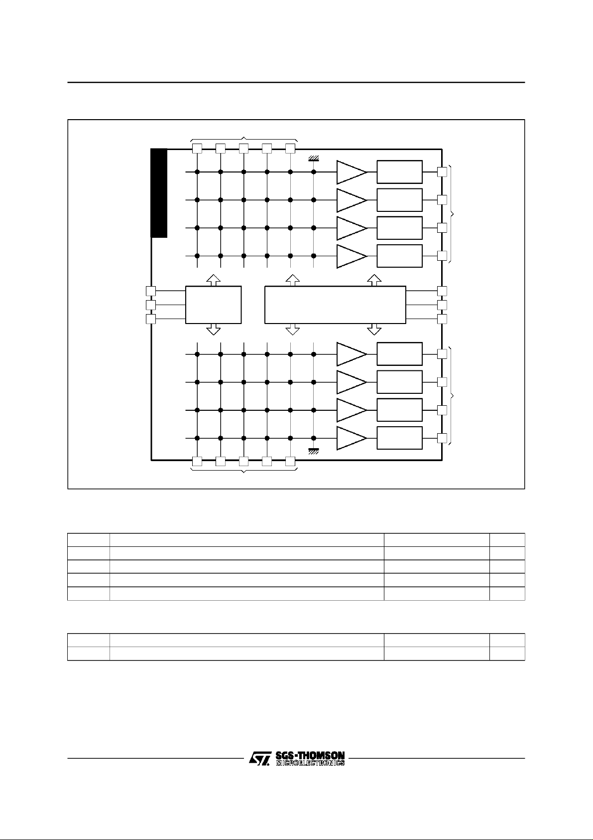
The TEA6430switches 5 stereoinputson 4 stereo
outputs, providing the customer with high quality
sound (low noise, low distortion). The 4 stereo
outputs can be set separately in high impedance
state, to enable parallel connection of several devices(up to4). All functionsare controlledthrough
2
C bus.
the I
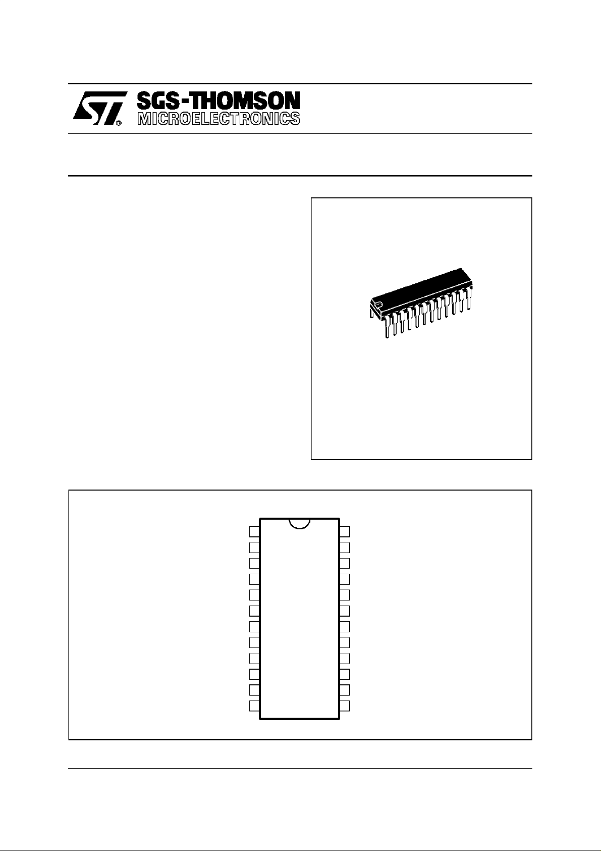
TEA6430
AUDIO CELLULAR MATRIX
SHRINK 24
(Plastic Package)
ORDER CODE : TEA6430
PINCONNECTIONS
May 1996
GND
REF
V
L1 IN
L2 IN
L3 IN
L4 IN
L5 IN
L1 OUT
R1 OUT
L2 OUT
R2 OUT
CC
1
2
3
4
5
6
7
8
9
10
11
12
24
23
22
21
20
19
18
17
16
15
14
13
SDA
SCL
SUB
R1 IN
R2 IN
R3 IN
R4 IN
R5 IN
R4 OUT
L4 OUT
R3 OUT
L3 OUT
6430-01.EPS
1/10
TEA6430
BLOCK DIAGRAM
RIGHT INPUTS
21 20 19 18 17
T
E
GAIN
A
6
4
G
3
0
G
G
3 STATES
OUT
3 STATES
OUT
3 STATES
OUT
3 STATES
OUT
10
12
14
RIGHT OUTPUTS
16
V
GND
3
S
2
C
1
SUPPLY BUS DECODER
G
G
G
3 STATES
OUT
3 STATES
OUT
3 STATES
OUT
24
SDA
23
SCL
22
ADR
15
13
11
LEFT OUTPUTS
45678
G
3 STATES
OUT
9
LEFT INPUTS
The output loads have to be larger than 2kΩ (typical 10kΩ) and 1500pF
ABSOLUTEMAXIMUM RATINGS
Symbol Parameter Value Unit
V
V
T
oper
T
Supply Voltage 12 V
CC
Voltage at Pin i to GND 0, V
I
CC
Operating Ambient Temperature 0, + 70
Storage Temperature -20, + 150
stg
6430-02.EPS
V
o
C
o
C
6430-01.TBL
THERMALDATA
Symbol Parameter Value Unit
Junction-ambient Thermal Resistance 75
2/10
R
th (j-a)
o
C/W
6430-02.TBL
TEA6430
ELECTRICALCHARACTERISTICS
=8V,T
(V
CC
3-stateis controlledby I
Symbol Parameter Test Conditions Min. Typ. Max. Unit
SUPPLY
V
CC
I
CC
RR Ripple Rejection V
AUDIO INPUTS
V
IN
V
DC
R
I
AUDIO OUTPUTS
R
OUT
Z
HI
V
OFF
V
OUT
V
N
G Gain B = 20-20kHz, R
THD Distortion V
V
CL
C
S
C
L
Notes : 1. DC offset change is less than maximum limit, in all configurations (one or several devices in parallel), provided that the
2. Flatfilter according to CCIR-468-4, B = 20Hz-20kHz
3. Measured from any selected output which contains no signal to a set of other outputs.
=25oC, RL=10kΩ,RG=600Ω, f = 1kHz, G = 0dB,VIN= 0.5V
amb
2
C bus, unlessotherwisespecified)
RMS
;
Supply Voltage 7.2 8 10.2 V
Supply Current 4 7 10 mA
IN
= 0.5V
, f = 1kHz 70 dB
RMS
Max. Signal Amplitude 2 V
Input DC Level VCC/2 V
Input Resistance 30 50 100 kΩ
Output Resistance 60 100 Ω
Output ”off” Impedance f = 20kHz, outputdisabled 50 kΩ
DC Offset Change Switching between inputs,see note 1 0.1 5 mV
Output DC Level 0.4 V
CCVCC
/2 0.6 V
CC
Output Noise Voltage B = 20-20kHz, flat, see note 2 2.5 µV
=2kΩ -0.5 0 +0.5 dB
L
Isolation ”off” State f = 1kHz, output disabled 85 dB
IN
=1V
, f = 1kHz 0.01 0.05 %
RMS
Clipping Level d = 0.3% 2 2.3 V
L, R Channel Separation f = 1kHz -85 dB
Crosstalk Audio Channels f = 1kHz, seenote 3 -85 -100 dB
Load Capacitance 1500 pF
reference Pins (P2) are all connected together.
RMS
V
RMS
6430-03.TBL
3/10

TEA6430
I2C BUS CHARACTERISTICS
Symbol Parameter
SCL
Low Level Input Voltage - 0.3 + 1.5 - 0.3 + 1.5 V
V
IL
V
High Level Input Voltage 3.0 VCC+ 0.5 3.0 VCC+ 0.5 V
IH
Input Leakage Current VI= 0 to V
I
LI
f
SDA
V
TIMING
t
t
HIGH
t
SU, DAT
t
HD,DAT
t
SU, STO
t
t
HD, STA
t
SU, STA
Clock Frequency 0 100 0 400 kHz
SCL
t
Input Rise Time 1.5V to 3V 1000 300 ns
R
Input Fall Time 1.5V to 3V 300 300 ns
t
F
C
Input Capacitance 10 10 pF
I
V
Low Level Input Voltage - 0.3 + 1.5 - 0.3 + 1.5 V
IL
V
High Level Input Voltage 3.0 VCC+ 0.5 3.0 VCC+ 0.5 V
IH
I
Input Leakage Current VI= 0 to V
LI
Input Capacitance 10 10 pF
C
I
t
Input Rise Time 1.5V to 3V 1000 300 ns
R
t
Input Fall Time 1.5V to 3V 300 300 ns
F
Low Level Output Voltage IOL= 3mA 0.4 0.4 V
OL
t
Output Fall Time 3V to 1.5V 250 250 ns
F
Load Capacitance 400 400 pF
C
L
Clock Low Period 4.7 1.3 ms
LOW
Clock High Period 4.0 0.6 ms
Data Set-upTime 250 100 ns
Data Hold Time 0 340 0 340 ns
Set-up Time fromClock High to Stop 4.0 0.6 µs
Start Set-up Time following a Stop 4.7 1.3 µs
BUF
Start Hold Time 4.0 0.6 µs
Start Set-up Time
following Clock Low-to High Transition
Test
Conditions
DD
DD
Standard Mode Fast Mode
Min. Max. Min. Max.
Unit
-10+10-10+10µA
-10+10-10+10µA
4.7 0.6 µs
6430-04.TBL
Figure1 :I2C Bus Timing
SDA
t
BUF
SCL
SDA
4/10
t
HD,STA
t
LOW
t
r
t
SU,STA t
t
HD,DAT
t
HIGH
t
f
t
SU,DAT
SU,STO
6430-03.EPS

TEA6430
I2C BUS SELECTION
2
I
C BusSlave Address
Address A6 A5 A4 A3 A2 A1 A0 R/W
Value 10011A1A00
Sub-address I2C
Symbol Parameter Conditions Pin 22 Voltage (typ.) Unit
Vsub Slaveaddress HEXA Sub-address (see note)
1
2
3
4
Note : The first3 levelsare defined by connecting the sub-address pinto the appropriate level. Sub-address4 will be selectedwhen
this pin is left open.
98
9E
9C
9A
0
1
1
0
DataByte
b7 b6 b5 b4 b3 b2 b1 b0
T0100G1G0I2I1I0
A1
*
*
Input
Select
*
*
*
*
*
Output
Select
*
*
*
*
Gain
*
*
*
Tri-state
Example : 00111100 enables L(R)2 out and connectit with a gain of 0dB to L(R)5 in.
0
1
*
*
*
*
*
*
0
0
1
1
*
*
*
*
*
*
*
*
*
*
*
*
0
1
0
1
*
*
*
*
*
*
*
*
*
*
*
*
*
*
*
*
0
0
1
1
*
*
A0
0
1
0
1
GND
V
CC
1/3
2/3
V
V
V
CC
V
CC
Action
*
*
*
*
*
*
*
*
*
*
0
1
0
1
*
*
0
0
0
0
1
1
*
*
*
*
*
*
*
*
*
*
0
0
1
1
0
0
*
*
*
*
*
*
*
*
*
*
0
1
0
1
0
1
*
*
*
*
*
*
*
*
*
*
IN1
IN2
IN3
IN4
IN5
Mute
OUT1
OUT2
OUT3
OUT4
6dB
4dB
2dB
0dB
Low impedance
Tri-state
Power On Reset
When active : outputs in 3-state. All outputs are disabled and L(R)5 is selected to drive all outputs.
Gain= 0dB.
Symbol Parameter Conditions Min. Typ. Max. Unit
Reset Start of Reset
End of Reset
Incr. V
Decr. V
Incr. V
CC
CC
CC
4.5
2.5
4.2
V
V
V
5/10

TEA6430
TYPICALPERFORMANCES
Figure 1 : Supply Current as a Function of
SupplyVoltage
10
=25°C
T
A
9
All outputs enabled
8
Figure2 : Supply Current as a Functionof
Temperature
8
V=8V
CC
All outputsenabled
7
7
6
SUPPLYCURRENT(mA)
5
78910 11 12
SUPPLY VOLTAGE(V)
Figure 3 : Ripple Rejection as a Function of
SupplyVoltage
89
Gain = 0dB
V = 600mV
T=25°C
87
A
RMSIN
85
RIPPLEREJECTION(dB)
83
7 8 9 101112
SUPPLY VOLTAGE (V)
Figure 5 : Ripple Rejection as a Function of
Gain
90
V=8V
CC
T
85
80
75
70
RIPPLEREJECTION(dB)
65
0246
GAIN (dB)
=25°C
A
V = 600mV
6
SUPPLYCURRENT(mA)
5
-20 0 20 40 60 80
6430-04.EPS
TEMPERATURE (°C)
6430-05.EPS
Figure4 : Ripple Rejection as a Functionof
Temperature
88
87
86
85
V=8V
CC
Gain = 0dB
RIPPLEREJECTION(dB)
84
f=1kHz
All outputsenabled
83
-20 0 20 40 60 80
6430-06.EPS
TEMPERATURE (°C)
6430-07.EPS
Figure6 : Clipping Level as a Function of
Supply Voltage
3.7
T=25°C
3.5
RMS
RMSIN
3.3
3.1
2.9
2.7
2.5
2.3
CLIPPING LEVEL (V )
2.1
1.9
6430-08.EPS
A
Distortion= 0.3%
Gain = 0dB
7891011 12
SUPPLY VOLTAGE(V)
6430-09.EPS
6/10

TYPICALPERFORMANCES (continued)
Figure 7 : Distortion as a Functionof
InputLevel
1
T =25°C
A
0.8
V=8V
CC
f = 1kHz
Gain = 0dB
0.6
TEA6430
Figure8 : Distortion as a Function of Gain
0.05
T
=25°C
A
V=8V
0.04
0.03
CC
f = 1kHz
V =1
OUT RMS
V
0.4
0.2
DISTORTION RATE (%)
0
0.4 0.8 2 2.4
V
INVRMS
1.61.2
(V)-
Figure 9 : CrosstalkLevel as a Functionof
Frequency(Gain= 0dB)
99
V=8V
CC
95
91
87
83
CROSSTALKLEVEL(dB)
79
048121622
FREQUENCY(kHz)
Gain= 0dB
V=2V
OUT RMS
T=25°C
A
0.02
0.01
DISTORTIONRATE(%)
6430-10.EPS
0
2 6
GAIN (dB)
4
Figure10 : CrosstalkLevel as a Function of
Frequency(Gain = 6dB)
91
89
87
85
83
81
CROSSTALKLEVEL(dB)
79
77
048121622
6430-12.EPS
FREQUENCY(kHz)
V=8V
CC
Gain= 6dB
T=25°C
A
6430-11.EPS
6430-13.EPS
7/10

TEA6430
PINCONFIGURATIONS
Figure11 : AudioIN
Pins 4 - 5 - 6 - 7 - 8
17 - 18 - 19 - 20 - 21
L (R) x in
x = 1, 2, 3, 4
Figure13 : PROG
TRI-STATE
50kΩ
Matrix
Point
VCC/2
Figure12 : Audio OUT
V
CC
TRI-STATE
V
CC
Pins 9 - 10
11 - 12- 13
14 - 15 - 16
L (R) x out
10kΩ
x = 1, 2, 3, 4
TRI-STATE
6430-14.EPS
6430-15.EPS
Figure14 : BusInputs
V
CC
V
CC
ESD
PROT.
22
40kΩ 20kΩ
3 TIMES IN //
V
REFi
to CM OS
6430-16.EPS
Pins
23 - 24
For SDA only
ACKN
X4
V
REF
to CMOS
6430-17.EPS
8/10

TYPICALAPPLICATION
VCC(+8V)
100nF
C1
C2
LEFT
INPUTS
[1, 5]
C3
C4
C5
1
2
3
4
5
6
7
8
9
10
11
12 13
22µF
T
E
A
6
4
3
0
24
23
22
21
20
19
18
17
16
15
14
SDA
SCL
C27
C25
I C
C28
C26
C24
TEA6430
2
RIGHT
INPUTS
[1, 5]
RIGHT
INPUTS
[6, 10]
*C1toC28=4.7µF
C6
C8
C10
100nF
C7
C9
C11 C13
C12 C14
RL
OUT 1
R L
OUT 2
T
E
A
6
4
3
0
24
23
22
21
20
19
18
17
16
15
14
1
2
3
4
5
6
7
8
9
10
11
12 13
V
CC
C15 C17
C16 C18
RL
OUT 3
C22
C20
RL
OUT 4
SDA
SCL
I C
C23
C21
C19
2
RIGHT
INPUTS
[6, 10]
6430-18.EPS
9/10

TEA6430
PACKAGE MECHANICALDATA
24 PINS- PLASTICSHRINK DIP
BeB1
A1
A2
Stand-off
E
E1
LA
e1
e2
SDIP24
c
E
.015
0,38
Gage Plane
e3
e2
Dimensions
D
24
1
13
F
12
Millimeters Inches
Min. Typ. Max. Min. Typ. Max.
A 5.08 0.20
A1 0.51 0.020
A2 3.05 3.30 4.57 0.120 0.130 0.180
B 0.36 0.46 0.56 0.0142 0.0181 0.0220
B1 0.76 1.02 1.14 0.030 0.040 0.045
C 0.23 0.25 0.38 0.0090 0.0098 0.0150
D 22.61 22.86 23.11 0.890 0.90 0.910
E 7.62 8.64 0.30 0.340
E1 6.10 6.40 6.86 0.240 0.252 0270
e 1.778 0.070
e1 7.62 0.30
e2 10.92 0.430
e3 1.52 0.060
L 2.54 3.30 3.81 0.10 0.130 0.150
PMSDIP24.EPS
SDIP24.TBL
Information furnished is believed tobe accurate and reliable. However,SGS-THOMSON Microelectronics assumes no responsibility
for the consequences of use of suchinformation nor forany infringement of patents or other rights of third parties which may result
from its use. No licence is granted by implication or otherwiseunder anypatent or patent rights of SGS-THOMSON Microelectronics.
Specifications mentioned in this publication are subject to change without notice. This publication supersedes and replaces all
information previously supplied. SGS-THOMSON Microelectronics products are not authorized for use as critical components in life
support devices or systems withoutexpress written approval of SGS-THOMSON Microelectronics.
1996 SGS-THOMSON Microelectronics - All Rights Reserved
Purchase of I
2
I
C Patent. Rights to use these components in a I2C system,is granted provided that the system conforms to
2
C Components of SGS-THOMSON Microelectronics,conveys a license under the Philips
2
the I
C Standard Specifications as defined by Philips.
SGS-THOMSON Microelectronics GROUP OF COMPANIES
Australia - Brazil - Canada - China - France - Germany - Hong Kong - Italy - Japan - Korea - Malaysia - Malta- Morocco
The Netherlands - Singapore -Spain - Sweden - Switzerland - Taiwan - Thailand - United Kingdom - U.S.A.
10/10
 Loading...