

SGS Thomson Microelectronics ST72T141K2M6, ST72T141K2B6 Datasheet
8-BIT MCU WITH ELECTRIC-MOTOR CONTROL,
ADC, 16-BIT TIMERS, SPI INTERFACE
■ Memories
– 8K Program memory
(ROM/OTP/EPROM)
– 256 Bytes RAM
■ Clock, Reset and Supply Management
– Enhanced reset system
– Low voltage supply supervisor
– 3 Power saving modes
■ 14 I/O Ports
– 14 multifunctional bidirectional I/O lines with:
External interruptcapability (2 vectors), 13 alternate function lines, 3 high sink outputs
■ Motor Control peripheral
– 6 PWM output channels
– Emergency pin toforce outputs to HiZ state
– 3 analog inputs for rotor position detection
with no need for additional sensors
– Comparator for current limitation
■ 3 Timers
– Two 16-bittimers with: 2 input captures, 2out-
put compares,external clock input, PWM and
Pulse generator modes
– Watchdog timer for system integrity
■ Communications Interface
– SPI synchronous serial interface
■ Analog Peripheral
– 8-bit ADC with 8 input pins
Device Summary
Features ST72141K2
Program memory - bytes 8K
RAM (stack) - bytes 256 (64)
Peripherals
Operating Supply 4V to 5.5V
CPU Frequency 4 or 8 MHz (with 8 or 16 MHz oscillator)
Operating Temperature -40°C to +85°C
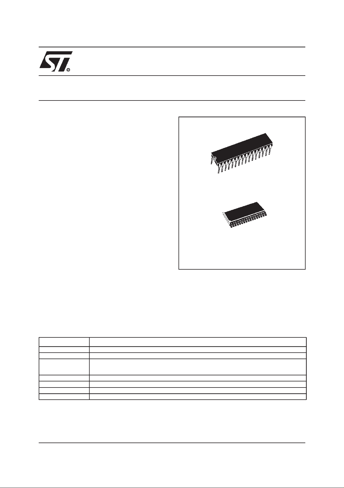
Packages SO34 / SDIP32
■ Instruction Set
– 8-bit data manipulation
– 63 basic instructions
– 17 main addressing modes
– 8 x 8 unsigned multiply instruction
– True bit manipulation
■ Development Tools
– Full hardware/softwaredevelopment package
Motor control,
Watchdog, Two 16-bit timers,
SPI, ADC
ST72141K
PRELIMINARY DATA
SDIP32
SO34S
Rev. 1.6
September 2000 1/132
This ispreliminary information on anew product in development or undergoing evaluation. Details are subject tochange without notice.
1

Table of Contents
1 GENERAL DESCRIPTION . . . . . . ................................................ 5
1.1 INTRODUCTION . . . . . .. . . . . . ............................................. 5
1.2 PIN DESCRIPTION . . ..................................................... 6
1.3 EXTERNAL CONNECTIONS . . . . . . . . . .. . . . . . . . . . . . . . . . . . . . . . . . . . . . . ......... 9
1.4 REGISTER & MEMORY MAP . . ............................................10
1.5 EPROM PROGRAM MEMORY . . . . . . . . . . . . . . . . . . .. . . . . . .................... 13
2 CENTRAL PROCESSING UNIT . . ............................................... 14
2.1 INTRODUCTION . . . . . .. . . . . . ............................................14
2.2 MAIN FEATURES . . . . . . . . . . . . . . . . . . . . . . . . . .............................. 14
2.3 CPU REGISTERS . . . .................................................... 14
3 SUPPLY, RESET AND CLOCK MANAGEMENT . . . . ................................17
3.1 LOW VOLTAGE DETECTOR (LVD) . . . . . . . . . . . . . . ........................... 18
3.2 RESET MANAGER . . .................................................... 19
3.3 LOW CONSUMPTION OSCILLATOR . . . . . . . .. . . . . . . . . . . . . . . . . . . . . ........... 23
3.4 MAIN CLOCK CONTROLLER (MCC) . . . . ....................................24
4 INTERRUPTS . . .............................................................25
4.1 NON MASKABLE SOFTWARE INTERRUPT .................................. 25
4.2 EXTERNAL INTERRUPTS . . . . . . . . . . . . . . . . . . .............................. 25
4.3 PERIPHERAL INTERRUPTS ............................................... 25
5 POWER SAVING MODES . . . . . . . . . . ...........................................28
5.1 INTRODUCTION . . . . . .. . . . . . ............................................28
5.2 HALT MODE . . . . . . . . . . . . . . . . . . . ........................................ 29
5.3 WAIT MODE . . . . .. . . . . . . . . . . . . . . . . . . . . . . . . . . . .. . . . . . . . . .. . . . . . . ........ 30
5.4 SLOW MODE . . . . . . . . . . . . . . . . . . . . . . . . . . ................................. 30
6 I/O PORTS . . . . . . . . . . . . . . . . . . . . . . . . . . ........................................31
6.1 INTRODUCTION . . . . . .. . . . . . ............................................31
6.2 FUNCTIONAL DESCRIPTION . . . . . ......................................... 31
6.2.1 Input Modes . . . . . . . . . . . . . . . . . . . . . . ................................. 31
6.2.2 Output Modes . . . . . . ...............................................31
6.2.3 Alternate Functions . . ...............................................31
6.3 I/O PORT IMPLEMENTATION . . . . . . . . . . . . . . . . . . . . . . . . . . . . . . . . . . . . . . . . . . . . . . 34
6.3.1 Register Description . . . . . ............................................36
7 MISCELLANEOUS REGISTER . . ...............................................38
7.1 I/O PORT INTERRUPT SENSITIVITY DESCRIPTION . . . . . .. . . . . . . . . . . . . . . . . . . . . 38
7.2 I/O PORT ALTERNATE FUNCTIONS . . . . . . . . ................................ 38
7.3 CLOCK PRESCALERSELECTION . . ........................................ 38
7.4 MISCELLANEOUS REGISTER DESCRIPTION . . . . . . . . . . . . . . . . . . . . . . . . . . . . . . . . 39
8 ON-CHIP PERIPHERALS . . . . . . . . . . . ........................................... 40
8.1 MOTOR CONTROLLER (MTC) . . . . ......................................... 40
8.1.1 Introduction . . . .................................................... 40
8.1.2 Main Features . . . . . . ...............................................40
8.1.3 Application Example . . . . . . . . . . . . . . . . . . .............................. 40
8.1.4 Functional Description . . . . ...........................................44
132
2/132
2

Table of Contents
8.1.5 Low PowerModes . . . ...............................................66
8.1.6 Interrupts . . . . . . . . . . . . . . . . . . . . . . . . ................................. 66
8.1.7 Register Description . . . . . ............................................67
8.2 WATCHDOG TIMER (WDG) . .. . . . . . . . . . . . . . . . . . . . . . . . . . . . . . . . . . . . . . . . . . . . . 75
8.2.1 Introduction . . . .................................................... 75
8.2.2 Main Features . . . . . . ...............................................75
8.2.3 Functional Description . . . . ...........................................76
8.2.4 Low PowerModes . . . ...............................................76
8.2.5 Interrupts . . . . . . . . . . . . . . . . . . . . . . . . ................................. 76
8.2.6 Register Description . . . . . ............................................76
8.3 16-BIT TIMER . . . . . . . . . . . . . . . . . . ........................................78
8.3.1 Introduction . . . .................................................... 78
8.3.2 Main Features . . . . . . ...............................................78
8.3.3 Functional Description . . . . ...........................................78
8.3.4 Low PowerModes . . ............................................... 90
8.3.5 Interrupts . . . . . ....................................................90
8.3.6 Summary of Timer modes . . . . . . . . . . . . . . .............................. 90
8.3.7 Register Description . . . . . ............................................91
8.4 SERIAL PERIPHERAL INTERFACE (SPI) . . . .. . . . . . . . . . . . . .. . . . . . ............96
8.4.1 Introduction . . . .................................................... 96
8.4.2 Main Features . . . . . . ...............................................96
8.4.3 General description . . . . . . . . . . . . . . . . . . . . . . . . . . . . . . . . . . . . . . . . . . . . . . . . . 96
8.4.4 Functional Description . . . . ...........................................98
8.4.5 Low PowerModes . . . ..............................................105
8.4.6 Interrupts . . . . . ...................................................105
8.4.7 Register Description . . . . . ...........................................106
8.5 8-BIT A/D CONVERTER (ADC) . . . . . . . .. . . . . . .. . . .......................... 109
8.5.1 Introduction . . . ................................................... 109
8.5.2 Main Features . . . . . . .............................................. 109
8.5.3 Functional Description . . . . ..........................................110
8.5.4 Low PowerModes . . . ..............................................110
8.5.5 Interrupts . . . . . . . . . . . . . . . . . . . . . . . . ................................ 110
8.5.6 Register Description . . . . . ...........................................111
9 INSTRUCTION SET . . . . . . . . . . . . . . . . . . .......................................112
9.1 ST7 ADDRESSING MODES . . . . . . . . . .. . . . . . .. . . . . . . . . . . . . . . . . . . . . . . . . . . . . 112
9.1.1 Inherent . . . . . . .. . . . .............................................. 113
9.1.2 Immediate . . . . . . . . . . . . . . . . . . . . . . . . . . . . . . . . . . . . . . . . . . . . . . . . .. . . . . . 113
9.1.3 Direct . .......................................................... 113
9.1.4 Indexed (No Offset, Short, Long) . . . . . . . . . . . . .......................... 113
9.1.5 Indirect (Short, Long) . . . . . . . . . . . . . . . .. . . . . . . . . . . . . . . . . . . . . . . . . . . . . . . 113
9.1.6 Indirect Indexed (Short, Long) . .......................................114
9.1.7 Relative Mode (Direct, Indirect) . . . . . . . . . . . . . . . . . . . . . . . . . . . . . . . . . . . . . . . 114
9.2 INSTRUCTION GROUPS . . .. . . . . . . . . . . . . ................................115
10 ELECTRICAL CHARACTERISTICS . . . . ........................................ 118
10.1ABSOLUTE MAXIMUM RATINGS . . . .......................................118
10.2RECOMMENDED OPERATING CONDITIONS . . . . . . . . . . . . . . . . . . . . . ..........119
10.3DC ELECTRICAL CHARACTERISTICS . . . . . . . . . . . . . . . . . . . .. . . . . . ........... 119
3/132
3

Table of Contents
10.4GENERAL TIMING CHARACTERISTICS . . . . . . . . . . . .. . . . . . . . . . . . . . . . . ....... 119
10.5I/O PORT CHARACTERISTICS . ........................................... 120
10.6SUPPLY, RESET AND CLOCK CHARACTERISTICS . . . . . . . . . . . . . . .. . . . . . . . . . . 121
10.6.1Supply Manager ...................................................121
10.6.2RESET Sequence Manager . . . . . . . . . . ................................121
10.6.3Clock System . . . . . . . . . . . .......................................... 121
10.7MEMORY AND PERIPHERAL CHARACTERISTICS . . . . . . . . . . . . . . . . . . . . . . . . . . . 122
11 GENERAL INFORMATION ................................................... 128
11.1PACKAGE MECHANICAL DATA . . . . . . . . . . . . . . . . . .......................... 128
11.2ORDERING INFORMATION . . . . . . . . . . . . . ................................. 129
12 SUMMARY OF CHANGES . .................................................. 131
4/132
132
1
1 GENERAL DESCRIPTION
1.1 INTRODUCTION
ST72141K
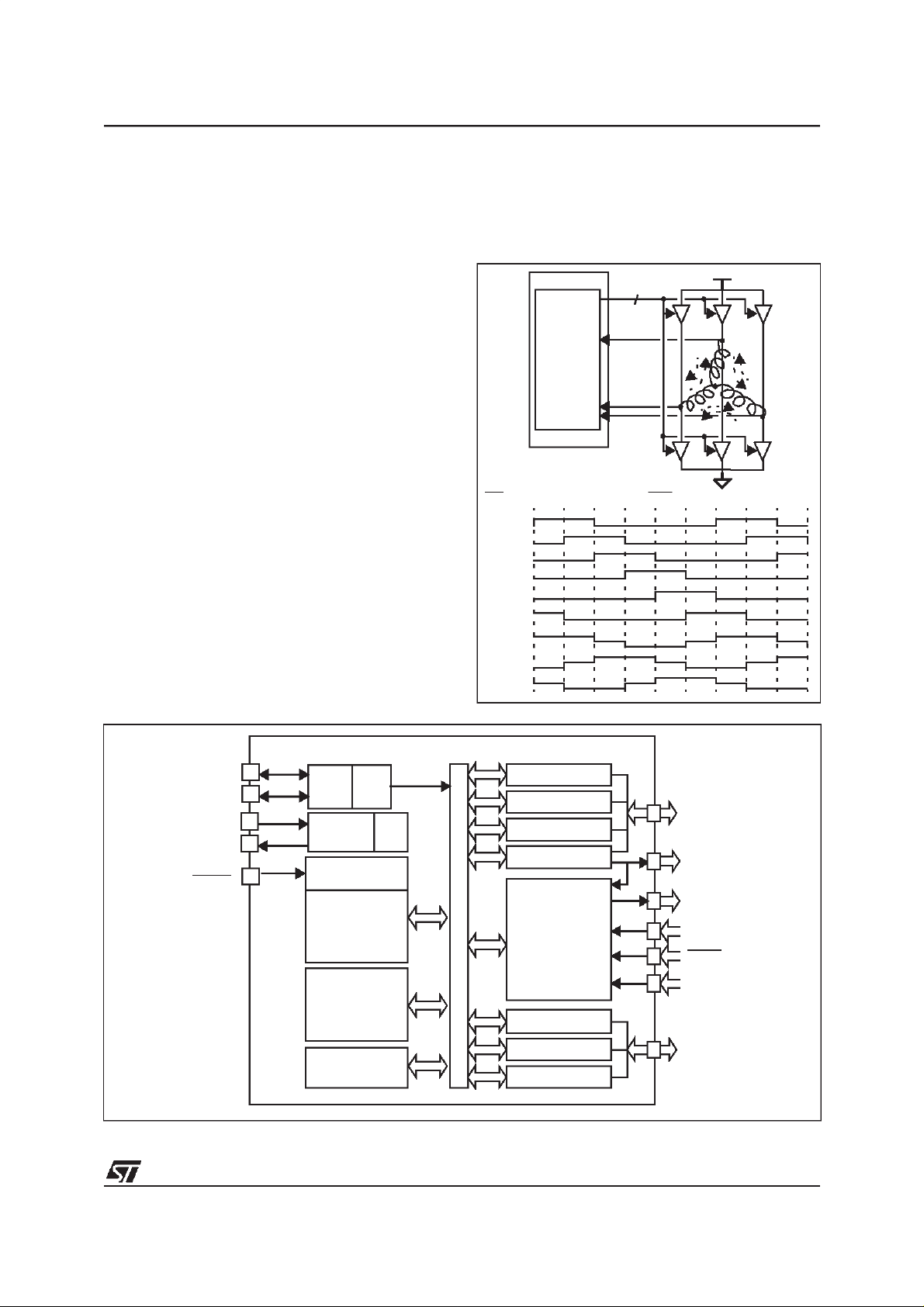
The ST72141K devices are members of the ST7
microcontroller family designed specifically for motor control applications and including A/D conversion and SPI interface capabilities. They include
an on-chip Moter Controller peripheral for control
of electric brushless moters with or without sensors. An example application, for 6-step control of
a Permanent Magnet DC motor, is shown in Figure
1.
The ST72141K devices are based on a common
industry-standard 8-bit core, featuring an enhanced instruction set.
Under software control, they can be placed in
WAIT, SLOW, or HALT mode, reducing power
consumption when the application is in idle or
standby state.
The enhanced instruction set and addressing
modes of the ST7 offer bothpower andflexibility to
software developers,enabling the design of highly
efficient and compact application code. In addition
to standard 8-bitdata management, all ST7microcontrollers feature true bit manipulation, 8x8 unsigned multiplication and indirect addressing
modes.
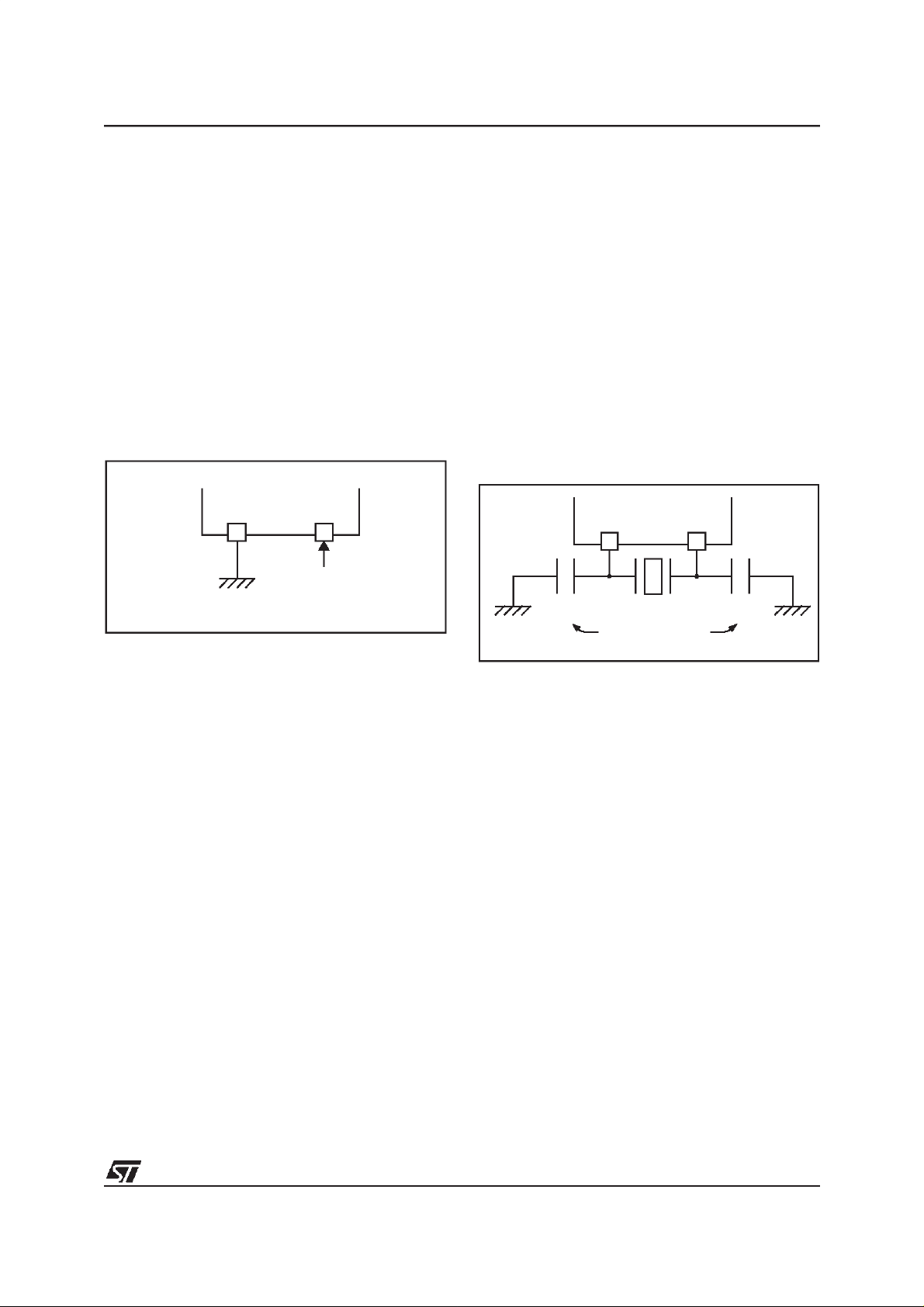
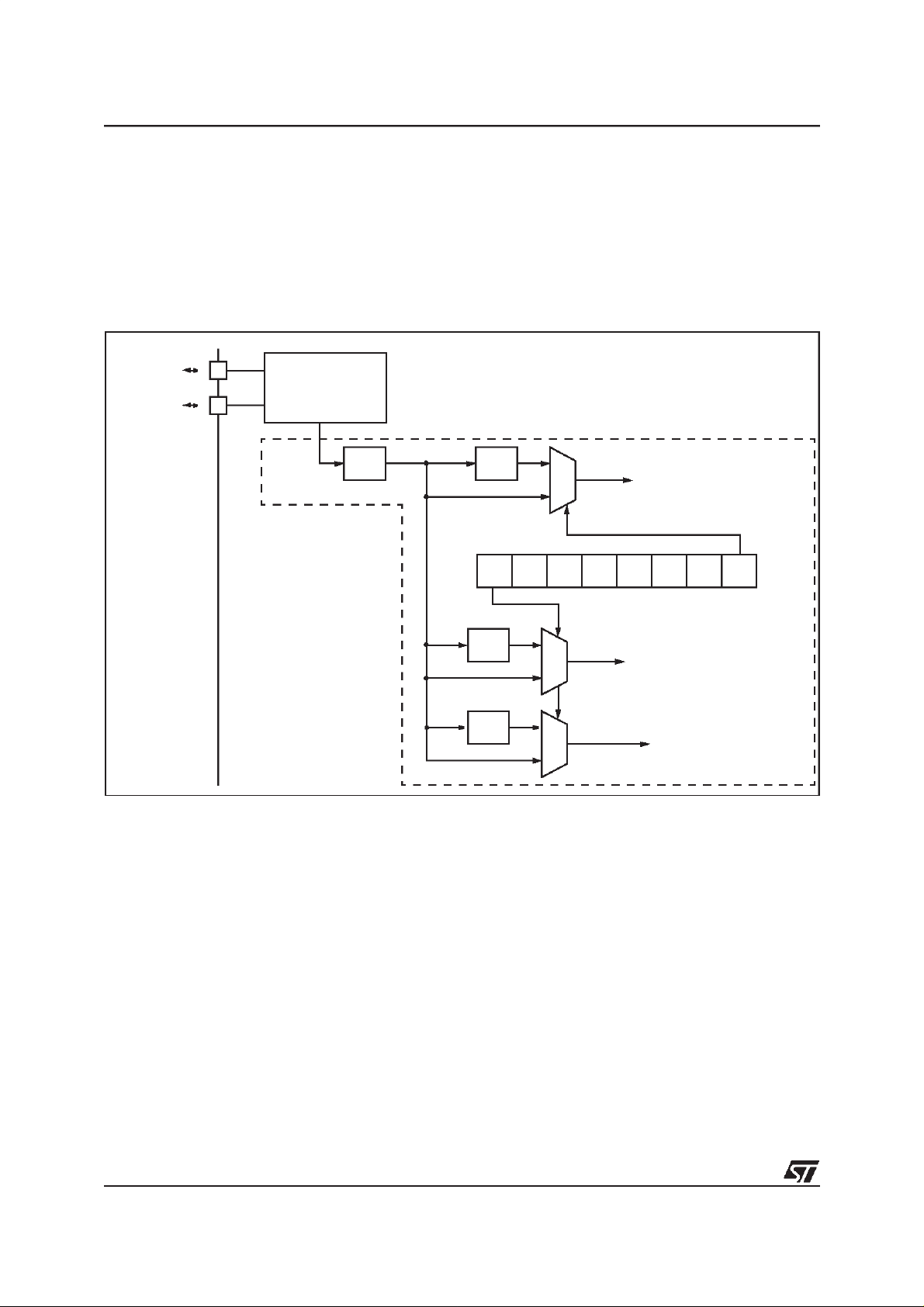
Figure 2. Device Block Diagram
Figure 1. Example of a 6-step-controlled Motor
ST7
MCO5 -0
6
MCIB
MTC
MCIA
MCIC
Net Step
Σ1Σ2Σ3Σ4Σ5Σ6Σ1Σ2Σ
0
1
2
3
4
5
300V
150V
A
0
300V
150V
B
0
300V
150V
0
C
0
I
4
A
I
35
300V
2
4
B
I
6
I
1
I
3
C
I
5
2
1
3
OSC1
OSC2
V
DD
V
SS
RESET
OSC
POWER
SUPPLY
CONTROL
8-BIT CORE
ALU
8K-EPROM
256b-RAM
DIV
LVD
Internal
CLOCK
ADDRESS AND DATA BUS
PORT A
8-BIT ADC
TIMER B
TIMER A
MOTOR CTRL
PORT B
SPI
WATCHDOG
PA7:0
(8-BIT)
OC1A
MCO5:0
MCIA:C
MCES
MCCFI
PB5:0
(6-BIT)
5/132
4
ST72141K
1.2 PIN DESCRIPTION
Figure 3. 34-Pin SO Package Pinout
MISO/PB5
MOSI/PB4
SCK/PB3
SS/ (HS) PB2
EXTCLK_B/ (HS) PB1
EXTCLK_A/ (HS) PB0
MCO5
MCO4
MCO3
MCO2
MCO1
MCO0
MCES
NC
OSC1
OSC2
RESET
1
2
3
4
5
6
7
8
9
10
11
12
13
14
15
16
17
EI1
EI0
MCIA
34
MCIB
33
MCIC
32
MCCFI
31
V
30
DD
V
29
SS
V
28
PP
OCMP1_A
27
NC
26
PA7/AIN7/OCMP2_A
25
PA6/AIN6/ICAP1_A
24
23
PA5/AIN5/ICAP2_A
PA4/AIN4/OCMP1_B
22
PA3/AIN3/OCMP2_B
21
PA2/AIN2/ICAP1_B
20
PA1/AIN1/ICAP2_B
19
PA0/AIN0
18
Figure 4. 32-Pin SDIP Package Pinout
MCO5
MCO4
MCO3
MCO2
MCO1
MCO0
MCES
MISO/PB5
MOSI/PB4
SCK/PB3
SS/ (HS) PB2
EXTCLK_B/ (HS) PB1
EXTCLK_A/ (HS) PB0
OSC1
OSC2
RESET
1
2
3
4
5
6
7
8
9
10
11
12
13
14
15
16
EI0
EI1
MCIA
32
MCIB
31
MCIC
30
MCCFI
29
V
28
27
26
25
24
23
22
21
20
19
18
17
DD
V
SS
V
PP
OCMP1_A
PA7/AIN7/OCMP2_A
PA6/AIN6/ICAP1_A
PA5/AIN5/ICAP2_A
PA4/AIN4/OCMP1_B
PA3/AIN3/OCMP2_B
PA2/AIN2/ICAP1_B
PA1/AIN1/ICAP2_B
PA0/AIN0
6/132
5
PIN DESCRIPTION (Cont’d)
Legend / Abbreviations:
Type: I = input, O = output, S = supply
Input level: A = Dedicated analog input
In/Output level: C = CMOS 0.3VDD/0.7VDD,
CT= CMOS 0.3VDD/0.7VDDwith input trigger
Output level: HS = high sink (on N-buffer only),
R=70Ω/100Ω ratio of logical levels.
Analog level if used as PWM filtered with an external capacitor
Port configuration capabilities:
– Input: float = floating, wpu = weak pull-up, int = interrupt, ana = analog
– Output: OD = open drain, T = true open drain, PP = push-pull
Note: the Reset configuration of each pin is shown in bold.
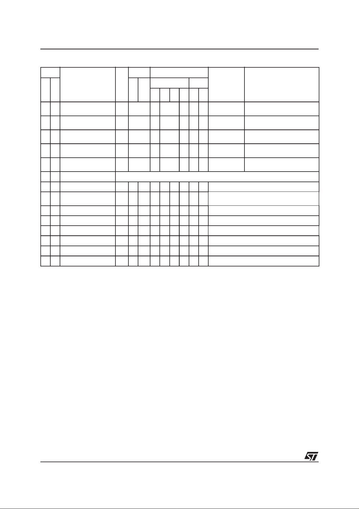
Table 1. Device Pin Description
ST72141K
Pin n°
Pin Name
SO34
SDIP32
1 1 MCO5 O C X Motor Control Output Channel 5
2 2 MCO4 O C X Motor Control Output Channel 4
3 3 MCO3 O C X Motor Control Output Channel 3
4 4 MCO2 O C X Motor Control Output Channel 2
5 5 MCO1 O C X Motor Control Output Channel 1
6 6 MCO0 O C X Motor Control Output Channel 0
7 7 MCES I C
8 8 PB5/MISO I/O C
9 NC Not Connected
9 10 PB4/MOSI I/O C
10 11 PB3/SCK I/O C
11 12 PB2/SS I/O C
12 13 PB1/EXTCLK_B I/O C
13 14 PB0/EXTCLK_A I/O C
14 15 OSC1
15 16 OSC2
16 17 RESET I/O C X X Toppriority nonmaskable interrupt (active low)
17 18 PA0/AIN0 I/O C
18 19 PA1/ICAP2_B/AIN1 I/O C
19 20 PA2/ICAP1_B/AIN2 I/O C
Level Port / Control
Input Output
Type
Input
Output
float
T
X EI1 X X Port B5 SPI Master In / Slave Out Data
T
X EI1 X X Port B4 SPI Master Out / Slave In Data
T
X EI1 X X Port B3 SPI Serial Clock
T
HS X EI1 T Port B2 SPI Slave Select (active low)
T
HS X EI1 T Port B1 Timer B Input Clock
T
HS X EI1 T Port B0 Timer A Input Clock
T
X EI0 X X X Port A0 ADC Analog Input 0
T
X EI0 X X X Port A1
T
X EI0 X X X Port A2
T
int
wpu
X Motor Control Emergency Stop Input
ana
OD
Main
Function
(after reset)
PP
These pins connect a crystal or ceramic
resonator, or an external RC, or an external
source to the on-chip oscillator
Alternate Function
Timer B Input Capture 2 or
ADC Analog Input 1
Timer B Input Capture 1 or
ADC Analog Input 2
7/132
6
ST72141K
Pin n°
Level Port / Control
Main
Pin Name
Type
SO34
SDIP32
Input
20 21 PA3/OCMP2_B/AIN3 I/O C
21 22 PA4/OCMP1_B/AIN4 I/O C
22 23 PA5/ICAP2_A/AIN5 I/O C
23 24 PA6/ICAP1_A/AIN6 I/O C
24 25 PA7/OCMP2_A/AIN7 I/O C
T
T
T
T
T
Input Output
Output
float
wpu
int
ana
OD
PP
X EI0 X X X Port A3
X EI0 X X X Port A4
X EI0 X X X Port A5
X EI0 X X X Port A6
X EI0 X X X Port A7
Function
(after reset)
Alternate Function
Timer B Output Compare 2 or
ADC Analog Input 3
Timer B Output Compare 1 or
ADC Analog Input 4
Timer A Input Capture 2 or
ADC Analog Input 5
Timer A Input Capture 1 or
ADC Analog Input 6
Timer A Output Compare 2 or
ADC Analog Input 7
26 NC Not Connected
25 27 OCMP1_A O R Timer A Output Compare 1
26 28 V
27 29 V
28 30 V
PP
SS
DD
I
S Ground
S Main power supply
Must be tied low during normal operating
mode,EPROM Programming voltage pin.
29 31 MCCFI I A Motor Control Current Feedback Input
30 32 MCIC I A Motor Control Input C
31 33 MCIB I A Motor Control Input B
32 34 MCIA I A Motor Control Input A
8/132
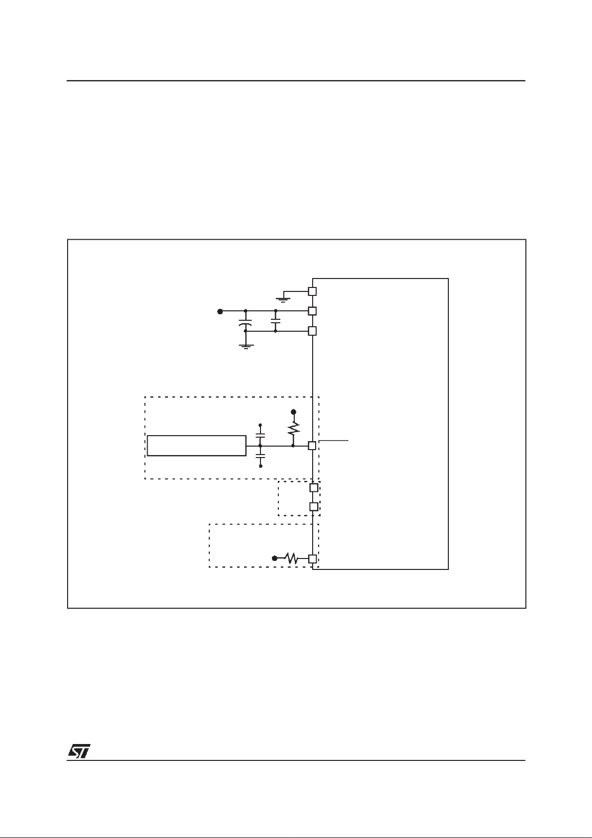
1.3 EXTERNAL CONNECTIONS
ST72141K
The following figure shows the recommended external connections for the device.
The VPPpin is only used for programming OTP
and EPROM devices and must be tied to ground in
user mode.
The 10 nF and 0.1 µF decoupling capacitors on
the power supply lines are a suggested EMC performance/cost tradeoff.
Figure 5. Recommended External Connections
V
DD
Optional if Low Voltage
Detector (LVD) isused
EXTERNAL RESET CIRCUIT
10µF
+
V
DD
0.1µF
0.1µF
V
SS
The external reset network is intended to protect
the device against parasitic resets, especially in
noisy environments.
Unused I/Os should be tied high to avoid any unnecessary power consumption on floating lines.
An alternative solution is to program the unused
ports as inputs with pull-up.
V
PP
V
V
4.7K
DD
DD
V
SS
RESET
OSC1
OSC2
0.1µF
See
Clocks
Section
Or configure unused I/O ports
by software as input with pull-up
V
10K
DD
Unused I/O
9/132
ST72141K
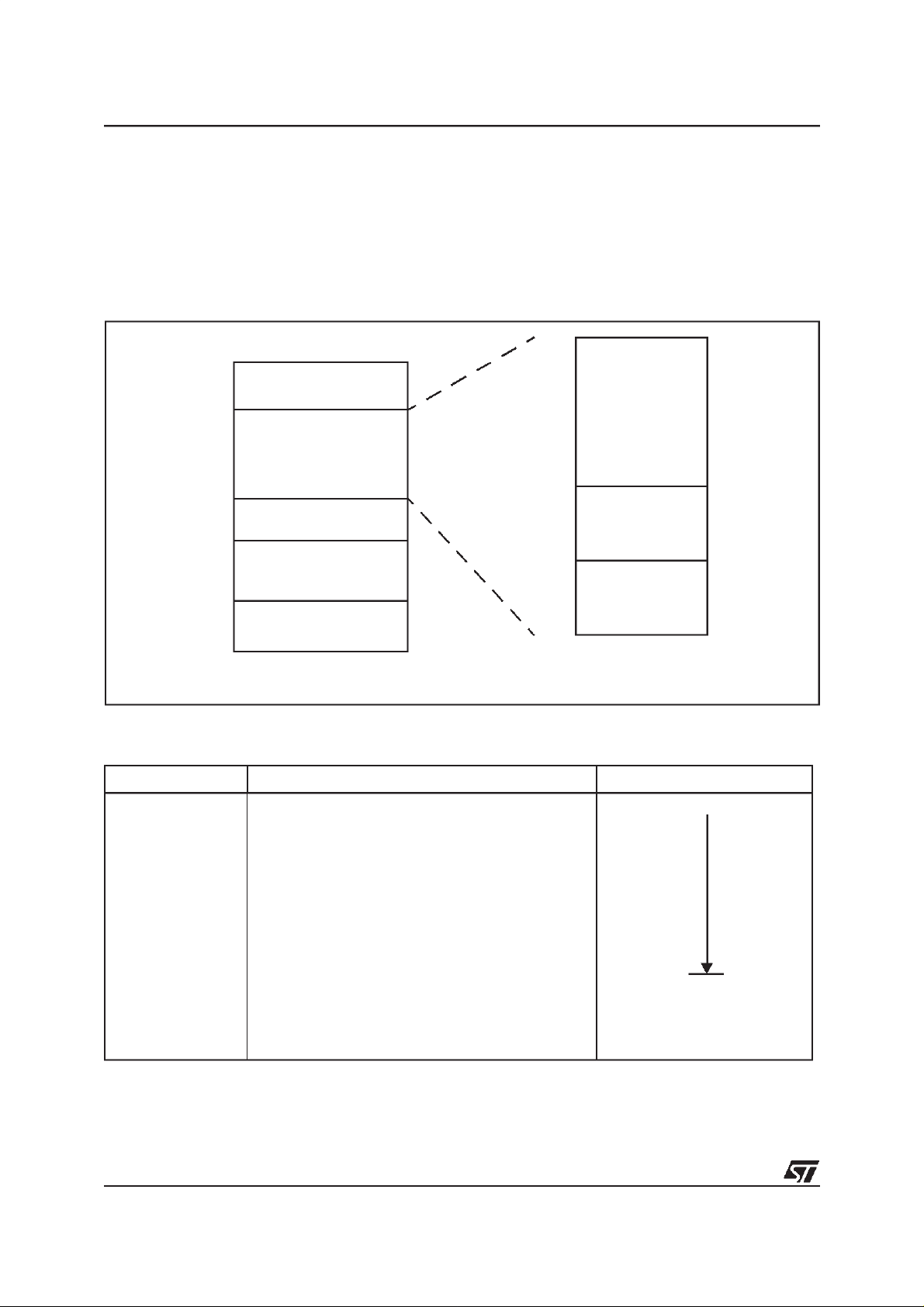
1.4 REGISTER & MEMORY MAP
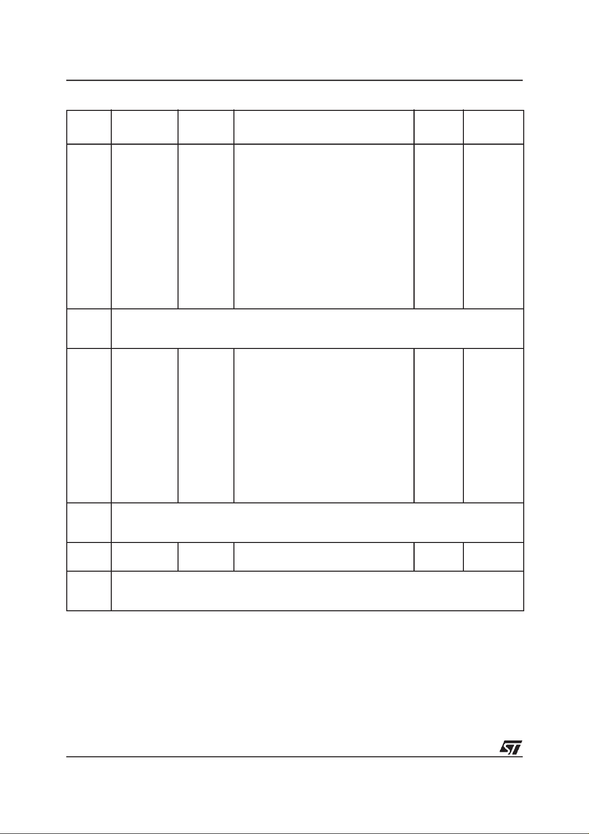
As shown in Figure 6, the MCU is capable of addressing 64K bytes of memories and I/O registers.
The available memory locations consist of 128
bytes of register locations, 256 bytes of RAM and
8Kbytes of user program memory. The RAM
Figure 6. Memory Map
0000h
007Fh
0080h
017Fh
0180h
DFFFh
E000h
FFDFh
FFE0h
FFFFh
HW Registers
(see Table 3)
256 Bytes RAM
Reserved
Program Memory
(8K Bytes)
Interrupt & Reset Vectors
(see Table 2)
space includes up to 64 bytes for the stack from
0140h to 017Fh.
The highest address bytes contain the user reset
and interrupt vectors.
0080h
Short Addressing
RAM
“Zero page”
(128 Bytes)
00FFh
0100h
013Fh
0140h
017Fh
16-bit Addressing
RAM
(64 Bytes)
Stack or
16-bit Addressing
RAM
(64 Bytes)
Table 2. Interrupt Vector Map
Vector Address Description Remarks
FFE0-FFE1h
FFE2-FFE3h
FFE4-FFE5h
FFE6-FFE7h
FFE8-FFE9h
FFEA-FFEBh
FFEC-FFEDh
FFEE-FFEFh
FFF0-FFF1h
FFF2-FFF3h
FFF4-FFF5h
FFF6-FFF7h
FFF8-FFF9h
FFFA-FFFBh
FFFC-FFFDh
FFFE-FFFFh
10/132
Not used
Not used
Not used
Not used
Not used
TIMER B interrupt vector
TIMER A interrupt vector
SPI interrupt vector
Motor control interrupt vector (events: E, O)
Motor control interrupt vector (events: C, D)
Motor control interrupt vector (events: R, Z)
External interrupt vector EI1: port B7..0
External interrupt vector EI0: port A7..0
Not used
TRAP (software) interrupt vector
RESET vector
Internal Interrupt
External Interrupt
External Interrupt
CPU Interrupt
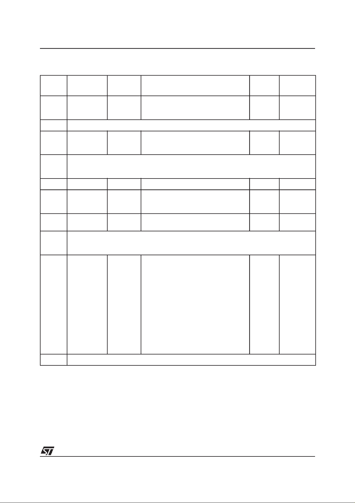
Table 3. Hardware Register Map
ST72141K
Address Block
0000h
0001h
0002h
0003h Reserved Area (1 Byte)
0004h
0005h
0006h
0007h
to
001F
0020h MISCR Miscellaneous Register 00h R/W
0021h
0022h
0023h
0024h
0025h
0026h
to
0030h
Port A
Port B
SPI
WATCHDOG
Register
Label
PADR
PADDR
PAOR
PBDR
PBDDR
PBOR
SPIDR
SPICR
SPISR
WDGCR
WDGSR
Register Name
Port A Data Register
Port A Data Direction Register
Port A Option Register
Port B Data Register
Port B Data Direction Register
Port B Option Register
Reserved Area (24 Byte)
SPI Data I/O Register
SPI Control Register
SPI Status Register
Watchdog Control Register
Watchdog Status Register
Reserved Area (11 Bytes)
Reset
Status
00h
00h
00h
00h
00h
00h
xxh
0xh
00h
7Fh
x0h
Remarks
R/W
R/W
R/W
R/W
R/W
R/W.
R/W
R/W
Read Only
R/W
Read Only
0031h
0032h
0033h
0034h
0035h
0036h
0037h
0038h
0039h
003Ah
003Bh
003Ch
003Dh
003Eh
003Fh
0040h Reserved Area (1 Byte)
TIMER A
TACR2
TACR1
TASR
TAIC1HR
TAIC1LR
TAOC1HR
TAOC1LR
TACHR
TACLR
TAACHR
TAACLR
TAIC2HR
TAIC2LR
TAOC2HR
TAOC2LR
Timer A Control Register 2
Timer A Control Register 1
Timer A Status Register
Timer A Input Capture 1 High Register
Timer A Input Capture 1 Low Register
Timer A Output Compare 1 High Register
Timer A Output Compare 1 Low Register
Timer A Counter High Register
Timer A Counter Low Register
Timer A Alternate Counter High Register
Timer A Alternate Counter Low Register
Timer A Input Capture 2 High Register
Timer A Input Capture 2 Low Register
Timer A Output Compare 2 High Register
Timer A Output Compare 2 Low Register
00h
00h
xxh
xxh
xxh
80h
00h
FFh
FCh
FFh
FCh
xxh
xxh
80h
00h
R/W
R/W
Read Only
Read Only
Read Only
R/W
R/W
Read Only
Read Only
Read Only
Read Only
Read Only
Read Only
R/W
R/W
11/132
ST72141K
Address Block
0041h
0042h
0043h
0044h
0045h
0046h
0047h
0048h
0049h
004Ah
004Bh
004Ch
004Dh
004Eh
004Fh
0050h
to
005Fh
0060h
0061h
0062h
0063h
0064h
0065h
0066h
0067h
0068h
0069h
006Ah
006Bh
006Ch
006Dh
TIMER B
MOTOR
CONTROL
Register
Label
TBCR2
TBCR1
TBSR
TBIC1HR
TBIC1LR
TBOC1HR
TBOC1LR
TBCHR
TBCLR
TBACHR
TBACLR
TBIC2HR
TBIC2LR
TBOC2HR
TBOC2LR
MTIM
MZPRV
MZREG
MCOMP
MDREG
MWGHT
MPRSR
MIMR
MISR
MCRA
MCRB
MPHST
MPAR
MPOL
Register Name
Timer B Control Register 2
Timer B Control Register 1
Timer B Status Register
Timer B Input Capture 1 High Register
Timer B Input Capture 1 Low Register
Timer B Output Compare 1 High Register
Timer B Output Compare 1 Low Register
Timer B Counter High Register
Timer B Counter Low Register
Timer B Alternate Counter High Register
Timer B Alternate Counter Low Register
Timer B Input Capture 2 High Register
Timer B Input Capture 2 Low Register
Timer B Output Compare 2 High Register
Timer B Output Compare 2 Low Register
Reserved Area (16 Bytes)
Timer Counter Register
Zn-1 Capture Register
Zn Capture Register
Compare Register
C
n+1
D capture/Compare Register
Weight Register
Prescaler and Ratio Register
Interrupt Mask Register
Interrupt Status Register
Control Register A
Control Register B
Phase State Register
Output Parity Register
Output Polarity Register
Reset
Status
00h
00h
xxh
xxh
xxh
80h
00h
FFh
FCh
FFh
FCh
xxh
xxh
80h
00h
00h
00h
00h
00h
00h
00h
00h
00h
00h
00h
00h
00h
00h
00h
Remarks
R/W
R/W
Read Only
Read Only
Read Only
R/W
R/W
Read Only
Read Only
Read Only
Read Only
Read Only
Read Only
R/W
R/W
R/W
R/W
R/W
R/W
R/W
R/W
R/W
R/W
R/W
R/W
R/W
R/W
R/W
R/W
006Eh
006Fh
0070h
0071h
0072h
007Fh
12/132
to
ADC
to
ADCDR
ADCCSR
Data Register
Control/Status Register
Reserved Area (2 bytes)
Reserved Area (14 Bytes)
00h
00h
Read Only
R/W

1.5 EPROM PROGRAM MEMORY
ST72141K
The programmemory of the OTP and EPROMdevices can be programmed with EPROM programming tools available from STMicroelectronics.
EPROM Erasure
EPROM devices are erased by exposure to high
intensity UVlightadmitted through the transparent
window. This exposure discharges the floating
gate to its initial state through induced photo current.
It is recommended that the EPROM devices be
kept out of direct sunlight, since the UV content of
sunlight can be sufficient to cause functional failure. Extended exposure to room level fluorescent
lighting may also cause erasure.
An opaque coating (paint, tape, label, etc...)
should be placed over the package window if the
product is to be operated under theselighting conditions. Covering the window also reduces IDDin
power-saving modes due to photo-diode leakage
currents.
13/132
ST72141K
2 CENTRAL PROCESSING UNIT
2.1 INTRODUCTION
This CPU has a full 8-bit architecture and contains
six internal registers allowing efficient 8-bit data
manipulation.
2.2 MAIN FEATURES
■ 63 basic instructions
■ Fast 8-bit by 8-bit multiply
■ 17 main addressing modes
■ Two 8-bit index registers
■ 16-bit stack pointer
■ Low power modes
■ Maskable hardware interrupts
■ Non-maskable software interrupt
2.3 CPU REGISTERS
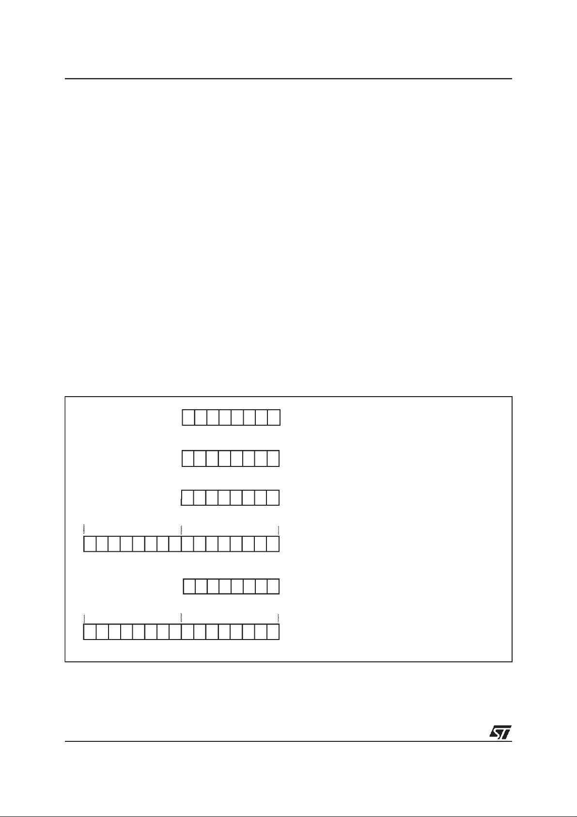
The 6 CPU registers shown in Figure 7 are not
present in the memory mapping and are accessed
by specific instructions.
Figure 7. CPU Registers
70
RESET VALUE = XXh
70
RESET VALUE = XXh
70
RESET VALUE= XXh
Accumulator (A)
The Accumulator is an 8-bit general purpose register used to hold operands and the results of the
arithmetic and logic calculations and to manipulate
data.
Index Registers (X and Y)
In indexed addressing modes, these 8-bitregisters
are used to create either effective addresses or
temporary storage areas for data manipulation.
(The Cross-Assembler generates a precede instruction (PRE) to indicate that the following instruction refers to the Y register.)
The Y registeris not affectedby the interrupt automatic procedures (notpushed to and popped from
the stack).
Program Counter (PC)
The program counter is a 16-bit register containing
the address of the next instruction to be executed
by the CPU. It is made of two 8-bit registers PCL
(Program Counter Low which is the LSB) andPCH
(Program CounterHigh which is the MSB).
ACCUMULATOR
X INDEX REGISTER
Y INDEX REGISTER
15 8
RESET VALUE = RESET VECTOR @ FFFEh-FFFFh
15
RESET VALUE = STACKHIGHER ADDRESS
14/132
PCH
RESET VALUE =
7
70
1C11HINZ
1X11X1XX
87 0
PCL
0
PROGRAM COUNTER
CONDITION CODE REGISTER
STACK POINTER
X = Undefined Value

CPU REGISTERS (Cont’d)
CONDITION CODE REGISTER (CC)
Read/Write
Reset Value: 111x1xxx
70
111HINZC
The 8-bit Condition Code register contains the interrupt mask and four flags representative of the
result ofthe instruction just executed. This register
can also be handled by the PUSH and POP instructions.
These bits can be individually tested and/or controlled by specific instructions.
because the I bit is set by hardware at the start of
the routine and reset by the IRET instruction at the
end of theroutine. If the I bit is cleared bysoftware
in the interrupt routine, pending interrupts are
serviced regardless of the priority level of the current interrupt routine.
Bit 2 = N
Negative
.
This bit is set and cleared by hardware. It is representative of the result sign of the last arithmetic,
logical or data manipulation. It is a copy of the 7
bit of the result.
0:Theresultof the last operation is positive or null.
1: The result of the last operation is negative
(i.e. the most significant bit is a logic 1).
This bit isaccessed bythe JRMI andJRPL instruc-
Bit 4 = H
Half carry
.
tions.
This bit is set by hardware whena carryoccursbetween bits 3 and 4 of the ALU during an ADD or
ADC instruction. It is resetby hardware during the
same instructions.
0: No half carry has occurred.
1: A half carry has occurred.
This bit is tested using the JRH or JRNH instruction. The H bit is useful in BCD arithmetic subroutines.
Bit 1 = Z
Zero
.
This bit is set and cleared by hardware. Thisbit indicates that the result of the last arithmetic, logical
or data manipulation is zero.
0: The result of the last operation is different from
zero.
1: The result of the last operation is zero.
This bit is accessed by the JREQ and JRNE test
instructions.
Bit 3 = I
This bit is set by hardware when entering in inter-
rupt or by software to disable all interrupts except
the TRAP software interrupt. This bit is cleared by
software.
0: Interrupts are enabled.
1: Interrupts are disabled.
This bit is controlledby the RIM, SIM and IRET instructions and is tested by the JRM and JRNM instructions.
Note: Interrupts requested while I is set are
latched and can be processed when I is cleared.
Interrupt mask
.
Bit 0 = C
Carry/borrow.
This bit is set and cleared by hardware and software. It indicates an overflow or an underflow has
occurred during the last arithmetic operation.
0: No overflow or underflow has occurred.
1: An overflow or underflow hasoccurred.
This bit is driven by the SCF and RCF instructions
and tested by the JRC and JRNC instructions. It is
also affected by the “bit test and branch”, shift and
rotate instructions.
By default an interrupt routine is not interruptable
ST72141K
th
15/132

ST72141K
CENTRAL PROCESSING UNIT (Cont’d)
Stack Pointer (SP)
Read/Write
Reset Value: 01 7Fh
15 8
00000001
70
0 SP6 SP5 SP4 SP3 SP2 SP1 SP0
The Stack Pointer is a 16-bit register which is always pointingto the next free location in the stack.
It isthen decremented after data has been pushed
onto the stack and incremented before data is
popped from the stack (see Figure 8).
Since the stack is 128 bytes deep, the 9th most
significant bits are forced by hardware. Following
an MCU Reset, or after a Reset Stack Pointer instruction (RSP), the Stack Pointer contains its reset value (the SP6 to SP0 bits areset) which is the
stack higher address.
The least significant byte of the Stack Pointer
(called S) can be directly accessed by a LD instruction.
Note: When the lower limit is exceeded, the Stack
Pointer wraps around to the stack upper limit, without indicating the stack overflow. The previously
stored information is then overwritten and therefore lost. The stack also wrapsin case of anunderflow.
The stack is used to save the return address during a subroutine call and the CPU context during
an interrupt. The user may also directly manipulate
the stack by meansof the PUSH and POP instructions. In the case of an interrupt, the PCL is stored
at the first location pointed to by the SP. Then the
other registers are stored in the next locations as
shown in Figure 8.
– When an interrupt is received, the SP is decre-
mented and the context is pushed on the stack.
– On return from interrupt, the SP is incremented
and the context is popped from thestack.
A subroutine call occupies twolocations and an interrupt five locations in the stack area.
Figure 8. Stack Manipulation Example
@ 0100h
SP
@ 017Fh
CALL
Subroutine
SP
PCH
PCL
Stack Higher Address = 017Fh
Stack Lower Address =
Interrupt
Event
SP
CC
A
X
PCH
PCL
PCH
PCL
0100h
PUSH Y POP Y IRET
SP
Y
CC
A
X
PCH
PCL
PCH
PCL
CC
A
X
PCH
PCL
PCH
PCL
SP
PCH
PCL
RET
or RSP
SP
16/132
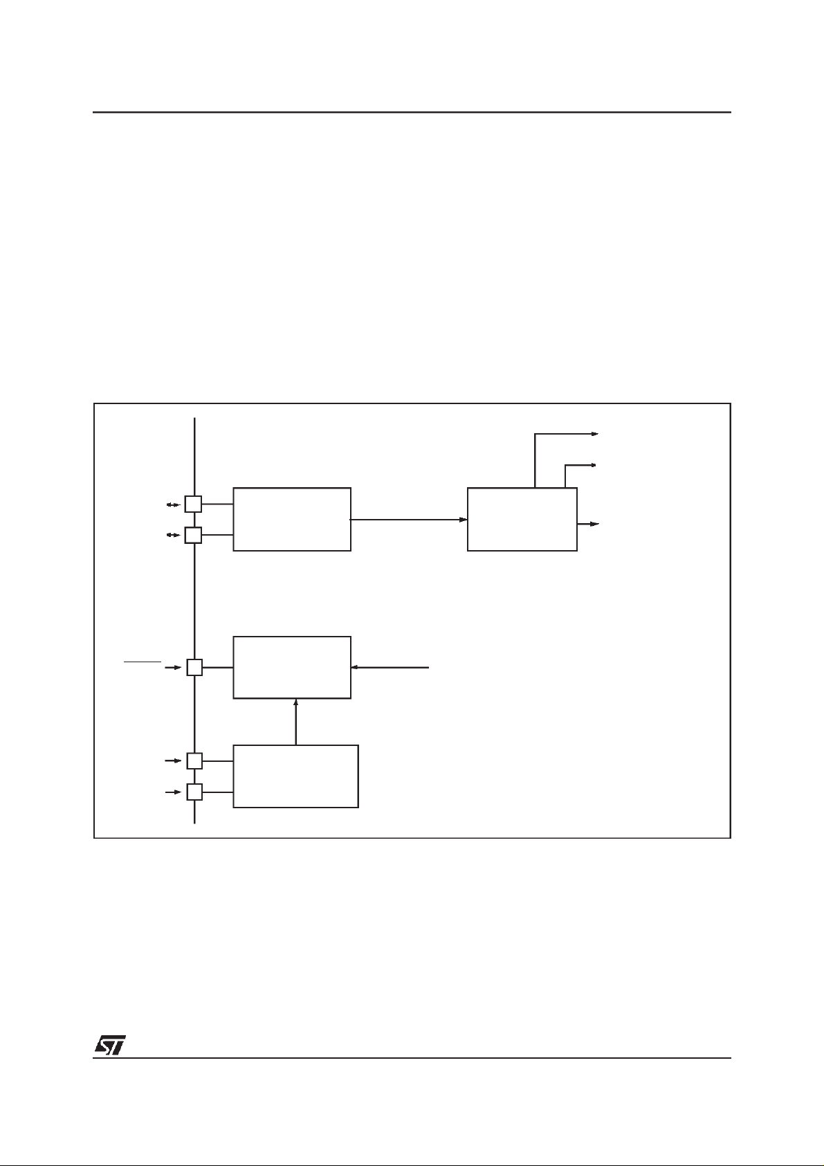
3 SUPPLY, RESET AND CLOCK MANAGEMENT
The ST72141K includes a range of utility features
for securing the application in critical situations(for
example in case of a power brown-out), and reducing the number of external components. An
overview is shown in Figure 9.
Main Features
■ Main supply low voltage detection (LVD)
■ RESET Manager
■ Low consumption resonator oscillator
■ Main clock controller (MCC)
Figure 9. Clock, RESET, Option and Supply Management Overview
ST72141K
f
MOTOR_CONTROL
f
SPI
OSC2
OSC1
RESET
V
DD
V
SS
OSCILLATOR
RESET
LOW VOLTAGE
DETECTOR
(LVD)
f
OSC
MAIN CLOCK
CONTROLLER
FROM
WATCHDOG
PERIPHERAL
(MCC)
f
CPU
17/132

ST72141K
3.1 LOW VOLTAGE DETECTOR (LVD)
To allow the integration of power management
features in the application, the Low Voltage Detector function (LVD) generates a static reset when
the VDDsupply voltage is below a V
value. This means that it secures the power-up as
LVDf
reference
well as the power-down keeping the ST7 in reset.
The V
lower than the V
reference value for a voltage drop is
LVDf
reference value for power-on
LVDr
in order to avoid a parasitic reset when the MCU
starts running and sinks current on the supply
(hysteresis).
The LVD Reset circuitry generates a reset when
VDDis below:
–V
–V
when VDDis rising
LVDr
when VDDis falling
LVDf
The LVD function is illustrated in Figure 10.
Figure 10. Low Voltage Detector vs Reset
V
DD
V
LVDr
V
LVDf
Provided the minimum VDDvalue (guaranteed for
the oscillator frequency) is below V
, the MCU
LVDf
can only be in two modes:
– under full software control
– in static safe reset
In these conditions, secure operation is always ensured for the application without the need for external reset hardware.
During aLow Voltage Detector Reset, the RESET
pin is held low, thus permitting the MCU to reset
other devices.
Notes:
The LVDallows the device to be used without any
external RESET circuitry.
HYSTERISIS
V
LVDhyst
RESET
18/132

3.2 RESET MANAGER
ST72141K
The RESET block includes three RESET sources
as shown in Figure 11:
■ ExternalRESET source pulse
■ Internal LVD RESET (Low Voltage Detection)
■ Internal WATCHDOG RESET
Figure 11. Reset Block Diagram
V
RESET
DD
R
ON
f
CPU
The RESET service routine vector is fixed at addresses FFFEh-FFFFh in theST7 memory map.
A 4096 CPUclock cycle delay allows the oscillator
to stabilise and ensures that recovery has taken
place from the Reset state.
The RESET vector fetch phase duration is 2 clock
cycles.
INTERNAL
RESET
COUNTER
WATCHDOG RESET
LVD RESET
19/132

ST72141K
RESET MANAGER (Cont’d)
External RESET pin
The RESETpin is both an input andan open-drain
output with integrated RONweak pull-up resistor
(see Figure11). This pull-up has no fixedvalue but
varies in accordance with the input voltage. Itcan
be pulled low by external circuitry to reset the device.
A RESET signal originating from an external
source must have a duration of at least t
PULSE
in
order to be recognized. Two RESET sequences
can be associated with this RESET source as
shown in Figure 12.
When the RESET is generated by a internal
source, during the two first phases of the RESET
sequence, the device RESET pin acts as an output that ispulled low.
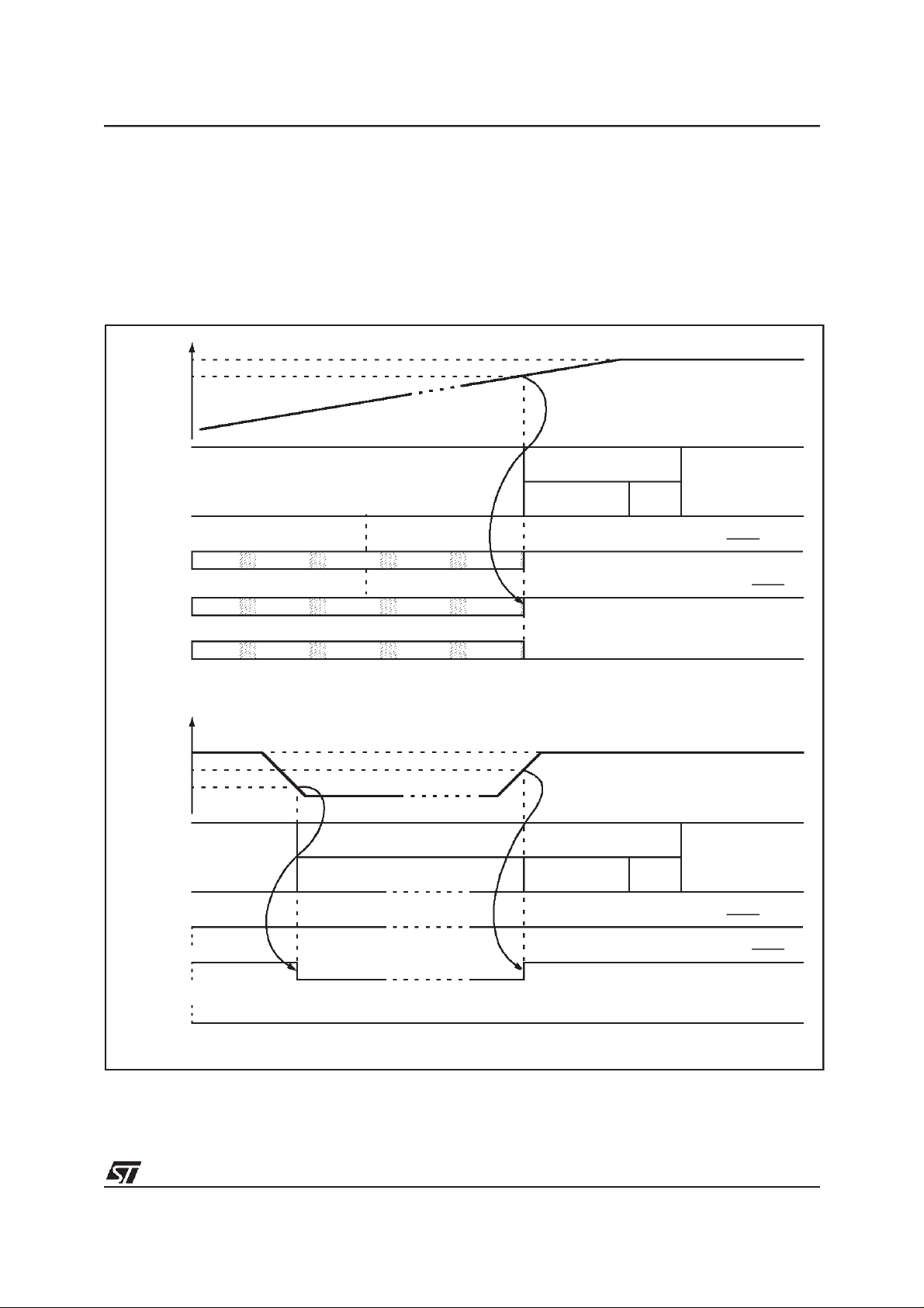
Generic Power On RESET
The function of the POR circuit consists of waking
up the MCU by detecting (at around 2V) a dynamic
(rising edge) variation of the VDDSupply. At the
beginning of this sequence, the MCU is configured
in the RESET state. When the power supply voltage rises toa sufficient level, the oscillator starts to
operate, whereupon an internal 4096 CPU cycles
delay is initiated, in order to allow the oscillator to
fully stabilize before executing the first instruction.
The initialization sequence is executed immediately following the internal delay.
To ensure correct start-up, the user should take
care that the VDD Supply is stabilized at a sufficient level forthe chosen frequency (seeElectrical
Characteristics) before the reset signal is released. In addition, supply rising must start from
0V.
As a consequence, the POR does not allow to supervise static, slowly rising, or falling, or noisy (oscillating) VDDsupplies.
An external RC network connected to the RESET
pin, or the LVD reset can be used instead to get
the best performance.
Figure 12. External RESET Sequences
V
DD
V
DD nominal
V
LVDf
RUN
t
DELAY
PULSE
INTERNAL RESET
4096 CLOCK CYCLES
RESET
FETCH
VECTOR
RUN
EXTERNAL RESET SOURCE
RESET PIN
WATCHDOG RESET
20/132
RESET MANAGER (Cont’d)
ST72141K
Internal Low VoltageDetection RESET (option)
Two different RESET sequences caused by the internal LVD circuitry can be distinguished:
- LVD Power-On RESET
- Voltage Drop RESET
Figure 13. LVD RESET Sequences
V
V
DDnominal
V
LVDr
LVD POWER-ON RESET
DD
POWER-
OFF
In the second sequence, a “delay” phase is used
to keep the device in RESET state until VDDrises
up to V
(see Figure 13).
LVDr
RESET
INTERNAL RESET
4096 CLOCK CYCLES
FETCH
VECTOR
EXTERNAL RESET SOURCE
WATCHDOG RESET
RUN
RESET PIN
V
DDnominal
V
LVDr
V
LVDf
VOLTAGE DROP RESET
V
DD
RESET
RUN
DELAY
INTERNAL RESET
4096 CLOCK CYCLES
FETCH
VECTOR
EXTERNAL RESET SOURCE
RUN
RESET PIN
WATCHDOG RESET
21/132

ST72141K
RESET MANAGER (Cont’d)
Internal Watchdog RESET
The RESET sequence generated by a internal
Watchdog counter overflow has the shortest reset
phase (see Figure 14).
Figure 14. Watchdog RESET Sequence
V
DD
V
DDnominal
V
LVDf
RESET
RUN
INTERNAL RESET
4096 CLOCK CYCLES
t
WDGRST
FETCH
VECTOR
RUN
EXTERNAL RESET SOURCE
RESET PIN
WATCHDOG UNDERFLOW
WATCHDOG RESET
22/132
3.3 LOW CONSUMPTION OSCILLATOR
ST72141K
The main clock of the ST7 can be generated by
two differentsources:
■ an external source
■ a crystal or ceramic resonator oscillators
External Clock Source
In this mode, asquare clock signal with ~50% duty
cycle has to drive the OSC2 pin while the OSC1
pin is tied to VSS(see Figure 15).
Figure 15. External Clock
ST7
OSC1 OSC2
EXTERNAL
SOURCE
Crystal/Ceramic Oscillators
This oscillator (based on constant current source)
is optimized in terms of consumption and has the
advantage of producing a very accurate rate on
the main clock of the ST7.
When using this oscillator, the resonator and the
load capacitances have to be connected as shown
in Figure 16 and have to be mounted as close as
possible to the oscillator pins in order to minimize
output distortion and start-up stabilization time.
This oscillator is not stopped during the RESET
phase to avoid losing time in the oscillator start-up
phase.
Figure 16. Crystal/Ceramic Resonator
OSC1 OSC2
C
L0
ST7
LOAD
CAPACITANCES
C
L1
23/132
ST72141K
3.4 MAIN CLOCK CONTROLLER (MCC)
The MCC block supplies the clock for the ST7
CPU and its internal peripherals. It allows the
SLOW power saving mode and the Motor Contral
The XT16 bitacts on the clockof the motor control
and SPI peripherals while the SMS bit acts on the
CPU and the other peripherals.
and SPI peripheral clocks to be managed independently. The MCC functionality is controlled by
two bits of the MISCR register: SMS and XT16.
Figure 17. Main Clock Controller (MCC) Block Diagram
OSC2
OSCILLATOR
OSC1
f
OSC
DIV 2
DIV 16
DIV 2
MCC
f
CPU
----XT16
CPU CLOCK
TO CPU AND
PERIPHERALS
SMS--
4MHz
MOTOR CONTROL
PERIPHERAL
MISCR
24/132
DIV 2
4MHz
SPI
PERIPHERAL

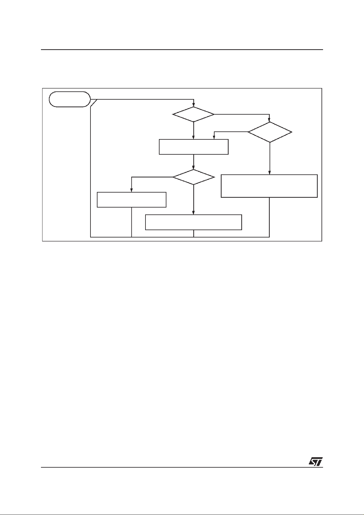
4 INTERRUPTS
ST72141K
The ST7 core may be interruptedby one oftwo different methods: maskable hardware interrupts as
listed in the Interrupt Mapping Table and a nonmaskable software interrupt (TRAP). The Interrupt
processing flowchart is shown in Figure 1.
The maskableinterrupts must be enabled clearing
the I bit in order to be serviced. However, disabled
interrupts may be latched and processed when
they are enabled (see external interrupts subsection).
When an interrupt has to be serviced:
– Normal processing is suspended at the end of
the current instruction execution.
– The PC, X, A and CC registers are saved onto
the stack.
– The I bit of the CC register is set to prevent addi-
tional interrupts.
– ThePC isthenloaded with the interrupt vectorof
the interruptto service and the first instruction of
the interrupt service routine is fetched (refer to
the Interrupt Mapping Tablefor vector addresses).
The interrupt service routine should finish with the
IRET instruction which causes the contents of the
saved registers to be recovered from thestack.
Note: As a consequence of the IRET instruction,
the I bit will be cleared and the main program will
resume.
Priority Management
By default, a servicing interrupt cannot be interrupted because the I bit is set by hardware entering in interrupt routine.
In the case when severalinterrupts are simultaneously pending, an hardware priority defines which
one will be serviced first (see the Interrupt Mapping Table).
Interrupts and Low Power Mode
All interrupts allow the processor to leave the
WAIT low power mode. Only external and specifically mentioned interrupts allow the processor to
leave the HALT low power mode (refer to the “Exit
from HALT“ column in the Interrupt Mapping Table).
4.1 NON MASKABLE SOFTWARE INTERRUPT
This interrupt is entered when the TRAP instruction is executed regardless of the stateof theI bit.
It will be serviced according to the flowchart on
Figure 1.
4.2 EXTERNAL INTERRUPTS
External interrupt vectors can be loaded into the
PC register if the corresponding external interrupt
occurred and if the I bit is cleared. Theseinterrupts
allow the processor to leave the Halt low power
mode.
The external interrupt polarity is selected through
the miscellaneous register or interrupt register (if
available).
An external interrupt triggered on edge will be
latched and the interrupt request automatically
cleared upon entering the interrupt serviceroutine.
If several input pins, connected to the same inter-
rupt vector, are configured as interrupts, their sig-
nals are logically ANDed beforeentering the edge/
level detection block.
Caution:The type of sensitivitydefinedin the Mis-
cellaneous or Interrupt register (if available) ap-
plies to the ei source. In case of an ANDedsource
(as described on the I/O ports section), a low level
on an I/O pin configured as input with interrupt,
masks the interrupt requesteven in case of rising-
edge sensitivity.
4.3 PERIPHERAL INTERRUPTS
Different peripheral interrupt flags in the status
register are able to cause an interrupt when they
are active if both:
– The I bit of the CC register is cleared.
– Thecorresponding enable bit is setin thecontrol
register.
If any of these two conditions is false, the interrupt
is latched and thus remains pending.
Clearing an interrupt request is done by:
– Writing “0” to the corresponding bit in the status
register or
– Access tothe status registerwhile the flag isset
followed by a read or write of an associated register.
Note: the clearing sequence resets the internal
latch. A pending interrupt (i.e. waiting for being en-
abled) will therefore be lost ifthe clear sequence is
executed.
25/132
ST72141K
INTERRUPTS (Cont’d)
Figure 18. Interrupt Processing Flowchart
FROM RESET
EXECUTEINSTRUCTION
RESTORE PC,X, A,CC FROM STACK
I BIT SET?
Y
FETCH NEXT INSTRUCTION
N
THIS CLEARS I BIT BY DEFAULT
IRET?
Y
N
N
INTERRUPT
PENDING?
Y
STACK PC, X, A, CC
SET I BIT
LOAD PC FROM INTERRUPT VECTOR
26/132

INTERRUPTS (Cont’d)
Table 4. Interrupt Mapping
ST72141K
N°
0 Not used FFFAh-FFFBh
1 EI0 External Interrupt Port A7..0 (C5..0*)
2 EI1 External Interrupt Port B7..0 (C5..0*) yes FFF8h-FFF9h
3
4 Motor Control Interrupt (events: C, D) no FFF2h-FFF3h
5 Motor Control Interrupt (events: E, O) no FFF0h-FFF1h
6 SPI SPI Peripheral Interrupts SPISR no FFEEh-FFEFh
7 TIMER A TIMER A Peripheral Interrupts TASR no FFECh-FFEDh
8 TIMER B TIMER B Peripheral Interrupts TBSR no FFEAh-FFEBh
9 Not used FFE8h-FFE9h
10 Not used FFE6h-FFE7h
11 Not used FFE4h-FFE5h
12 Not Used FFE2h-FFE3h
13 Not Used FFE0h-FFE1h
Source
Block
RESET Reset
TRAP Software Interrupt no FFFCh-FFFDh
Motor Control Interrupt (events: R, Z)
MTC
Description
Register
Label
N/A
N/A
MISR
Priority
Order
Highest
Priority
Lowest
Priority
Exit
from
HALT
yes FFFEh-FFFFh
yes FFFAh-FFFBh
no FFF4h-FFF5h
Address
Vector
27/132

ST72141K
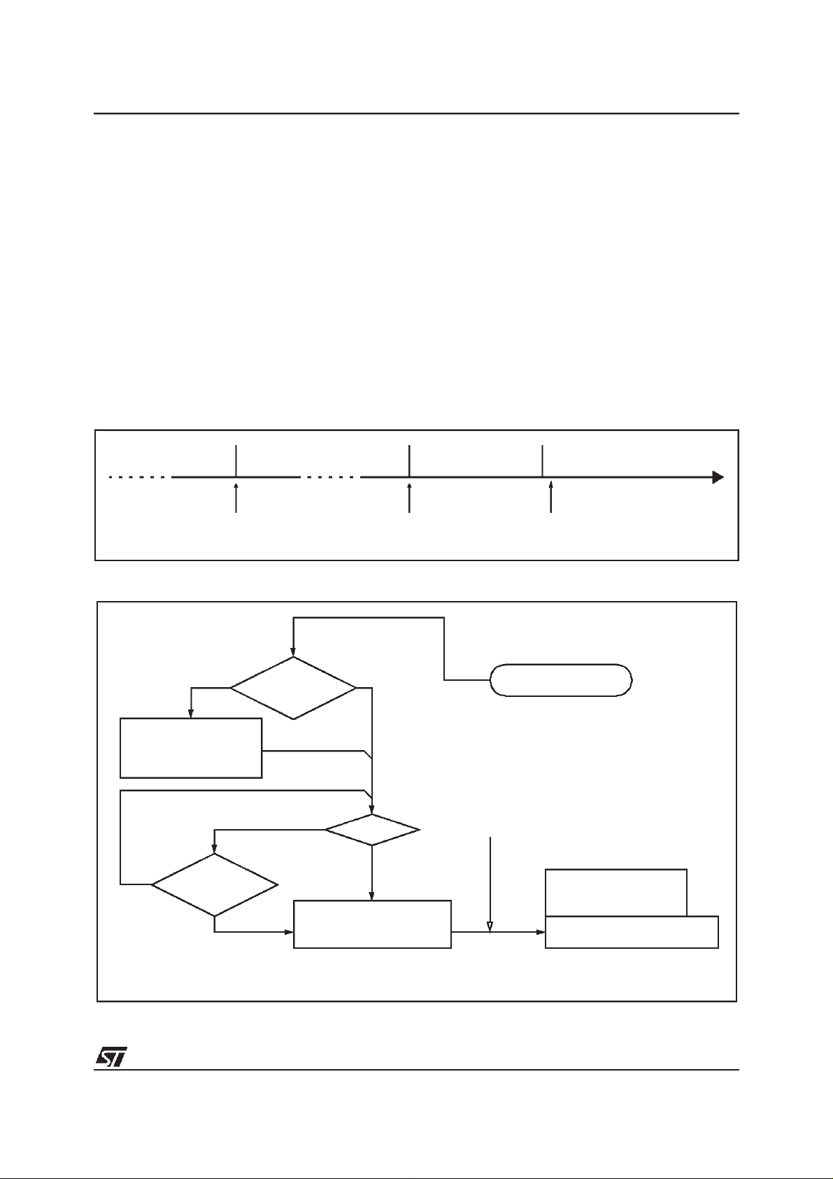
5 POWER SAVING MODES
5.1 Introduction
To give a large measure of flexibilitytotheapplication in terms of power consumption, three main
power saving modes are implemented in the ST7
(see Figure 19).
After a RESET the normal operating mode is selected by default (RUN mode). This mode drives
the device (CPU and embedded peripherals) by
means of a master clock which is based on the
main oscillator frequency divided by 2 (f
From Run mode, the different power saving
modes may be selected by setting the relevant
register bits or by calling the specific ST7 software
instruction whose action depends on the the oscillator status.
Figure 19. Power saving mode consumption / transitions
CPU
).
Low
POWERCONSUMPTION
SLOW WAIT
WAIT SLOW RUNHALT
High
28/132
POWER SAVING MODES (Cont’d)
5.2 HALT Mode
The HALT mode is the lowest power consumption
mode of the MCU. It is entered by executing the
ST7 HALT instruction (see Figure 21).
The MCU can exit HALT mode on reception of either an external interrupt or a reset (see Table 2).
When exiting HALT mode by means of a RESET
or an interrupt, the oscillator is immediately turned
on and the 4096 CPU cycle delay is used to stabilize theoscillator. After the start up delay, the CPU
resumes operation by servicing the interrupt or by
fetching the reset vector which woke it up(see Figure 20).
Figure 20. HALT Mode timing overview
ST72141K
When entering HALT mode, the I bit in the CC
Register is forced to 0 to enable interrupts.
In the HALT mode the main oscillator is turned off
causing all internal processing to be stopped, including the operation of the on-chip peripherals.
All peripherals are not clocked except the ones
which get their clock supply from another clock
generator (such as an external or auxiliary oscillator).
RUN
HALT
HALT
INSTRUCTION
Figure 21. HALT modes flow-chart
WATCHDOG
HALT
OSCILLATOR
PERIPHERALS
CPU
I BIT
N
EXTERNAL*
INTERRUPT
Y
ENABLE
OFF
OFF
OFF
0
N
OSCILLATOR
PERIPHERALS
CPU
RESET
INTERRUPT
YN
RESET
Y
4096 CPU CYCLE
DELAY
OR
ON
OFF
OFF
FETCH
VECTOR
HALT INSTRUCTION
4096 clock cycles delay
OSCILLATOR
PERIPHERALS
CPU
FETCH RESET VECTOR
OR SERVICE INTERRUPT **
RUN
ON
ON
ON
Notes:
External interrupt or internal interrupts with Exit from Halt Mode capability
*
Before servicing an interrupt, the CC register is pushed on the stack.
**
29/132

ST72141K
POWER SAVING MODES (Cont’d)
5.3 WAIT Mode
WAIT mode places the MCU in a low power consumption mode by stopping the CPU.
This power saving mode is selectedby calling the
“WFI” ST7 software instruction.
All peripherals remain active. During WAIT mode,
the I bit of the CC register are forced to 0, to enable all interrupts. All other registers and memory
remain unchanged. The MCU remains in WAIT
mode until an interrupt or Reset occurs, whereupon the Program Counter branches to the starting
address of the interrupt or Reset serviceroutine.
The MCU will remain in WAIT mode until a Reset
or an Interrupt occurs, causing it to wake up.
Refer to Figure22.
Figure 22. WAIT mode flow-chart
OSCILLATOR
WFI INSTRUCTION
PERIPHERALS
CPU
I BIT
5.4 SLOW Mode
This mode has two targets:
– To reduce powerconsumption bydecreasingthe
internal clock in the device,
– To adapt the internal clock frequency (f
CPU
)to
the available supply voltage.
SLOW mode is controlled by the SMS bit in the
MISCR register. This bit enables or disables Slow
mode selecting the internal slow frequency (f
CPU
In this mode, the oscillator frequency can bedivided by 32 instead of 2 in normal operating mode.
The CPU and peripheralsare clocked atthis lower
frequency except the Motor Control and the SPI
peripherals which have their own clock selection
bit (XT16) in the MISCR register.
ON
ON
OFF
0
).
N
Note:
N
INTERRUPT
Y
OSCILLATOR
PERIPHERALS
CPU
The peripheral clock is stopped only when exit caused by RESET and not by an interrupt.
*
Before servicing an interrupt, the CC register is pushed on the stack.
**
RESET
Y
ON
OFF*
OFF
if exit caused by a RESET, a 4096 CPU
clock cycle delay is inserted.
OSCILLATOR
PERIPHERALS
CPU
ON
ON
ON
FETCH RESET VECTOR
OR SERVICE INTERRUPT**
30/132
 Loading...