

SGS Thomson Microelectronics ST72T85A5Q6, ST72E85A5G0, ST7285C, ST7285A5CQ8, ST7285A5CQ6 Datasheet
...
November 1997 1/117
R
Rev. 1.0
ST7285C
8-BIT MCU FOR RDS WITH 48K ROM, 3K RAM, ADC,
TWO TIMERS, TWO SPIs, I
2
C AND SCI INTERFACES
■
4.5V to 5.5V Supply Operating Range
■ Operates at 8.664MHz Oscillator Frequency for
RDS compatibility
■
Fully Static operation
■
-40°Cto+85°C Maximum Operating
Temperature Range
■
Run, Wait, Slow, Halt and RAM Retention
modes
■
User ROM: 48 Kbytes
■ Data RAM: 3 Kbytes, including 128 byte stack
■
80 pin plastic package
■
62 multifunctional bidirectional I/O lines:
– Programmable Interrupt inputs on some I/Os
– 8 Analog inputs
– EMI filtering
■
Two 16-bit Timers, each featuring:
– 2 Input Captures
– 2 Output Compares
– External Clock input (on Timer A)
– PWM and Pulse Generator modes
■ RDS Radio Data System Filter, Demodulator
and GBS circuits
■
8-bit Analog-to-Digital converter with 8 channel
analog multiplexer
■ Digital Watchdog
■
Two SPI Serial Peripheral Interfaces
■
SCI Serial Communications Interface
■ Full I
2
C multiple Master/Slave interface
■ 2KHz Beep signal generator
■
Master Reset and Power-On Reset
■
8-bit Data Manipulation
■ 63 Basic Instructions
■
17 main Addressing Modes
■
8 x 8 Unsigned Multiply Instruction
■ True Bit Manipulation
■ Complete Development Support on PC/DOS/
WindowsTMReal-Time Emulator
■
Full Software Package (C-Compiler, CrossAssembler, Debugger)
PQFP80
1

2/117
Table of Contents
117
ST7285C . . . . . . . . . . . . . . . . . . . . . . . . . . . . . . . . . . . . . . . . . . . .1
1 GENERAL DESCRIPTION . . . . . . . ...............................................5
1.1 INTRODUCTION .........................................................5
1.2 PIN DESCRIPTION .......................................................6
1.3 MEMORYMAP .........................................................10
2 CENTRAL PROCESSING UNIT .................................................13
2.1 INTRODUCTION ........................................................13
2.2 CPU REGISTERS . . . . . . . . ...............................................13
3 CLOCKS, RESET, INTERRUPTS & POWER SAVING MODES ........................15
3.1 CLOCKSYSTEM........................................................15
3.1.1 General Description .................................................15
3.1.2 Crystal Resonator . . . . . . . . ..........................................15
3.1.3 Ceramic Resonator . . . ..............................................16
3.1.4 External Clock . . . . . . . ..............................................16
3.2 MISCELLANEOUS REGISTER . . . . . . . . . . . . . . . . . . . . . . . . . . . . . ................17
3.3 RESETS...............................................................18
3.3.1 Introduction . . . . . . . . ...............................................18
3.3.2 External Reset . . . . . . . . . . ...........................................18
3.3.3 Reset Operation . . . . . . . . . . . . . . . .....................................18
3.3.4 Power-on Reset . . . . . . . . . . . . . . . .....................................18
3.4 WATCHDOG TIMER SYSTEM (WDG) . . .....................................19
3.4.1 Introduction . . . . . . . . ...............................................19
3.4.2 Functional Description . . . ............................................19
3.4.3 Watchdog Register . . . ..............................................19
3.5 INTERRUPTS . . . . ......................................................20
3.6 POWER SAVING MODES .................................................22
3.6.1 SlowMode........................................................22
3.6.2 WaitMode ........................................................22
3.6.3 HaltMode.........................................................23
4 ON-CHIP PERIPHERALS . . . ...................................................24
4.1 I/OPORTS.............................................................24
4.1.1 Introduction . . . . . . . . ...............................................24
4.1.2 Generic I/O Features . . . . . . . . . . . . . . . . . . . . . . . . . . . . . . . . ................24
4.1.3 I/O Port Implementation . . . . . . . . . . . . ..................................27
4.2 SERIAL COMMUNICATIONS INTERFACE. . ..................................28
4.2.1 Introduction . . . . . . . . ...............................................28
4.2.2 Features . . . . . . . . . . . . . . . ...........................................28
4.2.3 Serial Data Format . .................................................28
4.2.4 Data Reception and Transmission. . . ...................................28
4.2.5 Receiver Muting and Wake-up Feature . . . . ..............................28
4.2.6 Baud Rate Generation . . . ............................................29
4.2.7 SCI Register Overview . . . ............................................29
4.3 16-BIT TIMER . . . . ......................................................35
4.3.1 Introduction . . . . . . . . ...............................................35
4.3.2 Counter . . . . ......................................................35

3/117
Table of Contents
4.3.3 External Clock . . . . . . . ..............................................37
4.3.4 Input Capture . . . ...................................................39
4.3.5 Output Compare . . . . ...............................................40
4.3.6 Timer Registers . . . . . . . . . . . . . . . . . . . . . . . . . . . .........................43
4.4 SERIAL PERIPHERAL INTERFACE . . . . . . . . . . . . . . . . . . . . .....................45
4.4.1 Introduction . . . . . . . . ...............................................45
4.4.2 Features . . . . . . . . . . . . . . . ...........................................45
4.4.3 Functional Description . . . ............................................45
4.4.4 Signal Description . . . . . . . . ..........................................47
4.4.5 Master Out Slave In (MOSI). ..........................................47
4.4.6 Master In Slave Out (MISO) . ..........................................47
4.4.7 Serial Peripheral Control Register (SPCR) ...............................50
4.4.8 Serial Peripheral Status Register (SPSR) . . . . . ...........................51
4.4.9 Serial Peripheral Data I/O Register (SPDR) . . . . . .........................53
4.4.10Single Master And Multimaster Configurations . . . . ........................53
4.5 I2C BUS INTERFACE . . . . . . . . . . . . . . . . . . . . . . . . . . . .........................54
4.5.1 Introduction . . . . . . . . ...............................................54
4.5.2 General Features . . . . ...............................................54
4.5.3 Functional Description . . . ............................................54
4.5.4 EPROM/ROM I C COMPATIBILITY APPLICATION NOTE. . . . ...............56
4.5.5 Re giste r Desc ript ion .................................................57
4.5.6 I2C Stat e Machine: . . . ..............................................61
4.6 A /D CONVERTER (ADC) . .................................................64
4.6.1 Introduction . . . . . . . . ...............................................64
4.6.2 Fu nctio nal De scrip tion . . . ............................................64
4.6.3 Re giste r Desc ript ion .................................................65
4.7 RDS FILTER . . . ........................................................66
4.7.1 Fe atures . . . . . . . . . . . . . . . ...........................................66
4.7.2 Fu nctio nal De scrip tion . . . ............................................67
4.8 RDS DEMODULATOR . . . . . . . . . . . . . . . .....................................68
4.8.1 Fe atures . . . . . . . . . . . . . . . ...........................................68
4.8.2 Fu nctio nal De scrip tion . . . ............................................69
4.9 RDSG.B.S.............................................................72
4.9.1 Introduction . . . . . . . . ...............................................72
4.9.2 Fe atures . . . . . . . . . . . . . . . ...........................................72
4.9.3 Fu nctio nal De scrip tion . . . ............................................74
4.9.4 Ac quisition of Group and Block Synchronization . . . . .......................77
4.9.5 Application Tips . . . . . . . . . . . . . . . . . . . . . . . . . . . .........................77
4.9.6 Block Synchronization Software . . .....................................77
4.9.7 Error Correction s oftwar e . . . . . . . . . . . . . . . . . . . . . . . . . . . . . ................77
5SOFTWARE ................................................................78
5.1 S T7 ARCHITECTU RE . . . . . . . . . . . . . . . .....................................78
5.2 S T7 ADDRESSING MOD ES ...............................................78
5.3 S T7 INSTRUCT ION SET . .................................................83
6 EL ECT RICAL CHARACTERI STI CS. . . . . . . . . . . . ..................................86
6.1 A BSO LUT E M AXIMUM RATINGS. ..........................................86
6.2 P OWER CONSID ERATIONS . . . . ..........................................87

4/117
Table of Contents
117
6.3 DC ELECTRICAL CHARACTERISTICS ......................................88
6.4 AC ELECTRICAL CHARACTERISTICS ......................................89
6.5 CONTROLTIMING ......................................................89
7 GENERAL INFORMATION . . . . . . . . . . ...........................................96
7.1 PACKAGE MECHANICAL DATA. . . . ........................................96
ST72E85
ST72T85 . . . . . . . . . . . . . . . . . . . . . . . . . . . . . . . . . . . . . . . . . . .97
1 GENERAL DESCRIPTION. . . ...................................................98
1.1 INTRODUCTION ........................................................98
1.2 PIN DESCRIPTION ......................................................99
1.3 MEMORYMAP.........................................................103
1.4 EPROM ERASURE .....................................................105
1.5 EPROM/R OM I C COMPATIBILITY APPLICATION NOTE.......................106
2 ELECTRICAL CHARACTERISTI CS. . . . .........................................107
2.1 ABSOLUTE MAXIMUM RATINGS. . . . . . ....................................107
2.2 POWER CONSIDERATIONS. . . ...........................................108
2.3 DC ELECTRICAL CHARACTERISTICS .....................................109
2.4 AC ELECTRICAL CHARACTERIS TICS. . . ...................................110
2.5 CONTROLTIMING......................................................110
3 GENERAL INFORMATION . . . . . . . . . . ..........................................117
3.1 PACKAGE MECHANICAL DATA. . . . .......................................117
5/117
ST7285C
1 GENERAL DESCRIPTION
1.1 INTRODUCTION
The ST7285C HCMOS Microcontroller Unit is a
member of the ST7 family of Microcontrollers dedicated to car radio applications with RDS capability. The device is based on an industry-standard 8bit core and features an enhanced instruction set.
The device is normally operated at an 8.664MHz
oscillator frequency for RDS compatibility but,
thanks to the fully static design, operation is possible down to DC, when RDS functionality is not required. Under software control, theST7285C may
be placed in either WAIT, SLOW or HALT modes,
thus reducing power consumption. The enhanced
instruction set and addressing modes afford real
programming potential. In addition to standard 8bit data management, theST7285C features true
bit manipulation, 8x8 unsigned multiplication and
indirect addressing modes.
The device includes an on-chip oscillator, CPU,
ROM, RAM, 62 I/O lines and the following on-chip
peripherals: Analog-to-Digital converter (ADC),
two industry standard SPI serial interfaces, a Serial Communications Interface, an I2C interface, a
digital Watchdog Timer, two independent 16-bit
Timers, one featuring an External Clock Input, and
both featuring Pulse Generator capabilities, 2 Input Captures and 2 Output Compares. RDS Filter,
Demodulator and GBS circuitry for car radio applications is also included.
NOTE
:
FOR THIS DEVICE, SGS-THOMSON
CAN ONLY RECEIVE MOTOROLA S19 FORMAT
FOR ROM CODES.
Figure 1. ST7285C Block Diagram
*On EPROM or OTP versions only.
Power on Reset
PA0 - PA7
Pin 65..72
PB0 - PB7
Pin 73..80
OSCin
OSCout
RESET
V
PP
/ TEST
OSC
8 -BIT CORE
ALU
VR01735P
Internal
CLOCK
ADDRESSand DATA BUS
TimerA
PORT A
PORT B
A/D Converter
8
4
SPI B
PORT C
PC0 - PC7
Pin 5..12
SPI A
PORT D
I
2
C
SCI
8
RAM
3k
RDS
FILTER,DEMOD,GBS
8
8
8
TimerB
4
4
2
PD0 - PD7
Pin 13..20
2
PORT E
PE0 - PE7
Pin 25..32
8
PORT F
PF0 - PF7
Pin 33..40
8
PORT H
PORT G
PH0 - PH5
Pin 53..58
6
PG0 - PG7
Pin 45..52
8
ROMor EPROM*
48k
Watchdog
RDScomp
MPX
RDS fil
RDS ref
ARS
AINT
V
DD
V
SS
V
DDPVSSPVDDAVSSA
2
2
6/117
ST7285C
1.2 PIN DESCRIPTION
All I/Os from Port A to Port D, as well as PH0, 1
and 2, feature alternate function compatibility.
Software selectable input pull-ups are available on
ports featuring interrupt capability (PC4, PC5,
PD4, PD5, PF0-PF3, PG3).
VSSA
VDDA
MPX
RDSREF
RDSFIL
RDSCOMP
PH5
PH4
PH3
PH2/RDSDATA
PH1/RDSCLKOUT
PH0/RDSQUAL
PG7
PG6
PG5
PG4
PG3
PG2
PG1
PG0
ARS
AINT
VDDP
VSSP
VSSP
VDDP
OSCOUT
OSCIN
PC0/MISO_B
PC1/MOSI_B
PC2/SCK_B
PC3/SS_B
PC4/OC2_B
PC5/OC1_B
PC6/IC2_B
PC7/IC1_B
PD0/MISO_A
PD1/MOSI_A
PD2/SCK_A
PD3/SS_A
PD4
PD5
PD6/SCL
PD7/SDA
RESET
VPP*/TEST
VDD
VSS
1
2
3
4
5
6
7
8
9 (I10)
10 (I10)
11
12
13
14
15
16
17 (I9)
18 (I9)
19
20
21
22
23
24
64
63
62
61
60
59
58
57
56
55
54
53
52
51
50
49
(I1) 48
47
46
45
44
43
42
41
80 79 78 77 76 75 74 73 72 71 70 69 68 67 66 65
25 26 27 28 29 30 31 32 37 38 39
40
PB7/BEEP/
CLKOUT
PB6/CLKEXT
PB5/OC2_A
PB4/OC1_A
PB3/IC2_A
PB2/IC1_A
PB1/RDI
PB0/TDO
PA7/AIN7
PA6/AIN6
PA5/AIN5
PA4/AIN4
PA3/AIN3
PA2/AIN2
PA1/AIN1
PA0/AIN0
PE0
PE1
PE2
PE3
PE4
PE5
PE6
PE7
PF0
PF1
PF2
PF3
PF4
PF5
PF6
PF7
33 34 35 36
*) On EPROM/OTPversions only
(I2)(I2)(I2)(I2)
7/117
ST7285C
Pin Pin Name(s) Basic Function Alternate Function Remarks
1V
SSP
Ground for Output Buffers
-
This pin is connected to pin 41
2V
DDP
Power Supply for Output Buffers
This pin is connected to pin 42
3 OSCOUT Oscillator Output pin.
4 OSCIN Oscillator Input pin.
5 PC0/MISO_B I/O Port PC0
SPI B master in/slave
out data input/output
Alternate function or I/O. The I/O configuration
is software selectable as triggered input or
push pull output.
6 PC1/MOSI_B I/O Port PC1
SPI B Master Out/
Slave In Data Input/
Output
7 PC2/SCK_B I/O Port PC2 SPI B Serial Clock
8 PC3/SS_B I/O Port PC3 SPI B Slave Select
9 PC4/OC2_B I/O Port PC4
Output Compare 2
on Timer B
Alternate function or I/O. Software selectable
as triggered input, push pull output, or triggered interrupt input with pull up (Interrupt I10).
10 PC5/OC1_B I/O Port PC5
Output Compare 1
on Timer B
11 PC6/IC2_B I/O Port PC6
Input Capture 2
on Timer B
Alternate function or I/O. The I/O configuration
is software selectable as triggered input or
push pull output.
12 PC7/IC1_B I/O Port PC7
Input Capture 1
on Timer B.
13 PD0/MISO_A I/O Port PD0
SPI A Master In/Slave
Out Data Input/Output
14 PD1/MOSI_A I/O Port PD1
SPI A Master Out/
Slave In data Input/
Output
15 PD2/SCK_A I/O Port PD2 SPI A Serial Clock
16 PD3/SS_A I/O Port PD3 SPI A Slave Select
17 PD4 I/O Port PD4 - Software selectable as triggered input, push
pull output, open drain output or triggered interrupt input with pull up (Interrupt I9).
18 PD5 I/O Port PD5 19 PD6/SCL I/O Port PD6 I
2
C Serial Clock Alternate function or I/O. The I/O configuration
is software selectable as triggered input or
open drain output.
20 PD7/SDA I/O Port PD7 I
2
C Serial Data
21 RESET General Reset -
Bidirectional. An active low signal forces MCU
initialization. This event is the top priority nonmaskable interrupt. As an output, it can be
used to reset external peripherals.
22 TEST RESERVED -
Input. This pin MUST be tied directly to V
SS
during normal operation.
23 V
DD
Power Supply forall logic circuitry
Except for output buffers and pull-ups.
24 V
SS
Ground for all logic circuitry
-
25 PE0 I/O Port PE0 -
Software selectable as triggered input or push
pull output.
26 PE1 I/O Port PE1 27 PE2 I/O Port PE2 28 PE3 I/O Port PE3 29 PE4 I/O Port PE4 30 PE5 I/O Port PE5 31 PE6 I/O Port PE6 32 PE7 I/O Port PE7 -
8/117
ST7285C
33 PF0 I/O Port PF0 -
Software selectable as triggered input, a push
pull output, open drain output, or triggered interrupt input with pull up (Interrupt I2).
34 PF1 I/O Port PF1 35 PF2 I/O Port PF2 36 PF3 I/O Port PF3 37 PF4 I/O Port PF4 -
Software selectable as a triggered input or as
a push pull output.
38 PF5 I/O Port PF5 39 PF6 I/O Port PF6 40 PF7 I/O Port PF7 -
41 V
SSP
Ground for Output Buffers.
- This pin is connected to pin 1.
42 V
DDP
Power Supply for Output Buffers
- This pin is connected to pin 2.
43 AINT Reserved - Must be tied to 5V
44 ARS Reserved - Must be tied to 5V
45 PG0 I/O Port PG0 -
Software selectable as triggered input or push
pull output.
46 PG1 I/O Port PG1 47 PG2 I/O Port PG2 -
48 PG3 I/O Port PG3 -
Software selectable as triggered input, a push
pull output, open drain output, or triggered interrupt input with pull up (Interrupt I1).
49 PG4 I/O Port PG4 -
Software selectable as triggered input or push
pull output. Note that PH0, 1, 2 offer alternate
function capabilities for test purposes.
50 PG5 I/O Port PG5 51 PG6 I/O Port PG6 52 PG7 I/O Port PG7 -
53
PH0/
RDSQUAL
I/O Port PH0 RDS Quality signal
54
PH1/
RDSCLKOUT
I/O Port PH1
RDS GBS Clock Out
signal
55
PH2/
RDSDATA
I/O Port PH2 RDS GBS Data signal
56 PH3 I/O Port PH3 -
Software selectable as triggered input or high
voltage (10V max) open drain output.
57 PH4 I/O Port PH4 58 PH5 I/O Port PH5 -
59 RDSCOMP RDS Comp Input signal
Used to feed theDemodulator froman external
filter when the internal filter is switched off.
60 RDSFIL
RDS Filtered Output
signal
Used for Demodulator test purposes.
61 RDSREF RDS Input Reference
62 MPX RDS input signal
63 V
DDA
Analog Power Supply
For RDS and ADC circuits
64 V
SSA
Analog Ground
65 PA0/AIN0 I/O Port PA0
Analog input to ADC
Alternate function or I/O. The I/O configuration
is software selectable as triggered input or
push pull output. Note that when a pin is used
as Analog input it must not be configured as an
output to avoid conflicts with the analog voltage to be measured.
66 PA1/AIN1 I/O Port PA1
67 PA2/AIN2 I/O Port PA2
68 PA3/AIN3 I/O Port PA3
69 PA4/AIN4 I/O Port PA4
70 PA5/AIN5 I/O Port PA5
71 PA6/AIN6 I/O Port PA6
72 PA7/AIN7 I/O Port PA7
Pin Pin Name(s) Basic Function Alternate Function Remarks
9/117
ST7285C
73 PB0/TDO I/O Port PB0
SCI Transmit Data
Out
Alternate function or I/O. The I/O configuration
is software selectable as triggered input or
push pull output.
74 PB1/RDI I/O Port PB1 SCI Receive Data In
75 PB2/IC1_A I/O Port PB2
Input capture 1
on Timer A
76 PB3/IC2_A I/O Port PB3
Input capture 2
on Timer A
77 PB4/OC1_A I/O Port PB4
Output compare 1
on Timer A
78 PB5/OC2_A I/O Port PB5
Output compare 2
on Timer A
79 PB6/CLKEXT I/O Port PB6
External Clock on
Timer A
80
PB7/BEEP/
CLKOUT
I/O Port PB7 BEEP or CPU Clock.
This pin can be a push pull output delivering
the Beep signal (2KHz) or the CPU clock, according to the miscellaneous register settings.
Pin Pin Name(s) Basic Function Alternate Function Remarks

10/117
ST7285C
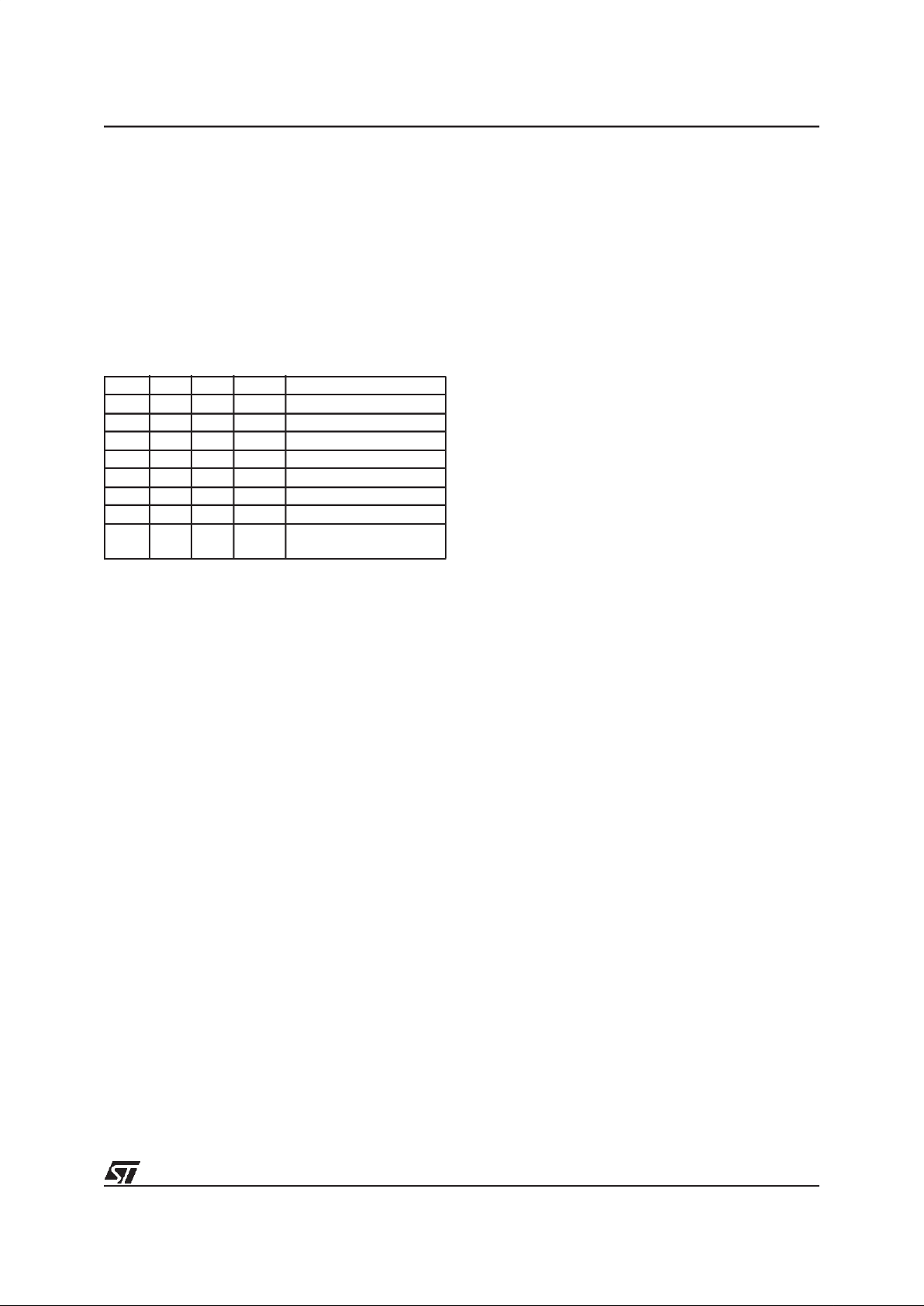
1.3 MEMORY MAP
Table 1. Memory Map
Address Block Register name
Reset
Status
Remarks
0000h
0001h
0002h
0003h
Port A
Data Reg
Data Direction Reg
Not Used
Not Used
00h
00h
R/W Register
R/W Register
Absent
Absent
0004h
0005h
0006h
0007h
Port B
Data Reg
Data Direction Reg
Not Used
Not Used
00h
00h
R/W Register
R/W Register
Absent
Absent
0008h
0009h
000Ah
000Bh
Port C
Data Reg
Data Direction Reg
Option Reg
Not Used
00h
00h
--00----b
R/W Register
R/W Register
R/W Register
Absent
000Ch
000Dh
000Eh
000Fh
Port D
Data Reg
Data Direction Reg
Option Reg
Not Used
00h
00h
--00----b
R/W Register
R/W Register
R/W Register
Absent
0010h
0011h
0012h
0013h
Port E
Data Reg
Data Direction Reg
Not Used
Not Used
00h
00h
R/W Register
R/W Register
Absent
Absent
0014h
0015h
0016h
0017h
Port F
Data Reg
Data Direction Reg
Option Reg
Not Used
00h
00h
----0000b
R/W Register
R/W Register
R/W Register
Absent
0018h
0019h
001Ah
001Bh
Port G
Data Reg
Data Direction Reg
Option Reg
Not Used
00h
00h
----0---b
R/W Register
R/W Register
R/W Register
Absent
001Ch
001Dh
001Eh
001Fh
Port H
Data Reg
Data Direction Reg
Not Used
Not Used
00h
00h
R/W Register
R/W Register
Absent
Absent
0020h
Miscellaneous Reg-
ister
00h see register description
0021h
0022h
0023h
SPI A
Data I/O Reg
Control Reg
Status Reg
XXh
0xh
00h
R/W Register
R/W Register
Read Only Register
0024h WDG Watchdog register 7Fh see register description
0025h
0026h
0027h
SPI B
Data I/O Reg
Control Reg
Status Reg
XXh
0xh
00h
R/W Register
R/W Register
Read Only Register

11/117
ST7285C
0028h
0029h
002Ah
002Bh
002Ch
002Dh
002Eh
I
2
C
CR: Control Register
SR1: Status Register 1
SR2: Status Register 2
CCR: Clock Control Register
OAR1: Own Address Register 1
OAR2: Own Address Register 2
DR: Data Register
00h
00h
00h
00h
00h
00h
00h
R/W Register
Read Only Register
Read Only Register
R/W Register
R/W Register
R/W Register
R/W Register
002Fh
0030h
RESERVED
0031h
0032h
0033h
0034h
0035h
0036h
0037h
0038h
0039h
003Ah
003Bh
003Ch
003Dh
003Eh
003Fh
Timer A
Control Reg2
Control Reg1
Status Reg
Input Capture1 High Register
Input Capture1 Low Register
Output Compare1 High Register
Output Compare1 Low Register
Counter High Register
Counter Low Register
Alternate Counter High Register
Alternate Counter Low RegisteR
Input Capture2 High Register
Input Capture2 Low Register
Output Compare2 High Register
Output Compare2 Low Register
00h
00h
XXh
XXh
XXh
XXh
XXh
FFh
FCh
00h
00h
XXh
XXh
XXh
XXh
R/W Register
R/W Register
Read Only Register
Read Only Register
Read Only Register
R/W Register
R/W Register
Read Only Register
Read Only Register
Read Only Register
Read Only Register
Read Only Register
Read Only Register
R/W Register
R/W Register
0040h RESERVED
0041h
0042h
0043h
0044h
0045h
0046h
0047h
0048h
0049h
004Ah
004Bh
004Ch
004Dh
004Eh
004Fh
Timer B
Control Reg2
Control Reg1
Status Reg
Input Capture1 High Register
Input Capture1 Low Register
Output Compare1 High Register
Output Compare1 Low Register
Counter High Register
Counter Low Register
Alternate Counter High Register
Alternate Counter Low Register
Input Capture2 High Register
Input Capture2 Low Register
Output Compare2 High Register
Output Compare2 Low Register
00h
00h
XXh
XXh
XXh
XXh
XXh
FFh
FCh
00h
00h
XXh
XXh
XXh
XXh
R/W Register
R/W Register
Read Only Register
Read Only Register
Read Only Register
R/W Register
R/W Register
Read Only Register
Read Only Register
Read Only Register
Read Only Register
Read Only Register
Read Only Register
R/W Register
R/W Register
0050h
0051h
0052h
0053h
0054h
0055h
0056h
0057h
SCI
SCI Prescaler
SCSR: Status Register
SCDR: Data Register
SCBRR: Baud Rate Register
SCCR1: Control Register 1
SCCR2: Control Register 2
PSCBRR: Receive Baud Rate Reg
Reserved
PSCBRT: Transmit Baud Rate Reg
1100000xb
XXh
00x----xb
XXh
00h
00h
---
00h
Read Only Register
R/W Register
R/W Register
R/W Register
R/W Register
R/W Register
Reserved ST use
R/W Register
0058h RESERVED
0059h RESERVED
005Ah
005Bh
RDS Filter
RDS FI1
RDS FI2
R/W Register
R/W Register
Address Block Register name
Reset
Status
Remarks

12/117
ST7285C
005Ch
005Dh
005Eh
005Fh
RDS Demodulator
RDS DE1
RDS DE2
RDS DE3
RDS DE4
see register description
0060h
0061h
0062h
0063h
0064h
0065h
0066h
0067h
0068h
0069h
006Ah
006Bh
006Ch
006Dh
006Eh
006Fh
RDS GBS
SR0 -Shift Reg 0
SR1 -Shift Reg 1
SR2 -Shift Reg 2
SR3 -Shift Reg 3
SY0 -Polynomial Reg 0
SY1 -Polynomial Reg 1
GS_CNT Count Reg
GS_INT Interrupt Reg
DR0 -RDSDAT Reg 0
DR1 -RDSDAT Reg 1
DR2 -RDSDAT Reg 2
DR3 -RDSDAT Reg 3
QR0 -QUALITY Reg 0
QR1 -QUALITY Reg 1
QR2 -QUALITY Reg 2
QR3 -QUALITY Reg 3
see register description
0070h
0071h
ADC
Data Reg
Control/Status Reg
XXh
00h
Read Only Register
R/W Register
0072h to
007Fh
RESERVED
0080h to
0BFFh
0C00h to
0C7Fh
RAM 3K Bytes
of which
STACK 128 Bytes
User variables and subroutine nesting
0C80h to
3FFFh
RESERVED
4000h to
FFDFh
ROM 48K bytes
(49120 bytes)
User application code and data
FFE0h to
FFFFh
User vectors Interrupt and Reset Vectors
Address Block Register name
Reset
Status
Remarks
13/117
ST7285C
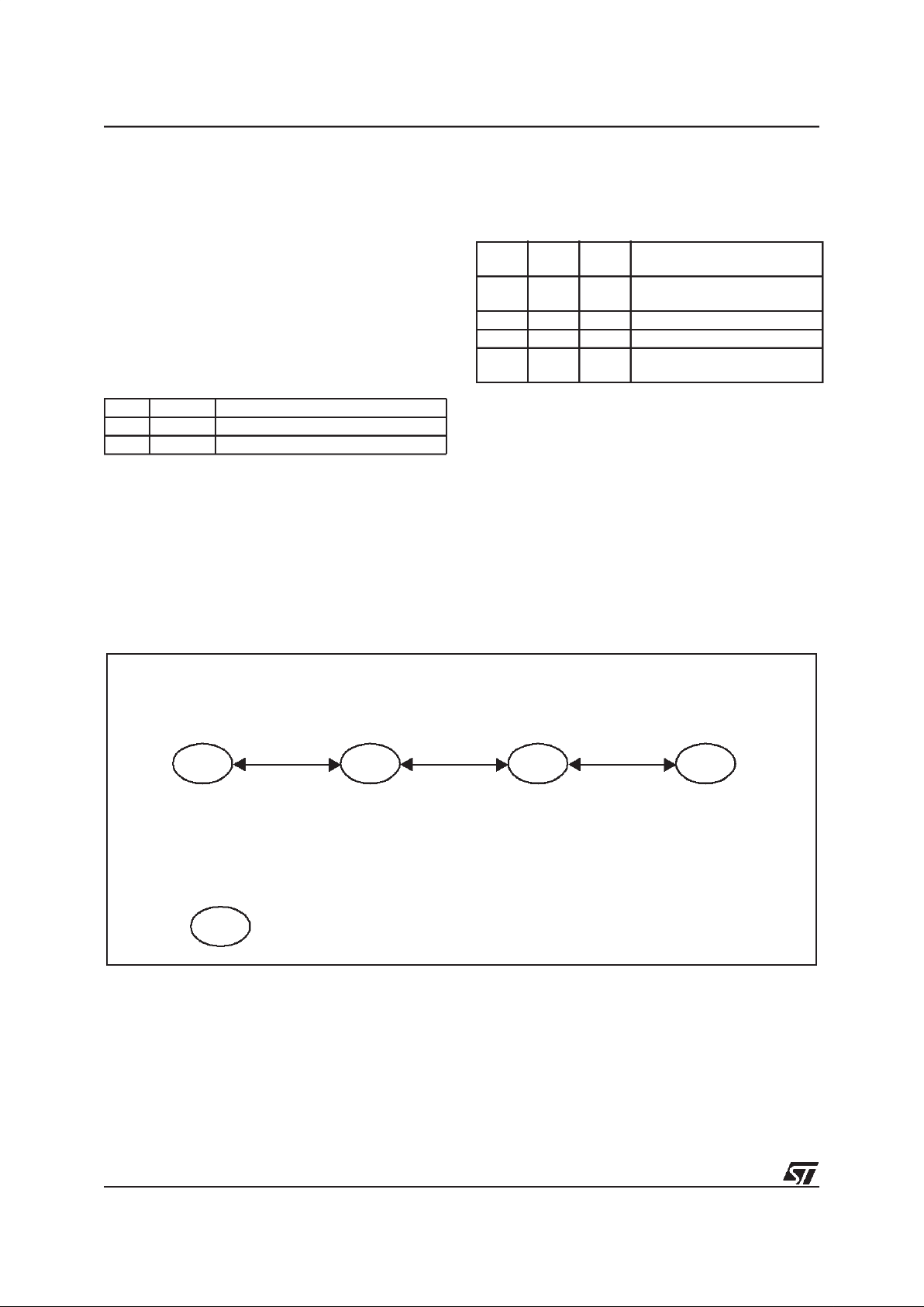
2 CENTRAL PROCESSING UNIT
2.1 INTRODUCTION
The CPU has a full 8-bit architecture. Six internal
registers allow efficient 8-bit data manipulation.
The CPU is capable of executing 63 basic instructions and features 17 main addressing modes.
2.2 CPU REGISTERS
The 6 CPU registers are shown in the programming model inFigure 2. Following an interrupt, all
registers except Y are pushed onto the stack in the
order shown in Figure 3. They are popped from
stack in the reverse order.
Accumulator (A). The Accumulator is an 8-bit
general purpose register used to hold operands
and the results of the arithmetic and logic calculations as well as data manipulations.
Index Registers (X and Y).These 8-bit registers
are used to create effective addresses or as temporary storage areas for data manipulation. The
Cross-Assembler generates a PRECEDE instruction (PRE) to indicate that the following instruction
refers to the Y register. The Y register is never automatically stacked. Interrupt routines must push
or pop it by using the PUSH and POP instructions.
Program Counter (PC).The program counter is a
16-bit register containing the address of the next
instruction to be executed by the CPU.
Figure 2. Organization of Internal CPU Registers
ACCUMULATOR:
X INDEX REGISTER:
Y INDEX REGISTER:
PROGRAM COUNTER:
STACKPOINTER:
CONDITION CODE REGISTER:
X = Undefined
RESET VALUE:
70
XXXXXXXX
RESET VALUE:
70
XXXXXXXX
RESET VALUE:
70
XXXXXXXX
15
70
RESET VALUE = DEVICE DEPENDENT,SEE MEMORY MAP
RESET VALUE:
70
XXXXXXXX
15
70
RESET VALUE = DEVICE DEPENDENT,SEE MEMORY MAP
14/117
ST7285C
CPU REGISTERS(Cont’d)
Stack Pointer (SP) The Stack Pointer is a 16-bit
register. Since the stack size can vary from device
to device, the appropriate number of most significant bits are forced so as to map the stack as defined in the Memory Map. The number of least significant digits thus available tothe user will depend
on the stack size, for example in the case of a 128
byte stack, 7 bits will be available whereas in the
case of a64 byte stack, only 6 bits will beavailable.
The stack is used to save the CPU context during
subroutine calls or interrupts. The user may also
directly manipulate the stack by means of the
PUSH and POP instructions.
Following an MCU Reset, or after a Restore following a Reset Stack Pointer instruction (RSP),
the StackPointer is set to point to thehighest location in the stack. It is then decremented after data
has been pushed onto the stack and incremented
after data is popped from the stack. When the lower limit is exceeded, the Stack Pointer wraps
around to the stack upper limit. The previously
stored information is then overwritten and therefore lost. The upper and lower limits of the stack
area are shown in the Memory Map.
A subroutine call occupies two locations and an interrupt five locations in the stack area.
Condition Code Register (CC) The Condition
Code register is a 5-bit register which indicates the
result of the instruction just executed as wellas the
state of the processor. These bits can be individually tested by a program and specified action taken
as a result of their state. The following paragraphs
describe each bit of the CC register in turn.
Half carry bit (H)The H bit is set to 1 when acarry
occurs between bits 3 and 4 of the ALU during an
ADD or ADC instruction. The H bit is useful in BCD
arithmetic subroutines.
Interrupt mask (I) When the I bit is set to 1, all interrupts except the TRAP software interrupt are
disabled. Clearing this bit enables interrupts to be
passed to the processor core. Interrupts requested
while I is set are latched and can be processed
when I is cleared (only one interrupt request per interrupt enable flag can be latched).
Negative (N)
When set to 1, this bit indicates that
the result of the last arithmetic, logical or data manipulation is negative (i.e. the most significant bit is
a logic 1).
Zero (Z)
When set to 1, this bit indicates that the
result of the last arithmetic, logical or data manipulation is zero.
Carry/Borrow (C) When set, C indicates that a
carry or borrow out of the ALU occured during the
last arithmetic operation. This bit is also affected
during execution of bit test, branch, shift, rotate
and store instructions.
Figure 3. Stacking Order
INCREASING
MEMORY
UNSTACK
ACCUMULATOR
X INDEX REGISTER
PCH
PCL
(PUSH)
DECREASING
MEMORY
111
VR000074
07
ADDRESSES
ADDRESSES
STACK
(POP)
CONDITION CODE
RETURN
INTERRUPT
15/117
ST7285C
3 CLOCKS, RESET, INTERRUPTS & POWER SAVING MODES
3.1 CLOCK SYSTEM
3.1.1 General Description
The MCU accepts either a Crystal or Ceramic resonator, or an external clock signal to drive the internal oscillator. The internal clock (CPU CLK running at f
CPU
) is derived from the external oscillator
frequency (f
OSC).
The external Oscillator clock is
first divided by 2, and an additional division factor
of 2, 4, 8, or 16 can be applied, in Slow Mode, to
reduce the frequency of the CPU clock (see
note 1); this clock signal is also routed to the onchip peripherals. The CPU clock signal consists of
a square wave with a duty cycle of 50%.
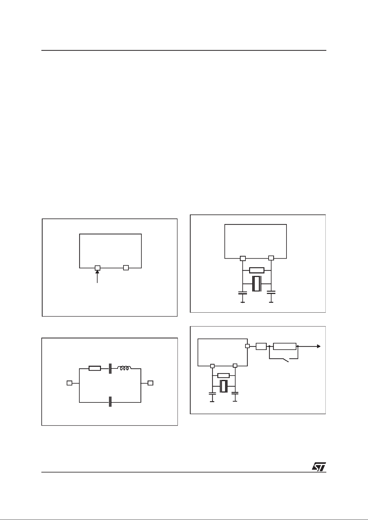
Figure 4. External Clock Source Connections
Figure 5. Equivalent Crystal Circuit
3.1.2 Crystal Resonator
The internal oscillator is designed to operate with
an AT-cut parallel resonant quartz crystal resonator in the frequency range specified for f
osc
.The
circuit shown in Figure 6 is recommended when
using a crystal, andTable 2 lists the recommended capacitance and feedback resistance values.
The crystal and associated components should be
mounted as close as possible to the input pins in
order to minimize output distortion and start-up
stabilisation time.
Use of an external CMOS oscillator is recommended when crystals outside the specified frequency ranges are to be used.
Figure 6. Crystal/Ceramic Resonator
Figure 7. Clock Prescaler Block Diagram
Note 1: Additional division factor of CPU clock is only available on L5/L6.
OSC
in
OSC
out
EXTERNAL
CLOCK
NC
OSC
in
OSC
out
R
S
L
1
C
1
C
0
OSC
in
OSC
out
C
OSCin
C
OSCout
R
P
OSC
in
OSC
out
C
OSCin
C
OSCout
R
P
%2 %2,4,8,16
CPUCLK
to CPU and
Peripherals
16/117
ST7285C
CLOCK SYSTEM (Cont’d)
3.1.3 Ceramic Resonator
A ceramic resonator may be used as an alternative to a crystal in low-cost applications. The circuit
shown in Figure 6 is recommended when using a
ceramic resonator. Table 3 lists the recommended
feedback capacitance and resistance values. The
manufacturer of the particular ceramic resonator
being considered should be consulted for specific
information.
Table 2. Recommended Values for Crystal
Resonator
3.1.4 External Clock
An external clock may be applied to the OSCin input with the OSCout pin not connected, as shown
on Figure 4. The t
OXOV
and t
ILCH
specifications do
not apply when using an external clock input. The
equivalent specification of the external clock
source should be used instead of t
OXOV
or t
ILCH
.
See CONTROL TIMING SECTION.
Table 3.Recommended Values for Ceramic
Resonator
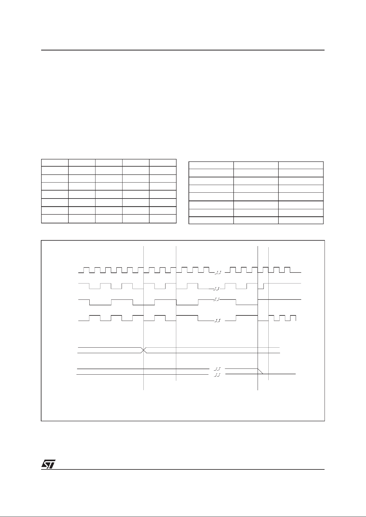
Figure 8. Timing Diagram for Internal CPU Clock Frequency transistions
2MHz 4MHz 8MHz Unit
R
SMAX
400 75 60 Ω
C
0
5 7 10 pF
C
1
81215fF
C
OSCin
15-40 15-30 15-25 pF
C
OSCout
15-30 15-25 15-20 pF
R
P
10 10 10 MΩ
Q304060
10
3
2-8MHz Unit
R
SMAX
10 Ω
C
0
40 pF
C
1
4.3 pF
C
OSCin
30 pF
C
OSCout
30 pF
R
P
1-10 MΩ
Q 1250
MISCELLANEOUS REGISTER
00 10
1
10
VR02062B
New frequency
requested
New frequency
active when
f
OSC
/4 & f
OSC
/8 = 0
Normalmode
active
Normalmode
requested
PSM1:PSM0
SMS
f
OSC
/2
f
OSC
/4
f
OSC
/8
f
CPU

17/117
ST7285C
3.2 MISCELLANEOUS REGISTER
The Miscellaneous register allows one to select
the SLOW operating mode and to set the clock division prescaler factor. Bits 3 and 4 allow one to
set PB7 functionality (I/O, CPU Clock o/p or Beep
signal o/p), while bits 6 and 7 determine the signal
conditions which will trigger an interrupt request on
I/O pins having interrupt capability.
Register Address: 0020h — Read/Write
Reset Value: 00h
b7, b6 -
EI1, EI0
:
External Interrupt Option
0 0 - Negative edge and low level (Reset state)
1 0 - Negative edge only
0 1 - Positive edge only
1 1 - Positive and negative edge
This selection applies globally to the four external
interrupts: I1, I2, I9 and I10.
b6 and b7 can be written only when the Interrupt
Mask (I) of the CC (Condition Code) register is set
to 1.
b5- Reserved
b4, b3 - SK1, CK0
:
Clock/Beep Output
0 0 - I/O port (Reset state)
1 0 - I/O port
0 1 - CPU Clock output to pin PB7
1 1 - 2KHz Beep signal output to pin PB7
(at 8.664 MHz oscillator frequency)
b2, b1 - SM1,SM0:
CPU clock prescaler for Slow
Mode
0 0 - Oscillator frequency / 4
1 0 - Oscillator frequency / 8
0 1 - Oscillator frequency / 16
1 1 - Oscillator frequency / 32
b0 - SMS:
Slow Mode Select
0- Normal mode - Oscillator frequency / 2
(Reset state)
1- Slow mode (Bits b1 and b2 define the prescaler
factor)
70
EI1 EI0 b5 SK1 CK0 SM1 SM0 SMS
18/117
ST7285C
3.3 RESETS
3.3.1 Introduction
There are four sources of Reset:
– RESET pin (external source)
– Power-On Reset (Internal source)
– WATCHDOG (Internal Source)
The Reset Service Routine vector is located at ad-
dress FFFEh-FFFFh.
3.3.2 External Reset
The RESET pin is both an input and an open-drain
output with integrated pull up resistor. When one
of the internal Reset sources is active, the Reset
pin is driven low to reset the whole application.
3.3.3 Reset Operation
The duration of the Reset condition, which is also
reflected on the output pin, is fixed at4096 internal
CPU Clock cycles. A Reset signal originating from
an external source must have a duration of at least
1.5 internal CPU Clock cycles in order to be recognised. At the end of the Power-On Reset cycle, the
MCU may be held in the Reset condition by an External Reset signal. The RESET pin may thus be
used to ensure VDDhas risen to a point where the
MCU can operate correctly before the User program is run. Following a Reset event, or after exit-
ing Halt mode, a 4096 CPU Clock cycle delay period is initiated in order to allow the oscillator to
stabilise and to ensure that recovery has taken
place from the Reset state.
During the Reset cycle, the device Reset pin acts
as an output that is pulsed low for 3 machine cycles (6 oscillator cycles). In its high state, an internal pull-up resistor of about 300KΩ is connected to
the Reset pin. This resistor can be pulled low by
external circuitry to reset the device.
3.3.4 Power-on Reset
This circuit detects the ramping up of VDD,and
generates a pulse thatis used to reset the application (at approximately VDD= 2V).
Power-On Reset is designed exclusively to cope
with power-up conditions, and should not be used
in order to attempt to detect a drop in the power
supply voltage.
Caution:
to re-initialize the Power-On Reset, the
power supply must fall below approximately 0.8V
(Vtn), prior to rising above 2V. If this condition is
not respected, on subsequent power-up the Reset
pulse may not be generated. An external pulse
may be required to correctly reactivate the circuit.
Figure 9. Reset Block Diagram
VDD
COUNTER
RESET
to ST7
VR2062C
300K
WATCHDOG RESET
OR DLPSS
RESET
OSCILLATOR
SIGNAL
INTERNAL
RESET
19/117
ST7285C
3.4 WATCHDOG TIMER SYSTEM (WDG)
3.4.1 Introduction
The Watchdog timer is used to detect the occurence of a software fault, usually generated by
external interference or by unforeseen logical conditions, which causes the application program to
abandon its normal sequence. The Watchdog circuit generates an MCU reset on expiry of a programmed time period, unless the program refreshes the counter’s contents before it is decremented
to zero.
3.4.2 Functional Description
The counter is decremented every 12,288 machine cycles, and the length of the timeout period
can be programmed by the user in 64 increments,
ranging from 12,288 machine cycles to 786,432
machine cycles, depending on the value loaded in
bits 0-5 of the Watchdog register. The application
program must be written so that the Watchdog
register is reloaded at regular intervals during normal operation.
The Watchdog is not activated automatically on
Reset, and must be activated by the user program
if required. Once activated it cannot be disabled,
save by a Reset.
During the Reset cycle, the device Reset pin acts
as an output that is pulsed low for 3 machine cycles (6 oscillator cycles). In its high state, an internal pull-up resistor of about 100KΩis connected to
the Reset pin.
This resistor can be pulled low by external circuitry
to reset the device.
The Watchdog delay time is defined by bits 5-0 of
the Watchdog register; bit 6 must always be set in
order to avoid generating an immediate reset.
Conversely, this can be used to generate a software reset (bit 7 = 1, bit 6 = 0).
Once bit 7 is set, it cannot be cleared by software:
i.e. the Watchdog cannot be disabled by software
without generating a Reset. The Watchdog timer
mustbe reloaded before bit 6 is decremented to ”0”
to avoid a Reset. Following a Reset, the Watchdog
register will contain 7Fh (bits 0-6 = 1, bit 7 = 0).
If the Watchdog is activated, the HALT instruction
will generate a Reset.
If the circuit is not used as a Watchdog (i.e. bit 7 is
never set), bits 6 to 0 may be used as a simple 7bit timer, for instance as a real time clock. Since no
interrupt will be generated under these conditions,
the Watchdog register must be monitored by software.
3.4.3 Watchdog Register
Register Address: 0024h — Read/Write
Reset Value: 0111 1111 (7Fh)
b7 = WDGA: Activation bit (is active if set)
b6-0 =
T6-T0
: 7-bit timer counter (Msb to Lsb)
Table 4. Watchdog Timing (f
OSC
= 8 MHz)
70
WDGA T6 T5 T4 T3 T2 T1 T0
WDG Register initial
value
WDG timeout period (ms)
FF 197
C0 3

20/117
ST7285C
3.5 INTERRUPTS
A list of interrupt sources is given inTable 5below,
together with relevant details for each source. Interrupts are serviced according to their order ofpriority, starting with I0, which has the highest priority, and so to I11, which has the lowest priority.
The following list describes the origins for each interrupt level:
– I0 connected to Software Interrupt (TRAP)
– I1 connected to Port G3
– I2 connected to Port F0, F1, F2, F3
– I3 connected to SPI A
– I4 connected to Timer A
– I5 connected to GBS interrupt
– I6 connected to Timer B
– I7 connected to SPI B
– I8 connected to SCI
– I9 connected to Ports D4, D5
– I10 connected to Ports C4, C5
– I11 connected to I2C
Exit from HALT mode may only be triggered by an
External Interrupt on one of the following ports:
C4(I10), C5(I10), D4(I9), D5(I9), F0(I2), F1(I2),
F2(I2), F3(I2) and G3(I1).
If more than one input pin of a group connected to
the same interrupt line is selected simultaneously,
these will be logically ORed.
Table 5. Interrupt Mapping
Interrupt
source
Vector
Address
Interrupts Register
Flag
name
CPU
interrupts
- FFFEh-FFFFh Reset N/A N/A RESET
I0 FFFCh-FFFDh Software N/A N/A TRAP
I1 FFFAh-FFFBh Ext. Interrupt (Port G3) N/A N/A INT1
I2 FFF8h-FFF9h Ex. Interrupt (Ports F0, F1, F2, F3) N/A N/A INT2
I3 FFF6h-FFF7h Transfer Complete SPI A Status SPIF1_A SPI_A
“ “ Mode Fault “ MODF1_A “
I4 FFF4h-FFF5h Input Capture 1 Timer A Status ICF1_A TIMER_A
“ “ Output Compare 1 “ OCF1_A “
“ “ Input Capture 2 “ ICF2_A “
“ “ Output Compare 2 “ OCF2_A “
“ “ Timer Overflow “ TOF_A “
I5 FFF2h-FFF3h RDS Block Interrupt. RDS GRP
VSI
CNI
GBS
I6 FFF0h-FFF1h Input Capture 1 Timer B Status ICF1_B TIMER_B
“ “ Output Compare 1 “ OCF1_B “
“ “ Input Capture 2 “ ICF2_B “
“ “ Output Compare 2 “ OCF2_B “
“ “ Timer Overflow “ TOF_B “
I7 FFEEh-FFEFh Transfer Complete SPI B Status SPIF2_B SPI_B
“ “ Mode Fault “ MODF1_B “
I8 FFECh-FFEDh Transmit Buffer Empty SCI Status TDRE SCI
“ “ Transmit Complete “ TC “
“ “ Receive Buffer Full “ RDRF “
“ “ Idle Line Detect “ IDLE “
“ “ Overrun “ OR “
I9 FFEAh-FFEBh Ext. Interrupt (Ports D4,D5) N/A N/A INT9
I10 FFE8h-FFE9h Ext. Interrupt (Port C4, C5) N/A N/A INT10
I11 FFE6h-FFE7h Byte Transmission Finished I
2
C Status BTF I2C
“ “ Bus Error “ BERR I2C
“ “ Stop Detection “ SSTOP I2C
21/117
ST7285C
INTERRUPTS (Cont’d)
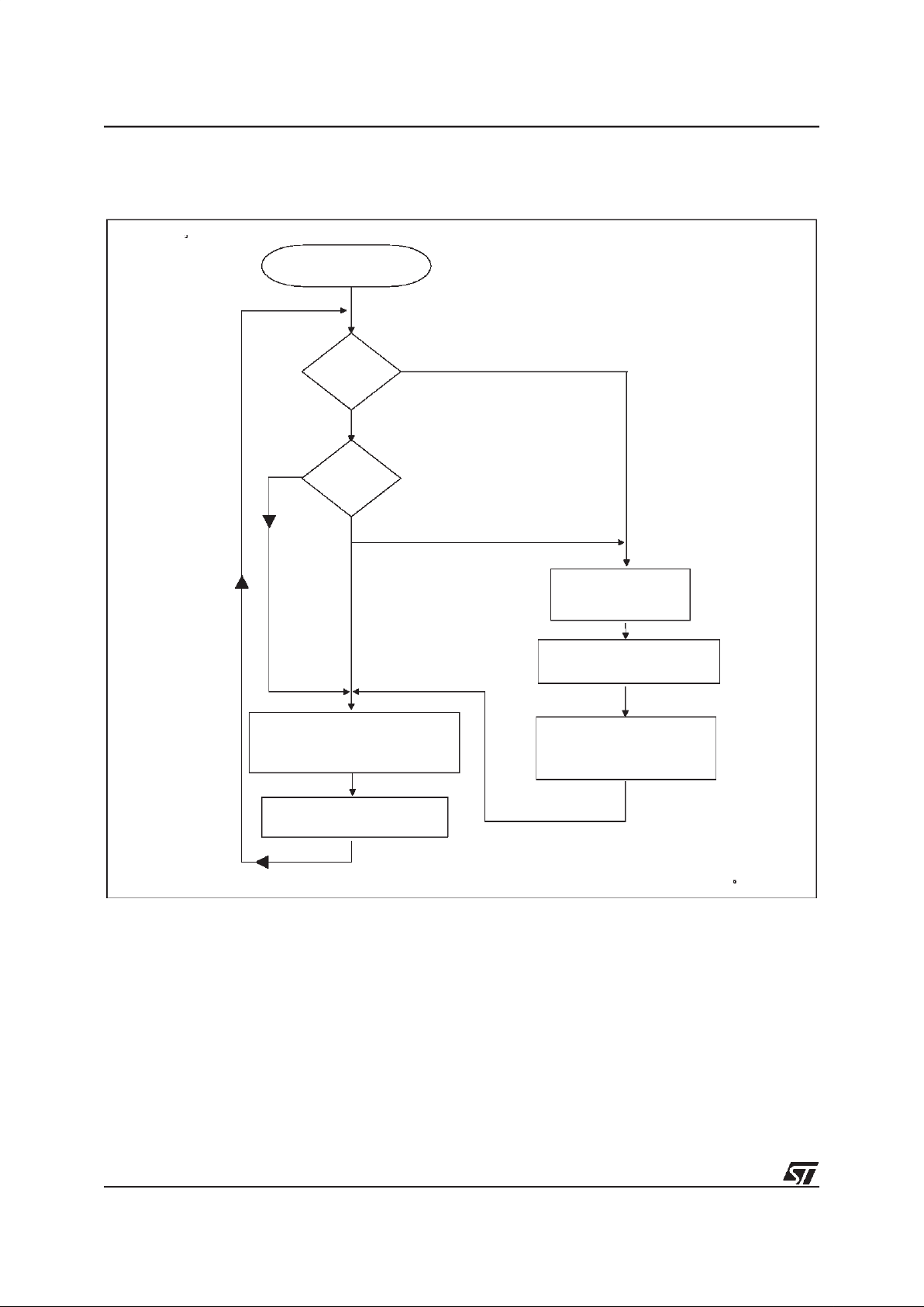
Figure 10. Interrupt Processing Flowchart
Note 1. See Table 5 . Interrupt Mapping
FROM RESET
TRAP
FETCH NEXT
INSTRUCTION
OF APPROPRIATE INTERRUPT
SERVICEROUTINE
EXECUTE INSTRUCTION
PUSH
PC,X,A,CC
SET I BIT TO 1
VR01172B
N
Y
LOAD PC
WITH APPROPRIATE
INTERRUPT VECTOR
(1)
I BIT = 1
N
Y
ONTO STACK
22/117
ST7285C
3.6 POWER SAVING MODES
3.6.1 Slow Mode
The following Power Saving mode may be selected by setting the relevant bits in the Miscellaneous
register as detailed in Section3.2.
In Slow Mode, the oscillator frequency can be divided by 4, 8, 16 or 32 rather than by 2. The CPU
and peripherals are clocked at this lower frequency, and therefore the RDS filter cannot operate
correctly in this mode. SLOW mode is used to reduce power consumption, and enables the user to
adapt clock frequency to available supply voltage.
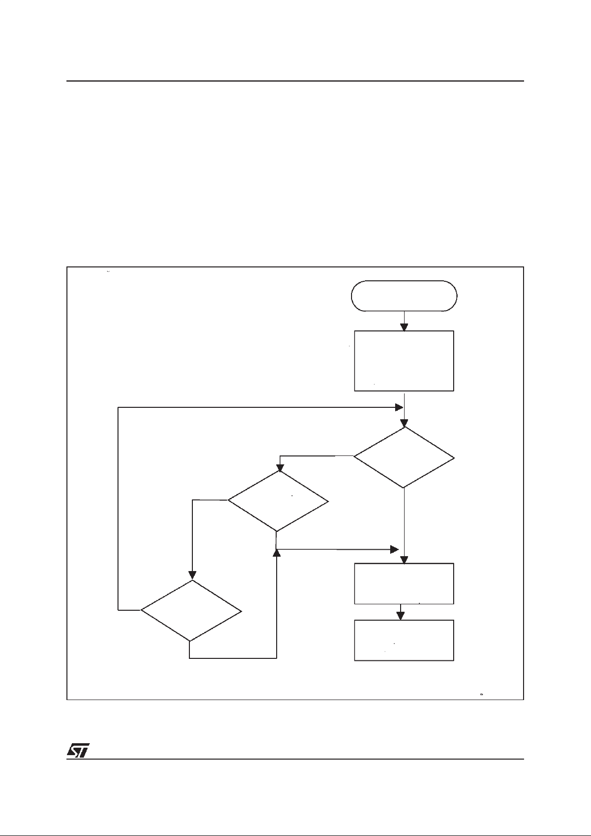
3.6.2 Wait Mode
WAIT mode places the MCU in a low power consumption mode by stopping the CPU. All peripherals remain active. During WAIT mode, the I bit (CC
Register) is cleared, so as to enable all interrupts.
All other registers and memory remain unchanged. The MCU will remain in WAIT mode until
an Interrupt or Reset occurs, whereupon the Program Counter branches to the starting address of
the Interrupt or Reset Service Routine.
Refer to Figure 11 below.
Figure 11. Wait Mode Flow Chart
WAIT
WAIT
Y
VR02062D
N
Y
Y
N
EXTERNAL
INTERRUPT
RESET
RESTART
PROCESSORCLOCK
FETCHRESET
VECTOROR
SERVICEINTERRUPT
PERIPHERAL
INTERRUPT
N
ACTIVE OSCILLATOR
AND PERIPHERALS
CLOCKSACTIVE
PROCESSORCLOCK
STOPPED
23/117
ST7285C
POWER SAVING MODES(Cont’d)
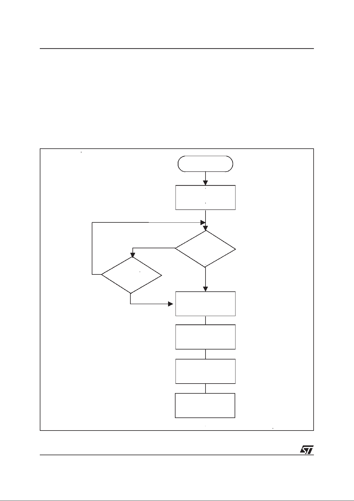
3.6.3 Halt Mode
The HALT instruction places the MCU in its lowest
power consumption mode. In HALT mode the internal oscillator is turned off, causing all internal
processing to be halted. During HALT mode, the I
bit in the CC Register is cleared so as to enable
External Interrupts.
All other registers and memory remain unaltered
and all Input/Output lines remain unchanged. This
state will endure until an External Interrupt (I1, I2,
I9, I10) or a Reset is generated, whereupon the internal oscillator is restarted. A delay of 4096 CPU
clock cycles is initiated prior to restarting the application, in order to allow the oscillator to stabilize.
The External Interrupt or Reset causes the Program Counter to be set to the address of the corresponding Interrupt or Reset Service Routine.
Figure 12. Halt Mode Flow Chart
N
Y
VR02062E
N
EXTERNAL
INTERRUPT
WAIT
HALT
Y
STOP OSCILLATOR
ANDALL CLOCKS
CLEARI-BIT
RESET
OSCILLATOR
IN SLOW MODE
TURN ON
OSCILLATOR
WAIT FOR 4096 CPU
CLOCK TIME DELAY
FETCH RESET
VECTOROR
SERVICEINTERRUPT

24/117
ST7285C
4 ON-CHIP PERIPHERALS
4.1 I/O PORTS
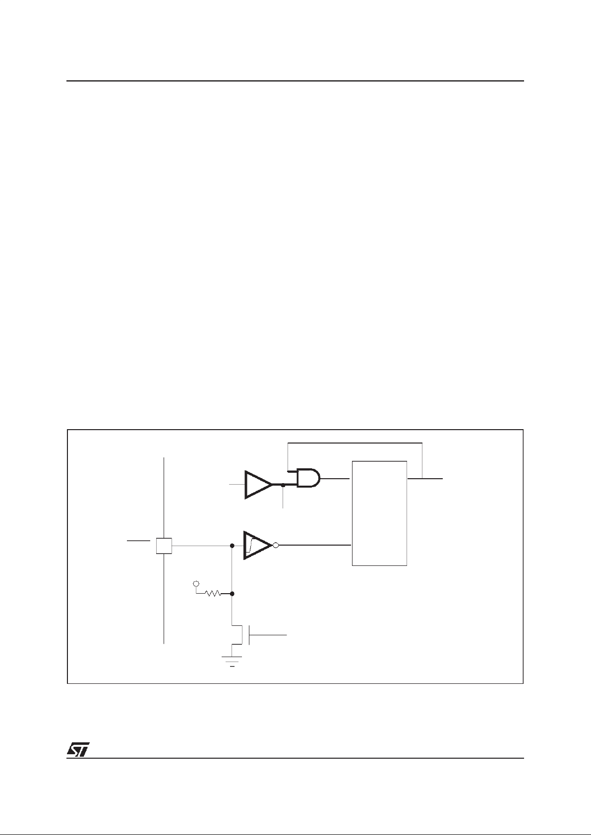
4.1.1 Introduction
Each I/O Port can contain up to 8 individually programmable I/Os. The MCU features seven 8-bit
Ports (A, B, C,... G) and one 6-bit-port (H). Each I/
O pin is dedicated to its main functionality, thus reducing and simplifying its programmability.
The current chapter describes the generic I/O
structure used in the MCU.
All I/Os are based on a generic circuit, of which a
block diagram is given inFigure 13. In most cases
the functions are simplified, and several subblocks may be missing (such as, for instance, the
analog switch on ports B to H or pull-up and interrupt logic for most of the I/O ports). Some registers
may also be absent where their functionality is redundant: it is therefore advisable to consult the
Memory Map in section1.3 and the pin description
in section 1.2 for proper use of any particular I/O.
Only ports C4, C5, D4, D5, F0,F1, F2, F3, G3 feature interrupt capability.
The following sub-section 4.1.2 contains generic
information on ST7 I/O ports. For information specific to this device, please refer to sub-section
4.1.3.
4.1.2 Generic I/O Features
The I/O ports offer the following generic features:
– inputs with Schmitt trigger
– analog inputs, when connected via internal mul-
tiplexer
– interrupt generation, maskable by software
– EMI compliance thanks to reduced noise radia-
tion due to lowered cross-current in push pull
mode and reduced input susceptibility. This fea-
ture is particularly relevant in RDS applications.
Each
generic
I/O pin may be individually program-
mable by software as:
– input: no pull-up, no interrupt generation
– input: pull-up, no interrupt generation
– input: pull-up, interrupt generation
– input: pull-down, no interrupt generation
– output: push-pull
– output: open-drain, no pull-up
– output: open-drain, with pull-up
4.1.2.1 Port Registers
Each port may be associated with up to four registers:
–
DATA REGISTER
(DR)
Address 0000 0000 000x xx00b; always present.
–
DATA DIRECTION REGISTER
(DDR)
Address 0000 0000 000x xx01b; always present.
–
OPTION REGISTER
(OR)
Address 0000 0000 000x xx10b; depending on
I/O dedication.
– PULL-UP REGISTER(PUR)
Address 0000 0000 000x xx11b; depending on
I/O dedication.
These are not internal CPU registers and must be
accessed by reading and writing to the relevant
memory locations. Refer toTable 1- Memory Map
for the respective addresses and reset values.
4.1.2.2 Functional Description
Each I/O pin may be programmed independently
as an analog input if the port features analog capabilities, as a digital input or a digital output with various variants, using the corresponding register
bits. When programmed as a digital input, a pull-up
or a pull-down resistor can, if present, be activated
by software. Only when enabling the pull-up, can
an interrupt function be programmed by software.
When programmed as an output, the I/O pin can
be programmed to operate either in push-pull or in
open-drain mode.
The interrupts generated by a port (active low) are
“ORed” to a single interrupt line that can be routed
to a CPU interrupt.
25/117
ST7285C
I/O PORTS (Cont’d)
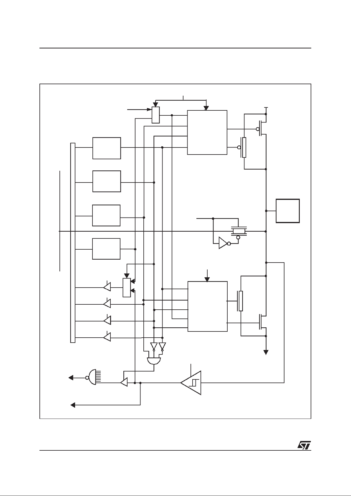
Figure 13. Generic I/O Circuitry
V
DD
PAD
FROM
OTHER
BITS
DR SEL
OR SEL
DDR SEL
PUR SEL
PUR
DDR
OR
DR
DAT A BUS
INTERRUPT
M
U
X
SIGNAL FROM ALTERNATE
TRIGGER ENABLE
PAD_TRIG
ANALOG
SWITCH
ANALOG ENABLE
COMMON ANALOG RAIL
from
ADC
M
U
X
ALTERNATE FUNCTION ENABLE
CONFIGURATION
DECODER
ALTERNATE FUNCTION ENABLE
CONFIGURATION
DECODER
FUNCTION
26/117
ST7285C
I/O PORTS (Cont’d)
4.1.2.3 Operating Modes
All I/O pins may be configured as inputs or outputs
by programming the corresponding bits of the DR,
DDR, OR and PUR memory-mapped registers.
Table 6 illustrates the available operating modes.
During Reset, DR, DDR, OR and PUR are initialized to a Low level.
Table 6. I/O Operating Modes
Note:
(1) This state can add static current consumption.
– Input Mode
In input mode, both the analog multiplexer and the
port buffer are switchedto a high impedance state.
To avoid ringing with slowly rising or falling input
signals and to increase noise immunity, the inputs
are equipped with Schmitt-triggers.
The state of the pin is readable through the Data
Register. The pin state is read directly from the
Schmitt Trigger’s output and not from the Data
Register.
There are four different input modes, as illustrated
in Table 6.
Note: Pull-up and pull-down devices are not implemented by means of linear resistors, but by means
of resistive transistors.
– Interrupt function
The interrupt signals of all activated bits are
NANDed together, so that whenever at least one
of the activated inputs goes low, the port’s common interrupt output will go high in order to activate the CPU interrupt input.
– Output Mode
In output mode, the port output buffer is activated
and drives the output according to the content of
the data register, DR. In this mode, the analog
multiplexer, when present, is switched to high impedance and the interrupt is disabled.
Data written to the DR is directly copied to the output pins. A read operation of DR will be directly
performed from the DR register, so that the output
data stored in DR is readable, regardless of the
logic levels at the output pin due to output loading.
There are three different output modes for the
standard I/O pins as illustrated inTable 6.
– Alternate function
Alternate functions take priority over standard I/O
programming; if a peripheral needs to use a pad,
the alternate function is automatically activated.
The signal from the peripheral is output to the pad
(automatically configured in this case in push-pull
or open drain modes without pull-up and pulldown), and controlled directly by the peripheral.
The signal to be input to the peripheral from the
pad is taken after the schmitt trigger and is controlled directly by the peripheral. In this case, the pin’s
state is readable as in Input Mode by addressing
the Data Register and by configuring the PAD in
Input Mode (DDR=0).
– Analog Input Mode
In analog input mode (activated by the ADC), the
analog multiplexer is activated and switches the
analog voltage present on the selected pin (pins
PA0 to PA7) to the common analog rail. The common analog rail is connected to the Analog to Digital converter (see Section4.6) input. It is not recommended to change the voltage level or loading
on any port pin while conversion is in progress.
Furthermore it is not recommended to have clocking pins located close to a selected analog pad.
WARNING: Before activating the Analog Input
Mode, the I/O state must be set to:
INPUT, NO PULL-UP, NO INTERRUPT
(DDR = 0, OR = 0, PUR = 1)
The alternate function must not be activated as
long as the pad is configured as Input with Interrupt, in order to avoid generating spurious interrupts.
Analog input mode is only implemented for pins
PA0 to PA7. The analog input voltage level must
be within the limits stated in the Absolute Maximum Ratings.
DDR OR PUR Mode Option
0 0 0 input pull-up, no interrupt
0 0 1 input no pull-up, no interrupt
0 1 0 input pull-up, interrupt
0 1 1 input pull-down, no interrupt
1 0 0 output open-drain, pull-up
1 0 1 output open-drain, no pull-up
1 1 0 output RESERVED
(1)
1 1 1 output
push-pull, nopull-up, no
pull-down
27/117
ST7285C
I/O PORTS (Cont’d)
4.1.3 I/O Port Implementation
On the ST7285C, the pull down is always absent,
the pull up exists only where an interrupt facility is
present (Ports C4, C5, D4, D5, F0, F1, F2, F3,
G3). On port A, the analog inputs are directly controlled by the ADC.The I/O port register configurations are reduced to the following.
4.1.3.1 Ports A0-A7, B0-B7, C0-C3, C6, C7, D0D3, D6, D7,E0-E7, F4-F7, G0-G2, G4-G7, H0-H5
These ports do not offer interrupt capabilities.
Note: Open drain I/O is implemented on I2C pins
(pins 19 and 20) and high voltage pins (PH3/4/5).
The design uses special I/O devices without P
channel, thus forbidding the push pull configuration.
In this case there is neither pull up register nor option register. These registers do not exist and so
cannot be read or written to.
4.1.3.2 Ports C4, C5, D4, D5, F0-F3, G3
These ports offer interrupt capabilities.
In this case there is no pull up register since the
pull-up is present only when the interrupt feature is
selected. This register does not exist and so cannot be read or written to.
Switching these I/O ports from one state to another should be done in such a sequence as to prevent unwanted side effects. Recommended safe
transitions are illustrated inFigure 14. Other transitions are potentially risky and should be avoided,
since they are likely to present unwanted side-effects such as spurious interrupt generation.
Figure 14. Recommended I/O State Transition Diagram
DDR MODE OPTION
0 input no pull-up, no pull-down, no interrupt
1 output push-pull (or open drain: see note)
DDR OR
MOD
E
OPTION
0 0 input
no pull-up, no pull-down,
no interrupt
0 1 input interrupt, pull-up
1 0 output open-drain, no pull-up
1 1 output
push-pull, no pull-up,
no pull-down
110001
Interrupt
pull-up
push-pull
no pull-up
open-drain
no pull-up
no pull-down
INPUT
OUTPUT
OUTPUT
10
no pull-up
no interrupt
INPUT
no pull-down
(Reset state)
XX
= DDR, OR

28/117
ST7285C
4.2 SERIAL COMMUNICATIONS INTERFACE
4.2.1 Introduction
The Serial Communications Interface (SCI) offers
a flexible means of full-duplex data exchange with
external equipment requiring an industry standard
NRZ asynchronous serial data format. The SCI offers a very wide range of Baud rates thanks to the
presence of two Baud rate generator systems: the
first is of conventional type and yields common
communications Baud rates with standard oscillator frequencies; the second features a programmable prescaler capable of dividing the input frequency by any factor from 1 to 255, thus offering a
very wide range of Baud rates even with nonstandard oscillator frequencies. Transmitter and
Receiver circuits are independent and can operate
at different Baud rates; indeed, each can select either type of Baud rate generator. External connections are by means of two I/O pins: TDO (Port
PB0) for the Transmit Data output and RDI (Port
PB1) for the Receive Data input.
4.2.2 Features
– Full duplex, asynchronous communications
– NRZ standard format (Mark/Space)
– Dual Baud rate generator systems
– Independently programmable transmission and
reception Baud rates
– Separate Transmit and Receive Baud rates
– Programmable word length (8 or 9 bits)
– Receive buffer full, Transmit buffer empty and
End of Transmission flags
– Receiver wake-up function by the most signifi-
cant bit or by idle line
– Muting function for multiprocessor configurations
–Separate enable bitsforTransmitter andReceiver
– Noise, Overrun and Frame Error detection
– Four interrupt sources with flags
– Overall accuracy better than 1% of Baud rate.
4.2.3 Serial Data Format
Serial data is transmitted and received as frames
comprising the following elements:
– An Idle Line in the ”high” state prior to transmis-
sion or reception.
– A Start bit inthe ”low” state, denoting the start of
each character.
– Character dataword (8 or 9 bits), least significant
bit first.
– A Stop bit in the ”high” state, indicating that the
frame is complete.
Word length may be selected as being either 8 or 9
bits by programming the M bit in the SCCR1 control register.
An Idle Line condition is interpreted on receiving
an entire frame of ”ones”.
A Break is interpreted on receiving ”zeros” for
some multiple of the frame period.
4.2.4 Data Reception and Transmission
The following description is best read with reference to the SCI Block Diagram illustrated in Figure
1, where it will be noted that the SCDR data register is shown as two separate registers, one for
transmitted data and the other for received data.
The Serial Communications Data Register (SCDR)
performs a dual function (Read And Write),since it
accesses two separate registers, one for transmission (TDR) and one for reception (RDR). The TDR
register provides the data interface between the internal bus and the output shiftregister for data to be
transmitted, while the RDR register provides an interface between the input shift register and the internal bus for incoming data.
When the SCDR is read, the RDR is accessed and
its contents are transferred to the data bus. The
RDRF (RDR Full Flag) in the SCSR register is set
to ”1” as soon as the word in the receiver shift register is transferred to the RDR register.
When the SCDR is written to, the data word is
transferred to the TDR register. The TDRE flag
(TDR empty) in the SCSR register is set to ”1” as
soon as the word in the TDR is transferred to the
transmit shift register.
Incoming data is received in a serial shift register
and then transferred to a parallel Receive Data
Register (RDR) as a complete word, thus allowing
the next incoming character to be received in the
shift register while the current character is still in
the RDR.
Oversampling techniques are used for data recovery by discriminating between valid incoming data
and noise.
4.2.5 Receiver Muting and Wake-up Feature
In multiprocessor configurations it is often desirable that only the intended message recipient
should actively receive the full message contents,
thus reducing redundant SCI service overheads
for all non addressed receivers. Communications
protocols in such configurations generally issue
the recipient address as a message header.

29/117
ST7285C
SERIAL COMMUNICATIONS INTERFACE(Cont’d)
Each receiving device decodes this address header under program control and all non addressed
receivers may be placed in a sleep mode by
means of the Muting function, thus avoiding the
message contents from generating unnecessary
requests for service. This is achieved by inhibiting
all reception flags and interrupt generation when
Muting is enabled. A muted receiver may be reawakened in one of two ways: by Idle Line detection or by Address Mark detection. The wake-up
method may be programmed by programming the
WAKE bit in the SCCR1 register.
Receiver wake-up by Idle Line detection takes
place as soon as the Receive line is recognised as
being idle. An Idle Line condition is detected upon
receiving 10 or 11 consecutive ”ones”, depending
on whether a word has been defined as comprising 8 or 9 data bits. This wake-up method is selected by programming the WAKE bit to ”0”.
Receiver wake-up by Address Mark detection
takes place on receiving a ”1” as the most significant bit of a word, thus indicating that the message
is an address. This wake-up method is selected by
programming the WAKE bit to ”1”.
4.2.6 Baud Rate Generation
The following description is best read with reference to the SCI Baud Rate and External Prescaler
Diagram illustrated in Figure 2.
The CPU Clock is first divided by 16 by the first divisor block, then again divided by the division factor selected for the first prescaler, indicated by PR.
This division factor can be selected to be 1, 3, 4 or
13, depending on the setting of the SCP0 and
SCP1 bits (bits 6 and 7) in the SCBRR register (refer to the register description). The output from the
first prescaler will thus be the CPU Clock frequency divided by 16, 48, 64 or 208. This master clock
is available both to the conventional Baud Rate
Generator and to the External Prescaler.
The conventional Baud Rate Generator is enabled
by setting the relevant section (RX or TX) of the
External Prescaler to 00h. In this case the master
clock frequency is further divided by 1, 2, 4, 8, 16,
32, 64 or 128, depending on the settings of bits
SCT0, SCT1 and SCT2 in the case of the transmitter, and SCR0, SCR1 and SCR2 in the case of the
receiver (refer to the SCBRR register description).
If the External Prescaler Receive or Transmit
Baud Rate Register, PSBRT or PSBRR is set to a
value other than zero, that section of the prescaler
will be operational in place of the conventional
Baud Rate Generator. The output clock rate sent
to the transmitter or to the receiver will be the output from the first prescaler divided by a factor
ranging from 1 to 255 set in the External Prescaler
Receive or Transmit Baud Rate Register. As can
be seen the External Prescaler option gives a very
fine degree of control on the Baud rate, whereas
the conventional Baud Rate Generator retains industry standard software compatibility.
4.2.7 SCI Register Overview
The registers described in the following paragraphs allow full control of the various features
and parameters of the Serial Communications Interface. Refer also to the Memory Map.
4.2.7.1 Data Register (SCDR)
Address: 0051h — Read/Write
Reset Value: XXh
Contains the Received or Transmitted data char-
acter, depending on whether it is read or written to.
4.2.7.2 Control Register 1 (SCCR1)
Address: 0053h — Read/Write
Reset Value: XXh
Contains bits to select the desired word length and
the wake-up mode.
Bit-7 = R8
Receive Data Bit 8
If bit M is set at one, R8 will be used to store the
9th bit on reception.
Bit-6 = T8
Transmit Data Bit 8
Used to store the 9th data bit of the transmitted
word, when 9-bit word length is selected (bit M set
to ”1”).
Bit-4 = M
Word Length
Determines the word length:
0 = 1 Start bit, 8 Data bits, 1 Stop bit
1 = 1 Start bit, 9 Data bits, 1 Stop bit
Bit-3 = WAKE
Wake-Up Method
1 = Address Mark
0 = Idle Line
76543210
R8 T8 - M WAKE - - -

30/117
ST7285C
SERIAL COMMUNICATIONS INTERFACE(Cont’d)
4.2.7.3 Control Register 2 (SCCR2)
Address: 0054h — Read/Write
Reset Value: 00h
Contains four control bits which allow interrupts
generated by TDR Empty, Transmit Complete,
RDR Full and Idle Line to be enabled or disabled.
Also contains four control bits to enable or disable
Transmission, Reception, Receiver Wake-Up and
Send Break.
Bit-7 =
TIE
Transmitter Interrupt Enable
Authorizes an interrupt when set at one and when
the TDRE (transmission register empty) flag is set
to “1” indicating that the last word has been transmitted. When TIE is at zero this interrupt is disabled.
Bit-6 = TCIE
Transmission Complete Interrupt En-
able
This bit setto “1” enables an interrupt when theTC
flag (transmission competed) changes to “1”.
When TCIE is at “0” this interrupt is disabled.
Bit-5 = RIE
Receiver Interrupt Enable
Authorizes an interrupt when set to “1” and when
either the RDRF (Receive Data Register Full) flag
or the OR (Overspeed on Reception) flag is set to
“1”, indicating that the last word has been transmitted. When TIE is set to “0”, this interrupt is disabled.
Bit-4 = ILIE
Idle Line Interrupt Enable
This bit at “1” enables an interrupt if the IDLE flag
changes to “1” (which corresponds to an idle line
on reception). The interrupt cannot occur if the
IDLE bit is at “0”.
Bit-3 =
TE
Transmitter Enable
This bit at “1” enables the transmitter. At start-up,
the transmitter sends a preamble (ten or eleven
ones). During transmission, a “0” pulse on the TE
bit (“0” followed by “1”) sends a preamble after the
current word. Setting the TE bit to “0” switches the
output line to a high impedance state at the end of
the word currently being transmitted.
Bit-2 = RE
Receiver Enable
The RE bit at “1” enables the receiver which begins searching for a START bit. The RE bit at “0”
disables the receiver and resets the associated
status bits to “0” (RDRF, IDLE, OR, NF and FE).
Bit-1 = RWU
Receiver Wake-Up
The RWU bit at “1” mutes the receiver. The wakeup mode is determined by the WAKE bit (bit 3 in
SCCR1). As long as RWU remains at “1”, the flags
relating to the receiver cannot rise to “1”.
Writing “0” to RWU forces an exit from the muted
state.
As soon as the wake-up sequence is recognized,
the RWU bit is forced to “0”. If the wake-up selected mode corresponds to the reception of a preamble, the RWU bit cannot be set to “1” as long as the
reception remains idle. If the selected wake-up
mode corresponds to the reception of a “1” on the
most significant bit, the reception of this particular
word wakes up the receiver and sets the RDRF
flag to “1”, which allows the receiver to receive this
word normally and to use it as an address word.
Bit-0 = SBK
Send Break
This bit set to “1” tells the transmitter to send a
whole number of BREAKS (all bits at “0” including
the stop bit). At the end of the last BREAK the
transmitter inserts an extra “1” bit in order to acknowledge the START bit. If the SBK bit is set to
“1” and then to “0”, the transmitter will send a
BREAK word at the end of the current word.
4.2.7.4 Status Register (SCSR)
Address: 0050h — Read Only
Reset Value: 1100 0000b
Contains four flags which denote conditions which
can lead to interrupts if the corresponding bits of
SCCR2 are set: TDR Empty, Transmit Complete,
RDR Full and Idle Line. These flags are used for
management of the SCI interrupt system.
Also contains three flags which indicate error conditions due to Overrun, Noise and Framing.
Bit-7 =TDRE
Transmit Data Register Empty
Indicates that the content of the transmission data
register has been transferred into the shift register.
If the TDRE bit is at “0”, it indicates that the transmission has not yet occurred and that a write operation into the data register would overwrite previous data. The TDRE bit is reset to “0” by an SCSR
access followed by a write operation into the transmission data register. Data will not be transferred
to the shift register as long as the TDRE bit is not
reset to “0”.
Bit-6 =
TC
Transmission Complete
76543210
TIE TCIE RIE ILIE TE RE RWU SBK
76543210
TDRE TC RDRF IDLE OR NF FE -
 Loading...