

SANYO LA1137NM, LA1137N, LA1136NM, LA1136N Datasheet

Ordering number: EN 3507
Monolithic Linear IC
LA1136N, 1136NM, 1137N, 1137NM
AM Tuners for Car Radios and Home Stereos
Overview
The LA1136N/NM and LA1137N/NM are high-performance
AM electronic tuner ICs offering sophisticated functions. They
are especially suited for use in car radio and home stereo
(antenna: loop) applications.
Functions
.
MIX
.
OSC (with ALC)
.
IF amplifier
.
Detector
.
AGC (normal)
.
RF wide-band AGC
.
Auto search stop signal (Signal meter output)
.
Local oscillation buffer output
.
IF band switching circuit (for LA1136N only)
.
IF count buffer
.
Stop detector output (can be set independently)
.
Tweet prevention circuit
.
AGC (RF, IF) time constant switching circuit
.
IF AGC circuit
.
Pin-diode driver
.
AM stereo decoder IF output (for LA1136N only)
.
Circuit preventing incorrect seek operation
Features
.
Excellent cross modulation characteristic: Meets the
requirements for preventing not only adjacent-channel
interference but also interference caused by all channels
within broadcast band.
.
Narrow-band signal meter output: Usable as auto search stop
signal. Has linearity up to 100 dBµ.
.
Local oscillation buffer output: Facilitates designing of
electronic tuner system, frequency display, etc.
.
OSC (with ALC): Improves tracking error because
oscillation output is stabilized at a low level (350 mVrms:
LA1137N) for varactor diode.
.
MIX: Double-balanced differential MIX meeting the
requirements for preventing spurious interference, IF
interference.
.
Good characteristic at high input: 130 dBµ input
fm = 400 Hz 80%mod THD = 0.5% typ.
.
High S/N: Good S/N at medium input (55 dB typ).
.
Usable sensitivity: (S/N = 20 dB input): 25 dBµ
(when using 2SK715 )
.
VCCvariation compensation: Less variation in gain,
distortion: 8 to 12 V
AM stereo capability (LA1136N only)
.
IF band switching circuit on chip; controlled by
microcontroller
.
Oscillating circuit for AM stereo; SUB S/N improved to
6dB
.
IF output for AM stereo decoder
.
Improved tweet characteristics: 10 dB increase, controlled by
microcontroller
.
Improved cross modulation characteristics, especially
sensitivity suppression characteristics: 15 dB improvement,
wide-band AGC operation even for SW band interference
.
Improved low-frequency modulation distortion
.
Improved temperature characteristics: S-meter, SD sensitivity
.
Faster RF AGC response: RF: 1/3; IF: 1/8 (compared to
predecessors)
.
Improved capability for driving external RF AGC transistors:
I
max = 200 µA
B
.
Measures to prevent incorrect seek operation
.
IF count buffer on chip; controlled by microcontroller
.
Time constant switching circuit on chip for RF and IF
AGC
.
IF AGC clear circuit on chip
.
Measures that prevent stopping one station too soon
SANYO Electric Co.,Ltd. Semiconductor Bussiness Headquarters
TOKYO OFFICE Tokyo Bldg., 1-10, 1 Chome, Ueno, Taito-ku, TOKYO, 110 JAPAN
93097HA(II)/4281TS(US) No.3507-1/28
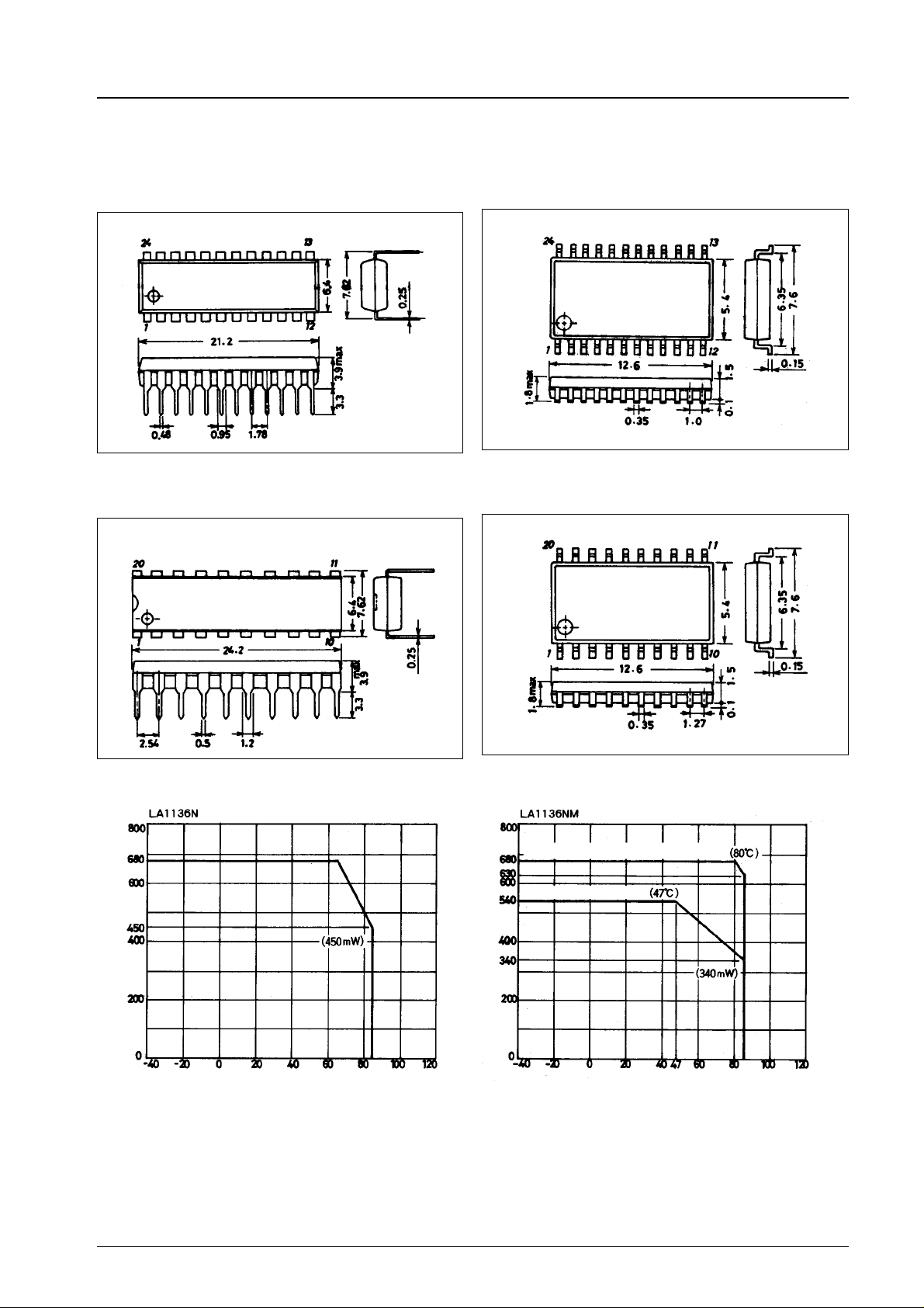
Package Dimensions
unit : mm
3067-DIP24S
LA1136N, 1136NM, 1137N, 1137NM
unit : mm
3112-MFP24S
unit : mm
3021B-DIP20S
[LA1136N]
[LA1137N]
SANYO : DIP24S
[LA1136NM]
SANYO : MFP24S
unit : mm
3036B-MFP20
[LA1137NM]
SANYO : DIP20Slim
Pdmax–Ta Pdmax–Ta
Mounted on 20 × 40 × 1.5 mm PCB
Independent IC
Allowable power dissipation, Pd max – mW
Ambient temperature, Ta – °C
Allowable power dissipation, Pd max – mW
Ambient temperature, Ta – °C
SANYO : MFP20
No. 3507-2/28
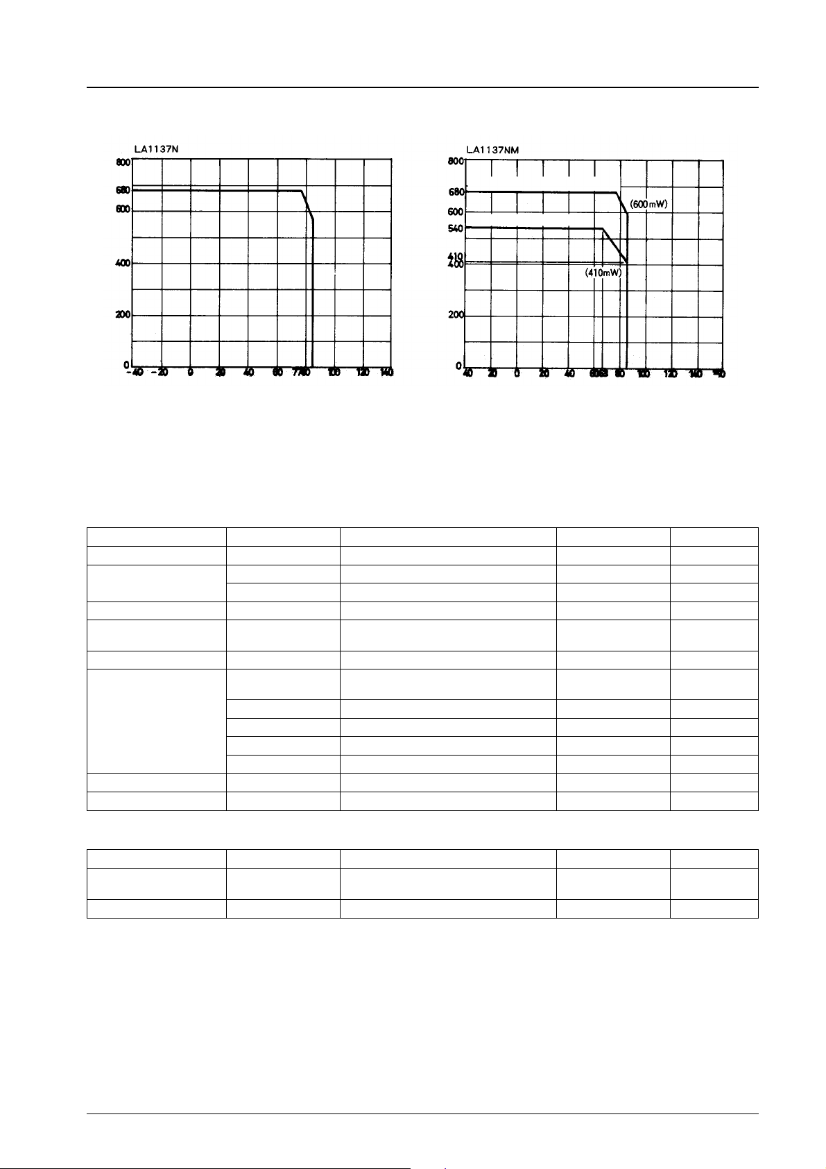
LA1136N, 1136NM, 1137N, 1137NM
Pdmax–Ta Pdmax–Ta
Mounted on 20 × 40 × 1.5 mm PCB
Independent IC
Allowable power dissipation, Pd max – mW
Ambient temperature, Ta – °C
Allowable power dissipation, Pd max – mW
Ambient temperature, Ta – °C
Specifications
Maximum Ratings at Ta = 25°C
Parameter Symbol Conditions Ratings Unit
Maximum supply voltage V
Output voltage V
Input voltage V
Current drain I
Flow-out current I
Allowable power
dissipation
Operating temperature Topr –40 to +85 °C
Storage temperature Tstg –40 to +125 °C
max Pin 19 (LA1136N), Pin 15 (LA1137N) 12 V
CC
1 Pin 6 13.4 V
O
V
2 Pin 13 (LA1136N), Pin 10 (LA1137N) 15.5 V
O
IN
CC
20
Pd max Ta % 65°C (LA1136N),
Pd max1 Independent IC, Ta % 47°C (LA1136NM) 540 mW
Pd max2 With PCB, Ta % 80°C (LA1136NM) 680 mW
Pd max1 Independent IC, Ta % 63°C (LA1137NM) 540 mW
Pd max2 With PCB, Ta % 77°C (LA1137NM) 680 mW
Pin 5 5.6 V
Pin 15+6+10, V11= 0 (LA1137N)
Pin 6+13+19, V
Pin 20 (LA1137N), Pin 24 (LA1136N) 2 mA
Ta % 77°C (LA1137N)
= 0 (LA1136N)
14
60 mA
680 mW
Operating Conditions at Ta = 25°C
Parameter Symbol Conditions Ratings Unit
Recommended supply
voltage
Supply voltage range V
V
CC
op 7.5to 10 V
CC
8V
No. 3507-3/28
LA1136N, 1136NM, 1137N, 1137NM
LA1136N, LA1136NM
Operating Conditions at Ta = 25°C, VCC= 8 V, fr = 1 MHz, fm = 400 Hz, See specified Test Circuit
Parameter Symbol Conditions
Current drain
I
I
Detection output V
1 Quiescent L L L O 22 38 52
CC
2 130 dBµ L L L O 30 45 60
CC
74 dBµ, 30% modulation L L L O –15.0 –12.0 –9.0 dBm
O
Pin
12 14 17 22
min typ max Unit
Signal-to-noise ratio S/N 74 dBµ, 30% modulation L L L O 49 54 dB
74 dBµ, 30% modulation,
AGC figure-of-merit AGC
reference output 10 dB below
LLLO 50 54 dBµ
input
Total harmonic distortion
Signal meter output voltage
Stop detector sensitivity SD V
Local-oscillator buffer output
voltage
IF buffer output voltage V
IF count buffer output voltage V
IF count buffer output leakage
voltage
Antenna input level for RF AGC
ON and tweet prevention
Antenna input for wideband AGC
ON
Wideband/narrowband detector
output ratio (weak input)
Pin-diode driver current I
THD1 74 dBµ, 80% modulation L L L O 0.4 1.0
THD2 130 dBµ, 80% modulation L L L O 0.5 2.0
V
1 Quiescent L L L O 0 0.3
SM
V
2 130 dBµ L L L O 3.5 5.0 7.5
SM
V
OSC
BUFF
BUFF 74 dBµ, zero modulation L L L O 530 750 1,000 mVrms
IF
IFCB
V
IFCBL
= 3.5 V L H L O 26 32 38 dBµ
18
Quiescent L L L O 270 330 mVrms
30 dBµ, zero modulation L H H O 260 300 mVrms
74 dBµ, zero modulation L L L O 10 mVrms
ANT1 LLLL 56 62 68dBµ
Quiescent, 1.0 MHz receive
ANT2
signal, 1.4 MHz interference,
L L L O 92 98 104 dBµ
zero modulation
– 21 dBµ, 30% modulation L/H L L O 2 4 dB
ANTDV1
= 0.7 V L L L O 4.0 5.5 mA
Note) SW voltage:H=5V,L=GND, O = OPEN
mA
%
V
LA1137N, LA1137NM
Operating Characteristics at Ta = 25°C, VCC= 8 V, fr = 1 MHz, fm = 400 Hz, See specified Test Circuit
Parameter Symbol Conditions
I
1 Quiescent L L O 22 38 52
Current drain
Detection output V
CC
I
2 130 dBµ, zero modulation L L O 30 45 60
CC
74 dBµ, 30% modulation L L O –15.0 –12.0 –9.0 dBm
O
Signal-to-noise ratio S/N 74 dBµ, 30% modulation L L O 50 55 dB
74 dBµ, 30% modulation,
AGC figure-of-merit AGC
reference output 10 dB below
input
Total harmonic distortion
Signal meter output
voltage
Stop detector sensitivity SD V
Local-oscillator buffer
output voltage
IF count buffer output
voltage
IF count buffer output
leakage voltage
THD1 74 dBµ, 80% modulation L L O 0.3 1.0
THD2 130 dBµ, 80% modulation L L O 0.4 2.0
V
1 Quiescent L L O 0 0.3
SM
V
2 130 dBµ, zero modulation L L O 3.5 5 7.5
SM
V
BUFF Quiescent L L O 290 350 mVrms
OSC
V
IFCB
V
IFCBL
= 3.5 V, zero modulation H L O 27 33 39 dBµ
18
30 dBµ, zero modulation H H O 260 300 mVrms
74 dBµ, zero modulation L L O 10 mVrms
Antenna input for RF
AGC ON and tweet
ANT1 L L L 56 62 68 dBµ
prevention
Antenna input for wide
band AGC ON
Pin-diode driver current I
ANT2
ANTD
Quiescent, 1.0 MHz receive
signal, 1.4 MHz interference
signal, zero modulation
V1= 0.7 V L L O 4.0 5.5 mA
Note) SW voltage:H=5V,L=0V,O=open
Short the ammeter used to measure the pin-diode driver current when not in use.
SW
11 13 18
min typ max Unit
mA
LLO 485256dB
%
V
L L O 92 98 104 dBµ
No. 3507-4/28
LA1136N, 1136NM, 1137N, 1137NM
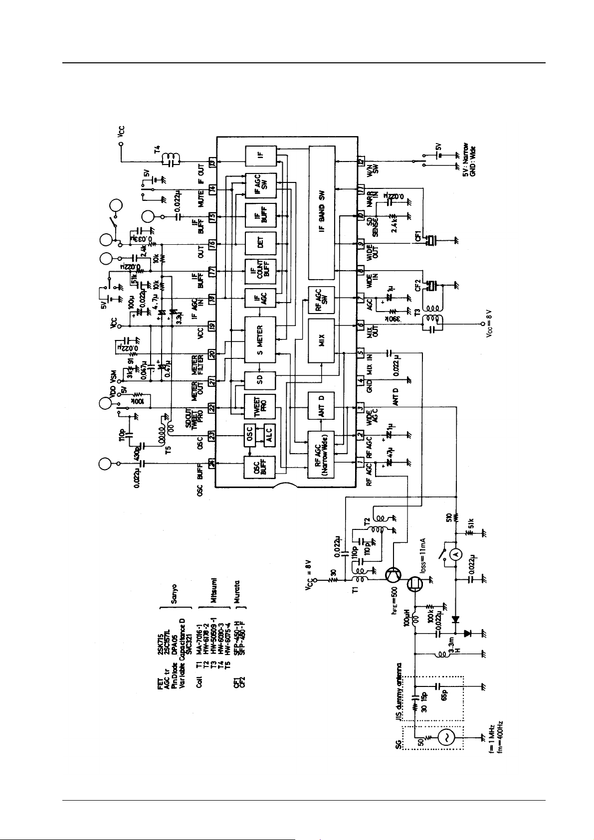
LA1136N, LA1136NM Test Circuit
Distortion meter
High frequency
signal level meter
IHF signal level meter
with bandpass filter
High frequency
signal level meter
Unit (resistance: Ω, capacitance: F)
S-meter output
Voltmeter
High frequency
signal level meter
No. 3507-5/28
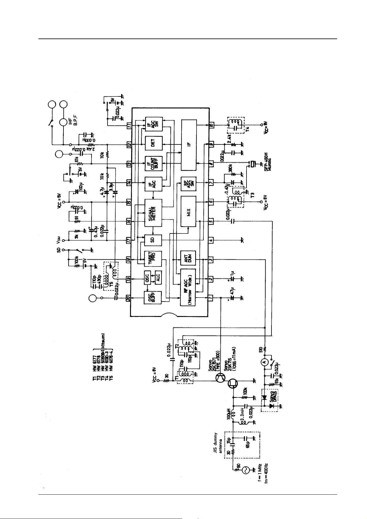
LA1136N, 1136NM, 1137N, 1137NM
LA1137N, LA1137NM Test Circuit
Distortion meter
Signal meter
VHF signal
meter
Unit (resistance: Ω, capacitance: F)
S-meter output
VHF signal
meter
No. 3507-6/28
LA1136N Equivalent Circuit
LA1136N, 1136NM, 1137N, 1137NM
No. 3507-7/28

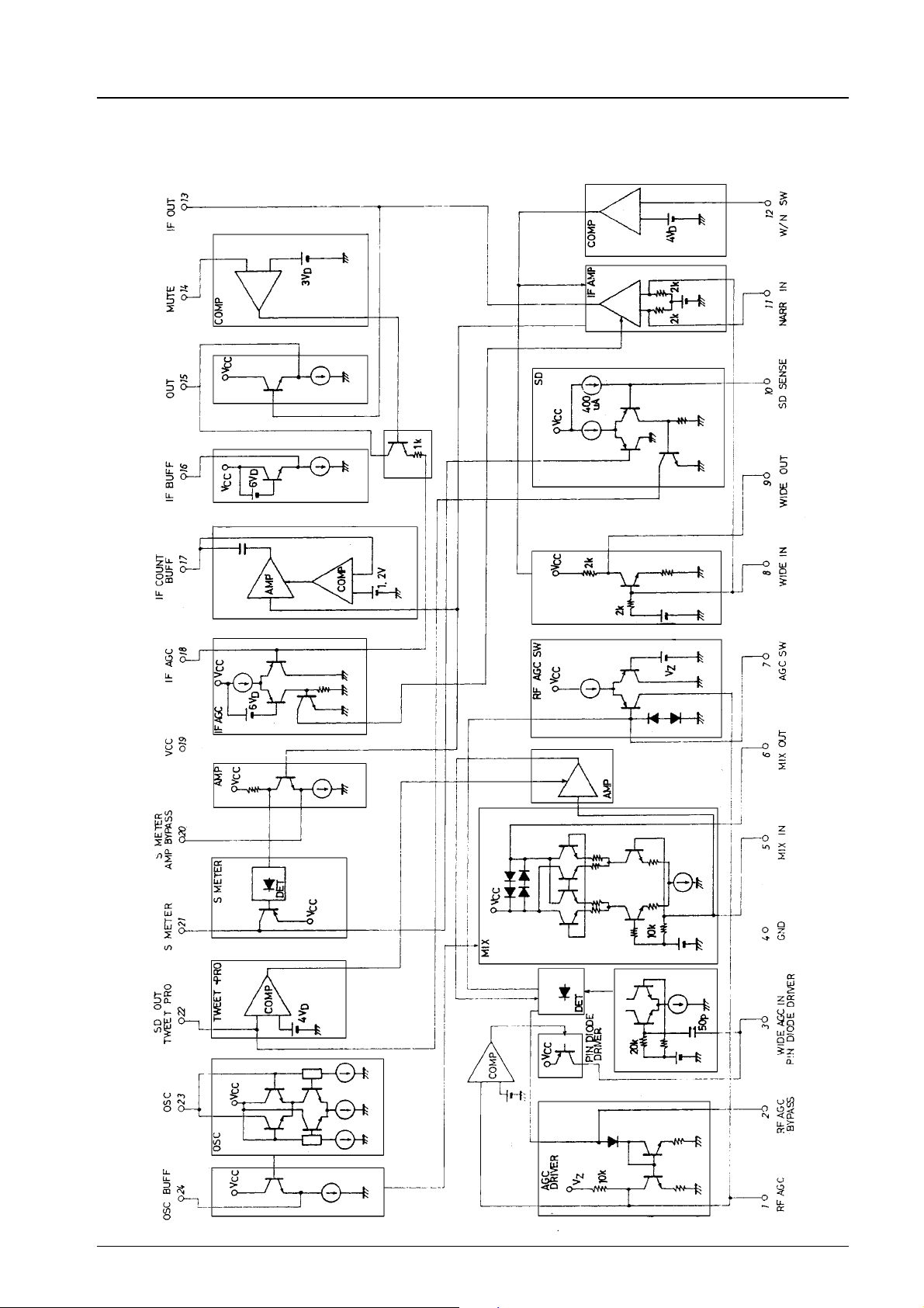
LA1137N Equivalent Circuit
LA1136N, 1136NM, 1137N, 1137NM
No. 3507-8/28
LA1136N, 1136NM, 1137N, 1137NM
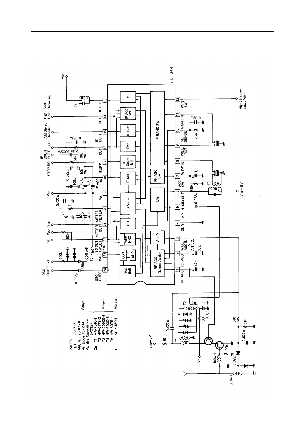
LA1136N Sample Application Circuit
Unit (resistance: Ω, capacitance: F)
Pins connected to the controller
.
LA1136N
No. 3507-9/28
 Loading...