

SANYO LA1135, LA1135M Datasheet
Ordering number: EN1272E
Monolithic Linear IC
LA1135, 1135M
AM Tuner System for
Car Radios and Home Stereos
Overview
The LA1135 is a high-performance AM electronic tuner IC that
is greatly improved in cross modulation characteristics. It is
especially suited for use in car radio and home stereo (antenna:
loop) applications.
Functions
.
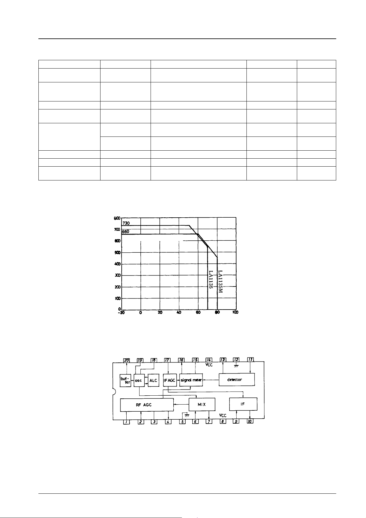
MIX
.
OSC (with ALC)
.
IF amplifier
.
Detector
.
AGC (normal)
.
RF wide-band AGC
.
Auto search stop signal (signal meter output)
.
Local oscillation buffer output
.
Others
Features
.
Excellent cross modulation characteristics: Meets the
requirements for preventing not only adjacent-channel
interference but also interference caused by all channels
within broadcast band.
.
Narrow-band signal meter output: Usable as auto search stop
signal. Has linearity up to 80 dBµ.
.
Local oscillation buffer output: Facilitates designing of
electronic tuner system, frequency display, etc.
.
OSC (with ALC): Improves tracking error because
oscillation output is stabilized at a low level (380 mVrms)
for varactor diode.
.
MIX: Double-balanced differential MIX meeting the
requirements for preventing spurious interference, IF
interference.
.
Good characteristics at high input: 130 dBµ input
f
= 400 Hz 80% mod THD = 0.4% typ
m
.
Low noise: Good S/N at medium input (56 dB typ)
.
Usable sensitivity: (S/N = 20 dB input): 25 dBµ (2SK315
I
= 11mA)
DSS
.
VCCvariation compensation: Less variation in gain,
distortion: 8 to 12 V
.
Reduced pop noise: Capable of reducing pop noise at the
time of V
constant.
ON, mode select by adjusting AGC time
CC
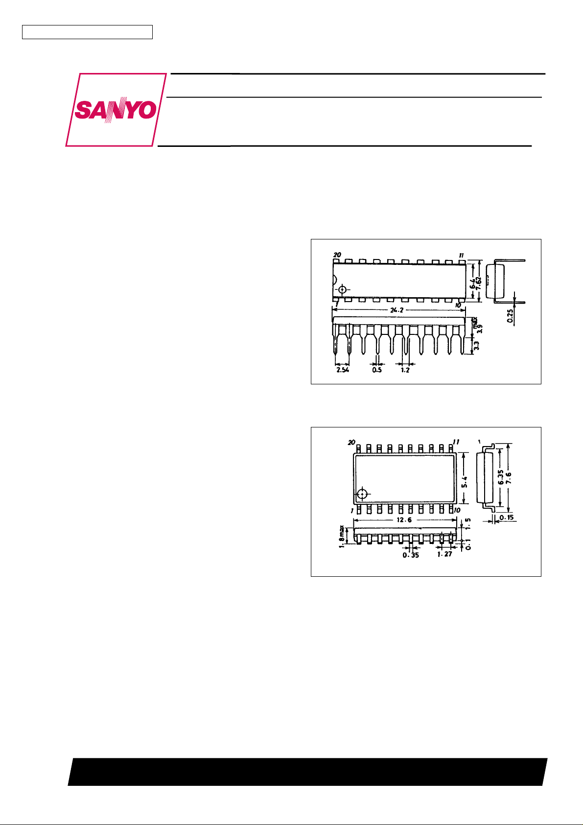
Package Dimensions
unit : mm
3021B-DIP20S
[LA1135]
SANYO : DIP20S
unit : mm
3036B-MFP20
[LA1135M]
SANYO: MFP20
SANYO Electric Co.,Ltd. Semiconductor Bussiness Headquarters
TOKYO OFFICE Tokyo Bldg., 1-10, 1 Chome, Ueno, Taito-ku, TOKYO, 110 JAPAN
93097HA(II)/D0994JN/O217KI/4034KI.TS(KOTO) No.1272-1/18
LA1135, 1135M
Specifications
Maximum Ratings at Ta = 25°C
Parameter Symbol Conditions Ratings Unit
Maximum supply voltage V
Output voltage V
Input voltage V
Current drain I
Flow-out current I
Allowable power
dissipation
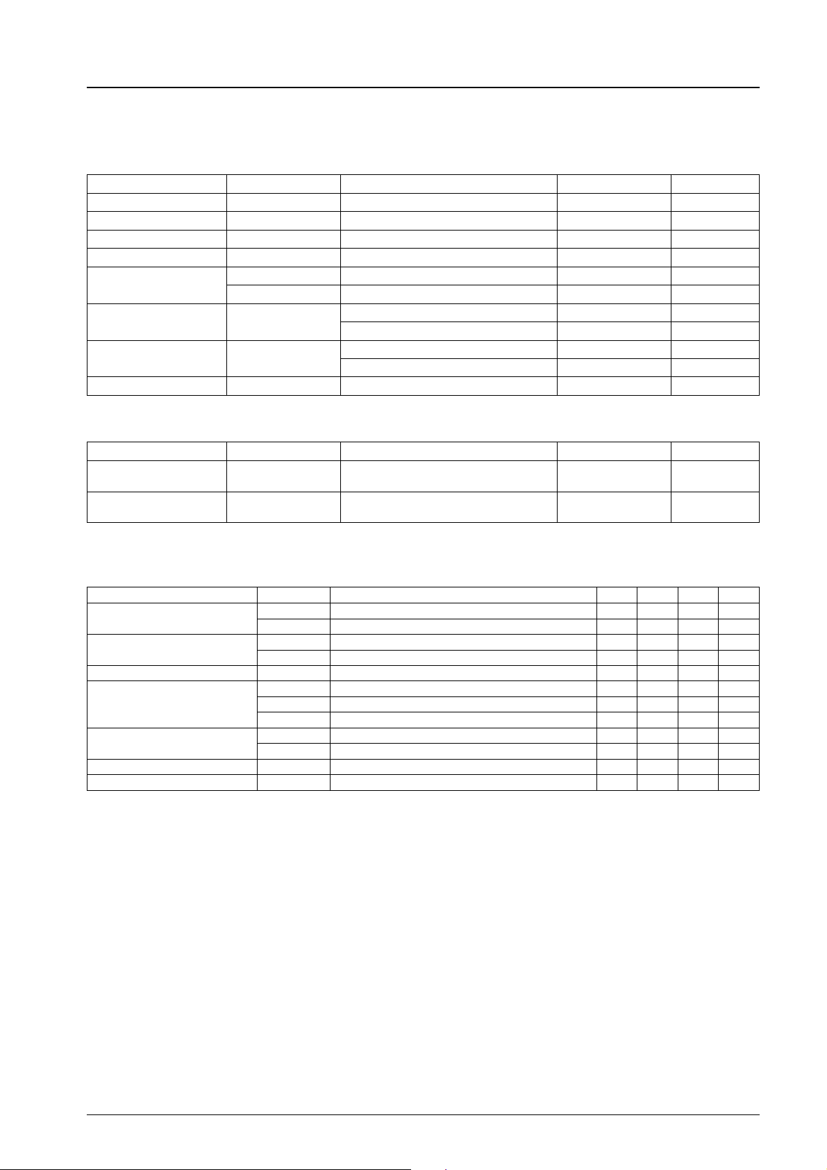
Operating temperature Topr LA1135 –20 to +70 °C
Storage temperature Tstg –40 to +125 °C
Operating Conditions at Ta = 25°C
Parameter Symbol Conditions Ratings Unit
Recommended supply
voltage
Operating supply voltage
range
max Pins 8, 14 16 V
CC
O
IN
CC
18
I
20
Pd max LA1135 730 mW
V
CC
V
op 7.5to12 V
CC
Pins 7, 10 24 V
Pin 6 5.6 V
Pins7+8+10+14 41 mA
Pin 18 2 mA
Pin 20 2 mA
LA1135M Ta % 60°C, with PCB 660 mW
LA1135M –40 to +80 °C
8V
Operating Characteristics at Ta = 25°C, VCC=8V,fr= 1 MHz, fm= 400 Hz, See specified Test
Circuit.
Parameter Symbol Conditions min typ max Unit
I
1 Quiescent 13.5 22.5 32.5 mA
Current drain
Detection output
Signal-to-noise ratio S/N 74 dBµ input, 30% mod 51.0 56.0 dB
Total harmonic distortion
Signal meter output
Input at signal meter output 1 V V
Local oscillation buffer output V
CC
I
2 130 dBµ input 20.0 30.0 41.0 mA
CC
V
1 16 dBµ input, 30% mod –29.0 –25.0 –21.0 dBm
O
V
2 74 dBµ input, 30% mod –15.0 –12.0 –9.0 dBm
O
THD1 74 dBµ input, 30% mod 0.3 1.0 %
THD2 74 dBµ input, 80% mod 0.3 1.0 %
THD3 130 dBµ input, 80% mod 0.4 2.0 %
V
1 Quiescent 0 0.3 V
SM
V
2 130 dBµ input 3.5 5.0 7.5 V
SM
1VSM= 1 V 18.0 24.0 30.0 dBµ
IN
BUF 320 380 mVrms
OSC
No. 1272-2/18
LA1135, 1135M
Reference Characteristics
Parameter Symbol Conditions typ Unit
Usable sensitivity Q.S. Input at S/N = 20 dB
Wide-band AGC
ON-state input
Detection output variation ∆V
Local oscillation variation
within broadcast band
Signal meter band * V
Selectivity 30 % mod ±10 kHz * 43 dB
IF interference IF. R. f
Image frequency
interference
O
∆V
OSC
SM-BW1
V
SM-BW2
IM. R. f
(2SK315 I
Reception 1.0 MHz quiescent
Interference 1.4 MHz non-mod
at input for AMT.D. ON
Input 74 dBµ → 130 dBµ 0.2 dB
V
L–V
OSC
74 dBµ input, frequency at
which output is reduced to 1/2
74 dBµ input, frequency at
which output is reduced to 1/10
= 600 kHz * 77.5 dB
r
= 1400 kHz * 52.0
r
=11mA)
DDS
H 15 mVrms
OSC
Note: *: Wide-band AGC OFF
( ): See circuit on page 7.
25.0 dBµ
82.0 dBµ
±1.5 kHz
–4.5/+7 kHz
(63.0)
dB
with 54 × 34 × 1.7 mm3PCB
Allowable power dissipation, Pd max – mW
Ambient temperature, Ta – °C
Equivalent Circuit Block Diagram
Pd max – Ta
No. 1272-3/18
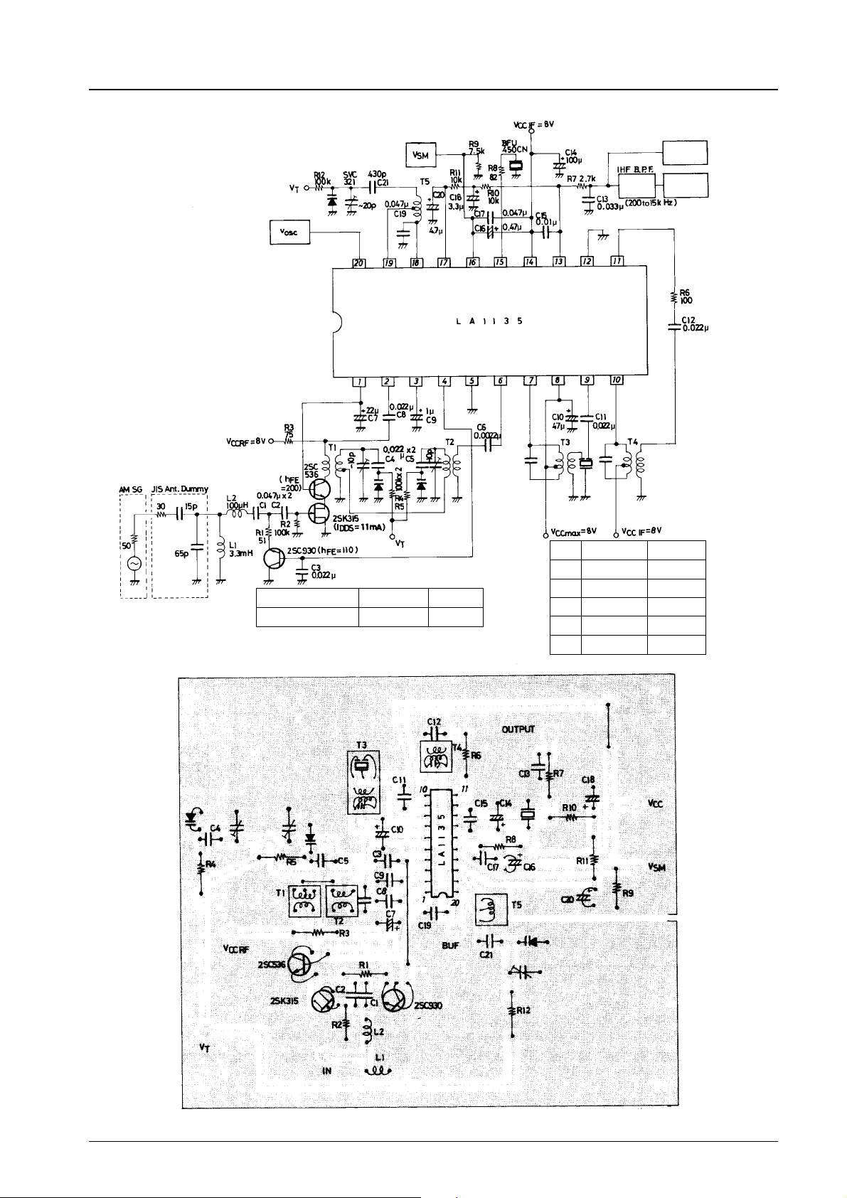
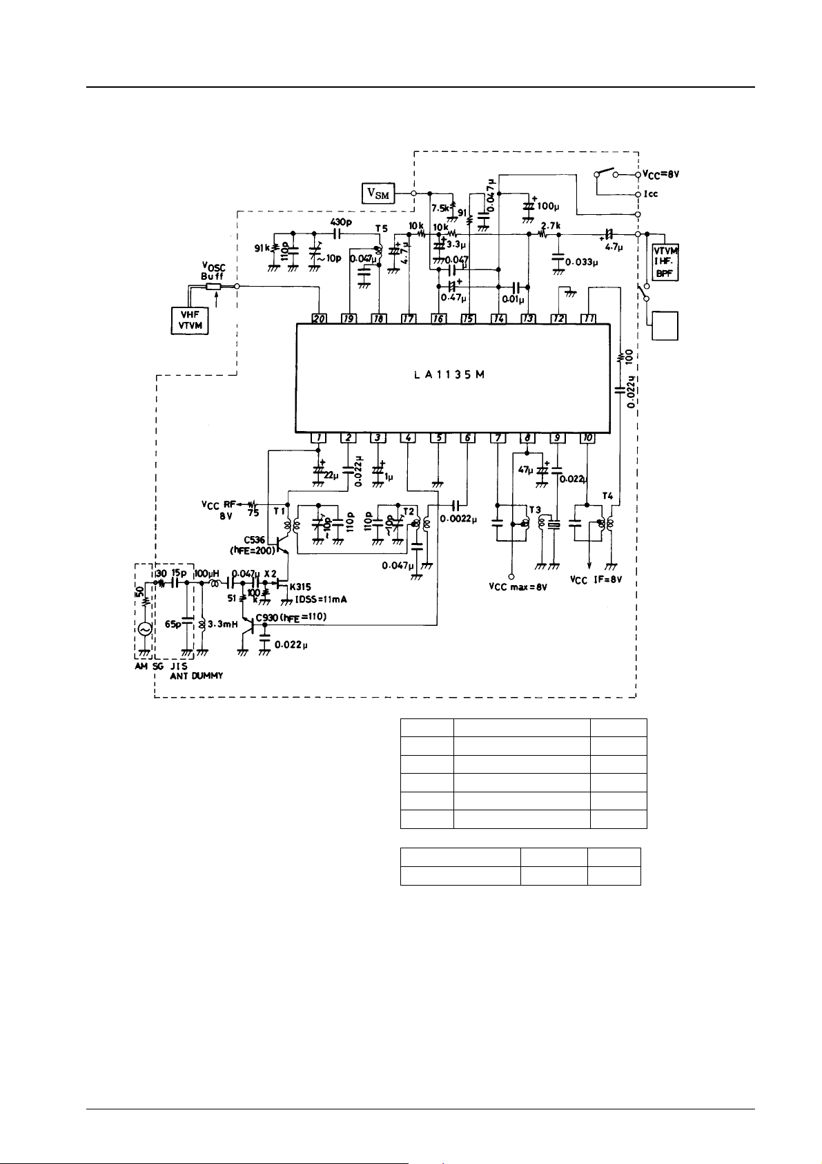
Test Circuit 1
VCC=8V,fr= 1 MHz, fm= 400 Hz
Unit (resistance: Ω, capacitance: F)
HF valve voltmeter
LA1135, 1135M
DC voltmeter
Distortion
meter
Valve
voltmeter
V
O
Varactor diode SVC321 (Sanyo)
Narrow-band filter BFU450CN (Murata)
Sample Printed Circuit Pattern
Coil
T1 YT-30020 (Mitsumi)
T2 YT-30018 (Mitsumi)
T3 CFMA-027 (Toko)
T4 YT-30007 (Mitsumi)
T5 YT-30008 (Mitsumi)
Cu-foiled area 105 × 120 mm
2
No. 1272-4/18
Test Circuit 2
VCC=8V,fr= 1 MHz, fm= 400 Hz
LA1135, 1135M
DC voltmeter
Detection output
Probe load open
Distortion meter
Unit (resistance: Ω, capacitance: F)
Coil
T1 YT-30202 (Mitsumi)
T2 YT-30018 (Mitsumi)
T3 CFMA-021A (Toko)
T4 YT-30007 (Mitsumi)
T5 YT-30008 (Mitsumi)
Varactor diode SVC321 (Sanyo)
Narrow-band filter BFU450CN (Murata)
No. 1272-5/18
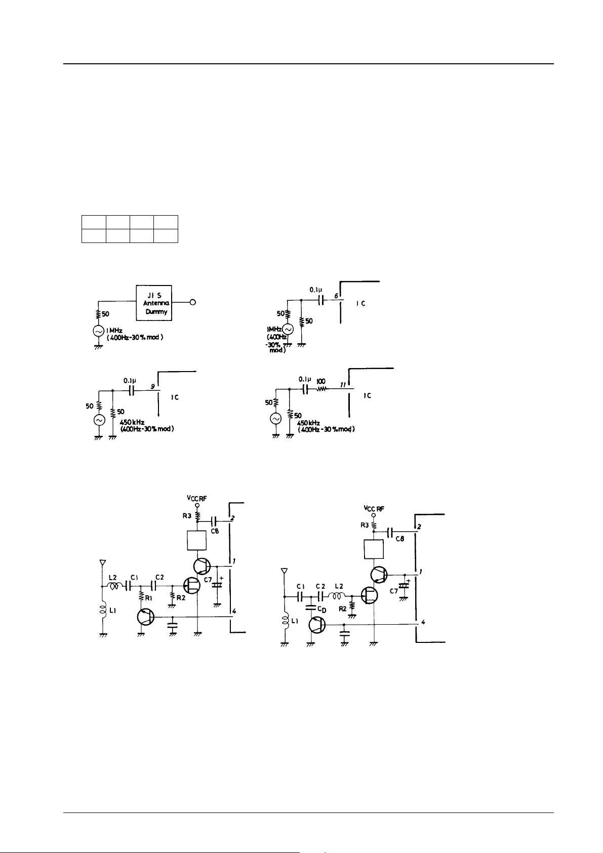
Proper cares in using IC
LA1135, 1135M
1. Bias condition: RF VCC% IF V
CC
2. Avoid coupling between the antenna tuning circuit and the local oscillation.
3. Connect detection capacitor C15 across pins 13 (output) and 14 (V
) so that no leakage of the IF signal to the GND line
CC
occurs. (If connected to GND, the tweet and the usable sensitivity may get worse.) Radiation from C15 may cause harmonics
in the IF signal to return to the RF stage, thereby leading to more tweet interference. So, connect C15 as close to pins 13, 14
as possible. Consider the direction of the capacitor and separate it from the ANT circuit.
4. For R9, use a semifixed resistor with V
considered.
SM
5. When designing the coils, consider the following conditions.
Shown below is the input level at each pin at which the detection output at f
ANT MIX IF Det
16.0 28.0 45.0 61.0
(dBµ)
= 400 Hz 30% mod becomes –25 dB.
m
How to apply input to each stage
ANT stage
MIX stage
ANT input
IF stage
Det stage
Unit (resistance: Ω, capacitance: F)
6. ANT damping
To make the ANT damping constant within the receiving band, change the application circuit as shown below.
Old circuit New circuit
Double tuning
Double tuning
Measures
Replace R1 with C
C
(2000 pF to 3000 pF or thereabouts)
D
.
D
Relocate L2.
Damping (600 kHz to 1400 kHz) Old circuit –15 dB
New circuit –4 dB
No. 1272-6/18
 Loading...