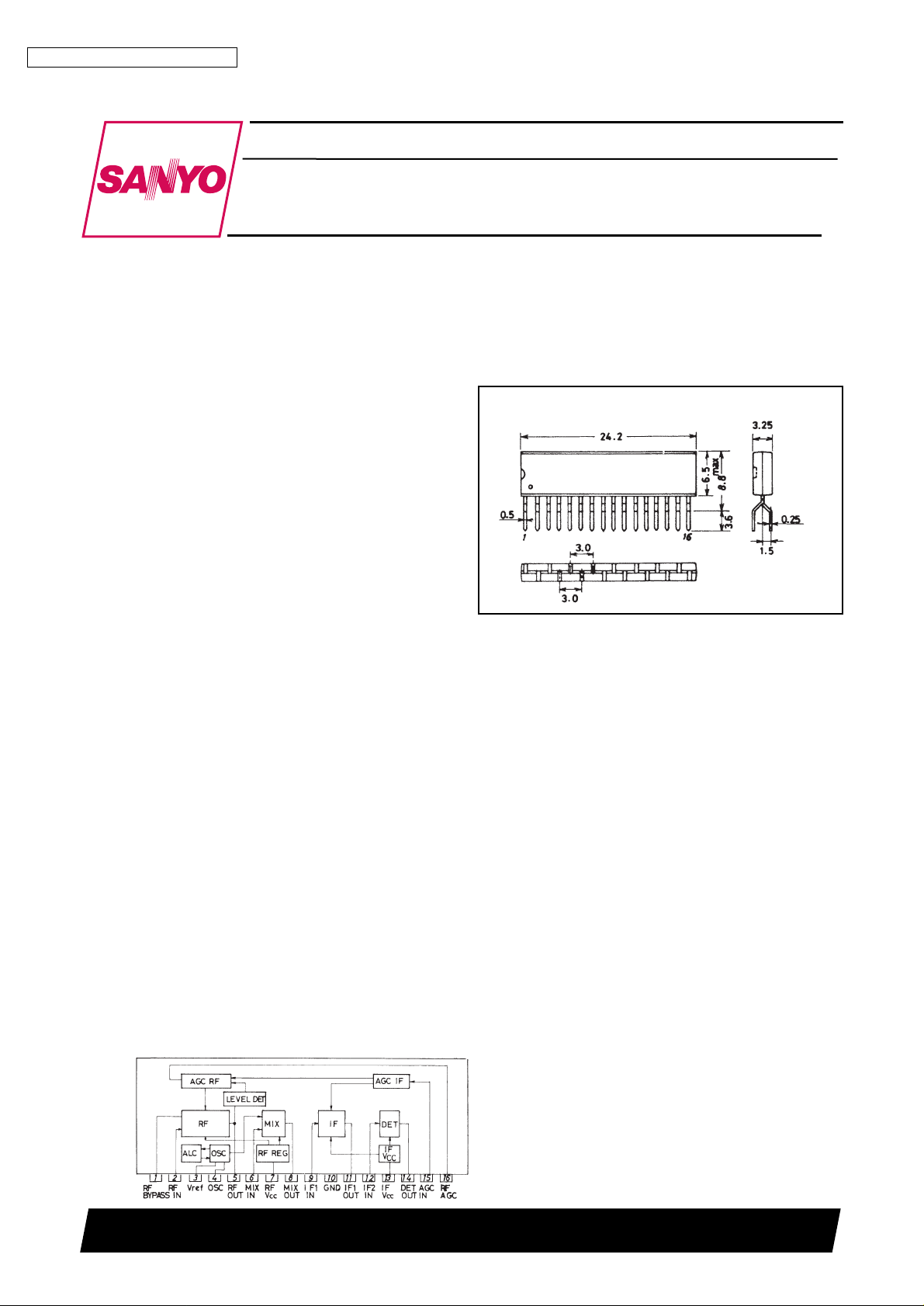
SANYO LA1130 Datasheet

LA1130
Ordering number : EN595C
AM Tuner for Car Radio
Monolithic Linear IC
SANYO Electric Co.,Ltd. Semiconductor Bussiness Headquarters
TOKYO OFFICE Tokyo Bldg., 1-10, 1 Chome, Ueno, Taito-ku, TOKYO, 110 JAPAN
93097HA (KT)/2248KI/D147KI/4105MW/3163KI, ki No.595-1/5
Overview
The LA1130 is an IC developed for AM tuner systems in
car radio applications. It provides low-level local
oscillation so that it can be applied in varactor diode tuning
applications as well as µ tuning applications.
Functions
• RF amplification
• MIX
• OSC (with ALC)
• IF amplification
• Detection
• AGC (normal)
• RF wide-band AGC
• Others
Package Dimensions
unit: mm
3020A-SIP16
[LA1130]
SANYO: SIP16
Features
• Good space factor due to single-end package.
• Easy to design printed circuit pattern due to 3mm-pitch pin interval.
• Double-balanced type MIX : Improvement in IF interference, spurious interference.
• Normal AGC : Less variation in detector output to input.
• RF wide-band AGC : Improvement in cross modulation distortion, especially strong input characteristics in
varactor diode tuning applications because of low operating level (300mVrms).
• AGC drive output for FET : Possible to apply AGC to FET at input stage in varactor diode tuning applications.
• ALC at OSC stage : Improvement in tracking error due to stabilized low-level (350mVrms) oscillation output
in varactor diode tuning applications.
• Reference voltage output : Possible to use 5.6V reference voltage for other bias (FET, etc.).
•VCCvariation compensation : Less variation in gain, distortion, etc. (7.5 to 16V)
• Less ripple voltage : Less modulation of carrier by supply voltage ripple.
• Low pop noise : Possible to reduce pop noise at the time of VCC-on, mode-on by selecting AGC time
constant.
Equivalent Circuit Block Diagram

Specifications
Maximum Ratings
at Ta=25°C, See specified Test Circuit.
Parameter Symbol Conditions Ratings Unit
Maximum supply voltage VCCmax Pins 7, 13 16 V
Maximum output voltage V
O5
Pin 5 17 V
VO8,
11
Pins 8, 11 24 V
Maximum input voltage VINmax Pin 2 5.6 V
Maximum supply current ICCmax Total of current at pins 5, 7, 8, 11, 13 35 mA
Maximum flow-out current I
3
Pin 3 6 mA
Allowable power dissipation Pd max Ta≤45°C 520 mW
Operating temperature Topr –20 to +70 °C
Storage temperature Tstg –40 to +125 °C
Recommended Operating Condition at Ta=25°C
Parameter Symbol Conditions Ratings Unit
Recommended supply voltage V
CC
7.5 to 14.0 V
Operating Characteristics at Ta=25°C, V
CC
=8V, fr=1MHz, fm=400Hz, See specified Test Circuit.
Parameter Symbol Conditions
Ratings
min typ max
Unit
Current drain ICC1 Quiescent 12.5 18.0 24.5 mA
ICC2 120dBµ input 14.0 20.0 26.5 mA
Detection output VO1 24dBµ input, 30% mod. –31.0 –26.5 –12.0 dBm
VO2 74dBµ input, 30% mod. –18.0 –15.5 –12.0 dBm
Signal to noise ratio S/N 1 24dBµ input, 30% mod. 16 20 dB
S/N 2 74dBµ input, 30% mod. 46 50 dB
Total harmonic distortion THD1 74dBµ input, 30% mod. 0.35 1.0 %
THD2 74dBµ input, 80% mod. 0.35 1.5 %
THD3 120dBµ input, 30% mod. 0.35 2.0 %
RF AGC voltage (V16) V
RFAGC1
Quiescent 5.2 5.6 5.9 V
[Reference characteristics]
Signal to noise ratio S/N 3 35dBµ input, 30% mod. 31 dB
Total harmonic distortion THD4 128dBµ input, 80% mod. 0.58 %
Detection output variation ∆V
O
VO(128dBµ)/VO(74dBµ) 0.4 dB
Bandwidth (6dB) BW
6
6dB width, 15dBµ input 30% mod. 7 kHz
(60dB) BW
60
60dB width, 15dBµ input 30% mod. 30 kHz
Selectivity (1 signal) ACA ±10kHz detuning, 15dBµ input, 40 dB
30% mod.
Ripple rejection ratio 100dBµ input, IF VCC (pin 13) ripple 40.5 dB
level 50Hz to 15dBm
Local oscillation voltage Vosc 350 mVrms
Local osc drift ∆Vosc VoscL(515kHz) to VoscH(1660kHz) 20 mVrms
Whistle 2f
iTweet
74dBµ input, 400Hz beat max. –33 dB
RF AGC voltage (V16) V
RFAGC2
120dBµ input 1 V
RF output voltage V
ORF
100dBµ input, ±10kHz 300 mVrms
IF interference fr=600kHz, 15dBµ input 91.5 dB
Image frequency interference fr=1400kHz, 15dBµ input 70.5 dB
LA1130
No.595-2/5
 Loading...