SANYO LA1061M Datasheet

LA1061M
Ordering number : EN3044A
Antenna Switching Controller
Monolithic Linear IC
SANYO Electric Co.,Ltd. Semiconductor Bussiness Headquarters
TOKYO OFFICE Tokyo Bldg., 1-10, 1 Chome, Ueno, Taito-ku, TOKYO, 110 JAPAN
82997HA (KT)/9070TA/6019TA, TS No.3044-1/8
Overview
The LA1061M is an antenna switching controller for
mobile radio equipment.
The LA1061M uses a number of inputs from the receiver
circuitry to select the main antenna or sub-antenna
according to signal strength and quality. Weak and strong
signals are detected with the S-meter DC voltage and F.E.
AGC voltage, respectively. Multi-path distortion is
detected from the AC component of the IF output, using
the same high-sensitivity counter circuit as in Sanyo's
earlier LA1060 device. An auxiliary circuit keeps the main
antenna selected for a fixed time period when reception
conditions outside a moving vehicle are changing rapidly.
The LA1061M is available in surface-mount 8-pin DIPs,
facilitating construction of compact equipment. It operates
from a single 7 to 12V power supply.
Package Dimensions
unit: mm
3111-MFP14S
[LA1061M]
SANYO: MFP14S
Features
• Uses Sanyo's proprietary AGC amplifier and detector, providing accurate detection of multi-path distortion.
• High-current Main and Sub-antenna switching outputs.
• Antenna switching frequency limiting circuit.
• On-board comparators for F.E AGC (strong signal) and S-meter DC (weak signal) detection.
• Surface-mount 14-pin MFP.
Specifications
Maximum Ratings
at Ta=25°C
Parameter Symbol Conditions Ratings Unit
Maximum supply voltage VCCmax 14 V
Allowable power dissipation Pd max 182 mW
Operating temperature Topr –30 to +80 °C
Storage temperature Tstg –40 to +125 °C
Maximum flow-out current I
4
Pin 4 1 mA
I
5
Pin 5 10 mA
I
6
Pin 6 10 mA
I
9
Pin 9 2 mA
I
10
Pin 10 5 mA
I
12
Pin 12 2 mA
Maximum apply voltage V
13
Pin 13 V
CC
V
V
14
Pin 14 V
CC
V

LA1061M
No.3044-2/8
Operating Conditions at Ta=25°C
Parameter Symbol Conditions Ratings Unit
Recommended supply voltage V
CC
8 V
Operating voltage range VCCop 7 to 12 V
Operation Characteristics at Ta=25°C, V
CC
=8V, f=100kHz sine wave
Parameter Symbol Conditions
Ratings
min typ max
Unit
Current drain I
CC
No input, I5and I6are not included. 4.5 7 12 mA
Pin 5 ‘H’-level voltage V
5
1kΩ to ground 5.0 6.0 7.0 V
Pin 6 ‘H’-level voltage V
6
1kΩ to ground 5.0 6.0 7.0 V
Noise amp gain Gv1 VIN=3mVrms, f=100kHz 33 36 39 dB
Gv2 VIN=100mVrms, f=100kHz 10 13 16 dB
Noise detection sensitivity NDS Noise AGC off 9 12 15 mVrms
Noise count number NCN VIN=30mVrms, f=100kHz, sine wave 10
Gate time 1 tG1 Noise AGC off 120 150 180 µs
Pin 9 voltage V
9
VIN=100mVrms, f=100kHz, 7.0 7.7 8.0 V
R9=300kΩ
Strong signal comparator V
th14
0.8 1.0 1.2 V
threshold
Weak signal comparator V
th13
1.8 2.0 2.2 V
threshold
Gate time 2 tG2 2 4 6 ms
Gate time3 tG3 13 23 40 ms
Switching frequency HCN 15
limit maximum count
Equivalent Circuit Block Diagram
Unit (resistance : Ω)

LA1061M
No.3044-3/8
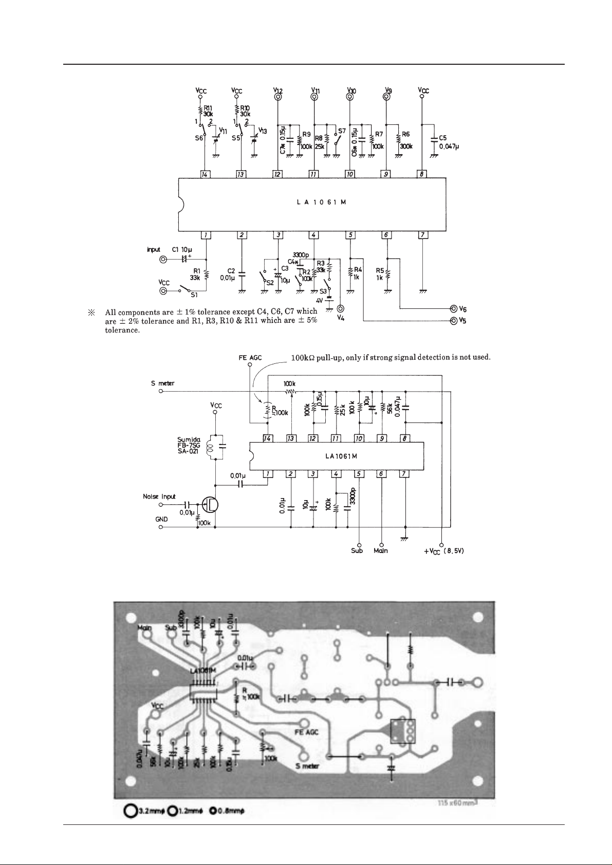
Operating Characteristic Test Circuit
Sample Printed Circuit Pattern
Sample Application Circuit
Unit (resistance : Ω, capacitance : F)
Unit (resistance : Ω, capacitance : F)
 Loading...