SANYO LA1060 Datasheet

LA1060
Ordering number : EN2650B
Antenna Switching Diversity Circuit
for Car-Use FM Tuners
Monolithic Linear IC
SANYO Electric Co.,Ltd. Semiconductor Bussiness Headquarters
TOKYO OFFICE Tokyo Bldg., 1-10, 1 Chome, Ueno, Taito-ku, TOKYO, 110 JAPAN
82997HA (KT)/7119YT/D147TA/N196AT, TS No.2650-1/8
Functions
• Noise amp, noise AGC circuit, noise density circuit.
• Antenna switching trigger output circuit.
• Antenna switching T flip-flop circuit.
• Antenna holding function to be used at weak input signal
reception mode, forced antenna holding function.
Features
• "Count system"-used, reliable detection of multipath
distortion.
• One-tuner type diversity system allowing cost reduction
of sets.
• The output to hold the antenna at the weak input signal
mode and the output (antenna switching trigger output) to
indicate that the antenna switching frequency is high are
delivered at the same pin, allowing a wide variety of
applications according to the design concept of set.
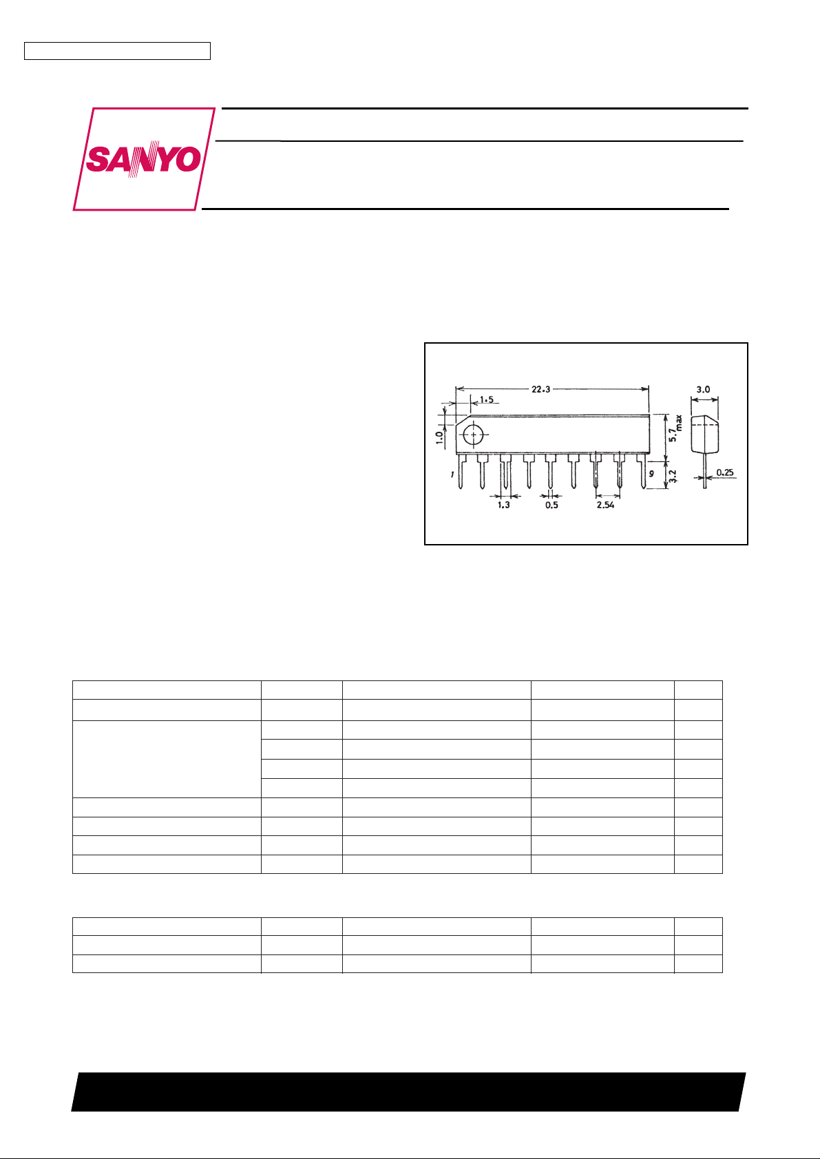
Package Dimensions
unit: mm
3017B-SIP9
[LA1060]
SANYO: SIP9
Specifications
Maximum Ratings
at Ta=25°C
Parameter Symbol Conditions Ratings Unit
Maximum supply voltage VCCmax 16 V
Maximum flow-out I4max 1 mA
I6max 2 mA
I7max 10 mA
I8max 10 mA
Maximum flow-in current I6max 10 mA
Allowable power dissipation Pd max Ta≤75°C 200 mW
Operating temperature Topr –20 to +75 °C
Storage temperature Tstg –40 to +125 °C
Operating Conditions at Ta=25°C
Parameter Symbol Conditions Ratings Unit
Recommended supply voltage V
CC
8V
Operating voltage range VCCop 6.5 to 15 V

LA1060
Electrical Characteristics at Ta=25°C, V
CC
=8.0V, f=100kHz sine wave
Parameter Symbol Conditions
Ratings
min typ max
Unit
Current drain I
CC
No input, not including pins 3.8 4.9 6.0 mA
7, 8 current
Pin 7 high voltage V7
H
Pin 7-GND resistance=1kΩ 5.0 6.0 7.0 V
Pin 8 high voltage V8
H
Pin 8-GND resistance=1kΩ 5.0 6.0 7.0 V
Noise amp gain VG1 Input=3mVrms *1 33 36 39 dB
VG2 Input=100mVrms *1 10 13 16 dB
Noise detection sensitivity NDS Noise AGC=OFF 9 12 15 mVrms
Input signal level at which the
output at pins 7, 8 starts to be
inverted *2
Number of noise counts NCN Input=30mVrms 10
Number of sine waves which
causes the output at pins 7, 8 to be
inverted *2
Gate time t
G
Noise AGC=OFF 100 120 140 µs
Repetitive period of pin 4 waveform
Pin 6 voltage V6 Input=100mVrms *3 1.6 2.0 2.5 V
Antenna holding HLD Input=100mVrms, noise AGC=OFF 5.0 6.0 7.0 V
Pin 8 output voltage *4
Note
*1 : S1=OFF S2=OFF S3=ON S4=OFF S5=OFF
*2 : S1=OFF S2=ON S3=OFF S4=ON S5=OFF
*3 : S1=OFF S2=OFF S3=OFF S4=ON S5=OFF
*4 : S1=OFF S2=ON S3=OFF S4=ON S5=ON
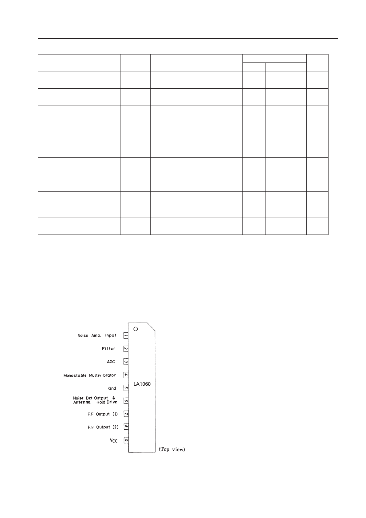
Pin Assignment
No.2650-2/8

LA1060
No.2650-3/8
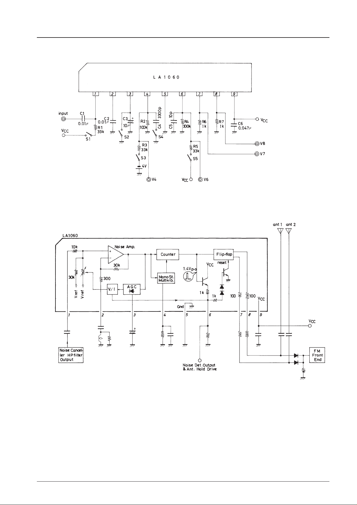
AC Characteristics Test Circuit Diagram
Block Diagram
Unit (resistance : Ω, capacitance : F)
Unit (resistance : Ω, capacitance : F)
 Loading...