

Samsung S3C7414, S3C7424, S3C7434, S3P7414, S3P7424 Datasheet
...
S3C7414/P7414/C7424/P7424/C7434/P7434 PRODUCT OVERVIEW
1 PRODUCT OVERVIEW
OVERVIEW
The S3C7414/C7424/C7434 single-chip CMOS microcontroller has been designed for very high performance
using Samsung's newest 4-bit CPU core, SAM47 (Samsung Arrangeable Microcontroller).
With an A/D converter, LED direct drive pins, an 8-bit serial I/O interface, and an 8-bit timer/counter, the
S3C7414/C7424/C7434 offers you an excellent design solution for a wide variety of home appliance applications
— electric fans, cookers, boilers, and air conditioners, for example.
Up to 35 pins of the 42-pin SDIP or 44-pin QFP package can be dedicated to I/O. Seven vectored interrupts
provide fast response to internal and external events.
In addition, the S3C7414/C7424/C7434's advanced CMOS technology provides for low power consumption and a
wide operating voltage range.
OTP
The S3C7414/C7424/C7434 microcontroller is also available in OTP (One Time Programmable) version,
S3P7414/P7424/P7434. S3P7414/P7424/P7434 microcontroller has an on-chip 4-Kbyte one-time-programmable
EPROM instead of masked ROM. The S3P7414/P7424/P7434 is comparable to S3C7414/C7424/C7434, in
function, in D.C. electrical characteristics and in pin configuration.
DEVELOPMENT SUPPORT
The Samsung Microcontroller Development System, SMDS, provides you with a complete PC-based development environment for S3C7-series microcontrollers that is powerful, reliable, and portable. In addition to its
window-based program development structure, the SMDS toolset includes versatile debugging, trace, instruction
timing, and performance measurement applications.
The Samsung Generalized Assembler (SAMA) has been designed specifically for the SMDS environment and
accepts assembly language sources in a variety of microprocessor formats. SAMA generates industry-standard
hex files that also contain program control data for SMDS compatibility.
1-1

PRODUCT OVERVIEW S3C7414/P7414/C7424/P7424/C7434/P7434
FEATURES SUMMARY
Memory
• 256 × 4-bit RAM
• 4,096 × 8-bit ROM
35 I/O Pins
• I/O: 31 pins including 8 LED direct drive pins
(S3C7414/C7434)
18 pins including 8 LED direct drive pins
(S3C7424)
• Input only: 4 pins
A/D Converter
• 6-channel with 8-bit resolution
• 22.89 µs conversion speed at 4.19 MHz
Basic Timer
• One 8-bit basic timer
• Watchdog timer functions
• Four interval clock selection
Timer/Counters
• Two 8-bit timer/counter (TC0, TC1)
• Programmable 8-bit timer
• External event counter
• Arbitrary clock frequency output
• PWM output mode (TC1)
Watch Timer
• One watch timer 8-bit
• Time interval generation: 0.5 s, 3.9 ms at
4.19 MHz
• Four frequency outputs to BUZ pin
Built-in reset circuit (S3C7434 only)
• Built-in power-on reset circuit
Interrupts
• Five internal vectored interrupts
(INTB, INTT0, INTT1, INTS, INTAD)
• Three external vectored interrupts
(INT0, INT1, INT4)
• Two quasi-interrupts (INT2, INTW)
Bit Sequential Carrier
• Supports 16-bit serial data transfer in
arbitrary format
Memory-Mapped I/O Structure
• Data memory bank 15
Two Power-Down Modes
• Idle mode (only CPU clock stops)
• Stop mode (system oscillation stops)
Oscillation Sources
• Crystal, Ceramic, or RC for system clock
• Crystal, Ceramic: 0.4–6.0 MHz
• RC: 4 MHz (typ)
• CPU clock divider circuit (by 4, 8, or 64)
Instruction Execution Times
• 0.95, 1.91, 15.3 µs at 4.19 MHz
• 0.67, 1.33, 10.7 µs at 6.0 MHz
Operating Temperature
• – 40 °C to 85 °C
8-bit Serial I/O Interface
• 8-bit transmit/receive mode
• 8-bit receive mode
• LSB-first or MSB-first transmission selectable
• Internal or external clock source
1-2
Operating Voltage Range
• 1.8 V to 5.5 V (S3C7414/C7424)
• 2.5 V to 5.5 V (S3C7434)
Package Type
• 42-pin SDIP, 44-pin QFP (S3C7414/C7434)
30-pin SDIP, 28-pin SOP (S3C7424)
S3C7414/P7414/C7424/P7424/C7434/P7434 PRODUCT OVERVIEW
Table 1-1. Comparision Table
Feature S3C7414 S3C7424 S3C7434
Core SAM47 SAM47 SAM47
ROM 4 K bytes Same Same
RAM 256 nibbles Same Same
I/O 35 (4 input only) 21 (3 input only) 35 (4 input only)
POR
(1)
None None Built in/ Typ: 2.0 V
SIO 8-bit SIO x 1 Same Same
Timer0 8-bit timer/counter Same Same
Timer1(PWM) 8-bit timer/counter
Same Same
(8-bit PWM x 1)
Watchdog timer Watch-dog
Same Same
4 selectable interval
ADC 8-bit x 6 8-bit x 4 8-bit x 6
AV
SS
Interrupt External x 3
(2)
None
Internal x 5
Quasi x 2 (KS0–KS3)
Same Same
External x 2
Internal x 5
Quasi x 1 ( – )
External x 3
Internal x 5
Quasi x 2 (KS0–KS3)
Power down Stop/Idle Same Same
Oscillator Crystal, Ceramic, RC Same Same
Operating frequency 0.4–6 MHz Same Same
Operating voltage 1.8–5.5 V 1.8–5.5 V 2.5–5.5 V
OTP/MTP OTP Same Same
Package 42SDIP/44QFP 30SDIP/28SOP 42SDIP/44QFP
NOTES
1. POR (power on reset)/Typ 2.0 V low voltage detector.
2. Internal A/D converter ground (bonded to VSS internally)
1-3
PRODUCT OVERVIEW S3C7414/P7414/C7424/P7424/C7434/P7434
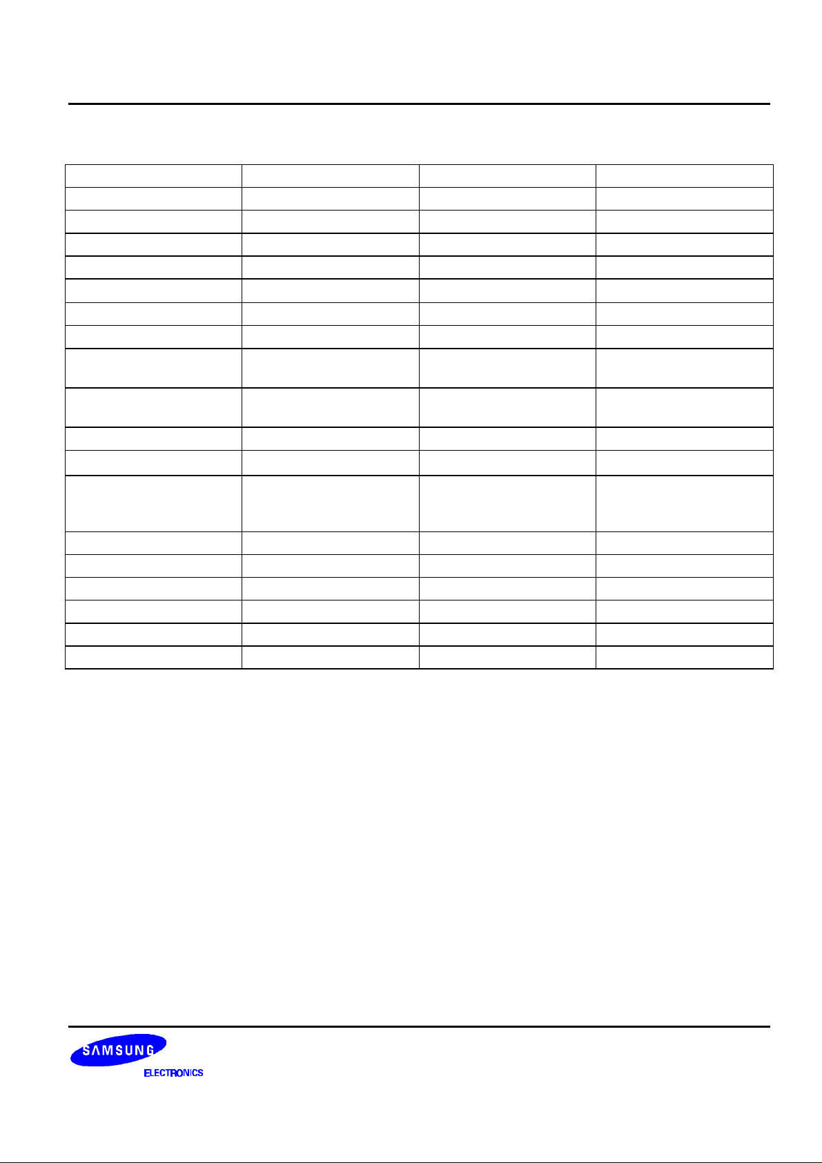
BLOCK DIAGRAM
INT0, INT1, INT2,INT4
COUNTER 0
COUNTER 1
P4.0-4.3
P5.0-5.3
P6.0/KS0
P6.1/KS1
P6.2/KS2
P6.3/KS3
P7.0-7.3 I/O PORT 7
P8.0/TCL0
P8.1/TCLO0
P8.2
I/O PORT 4
I/O PORT 5
I/O PORT 6
I/O PORT 8 I/O PORT 3
8-BIT
TIMER/
8-BIT
TIMER/
RESET
INTERRUPT
CONTROL
BLOCK
INTERNAL
INTERRUPTS
INSTRUCTION DECODER
ARITHMETIC
LOGIC UNIT
256 x 4-BIT
DATA
MEMORY
X
AND
INXOUT
CLOCK
BASIC
TIMER
INSTRUCTION
REGISTER
PROGRAM
COUNTER
PROGRAM
STATUS WORD
STACK
POINTER
4 K BYTE
PROGRAM
MEMORY
WATCH
TIMER
I/O PORT 2
I/O PORT 0
SERIAL
I/O
INPUT
PORT 1
I/O PORT 2
A/D
CONVERTER
P0.0/
SCK
P0.1/SO
P0.2/SI
P0.3/BUZ
P1.0/INT0
P1.1/INT1
P1.2/INT2
P1.3/INT4
P2.0-P2.3/
AD0-AD3
AV
REF
P3.0/AD4
P3.1/AD5
P3.2/CLO/TCL1
P3.3/PWM / TCLO1
1-4
Figure 1-1. S3C7414/C7424/C7434Simplified Block Diagram
S3C7414/P7414/C7424/P7424/C7434/P7434 PRODUCT OVERVIEW
PIN ASSIGNMENTS
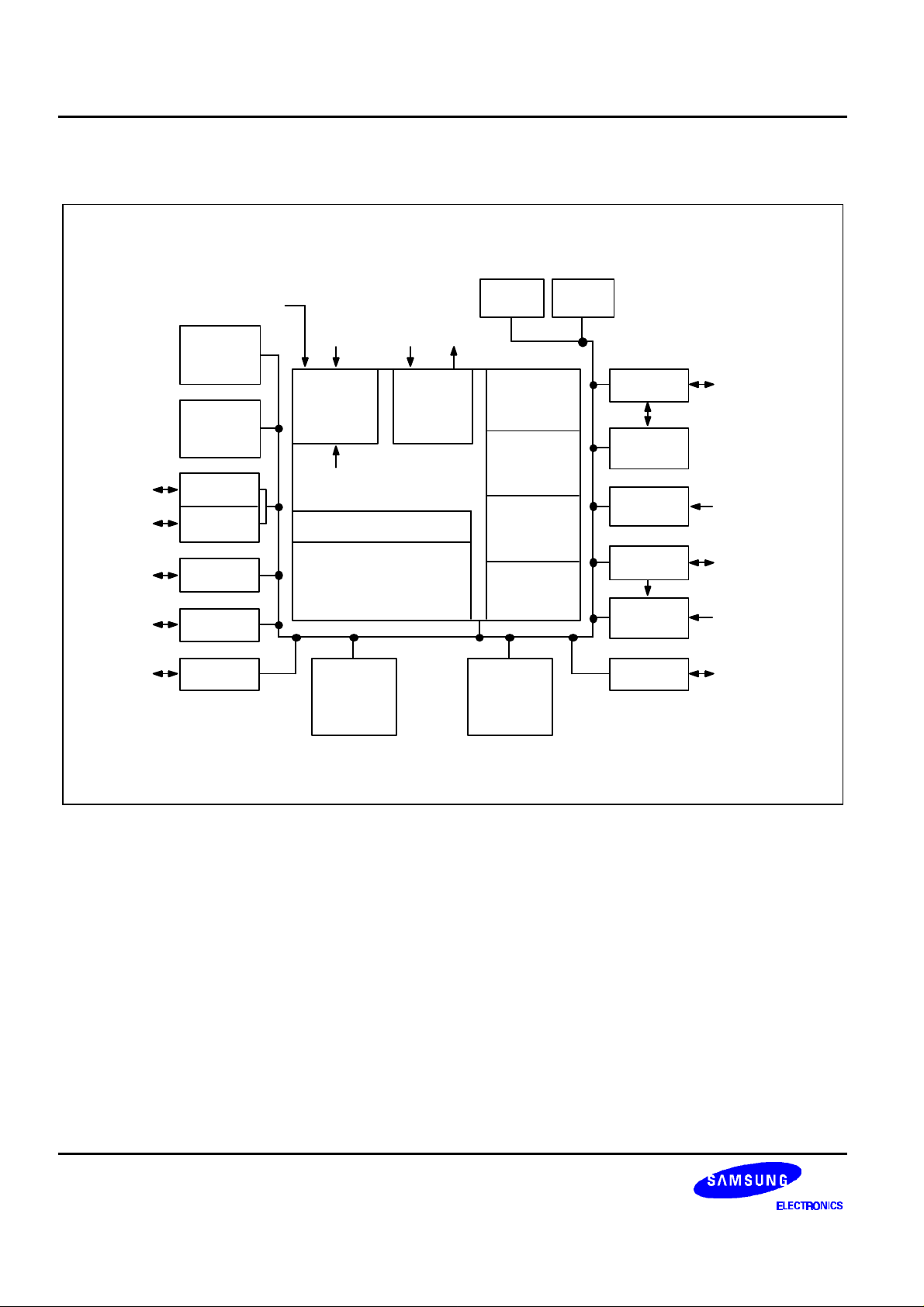
P2.0/AD0
P2.1/AD1
P2.2/AD2
P2.3/AD3
P3.0/AD4
P3.1/AD5
AVREF
P3.2/CLO/TCL1
P3.3/PWM/TCLO1
P4.0
VDD
VSS
XOUT
XIN
TEST
P4.1
P4.2
RESET
P4.3
P5.0
P5.1
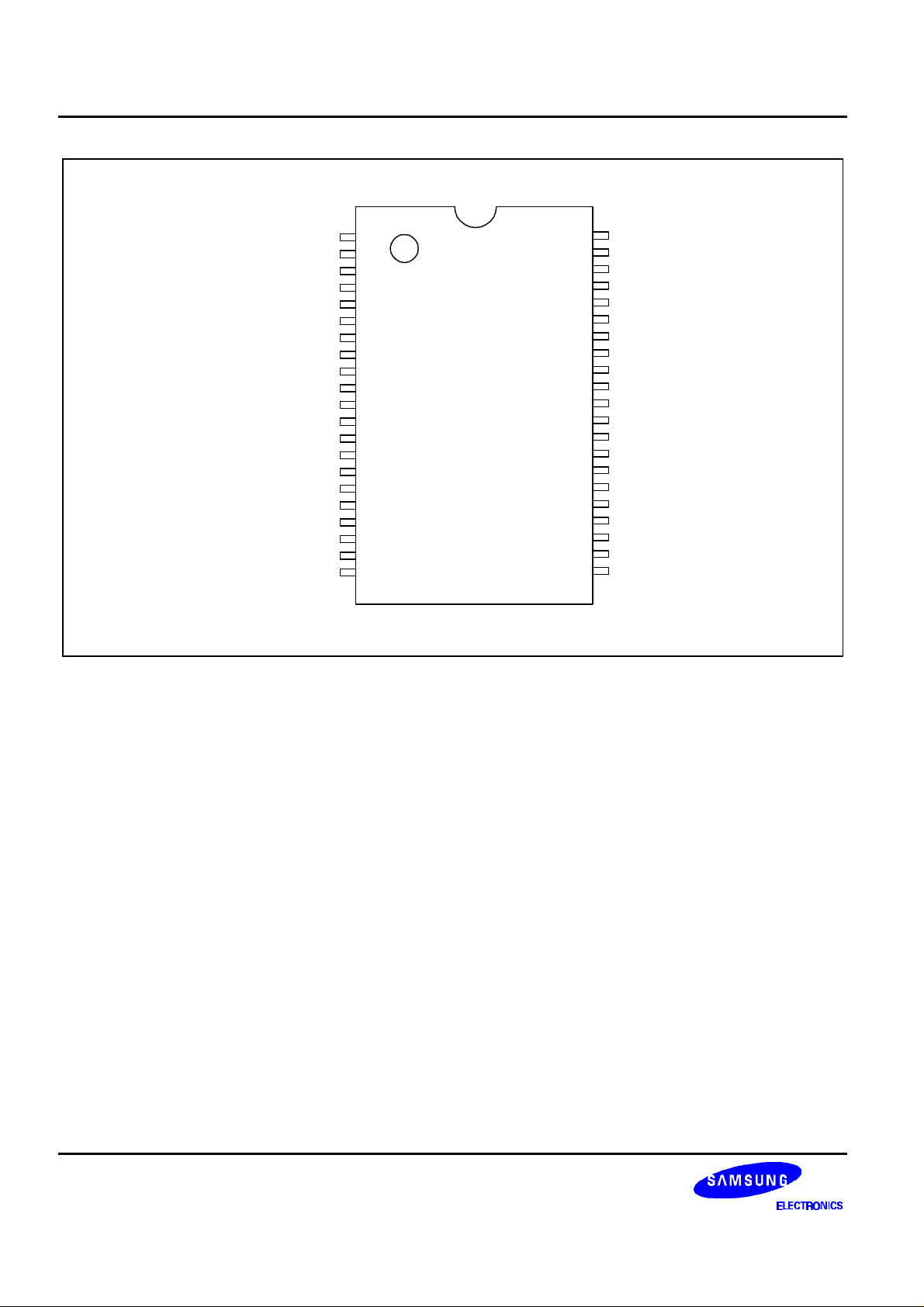
Figure 1-2. S3C7414 Pin Assignment (42-SDIP)
1
2
3
4
5
6
7
8
9
10
11
12
13
14
15
16
17
18
19
20
21
S3C7414
(42-SDIP)
42
41
40
39
38
37
36
35
34
33
32
31
30
29
28
27
26
25
24
23
22
P8.2
P8.1/TCLO0
P8.0/TCL0
P7.3
P7.2
P7.1
P7.0
P6.3/KS3
P6.2/KS2
P6.1/KS1
P6.0/KS0
P1.3/INT4
P1.2/INT2
P1.1/INT1
P1.0/INT0
P0.3/BUZ
P0.2/SI
P0.1/SO
P0.0/SCK
P5.3
P5.2
1-5
PRODUCT OVERVIEW S3C7414/P7414/C7424/P7424/C7434/P7434
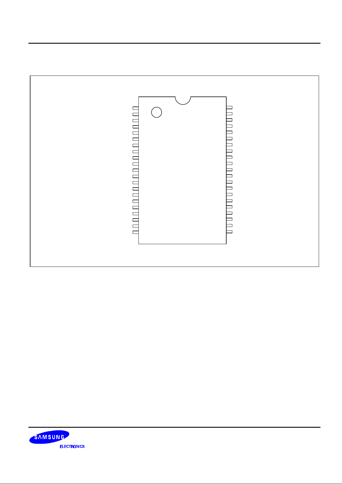
NC
P3.1/AD5
P3.0/AD4
P2.3/AD3
P2.2/AD2
P2.1/AD1
P2.0/AD0
P8.2
P8.1/TCLO0
P8.0/TCL0
P7.3
AVREF
P3.2/CLO/TCL1
P3.3/PWM/TCLO1
P4.0
VDD
VSS
XOUT
XIN
TEST
P4.1
P4.2
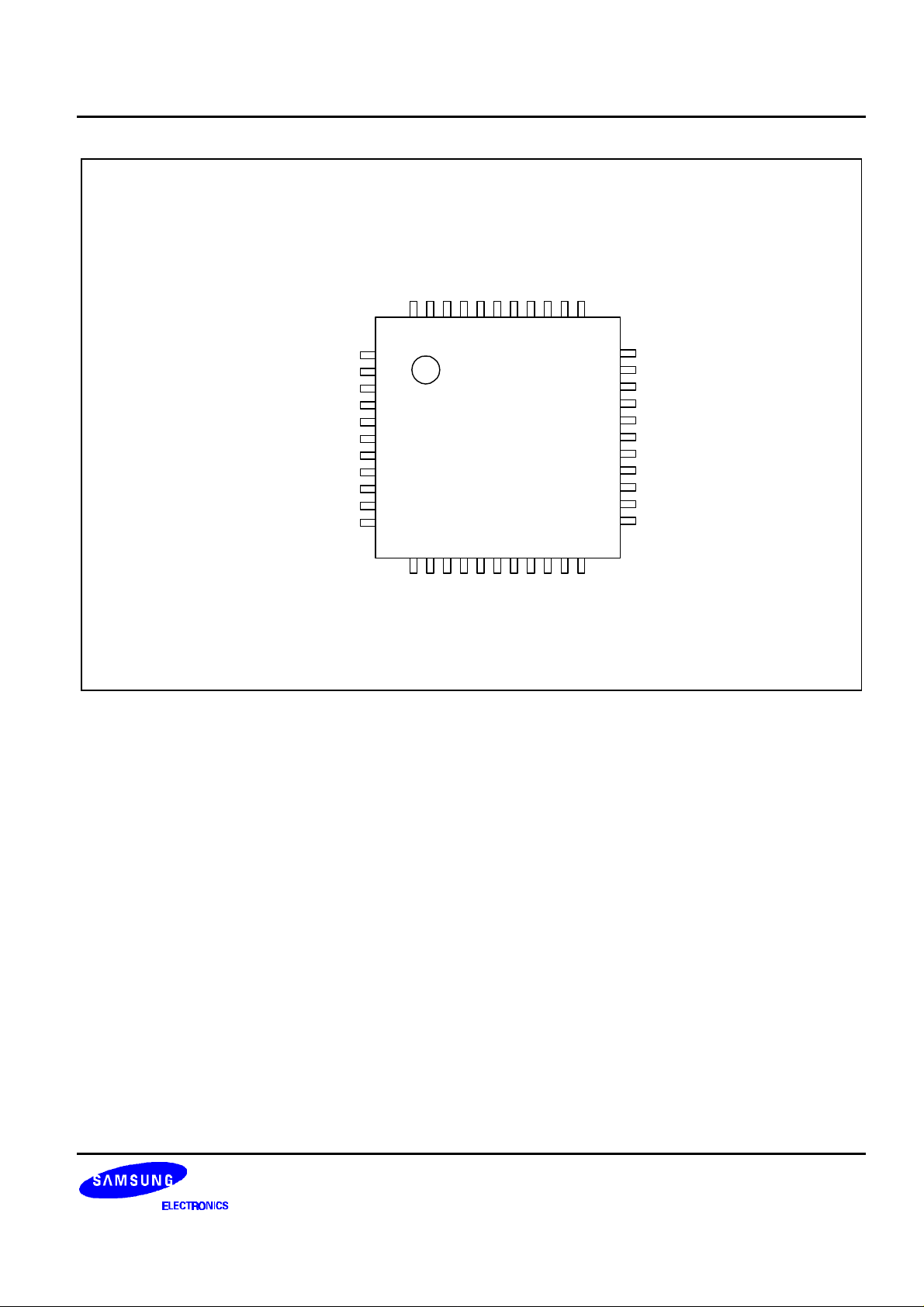
Figure 1-3. S3C7414 Pin Assignment (44-QFP)
4443424140393837363534
1
2
3
4
5
6
7
8
9
10
11
S3C7414
(44-QFP)
1213141516171819202122
P4.3
P5.0
P5.1
P5.2
P5.3
RESET
P0.0/SCK
P0.2/SI
P0.1/SO
P0.3/BUZ
NC
33
32
31
30
29
28
27
26
25
24
23
P7.2
P7.1
P7.0
P6.3/KS3
P6.2/KS2
P6.1/KS1
P6.0/KS0
P1.3/INT4
P1.2/INT2
P1.1/INT1
P1.0/INT0
1-6

S3C7414/P7414/C7424/P7424/C7434/P7434 PRODUCT OVERVIEW
VSS
XOUT
XIN
TEST
P4.1
P4.2
RESET
NC
P4.3
P5.0
P5.1
P5.2
P5.3
P0.0/SCK
P0.1/SO
1
2
3
4
5
6
7
8
9
10
11
12
13
14
15
S3C7424
(30-SDIP)
30
29
28
27
26
25
24
23
22
21
20
19
18
17
16
VDD
P4.0
P3.3/PWM/TCLO1
P3.2/CLO/TCL1
AVREF
NC
P2.3/AD3
P2.2/AD2
P2.1/AD1
P2.0/AD0
P1.2/INT2
P1.1/INT1
P1.0/INT0
P0.3/BUZ
P0.2/SI
Figure 1-4. S3C7424 Pin Assignment (30-SDIP)
VSS
XOUT
XIN
TEST
P4.1
P4.2
RESET
P4.3
P5.0
P5.1
P5.2
P5.3
P0.0/SCK
P0.1/SO
1
2
3
4
5
6
7
8
9
10
11
12
13
14
S3C7424
(28-SOP)
28
27
26
25
24
23
22
21
20
19
18
17
16
15
VDD
P4.0
P3.3/PWM/TCLO1
P3.2/CLO/TCL1
AVREF
P2.3/AD3
P2.2/AD2
P2.1/AD1
P2.0/AD0
P1.2/INT2
P1.1/INT1
P1.0/INT0
P0.3/BUZ
P0.2/SI
Figure 1-5. S3C7424 Pin Assignment (28-SOP)
1-7
PRODUCT OVERVIEW S3C7414/P7414/C7424/P7424/C7434/P7434
P2.0/AD0
P2.1/AD1
P2.2/AD2
P2.3/AD3
P3.0/AD4
P3.1/AD5
AVREF
P3.2/CLO/TCL1
P3.3/PWM/TCLO1
P4.0
VDD
VSS
XOUT
XIN
TEST
P4.1
P4.2
RESET
P4.3
P5.0
P5.1
Figure 1-6. S3C7434 Pin Assignment (42-SDIP)
1
2
3
4
5
6
7
8
9
10
11
12
13
14
15
16
17
18
19
20
21
S3C7434
(42-SDIP)
42
41
40
39
38
37
36
35
34
33
32
31
30
29
28
27
26
25
24
23
22
P8.2
P8.1/TCLO0
P8.0/TCL0
P7.3
P7.2
P7.1
P7.0
P6.3/KS3
P6.2/KS2
P6.1/KS1
P6.0/KS0
P1.3/INT4
P1.2/INT2
P1.1/INT1
P1.0/INT0
P0.3/BUZ
P0.2/SI
P0.1/SO
P0.0/SCK
P5.3
P5.2
1-8
S3C7414/P7414/C7424/P7424/C7434/P7434 PRODUCT OVERVIEW
NC
P3.1/AD5
P3.0/AD4
P2.3/AD3
P2.2/AD2
P2.1/AD1
P2.0/AD0
P8.2
P8.1/TCLO0
P8.0/TCL0
P7.3
AVREF
P3.2/CLO/TCL1
P3.3/PWM/TCLO1
P4.0
VDD
VSS
XOUT
XIN
TEST
P4.1
P4.2
Figure 1-7. S3C7434 Pin Assignment (44-QFP)
4443424140393837363534
1
2
3
4
5
6
7
8
9
10
11
S3C7434
(44-QFP)
1213141516171819202122
P4.3
P5.0
P5.1
P5.2
P5.3
RESET
P0.0/SCK
P0.2/SI
P0.1/SO
P0.3/BUZ
NC
33
32
31
30
29
28
27
26
25
24
23
P7.2
P7.1
P7.0
P6.3/KS3
P6.2/KS2
P6.1/KS1
P6.0/KS0
P1.3/INT4
P1.2/INT2
P1.1/INT1
P1.0/INT0
1-9
PRODUCT OVERVIEW S3C7414/P7414/C7424/P7424/C7434/P7434
PIN DESCRIPTIONS
Table 1-2. S3C7414/C7434 Pin Descriptions
Pin Name Pin Type Description Number Share Pin
P0.0
P0.1
P0.2
P0.3
P1.0
P1.1
P1.2
P1.3
P2.0
P2.1
P2.2
P2.3
P3.0
P3.1
P3.2
P3.3
P4.0
P4.1
P4.2
P4.3
P5.0–P5.3
P6.0–P6.3
P7.0–P7.3
P8.0
P8.1
P8.2
I/O 4-bit I/O port.
1-bit or 4-bit read/write and test is possible.
Individual pins are software configurable as input or
output.
24 (18)
25 (19)
26 (20)
27 (21)
4-bit pull-up resistors are software assignable; pull-up
resistors are automatically disabled for output pins.
I 4-bit input port.
1-bit and 4-bit read and test is possible.
3-bit pull-up resistors are individually assignable by
software to pins P1.0, P1.1, and P1.2.
I/O 4-bit I/O port.
N-channel open-drain output.
1-bit or 4-bit write and test is possible.
Individual pins are software configurable as AD input
28 (23)
29 (24)
30 (25)
31 (26)
1 (38)
2 (39)
3 (40)
4 (41)
or output.
4-bit pull-up resistors are software assignable; pull-up
resistors are automatically disabled for output pins.
I/O Same as Port 0 (P0.0–P0.3) 5 (42)
6 (43)
8 (2)
9 (3)
I/O 4-bit I/O ports.
Ports 4 and 5 can be configured individually as nchannel open-drain or as CMOS push-pull output by
software.
1-bit and 4-bit read/write and test is possible.
Ports 4 and 5 can be paired to enable 8-bit data
10 (4)
16 (10)
17 (11)
19 (13)
20–23
(14–17)
transfer.
4-bit pull-up resistors are software assignable; pull-up
resistors are automatically disabled for output pins.
I/O Same as Port 0 except port 8 is a 3-bit I/O port 32–35
(27–30)
36–39
(31–34)
40 (35)
41 (36)
42 (37)
SCK
SO
SI
BUZ
INT0
INT1
INT2
INT4
AD0
AD1
AD2
AD3
AD4
AD5
CLO/TCL1
PWM/TCLO1
–
KS0–KS3
–
TCL0
TCLO0
–
1-10

S3C7414/P7414/C7424/P7424/C7434/P7434 PRODUCT OVERVIEW
Table 1-2. S3C7414/C7434 Pin Descriptions (Continued)
Pin Name Pin Type Description Number Share Pin
SCK
I/O Serial I/O interface clock signal 24 (18) P0.0
SO I/O Serial data output 25 (19) P0.1
SI I/O Serial data input 26 (20) P0.2
BUZ I/O 2 kHz, 4kHz, 8kHz, or 16 kHz frequency output at the
27 (21) P0.3
watch timer clock frequency of 32.768 kHz
INT0, INT1 I External interrupts. The triggering edge for INT0 and
INT1 is selectable. Only INT0 is synchronized with the
28–29
(23–24)
P1.0, P1.1
system clock.
INT2 I Quasi-interrupt input with rising edge detection 30 (25) P1.2
INT4 I External interrupts with detection of rising and falling
31 (26) P1.3
edges
AD0–AD3
I/O A/D converter analog inputs 1–4
P2.0–P2.3
(38–41)
AD4–AD5
5–6
P3.0–P3.1
(42–43)
TCL0 I/O External clock input for timer/counter0 40 (35) P8.0
TCLO0 I/O Timer/counter clock output 41 (36) P8.1
CLO I/O Clock output 8 (2) P3.2
TCL1 I/O External clock input for timer/counter1 8 (2) P3.2
PWM I/O PWM output 9 (3) P3.3
TCLO1 I/O Timer/counter clock output1 9 (3) P3.3
KS0–KS3 I/O Quasi-interrupt input with falling edge detection 32–35
P6.0–P6.3
(27–30)
V
DD
V
SS
RESET
XIN, X
out
AV
REF
TEST I
– Main power supply 11 (5) –
– Ground 12 (6) –
I Reset signal 18 (12) –
– Crystal, ceramic, or RC oscillator signal for system
clock.
14, 13
(8, 7)
– A/D converter analog reference voltage 7 (1) –
Test signal input (must be connected to V
SS
)
15 (9) –
–
NC – No connection (no bonding pin) (22, 44) –
NOTE: Parentheses indicate 44-QFP pin number.
1-11

PRODUCT OVERVIEW S3C7414/P7414/C7424/P7424/C7434/P7434
Table 1-3. S3C7424 Pin Descriptions
Pin Name Pin Type Description Number Share Pin
P0.0
P0.1
P0.2
P0.3
P1.0
P1.1
P1.2
P2.0
P2.1
P2.2
P2.3
P3.2
P3.3
P4.0
P4.1
P4.2
P4.3
P5.0–P5.3
I/O 4-bit I/O port.
1-bit or 4-bit read/write and test is possible.
Individual pins are software configurable as input or
output.
14 (13)
15 (14)
16 (15)
17 (16)
4-bit pull-up resistors are software assignable; pull-up
resistors are automatically disabled for output pins.
I 4-bit input port.
1-bit and 4-bit read and test is possible.
3-bit pull-up resistors are individually assignable by
18 (17)
19 (18)
20 (19)
software to pins P1.0, P1.1, and P1.2.
I/O 4-bit I/O port.
N-channel open-drain output.
1-bit or 4-bit write and test is possible.
Individual pins are software configurable as AD input
21 (20)
22 (21)
23 (22)
24 (23)
or output.
4-bit pull-up resistors are software assignable; pull-up
resistors are automatically disabled for output pins.
I/O Same as Port 0 (P0.0–P0.3) 27 (25)
28 (26)
I/O 4-bit I/O ports.
Ports 4 and 5 can be configured individually as nchannel open-drain or as CMOS push-pull output by
software.
29 (27)
5 (5)
6 (6)
9 (8)
1-bit and 4-bit read/write and test is possible.
Ports 4 and 5 can be paired to enable 8-bit data
transfer.
10–13
(9–12)
4-bit pull-up resistors are software assignable; pull-up
resistors are automatically disabled for output pins.
SCK
SO
SI
BUZ
INT0
INT1
INT2
AD0
AD1
AD2
AD3
CLO/TCL1
PWM/TCLO1
–
1-12
S3C7414/P7414/C7424/P7424/C7434/P7434 PRODUCT OVERVIEW
Table 1-3. S3C7424 Pin Descriptions (Continued)
Pin Name Pin Type Description Number Share Pin
SCK
I/O Serial I/O interface clock signal 14 (13) P0.0
SO I/O Serial data output 15 (14) P0.1
SI I/O Serial data input 16 (15) P0.2
BUZ I/O 2 kHz, 4kHz, 8kHz, or 16 kHz frequency output at the
17 (16) P0.3
watch timer clock frequency of 32.768 kHz
INT0, INT1 I External interrupts. The triggering edge for INT0 and
INT1 is selectable. Only INT0 is synchronized with the
18, 19
(17, 18)
P1.0, P1.1
system clock.
INT2 I Quasi-interrupt input with rising edge detection 20 (19) P1.2
AD0–AD3 I/O A/D converter analog inputs 21–24
P2.0–P2.3
(20–23)
CLO I/O Clock output 27 (25) P3.2
TCL1 I/O External clock input for timer/counter1 27 (25) P3.2
PWM I/O PWM output 28 (26) P3.3
TCLO1 I/O Timer/counter clock output1 28 (26) P3.3
V
DD
V
SS
RESET
XIN, X
OUT
AV
REF
TEST I
– Main power supply 30 (28) –
– Ground 1 (1) –
I Reset signal 7 (7) –
– Crystal, ceramic, or RC oscillator signal for system
clock.
3, 2
(3, 2)
– Internal A/D converter analog reference voltage 26 (24) –
Test signal input (must be connected to V
SS
)
4 (4) –
–
NC – No connection (no bonding pin) 8, 25 –
NOTE: Parentheses indicate 28-SOP pin number.
1-13
PRODUCT OVERVIEW S3C7414/P7414/C7424/P7424/C7434/P7434
Table 1-4. Overview of S3C7414/C7424/C7434Pin Data
Pin Names Share Pins I/O Type Reset Value Circuit Type
P0.0–P0.3
P1.0
P1.1
P1.2
SCK, SO, SI, BUZ
(note)
INT0
(note)
INT1
(note)
INT2
I/O Input Type D
I Input Type A-1
P1.3 INT4 I Input Type A
P2.0–P2.3 AD0–AD3 I/O AD input Type F-3
P3.0
P3.1
P3.2
P3.3
P4.0–P4.3
AD4
I/O Input Type F
AD5
CLO/TCL1
TCLO1/PWM
– I/O Input Type E
Type F
Type D
Type D
P5.0–P5.3
P6.0
P6.1
P6.2
P6.3
KS0
KS1
KS2
KS3
(note)
(note)
(note)
(note)
P7.0–P7.3 –
(note)
P8.0
P8.1
P8.2
VDD, V
XIN, X
RESET
AV
REF
SS
OUT
TCL0
TCLO0
–
– – – –
– – – –
–
– –
TEST – I –
I/O
I/O
I/O
I –
Input
Input
Input
Type B-2
– –
Type D
Type D
Type D
(note)
–
NC – – – –
NOTE: A noise filter circuit is built-in.
1-14
S3C7414/P7414/C7424/P7424/C7434/P7434 PRODUCT OVERVIEW
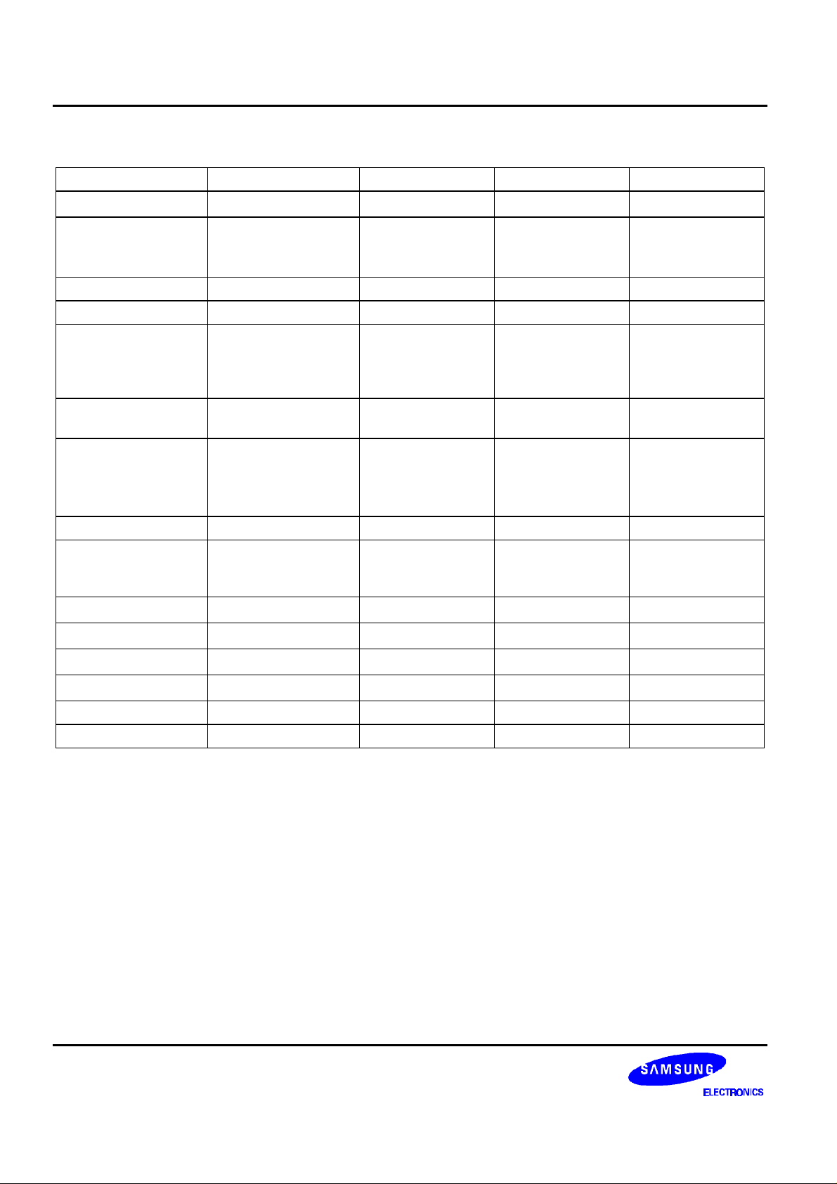
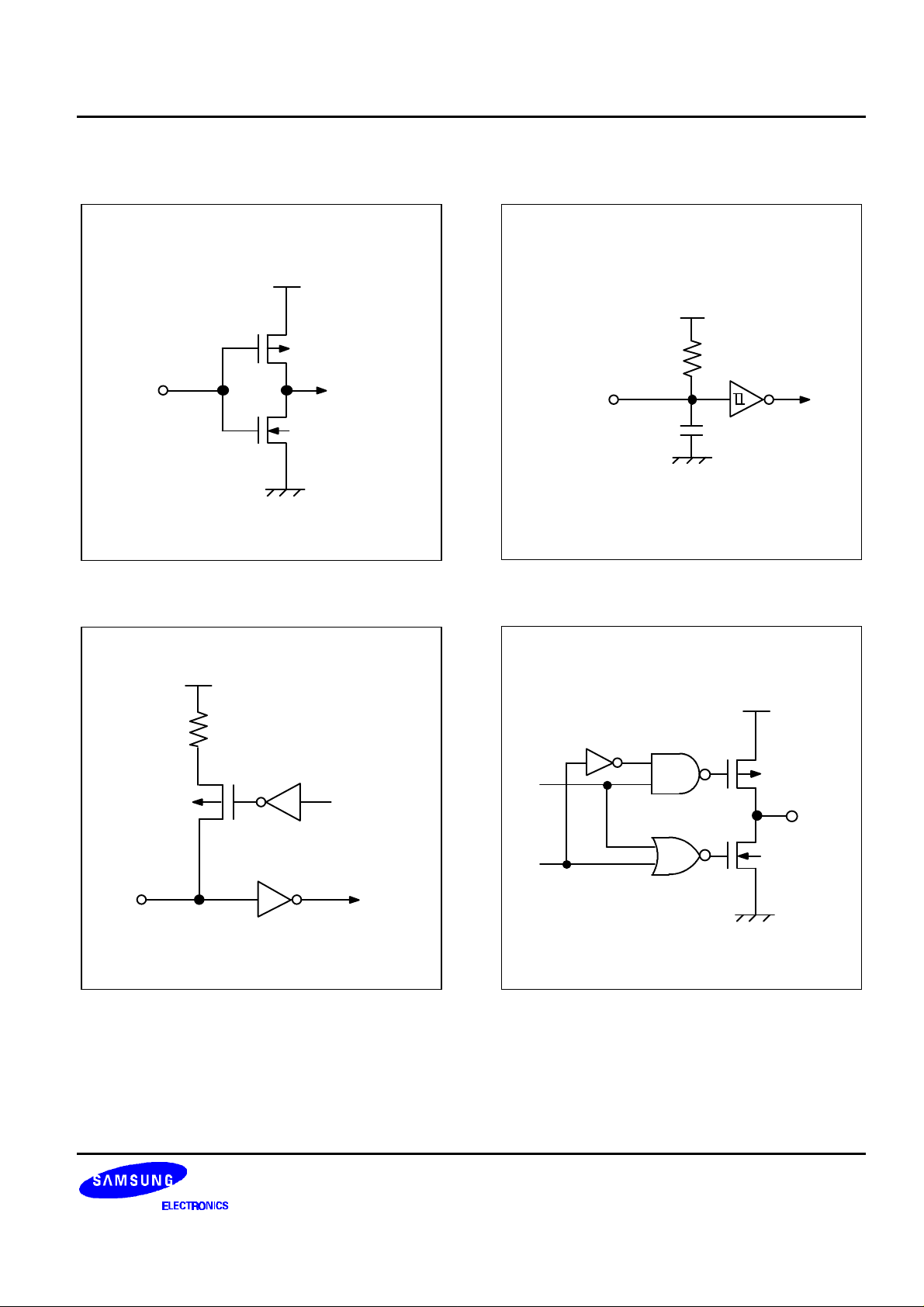
PIN CIRCUIT DIAGRAMS
V
DD
V
DD
P-CHANNEL
IN
N-CHANNEL
Figure 1-8. Pin Circuit Type A
V
DD
PULL-UP
RESISTOR
ENABLE
DATA
1M
Ω
RESET
7pF
Figure 1-10. Pin Circuit Type B-2
V
DD
P-CHANNEL
OUT
IN
CIRCUIT TYPE A
Figure 1-9. Pin Circuit Type A-1
N-CHANNEL
OUTPUT
DISABLE
Figure 1-11. Pin Circuit Type C
1-15
 Loading...