

Samsung S3C72E8, S3P72E8 Datasheet

S3C72E8/P72E8 PRODUCT OVERVIEW
1 PRODUCT OVERVIEW
OVERVIEW
The S3C72E8/P72E8 is a SAM47 core-based 4-bit CMOS single-chip microcontroller. It has a timer/counter and
LCD drivers.
The S3P72E8 is especially suited for use in data bank, telephone and LCD general purpose.
It is built around the SAM47 core CPU and contains ROM, RAM, 39 I/O lines, programmable timer/counter,
buzzer output, enough LCD dot matrix, and segment drive pins.
The S3C72E8/P72E8 can be used for dedicated control functions in a variety of applications, and is especially
designed for multi data bank, telephone and LCD game.
OTP
The S3C72E8 microcontroller is also available in OTP (One Time Programmable) version, S3P72E8. S3P72E8
microcontroller has an on-chip 8 K-byte one-time-programable EPROM instead of masked ROM. The S3P72E8
is comparable to S3C72E8, both in function and in pin configuration.
1-1

PRODUCT OVERVIEW S3C72E8/P72E8
FEATURES SUMMARY
Memory
• 8192 × 8 bit program memory
• 5120 × 4 bit data memory in S3C72E8
• 108 x 5 bit display memory
39 I/O Pins
• Input: 6 pins
• I/O: 17 pins
• Output: maximum 16 pins for 1-bit level output
(sharing with segment driver outputs)
8-Bit Basic Timer
• Four internal timer functions
8-Bit Timer/Counter 0
• Programmable 8-bit timer
• External event counter
• Arbitrary clock frequency output
• External clock signal divider
Watch Timer
• Time interval generation: 0,5ms, 3,9ms at
32768Hz
• 4 frequency (2/4/8/16 kHz) outputs to BUZ pin
Interrupts
• Three external vectored interrupts: INT0, INT1,
INTP0
• Two internal vectored interrupts: INTB, INTT0
• Two quasi-interrupts: INTW, INT2
LCD Display
• 12 characters dot matrix display (5 x 7)
• 12 digit display (8 segments)
• 60 segments and 9 common pins
Power-Down Modes
• Idle mode (only CPU clock stops)
• Stop mode (Main-System clock and CPU clock
stops)
Oscillation Sources
• Crystal, ceramic, or External RC for system clock
• Main-system clock frequency: 0.4 MHz - 6MHz
• Sub-system clock frequency: 32,768kHz
• CPU clock divider circuit (by 4,8, or 64)
Instruction Execution Times
• 0.67, 1.33, 10.7 µs at 6MHz
• 0.95, 1.91, 15.3 µs at 4.19 MHz
• 122 µs at 32.768 kHz
Operating Temperature
• -45 °C to 85 °C
Operating Voltage Range
• 1.8 V to 5.5 V
Package Type
• 100-pin QFP Package
Memory Mapped I/O Structure
1-2

S3C72E8/P72E8 PRODUCT OVERVIEW
BLOCK DIAGRAM
XOUT
XIN
INTT0, INTB, INTW
INT0, INT1, INTP0, INT2
8-Bit
Timer/
Counter 0
RESET
Interrupt
Control
Block
XTIN
XTOUT
Clock
Instruction
Register
Input Port 0
Input Port 1
P0.0-P0.3/
K0-K3
P1.0/INT0
P1.1/INT1
COM0-COM8
SEG16-SEG59
SEG0-SEG15
/P8.0-P8.15
Watch Timer
Basic Timer
LCD
Driver/
Controller
Figure 1-1. S3C72E8/P72E8 Specified Block Diagram
Internal
Interrupts
Instruction Decoder
Arithmetic
and
Logic Unit
Data and
Display
Memory
Program
Counter
Program
Status Word
Stack
Pointer
8 K Byte
Program
Memory
I/O Port 2
I/O Port 4
I/O Port 5
I/O Port 6
I/O Port 7
Output Port 8
P2.0/BUZ
P2.1/CLO
P4.0/TCL0
P4.1/TCLO0
P4.2
P5.0-P5.3
P6.0-P6.3/
KS0-KS3
P7.0-P7.3/
KS4-KS7
P8.0-P8.15/
SEG0-SEG15
1-3

PRODUCT OVERVIEW S3C72E8/P72E8
PIN ASSIGNMENTS
SEG39
SEG40
SEG41
SEG42
SEG43
SEG44
SEG45
SEG46
SEG47
SEG48
SEG49
SEG50
SEG51
SEG52
SEG53
SEG54
SEG55
SEG56
SEG57
SEG58
81
82
83
84
85
86
87
88
89
90
91
92
93
94
95
96
97
98
99
100
P6.0/KS0
P6.1/KS1
P6.2/KS2
P6.3/KS3
P7.0/KS4
P7.1/KS5
P7.2/KS6
P7.3/KS7
P2.0/BUZ
P2.1/CLO
TCL0/P4.0
TCLO0/P4.1
SEG59
COM4
COM5
COM6
COM7
COM8
VDD
V
Xout
Xin
TEST
XTin
XTout
RESET
P5.0
P5.1
P5.2
P5.3
SS
1
2
3
4
5
6
7
8
9
10
11
12
13
14
15
16
17
18
19
20
21
22
23
24
25
26
27
28
29
30
31
32
33
34
35
S3C72E8
100-QFP 1420C
41
40
39
38
37
36
42
43
44
45
46
47
48
49
50
80
79
78
77
76
75
74
73
72
71
70
69
68
67
66
65
64
63
62
61
60
59
58
57
56
55
54
53
52
51
SEG38
SEG37
SEG36
SEG35
SEG34
SEG33
SEG32
SEG31
SEG30
SEG29
SEG28
SEG27
SEG26
SEG25
SEG24
SEG23
SEG22
SEG21
SEG20
SEG19
SEG18
SEG17
SEG16
SEG15/P8.15
SEG14/P8.14
SEG13/P8.13
SEG12/P8.12
SEG11/P8.11
SEG10/P8.10
SEG9/P8.9
1-4
SEG8/P8.8
SEG7/P8.7
SEG6/P8.6
SEG5/P8.5
SEG4/P8.4
SEG3/P8.3
SEG2/P8.2
SEG1/P8.1
SEG0/P8.0
COM3
COM2
COM1
COM0
INT0/P1.0
INT1/P1.1
P0.0/K0
P0.1/K1
P0.2/K2
P0.3/K3
P4.2
Figure 1-2. S3C72E8 Pin Assignment Diagram
S3C72E8/P72E8 PRODUCT OVERVIEW
PIN DESCRIPTIONS
Table 1-1. Pin Descriptions
Pin Name Pin
P0.0 - P0.3
Type
I
4-bit input port.
Description Circuit
Type
A-1 35-32
Pin
Number
Share Pin
K0-K3
1 and 4-bit read, and test are possible.
Pull-up registers.
P1.0
P1.1
2-bit Input port.
I
1 and 4-bit read, and test are possible, 2-bit pull-up
A-3 37
36
INT0
INT1
resistors are assignable by software.
P2.0
P2.1
2-bit I/O port. 1 and 4-bit read/write, and test are
I/O
possible.
D 23
24
BUZ
CLO
Each individual pin can be specified as input or
output.
2-bit pull-up resistors are assignable by software.
Pull-up resistors are automatically disabled for
output pins.
P4.0
P4.1
P4.2
P5.0 - P5.3
4-bit I/O port. 1, 4, and 8-bit read/write, and test are
I/O
possible.
4-pin unit can be specified as input or output.
4-bit pull-up resistors are assignable by software.
E
E-1
E-1
E-1
29
30
31
25-28
TCL0
TCLO0
Pull-up resistors are automatically disabled for
output pins.
Individual pins are software configurable as opendrain or push-pull output.
P6.0 - P6.3
4-bit I/O port. 1, 4,and 8-bit read/write, and test are
I/O
D-1 7-10 KS0 - KS3
possible.
Each individual pin can be specified as input or
output.
4-bit pull-up resistors are assignable by software.
Pull-up resistors are automatically disabled for
output pins.
P7.0 - P7.3 4-bit I/O port. 1, 4, and 8-bit read/write, and test are
11-14 KS4 - KS7
possible.
4-pin unit can be specified as input or output.
4-bit pull-up resistors are assignable by software.
Pull-up resistors are automatically disabled for
output pins.
P8.0 - P8.15 O 4-bit controllable output.
(Dual function as segment output pins)
SEG16-SEG59 LCD segment display signal output. H-10 58-100
H-9 42-57 SEG0 -
SEG15
-
,1
SEG0 - SEG15 LCD segment display signal output. H-9 42-57 P8.0 - P8.15
COM0 - COM8 LCD common signal output. H-11 38-41
-
2-6
INT0 - INT1 I External interrupts. The triggering edge for INT0,
37-36 P1.0 -P1.1
and INT1 is selectable
KS0 - KS7 I/O Quasi-interrupt input for falling edge detection. 7-14 P6.0 - P7.3
K0 - K3 I Vector interrupt input
35-32 P0.0 - P0.3
K0 - K3: falling edge detection
1-5
PRODUCT OVERVIEW S3C72E8/P72E8
Table 1-1. Pin Descriptions (Continued)
Pin Name Pin
Type
BUZ I/O 2,4,8 kHz or 16kHz frequency output for buzzer
Description Circuit
Type
- 23 P2.0
Pin
Num.
Share Pin
signal.
CLO Clock output - 24 P2.1
Xin, X
out
- Crystal, ceramic or RC oscillator pins for main
- 18, 17 -
system clock.
XTin, XT
out
- Crystal oscillator pins for sub-system clock. - 20, 21 TCL0 I/O External clock input for Timer/Counter 0 - 29 P4.0
TCLO0 I/O Timer/Counter 0 clock output - 30 P4.1
RESET
V
DD
V
SS
TEST I Test input: it must be connected to V
I Reset input (active low). B 22 -
- Power supply. - 15 -
- Ground. - 16 -
SS
- 19 -
1-6

S3C72E8/P72E8 PRODUCT OVERVIEW
PIN CIRCUIT DIAGRAMS
V
V
DD
Pull-up
Resistor
DD
P-channel
IN
N-channel
Vss
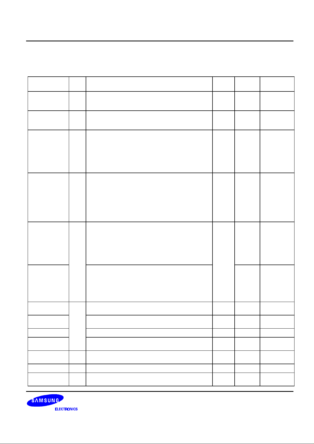
Figure 1-3. Pin Circuit Type A
V
DD
Pull-up
Pull-up
Resistor
Enable
P-channel
IN
Schmitt Trigger
Figure 1-5. Pin Circuit Type A-3
V
DD
Pull-up
Register
Pull-up
Resistor
Enable
IN
Figure 1-4. Pin Circuit Type A-1
P-channel
IN
Schmitt Trigger
Figure 1-6. Pin Circuit Type B
1-7
PRODUCT OVERVIEW S3C72E8/P72E8
V
DD
V
DD
Pull-up
Resistor
Pull-up
Resistor
Enable
P-channel
Data
P-channel
Output
Disable
Pull-Up
Resistor
Enable
Data
Output
Disable
V
SS
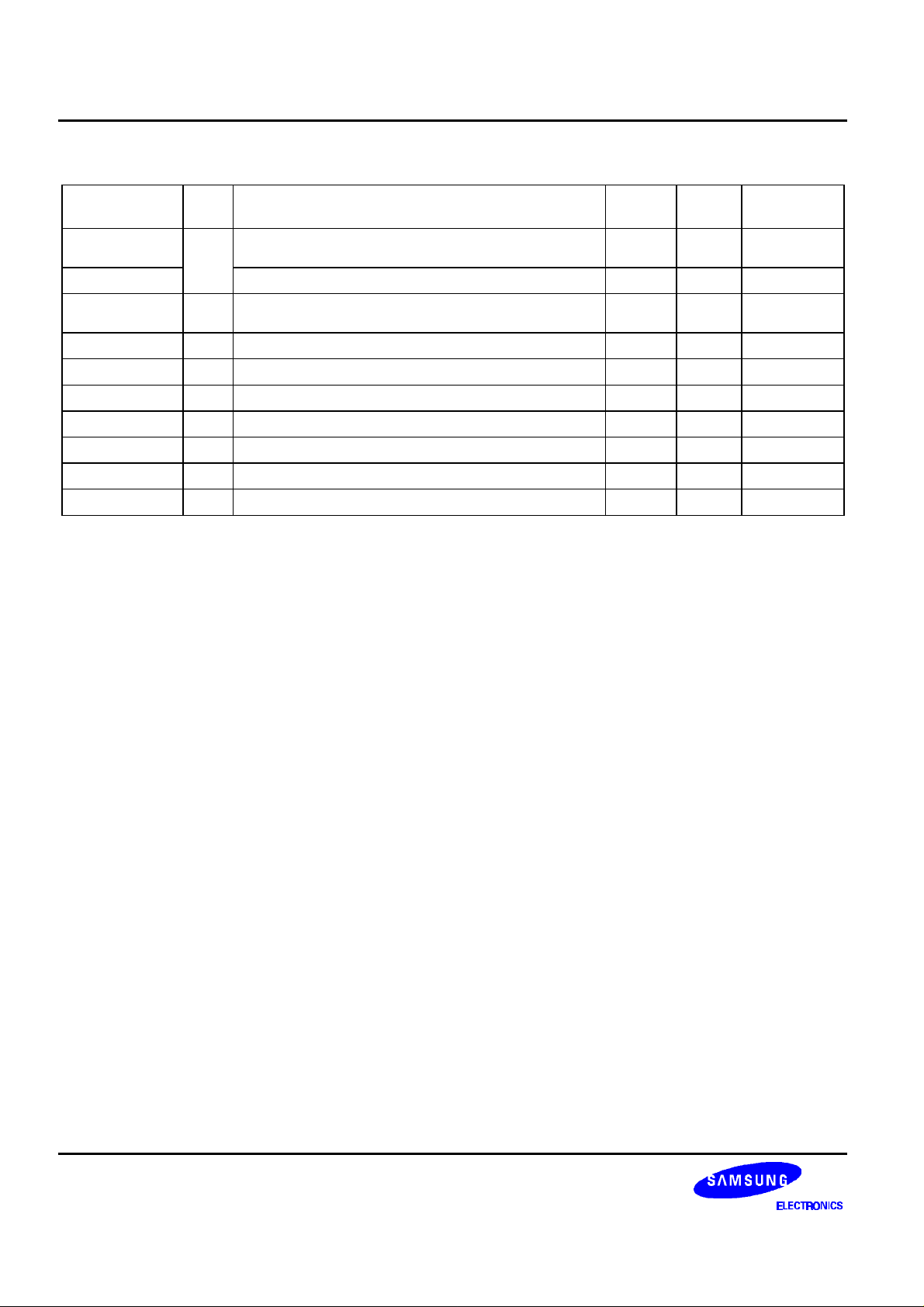
Figure 1-7. Pin Circuit Type C
V
DD
Pull-Up
Resistor
P-channel
Type C
OUT
N-channel
In/Out
Data
Output
Disable
Type C
Schmitt Trigger
Figure 1-9. Pin Circuit Type D-1
VDD
PNE
Data
Output
Disable
VDD
P-channel
N-channel
IN/OUT
Pull-up
Resistor
Pull-up
Resistor
Enable
I/O
1-8
Figure 1-8. Pin Circuit Type D
Schmitt Trigger
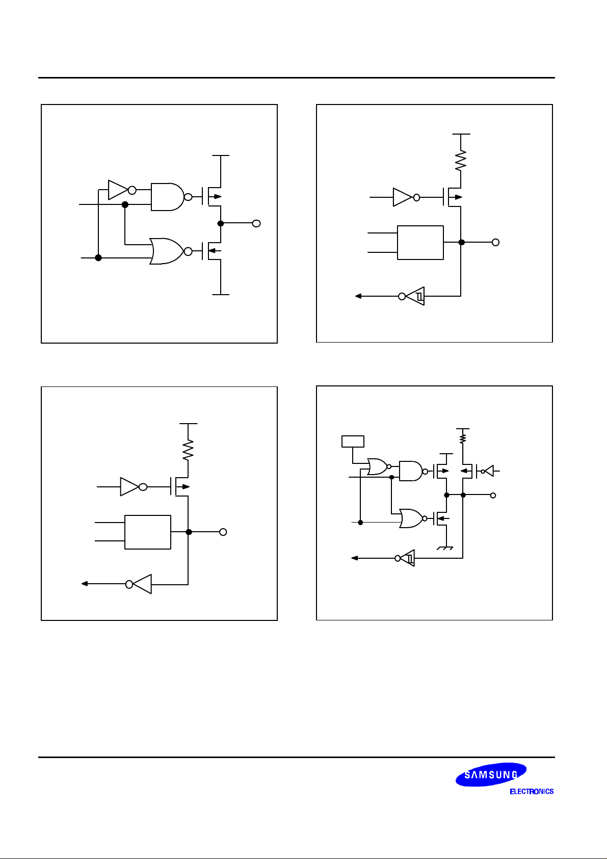
Figure 1-10. Pin Circuit Type E
S3C72E8/P72E8 PRODUCT OVERVIEW
V
DD
PNE
V
DD
Pull-up
resistor
Pull-up
V
LC2
Resistor
Data
P-channel
I/O
Enable
Segment
Data
OUT
Output
Disable
N-channel
Figure 1-11. Pin Circuit Type E-1
SEG Data/P8.0-P8.15
V
LC2
V
LC0
Key
strobe
Vss
OUT
V
LC0
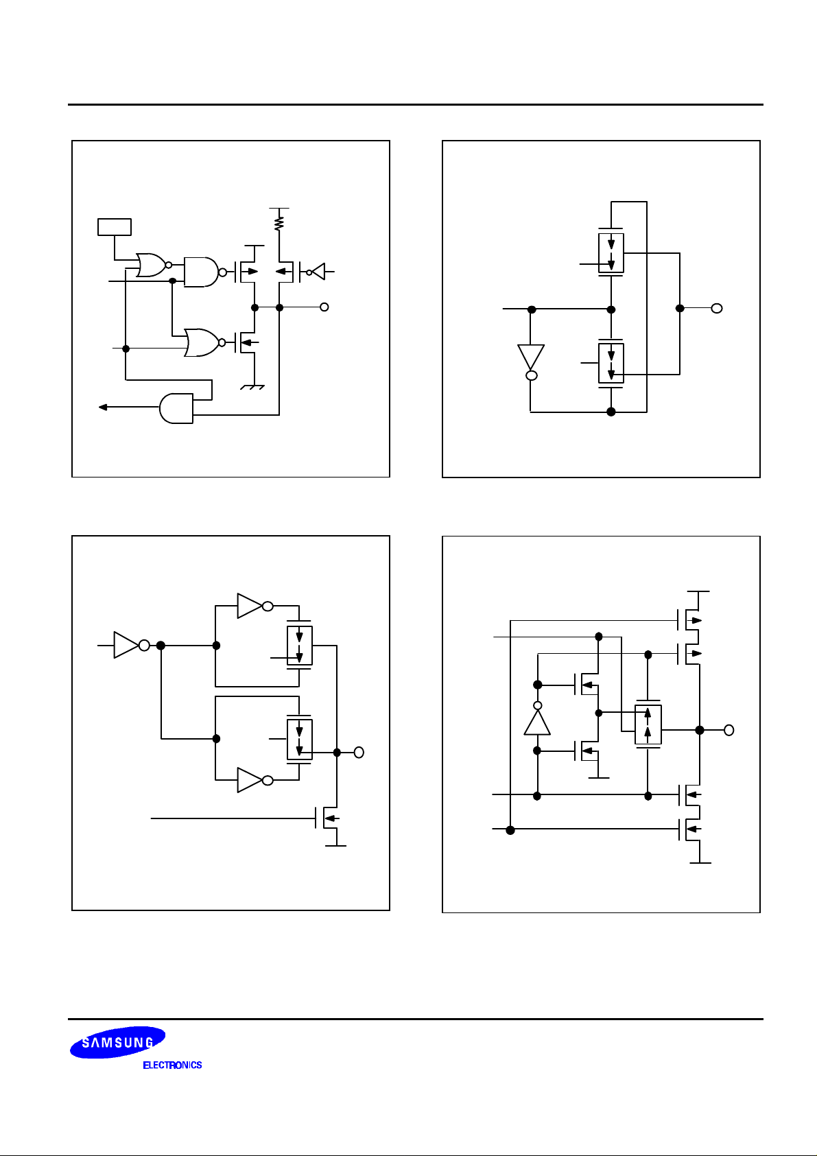
Figure 1-13. Pin Circuit Type H-10
V
LC1
COM
Data
Polarity
Vss
V
Vss
DD
OUT
Figure 1-12. Pin Circuit Type H-9
Figure 1-14. Pin Circuit Type H-11
1-9
 Loading...