

Samsung M391B5273DH0, M391B5773DH0 User Manual
Rev. 1.0, Sep. 2010
240pin Unbuffered DIMM
1.35V
based on 2Gb D-die
78FBGA with Lead-Free & Halogen-Free
(RoHS compliant)
M391B5773DH0
M391B5273DH0
datasheet
SAMSUNG ELECTRONICS RESERVES THE RIGHT TO CHANGE PRODUCTS, INFORMATION AND
SPECIFICATIONS WITHOUT NOTICE.
Products and specifications discussed herein are for reference purposes only. All information discussed
herein is provided on an "AS IS" basis, without warranties of any kind.
This document and all information discussed herein remain the sole and exclusive property of Samsung
Electronics. No license of any patent, copyright, mask work, trademark or any other intellectual property
right is granted by one party to the other party under this document, by implication, estoppel or otherwise.
Samsung products are not intended for use in life support, critical care, medical, safety equipment, or
similar applications where product failure could result in loss of life or personal or physical harm, or any
military or defense application, or any governmental procurement to which special terms or provisions
may apply.
For updates or additional information about Samsung products, contact your nearest Samsung office.
All brand names, trademarks and registered trademarks belong to their respective owners.
ⓒ 2010 Samsung Electronics Co., Ltd. All rights reserved.
- 1 -
Rev. 1.0
Unbuffered DIMM
datasheet DDR3L SDRAM
Revision History
Revision No. History Draft Date Remark Editor
1.0 - First Release Sep. 2010 - S.H.Kim
- 2 -

Rev. 1.0
Unbuffered DIMM
datasheet DDR3L SDRAM
Table Of Contents
240pin Unbuffered DIMM based on 2Gb D-die
1. DDR3L Unbuffered DIMM Ordering Information........................................................................................................... 4
2. Key Features................................................................................................................................................................. 4
3. Address Configuration ..................................................................................................................................................4
4. x72 DIMM Pin Configurations (Front side/Back side) ................................................................................................... 5
5. Pin Description ............................................................................................................................................................. 6
6. SPD and Thermal Sensor for ECC UDIMMs ................................................................................................................ 6
7. Input/Output Functional Description..............................................................................................................................7
7.1 Address Mirroring Feature....................................................................................................................................... 8
7.1.1. DRAM Pin Wiring Mirroring.............................................................................................................................. 8
8. Function Block Diagram:...............................................................................................................................................9
8.1 2GB, 256Mx72 ECC Module (Populated as 1 rank of x8 DDR3 SDRAMs) ............................................................ 9
8.2 4GB, 512Mx72 ECC Module (Populated as 2 ranks of x8 DDR3 SDRAMs)........................................................... 10
9. Absolute Maximum Ratings ..........................................................................................................................................11
9.1 Absolute Maximum DC Ratings............................................................................................................................... 11
9.2 DRAM Component Operating Temperature Range ................................................................................................ 11
10. AC & DC Operating Conditions...................................................................................................................................11
10.1 Recommended DC Operating Conditions (SSTL-15)............................................................................................11
11. AC & DC Input Measurement Levels ..........................................................................................................................12
11.1 AC & DC Logic Input Levels for Single-ended Signals.......................................................................................... 12
11.2 V
11.3 AC and DC Logic Input Levels for Differential Signals .......................................................................................... 15
11.3.1. Differential Signals Definition ......................................................................................................................... 15
11.3.2. Differential Swing Requirement for Clock (CK - CK
11.3.3. Single-ended Requirements for Differential Signals ...................................................................................... 17
11.3.4. Differential Input Cross Point Voltage ............................................................................................................ 18
11.4 Slew Rate Definition for Single Ended Input Signals .............................................................................................19
11.5 Slew rate definition for Differential Input Signals ................................................................................................... 19
12. AC & DC Output Measurement Levels ....................................................................................................................... 19
12.1 Single Ended AC and DC Output Levels............................................................................................................... 19
12.2 Differential AC and DC Output Levels ................................................................................................................... 19
12.3 Single-ended Output Slew Rate ............................................................................................................................ 20
12.4 Differential Output Slew Rate ................................................................................................................................ 21
13. IDD specification definition..........................................................................................................................................22
14. IDD SPEC Table .........................................................................................................................................................24
15. Input/Output Capacitance ...........................................................................................................................................25
16. Electrical Characteristics and AC timing .....................................................................................................................26
16.1 Refresh Parameters by Device Density................................................................................................................. 26
16.2 Speed Bins and CL, tRCD, tRP, tRC and tRAS for Corresponding Bin ................................................................ 26
16.3 Speed Bins and CL, tRCD, tRP, tRC and tRAS for corresponding Bin ................................................................. 26
16.3.1. Speed Bin Table Notes .................................................................................................................................. 28
17. Timing Parameters by Speed Grade ..........................................................................................................................30
17.1 Jitter Notes ............................................................................................................................................................ 33
17.2 Timing Parameter Notes........................................................................................................................................ 34
18. Physical Dimensions................................................................................................................................................... 35
18.1 256Mbx8 based 256Mx72 Module (1 Rank) - M391B5773DH0 ............................................................................ 35
18.2 256Mbx8 based 512Mx72 Module (2 Ranks) - M391B5273DH0 .......................................................................... 36
Tolerances.................................................................................................................................................... 14
REF
) and Strobe (DQS - DQS) ............................................. 15
- 3 -
Rev. 1.0
Unbuffered DIMM
datasheet DDR3L SDRAM
1. DDR3L Unbuffered DIMM Ordering Information
Part Number
M391B5773DH0-YF8/H9/K0 2GB 256Mx64 256Mx8(K4B2G0846D-HY##)*9 1 30mm
M391B5273DH0-YF8/H9/K0 4GB 512Mx72 256Mx8(K4B2G0846D-HY##)*18 2 30mm
NOTE :
1. "##" - F8/H9/K0
2. F8 - 1066Mbps 7-7-7 / H9 - 1333Mbps 9-9-9 / K0 - 1600Mbps 11-11-11
- DDR3-1600(11-11-11) is backward compatible to DDR3-1333(9-9-9), DDR3-1066(7-7-7)
- DDR3-1333(9-9-9) is backward compatible to DDR3-1066(7-7-7)
2
Density Organization Component Composition
Number of
Rank
2. Key Features
Speed
tCK(min) 2.5 1.875 1.5 1.25 ns
CAS Latency 6 7 9 11 n CK
tRCD(min) 15 13.125 13.5 13.75 ns
tRP(min) 15 13.125 13.5 13.75 ns
tRAS(min) 37.5 37.5 36 35 ns
tRC(min) 52.5 50.625 49.5 48.75 ns
DDR3-800 DDR3-1066 DDR3-1333 DDR3-1600
6-6-6 7-7-7 9-9-9 11-11- 11
Height
Unit
• JEDEC standard 1.35V(1.28V~1.45V) & 1.5V(1.425V~1.575V) Power Supply
•V
= 1.35V(1.28V~1.45V) & 1.5V(1.425V~1.575V)
DDQ
• 400MHz fCK for 800Mb/sec/pin, 533MHz fCK for 1066Mb/sec/pin, 667MHz fCK for 1333Mb/sec/pin, 800MHz fCK for 1600Mb/sec/pin
• 8 independent internal bank
• Programmable CAS Latency: 6,7,8,9,10,11
• Programmable Additive Latency(Posted CAS) : 0, CL - 2, or CL - 1 clock
• Programmable CAS Write Latency(CWL) = 5 (DDR3-800), 6 (DDR3-1066), 7 (DDR3-1333) and 8 (DDR3-1600)
• Burst Length: 8 (Interleave without any limit, sequential with starting address “000” only), 4 with tCCD = 4 which does not allow seamless read or
write [either On the fly using A12 or MRS]
• Bi-directional Differential Data Strobe
• On Die Termination using ODT pin
• Average Refresh Period 7.8us at lower then T
• Asynchronous Reset
85°C, 3.9us at 85°C < T
CASE
CASE
≤ 95°C
3. Address Configuration
Organization Row Address Column Address Bank Address Auto Precharge
256Mx8(2Gb) based Module A0-A14 A0-A9 BA0-BA2 A10/AP
- 4 -
Rev. 1.0
Unbuffered DIMM
datasheet DDR3L SDRAM
4. x72 DIMM Pin Configurations (Front side/Back side)
Pin Front Pin Back Pin Front Pin Back Pin Front Pin Back
1
2
V
REFDQ
121
V
SS
122 DQ4 43 NC 163
3 DQ0 123 DQ5 44
4 DQ1 124
5
6DQS
V
SS
125 DM0 46 CB3 166
0 126 NC 47
7 DQS0 127
8
V
SS
128 DQ6 KEY 89
9 DQ2 129 DQ7 49 NC 169
10 DQ3 130
11
V
SS
131 DQ12 51
12 DQ8 132 DQ13 52 BA2 172 A14 93 DQS
13 DQ9 133
14
15 DQS
V
SS
134 DM1 54
1 135 NC 55 A11 175 A9 96 DQ42 216 DQ47
16 DQS1 136
17
V
SS
137 DQ14 57
18 DQ10 138 DQ15 58 A5 178 A6 99 DQ48 219 DQ53
19 DQ11 139
20
V
SS
140 DQ20 60
21 DQ16 141 DQ21 61 A2 181 A1 102 DQS
22 DQ17 142
23
24 DQS
V
SS
143 DM2 63
2 144 NC 64
25 DQS2 145
26
V
SS
146 DQ22 66
27 DQ18 147 DQ23 67
28 DQ19 148
29
V
SS
149 DQ28 69
30 DQ24 150 DQ29 70 A10/AP 190 BA1 111 DQS
31 DQ25 151
32
33 DQS
V
SS
152 DM3 72
3 153 NC 73 WE 193 S0 114 DQ58 234 DQ63
34 DQS3 154
35
V
SS
155 DQ30 75
36 DQ26 156 DQ31 76
37 DQ27 157
38
V
SS
158 CB4 78
39 CB0 159 CB5 79 NC 199
40 CB1 160
41
V
SS
161 DM8 81 DQ32 201 DQ37
NOTE :
NC = No Connect; NU = Not Used; RFU = Reserved Future Use
, ODT1, CKE1: Used for dual-rank UDIMMs; NC on single-rank UDIMMs
1. S1
2. CK1,NC and CK1
,NC : Used for dual-rank UDIMMs; not used on single-rank UDIMMs, but terminated
3. TEST (pin 167) used by memory bus analysis tools (unused on memory DIMMs)
V
SS
V
SS
V
SS
V
SS
42 NC 162 NC 82 DQ33 202
V
SS
V
SS
164 CB6 84 DQS4204 NC
83
V
SS
203 DM4
45 CB2 165 CB7 85 DQS4 205
V
SS
V
SS
167
NC (TEST)
86
3
87 DQ34 207 DQ39
V
SS
206 DQ38
48 NC 168 Reset 88 DQ35 208
50 CKE0 170
V
DD
171 NC 92
CKE1,NC
V
DD
V
SS
1
90 DQ40 210 DQ45
91 DQ41 211
V
SS
209 DQ44
212 DM5
5213 NC
V
SS
V
SS
V
SS
53 NC 173
V
DD
174 A12/BC 95
56 A7 176
V
DD
177 A8 98
59 A4 179
V
DD
180 A3 101
V
DD
V
DD
V
DD
94 DQS5 214
V
SS
215 DQ46
97 DQ43 217
V
SS
218 DQ52
100DQ49220
V
SS
221 DM6
6222 NC
V
SS
V
SS
V
SS
62
65
68 NC 188 A0 109 DQ57 229
V
DD
CK1,NC
1,NC
CK
V
DD
V
DD
V
REF
V
DD
CA
182
2
183
2
184 CK0 105 DQ50 225 DQ55
V
DD
V
DD
103DQS6223
104
V
SS
185 CK0 106 DQ51 226
186
V
DD
187 EVENT
189
V
DD
107
108DQ56228DQ61
110
V
SS
V
SS
224 DQ54
227 DQ60
230 DM7
7231 NC
V
SS
V
SS
V
SS
V
SS
71 BA0 191
V
DD
192 RAS 113
74 CAS 194
V
DD
1
S
1, NC
77
80
ODT1, NC
V
DD
V
SS
195 ODT0 116
196 A13 117 SA0 237 SA1
1
197
198 NC 119 SA2 239
200 DQ36
V
DD
V
DD
V
DD
V
SS
112 DQ S7 23 2
V
SS
233 DQ62
115 D Q59 23 5
V
SS
236
118 SCL 238 SDA
120
V
TT
240
V
V
V
V
V
V
V
V
V
V
V
V
V
DDSPD
V
V
SS
SS
SS
SS
SS
SS
SS
SS
SS
SS
SS
SS
SS
TT
SAMSUNG ELECTRONICS CO., Ltd. reserves the right to change products and specifications without notice.
- 5 -
Rev. 1.0
Unbuffered DIMM
datasheet DDR3L SDRAM
5. Pin Description
Pin Name Description Pin Name Description
A0-A14 SDRAM address bus SCL
BA0-BA2 SDRAM bank select SDA
RAS
CAS
WE
S
0, S1 DIMM Rank Select Lines
CKE0,CKE1 SDRAM clock enable lines
ODT0, ODT1 On-die termination control lines
DQ0 - DQ63 DIMM memory data bus
CB0 - CB7 DIMM ECC check bits NC Spare Pins(no connect)
DQS0 - DQS8
DQS
0-DQS8
DM0-DM8
CK0, CK1
CK
0, CK1
SDRAM row address strobe SA0-SA2
*
SDRAM column address strobe
SDRAM write enable
SDRAM data strobes
(positive line of differential pair)
SDRAM differential data strobes
(negative line of differential pair)
SDRAM data masks/high data strobes
(x8-based x72 DIMMs)
SDRAM clocks
(positive line of differential pair)
SDRAM clocks
(negative line of differential pair)
V
DD
*
V
DDQ
V
REFDQ
V
REFCA
V
SS
V
DDSPD
TEST
RESET Set DRAMs Known State
EVENT
V
TT
RFU Reserved for future use
2
I
C serial bus clock for EEPROM
2
I
C serial bus data line for EEPROM
2
I
C serial address select for EEPROM
SDRAM core power supply
SDRAM I/O Driver power supply
SDRAM I/O reference supply
SDRAM command/address reference supply
Power supply return (ground)
Serial EEPROM positive power supply
Used by memory bus analysis tools
(unused on memory DIMMs)
Reserved for optional temperature-sensing hardware
SDRAM I/O termination supply
NOTE :
* The V
** DM8, DQS8 and DQS
DD
and V
pins are tied common to a single power-plane on these designs.
DDQ
8 are for ECC UDIMM only.
6. SPD and Thermal Sensor for ECC UDIMMs
On DIMM thermal sensor will provide DRAM temperature readout through a integrated thermal sensor.
SCL
EVENT
NOTE :
1. Raw Cards D (1Rx8 ECC) and E (2Rx8 ECC) support a thermal sensor.
2. When the SPD and the thermal sensor are placed on the module, R1 is placed but R2 is not.
When only the SPD is placed on the module, R2 is placed but R1 is not.
[ Table 1 ] Temperature Sensor Characteristics
Grade Range
75 < Ta < 95 - +/- 0.5 +/- 1.0
B
40 < Ta < 125 - +/- 1.0 +/- 2.0 -
-20 < Ta < 125 - +/- 2.0 +/- 3.0 -
Resolution 0.25 °C /LSB -
R1
0 Ω
WP/EVENT
SA0 SA1 SA2
R2
0 Ω
SA0 SA1 SA2
Min. Typ . Max.
Temperature Sensor Accuracy
SDA
Units NOTE
-
°C
- 6 -
Rev. 1.0
Unbuffered DIMM
datasheet DDR3L SDRAM
7. Input/Output Functional Description
Symbol Ty pe Function
CK0-CK1
CK
0-CK1
CKE0-CKE1 SSTL
S
0-S1 SSTL
, CAS, WE SSTL RAS, CAS, and WE (ALONG WITH S) define the command being entered.
RAS
ODT0-ODT1 SSTL
V
REFDQ
V
REFCA
V
DDQ
BA0-BA2 SSTL Selects which SDRAM bank of eight is activated.
A0-A14 SSTL
DQ0-DQ63
CB0-CB7
DM0-DM8
V
DD,VSS
DQS0-DQS8
DQS0-DQS8
SA0-SA2 -
SDA -
SCL -
V
DDSPD
RESET
EVENT
NOTE :
1. DM8, DQS8 and DQS
1
SSTL
Supply Reference voltage for SSTL 15 I/O inputs.
Supply Reference voltage for SSTL 15 command/address inputs.
Supply
SSTL Data and Check Bit Input/Output pins.
SSTL
Supply
1
SSTL Data strobe for input and output data.
1
Supply
Output
8 are for ECC UDIMM only.
CK and CK
edge of CK and negative edge of CK
crossing)
Activates the SDRAM CK signal when high and deactivates the CK signal when low. By deactivating the clocks, CKE low
initiates the Power Down mode, or the Self-Refresh mode
Enables the associated SDRAM command decoder when low and disables the command decoder when high. When the
command decoder is disabled, new command are ignored but previous operations continue. This signal provides for
external rank selection on systems with multiple ranks.
When high, termination resistance is enabled for all DQ, DQS, DQS
Extended Mode Register Set (EMRS).
Power supply for the DDR3 SDRAM output buffers to provide improved noise immunity. For all current DDR3 unbuffered
DIMM designs, V
During a Bank Activate command cycle, Address input defines the row address (RA0-RA13)
During a Read or Write command cycle, Address input defines the column address, In addition to the column address,
AP is used to invoke autoprecharge operation at the end of the burst read or write cycle. If AP is high, autoprecharge is
selected and BA0, BA1, BA2 defines the bank to be precharged. If AP is low, autoprecharge is disabled. During a precharge command cycle, AP is used in conjunction with BA0, BA1, BA2 to control which bank(s) to precharge. If AP is
high, all banks will be precharged regardless of the state of BA0, BA1 or BA2. If AP is low, BA0, BA1 and BA2 are used
to define which bank to precharge. A12(BC
(on-the-fly) will be performed (HIGH, no burst chop; Low, burst chopped).
DM is an input mask signal for write data. Input data is masked when DM is sampled High coincident with that input data
during a write access. DM is sampled on both edges of DQS. Although DM pins are input only, the DM loading matches
the DQ and DQS loading.
Power and ground for DDR3 SDRAM input buffers, and core logic. V
these modules.
These signals and tied at the system planar to either V
range.
This bidirectional pin is used to transfer data into or out of the SPD EEPROM. An external resistor may be connected
from the SDA bus line to V
This signal is used to clock data into and out of the SPD EEPROM. An external resistor may be connected from the SCL
bus time to V
Power supply for SPD EEPROM. This supply is separate from the V
from 3.0V to 3.6V.
- The RESET pin is connected to the RESET pin on each DRAM. When low, all DRAMs are set to a know state.
This signal indicates that a thermal event has been detected in the thermal sensing device. The system should guarantee
the electrical level requirement is met for the EVENT
are differential clock inputs. All the DDR3 SDRAM addr/cntl inputs are sampled on the crossing of positive
. Output (read) data is reference to the crossing of CK and CK (Both directions of
shares the same power plane as VDD pins.
DDQ
) is sampled during READ and WRITE commands to determine if burst chop
or V
SS
to act as a pull-up on the system board.
DDSPD
to act as a pull-up on the system board.
DDSPD
pin on TS/SPD part
and DM pins, assuming the function is enabled in the
and V
DD
to configure the serial SPD EERPOM address
DDSPD
DD/VDDQ
pins are tied to VDD/V
DDQ
power plane. EEPROM supply is operable
planes on
DDQ
- 7 -
Rev. 1.0
Unbuffered DIMM
datasheet DDR3L SDRAM
7.1 Address Mirroring Feature
There is a via grid located under the DRAMs for wiring the CA sign
of the traces from the vias to the DRAMs places limitations on the bandwidth of the module. The shorter these traces, the higher the bandwidth. To extend
the bandwidth of the CA bus for DDR3 modules, a scheme was defined to reduce the length of these traces.
The pins on the DRAM are defined in a manner that allows for these short trace lengths. The CA bus pins in Columns 2 and 8, ignoring the mechanical
support pins, do not have any special functions (secondary functions). This allows the most flexibility with these pins. These are address pins A3, A4, A5,
A6, A7, A8 and bank address pins BA0 and BA1. Refer to Table . Rank 0 DRAM pins are wired straight, with no mismatch between the connector pin
assignment and the DRAM pin assignment. Some of the Rank 1 DRAM pins are cross wired as defined in the table. Pins not listed in the table are wired
straight.
7.1.1 DRAM Pin Wiring Mirroring
Connector Pin
A3 A3 A4
A4 A4 A3
A5 A5 A6
A6 A6 A5
A7 A7 A8
A8 A8 A7
BA0 BA0 BA1
BA1 BA1 BA0
Rank 0 Rank 1
als (address, bank address, command, and control lines) to the DRAM pins. The length
DRAM Pin
Figure 1illustrates the wiring in both the mirrored and non-mirrored case. The lengths of the traces to the DRAM pins, is obviously shorter. The via grid is smaller as well.
Figure 1. Wiring Differences for Mirrored and Non-Mirrored Addresses
Since the cross-wired pins have no secondary functions, there is no problem in normal operation. Any data written is read the same way. There are limitations however. When writing to the internal registers with a "load mode" operation, the specific address is required. See the DDR3 UDIMM SPD specification for these details. The controller must read the SPD and have the capability of de-mirroring the address when accessing the second rank.
SAMSUNG DDR3 dual rank UDIMM R/C B(2Rx8) and R/C E(2Rx8) Modules are using Mirrored Addresses mode.
- 8 -
Rev. 1.0
Unbuffered DIMM
datasheet DDR3L SDRAM
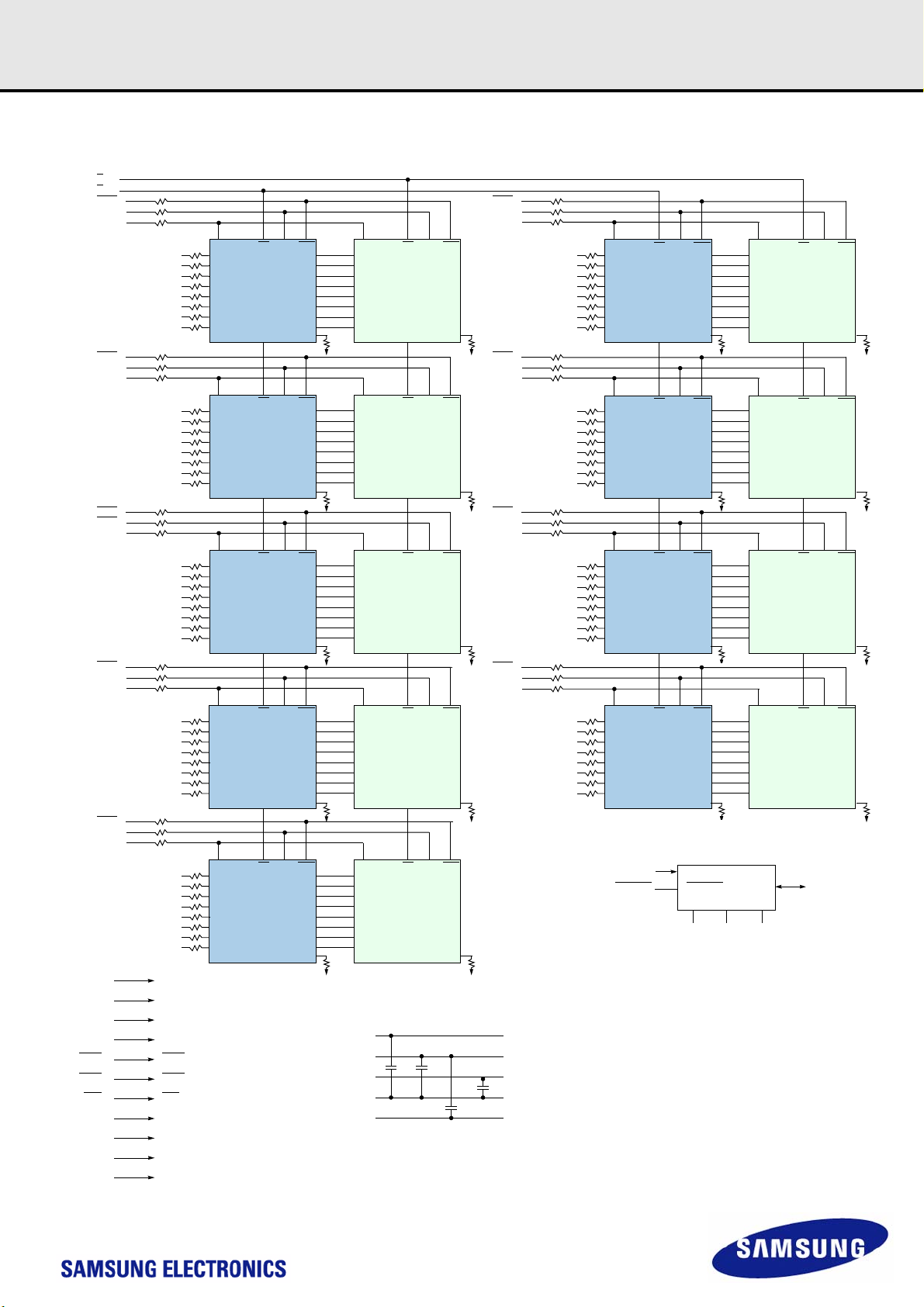
8. Function Block Diagram:
8.1 2GB, 256Mx72 ECC Module (Populated as 1 rank of x8 DDR3 SDRAMs)
S0
DQS0
DQS0
DM0
DM CS DQS DQS
DQS1
DQS1
DM1
DQS2
DQS2
DM2
DQS3
DQS3
DM3
DQS8
DQS8
DM8
DQ0
DQ1
DQ2
DQ3
DQ4
DQ5
DQ6
DQ7
DQ8
DQ9
DQ10
DQ11
DQ12
DQ13
DQ14
DQ15
DQ16
DQ17
DQ18
DQ19
DQ20
DQ21
DQ22
DQ23
DQ24
DQ25
DQ26
DQ27
DQ28
DQ29
DQ30
DQ31
CB0
CB1
CB2
CB3
CB4
CB5
CB6
CB7
I/O 0
I/O 1
D0
I/O 2
I/O 3
I/O 4
I/O 5
I/O 6
I/O 7
DM CS DQS DQS
I/O 0
I/O 1
D1
I/O 2
I/O 3
I/O 4
I/O 5
I/O 6
I/O 7
DM CS DQS DQS
I/O 0
I/O 1
D2
I/O 2
I/O 3
I/O 4
I/O 5
I/O 6
I/O 7
DM CS DQS DQS
I/O 0
I/O 1
D3
I/O 2
I/O 3
I/O 4
I/O 5
I/O 6
I/O 7
DM CS DQS DQS
I/O 0
I/O 1
D8
I/O 2
I/O 3
I/O 4
I/O 5
I/O 6
I/O 7
BA0 - BA2 BA0-BA2 : SDRAMs D0 - D8
A0 - A15 A0-A15 : SDRAMs D0 - D8
RAS
CAS
RAS : SDRAMs D0 - D8
CAS : SDRAMs D0 - D8
CKE0 CKE : SDRAMs D0 - D8
WE
WE : SDRAMs D0 - D8
ODT0 ODT : SDRAMs D0 - D8
CK0 CK : SDRAMs D0 - D8
ZQ
ZQ
ZQ
ZQ
ZQ
V
DDSPD SPD
VDD/V
DDQ
V
REFDQ
V
SS
V
REFCA
D0 - D8
D0 - D8
D0 - D8
D0 - D8
DQS4
DQS4
DM4
DQ32
DQ33
DQ34
DQ35
DQ36
DQ37
DQ38
DQ39
DQS5
DQS5
DM5
DQ40
DQ41
DQ42
DQ43
DQ44
DQ45
DQ46
DQ47
DQS6
DQS6
DM6
DQ48
DQ49
DQ50
DQ51
DQ52
DQ53
DQ54
DQ55
DQS7
DQS7
DM7
DQ56
DQ57
DQ58
DQ59
DQ60
DQ61
DQ62
DQ63
Serial PD
SCL
EVENTEVENT
A0
SA0 SA1
NOTE :
1. For each DRAM, a unique ZQ resistor is connected to
ground. The ZQ resistor is 240 Ohm +/- 1%
2. Refer to "SPD and Thermal sensor for ECC UDIMMs"
for SPD detail.
DM CS DQS DQS
I/O 0
I/O 1
D4
I/O 2
I/O 3
I/O 4
I/O 5
I/O 6
I/O 7
DM CS DQS DQS
I/O 0
I/O 1
D5
I/O 2
I/O 3
I/O 4
I/O 5
I/O 6
I/O 7
DM CS DQS DQS
I/O 0
I/O 1
D6
I/O 2
I/O 3
I/O 4
I/O 5
I/O 6
I/O 7
DM CS DQS DQS
I/O 0
I/O 1
D7
I/O 2
I/O 3
I/O 4
I/O 5
I/O 6
I/O 7
A1
A2
SA2
ZQ
ZQ
ZQ
ZQ
SDA
- 9 -
Rev. 1.0
Unbuffered DIMM
datasheet DDR3L SDRAM
8.2 4GB, 512Mx72 ECC Module (Populated as 2 ranks of x8 DDR3 SDRAMs)
S1
S0
DQS0
DQS0
DM0
DM CS DQS DQS
I/O 0
I/O 1
D0
I/O 2
I/O 3
I/O 4
I/O 5
I/O 6
I/O 7
DM CS DQS DQS
I/O 0
I/O 1
D1
I/O 2
I/O 3
I/O 4
I/O 5
I/O 6
I/O 7
DM CS DQS DQS
I/O 0
I/O 1
D2
I/O 2
I/O 3
I/O 4
I/O 5
I/O 6
I/O 7
DM CS DQS DQS
I/O 0
I/O 1
D3
I/O 2
I/O 3
I/O 4
I/O 5
I/O 6
I/O 7
DM CS DQS DQS
I/O 0
I/O 1
D8
I/O 2
I/O 3
I/O 4
I/O 5
I/O 6
I/O 7
DQS1
DQS1
DM1
DQS2
DQS2
DM2
DQS3
DQS3
DM3
DQS8
DQS8
DM8
DQ0
DQ1
DQ2
DQ3
DQ4
DQ5
DQ6
DQ7
DQ8
DQ9
DQ10
DQ11
DQ12
DQ13
DQ14
DQ15
DQ16
DQ17
DQ18
DQ19
DQ20
DQ21
DQ22
DQ23
DQ24
DQ25
DQ26
DQ27
DQ28
DQ29
DQ30
DQ31
CB0
CB1
CB2
CB3
CB4
CB5
CB6
CB7
BA0 - BA2 BA0-BA2 : SDRAMs D0 - D17
A0 - A15 A0-A15 : SDRAMs D0 - D17
CKE1 CKE : SDRAMs D9 - D17
CKE0 CKE : SDRAMs D0 - D8
RAS
CAS
WE
RAS : SDRAMs D0 - D17
CAS : SDRAMs D0 - D17
WE : SDRAMs D0 - D17
ODT0 ODT : SDRAMs D0 - D8
ODT1 ODT : SDRAMs D9 - D17
CK0 CK : SDRAMs D0 - D8
CK1 CK : SDRAMs D9 - D17
DM CS DQS DQS
I/O 0
I/O 1
D9
I/O 2
I/O 3
I/O 4
I/O 5
I/O 6
ZQ
ZQ
ZQ
ZQ
ZQ
I/O 7
DM CS DQS DQS
I/O 0
I/O 1
D10
I/O 2
I/O 3
I/O 4
I/O 5
I/O 6
I/O 7
DM CS DQS DQS
I/O 0
I/O 1
D11
I/O 2
I/O 3
I/O 4
I/O 5
I/O 6
I/O 7
DM CS DQS DQS
I/O 0
I/O 1
D12
I/O 2
I/O 3
I/O 4
I/O 5
I/O 6
I/O 7
DM CS DQS DQS
I/O 0
I/O 1
D17
I/O 2
I/O 3
I/O 4
I/O 5
I/O 6
I/O 7
V
DDSPD SPD
V
DD/VDDQ
V
REFDQ
V
SS
V
REFCA
ZQ
ZQ
ZQ
ZQ
ZQ
DQS4
DQS4
DM4
DQS5
DQS5
DM5
DQS6
DQS6
DM6
DQS7
DQS7
DM7
D0 - D17
D0 - D17
D0 - D17
D0 - D17
DQ32
DQ33
DQ34
DQ35
DQ36
DQ37
DQ38
DQ39
DQ40
DQ41
DQ42
DQ43
DQ44
DQ45
DQ46
DQ47
DQ48
DQ49
DQ50
DQ51
DQ52
DQ53
DQ54
DQ55
DQ56
DQ57
DQ58
DQ59
DQ60
DQ61
DQ62
DQ63
DM CS DQS DQS
I/O 0
I/O 1
I/O 2
I/O 3
I/O 4
I/O 5
I/O 6
I/O 7
DM CS DQS DQS
I/O 0
I/O 1
I/O 2
I/O 3
I/O 4
I/O 5
I/O 6
I/O 7
DM CS DQS DQS
I/O 0
I/O 1
I/O 2
I/O 3
I/O 4
I/O 5
I/O 6
I/O 7
DM CS DQS DQS
I/O 0
I/O 1
I/O 2
I/O 3
I/O 4
I/O 5
I/O 6
I/O 7
SCL
NOTE :
1. For each DRAM, a unique ZQ resistor is connected to
ground. The ZQ resistor is 240 Ohm +/- 1%
2. Refer to "SPD and Thermal sensor for ECC UDIMMs"
for SPD detail.
D4
D5
D6
D7
ZQ
ZQ
ZQ
ZQ
Serial PD
EVENTEVENT
A0
A1
SA0 SA1
DM CS DQS DQS
I/O 0
I/O 1
D13
I/O 2
I/O 3
I/O 4
I/O 5
I/O 6
I/O 7
DM CS DQS DQS
I/O 0
I/O 1
I/O 2
I/O 3
I/O 4
I/O 5
I/O 6
I/O 7
DM CS DQS DQS
I/O 0
I/O 1
I/O 2
I/O 3
I/O 4
I/O 5
I/O 6
I/O 7
DM CS DQS DQS
I/O 0
I/O 1
I/O 2
I/O 3
I/O 4
I/O 5
I/O 6
I/O 7
ZQ
D14
ZQ
D15
ZQ
D16
ZQ
SDA
A2
SA2
- 10 -
Rev. 1.0
Unbuffered DIMM
datasheet DDR3L SDRAM
9. Absolute Maximum Ratings
9.1 Absolute Maximum DC Ratings
Symbol Parameter Rating Units NOTE
V
DD
V
Voltage on V
DDQ
V
NOTE :
1. Stresses greater than those listed under “Absolute Maximum Ratings” may cause permanent damage to the device. This is a stress rating only and functional operation of the
device at these or any other conditions above those indicated in the operational sections of this specification is not implied. Exposure to absolute maximum rating conditions
for extended periods may affect reliability.
2. Storage Temperature is the case surface temperature on the center/top side of the DRAM. For the measurement conditions, please refer to JESD51-2 standard.
3. VDD and V
equal to or less than 300mV.
Voltage on any pin relative to V
IN, VOUT
T
Storage Temperature -55 to +100 °C 1, 2
STG
DDQ
Voltage on VDD pin relative to V
pin relative to V
DDQ
must be within 300mV of each other at all times;and V
SS
SS
SS
must be not greater than 0.6 x V
REF
9.2 DRAM Component Operating Temperature Range
Symbol Parameter rating Unit NOTE
T
OPER
NOTE :
1. Operating Temperature T
JESD51-2.
2. The Normal Temperature Range specifies the temperatures where all DRAM specifications will be supported. During operation, the DRAM case temperature must be maintained between 0-85°C under all operating conditions
3. Some applications require operation of the Extended Temperature Range between 85°C and 95°C case temperature. Full specifications are guaranteed in this range, but the
following additional conditions apply:
a) Refresh commands must be doubled in frequency, therefore reducing the refresh interval tREFI to 3.9us. It is also possible to specify a component with 1X refresh (tREFI
to 7.8us) in the Extended Temperature Range.
b) If Self-Refresh operation is required in the Extended Temperature Range, then it is mandatory to either use the Manual Self-Refresh mode with Extended Temperature
Range capability (MR2 A6 = 0b and MR2 A7 = 1b), in this case IDD6 current can be increased around 10~20% than normal Temperature range.
is the case surface temperature on the center/top side of the DRAM. For measurement conditions, please refer to the JEDEC document
OPER
Operating Temperature Range 0 to 95 °C 1, 2, 3
-0.4 V ~ 1.975 V V 1,3
-0.4 V ~ 1.975 V V 1,3
-0.4 V ~ 1.975 V V 1
, When VDD and V
DDQ
are less than 500mV; V
DDQ
REF
may be
10. AC & DC Operating Conditions
10.1 Recommended DC Operating Conditions (SSTL-15)
Symbol Parameter Operation Voltage
V
DD
V
DDQ
NOTE:
1. Under all conditions V
2. V
tracks with VDD. AC parameters are measured with VDD and V
DDQ
3. V
& V
DD
DDQ
Supply Voltage
Supply Voltage for Output
must be less than or equal to VDD.
DDQ
rating are determinied by operation voltage.
1.35V 1.283 1.35 1.45 V 1, 2, 3
1.5V 1.425 1.5 1.575 V 1, 2, 3
1.35V 1.283 1.35 1.45 V 1, 2, 3
1.5V 1.425 1.5 1.575 V 1, 2, 3
tied together.
DDQ
Min. Typ . Max.
Rating
Units NOTE
- 11 -
 Loading...