

SERIAL PRESENCE DETECT
M378A4G43MB1-CTD
Organization : 1G x 64
Composition : 1Gb x8 *16ea
Used component part # : K4A8G085WD-BCTDM00
# of rows in module : 2Rows
# of banks in component : 4Banks 4BG
Feature : 31.25mm height & Double sided component
Refresh : 8K/64ms
Bin Sort : TD(DDR4 2666@CL=19)
RCD Vendor and Revision : N/A
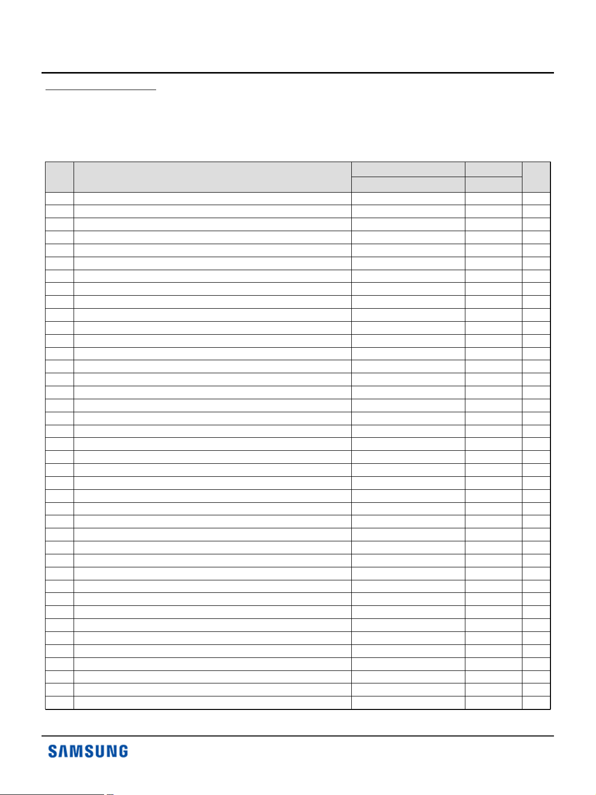
Byte
#
0 Number of Bytes Used / Number of Bytes in SPD Device / CRC Coverage 512B Total, 384B Used 23h
1 SPD Revision Ver 1.1 11h
2 Key Byte / DRAM Device Type DDR4 SDRAM 0Ch
3 Key Byte / Module Type UDIMM 02h
4 SDRAM Density and Banks 16Gb,4BG&4Banks 86h
5 SDRAM Addressing Row bits 17,Column bits 10 29h
6 SDRAM Device Type Monolithinc Device 00h
7 SDRAM Optional Features Unlimited MAC 08h
8 SDRAM Thermal and Refresh Option Reserved 00h
9 Other SDRAM Optional Features sPPR supported 60h
10 Reserved Reserved 00h
11 Module Nominal Voltage, VDD 1.2V 03h
12 Module Organization 2Rx8 09h
13 Module Memory Bus Width 64bit, Non-ECC 03h
14 Module Thermal Sensor without TS 00h
15~16 Reserved Reserved 00h
17 Timebases MTB 125ps, FTB 1ps 00h
18 SDRAM Minimum Cycle Time(tckavg min) 0.750ns 06h
19 SDRAM Minimum Cycle Time(tckavg max) 1.6ns 0Dh
20 Cas Latency Supported, First Byte 10,11,12,13,14,15,16,17,18, 19,20 F8h
21 Cas Latency Supported, Second Byte 10,11,12,13,14,15,16,17,18, 19,20 3Fh
22 Cas Latency Supported, Third Byte 10,11,12,13,14,15,16,17,18, 19,20 00h
23 Cas Latency Supported, Fourth Byte 10,11,12,13,14,15,16,17,18, 19,20 00h
24 Minimum Cas Latency Time (tAAmin) 13.75ns 6Eh
25 Minimum RAS to CAS Delay Time(tRCD min) 13.75ns 6Eh
26 Minimum Raw Precharge Delay Time(tRP min) 13.75ns 6Eh
27 Upper Nibbles for tRASmin and tRCmin tRAS=32ns,tRC=45.75ns 11h
28 Minimum Active to Precharge Delay Time (tRASmin), Least Significant Byte tRAS=32ns 00h
29 Minimum Active to Active/Refresh Delay Time (tRCmin), Least Significant Byte tRC=45.75ns 6Eh
30 Minimum Refresh Recovery Delay Time (tRFC1min), LSB 550ns 30h
31 Minimum Refresh Recovery Delay Time (tRFC1min), MSB 550ns 11h
32 Minimum Refresh Recovery Delay Time (tRFC2min), LSB 350ns F0h
33 Minimum Refresh Recovery Delay Time (tRFC2min), MSB 350ns 0Ah
34 Minimum Refresh Recovery Delay Time (tRFC4min), LSB 260ns 20h
35 Minimum Refresh Recovery Delay Time (tRFC4min), MSB 260ns 08h
36 Minimum Four Active Window Time (tFAWmin), Most Significant Nibble 21ns 00h
37 Minimum Four Activate Window Time (tFAWmin), Least Significant Byte 21ns A8h
38 Minimum Active to Active Delay Time (tRRD_smin), different Bank Group 3.0ns 18h
39 Minimum Active to Active Delay Time (tRRD_Lmin), Same Bank Group 4.9ns 28h
40 Minimum CAS to CAS Delay Time(tCCD_Lmin), same bank group 5ns 28h
Function Described
Function Supported Hex Value
CTD CTD
Note
JUL. 2018
SERIAL PRESENCE DETECT
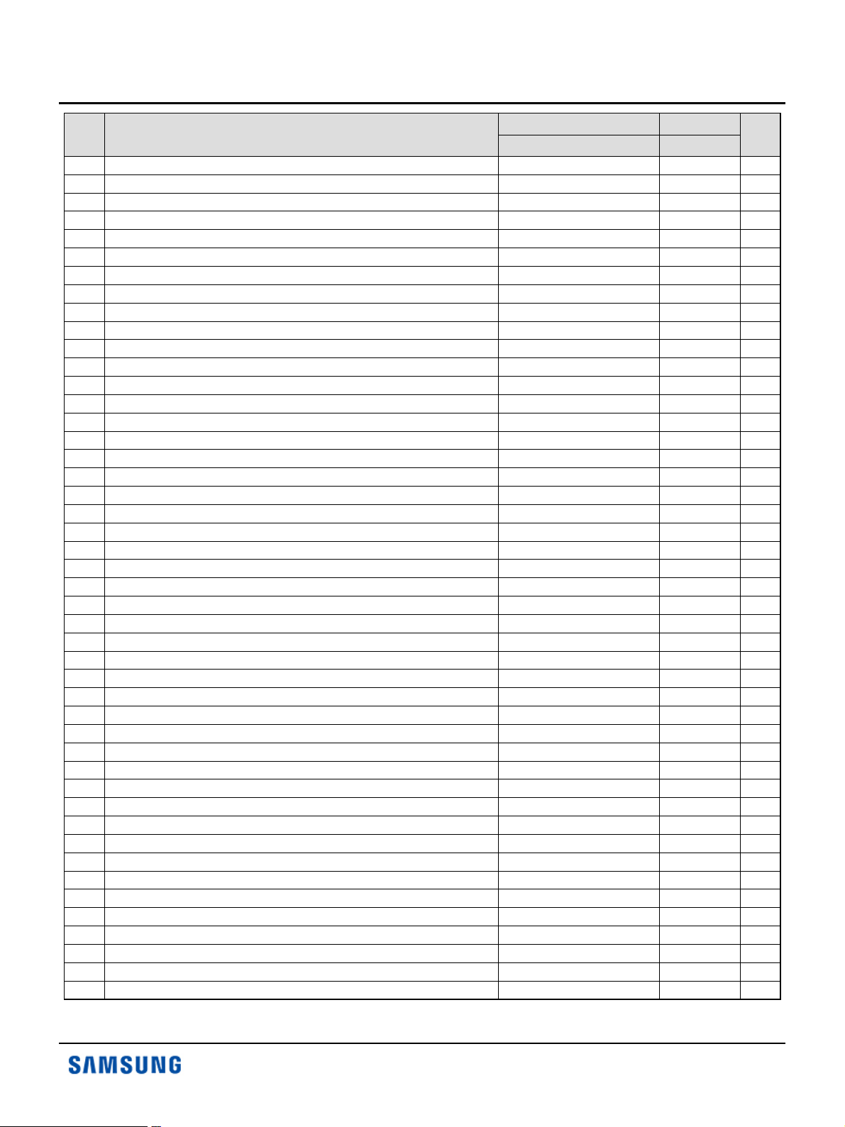
Byte
#
41 Upper Nibble for tWRmin 15ns 00h
42 Minimum Write Recovery Time(tWRmin) 15ns 78h
43 Upper Nibbles for tWTRmin 2.5ns 00h
44 Minimum Write to Read Time(tWTR_smin), different bank group 2.5ns 14h
45 Minimum Write to Read Time(tWTR_Lmin), same bank group 7.5ns 3Ch
46~59 Reserved Reserved 00h
60 Connector to SDRAM Bit Mapping DQ0-3 (NECC UDIMM R/C B1) 15h
61 Connector to SDRAM Bit Mapping DQ4-7(NECC UDIMM R/C B1) 2Bh
62 Connector to SDRAM Bit Mapping DQ8-11(NECC UDIMM R/C B1) 16h
63 Connector to SDRAM Bit Mapping DQ 12-15(NECC UDIMM R/C B1) 36h
64 Connector to SDRAM Bit Mapping DQ 16-19(NECC UDIMM R/C B1) 0Bh
65 Connector to SDRAM Bit Mapping DQ20-23(NECCUDIMMR/CB1) 2Bh
66 Connector to SDRAM Bit Mapping DQ 24-27(NECC UDIMM R/C B1) 0Ch
67 Connector to SDRAM Bit Mapping DQ 28-31(NECC UDIMM R/C B1) 36h
68 Connector to SDRAM Bit Mapping CB0-3(NECC) 00h
69 Connector to SDRAM Bit Mapping CB4-7(NECC) 00h
70 Connector to SDRAM Bit Mapping DQ 32-35(NECC UDIMM R/C B1) 36h
71 Connector to SDRAM Bit Mapping DQ 36-39(NECC UDIMM R/C B1) 15h
72 Connector to SDRAM Bit Mapping DQ 40-43(NECC UDIMM R/C B1) 2Bh
73 Connector to SDRAM Bit Mapping DQ44-47(NECCUDIMMR/CB1) 0Ch
74 Connector to SDRAM Bit Mapping DQ 48-51(NECC UDIMM R/C B1) 2Ch
75 Connector to SDRAM Bit Mapping DQ 52-55(NECC UDIMM R/C B1) 16h
76 Connector to SDRAM Bit Mapping DQ 56-59(NECC UDIMM R/C B1) 2Bh
77 Connector to SDRAM Bit Mapping DQ60-63 (NECC UDIMM R/C B1) 0Ch
78~116 Reserved reserved 00h
117 Fine Offset for Minimum CAS to CAS Delay Time(tCCD_Lmin), same bank group 5ns 00h
118 Fine Offset for Minimum Activate to Acticate Delay Time(tRRD_L_min), Same Bank Group 4.9ns 9Ch
119 Fine Offset for Minimum Activate to Acticate Delay Time(tRRD_Smin), Different Bank Group 3.0ns 00h
120 Fine Offset for Minimum Activate to Acticate/Refresh Delay Time(tRCmin) 45.75ns 00h
121 Fine Offset for Minimum Row Precharge Delay Time(tRPmin) 13.75ns 00h
122 Fine Offset for Minimum RAS to CAS Delay Time(tRCD_min) 13.75ns 00h
123 Fine Offset for Minimum CAS Latency Delay Time(tAA_min) 13.75ns 00h
124 Fine Offset for DRAM Maximum Cycle Time(tCKAVG_max) 1.6ns E7h
125 Fine Offset for DRAM Minimum Cycle Time(tCKAVG_min) 0.750ns 00h
126 Cyclical Redundancy Code - 48h
127 Cyclical Redundancy Code - 03h
128 Raw Card Extension, Module Nominal Height R/C B 1.0, 31.25mm 11h
129 Module Maximum Thickness (Eachside)1<thickness<2mm 11h
130 Reference Raw Card Used R/C B 1.0 21h
131 Address Mapping from Edge Connector to DRAM Mirrored 01h
132~253 Reserved Reserved 00h
254 Cyclical Redundancy Code - 74h
255 Cyclical Redundancy Code - DFh
256~319 Reserved Reserved 00h
320 Module Manufacturer's ID Code, Least Significant Byte Samsung 80h
321 Module Manufacturer's ID Code, Most Significant Byte Samsung CEh
Function Described
Function Supported Hex Value
CTD CTD
Note
JUL. 2018
 Loading...