

Page 1

User Manual
FLEX I/O PROFIBUS Adapter Module
Catalog Number
1794-APBDPV1
Page 2
Important User Information
IMPORTANT
Solid-state equipment has operational characteristics differing from those of electromechanical equipment. Safety
Guidelines for the Application, Installation and Maintenance of Solid State Controls (publication SGI-1.1
your local Rockwell Automation sales office or online at http://www.rockwellautomation.com/literature/
important differences between solid-state equipment and hard-wired electromechanical devices. Because of this difference,
and also because of the wide variety of uses for solid-state equipment, all persons responsible for applying this equipment
must satisfy themselves that each intended application of this equipment is acceptable.
In no event will Rockwell Automation, Inc. be responsible or liable for indirect or consequential damages resulting from
the use or application of this equipment.
The examples and diagrams in this manual are included solely for illustrative purposes. Because of the many variables and
requirements associated with any particular installation, Rockwell Automation, Inc. cannot assume responsibility or
liability for actual use based on the examples and diagrams.
No patent liability is assumed by Rockwell Automation, Inc. with respect to use of information, circuits, equipment, or
software described in this manual.
Reproduction of the contents of this manual, in whole or in part, without written permission of Rockwell Automation,
Inc., is prohibited.
Throughout this manual, when necessary, we use notes to make you aware of safety considerations.
WARNING: Identifies information about practices or circumstances that can cause an explosion in a hazardous
environment, which may lead to personal injury or death, property damage, or economic loss.
available from
) describes some
ATTENTION: Identifies information about practices or circumstances that can lead to personal injury or death,
property damage, or economic loss. Attentions help you identify a hazard, avoid a hazard, and recognize the
consequence
SHOCK HAZARD: Labels may be on or inside the equipment, for example, a drive or motor, to alert people that
dangerous voltage may be present.
BURN HAZARD: Labels may be on or inside the equipment, for example, a drive or motor, to alert people that
surfaces may reach dangerous temperatures.
Identifies information that is critical for successful application and understanding of the product.
Allen-Bradley, Rockwell Automation, FLEX I/O, RSLogix, R SLinx, and TechConnect are trademarks of Rockwell Automation, Inc.
Trademarks not belonging to Rockwell Automation are property of their respective companies.
Page 3

Summary of Changes
The information below summarizes the changes to this manual since the last
printing.
To help you find new and updated information in this release of the manual, we
have included change bars as shown next to this paragraph.
The table below lists the sections that document new features and additional or
updated information about existing features.
Top ic
Added detailed procedure for using the teaching feature and the different
parameters for creating a teaching entry
Page
105
Rockwell Automation Publication 1763-UM002D-EN-P - May 2014 iii
Page 4

Chapter 1
Notes:
iv Rockwell Automation Publication 1763-UM002D-EN-P - May 2014
Page 5

Overview of the FLEX I/O
PROFIBUS APBDPV1 Module
Table of Contents
Preface
Who Should Use this Manual . . . . . . . . . . . . . . . . . . . . . . . . . . . . . . . . . . . . . . . v
Purpose of this Manual . . . . . . . . . . . . . . . . . . . . . . . . . . . . . . . . . . . . . . . . . . . . . v
Related Documentation. . . . . . . . . . . . . . . . . . . . . . . . . . . . . . . . . . . . . . . . vi
Common Techniques Used in this Manual . . . . . . . . . . . . . . . . . . . . . . . . . vii
Chapter 1
Overview . . . . . . . . . . . . . . . . . . . . . . . . . . . . . . . . . . . . . . . . . . . . . . . . . . . . . . . . . 1
The FLEX I/O System. . . . . . . . . . . . . . . . . . . . . . . . . . . . . . . . . . . . . . . . . . . . . 1
Purpose of the FLEX I/O PROFIBUS APBDPV1 Adapter. . . . . . . . . . . 2
Differences Between APB and APBDPV1 Adapters . . . . . . . . . . . . . . . . . . 2
DP-V1 Protocol . . . . . . . . . . . . . . . . . . . . . . . . . . . . . . . . . . . . . . . . . . . . . . . 2
Functionality. . . . . . . . . . . . . . . . . . . . . . . . . . . . . . . . . . . . . . . . . . . . . . . . . . 2
Bandwidth and Range. . . . . . . . . . . . . . . . . . . . . . . . . . . . . . . . . . . . . . . . . . 3
PROFIBUS APBDPV1 Adapter Components. . . . . . . . . . . . . . . . . . . . . . . 3
Diagnostic Indicators . . . . . . . . . . . . . . . . . . . . . . . . . . . . . . . . . . . . . . . . . . 3
Network Connector . . . . . . . . . . . . . . . . . . . . . . . . . . . . . . . . . . . . . . . . . . . 3
Set the Node Address Switches . . . . . . . . . . . . . . . . . . . . . . . . . . . . . . . . . 4
Power Wiring . . . . . . . . . . . . . . . . . . . . . . . . . . . . . . . . . . . . . . . . . . . . . . . . . 4
Mount and Remove Your System . . . . . . . . . . . . . . . . . . . . . . . . . . . . . . . . . . . 4
Optional Accessories . . . . . . . . . . . . . . . . . . . . . . . . . . . . . . . . . . . . . . . . . . . . . . 5
Extender Cables (1794-CE1 or -CE3) . . . . . . . . . . . . . . . . . . . . . . . . . . . 5
Mounting Kit (1794-NM1) . . . . . . . . . . . . . . . . . . . . . . . . . . . . . . . . . . . . 6
Mounting Dimensions and Spacing Requirements . . . . . . . . . . . . . . . . . . . 7
Chapter Summary. . . . . . . . . . . . . . . . . . . . . . . . . . . . . . . . . . . . . . . . . . . . . . . . . 7
Chapter 2
Communicate With Your
Module
Overview . . . . . . . . . . . . . . . . . . . . . . . . . . . . . . . . . . . . . . . . . . . . . . . . . . . . . . . . . 9
Communication Over the I/O Backplane . . . . . . . . . . . . . . . . . . . . . . . . . . . 9
Polled I/O Structure. . . . . . . . . . . . . . . . . . . . . . . . . . . . . . . . . . . . . . . . . . . . . . 10
Adapter Input Status Word . . . . . . . . . . . . . . . . . . . . . . . . . . . . . . . . . . . 10
Map Data into the Image Table. . . . . . . . . . . . . . . . . . . . . . . . . . . . . . . . . . . . 12
Logic Status/Analog Feedback Definition . . . . . . . . . . . . . . . . . . . . . . 67
Logic Command/Analog Reference Definition . . . . . . . . . . . . . . . . . 68
Defaults . . . . . . . . . . . . . . . . . . . . . . . . . . . . . . . . . . . . . . . . . . . . . . . . . . . . . . . . . 68
Chapter Summary. . . . . . . . . . . . . . . . . . . . . . . . . . . . . . . . . . . . . . . . . . . . . . . . 69
Chapter 3
Connect Your Adapter to the
PROFIBUS DP Network
v Publication 1794-UM064B-EN-P - May 2014
Overview . . . . . . . . . . . . . . . . . . . . . . . . . . . . . . . . . . . . . . . . . . . . . . . . . . . . . . . . 71
The DP Physical Layer. . . . . . . . . . . . . . . . . . . . . . . . . . . . . . . . . . . . . . . . . . . . 71
Cabling and Equipment Required for Line A Type. . . . . . . . . . . . . . . . . . 72
Cables . . . . . . . . . . . . . . . . . . . . . . . . . . . . . . . . . . . . . . . . . . . . . . . . . . . . . . . 72
T-junction Connectors . . . . . . . . . . . . . . . . . . . . . . . . . . . . . . . . . . . . . . . 72
Termination Blocks. . . . . . . . . . . . . . . . . . . . . . . . . . . . . . . . . . . . . . . . . . . 72
Page 6

vi Table of Contents
Bus Connector . . . . . . . . . . . . . . . . . . . . . . . . . . . . . . . . . . . . . . . . . . . . . . . 73
Cabling and Equipment Required for Line B Type . . . . . . . . . . . . . . . . . . 73
Cables . . . . . . . . . . . . . . . . . . . . . . . . . . . . . . . . . . . . . . . . . . . . . . . . . . . . . . . 73
T-junction Connectors . . . . . . . . . . . . . . . . . . . . . . . . . . . . . . . . . . . . . . . 73
Termination Blocks. . . . . . . . . . . . . . . . . . . . . . . . . . . . . . . . . . . . . . . . . . . 73
Bus Connector . . . . . . . . . . . . . . . . . . . . . . . . . . . . . . . . . . . . . . . . . . . . . . . 73
Connect the Adapter to the Network . . . . . . . . . . . . . . . . . . . . . . . . . . . . . . 74
Connect Wiring to the Adapter. . . . . . . . . . . . . . . . . . . . . . . . . . . . . . . . 74
Terminate the Network. . . . . . . . . . . . . . . . . . . . . . . . . . . . . . . . . . . . . . . . . . . 76
Terminate at the Adapter Using Line A . . . . . . . . . . . . . . . . . . . . . . . . 76
Terminate at the Adapter Using Line B. . . . . . . . . . . . . . . . . . . . . . . . . 77
Chapter Summary. . . . . . . . . . . . . . . . . . . . . . . . . . . . . . . . . . . . . . . . . . . . . . . . 77
Chapter 4
Configure the Adapter for
Master/Slave Communication
Interpret Status Indicators for
the FLEX I/O PROFIBUS Module
Apply FLEX I/O Modules
Overview . . . . . . . . . . . . . . . . . . . . . . . . . . . . . . . . . . . . . . . . . . . . . . . . . . . . . . . . 79
How Master/Slave Communication Takes Place . . . . . . . . . . . . . . . . . . . . 79
Enter User Parameter Data. . . . . . . . . . . . . . . . . . . . . . . . . . . . . . . . . . . . . . . . 80
User Parameter Data. . . . . . . . . . . . . . . . . . . . . . . . . . . . . . . . . . . . . . . . . . 80
Auto Configure Format . . . . . . . . . . . . . . . . . . . . . . . . . . . . . . . . . . . . . . . 81
Condensed Format . . . . . . . . . . . . . . . . . . . . . . . . . . . . . . . . . . . . . . . . . . . 81
Full Format . . . . . . . . . . . . . . . . . . . . . . . . . . . . . . . . . . . . . . . . . . . . . . . . . . 84
Enter Check Configuration Data . . . . . . . . . . . . . . . . . . . . . . . . . . . . . . . . . . 86
Chapter Summary. . . . . . . . . . . . . . . . . . . . . . . . . . . . . . . . . . . . . . . . . . . . . . . . 89
Chapter 5
Overview . . . . . . . . . . . . . . . . . . . . . . . . . . . . . . . . . . . . . . . . . . . . . . . . . . . . . . . . 91
Status Indicators . . . . . . . . . . . . . . . . . . . . . . . . . . . . . . . . . . . . . . . . . . . . . . . . . 91
1794-APBDPV1 Module . . . . . . . . . . . . . . . . . . . . . . . . . . . . . . . . . . . . . 91
View status from the Master’s Configuration Software . . . . . . . . . . . . . . 92
Chapter Summary. . . . . . . . . . . . . . . . . . . . . . . . . . . . . . . . . . . . . . . . . . . . . . . . 93
Chapter 6
Overview . . . . . . . . . . . . . . . . . . . . . . . . . . . . . . . . . . . . . . . . . . . . . . . . . . . . . . . . 95
Evaluate the Application . . . . . . . . . . . . . . . . . . . . . . . . . . . . . . . . . . . . . . . . . . 95
Define the Area Classification . . . . . . . . . . . . . . . . . . . . . . . . . . . . . . . . . . . . . 96
Decide Classification Method . . . . . . . . . . . . . . . . . . . . . . . . . . . . . . . . . 96
Determine Hazard. . . . . . . . . . . . . . . . . . . . . . . . . . . . . . . . . . . . . . . . . . . . 96
Determine Temperature Rating. . . . . . . . . . . . . . . . . . . . . . . . . . . . . . . . 96
Select Protection Method(s). . . . . . . . . . . . . . . . . . . . . . . . . . . . . . . . . . . . . . . 97
Match Field Devices
and I/O Modules. . . . . . . . . . . . . . . . . . . . . . . . . . . . . . . . . . . . . . . . . . . . . . . . . 97
P/I Analog Transmitter Functional and IS Parameters . . . . . . . . . . . 98
Loop Functionality Verification . . . . . . . . . . . . . . . . . . . . . . . . . . . . . . . 98
Chapter Summary. . . . . . . . . . . . . . . . . . . . . . . . . . . . . . . . . . . . . . . . . . . . . . . . 99
Publication 1794-UM064B-EN-P - May 2014
Page 7

Specifications
Table of Contents vii
Appendix A
Overview . . . . . . . . . . . . . . . . . . . . . . . . . . . . . . . . . . . . . . . . . . . . . . . . . . . . . . . 101
Appendix B
Device Data Base (GSD) File
Additional HART Protocol
Information
Overview . . . . . . . . . . . . . . . . . . . . . . . . . . . . . . . . . . . . . . . . . . . . . . . . . . . . . . . 105
Use the Teaching GSD Feature. . . . . . . . . . . . . . . . . . . . . . . . . . . . . . . . . . . 105
Create Standard and Teaching GSD Files. . . . . . . . . . . . . . . . . . . . . . 106
Teaching GSD Entry. . . . . . . . . . . . . . . . . . . . . . . . . . . . . . . . . . . . . . . . . 107
Teach an I/O Module to Work with 1794-APBDPV1 Adapter . . . . . 115
Appendix C
Overview . . . . . . . . . . . . . . . . . . . . . . . . . . . . . . . . . . . . . . . . . . . . . . . . . . . . . . . 121
Message Structure . . . . . . . . . . . . . . . . . . . . . . . . . . . . . . . . . . . . . . . . . . . . . . . 121
Master-slave Operation . . . . . . . . . . . . . . . . . . . . . . . . . . . . . . . . . . . . . . 121
Multiple Master Operation. . . . . . . . . . . . . . . . . . . . . . . . . . . . . . . . . . . 121
Transaction Procedure . . . . . . . . . . . . . . . . . . . . . . . . . . . . . . . . . . . . . . . 121
Burst Mode (not supported). . . . . . . . . . . . . . . . . . . . . . . . . . . . . . . . . . 122
Universal Commands. . . . . . . . . . . . . . . . . . . . . . . . . . . . . . . . . . . . . . . . . . . . 126
Index
Publication 1794-UM064B-EN-P - May 2014
Page 8

viii Table of Contents
Notes:
Publication 1794-UM064B-EN-P - May 2014
Page 9

Preface
Read this preface to familiarize yourself with the rest of the manual. It provides
information concerning:
• who should use this manual
• the purpose of this manual
• related documentation
• conventions used in this manual
Who Should Use this Manual
Purpose of this Manual
You must be able to program and operate a PROFIBUS product and PROFIBUS
network to make efficient use of the FLEX I/O PROFIBUS APBDPV1 adapter
module.
We assume you know how to do this in this manual. If you do not, refer to your
software user manuals or online help before attempting to use these modules.
This manual describes how you can use your FLEX I/O PROFIBUS APBDPV1
adapter with your controller. The manual helps you install, program, and
troubleshoot your module.
For Information About See
Overview of the FLEX I/O PROFIBUS APBDPV1 Module Chapter 1
Communicate With Your Module Chapter 2
Connect Your Adapter to the PROFIBUS DP Network Chapter 3
Configure the Adapter for Master/Slave Communication Chapter 4
Interpret Status Indicators for the FLEX I/O PROFIBUS Module Chapter 5
Apply FLEX I/O Modules Chapter 6
Specifications Appendix A
Device Data Base (GSD) File Appendix B
Additional HART Protocol Information Appendix C
ix Publication 1794-UM064B-EN-P - May 2014
Page 10

x
Related Documentation
The following documents contain additional information concerning Rockwell
Automation products.
Resource Description
FLEX I/O Selection Guide, publication 1794-SG002
Remote I/O Adapter Module User Manual, publication
1794–UM009
Remote I/O Adapter Modules Installation Instructions,
publication 1794-IN098
FLEX I/O PROFIBUS Adapter Module Installation
Instructions, publication 1794-IN087
FLEX I/O PROFIBUS Adapter Module User Manual,
publication 1794-UM057
FLEX I/O Terminal Base Units Installation Instructions,
publication 1794-IN092
FLEX I/O Digital Input Modules Installation Instructions,
publication 1794-IN093
FLEX I/O Digital DC Sourcing Input and Sinking Output
Modules Installation Instructions, publication
1794-IN095
FLEX I/O Digital DC Sourcing Output Modules
Installation Instructions, publication 1794-IN094
.
.
.
.
.
.
.
. A description and overview of the 1794 series FLEX I/O, FLEX I/O XT and
.
FLEX Ex modules and compatible control platforms.
Information on how to use the Remote I/O Adapter Module
Catalog No. 1794-ASB.
Information on how to install the Remote I/O Adapter Module
Catalog No. 1794-ASB, 1794-ASB2, 1794-ASBK, 1794-ASB2K
Information on how to install the FLEX I/O PROFIBUS Adapter
Catalog No. 1794-APB.
Information on how to use the FLEX I/O PROFIBUS Adapter Module
Catalog No. 1794-APB.
Information on how to install the FLEX I/O Terminal Base Units
Catalog No. 1794-TB2, 1794-TB3, 1794-TB3K, 1794-TB3S, 1794-TB32,
1794-TB3G, 1794-TB3GK, 1794-TB3GS, 1794-TB3T, 1794-TB3TS, 1794-TBN,
1794-TBNK, 1794-TBNF.
Information on how to install the FLEX I/O Digital Input Modules
Catalog No. 1794-IB8, 1794-IB16, 1794-IB16K, 1794-IB32
Information on how to install the FLEX I/O Digital Input and Output Modules
Catalog No. 1794-IV16, 1794-OV16, 1794-OV16P
Information on how to install the FLEX I/O Digital DC Sourcing Output Modules
Catalog No.1794-OB8, 1794-OB8EP, 1794-OB16, 1794-OB16P, 1794-OB32P
FLEX I/O Input/ Output Module Installation Instructions,
publication 1794-IN083
FLEX I/O 8 Output Relay Module Installation Instructions,
publication 1794-IN019
FLEX I/O Analog Input and Output Module Installation
Instructions, publication 1794-IN100
FLEX I/O Isolated Analog Output Module Installation
Instructions, publication 1794-IN037
FLEX XT I/O Isolated Input Analog Module Installation
Instructions, publication 1794-IN129
FLEX I/O Isolated Analog Modules User Manual,
publication 1794-6.5.8
FLEX I/O 8 Thermocouple Input Module Installation
Instructions, publication 1794-IN021
FLEX I/O Thermocouple/Millivolt Input Module
Installation Instructions, publication 1794-IN050
FLEX I/O Thermocouple/Millivolt Input Module User
Manual, publication 1794-6.5.7
Publication 1794-UM064B-EN-P - May 2014
.
.
.
.
.
.
.
.
.
Information on how to install the FLEX I/O Input and Output Modules
Catalog No.1794-IB16XOB16P, 1794-IB10XOB6
Information on how to install the FLEX I/O 8 Output Relay Modules
Catalog No.1794-OW8, 1794-OW8K, 1794-OW8XT
Information on how to install the FLEX I/O Analog Input and Output Modules
Catalog No.1794-IE8, 1794-IE4XOE2, 1794-OE4, 1794-IE8K, 1794-OE4K
Information on how to install the FLEX I/O Isolated Analog 4 Input Module
Catalog No.1794-OF4I
Information on how to install the FLEX I/O Isolated Analog Modules
Catalog No.1794-IF4IXT, 1794-OF4IXT, 1794-IF2XOF2IXT
Information on how to use the FLEX I/O Isolated Analog Modules
Catalog No.1794-IF4I, -OF4I, IF2XOF2I, -IF4IXT, -IF4ICFXT, -OF4IXT, IF2XOF2IXT
Information on how to install the FLEX I/O Isolated Analog Modules
Catalog No. 1794-IT8,1794-IR8
Information on how to install the Thermocouple/Millivolt Input Modules
Catalog No. 1794-IRT8, 1794-IRT8K, 1794-IRT8XT
Information on how to use the Thermocouple and Millivolt Input Module
Catalog No. 1794-IT8.
Page 11

Resource Description
xi
FLEX I/O AC Input Modules Installation Instructions,
publication 1794-IN102
FLEX I/O Digital AC Output Modules Installation
Instructions, publication 1794-IN103
FLEX I/O DC Power Supply Installation Instructions,
publication 1794-IN069
Interconnect Cable Installation Instructions, publication
1794-5.12
Industrial Automation Wiring and Grounding Guidelines,
publication 1770-4.1
Allen-Bradley Industrial Automation Glossary,
publication AG-7.1
.
Common Techniques Used in this Manual
.
.
.
.
.
The following conventions are used throughout this manual:
• Bulleted lists such as this one provide information, not procedural steps.
• Numbered lists provide sequential steps or hierarchical information.
• Italic type is used for emphasis.
Information on how to install the FLEX I/O AC Input Modules
Catalog No. 1794-IA8, 1794-IA8I, 1794-IA16.
Information on how to install the FLEX I/O Digital AC Output Modules
Catalog No. 1794-OA8, 1794-OA8K, 1794-OA8I, 1794-OA16.
Information on how to install the FLEX I/O DC Power Supply
Catalog No. 1794-PS13, 1794-PS3
Information on how to install the extension cables.
Catalog No. 1794--CE1, 1794-CE3
In-depth information on grounding and wiring Allen-Bradley programmable
controllers.
A glossary of industrial automation terms and abbreviations.
Publication 1794-UM064B-EN-P - May 2014
Page 12

xii
Notes:
Publication 1794-UM064B-EN-P - May 2014
Page 13
Chapter
Adapter I/O moduleTerminal base
1113
1112
1111
Overview of the FLEX I/O PROFIBUS APBDPV1 Module
1
Overview
The FLEX I/O System
Read this chapter to familiarize yourself with the adapter module.
For Information About See Page
The FLEX I/O System 1
Purpose of the FLEX I/O PROFIBUS APBDPV1 Adapter 2
Differences Between APB and APBDPV1 Adapters 2
PROFIBUS APBDPV1 Adapter Components 3
Mount and Remove Your System 4
Optional Accessories 5
Mounting Dimensions and Spacing Requirements 7
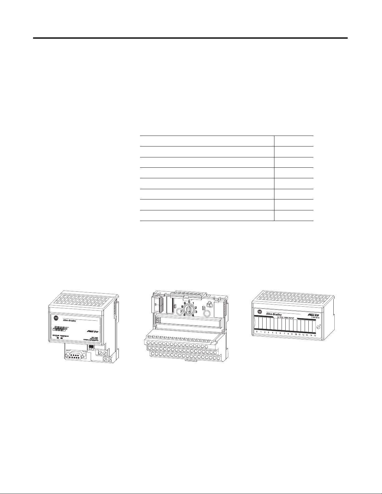
The FLEX I/O system is a small, modular I/O system for distributed
applications that performs all of the functions of rack-based I/O. The FLEX I/O
system contains the following components:
• PROFIBUS adapter/power supply – powers the internal logic for as many
as eight I/O modules
1 Publication 1794-UM064B-EN-P - May 2014
• terminal base – contains a terminal strip to terminate wiring for two- or
three-wire devices
• I/O module – contains the bus interface and circuitry needed to perform
specific functions related to your application
Page 14
2 Overview of the FLEX I/O PROFIBUS APBDPV1 Module
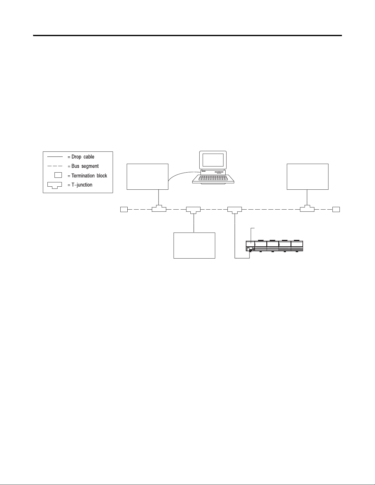
RS-485
PROFIBUS DP
master/scanner
controller
Other DP
adapter/slave
DP
1794-APBDPV1 adapter/slave
FLEX I/O system
Other DP
adapter/slave
Personal computer
with configuration
software
1118
Purpose of the FLEX I/O PROFIBUS APBDPV1 Adapter
The 1794-APBDPV1 module is a FLEX I/O communications adapter that
interacts with the FLEX I/O backplane and any PROFIBUS DP master/scanner
controller on a PROFIBUS DP network.
The 1794-APBDPV1 module is a slave device to the DP master/scanner, and is a
master controller of the FLEX I/O system where it is installed. The I/O data
exchange occurs as follows: Output data is sent from the DP master/scanner
controller across the PROFIBUS DP network to the 1794-APBDPV1 adapter.
The adapter then automatically transfers the data across the FLEX I/O backplane
to the output modules. Inputs from the input modules are collected by the FLEX
I/O adapter via the backplane and sent across the PROFIBUS DP network to the
DP master/scanner controller.
Differences Between APB and APBDPV1 Adapters
This section describes the differences between the 1794-APB FLEX I/O
PROFIBUS and the 1794-APBDPV1 FLEX I/O PROFIBUS APBDPV1
adapter modules.
DP-V1 Protocol
The FLEX I/O PROFIBUS APBDPV1 adapter uses a newer version of
PROFIBUS DP (DP1) protocol whereas the The FLEX I/O PROFIBUS
APB adapter uses the first generation PROFIBUS DP protocol (DP-0).
Functionality
The FLEX I/O PROFIBUS APBDPV1 adapter features Identification &
Maintenance (I&M) functions. These functions specify how certain device
describing data must be unambiguously stored in PROFIBUS devices essentially
enabling easy access to current information on the device. The adapter also
supports newer HART modules than the The FLEX I/O PROFIBUS APB
adapter.
Publication 1794-UM064B-EN-P - May 2014
Page 15
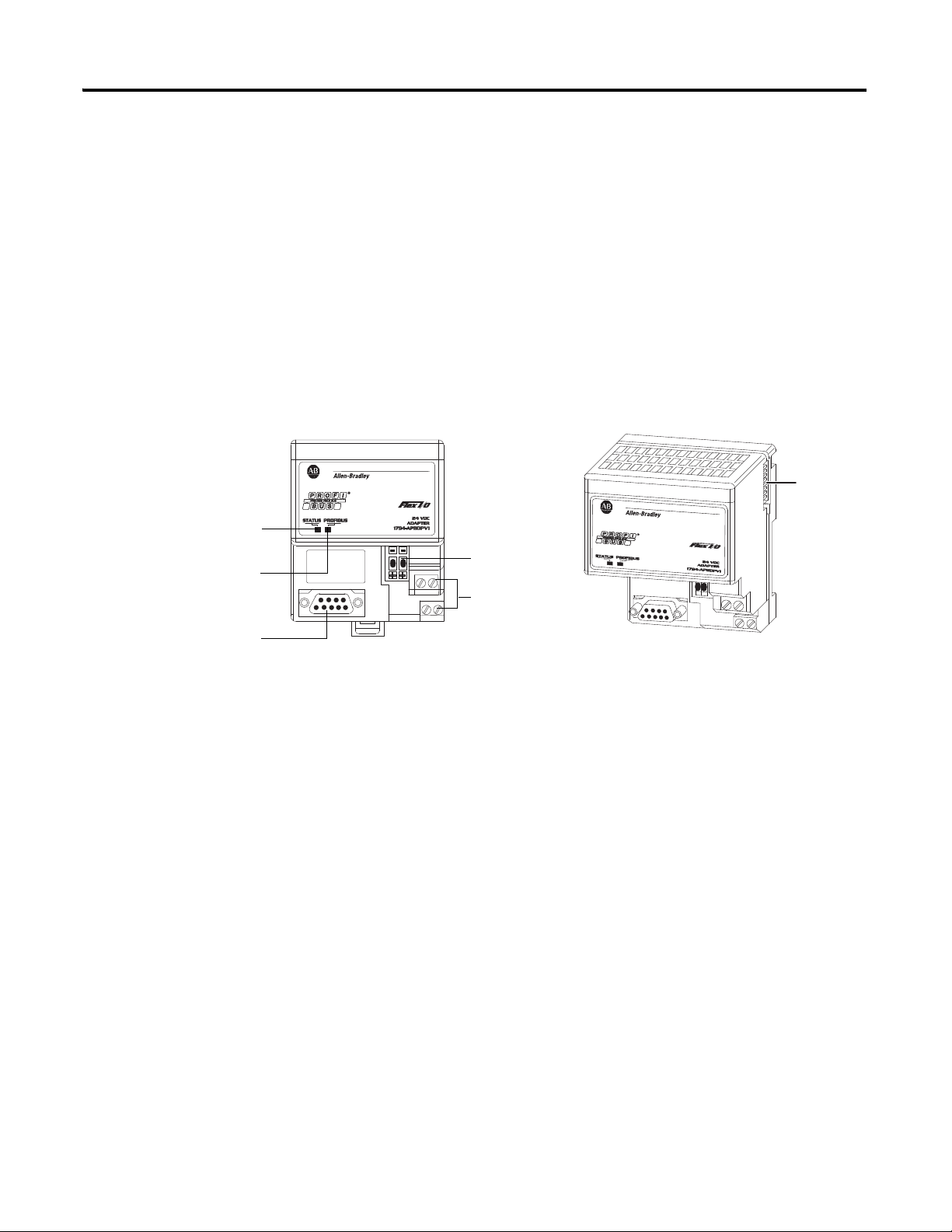
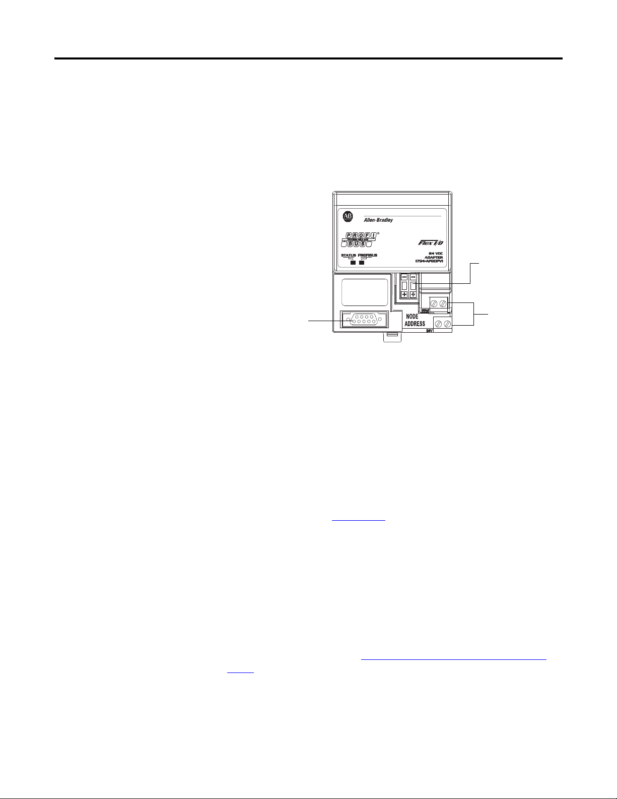
Overview of the FLEX I/O PROFIBUS APBDPV1 Module 3
1119 1120
Status indicator
(green/red)
PROFIBUS indicator
(green/red)
PROFIBUS DP
network
connector
FlexBus
connector
24V DC wiring
connection
terminals
Node address
switches
Bandwidth and Range
The FLEX I/O PROFIBUS APB adapter baud-rate is now 12 MBd and,
although the physically PROFIBUS address range is still limited to 1..99, the
logical address range is 1..126.
PROFIBUS APBDPV1 Adapter Components
The adapter module consists of the following components:
• two diagnostic indicators
•PROFIBUS DP network connector
• 24V DC power wiring connection terminals
• two node address switches
Diagnostic Indicators
Diagnostic indicators are located on the front panel of the adapter module. They
show both normal operation and error conditions in your FLEX I/O system. The
indicators are:
• Device status (STATUS)
• Communication link status (PROFIBUS)
Upon power-up, the adapter goes to an initialization state and performs a self-test
(memory check, data memory clear, CRC on code). The indicators also go
through a self-test sequence. If a failure occurs, the adapter transitions to a faulted
state and waits for reset (cycle power). Otherwise, the adapter begins monitoring
the network (run state) for messages.
Network Connector
Use the 9-pin SUB-D connector to connect your adapter to the PROFIBUS
network.
Publication 1794-UM064B-EN-P - May 2014
Page 16
4 Overview of the FLEX I/O PROFIBUS APBDPV1 Module
99
44560
PROFIBUS
DP Network Connector
(9-pin SUB-D)
24V DC wiring
connection
terminals
Thumbwheel
switches for setting
the node address
Set the Node Address Switches
Set the thumbwheel switches to 00 to allow node addressing by software
configuration tool to set the range from 1…125. Address changes take effect only
after cycling power. Use a pen to press either the + or – buttons to change the
number.
Mount and Remove Your System
Power Wiring
Connection terminals are provided for connecting the required 24V DC power
to the front of the module. The power wiring can be daisy-chained to the
terminal base unit located next to the adapter to supply power to the module
installed in that base unit.
Refer to the FLEX I/O PROFIBUS Communications Adapter Installation
Instructions, publication 1794-IN114
learn how to install and wire the adapter.
You can horizontally or vertically mount the FLEX I/O system on a standard
DIN rail. The adapter and terminal base easily snap on the DIN rail by hand.
Refer to the installation instructions shipped with these components.
Screw holes are also provided to horizontally or vertically panel-mount your
system in an enclosure. To panel-mount your FLEX I/O system, use the optional
mounting kit (1794-NM1). See Example of a DIN Rail-Mounted System
page 5.
, that you received with your adapter to
on
Publication 1794-UM064B-EN-P - May 2014
Page 17
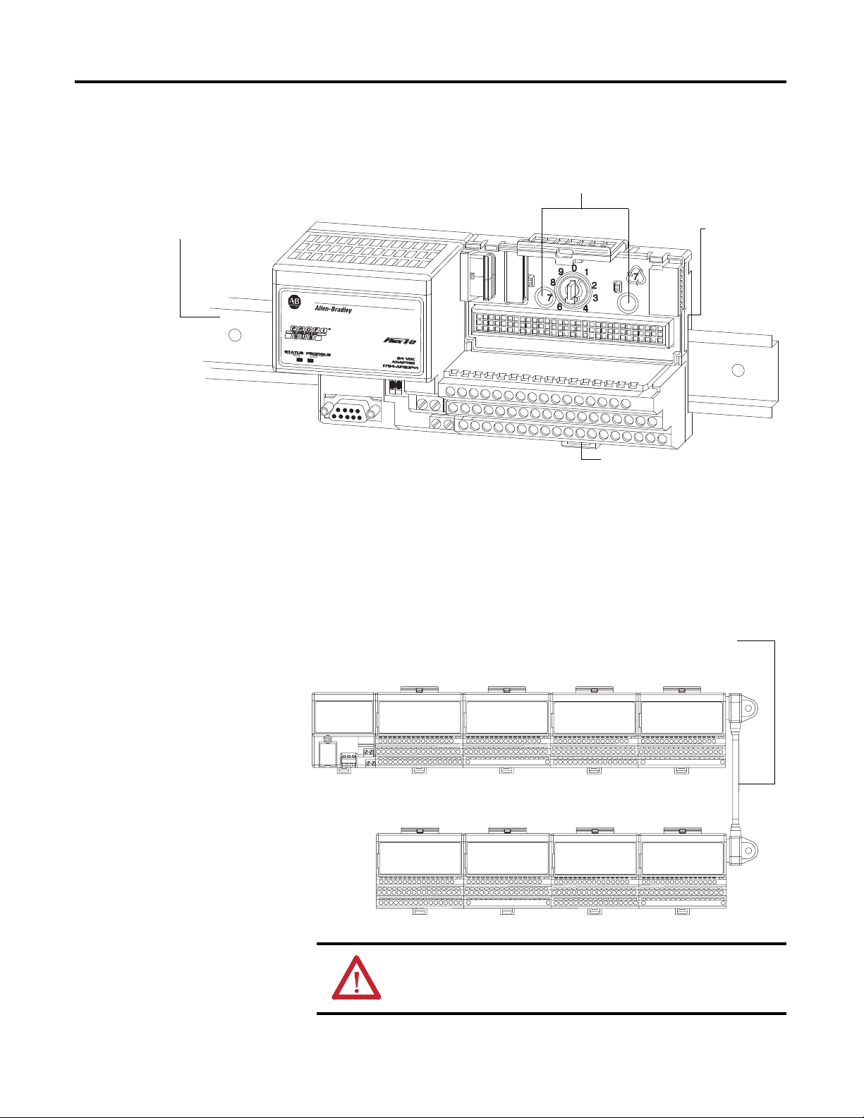
Overview of the FLEX I/O PROFIBUS APBDPV1 Module 5
1114
Screw holes are available for panel-mounting
Locking tab connector holds
terminal base onto DIN rail
DIN rail
Allen Bradley catalog number
199-DR1
DIN 46277-3
EN 50022 (35 X 7.5mm)
Components are
slotted to accept
a DIN rail
1115
1794-CE1 or 1794-CE3
extender cable
Example of a DIN Rail-Mounted System
Optional Accessories
Extender Cables (1794-CE1 or -CE3)
Use the optional 1794-CE1, 0.3m (11.81 in.) or -CE3, 0.9m (35.43 in.) extender
cable (one per system) to arrange your system in two rows or split your system
into horizontal and vertical orientation.
ATTENTION: Do not use more than one extender cable per system
Publication 1794-UM064B-EN-P - May 2014
Page 18

6 Overview of the FLEX I/O PROFIBUS APBDPV1 Module
1116
1794-NM1
Mounting Kit with
18 screws (2 screws for
the adapter and 2 screws
for each module
Mounting Kit (1794-NM1)
Use the optional 1794-NM1 mounting kit to mount your system on a panel or
wall without a DIN rail.
Publication 1794-UM064B-EN-P - May 2014
Page 19
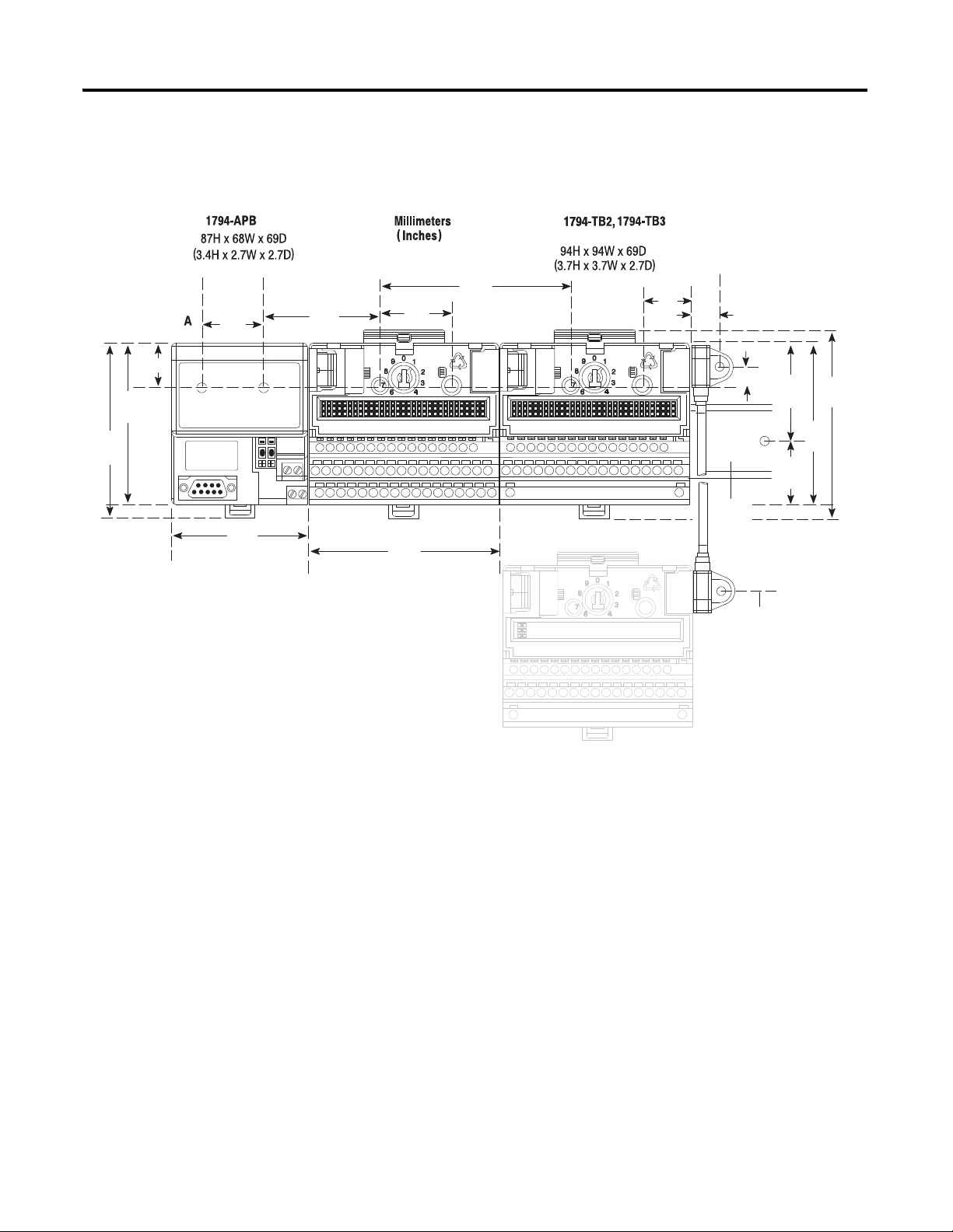
Mounting Dimensions and
Optional
mounting
kit
35
(1.4)
21 (0.83)
35
(1.4)
94
(3.7)
23
(0.9)
17
(0.6)
8
(0.3)
50
(2.0)
30
(1.2)
DIN
Rail
80
(3.2)
80
(3.2)
87
(3.4)
68
(2.7)
94
(3.7)
94
(3.7)
59
(2.3)
For 1794-CE1
Approximately 292.1 (11.5)
from upper connector.
For 1794-CE3
Approximately 901 (35.5)
from upper connector.
DPV1
1117
Spacing Requirements
Overview of the FLEX I/O PROFIBUS APBDPV1 Module 7
Chapter Summary
In this chapter you learned about the FLEX I/O PROFIBUS APBDPV1 adapter
module and the FLEX I/O system. Read the next chapter to learn how to
communicate with your module.
Publication 1794-UM064B-EN-P - May 2014
Page 20

8 Overview of the FLEX I/O PROFIBUS APBDPV1 Module
Notes:
Publication 1794-UM064B-EN-P - May 2014
Page 21
Communicate With Your Module
PROFIBUS
Adapter
Read
Read
Words
Inputs
Status
Outputs
Configuration
Inputs
Status
Outputs
Configuration
Inputs
Status
Outputs
Configuration
Write
Words
15
0
Write
1122
Chapter
2
Overview
Communication Over the I/O Backplane
Read this chapter to familiarize yourself with configurable features on the input
and output analog modules
For Information About See Page
Communication Over the I/O Backplane 9
Polled I/O Structure 10
Map Data into the Image Table 12
Defaults 68
One 1794-APBDPV1 PROFIBUS adapter can interface with up to eight
terminal base units with installed FLEX I/O modules, forming a FLEX I/O
system of up to eight slots. The adapter communicates to other network system
components over the PROFIBUS network. The adapter communicates with its
I/O modules over the backplane.
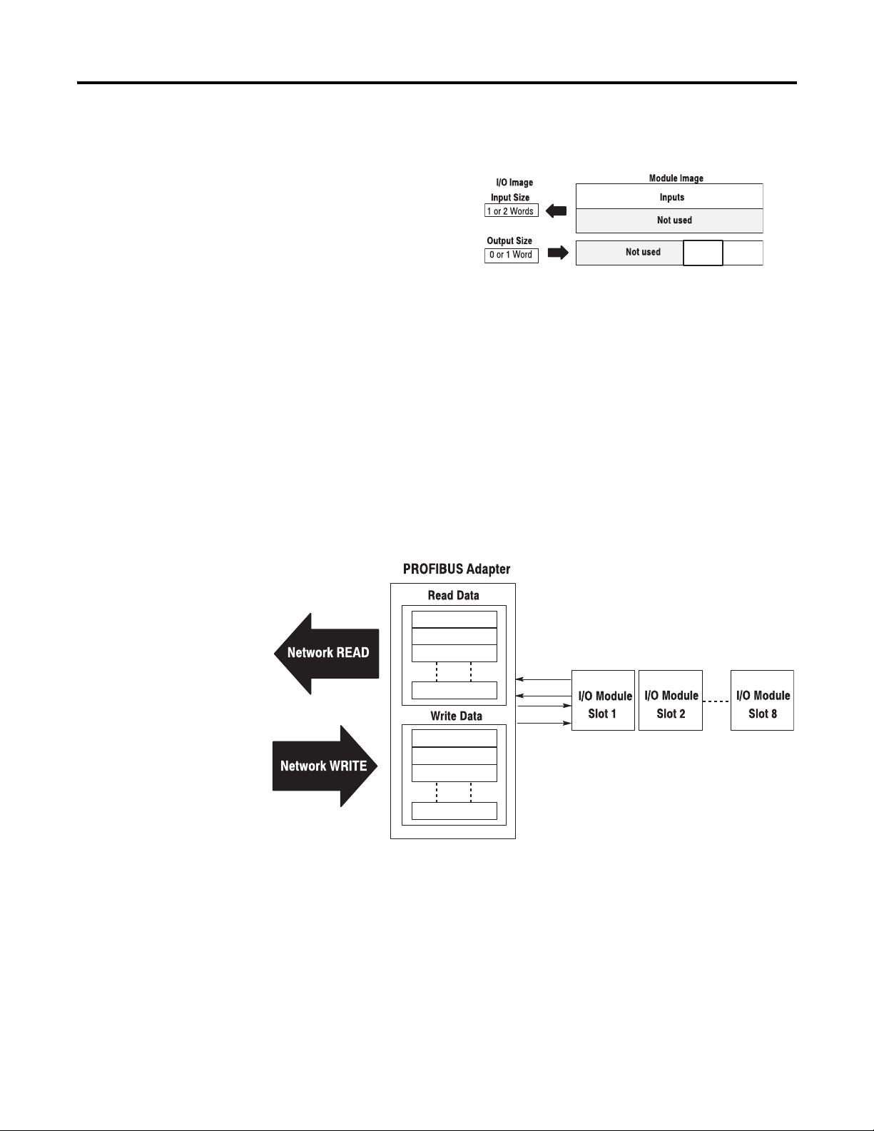
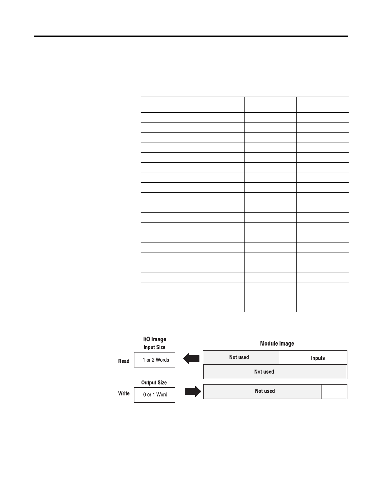
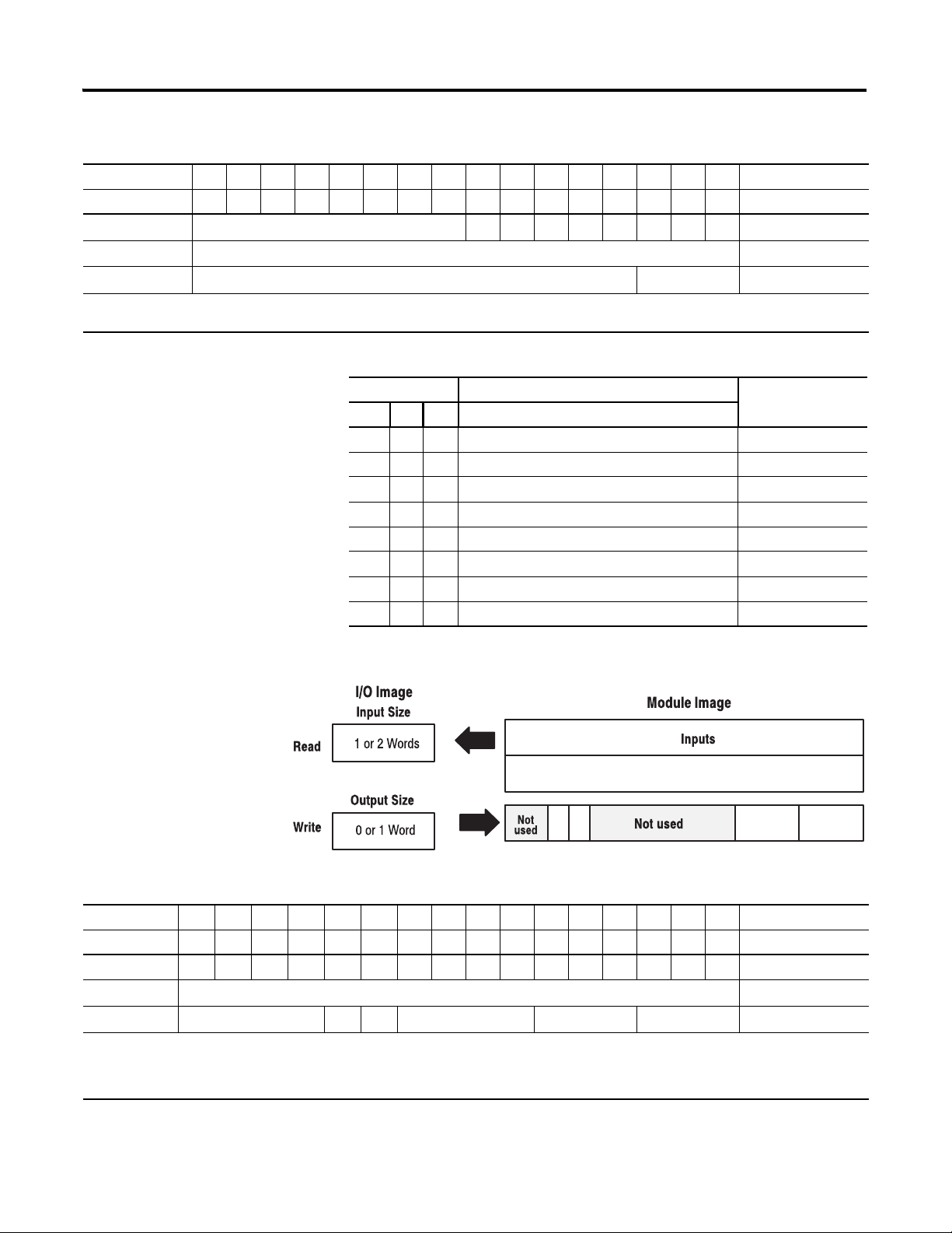
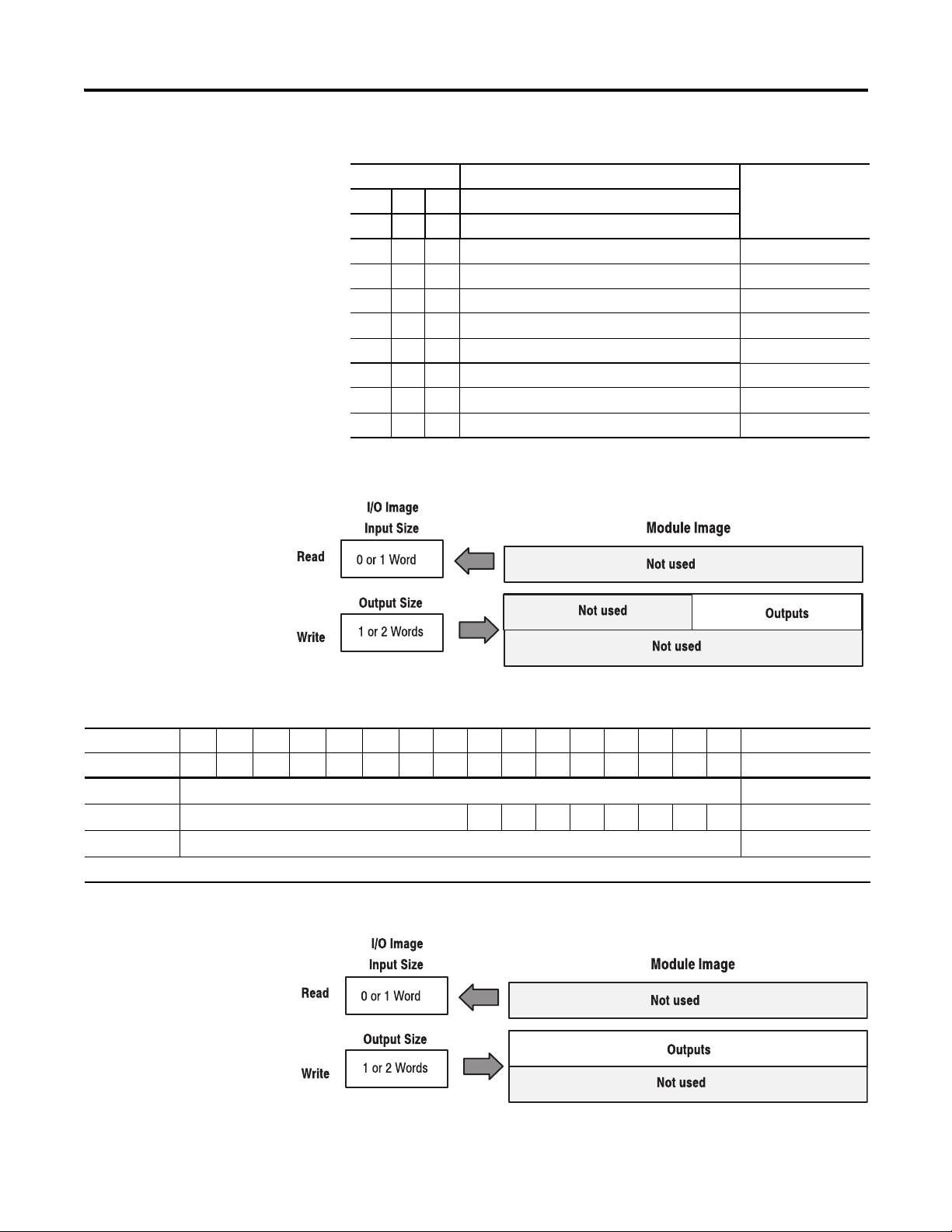
The I/O map for a module is divided into read words and write words. Read
words consist of input and status words, and write words consist of output and
configuration words. The number of read words or write words can be 0 or more.
The length of each I/O module’s read words and write words vary in size
depending on module complexity. Each I/O module will support at least 1 input
word or 1 output word. Status and configuration are optional, depending on
the module.
Page 22
10 Communicate With Your Module
Delay
Time
Delay
Time
1123
16-point Discrete Input Module
Adapter Status
Read
Write
Slot 1 Input Data
Slot 2 Input Data
Slot 8 Input Data
Adapter Status
Slot 1 Output Data
Slot 2 Output Data
Slot 8 Output Data
1124
For example, a 16 point discrete input module will have up to 2 read words and 1
write word.
Refer to each module user manual I/O map for the exact mapping.
Polled I/O Structure
The first word of output data received by the adapter is the Adapter Status Word.
Output data is received by the adapter in the order of the installed I/O modules.
The Output data for Slot 1 is received first, followed by the Output data for
Slot 2, and so on up to slot 8. All bits in the output status word are reserved.
The first word of input data sent by the adapter is the Adapter Status Word. This
is followed by the input data from each slot, in the order of the installed I/O
modules. The Input data from Slot 1 is first after the status word, followed by
Input data from Slot 2, and so on up to slot 8.
Publication 1794-UM064B-EN-P - May 2014
Adapter Input Status Word
The input status word consists of:
• I/O module fault bits — 1 status bit for each slot
Page 23

• node address changed — 1 bit
1125
I/O Module Fault Bits
Bit: 15 014 13 12 11 10 9 8 7 6 5 4 3 2 1
Communicate With Your Module 11
Slot 8
Slot 7
Slot 6
Slot 5
Slot 1
Slot 2
Slot 3
Slot 4
Node Address Changed Bit
Reserved
The adapter input status word bit descriptions are shown in Ta b l e
Wor d B it s.
Input Status Word Bits
Bit Description Bit Explanation
I/O Module Fault
Reserved 1…7 Reserved
Node Address
changed
8 This bit is set (1) when an error is detected in slot position 1.
9 This bit is set (1) when an error is detected in slot position 2.
10 This bit is set (1) when an error is detected in slot position 3.
11 This bit is set (1) when an error is detected in slot position 4.
12 This bit is set (1) when an error is detected in slot position 5.
13 This bit is set (1) when an error is detected in slot position 6.
14 This bit is set (1) when an error is detected in slot position 7.
15 This bit is set (1) when an error is detected in slot position 8.
0 This bit is set (1) when the node address switch setting has been
changed since power up.
Input Status
Possible causes for an I/O module fault are:
• transmission errors on the FLEX I/O backplane
• a failed module
• a module removed from its terminal base
• an incorrect module inserted in a slot position
• an empty slot
The node address changed bit is set when the node address switch setting has
been changed since power up. The new node address does not take effect until
the adapter has been powered down and then powered back up. Until this power
cycling occurs, the node address switches will not match the actual node address.
Publication 1794-UM064B-EN-P - May 2014
Page 24
12 Communicate With Your Module
Filter
Time
1126
Map Data into the Image Table
Commonly used FLEX I/O modules used with the PROFIBUS adapter are
listed below. A full list of modules is available in the GSD file. For more
information on the GSD file, see Device Data Base (GSD) File
FLEX I/O Data Mapping Tables
Module Description Catalog Number For image table
8 Sink input module 1794-IB8 12
16 Sink input module 1794-IB16 13
8 Source output module 1794-OB8 14
16 Source output module 1794-OB16 14
16 Source input module 1794-IV16 15
16 Sink output module 1794-OV16 16
8 Electronically fused output module 1794-OB8EP 16
10 input/6 output module 1794-IB10XOB6 17
8 input module 1794-IA8 18
8 output module 1794-OA8 19
8 relay output module 1794-OW8 19
8 input analog module 1794-IE8 20
4 output analog module 1794-OE4 23
4 in/2 out analog combo module 1794-IE4XOE2 25
8 input RTD analog module 1794-IR8 28
8 input thermocouple module 1794-IT8 32
8 input thermocouple/RTD/mV module 1794-IRT8 36
2 input pulse counter module 1794-ID2 59
4 input encoder counter module 1794-IP4 63
SCANport module 1203-FM1 66
in Appendix B.
mapping see page
Publication 1794-UM064B-EN-P - May 2014
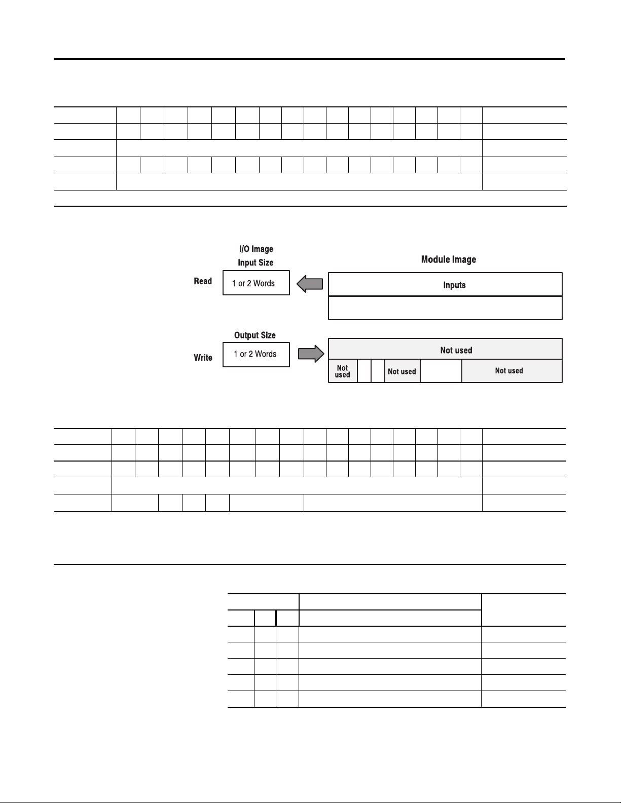
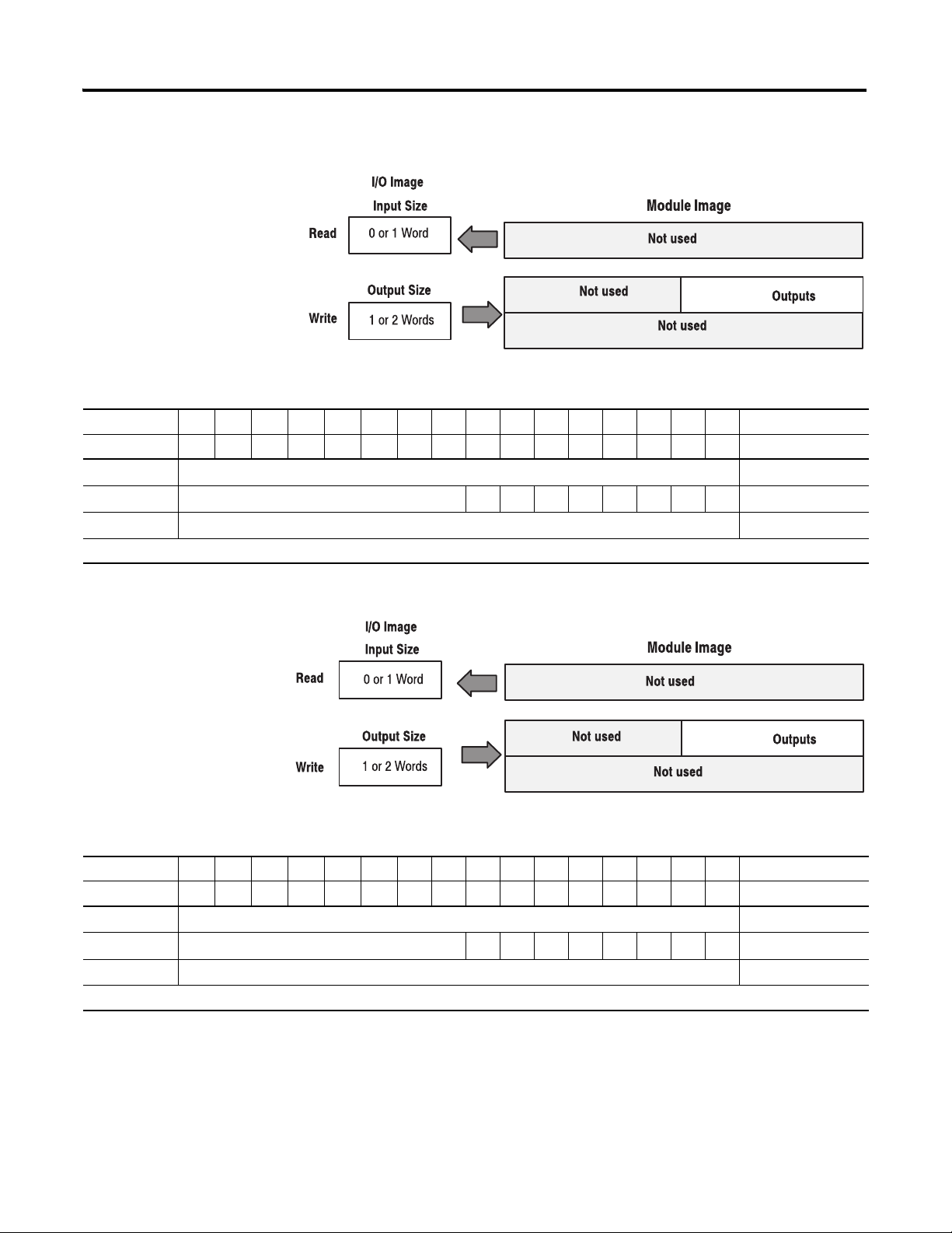
1794-IB8 — 8 Point Digital Input Module Image Table Mapping
Page 25
Communicate With Your Module 13
1127
1794-IB8 Memory Map
Decimal Bit 15141312111009080706050403020100Size
Octal Bit 17161514131211100706050403020100Read Words
Not used
Not used
Not used
D7 D6 D5 D4 D3 D2 D1 D0 Read Word 0
Read Word 1
FT 00…07 Write Word 0
Where: D = Input Data (D0 corresponds to input 0, D1 corresponds to input 1, and so on)
DT = Input Filter Time (FT 00…07 corresponds to inputs 0…7)
1794-IB8 Input Filter Times
Description Selected
02 01 00 Filter Time for Inputs 00…07
Filter Time
0 0 0 Filter Time 0 (default) 0.256 ms
0 0 1 Filter Time 1 0.512 ms
0 1 0 Filter Time 2 1 ms
0 1 1 Filter Time 3 2 ms
1 0 0 Filter Time 4 4 ms
1 0 1 Filter Time 5 8 ms
1 1 0 Filter Time 6 16 ms
1 1 1 Filter Time 7 32 ms
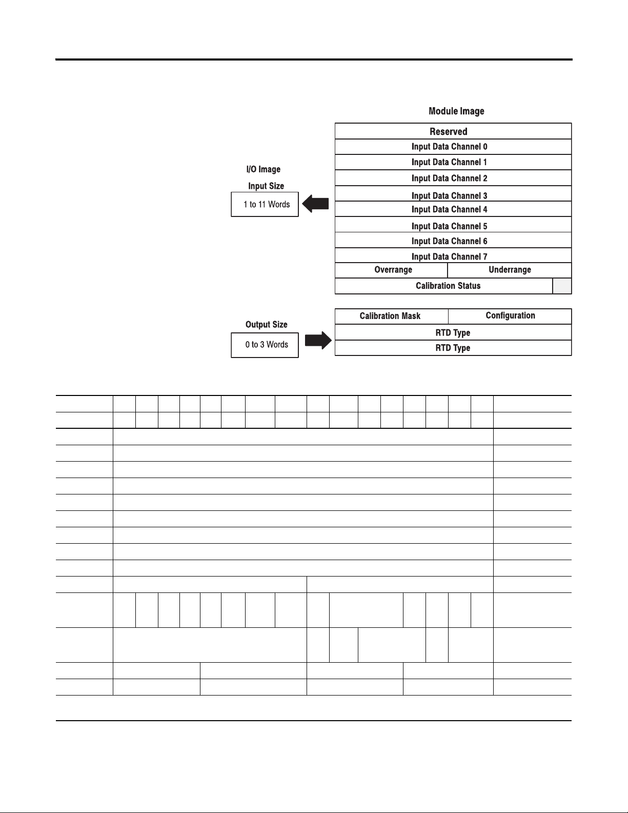
1794-IB16 – 16-point Digital Input Module Image Table Mapping
Counter
RCDF
Filter
Tim e
Filter
Time
1794-IB16 Memory Map
Decimal Bit 15 14 13 12 1110 09080706050403020100Size
Octal Bit 17 16 15 14 1312 11100706050403020100Read Words
D15 D14 D13 D12 D11 D10 D9 D8 D7 D6 D5 D4 D3 D2 D1 D0 Read Word 0
Counter
Not used
Where: D = Input Data (D0 corresponds to input 0, D1 corresponds to input 1, and so on)
DT = Input Filter Time (FT 00…11 corresponds to inputs 0…11; FT 12…15 corresponds to inputs 12…15)
DF = Disable Filter
RC = Reset Counter
DF RC FT 12…15 FT 00…07 Write Word 0
Publication 1794-UM064B-EN-P - May 2014
Read Word 1
Page 26
14 Communicate With Your Module
1128
1130
1794-IB16 Input Delay Times
Description Selected
02 01 00 Filter Time for Inputs 00…11
Filter Time
05 04 03 Filter Time for Inputs 12…15
0 0 0 Filter Time 0 (default) 0.256 ms
0 0 1 Filter Time 1 0.512 ms
0 1 0 Filter Time 2 1 ms
0 1 1 Filter Time 3 2 ms
1 0 0 Filter Time 4 4 ms
1 0 1 Filter Time 5 8 ms
1 1 0 Filter Time 6 16 ms
1 1 1 Filter Time 7 32 ms
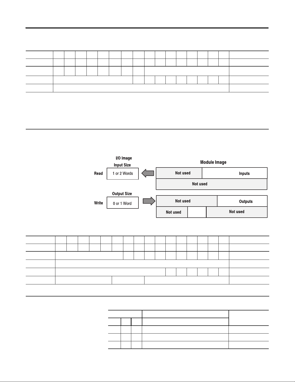
1794-OB8 – 8 Point Discrete Output Module Image Table Mapping
1794-OB8 Memory Map
Decimal Bit 15 14 1312 11 1009080706050403020100Size
Octal Bit 17 16 15 14 13 12 11 10 07 06 05 04 03 02 01 00 Read Words
Not used
Not used
O7 O6 O5 O4 O3 O2 O1 O0 Write Word 0
Not used
Where: O = Output value (O0 corresponds to output 0, O1 corresponds to output 1, and so on)
1794-OB16 – 16-point Discrete Output Module Image Table Mapping
Read Word 0
Write Word 1
Publication 1794-UM064B-EN-P - May 2014
Page 27
Communicate With Your Module 15
1132
1794-OB16 Memory Map
Decimal Bit 15 14 13 12 1110 09080706050403020100Size
Octal Bit 17 16 15 14 1312 11100706050403020100Read/Write Words
Not used
O15 O14 O13 O12 O11 O10 O9 O8 O7 O6 O5 O4 O3 O2 O1 O0 Write Word 0
Not used
Where: O = Output value (O0 corresponds to output 0, O1 corresponds to output 1, and so on)
Read Word 0
Write Word 1
1794-IV16 – 16-point Source Input Module Image Table Mapping
Counter
RCDF
FT for all
Channels
1794-IV16 Memory Map
Decimal Bit15 14 1312 1110 09 08 0706050403020100Size
Octal Bit 1716 1514 13 12 11 10 0706050403020100Read/Write Words
D15 D14 D13 D12 D11 D10 D9 D8 D7 D6 D5 D4 D3 D2 D1 D0 Read Word 0
Counter
Not used
Where: D = Input Data (D0 corresponds to input 0, D1 corresponds to input 1, and so on)
DT = Input Filter Time (FT 00…11 corresponds to inputs 0…11; FT 12…15 corresponds to inputs 12…15)
DF = Disable Filter
RC = Reset Counter
NU = Not Used
DF RC NU FT for all channels
Not used
Read Word 1
Write Word 0
1794-IV16 Input Filter Times
Description Selected
10 09 08 Filter Time for Inputs 00-15 (00…17)
0 0 0 Filter Time 0 (default) 216 µs
0 0 1 Filter Time 1 512 µs
0 1 0 Filter Time 2 1 ms
0 1 1 Filter Time 3 2 ms
1 0 0 Filter Time 4 4 ms
Publication 1794-UM064B-EN-P - May 2014
Filter Time
Page 28
16 Communicate With Your Module
1134
1136
1794-IV16 Input Filter Times
Description Selected
10 09 08 Filter Time for Inputs 00-15 (00…17)
Filter Time
1 0 1 Filter Time 5 8 ms
1 1 0 Filter Time 6 16 ms
1 1 1 Filter Time 7 32 ms
1794-OV16 – 16-point Sink Output Module Image Table Mapping
1794-OV16 Memory Map
Decimal Bit 15 14 1312 11 1009080706050403020100Size
Octal Bit 17 16 15 14 13 12 11 10 07 06 05 04 03 02 01 00 Read/Write Words
Not used
O15 O14 O13 O12 O11 O10 O9 O8 O7 O6 O5 O4 O3 O2 O1 O0 Write Word 0
Not used
Where: O = Output value
Read Word 0
Write Word 1
Publication 1794-UM064B-EN-P - May 2014
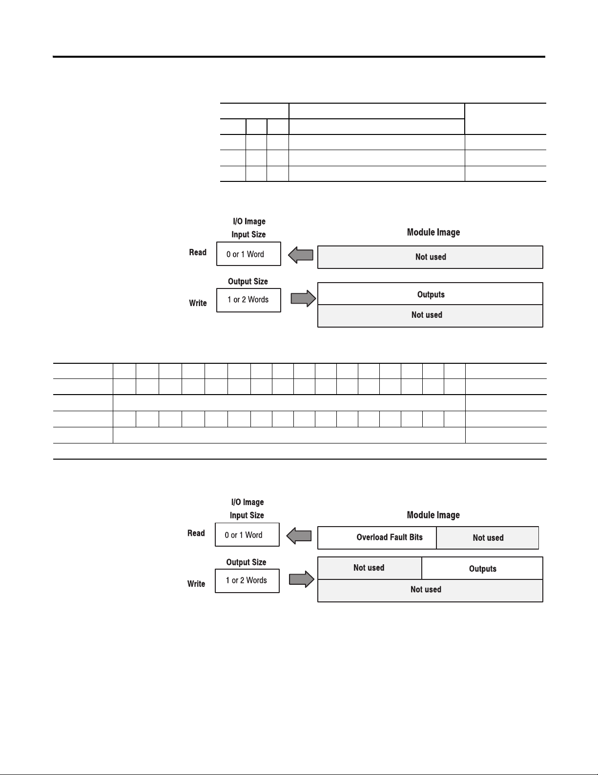
1794-OB8EP – 8-point Discrete Protected Output Module Image Table Mapping
Page 29
Communicate With Your Module 17
Filter
Time
1137
1794-OB8EP Memory Map
Decimal Bit15 14 1312 1110 09 08 0706050403020100Size
Octal Bit 1716 1514 13 12 11 10 0706050403020100Read/Write Words
F7 F6 F5 F4 F3 F2 F1 F0
Not used
FR
Reserved
O7
Reserved
Where: F = overload fault bits – 1 = fault present; 0 = no fault
Using the Fault Reset Button When you press the manual reset button:
1. The fault indicator for the faulted output turns off for about 1.2 s (the faulted output will not attempt to turn on during this delay)
2. After the 1.2 s delay, the faulted output attempts to turn on
3. If the external condition causing the fault is corrected, the output remains on, the fault indicator is off, and the status indicator is on
(1)
The unused lower byte in read word 1 floats during operation. Do not use this byte for fault status.
Ox = Output Data (O0 corresponds to output 0, O1 corresponds to output 1, and so on)
FR = fault reset bit – 1 = reset output; 0 = no change.
(1)
Read Word 0
O6 O5 O4 O3 O2 O1 O0 Write Word 0
Write Word 1
1794-IB10XOB6 – 16-point Digital Input/Output Module Image Table Mapping
1794-IB10XOB6 Memory Map
Decimal Bit 15 14 13 12 1110 09080706050403020100Size
Octal Bit 17 16 15 14 1312 11100706050403020100Read/Write Words
Not used
Not used
Not used
Not used
Where: I = Input Channel
O = Output Channel
I9 I8 I7 I6 I5 I4 I3 I2 I1 I0 Read Word 0
Read Word 1
O5 O4 O3 O2 O1 O0 Write Word 0
Filter Time Not used Write Word 1
1794-IB10XOB6 Input Filter Times
Description Selected
02 01 00 Filter Time for Inputs 00…07
0 0 0 Filter Time 0 (default) 0.256 ms
0 0 1 Filter Time 1 0.512 ms
0 1 0 Filter Time 2 1 ms
Publication 1794-UM064B-EN-P - May 2014
Filter Time
Page 30
18 Communicate With Your Module
1138
1794-IB10XOB6 Input Filter Times
Description Selected
02 01 00 Filter Time for Inputs 00…07
Filter Time
0 1 1 Filter Time 3 2 ms
1 0 0 Filter Time 4 4 ms
1 0 1 Filter Time 5 8 ms
1 1 0 Filter Time 6 16 ms
1 1 1 Filter Time 7 32 ms
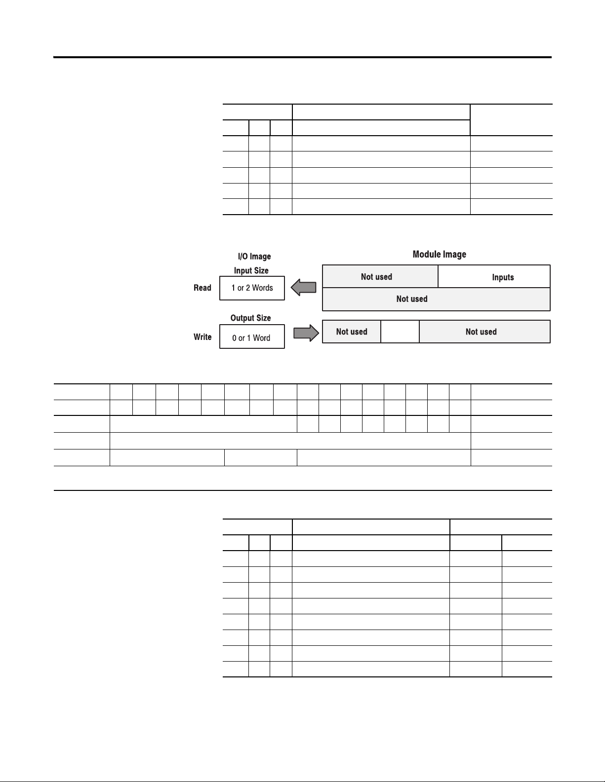
1794-IA8 – 8-point Discrete Input Module Image Table Mapping
Filter
Tim e
1794-IA8 Memory Map
Decimal Bit15 14 1312 1110 09 08 0706050403020100Size
Octal Bit 17 16 15 14 13 12 11 10 07 06 05 04 03 02 01 00 Read/Write Words
Not used
Not used
Not used
Where: D = Input Data (D0 corresponds to input 0, D1 corresponds to input 1,and so on)
FT = Input Filter Time (FT 00…07 corresponds to inputs 0…7)
FT 00…07 Not used Write Word 0
D7 D6 D5 D4 D3 D2 D1 D0 Read Word 0
Read Word 1
Publication 1794-UM064B-EN-P - May 2014
1794-IA8 Input Filter Times
Bits Description Maximum Filter Time
02 01 00 Filter Time for Inputs 00…15 (00…17) Off to On On to Off
0 0 0 Filter Time 0 (default) 8.6 ms 26.6 ms
0 0 1 Filter Time 1 9 ms 27 ms
0 1 0 Filter Time 2 10 ms 28 ms
0 1 1 Filter Time 3 12 ms 30 ms
1 0 0 Filter Time 4 17 ms 35 ms
1 0 1 Filter Time 5 26 ms 44 ms
1 1 0 Filter Time 6 43 ms 61 ms
1 1 1 Filter Time 7 78 ms 96 ms
Page 31
Communicate With Your Module 19
1139
1140
1794-OA8 – 8-point Discrete Output Module Image Table Mapping
1794-OA8 Memory Map
Decimal Bit 15 14 13 12 1110 09080706050403020100Size
Octal Bit 17 16 15 14 1312 11100706050403020100Read Words
Not used
Not used
O7 O6 O5 O4 O3 O2 O1 O0 Write Word 0
Not used
Where: O = Output value (O0 corresponds to output 0, O1 corresponds to output 1, and so on)
1794-OW8 – 8-point Discrete Relay Output Module Image Table Mapping
Read Word 0
Write Word 1
1794-OW8 Memory Map
Decimal Bit 15 14 13 12 1110 09080706050403020100Size
Octal Bit 17 16 15 14 1312 11100706050403020100Read/Write Words
Not used
Not used
O7 O6 O5 O4 O3 O2 O1 O0 Write Word 0
Not used
Where: O = Output value (O0 corresponds to output 0, O1 corresponds to output 1, and so on)
Publication 1794-UM064B-EN-P - May 2014
Read Word 0
Write Word 1
Page 32

20 Communicate With Your Module
1141
1794-IE8 Series B – 8 Input Analog Module Image Table Mapping
1794-IE8/B Memory Map
Decimal Bit 15 14 1312 11 1009080706050403020100Size
Octal Bit 17 16 15 14 13 12 11 10 07 06 05 04 03 02 01 00 Read/Write Words
S Analog Value Channel 0
S Analog Value Channel 1
S Analog Value Channel 2
S Analog Value Channel 3
S Analog Value Channel 4
S Analog Value Channel 5
S Analog Value Channel 6
S Analog Value Channel 7
PU Not used – set to zero
C6 C5 C4 C3 C2 C1 C0 F7 F6 F5 F4 F3 F2 F1 F0 Write Word 0
C7
Not used
Where: PU = Power up bit – included in series B modules only.
U = Underrange bits for 4…20 mA inputs
C = Configure select bit
F = Full range bit
S = sign bit (in 2’s complement)
U7 U6 U5 U4 U3 U2 U1 U0 Read Word 8
Read Word 0
Read Word 1
Read Word 2
Read Word 3
Read Word 4
Read Word 5
Read Word 6
Read Word 7
Write Word 1…5
Publication 1794-UM064B-EN-P - May 2014
Page 33

Communicate With Your Module 21
1794-IE8/B Range Selection Bits
Channel No. Channel 0 Channel 1 Channel 2 Channel 3 Channel 4 Channel 5 Channel 6 Channel 7
F0 C0 F1 C1 F2 C2 F3 C3 F4 C4 F5 C5 F6 C6 F7 C7
Decimal Bits
(Octal Bits)
0…10V DC/0…20 mA
4…20 mA
-10…10V DC
Off
Where: C = Configure select bit
00 08
1010101010101010
0101010101010101
1111111111111111
0000000000000000
F = Full range bit
Off = When configured to off, individual channels will return 0000H on Series B modules, and 4…20 mA on Series A modules.
(10)
01 09
(11)
02 10
(12)
03 11
(13)
04 12
(14)
04 13
(15)
06 14
(16)
07 15
1794-IE8 Word/Bit Descriptions
Word Decimal Bit Definition
Read Word 0 Bits 00…14 Channel 0 analog data – 12-bit left justified two’s complement number;
Bit 15 Channel 0 analog data sign bit.
Read Word 1 Bits 00…14 Channel 1 analog data – 12-bit left justified two’s complement number;
Bit 15 Channel 1 analog data sign bit.
Read Word 2 Bits 00…14 Channel 2 analog data – 12-bit left justified two’s complement number;
Bit 15 Channel 2 analog data sign bit.
Read Word 3 Bits 00…14 Channel 3 analog data – 12-bit left justified two’s complement number;
Bit 15 Channel 3 analog data sign bit.
Read Word 4 Bits 00…14 Channel 4 analog data – 12-bit left justified two’s complement number;
Bit 15 Channel 4 analog data sign bit.
Read Word 5 Bits 00…14 Channel 5 analog data – 12-bit left justified two’s complement number;
Bit 15 Channel 5 analog data sign bit.
Read Word 6 Bits 00…14 Channel 6 analog data – 12-bit left justified two’s complement number;
Bit 15 Channel 6 analog data sign bit.
Read Word 7 Bits 00…14 Channel 7 analog data – 12-bit left justified two’s complement number;
Bit 15 Channel 7 analog data sign bit.
unused lower bits are zero; 4…20 mA uses all 16 bits.
unused lower bits are zero; 4…20 mA uses all 16 bits.
unused lower bits are zero; 4…20 mA uses all 16 bits.
unused lower bits are zero; 4…20 mA uses all 16 bits.
unused lower bits are zero; 4…20 mA uses all 16 bits.
unused lower bits are zero; 4…20 mA uses all 16 bits.
unused lower bits are zero; 4…20 mA uses all 16 bits.
unused lower bits are zero; 4…20 mA uses all 16 bits.
(17)
Publication 1794-UM064B-EN-P - May 2014
Page 34

22 Communicate With Your Module
1794-IE8 Word/Bit Descriptions
Word Decimal Bit Definition
Read Word 8 Bits 00…07 Underrange bits (U) for individual channels (4...20 mA current input only) –
Bit 00 corresponds to input channel 0, bit 01 corresponds to input channel
1, and so on. When set (1), indicates either a broken or open input wire, or
input current below 4.20 mA.
Bits 08…14 Not used – set to 0.
Bit 15 Power up bit – included in Series B modules only. This bit is 0 in series A
modules. This bit is set to 1 when all bits in the configuration register are 0
(unconfigured state). The configuration register can be cleared by either of
the reset inputs, or by the user writing all zeroes to it.
Write Word 0 Bits 00…07 Full range bits (F) for individual channels – Bit 00 corresponds to input
channel 0, bit 01 corresponds to input channel 1, and so on. Refer to range
selection table.
Bits 08…15 Configure select bits (C) for individual channels – Bit 08 corresponds to
input channel 0, bit 09 corresponds to input channel 1, and so on. Refer to
range selection table.
Write Word 1 Bits 00…15 Not used – set to 0
Write Word 2 Bits 00…15 Not used – set to 0
Write Word 3 Bits 00…15 Not used – set to 0
Write Word 4 Bits 00…15 Not used – set to 0
Write Word 5 Bits 00…15 Not used – set to 0
Publication 1794-UM064B-EN-P - May 2014
Page 35

Communicate With Your Module 23
Chx SS Config
1142
1794-OE4 Series B – 4 Output Analog Module Image Table Mapping
1794-OE4/B Memory Map
Decimal Bit15 14 13 12 11 1009080706050403020100Size
Octal Bit 17 16 15 14 13 12 11 10 07 06 05 04 03 02 01 00 Read/Write Words
S Not used – set to zero W3 W2 W1 W0 Read Word 0
S Analog Value Channel 0 Write Word 0
S Analog Value Channel 1 Word 1
S Analog Value Channel 2 Word 2
S Analog Value Channel 3 Word 3
S Not used – set to 0 Chx Safe State Config Word 4
PU Not used – set to 0 C3 C2 C1 C0 Not used – set to 0 F3 F2 F1 F0 Word 5
S Not used – set to 0 Word 6…9
Where: PU = Power up bit – included in Series B modules only.
W = Diagnostic bits for current output wire broken or load resistance high. (Not used on voltage outputs.)
S = Sign bit (in 2’s complement)
C = Configure select bit
F = Full range bit
1794-OE4/B Range Selection Bits (Write Word 6)
Channel No. Channel 0 Channel 1 Channel 2 Channel 3
F0 C0 F1 C1 F2 C2 F3 C3
Decimal Bits
(Octal Bits)
4…20 mA 10101010
0…10V DC/0…20 mA01010101
00 08 01 09 02 10 03 11
Publication 1794-UM064B-EN-P - May 2014
Page 36

24 Communicate With Your Module
1794-OE4/B Range Selection Bits (Write Word 6)
Channel No. Channel 0 Channel 1 Channel 2 Channel 3
F0 C0 F1 C1 F2 C2 F3 C3
Decimal Bits
(Octal Bits)
-10…10V DC 11111111
Off 00000000
Where: C = Configure select bit
00 08 01 09 02 10 03 11
F = Full range bit
Off = When configured to off, individual channels will return 0V.
1794-OE4/B Word/Bit Descriptions
Word Decimal Bit Definition
Read Word 0 Bits 00…03 Current Outputs only – When set (1), the wire on the output is broken or
Bit 04…14
(04…16)
Bits 15 (17) Power Up bit – included in Series B modules only. This bit is 0 in Series A
Write Word 0 Bit 00…14
(00…16)
Bit 15 (17) Channel 0 analog data sign bit.
Write Word 1 Bit 00…14
(00…16)
Bit 15 (17) Channel 1 analog data sign bit.
Write Word 2 Bit 00…14
(00…16)
Bit 15 (17) Channel 2 analog data sign bit.
Write Word 3 Bit 00…14
(00…16)
Bit 15 (17) Channel 3 analog data sign bit.
Write Word 4 Bit 00…03 Chx Safe State Config – for individual channels. These bits control the
Bits 04…15
(04…17)
the load resistance is too high. Bit 00 corresponds to channel 0, bit 01
corresponds to channel 2, and so on.
Not used – set to zero.
modules. This bit is set to 1 when all bits in the configuration register are 0
(unconfigured state). The configuration register can be cleared by either of
the reset inputs, or by the user writing all zeroes to it.
Channel 0 Analog Data – 12-bit left justified two’s complement number;
unused lower bits are zero; 4…20 mA uses all 16 bits.
Channel 1 Analog Data – 12-bit left justified two’s complement number;
unused lower bits are zero; 4…20 mA uses all 16 bits.
Channel 2 Analog Data – 12-bit left justified two’s complement number;
unused lower bits are zero; 4…20 mA uses all 16 bits.
Channel 3 Analog Data – 12-bit left justified two’s complement number;
unused lower bits are zero; 4…20 mA uses all 16 bits.
safe state analog outputs. Bit 00 corresponds to output channel 0, bit 01
corresponds to output channel 1, and so on.
1 = use words 0, 1, 2 or 3 as directed by channel number n
0 = use words 10, 11, 12 or 13 as directed by channel n
When bits 00…03 are all cleared (0) simultaneously by a communication
error or user choice thru the programmable controller program, word 5 full
range and configure select bits are preserved at their last setting.
Not used – set to zero.
Publication 1794-UM064B-EN-P - May 2014
Page 37

Communicate With Your Module 25
1143
1794-OE4/B Word/Bit Descriptions
Word Decimal Bit Definition
Write Word 5 Bits 00…03 Full range bits (F) for individual channels – Bit 00 corresponds to output
Bits 04…07 Not used – set to zero.
Bits 08…11
(10…13)
Bits 12…15
(14…17)
Write Words
6...9
Bits 00…15
(00…17)
channel 0, bit 01 corresponds to output channel 1, and so on.
Configure select bits (C) for individual channels
Not used – set to zero.
Not used – set to zero.
1794-IE4XOE2 Series B – Analog Combo Module Image Table Mapping
Chx SSC
1794-IE4XOE2 Memory Map
Decimal Bit15 14 13 12 11 1009080706050403020100Size
Octal Bit 17 16 15 14 13 12 11 10 07 06 05 04 03 02 01 00 Read/Write Words
S Analog Value Channel 0 Read Word 0
S Analog Value Channel 1 Read Word 1
S Analog Value Channel 2 Read Word 2
S Analog Value Channel 3 Read Word 3
PU Not used – set to 0 W1 W0 U3 U2 U1 U0 Read Word 4
S Analog Data – Output Channel 0 Write Word 0
S Analog Data – Output Channel 1 Write Word 4
Not used – set to 0 Chx SSC Write Word 2
Not used C5 C4 C3 C2 C1 C0 0 0 F5 F4 F3 F2 F1 F0 Write Word 3
Publication 1794-UM064B-EN-P - May 2014
Page 38

26 Communicate With Your Module
1794-IE4XOE2 Memory Map
Decimal Bit15 14 13 12 11 1009080706050403020100Size
Octal Bit 17 16 15 14 13 12 11 10 07 06 05 04 03 02 01 00 Read/Write Words
Not used – set to 0
Not used – set to zero. Write Words 8 and 9
Where: PU = Power up bit – included in Series B modules only.
W = Diagnostic bits for current output wire broken or load resistance high. (Not used on voltage outputs.)
U = Underrange bits for 4…20 mA inputs
S = Sign bit (in 2’s complement)
Chx SSC = Chx Safe State Config
C = Configure select bit
F = Full range bit
1794-IE4XOE2 Range Selection Bits
Channel No. Input
Decimal Bits
(Octal Bits)
4…20 mA 101010101010
0…10V DC/0…20 mA010101010101
-10…10V DC 111111111111
Off 000000000000
Where: C = Configure select bit
Channel 0
F0 C0 F1 C1 F2 C2 F3 C3 F4 C4 F5 C5
00 08
(10)
F = Full range bit
Off = When configured to off, individual channels will return 0V.
Input
Channel 1
01 09
(11)
Input
Channel 2
02 10
(12)
Input
Channel 3
03 11
(13)
Output
Channel 0
04 12
(14)
Output
Channel 1
05 13
(15)
1794-IE4XOE2 Word/Bit Descriptions
Word Decimal Bit Definition
Read Word 0 Bits 00…14
(00…16)
Bit 15 (17) Channel 0 analog date sign bit.
Read Word 1 Bits 00…14
(00…16)
Bit 15 (17) Channel 1 analog date sign bit.
Read Word 2 Bits 00…14
(00…16)
Bit 15 (17) Channel 2 analog data sign bit.
Read Word 3 Bits 00…14
(00…16)
Bit 15 (17) Channel 3 analog data sign bit.
Channel 0 Analog Data – 12-bit left justified two’s complement number;
unused lower bits are zero; 4…20 mA uses all 16 bits.
Channel 1 Analog Data – 12-bit left justified two’s complement number;
unused lower bits are zero; 4...20 mA uses all 16 bits.
Channel 2 Analog Data – 12-bit left justified two’s complement number;
unused lower bits are zero; 4…20 mA uses all 16 bits.
Channel 3 Analog Data – 12-bit left justified two’s complement number;
unused lower bits are zero; 4…20 mA used all 16 bits.
Publication 1794-UM064B-EN-P - May 2014
Page 39

Communicate With Your Module 27
1794-IE4XOE2 Word/Bit Descriptions
Word Decimal Bit Definition
Read Word 4 Bit 00…03 Underrange bits (U) – for individual channels (4...20 mA current inputs only)
Bits 04…05 Wire Off bits (W) – Current outputs only – When set (1), the wire on the
Bits 06…14
(06…16)
Bit 15 (17) Power Up bit – included in Series B modules only. This bit is always 0 in
Write Word 0 Bits 00…14
(00…16)
Bit15
(17)
Write Word 1 Bits 00…14
(00…16)
Bit15
(17)
Write Word 2 Bits 00…01 Chx Safe Sate Config – for individual channels. These bits control the safe
Bits 02…15
(02…17)
Write Word 3 Bits 00…05 Full Range bits (F) for individual channels – Bit 00 corresponds to input
Bits 06…07 Not used – set to 0.
Bit 08…13
(10…15)
Bits 14…15
(16…17)
Write Words
4 and 5
-Bit 00 corresponds to input channel 0, bit 01 corresponds to input channel 1,
and so on. When set (1), indicates either a broken or open input wire, or input
current is @ or below 4 mA.
current output is broken or the load resistance is too high. Bit 00 corresponds to
input channel 0, bit 01 corresponds to input channel 1, and so on.
Not used
Series A modules. This bit is set to 1 when all bits in the configuration register
(write word 3) are 0 (unconfigured state). The configuration register can be
cleared by either a reset, or by the user writing all zeroes to it.
Channel 0 Analog Data – 12-bit left justified two’s complement number;
unused lower bits are zero; 4...20 mA uses all 16 bits.
Channel 0 analog date sign bit.
Channel 1 Analog Data – 12-bit left justified two’s complement number;
unused lower bits are zero; 4...20 mA uses all 16 bits.
Channel 1 analog date sign bit.
state analog outputs. Bit 00 corresponds to output channel 0, bit 01 corresponds
to output channel 1.
1 = use words 0 and 1 (analog value) as directed by channel number n
0 = use words 6 and 7 (safe state analog value) as directed by channel n
When bits 00...01 are cleared (0) simultaneously by a communication error or
user choice through the programmable controller program, word 3 full range
and configure select bits are preserved at their last setting.
Not used – set to 0.
channel 0, bit 01 corresponds to output channel 1, and so on.
Configure Select bits (C) for individual channels – Bit 08 corresponds to input
channel 0, bit 09 (11) corresponds to input channel 1, bit 10 (12) corresponds to
input channel 2, bit 11 (13) corresponds to input channel 3, bit 12 (14)
corresponds to output channel 0, and bit 13 (15) corresponds to output
channel 1. See Table
Not used – set to 0.
Not used – set to 0.
1794-IE4XOE2 Range Selection Bits on page 26.
Publication 1794-UM064B-EN-P - May 2014
Page 40
28 Communicate With Your Module
1144
1794-IR8 Memory Map
1794-IR8 – RTD Input Analog Module Image Table Mapping
Decimal Bit151413121110 09 08 0706 050403020100Size
Octal Bit 17 16 15 14 13 12 11 10 07 06 05 04 03 02 01 00 Read/Write Words
Reserved Read Word 0
Channel 0 Input Data Read Word 1
Channel 1 Input Data Read Word 2
Channel 2 Input Data Read Word 3
Channel 3 Input Data Read Word 4
Channel 4 Input Data Read Word 5
Channel 5 Input Data Read Word 6
Channel 6 Input Data Read Word 7
Channel 7 Input Data Read Word 8
Overrange bits Underrange bits Read Word 9
00000Bad
Cal
Cal
Done
Cal out
of
0 Critical Error bits Pwr Up0 0 0 Read Word 10
Range
8-bit Calibration Mask Cal
Clk
Gain
Notch Frequency Enh MDT Write Word 0
Offset
Cal
RTD 3 Type RTD 2 Type RTD 1 Type RTD 0 Type Write Word 1
RTD 7 Type RTD 6 Type RTD 5 Type RTD 4 Type Write Word 2
Where: Enh = Enhanced
MDT = Module Data Type
Publication 1794-UM064B-EN-P - May 2014
Page 41

Communicate With Your Module 29
1794-IR8 Word/Bit Descriptions
Word Decimal Bit Definition
Read Word 0 00…15 (00…17) Reserved
Read Word 1 00…15 (00…17) Channel 0 Input data
Read Word 2 00…15 (00…17) Channel 1 Input data
Read Word 3 00…15 (00…17) Channel 2 Input data
Read Word 4 00…15 (00…17) Channel 3 Input data
Read Word 5 00…15 (00…17) Channel 4 Input data
Read Word 6 00…15 (00…17) Channel 5 Input data
Read Word 7 00…15 (00…17) Channel 6 Input data
Read Word 8 00…15 (00…17) Channel 7 Input data
Read Word 9 00…07 Underrange bits – these bits are set if the input signal is below the input
08…15 (10…17) Overrrange bits – these bits are set if 1), the input signal is above the
Read Word 10 00…01 Not used – set to 0
02 Reserved
03 Power Up bit – this bit is set (1) until configuration data is received by the
04…06 Critical Error bits – If these bits are anything other than all zeroes, return
07 Unused – set to 0
08 (10) Calibration Out of Range bit – set to 1 if a reference signal is out of
09 (11) Calibration Done bit – set to 1 after an initiated calibration cycle is
10 (12) Calibration Bad bit – set to 1 if the channel has not had a valid
11…15 (13…17) Unused – set to 0.
channel’s minimum range.
input channel’s maximum range, or 2), an open detector is detected.
module.
the module to the factory for repair.
range during calibration.
complete.
calibration.
Publication 1794-UM064B-EN-P - May 2014
Page 42

30 Communicate With Your Module
1794-IR8 Word/Bit Descriptions
Word Dec. Bits
(Octal Bits)
Write Word 0 00…01 Module Data Type
02 Enhanced mode select – Measures voltage drop across a precision resistor in the module to compare
03…05 A/D Filter First Notch Frequency
06 Gain Offset Calibration – This bit is set during gain calibration/ reset during offset calibration.
07 Calibration Clock – This bit must be set to 1 to prepare for a calibration cycle; then reset to 0 to initiate
08…15 Calibration Mask – The channel, or channels, to be calibrated will have the correct mask bit set. Bit 0
Description
Bit 01 00
0 0 °C (default)
01°F
1 0 Bipolar counts scaled between -32768... 32767
1 1 Unipolar counts scaled between 0...65535
with the unknown input.
Bit 05 04 03 Definition
0 0 0 10 Hz (default)
00125 Hz
01050 Hz
01160 Hz
100100 Hz
101250 Hz
110500 Hz
1111000 Hz
calibration.
corresponds to channel 0, bit 1 to channel 1, and so on.
Publication 1794-UM064B-EN-P - May 2014
Page 43

1794-IR8 Word/Bit Descriptions
Write Word 1 00…03 Channel 0 RTD Type
Bit 03 02 01 00 RTD Type – Range
0 0 0 0 Resistance (default)
0 0 0 1 No sensor connected – do not scan
0010100 Ω Pt α = 0.00385 Euro (-200...630 °C)
0011100 Ω Pt α = 0.003916 U.S. (-200...630 °C)
0100200 Ω Pt α = 0.00385 (-200...630 °C)
0101500 Ω Pt α = 0.00385 (-200...630 °C)
0 1 1 0 Reserved
011110 Ω Copper (-200...260 °C)
1000120 Ω Nickel (-60...250 °C)
1001100 Ω Nickel (-60...250 °C)
1010200 Ω Nickel (-60...250 °C)
1011500 Ω Nickel (-60...250 °C)
1 1 0 0 Reserved
1101…1111 – Reserved
04…07 Channel 1 RTD Type (see bits 00…03)
08…11 Channel 2 RTD Type (see bits 00…03)
12…15 Channel 3 RTD Type (see bits 00…03)
Write Word 2 00…03 Channel 4 RTD Type (see write word 2, bits 00…03)
04…07 Channel 5 RTD Type (see write word 2, bits 00…03)
08…11 Channel 6 RTD Type (see write word 2, bits 00…03)
12…15 Channel 7 RTD Type (see write word 2, bits 00…03)
Communicate With Your Module 31
Publication 1794-UM064B-EN-P - May 2014
Page 44

32 Communicate With Your Module
1145
1794-IT8 Read and Write Words
1794-IT8 – Thermocouple Input Module Image Table Mapping
Dec. Bit 151413121110 09 08 07 06 050403 02 01 00 Size
Octal Bit171615141312 11 10 07 06 050403 02 01 00 Read/Write
Words
Reserved Read Word 0
Channel 0 Input Data Read Word 1
Channel 1 Input Data Read Word 2
Channel 2 Input Data Read Word 3
Channel 3 Input Data Read Word 4
Channel 4 Input Data Read Word 5
Channel 5 Input Data Read Word 6
Channel 6 Input Data Read Word 7
Channel 7 Input Data Read Word 8
Overrange Bits Underrange Bits Read Word 9
00000Bad
8-bit Calibration Mask Cal
Cal
Cal
Done
Cal out
of
Range
0 Critical Error Pwr UpBad TC
Typ e
Selected
Gain
Clk
Offset
Notch
Frequency
FFE Module
CJC
Over
Data Type
CJC
Under
Read Word 10
Write Word 0
Cal
Thermocouple3 Type Thermocouple 2 Type Thermocouple 1 Type Thermocouple 0 Type Write Word 1
Thermocouple 7 Type Thermocouple 6 Type Thermocouple 5 Type Thermocouple 4 Type Write Word 2
Where: FFE = Fixed Filter Enable
Publication 1794-UM064B-EN-P - May 2014
Page 45

Communicate With Your Module 33
1794-IT8 Word/Bit Descriptions
Word Decimal Bit Definition
Read Word 0 00…15 (00…17) Reserved
Read Word 1 00…15 (00…17) Channel 0 Input data
Read Word 2 00…15 (00…17) Channel 1 Input data
Read Word 3 00…15 (00…17) Channel 2 Input data
Read Word 4 00…15 (00…17) Channel 3 Input data
Read Word 5 00…15 (00…17) Channel 4 Input data
Read Word 6 00…15 (00…17) Channel 5 Input data
Read Word 7 00…15 (00…17) Channel 6 Input data
Read Word 8 00…15 (00…17) Channel 7 Input data
Read Word 9 00…07 (00…07) Underrange bits – These bits are set if the input signal is
08…15 (10…17) Overrrange bits – These bits are set if 1), the input signal
Read Word 10 00 Not used – set to 0.
01 Cold Junction sensor underrange bit – This bit is set if
02 Cold Junction sensor overrange bit – This bit is set if
03 Power Up bit – This bit is set (1) until configuration data is
04…06 Critical Fault bits – If these bits are anything other than
07 Unused – Set to 0.
08 (10) Calibration Out of Range bit – Set to 1 if a reference
09 (11) Calibration Done bit – Set to 1 after an initiated
10 (12) Calibration Bad bit – Set to 1 if the channel has not had a
11…15 (13…17) Unused – Set to 0.
below the input channel’s minimum range.
is above the input channel’s maximum range, or 2), an open
detector is detected.
the cold junction temperature is below 0 °C.
the cold junction temperature is above 70 °C.
received by the module.
zero, return the module to the factory for repair.
signal is out of range during calibration.
calibration cycle is complete.
valid calibration.
Publication 1794-UM064B-EN-P - May 2014
Page 46

34 Communicate With Your Module
1794-IT8 Word/Bit Description
Word Dec. Bits
(Octal Bits)
Write Word 0 00…01 Module Data Type
02 Fixed Filter Enable – When this bit is set (1), a software digital filter is enabled. This filter settles to 100%
03…05 Notch Frequency
06 Gain Offset Calibration – This bit is set during gain calibration/ reset during offset calibration.
07 Calibration Clock – This bit must be set to 1 to prepare for a calibration cycle; then reset to 0 to
08…15 (10…17) Calibration Mask – The channel, or channels, to be calibrated will have the correct mask bit set. Bit 0
Write Word 1 00…03 Channel 0 Thermocouple Type
Description
Bit 01 00 Definition
0 0 °C (default)
01°F
1 0 Bipolar counts scaled between -32768…32767
1 1 Unipolar counts scaled between 0…65535
of a Full Scale step input in 60 scans.
Bit 05 04 03
0 0 0 10 Hz (default)
001 25 Hz
010 50 Hz
011 60 Hz
100 100 Hz
101 250 Hz
110 500 Hz
1 1 1 1000 Hz
initiate calibration.
corresponds to channel 0, bit 1 to channel 1, and so on.
Bit 03 02 01 00 Thermocouple Type – Range
0 0 0 0 Millivolts (default)
0 0 0 1 B 300...1800 °C (572...3272 °F)
0 0 1 0 E -270...1000 °C (-454...1835 °F)
0 0 1 1 J -210...1200 °C (-346...2192 °F)
0 1 0 0 K -71...1372 °C (-95...2502 °F)
0 1 0 1 R -50...1768 °C (-58...3214 °F)
0 1 1 0 S -50...1768 °C (-58...3214 °F)
0 1 1 1 T -73...400 °C (-99...752 °F)
1 0 0 0 C 0...2315 °C (32...4199 °F)
1 0 0 1 N -270...1300 °C (-450...2372 °F)
Publication 1794-UM064B-EN-P - May 2014
Page 47

1794-IT8 Word/Bit Description
Communicate With Your Module 35
Word Dec. Bits
(Octal Bits)
Write Word 1 00…03 Channel 0 Thermocouple Type
04…07 Channel 1 Thermocouple Type (see bits 00…03)
08…11 Channel 2 Thermocouple Type (see bits 00…03)
12…15 Channel 3 Thermocouple Type (see bits 00…03)
Write Word 2 00…03 Channel 4 Thermocouple Type (see write word 13, bits 00…03)
04…07 Channel 5 Thermocouple Type (see write word 13, bits 00…03)
08…11 Channel 6 Thermocouple Type (see write word 13, bits 00…03
12…15 Channel 7 Thermocouple Type (see write word 13, bits 00…03)
Description
Bit 03 02 01 00 Thermocouple Type – Range
1 0 1 0 TXK/XK(L) -200...800 °C (-328...1472 ⋅F)
10 1 1 Reserved
1 1 0 0 Module reports cold junction sensor temperature for
channels 00…03
1 1 0 1 Module reports cold junction sensor temperature for
channels 04…07
11 1 0 Reserved
1 1 1 1 No input device connected (do not scan)
Publication 1794-UM064B-EN-P - May 2014
Page 48

36 Communicate With Your Module
1146
1794-IRT8 – Thermocouple/RTD Input Module Image Table Mapping
1794-IRT8 Thermocouple/RTD/mV Input Module Read Words
15 14 13 12 11 10 09 08 07 06 05 04 03 02 01 00 Size
17 16 15 14 13 12 11 10 07 06 05 04 03 02 01 00 Read/Write
Channel 0 Input Data
Channel 1 Input Data
Channel 2 Input Data
Channel 3 Input Data
Channel 4 Input Data
Channel 5 Input Data
Channel 6 Input Data
Channel 7 Input Data
Overrange Alarm bits (channel 0 = bit 08, and so on) Underrange Alarm bits (channel 0 = bit 00, and so on)
Ch7
Ch6
Ch5
Ch4
Ch3
Ch2
Ch1
Fault
Fault
Fault
Fault
Fault
Fault
Fault
Ch0
Fault
CJC 2
Alarm
CJC 1
Alarm
Diagnostic Status
EDT command response EDT response data
Not used Data Format Fault
Mode
Ch 0…3
Fault
Mode
Ch 4…7
Reference Jct. Filter Cutoff
Words
Read 0
Read 1
Read 2
Read 3
Read 4
Read 5
Read 6
Read 7
Read 8
Read 9
Read 10
Write 0
Publication 1794-UM064B-EN-P - May 2014
Page 49

Communicate With Your Module 37
1794-IRT8 Thermocouple/RTD/mV Input Module Read Words
15 14 13 12 11 10 09 08 07 06 05 04 03 02 01 00 Size
17 16 15 14 13 12 11 10 07 06 05 04 03 02 01 00 Read/Write
Sensor
Ch 4…7
Sensor
Mode
Sensor Type Ch 4…7 Sensor Ch 0…3 Sensor Mode
Ch 0…3
Sensor Type Ch 0…3
Words
Write 1
Ch 4…7
RTD Offset
Ch 7
RTD Offset
Ch 6
RTD Offset
Ch 5
RTD Offset
Ch 4
RTD Offset
Ch 3
EDT command EDT command data
RTD Offset
Ch 2
RTD Offset
Ch 1
RTD Offset
Ch 0
Write 2
Write 3
1794-IRT8 Word/Bit Descriptions for Block Transfer Words
Word Decimal Bit Definition
Read Word 0 00…15 (00…17) Channel 0 Input data
Read Word 1 00…15 (00…17) Channel 1 Input data
Read Word 2 00…15 (00…17) Channel 2 Input data
Read Word 3 00…15 (00…17) Channel 3 Input data
Read Word 4 00…15 (00…17) Channel 4 Input data
Read Word 5 00…15 (00…17) Channel 5 Input data
Read Word 6 00…15 (00…17) Channel 6 Input data
Read Word 7 00…15 (00…17) Channel 7 Input data
Read Word 8 00…07 Underrange bits – These bits are set if the input signal is below the input
08…15 (10…17) Overrange bits – These bits are set if 1), the input signal is above the
channel’s minimum range. Bit 00 corresponds to channel 0, bit 01
corresponds to channel 1, and so on.
input channel’s maximum range, or 2), an open detector is detected. Bit 08
(10) corresponds to channel 0, bit 09 (11) corresponds to channel 1,
and so on.
Publication 1794-UM064B-EN-P - May 2014
Page 50

38 Communicate With Your Module
1794-IRT8 Word/Bit Descriptions for Block Transfer Words
Word Dec. Bits
(Octal Bits)
Write Word 0 00…02 Inpt Filter Cutoff Bits
03…05 Reference Junction – Used when input type is set to thermocouple and sensor mode is set to internal
06…07 Fault Mode Bits – When a bit is set (1), fault mode is enabled for that channel. Bit 06 corresponds to
08…11
(10…13)
12…15
(14…17)
Description
Bit 02 01 00 Filter Time Constants – Actual filtering depends on the module’s mode
0 0 0 Hardware filtering only (default filtering).
00125 ms
010100 ms
011250 ms
100500 ms
1011 s
1102 s
1115 s
compensation. Sets a fixed reference junction to compensate all thermocouple channels.
Bit 05 04 03 Reference Junction
0000 °C
00120 °C
01025 °C
01130 °C
10040 °C
10150 °C
11060 °C
11170 °C
channels 0…3; bit 07 corresponds to channels 4…7.
0 = disabled
1 = enable wire-off detection
Data Format – Module defaults to -4000...10000 in millivolt mode, and 0...5000 in ohms mode with implied
decimal points (for example -40.00, 0.0 Ω ).
Bit 11 10 09 08 Data type for channels 0-7
0 0 0 0 °C (implies decimal point XXXX.X)
0 0 0 1 °F (implies decimal point XXXX.X)
0 0 1 0 °K (implies decimal point XXXX.X)
0 0 1 1 -32767...3267
01000...65535
0101...1111 not used
Not used
of operation.
Publication 1794-UM064B-EN-P - May 2014
Page 51

Communicate With Your Module 39
Word Dec. Bits
(Octal Bits)
Write Word 1 00…03 Sensor Type (Thermocouple or RTD)
00…03 Thermocouple Type
Description
RTD Type
Bit 03 02 01 00 Sensor type for channels 0…3
0 0 0 0 Resistance (default)
0 0 0 1 100 Ω Pt α = 0.00385 Euro (-200...870 °C)
0 0 1 0 200 Ω Pt α = 0.00385 Euro (-200...400 °C)
0 0 1 1 100 Ω Pt α = 0.003916 U.S. (-200...630 °C)
0 1 0 0 200 Ω Pt α = 0.003916 U.S. (-200...400 °C)
0 1 0 1 100 Ω Nickle (-60...250 °C)
0 1 1 0 200 Ω Nickle (-60...200 °C)
0 1 1 1 120 Ω Nickle (-80...320 °C)
100010 Ω Copper (-200...260 °C)
1001...1111 not used
Bit 03 02 01 00 Sensor type for channels 0...3
0 0 0 0 mV (default)
0 0 0 1 B 300...1800 °C (572...3272 °F)
0 0 1 0 E -270...1000 °C (-454...1835 °F)
0 0 1 1 J -210...1200 °C (-346...2192 °F)
0 1 0 0 K -270...1372 °C (-454...2502 °F)
0 1 0 1 TXK/XK(L) -200...800 °C (-328...1472 °F)
0 1 1 0 N -270...1300 °C (-450...2372 °F)
0 1 1 1 R -50...1768 °C (-58...3214 °F)
1 0 0 0 S -50...1768 °C (-58...3214 °F)
1 0 0 1 T -270...400 °C (-454...752 °F)
1010...1111 not used
Publication 1794-UM064B-EN-P - May 2014
Page 52

40 Communicate With Your Module
Word Dec. Bits
(Octal Bits)
Write Word 1 04…05 Sensor Mode Select bits
06…07 Sensor
08…11
(10…13)
Description
Bit 05 04 Sensor mode select for channels 0...3
Thermocouple
0 0 External compensation – uses cold junction sensors
0 1 Internal compensation – uses the value selected for "reference junction selection"
1 0 No compensation (Data is referenced to 0 °C)
1 1 Differential measurement between 2 channels (0…1, 2…3, 4…5, 6…7)
RTD
0 0 1-wire RTD no compensation
0 1 2-wire RTD with user selected compensation
1 0 3-wire RTD
1 1 4-wire RTD
Bit 07 06 Input type selection for channels 0…3
0 0 Thermocouple
0 1 RTD
1 0 Not used
11
Sensor Mode Select bits
RTD Type
Bit 11 10 09 08 Sensor type for channels 4...7
0 0 0 0 Resistance (default)
0 0 0 1 100 Ω Pt α = 0.00385 Euro (-200...870 °C)
0 0 1 0 200 Ω Pt α = 0.00385 Euro (-200...400 °C)
0 0 1 1 100 Ω Pt α = 0.003916 U.S. (-200...630 °C)
0 1 0 0 200 Ω Pt α = 0.003916 U.S. (-200...400 °C)
0 1 0 1 100 Ω Nickle (-60...250 °C)
0 1 1 0 200 Ω Nickle (-60...200 °C)
0 1 1 1 120 Ω Nickle (-80...320 °C)
100010 Ω Copper (-200...260 °C)
1001...1111 not used
Publication 1794-UM064B-EN-P - May 2014
Page 53

Communicate With Your Module 41
Word Dec. Bits
(Octal Bits)
Write Word 1 08…11
(10…13)
12…13
(14…15)
14…15
(16…17)
Description
Thermocouple Type
Bit 11 10 09 08 Sensor type for channels 4...7
0 0 0 0 mV (default)
0 0 0 1 B 300...1800 °C (572...3272 °F)
0 0 1 0 E -270...1000 °C (-454...1835 °F)
0 0 1 1 J -210...1200 °C (-346...2192 °F)
0 1 0 0 K -270...1372 °C (-454...2502 °F)
0 1 0 1 TXK/XK(L) -200...800 °C (-328...1472 °F)
0 1 1 0 N -270...1300 °C (-450...2372 °F)
0 1 1 1 R -50...1768 °C (-58...3214 °F)
1 0 0 0 S -50...1768 °C (-58...3214 °F)
1 0 0 1 T -270...400 °C (-454...752 °F)
1010...1111 not used
Sensor Mode Select bits
Bit 13 12 Sensor mode select for channels 4…7
Thermocouple Type
0 0 External compensation – uses cold junction sensor.
0 1 Internal compensation – uses the value selected for reference junction.
1 0 No compensation (Data is referenced to 0 °C).
1 1 Differential measurement between 2 channels.
RTD
0 0 2-wire RTD no compensation.
0 1 2-wire RTD with loop resistance compensation.
103-wire RTD.
114-wire RTD.
Sensor
Bit 15 14 Input type selection for channels 4…7
0 0 Thermocouple.
01RTD.
10Not used.
11
Publication 1794-UM064B-EN-P - May 2014
Page 54

42 Communicate With Your Module
Word Dec. Bits
(Octal Bits)
Write Word 2 00…15
(00…17)
Write Word 3 00…07 Extended Data Table Command bits – These bits are written to the module during calibration. They are
08…14
(10…16)
15 (17) Reserved for factory use only.
Description
RTD Loop Resistance Offset S bits – used when input type is set to RTD and sensor mode select is set to
2-wire with loop resistance compensation. Allows you to set the type of RTD loop resistance compensation
used for all RTDs or one of three fixed values for all channels.
NOTE: Not applicable to 10 Ω copper RTD, which defaults to 0 Ω.
Bit 01 00 RTD channel 0.
Bit 03 02 RTD channel 1.
Bit 05 04 RTD channel 2.
Bit 07 06 RTD channel 3.
Bit 09 08 RTD channel 4.
Bit 11 10 RTD channel 5.
Bit 13 12 RTD channel 6.
Bit 15 14 RTD channel 7.
0 0 Use channel loop compensation value stored during calibration procedure for
2-wire RTD (default = 0 Ω).
015 Ω
1010 Ω
1115 Ω
used to define offset, gain and general channel calibration.
Extended Data Table Command bits – These bits are written to the module during calibration. They are
used to select channel calibration action.
Publication 1794-UM064B-EN-P - May 2014
Page 55
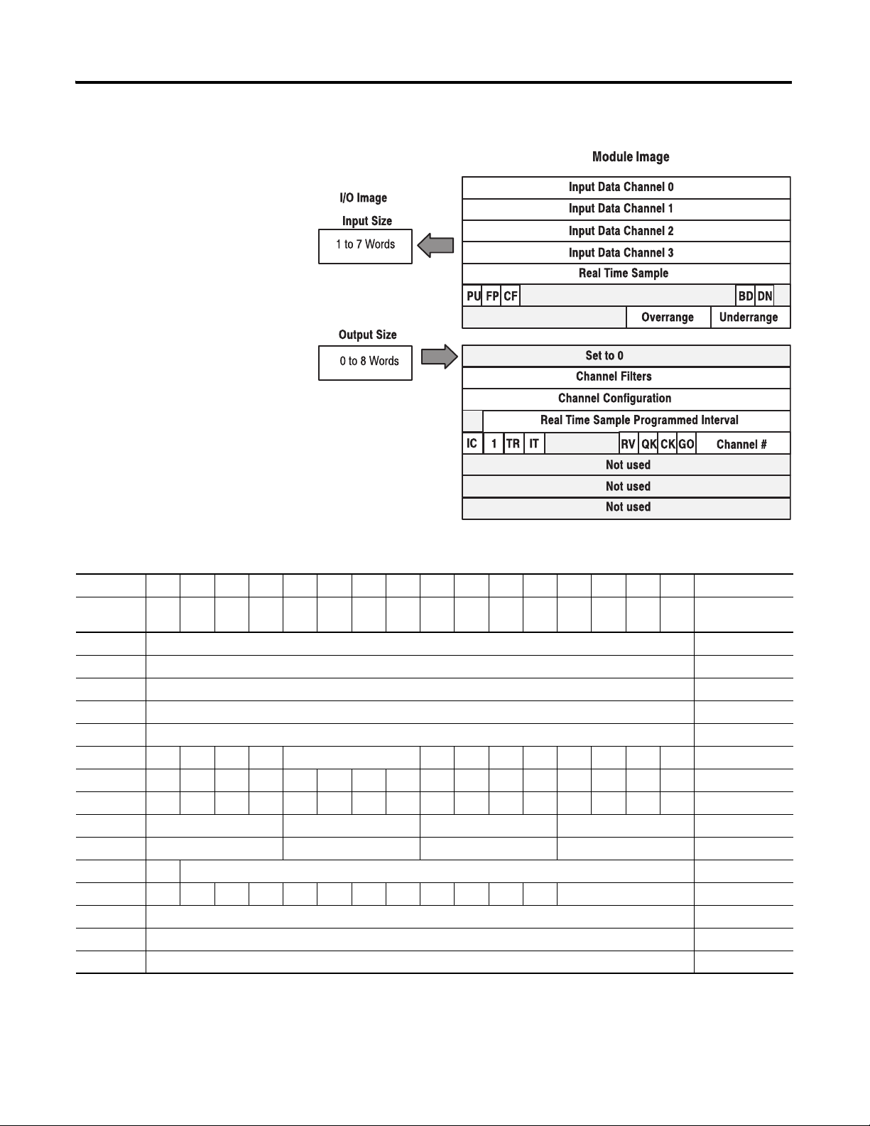
Communicate With Your Module 43
1147
1794-IF4I – 4-Input Isolated Analog Module Image Table Mapping
1794-IF4I Isolated Analog Input Module Read Words
Dec. Bit 15141312111009080706050403020100Size
Octal Bit 17 16 15 14 13 12 11 10 07 06 05 04 03 02 01 00 Read/Write
Analog Value Channel 0 Read Word 0
Analog Value Channel 0 Read Word 1
Analog Value Channel 0 Read Word 2
Analog Value Channel 0 Read Word 3
Real Time Sample Read Word 4
PUFPCF0Reserved 00000BDDN0Read Word 5
00000000V3V2V1V0U3U2U1U0Read Word 6
0000000000000000Write Word 0
Chnl 3 Filter Chnl 2 Filter Chnl 1 Filter Chnl 0 Filter Write Word 1
Chnl 3 Configuration Chnl 2 Configuration Chnl 1 Configuration Chnl 0 Configuration Write Word 2
0 Real Time Sample Programmed Interval Write Word 3
IC 1 TR IT 0 0 0 0 RV QK CK GO Channel Number Write Word 4
Not used Write Word 5
Not used Write Word 6
Word 7 Not used Write Word 7
Words
Publication 1794-UM064B-EN-P - May 2014
Page 56

44 Communicate With Your Module
1794-IF4I Isolated Analog Input Module Read Words
Dec. Bit 15141312111009080706050403020100Size
Octal Bit 17 16 15 14 13 12 11 10 07 06 05 04 03 02 01 00 Read/Write
Where: PU = Power up unconfigured state
FP = Field power off
CF = Configuration mode
BD = Calibration bad
DN = Calibration done
U = Underrange for specified channel
V = Overrange for specified channel
IC = Initiate configuration bit
TR = Transparent bit
IT = Interrupt toggle bit
RV = Revert to defaults bit
QK = Quick calibration
CK = Calibration clock
GO = Gain offset select
Words
Setting the Input Filter
Bits Channel
03 02 01 00 Input 0
07 06 05 04 Input 1
11 10 09 08 Input 2
15 14 13 12 Input 3
A/D Conversion Rate Low Pass Filter
00001200 Hz No low pass
00011200 Hz 100 ms low pass
00101200 Hz 500 ms low pass
00111200 Hz 1000 ms low pass
0100600 Hz No low pass
0101600 Hz 100 ms low pass
0110600 Hz 500 ms low pass
0111600 Hz 1000 ms low pass
1000300 Hz No low pass
1001300 Hz 100 ms low pass
1010300 Hz 500 ms low pass
1011300 Hz 1000 ms low pass
1100150 Hz No low pass
1101150 Hz 100 ms low pass
1110150 Hz 500 ms low pass
1111150 Hz 1000 ms low pass
Publication 1794-UM064B-EN-P - May 2014
Page 57

Communicate With Your Module 45
Configuring Your Input Channel
Input Channel Configuration
03 02 01 00 Set these bits for Channel 0.
07 06 05 04 Set these bits for Channel 1.
11 10 09 08 Set these bits for Channel 2.
15 14 13 12 Set these bits for Channel 3.
Bit Settings Input
Values
Data Format % Underrange/
% Overrange
Input Range
Hexadec. Dec.
0000Channel not configured
00014...20 mA signed 2’s complement 4% Under; 4% Over<0000...7878> <0000...30840> 7.5 ms 5.0 ms
0010± 10V signed 2’s complement 2% Under; 2% Over<831F...7CE1><-31969...31969>2.5 ms 2.5 ms
0011± 5V signed 2’s complement 4% Under; 4% Over<8618...79E8> <-31208...31208> 2.5 ms 2.5 ms
01000...20 mA signed 2’s complement % 0% Under; 4% Over<0...2710> <0...10000> 7.5 ms 5.0 ms
01100...10V signed 2’s complement % 0% Under; 2% Over<0...2710> <0...10000> 5.0 ms 5.0 ms
0111± 10V singed 2’s complement % 2% Under; 2% Over<-D8F0...2710><-10000...10000>5.0 ms 5.0 ms
10000...20 mA binary 0% Under; 4% Over<0000...F3CF> <0000...62415> 2.5 ms 2.5 ms
10014...20 mA
(1)
binary 4% Under; 4% Over <0000...F0F1> <0000...61681> 7.5 ms 5.0 ms
10100...10V binary 0% Under; 2% Over<0000...F9C2> <0000...63938> 2.5 ms 2.5 ms
10110...5V binary 0% Under; 4% Over<0000...F3CF> <0000...62415> 2.5 ms 2.5 ms
1100± 20 mA offset binary, 8000H = O mA4% Under; 4% Over<0618...F9E8> <1560...63976> 2.5 ms 2.5 ms
11014...20 mA offset binary, 8000H = 4 mA4% Under; 4% Over<8000...F878> <32768...63608> 7.5 ms 5.0 ms
1110± 10V offset binary, 8000H = OV 2% Under; 2% Over<031F...FCE1><799...64737> 2.5 ms 2.5 ms
1111± 5V offset binary, 8000H = OV 4% Under; 4% Over<0618...F9E8> <1560...63976> 2.5 ms 2.5 ms
(1)
Underrange for 4...20 mA occurs in the blind area below 0 (3.2 mA).
(2)
<and> indicates the overrun beyond actual range (about 5%).
(2)
Module Update Rate
(RTSI = 0) (RTSI = 0),
IT = 1
1794-IF4I Isolated Analog Input Module Word/Bit Descriptions
Word Decimal Bit
(Octal Bit)
Read Word 0 Bit 00…15
(00…17)
Read Word 1 Bit 00…15
(00…17)
Read Word 2 Bit 00…15
(00…17)
Read Word 3 Bit 00…15
(00…17)
Read Word 4 Bit 00…15
(00…17)
Definition
Channel 0 Analog Data – Real time input data per your configuration.
Channel 1 Analog Data – Real time input data per your configuration.
Channel 2 Analog Data – Real time input data per your configuration.
Channel 3 Analog Data – Real time input data per your configuration.
Real Time Sample – the elapsed time in increments programmed by the real time
sample interval.
Publication 1794-UM064B-EN-P - May 2014
Page 58

46 Communicate With Your Module
1794-IF4I Isolated Analog Input Module Word/Bit Descriptions
Word Decimal Bit
(Octal Bit)
Read Word 5 Bit 00 Reserved.
Bit 01 Calibration Done bit (DN) – This bit is set to 1 after a calibration cycle is
Bit 02 Calibration Bad bit (BD) – This bit is set to 1 if the channel calibration coefficients
Bits 03…07 Set to 0.
Bits 08…11
(10…12)
Bit 12 (14) Set to 0.
Bit 13 (15) Configuration Mode bit (CF) – This bit is set (1) when the calibration mode is
Bit 14 (16) Field Power Off bit (FP) – This bit is set (1) when the 24V field power fails. When
Bit 15 (17) Power Up (unconfigured state) bit (PU) – This bit is set (1) when the configuration
Read Word 6 Bits 00…03 Underrange bits (U) -These bits are set (1) when the input channel is below a preset
Bits 04…07 Overrange bits (V) – These bits are set (1) when the input channel is above a preset
Bits 08…15
(10…17)
Write Word 0 Bits 00…14
(00…16)
Write Word 1 Channels 0...3 Filter Selections (refer to Setting the Input Filter)
Bits 00…03 Channel 0 Filter Setting.
Bits 04…07 Channel 1 Filter Setting.
Bits 08…11
(10…13)
Bits 12…15
(14…17)
Write Word 2 Channel Configuration (See Configuring Your Input Channel
Bits 00…03 Channel 0 Configuration.
Bits 04…07 Channel 1 Configuration.
Bits 08…11
(10…13)
Bits 12…15
(14…17)
Write Word 3 Bits 00…14
(00…16)
Bit 15 (17) Not used. Set to 0.
Definition
completed.
cannot be saved or be read properly.
Reserved.
selected (bit 15, word 5 in the block transfer write set to 1). When this bit is set (1),
the module status indicator flashes.
this bit is set (1), the module status indicator flashes.
word is all zeroes (0) due to a reset (adapter power cycle or module insertion) or a
cleared configuration word (all 0). When this bit is set (1), the module status indicator
flashes.
limit as defined by the configuration selected. U0 (bit 00) corresponds to input channel
0 and U1 (bit 01) corresponds to input channel 1, and so on. See Configuring Your
Input Channel on page 45.
limit as defined by the configuration selected. Bit 04 corresponds to input channel 0
and bit 05 corresponds to input channel 1, and so on. See Configuring Your Input
Channel on page 45.
Not used. Set to 0.
Not used. Set to 0.
Channel 2 Filter Setting.
Channel 3 Filter Setting.
on page 45.)
Channel 2 Configuration.
Channel 3 Configuration.
Real Time Sample Interval – Programs the interval of the real time sample. Can be
varied from 0...30 s (3000 decimal). Resolution is in ms with granularity in 5 ms steps.
Publication 1794-UM064B-EN-P - May 2014
Page 59

1794-IF4I Isolated Analog Input Module Word/Bit Descriptions
Communicate With Your Module 47
Word Decimal Bit
Write Word 4 Bit 00…03 Channel Calibration Selection bit. – When this bit is set (1), the channel can be
Write Words
5…7
(Octal Bit)
Bit 04 Gain/Offset Calibration bit (GO) – When this bit is cleared, a 0...1...0 transition of
Bit 05 Calibration Clock bit (CK) – When this bit is set to 1 (calibration mode), the
Bit 06 Quick Calibration bit (QK) – Normally reset (0). When this bit is set (1) during a
Bit 07 Revert to Defaults bits (RV) – Normally reset (0). When set (1) during a calibration
Bit 08…11
(10…14)
Bit 12 (14) Interrupt Toggle bit (IT) – This bit, when set (1), permits interleaving of module
Bit 13 (15) Transparent bit (TR) – This bit, when set to 1, permits configuration to be changed
Bit 14 (16) Set to 1.
Bit 15 (17) Initiate Configuration bit (IC) – When set (1), instructs the module to enter
Bits 00…15
(00…17)
Definition
calibrated using the calibration clock bit (CK). Bit 00 corresponds to input channel 0,
bit 01 corresponds to channel 1, bit 02 corresponds to input channel 2, bit 03
corresponds to input channel 3.
the CK bit performs on offset calibration. When this bit is 1, the module is directed to
do a gain calibration.
calibration coefficient for the selected channels is accepted. When this bit is reset (0),
the accepted calibration coefficients for the selected channels are stored, applied,
and the calibration mode exited. Monitor status bits DN and BD for
successful calibration.
calibration sequence, the calibration coefficient is stored to all related configurations
for the selected channels.
NOTE: This method of calibration quickly calibrates the selected channels, however
you will not be within the rated accuracy of the module.
procedure, default values for selected channels are used for the calibration
coefficient.
NOTE: You will not be within the rated accuracy of the module.
Not used. Set to 0.
interrupts ensuing exchange of critical data when channels are configured for their
fastest update times. RTSI and "no low pass filter" must be 0 in order for the module
to recognize this feature. This groups data update rates for all channels to the slowest
configuration setting of any of the channels. In addition, channel update rates for all
channels with a 7.5 ms update rate are reduced to 5.0 ms. When reset (0), real time
sampling and filter features are enabled.
without using the IC bit.
configuration mode. Present configuration data prior to or coincident with IC being
set. Once IC returns to 0, the configuration is applied and any subsequent
configuration information is ignored until IC is toggled.
Not used.
Publication 1794-UM064B-EN-P - May 2014
Page 60

48 Communicate With Your Module
1148
1794-OF4I – 4-Output Isolated Analog Module Image Table Mapping
1794-OF4I Isolated Analog Output Module Read Words
Word/Dec. Bit 15141312111009080706050403020100
Word/Octal Bit 17161514131211100706050403020100
Read Word 0 Read Back Channel 0
Read Word 1 Read Back Channel 1
Read Word 2 Read Back Channel 2
Read Word 3 Read Back Channel 3
Read Word 4 PUFPCF0Reserved 00000BDDN0
Read Word 5 0000P3P2P1P00000W3W2W1W0
Write Word 0 ENS1S00000000000000
Write Word 1 Output Data – Channel 0
Write Word 2 Output Data – Channel 1
Write Word 3 Output Data – Channel 2
Write Word 4 Output Data – Channel 3
Write Word 5 Output Ch 3
Configuration
Output Ch 2
Configuration
Output Ch 1
Configuration
Output Ch 0
Configuration
Publication 1794-UM064B-EN-P - May 2014
Page 61

Communicate With Your Module 49
1794-OF4I Isolated Analog Output Module Read Words
Word/Dec. Bit 15141312111009080706050403020100
Word/Octal Bit 17161514131211100706050403020100
Write Word 6 IC 1 TR IT Q3 Q2 Q1 Q0 RV QK CK GO Channel Number
Write Words
7 and 8
Where: PU = Power up unconfigured state
Not used
FP = Field power off
CF = In configuration mode
BD = Calibration bad
OR = Reference calibration signal is out of range
P0...P3 = Output holding in response to Q0...Q3
W0...W3 =Wire off current loop status for channels 0...3 respectively — Not used on voltage outputs.
EN = Enable outputs; 0 = output follows S1/S0, 1 = output enabled
IC = Initiate configuration bit
TR = Transparent bit
IT = Interleave Interrupts
Q0...Q3 = Request for outputs to hold
RV = Revert to defaults bit
QK = Quick calibration
CK = Calibration clock
GO = Gain offset calibration
1794-OF4I – Isolated Output Module Output Configuration
Configuration Bits
MSD LSD
Nominal
Range
Data Type Output Values
Hexadecimal Decimal
0 0 0 1 4...20 mA 2’s complement <0000..7878> <0000...30840> 5.0 ms
0 0 1 0 ±10V 2’s complement <831F...79E8> <-31208...31208> 2.5 ms
0 0 1 1 ±5V 2’s complement <8618...79E8> <-31208...31208> 2.5 ms
0 1 0 0 0...20 mA 2’s complement % <0...2710> <0...10000> 5.0 ms
0 1 0 1 4...20V 2’s complement % <0...2710> <0...10000> 5.0 ms
0 1 1 0 0...10V 2’s complement % <0...2710> <0...10000> 5.0 ms
0 1 1 1 ± 10V 2’s complement <-D8F0...2710> <-10000...10000> 5.0 ms
1 0 0 0 0...20 mA binary <0000...F3CF> <0000...62415> 2.5 ms
1 0 0 1 4...20 mA binary <0000...F0F1> <0000...61681> 5.0 ms
1 0 1 0 0...10V binary <0000...F3CF> <0000...62415> 2.5 ms
1 0 1 1 0...5V binary <0000...F3CF> <0000...62415> 2.5 ms
1 1 0 0 ±2 0 mA offset binary <0000...F9E8> <0000...63976> 2.5 ms
1 1 0 1 4...20 mA offset binary <8000...F878> <32768...63608> 5.0 ms
1 1 1 0 ± 10V offset binary <0618...F9E8> <1560...63976> 2.5 ms
1 1 1 1 ± 5V offset binary <0618...F9E8> <1560...63976> 2.5 ms
(1)
< and > indicate the overrun beyond actual range (about 5%).
(1)
Update
Rate
Publication 1794-UM064B-EN-P - May 2014
Page 62

50 Communicate With Your Module
1794-IF4I Isolated Analog Input Module Word/Bit Descriptions
Read Word Decimal Bit
(Octal Bit)
Read Word 0 Bit 00…15
(00…17)
Read Word 1 Bit 00…15
(00…17)
Read Word 2 Bit 00…15
(00…17)
Read Word 3 Bit 00…15
(00…17)
Read Word 4 Bit 00 Reserved.
Bit 01 Calibration Done bit (DN) – This bit is set to 1 after a calibration cycle
Bit 02 Calibration Bad bit (BD) – This bit is set to 1 if the channel calibration coefficients
Bits 03…07 Set to 0.
Bits 08…11
(10…12)
Bit 12 (14) Set to 0.
Bit 13 (15) Configuration Mode bit (CF) – This bit is set (1) when the calibration mode is
Bit 14 (16) Field Power Off bit (FP) – This bit is set (1) when the 24V field power fails. When
Bit 15 (17) Power Up (unconfigured state) bit (PU) – This bit is set (1) when the configuration
Read Word 5 Bits 00…03 Wire-off Status bits (W) – These bits, when set (1), indicate the corresponding
Bits 04…07 Set to 0.
Bits 10…11
(12…13)
Bits 12…15
(13…17)
Definition
Read Back Channel 0 – During normal operation, it is a copy of the output of
channel 0. During an EN transition, it is the condition of the output as determined by
S1 and S0. Read back is an image of what the user has sent as output to the module;
no checks are performed on the data.
Read Back Channel 1 – During normal operation, it is a copy of the output of
channel 1. During an EN transition, it is the condition of the output as determined by
S1 and S0. Read back is an image of what the user has sent as output to the module;
no checks are performed on the data.
Read Back Channel 2 – During normal operation, it is a copy of the output of
channel 2. During an EN transition, it is the condition of the output as determined by
S1 and S0. Read back is an image of what the user has sent as output to the module;
no checks are performed on the data.
Read Back Channel 3 – During normal operation, it is a copy of the output of
channel 3. During an EN transition, it is the condition of the output as determined by
S1 and S0. Read back is an image of what the user has sent as output to the module;
no checks are performed on the data.
is completed.
cannot be saved or be read properly.
Reserved.
selected (bit 15, word 5 in the block transfer write set to 1). When this bit is set (1),
the module status indicator flashes.
this bit is set (1), the module status indicator flashes.
word is all zeroes (0) due to a reset (adapter power cycle or module insertion) or a
cleared configuration word (all 0). When this bit is set (1), the module status
indicator flashes.
current output channel is open. W0 corresponds to channel 0, W1 corresponds to
channel 2, and so on.
Hold Output bits (P) – These bits are set (1) in response to Q0 or Q1 and a transition
of the EN bit. When P0 or P1 is set (1), they indicate that the output is holding at the
level in the readback data for the respective channel. These bits return to 0 when the
output data matches the readback output data.
Set to 0.
Publication 1794-UM064B-EN-P - May 2014
Page 63

1794-IF4I Isolated Analog Input Module Word/Bit Descriptions
Communicate With Your Module 51
Write Word Decimal Bit
(Octal Bit)
Write Word 0 Bit 00…12
(00…14)
Bit 13…14
(15…16)
Bit 15 (17) Output Enable bit (EN) – When set (1), the outputs are enabled. This bit must be set in
Write Word 1 Bit 00…15
(00…17)
Write Word 2 Bit 00…15
(00…17)
Write Word 3 Bit 00…15
(00…17)
Write Word 4 Bit 00…15
(00…17)
Write Word 5 Channel Configuration (see 1794-OF4I Isolated Analog Output Module Read Words
Bits 00…03 Channel 0 Configuration
Bit 04…07 Channel 1 Configuration
Bit 08…11
(10…13)
Bit 12…15
(14…17)
Definition
Not used.
Safe State Configure (S1/S0) – When EN is 0, these bits designate the source of the
safe state data.
Bit 13 = 0, bit 14 = 1 – reset outputs to 0V/0mA (used with 1794-ASB/C)
Bit 13 = 1, bit 14 = 1 – hold output at its current level (used with 1794-ASB/C)
Bit 13 = 0, bit 14 = 0 – Safe state data is in output data words
order for the real time data to appear at the outputs. If this bit is not set (0), the outputs
will be determined by S1/S0.
Channel 0 output data – The output data is real time data formatted to the selected
configuration. This data is also safe state data when directed by S1 and S0.
Channel 1 output data – The output data is real time data formatted to the selected
configuration. This data is also safe state data when directed by S1 and S0.
Channel 2 output data – The output data is real time data formatted to the selected
configuration. This data is also safe state data when directed by S1 and S0.
Channel 3 output data – The output data is real time data formatted to the selected
configuration. This data is also safe state data when directed by S1 and S0.
Channel 2 Configuration
Channel 3 Configuration
on page 48)
Publication 1794-UM064B-EN-P - May 2014
Page 64

52 Communicate With Your Module
1794-IF4I Isolated Analog Input Module Word/Bit Descriptions
Write Word Decimal Bit
Write Word 6 Bits 00…03 Calibrate bit – When this bit is set (1), the channel can be calibrated using the
Write Words
7 and 8
(Octal Bit)
Bit 04 Gain/Offset Calibration bit (GO) – When this bit is cleared, a 0 to 1 to 0 transition of
Bit 05 Calibration Clock bit (CK) – When this bit is set to 1 (calibration mode), the
Bit 06 Quick Calibration bit (QK) – Normally reset (0). When this bit is set (1) during a
Bit 07 Revert to Defaults bit (RV) – Normally reset (0). When set (1) during a calibration
Bits 08…11
(10…13)
Bit 12 (14) Interleave Interrupt (IT) – This bit, when set (1), permits interleaving of module
Bit 13 (15) Transparent bit (TR) – This bit, when set (1), permits configuration to be changed
Biut 14 (16) Set to 1.
Bit 15 (17) Initiate Configuration bit (IC) – When set (1), instructs this the module to enter
Bits 00…15
(00…17)
Definition
calibration clock bit (CK). Bit 00 corresponds to output channel 0, bit 01 corresponds to
output channel 1, bit 02 corresponds to output channel 3, bit 03 corresponds to output
channel 4.
the CK bit performs on offset calibration. When this bit is set (1), the module is directed
to do a gain calibration.
calibration coefficient for the selected channels is accepted. When this bit is reset (0),
the accepted calibration coefficients for the selected channels are stored, applied, and
the calibration mode exited. Monitor status bits DN and BD for successful calibration.
calibration sequence, the calibration coefficient is stored to all related configurations
for the selected channels.
NOTE: Although this method of calibration quickly calibrates the selected channels,
they will not be within the rated accuracy of the module.
procedure, default values for selected channels are used for the calibration coefficient.
NOTE: They will not be within the rated accuracy of the module.
Request for Hold Outputs (Q) – Channel request bits that instruct and output to hold
its output level when EN transitions from 1 to 0 to 1. When EN is 0, outputs go to a save
state dictated by S1/S0. When EN returns to 1, the outputs will hold their level until the
output data equals the output level. P0...P3 indicates channels holding. Output read
back data shows what level is being held. Q0 = bit 08 (10) = channel 0; Q1 = bit 08 (10) =
channel 1, and so on.
interrupts ensuring exchange of critical data when channels are configured for their
fastest update times. RTSI and "no low pass filter" must be 0 in order for the module to
recognize this feature. This groups data update rates for all channels to the slowest
configuration setting of any of the channels. In addition, channel update rates for all
channels with a 7.5 ms update rate are reduced to 5.0 ms. When reset (0), real time
sampling and filter features are enabled.
without using the IC bit.
configuration mode. Present configuration data prior to or coincident with IC being set.
Once IC returns to 0, the configuration is applied and any subsequent configuration
information is ignored until IC is toggled.
Not used.
Publication 1794-UM064B-EN-P - May 2014
Page 65

Communicate With Your Module 53
1149
1794-IF2XOF2I Series B – Isolated Analog Combo Module Image Table Mapping
1794-IF2XOF2I – Isolated Analog Combo Module Read Words
Word/Dec. Bit 15141312111009080706050403020100
Word/Octal Bit 17161514131211100706050403020100
Read Word 0 Input Data Channel 0
Read Word 1 Input Data Channel 1
Read Word 2 Read Back Channel 0
Read Word 3 Read Back Channel 1
Read Word 4 0 Real Time Sample
Read Word 5 PUFPCF0Reserved 00000BDDN0
Read Word 6 0000P1P00000V1V0W1W0U1U0
Write Word 0 ENS1S00000000000000
Write Word 1 Output Data – Channel 0
Write Word 2 Output Data – Channel 1
Write Word 3 00000000Input Channel 1 Filter Input Channel 0 Filter
Write Word 4 Output Channel 1
Configuration
Write Word 5 0 Real Time Sample Programmed Interval
Output Channel 0
Configuration
Input Channel 1
Configuration
Input Channel 0
Configuration
Publication 1794-UM064B-EN-P - May 2014
Page 66

54 Communicate With Your Module
1794-IF2XOF2I – Isolated Analog Combo Module Read Words
Word/Dec. Bit 15141312111009080706050403020100
Word/Octal Bit 17161514131211100706050403020100
Write Word 6 IC 1 TR IT Q1 Q0 0 0 RV QK CK GO Channel Number
Write Word 7 Not used
Where: PU = Power up unconfigured state
FP = Field power off
CF = Configuration mode
BD = Calibration bad
DN = Calibration accepted
P0 and P1 = Output holding in response to Q0...Q1
W0 and W3 =Wire off current loop status for channels 0 and 1 respectively. (Not used on voltage outputs).
U0 and U1 = Underrange for input channels 0 and 1 respectively
V0 and V1 = Overrange for input channels 0 and 1 respectively
EN = Enable outputs; 0 = output follows S1/S0, 1 = output enabled
IC = Initiate configuration bit
TR = Transparent bit
IT = Interrupt toggle bit
Q0 and Q1 = Hold
RV = Revert to defaults bit
QK = Quick calibration
CK = Calibration clock
GO = Gain offset select
Configure Your Input Channels
Input Channel Configuration
03020100Set these bits for Channel 0
07060504Set these bits for Channel 1
Bit Settings Input
Values
Data Format % Underrange/
% Overrange
Input Range
Hexadec. Dec.
0000Channel not configured
00014...20 mA signed 2’s complement 4% Under; 4% Over <0000...7878> <0000...30840> 7.5 ms 5.0 ms
0010± 10V signed 2’s complement 2% Under; 2% Over <831F...7CE1> <-31969...31969>2.5 ms 2.5 ms
0011± 5V signed 2’s complement 4% Under; 4% Over <8618...79E8> <-31208...31208> 2.5 ms 2.5 ms
01000...20 mA signed 2’s complement % 0% Under; 4% Over <0...2710> <0...10000> 7.5 ms 5.0 ms
01014...20 mA signed 2’s complement % 4% Under, 4% Over <0...2710> <0...10000> 7.5 ms 5.0 ms
01100...10V signed 2’s complement % 0% Under; 2% Over <0...2710> <0...10000> 5.0 ms 5.0 ms
0111± 10V singed 2’s complement % 2% Under; 2% Over <-D8F0...2710><-10000...10000>5.0 ms 5.0 ms
10000...20 mA binary 0% Under; 4% Over <0000...F3CF> <0000...62415> 2.5 ms 2.5 ms
10014...20 mA
(1)
binary 4% Under; 4% Over <0000...F0F1> <0000...61681> 7.5 ms 5.0 ms
10100...10V binary 0% Under; 2% Over <0000...F9C2> <0000...63938> 2.5 ms 2.5 ms
10110...5V binary 0% Under; 4% Over <0000...F3CF> <0000...62415> 2.5 ms 2.5 ms
1100± 20 mA offset binary, 8000H = 0 mA4% Under; 4% Over <0618...F9E8> <1560...63976> 2.5 ms 2.5 ms
11014...20 mA offset binary, 8000H = 4 mA 4% Under; 4% Over <8000...F878> <32768...63608> 7.5 ms 5.0 ms
1110± 10V offset binary, 8000H = 0V 2% Under, 2% Over <031F...FCE1> <799...64737> 2.5 ms 2.5 ms
± 5V offset binary, 8000H = 0V 4% Under, 4% Over <0618...F9E8> <1560...63976> 2.5 ms 2.5 ms
(1)
Underrange for 4...20 mA occurs in the blind area below 0 (3.2 mA).
(2)
Module Update Rate
(RTSI = 0) (RTSI = 0), IT = 1
Publication 1794-UM064B-EN-P - May 2014
Page 67

Communicate With Your Module 55
Setting the Input Filters
Bits Channel
03 02 01 00 Input Channel 0
07 06 05 04 Input Channel 1
A/D Conversion Rate Low Pass Filter
00001200 Hz No low pass
00011200 Hz 100 ms low pass
00101200 Hz 500 ms low pass
00111200 Hz 1000 ms low pass
0100600 Hz No low pass
0101600 Hz 100 ms low pass
0110600 Hz 500 ms low pass
0111600 Hz 1000 ms low pass
1000300 Hz No low pass
1010300 Hz 100 ms low pass
1011300 Hz 500 ms low pass
1100300 Hz 1000 ms low pass
1101150 Hz No low pass
1110150 Hz 100 ms low pass
1111150 Hz 500 ms low pass
150 Hz 1000 ms low pass
(2)
<and> indicates the overrun beyond actual range (about 5%).
Configure Your Output Channels
Configuration Bits
MSD LSD
00014...20 mA 2’s complement <0000...7878> <0000...30840> 5.0 ms
0010± 10V 2’s complement <8618...79E8> <-31208...31208> 2.5 ms
0011± 5V 2’s complement <8618...79E8> <-31208...31208> 2.5 ms
01000...20 mA 2’s complement % <0...10000> <0...10000> 5.0 ms
01014...20 mA 2’s complement % <0...10000> <0...10000> 5.0 ms
01100...10V 2’s complement % <0...10000> <0...10000> 5.0 ms
0111± 10V 2’s complement <-10000...10000> <-10000...10000> 5.0 ms
10000...20 mA binary <0000...F3CF> <0000...62415> 2.5 ms
10014...20 mA binary <0000...F0F1> <0000...61681> 5.0 ms
10100...10V binary <0000...F3CF> <0000...62415> 2.5 ms
10110...5V binary <0000...F3CF> <0000...62415> 2.5 ms
11004...20 mA offset binary <8000...F9E8> <32768...63976> 2.5 ms
Nominal
Range
Data Type Output Values
Hexadecimal Decimal
Update
Rate
Publication 1794-UM064B-EN-P - May 2014
Page 68

56 Communicate With Your Module
Configure Your Output Channels
Configuration Bits
MSD LSD
1 1 0 1 ± 20 mA offset binary <8000...F878> <32768...63608> 5.0 ms
1 1 1 0 ± 10V offset binary <0618...F9E8> <1560...63976> 2.5 ms
1 1 1 1 ± 5V offset binary <0618...F9E8> <1560...63976> 2.5 ms
Nominal
Range
Data Type Output Values
Hexadecimal Decimal
Update
Rate
1794-IF2XOF2I Analog Combo Module Word/Bit Descriptions
Word Decimal Bit
(Octal Bit)
Read Word 0 Bit 00…15
(00…17)
Read Word 1 Bit 00…15
(00…17)
Read Word 2 Bits 00…15
(00…17)
Read Word 3 Bit 00…15
(00…17)
Read Word 4 Bit 00…15
(00…17)
Read Word 5 Bit 00 Reserved.
Bit 01 Calibration Done bit (DN) – This bit is set to 1 after a calibration cycle is completed.
Bit 02 Calibration Bad bit (BD) – This bit is set to 1 if the channel calibration coefficients cannot be
Bits 03…07 Set to 0.
Bits 08…11
(10…12)
Bit 12 (14) Set to 0.
Bit 13 (15) Configuration mode bit (CF) – This bit is set (1) when the calibration mode is selected (bit 15,
Bit 14 (16) Field Power Off bit (FP) – This bit is set (1) when the 24V field power fails. When this bit is
Bit 15 (17) Power Up (unconfigured state) bit (PU) – This bit is set (1) when the configuration word is
Definition
Input Channel 0 input data – 16-bit unipolar; 15-bit plus sign bipolar.
Input Channel 1 input data – 16-bit unipolar; 15-bit plus sign bipolar.
Read Back Output Channel 0 – During normal operation, it is a copy of the output of channel
0. During an EN transition, it is the condition of the output as determined by S1 and S0.
Read Back Output Channel 0 – During normal operation, it is a copy of the output of channel
0. During an EN transition, it is the condition of the output as determined by S1 and S0.
Real Time Sample – The fixed time period you set telling the module when to provide data to
the processor.
saved or be read properly.
Reserved.
word 5 in the block transfer write set to 1).
set (1), the module status indicator flashes.
all zeroes (0) due to a reset (adapter power cycle or module insertion) or a cleared configuration
word (all 0).
Publication 1794-UM064B-EN-P - May 2014
Page 69

1794-IF2XOF2I Analog Combo Module Word/Bit Descriptions
Communicate With Your Module 57
Word Decimal Bit
(Octal Bit)
Read Word 6 Bits 00…01 Underrange bits (U) – These bits are set (1) when the input channel is below a preset limit as
Bits 02…03 Wire-Off status bits (W) – These bits, when set (1), indicate the corresponding current output
Bits 04…05 Overrange bits – These bits are set (1) when the input channel is above a preset limit as
Bits 06…09
(06…11)
Bits 10…11
(12…13)
Bits 12…15
(14…17)
Write Word 0 Bits 00…12
(00…14)
Bit 13…14
(15…16)
Bit 15 (17) Output enable bit (EN) – When set (1), the outputs are enabled. This bit must be set in order
Write Word 1 Bits 00…15
(00…17)
Write Word 2 Bits 00…15
(00…17)
Write Word 3 Input Channels 0 and 1 Filter Selections. (See Setting the Input Filters on page 55).
Bits 00…01 Channel 0 Filter Setting
Bits 04…07 Channel 1 Filter Setting
Bits 8…15
(11…17)
Write Word 4 Channel Configuration
Bits 00…03 Input Channel 0 Configuration – See Configuring Your Input Channel
Bits 04…07 Input Channel 1 Configuration – See Configuring Your Input Channel on page 45
Bits 08…11
(10…13)
Bits 12…15
(14…17)
Write Word 5 Bits 00…14
(00…16)
Bit 15 (17) Set to 0.
Definition
defined by the configuration selected. U0 (bit 00) corresponds to input channel 0 and U1 (bit 01)
corresponds to input channel 1.
channel is open. W0 (bit 02) corresponds to channel 0, W1 (bit 03) corresponds to channel 1.
defined by the configuration selected. Bit 04 corresponds to input channel 0 and bit 05
corresponds to input channel 1.
Not used. Set to 0.
Hold output bits (P) – These bits are set (1) in response to Q0 or Q1 and a transition of the EN
bit. When P0 or P1 is set (1), they indicate that the output is holding at the level in the readback
data for the respective channel. These bits return to 0 when the output data matches the
readback output data.
Not used. Set to 0.
Not used.
Safe State Configure bits (S1/S0) – When EN is 0, these bits designate the source of the safe
state data.
Bit 13 = 0, bit 14 = 1 – reset outputs to 0V/0 mA
Bit 13 = 1, bit 14 = 1 – hold the output at its current level
for the real time data to appear at the outputs. If this bit is not set (0), the outputs will be
determined by S1/S0.
Output Channel 0 data. See Configure Your Output Channels
Output Channel 1 data. See Configure Your Output Channels
Set to 0.
Output Channel 0 Configuration – See Configuring Your Input Channel on page 45.
Output Channel 1 Configuration – See Configuring Your Input Channel
Real Time Sample Interval – Programs the interval of the real time sample. Can be varied
from 0...30 s (30000 decimal). Resolution is in ms with granularity in 5 ms steps.
on page 55.
on page 55.
on page 45
on page 45.
Publication 1794-UM064B-EN-P - May 2014
Page 70

58 Communicate With Your Module
1794-IF2XOF2I Analog Combo Module Word/Bit Descriptions
Word Decimal Bit
(Octal Bit)
Write Word 6 Bit 00…03 Channel Calibration Selection bit – When this bit is set (1), the channel can be claibrated
Bit 04 Gain/Offset Calibration bit (GO) – When this bit is set (1), a reset (0), set (1), reset (0) pattern
Bit 05 Calibration clock bit (CK) – When this bit is set to 1 (calibration mode), the calibration
Bit 06 Quick Calibration bit (QK) – Normally reset (0). When this bit is set (1) during a calibration
Bit 07 Revert to defaults bit (RV) – Normally reset (0). When set (1) during a calibration procedure,
Bits 08…09
(10…11)
Bits 10…11
(12…13)
Bit 12 (14) Interleave Interrupts (IT) – This bit, when set (1), permits interleaving of module interrupts
Bit 13 (15) Transparent bit (TR) – This bit, when set (1), permits configuration to be changed without
Bit 14 (16) Set to 1.
Bit 15 (17) Initiate Configuration bit (IC) – When set (1), instructs the module to enter configuration
Write Word 7 Bits 00…15
(00…17)
Definition
using the initiate calibration bit (IC). Bit 00 corresponds to input channel 0, bit 01 corresponds to
input channel 1, bit 02 corresponds to output channel 0, bit 03 corresponds to output channel 1.
of the calibration clock bit (CK) causes a gain calibration to occur. When this bit is set to 0, a
reset (0), set (1), reset (0) pattern of the calibration clock bit (CK) causes and offset calibration
to occur.
coefficient for the selected channels is accepted. When this bit is reset (0), the accepted
calibration coefficients are stored in the selected channels, applied, and the calibration mode
exited. Monitor status bits DN and BD for succesful calibration.
sequence, the calibration coefficient is stored to all related configurations for the selected
channels.
NOTE: This method of calibration quickly calibrates the selected channels, you will not be
within the rated accuracy of the module.
default values for selected channels are used for the calibration coefficient.
Not used. Set to 0.
Request for hold outputs (Q) – Channel request bits that instruct an output to hold its output
level when EN transitions from 0 to 1 to 0. When EN is 0, outputs go to a safe state dictated by
S1/S0. When EN returns to 1, the outputs will hold their level until the output data equals the
output level. P0...P3 indicates channels holding. Output read back data shows what level is
being held. Q0 = bit 08 (10) = channel 0; Q1 = bit 08 (10) = channel 1, and so on.
ensuring exchange of critical data when channels are configured for their fastest update times.
RTSI and "no low pass filter" must be 0 in order for the module to recognize this feature. This
groups data update rates for all channels to the slowest configuration setting of any of the
channels. In addition, channel update rates for all channels with a 7.5 ms update rate are
reduced to 5.0 ms. When reset (0), real time sampling and filter features are enabled.
using the IC bit.
mode. Present confirugation data prior to or coincident with IC being set. Once IC returns to 0,
additional configuration information is ignored.
Not used.
Publication 1794-UM064B-EN-P - May 2014
Page 71

Communicate With Your Module 59
1151
1794-ID2 – Incremental Encoder Module Image Table Mapping
1794-ID2 Pulse Counter Module Word/Bit Definitions for Block Transfer Read Words
Word Bit Definition
Read Word 0 Bit 00 Ch 0 Input A – (pulse transmitter 0) – This bit, when set, indicates a signal at A.
Bit 01 Ch 0 Input B – (pulse transmitter 0) – This bit, when set, indicates a signal at B.
Bit 02 Ch 0 Input Z – (pulse transmitter 0) – This bit, when set, indicates a signal at Z.
Bit 03 Ch 0 Input G – (pulse transmitter 0) – This bit, when set, indicates a signal at G.
Bit 04 Ch 1 Input A – (pulse transmitter 1) – This bit, when set, indicates a signal at A.
Bit 05 Ch 1 Input B – (pulse transmitter 1) – This bit, when set, indicates a signal at B.
Bit 06 Ch 1 Input Z – (pulse transmitter 1) – This bit, when set, indicates a signal at Z.
Bit 07 Ch 1 Input G – (pulse transmitter 1) – This bit, when set, indicates a signal at G.
Bit 08 (10) Calibrated 0 – This bit, when set (1), indicates that the counter 0 has been calibrated. This bit
Bit 09 (11) Calibrated 1 – This bit, when set (1), indicates that the counter 1 has been calibrated. This bit
Bit 10 (12) Ch 0 Counter Stored – This bit, when set (1), indicates a counter value is saved in store 0. This
is reset by CalReset.
is reset by CalReset.
bit is reset by StoreReset.
Publication 1794-UM064B-EN-P - May 2014
Page 72

60 Communicate With Your Module
1794-ID2 Pulse Counter Module Word/Bit Definitions for Block Transfer Read Words
Word Bit Definition
Read Word 0 Bit 11 (13) Ch 1 Counter Stored – This bit, when set (1), indicates a counter value is saved in store 1. This
Read Word 1 Bits 00…15
Read Word 2 Bits 00…15
Read Word 3 Bits 00…15
Read Word 4 Bits 00…15
Read Word 5 Bits 00…15
Read Word 7 Bits 00…15
Read Word 8 Bits 00…15
bit is reset by StoreReset.
Bit 12 (14) Ch 0 Preset Reached (PR0) – When this bit is set (1), in all configuration modes, the counter 0
value equals the preset 0 value, either in a positive or negative direction. This bit is reset by
PresetReset0 and can only be set again after at least 1 more pulse.
Bit 13 (15) Ch 1 Preset Reached (PR1) – When this bit is set (1), in all configuration modes, the counter 1
value equals the preset 0 value, either in a positive or negative direction. This bit is reset by
PresetReset1 and can only be set again after at least 1 more pulse.
Bit 14 (16) Ch 0 Counter Inc/Dec – 0 = last pulse decreased counter value, 1 = last pulse increased
counter value
Bit 15 (17) Ch 1 Counter In/Dec – 0 = last pulse decreased counter value, 1 = last pulse increased counter
value
Ch 0 Stored Counter – Saved counter value on channel 0.
(00…17)
Ch 1 Stored Counter – Saved counter value on channel 1.
(00…17)
Ch 0 Counter – Current value in counter 0.
(00…17)
Ch 1 Counter – Current value in counter 1.
(00…17)
Ch 0 Counter Readback – Counter word readback – last value written to write word 1.
(00…17)
Ch 1 Counter Readback – Counter word readback – last value written to write word 2.
(00…17)
Firmware Revision – identification of latest software version code.
(00…17)
1794-ID2 Pulse Counter Module Word/Bit Definitions for Block Transfer Read Words
Word Bit Definition
Write Word 0 0…15
(0…17)
Bits 00…02 02 01 00 Ch 0 Mode Selection bits
Bit 03 Ch 0 Counter Preset bit – A positive edge on this bit moves the value in Preset X to Counter X, independent of
Ch 0 Control – Control word for setting the function of Ch 0 Counter.
0 0 0 Counting on positive (rising) edge of input signal A (Up/dwn counting determined by B).
0 0 1 Quadrature encoder X1.
0 1 0 Quadrature encoder X2.
0 1 1 Quadrature encoder X4.
1 0 0 Counting up on positive edge of input signal A, and down on positive edge of input signal B.
1 0 1 No count function.
1 1 0 No count function.
1 1 1 No count function.
Preset Enable.
NOTE: To use Preset as Reset, use a count value of 0000 in the Preset value word.
Publication 1794-UM064B-EN-P - May 2014
Page 73

Communicate With Your Module 61
1794-ID2 Pulse Counter Module Word/Bit Definitions for Block Transfer Read Words
Word Bit Definition
Write Word 1 Bit 04 Ch 0 Z Preset Enable bit – When this bit is set (1), a positive edge on Z preloads Counter X = Preset X, independent of
Bit 05 Ch 0 Count Enable bit – When this is set (1), the incremental encoder is enabled.
Bits 06…08
(06…10)
Bits 09…10
(11…12)
Bits 11…12
(13…14)
Bit 13 (15) Ch 0 Rollover bit – When set (1), the counter counts up to the prset and then restarts at 0. If this bit is reset (0) (not
Bit 14 (16) Ch 0 Store Reset bit – A positive edge on this bit resets Stored X in Signals.
Bit 15 (17) Ch 0 Preset Reset bit – A positive edge on this bit resets Preset Detected in Signals.
Write Word 2 Ch 1 Control – Control word for setting the fuction of Ch 1 Counter.
Bits 00…02 Bit 02 01 00 Ch 1 Mode Selection bits
Cal Enable.
NOTE: If Z is configured to do Store and Preset (Reset), the Store will occur first.
Ch 0 Calibration Control bits – bits 06, 07 and 08.
06 Cal Enable bit – When set (1), the counter can be calibrated.
07 Cal Direction bit – When set (1), calibration is performed in a negative direction; when reset (0), calibration is
performed in a positive direction.
08 Ch 0 Cal Reset bit – Calibration is acknowledged and a new calibration is enabled on a positive edge on this bit.
10 09 Gate Control bits
0 0 No gate function on input G.
0 1 Counting only if G is high (active).
1 0 Counting only if G is low (inactive).
1 1 The counter can be calibrated when G is high (active).
12 11 Store Control bits
Save the counter value on positive edge of Z (if Stored X = 0).
Save the counter value on positive edge of G (if Stored X = 0).
Save the counter value on negative edge of G (if Stored X = 0).
Save the counter value on positive and negative edges of G (if Stored X = 0).
rollover), the rollover preset value = FFFF (hex = 65536 (decimal).
0 0 0 Counting on positive (rising) edge of input signal A (up/dwn counting determined by B).
0 0 1 Quadrature encoder X1.
0 1 0 Quadrature encoder X2.
0 1 1 Quadrature encoder X4.
1 0 0 Counting up on the positive edge of input signal A, and down on positive edge of input signal B.
1 0 1 No count function.
1 1 0 No count function.
1 1 1 No count function.
Publication 1794-UM064B-EN-P - May 2014
Page 74

62 Communicate With Your Module
1794-ID2 Pulse Counter Module Word/Bit Definitions for Block Transfer Read Words
Word Bit Definition
Write Word 2 Bit 03 Counter Preset bit – A positive edge on this bit moves the value in Preset X to Counter X, independent of Preset Enable.
Bit 04 Preset Enable bit – When set (1), a positive edge on Z preloads Counter X = Preset X, independent of Cal Enable.
Bit 05 Count Enable bit – When set (1), the incremental encoder is counting.
Bits 06…08
(06…10)
Bits 09…10
(11…12)
Bits 11…12
(13…14)
Bit 13 (15) Rollover bit – When set (1), the counter counts up to the preset and then restarts at 0. If this bit is reset (0) (not rollover),
Bit 14 (16) Ch 1 Preset Reset bit – A positive edge on this bit resets Stored X in Signals.
Bit 15 (17) Ch 1 Store Reset bit - A positive ege on this bit resets Preset Reached in Signals.
Write Word 3 Bits 00…15
Write Word 4 Bits 00…15
Write Word 5 Filter Selection
Write Words
6…7
(00…17)
(00…17)
Bit 00 Ch 0 Filter Enable – When set (1), and a counter 0 is in mode 000 (pulse counting), signal A0 is filtered by a digital low
Bit 01 Ch 1 Filter Enable – When set (1), and a counter 1 is in mode 000 (pulse counting), signal A1 is filtered by a digial low
Bit 02…07 Unused.
Bits 08…09
(10…11)09(11)08(10)
Bits 00…15
(00…17)
Calibration Control bits – bits 06, 07 and 08.
06 Enable bit – When set (1), the counter can be calibrated.
07 Direction bit – When set (1), calibration is performed in a negative direction; when reset (0), calibration is
performed in a positive direction.
08 Reset bit – Calibration is acknowledged and a new calibration is enabled on a positive edge on this bit.
10 09 Gate Control bits
0 0 No gate function on input G.
0 1 Counting only if G is high (active).
1 0 Counting only if G is low (inactive).
1 1 Calibration if G is high (active).
12 11 Latch Control bits
0 0 Save the counter value on the positive edge of Z (if Stored X = 0).
0 1 Save the counter value on the positive edge of G (if Stored X = 0).
1 0 Save the counter value on the negative edge of G (if Stored X = 0).
1 1 Save the counter value on the positive and negative edges of G (if Stored X = 0).
the rollover preset value = FFFF
hex = 65535 (decimal).
Ch 0 Preset – Value to load or compare with counter 0.
Ch 1 Preset – Value to load or compare with counter 1.
pass filter with selectable filter constant.
pass filter with selectable filter constant.
Filter bits – This constand is common to both counters.
0 0 73.5 kHz or minimum 0.007 ms pulsewidth.
0 1 37.8 kHz or minimum 0.013 ms pulsewidth.
1 0 12.8 kHz or minimum 0.04 ms pulsewidth.
1 1 1.2 kHz or minimum 0.4 ms pulsewidth.
Not used – set to 0.
Publication 1794-UM064B-EN-P - May 2014
Page 75
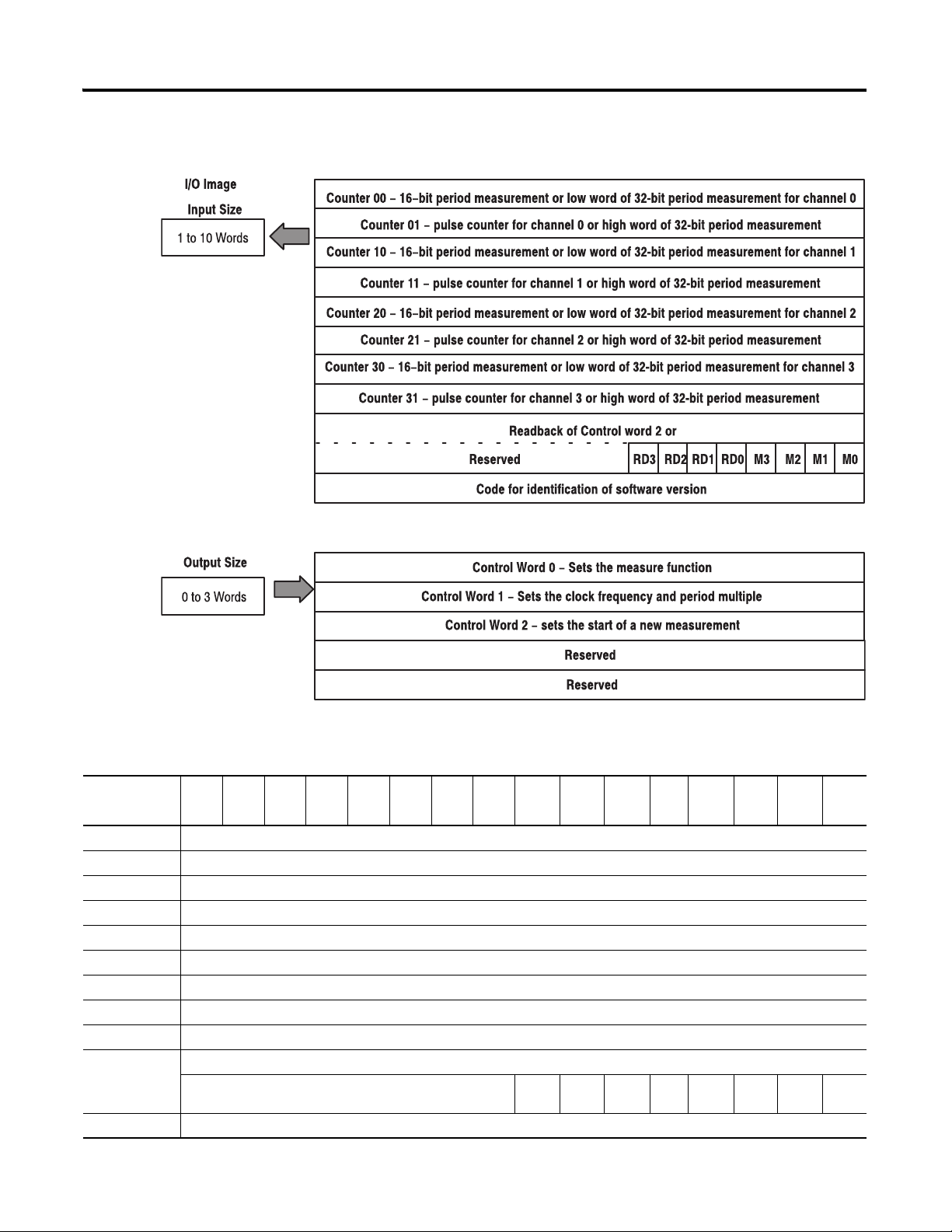
Communicate With Your Module 63
1151
1794-IP4 – Pulse Counter Module Image Table Mapping
1794-IP4 Pulse Counter Module Block Transfer Word Assignments
(Octal Bit ⇒ ) 17 16 15 14 13 12 11 10 07 06 05 04 03 02 01 00
Dec. Bit ⇒ 15 14 13 12 11 10 03 08 07 06 05 04 03 02 01 00
Word
⇓ Read
1 Ch 0 Data 0 – 16-bit period measurement or low word of 32-bit period measurement for channel 0.
2 Ch 0 Data 1 – pulse counter or high word of 32-bit period measurement for channel 0.
3 Ch 1 Data 0 – 16-bit period measurement or low word of 32-bit period measurement for channel 1.
4 Ch 1 Data 1 – pulse counter or high word of 32-bit period measurement for channel 1.
5 Ch 2 Data 0 – 16-bit period measurement or low word of 32-bit period measurement for channel 2.
6 Ch 2 Data 1 – pulse counter or high word of 32-bit period measurement for channel 2.
7 Ch 3 Data 0 – 16-bit period measurement or low word of 32-bit period measurement for channel 3.
8 Ch 3 Data 1 – pulse counter or high word of 32-bit period measurement for channel 3.
9Status.
Reserved. RD3 RD2 RD1 RD0 Ch 3
10 Revision read – software version code.
Publication 1794-UM064B-EN-P - May 2014
Ready
Ch 2
Ready
Ch 1
Ready
Ch 0
Ready
Page 76

64 Communicate With Your Module
1794-IP4 Pulse Counter Module Block Transfer Word Assignments
(Octal Bit ⇒ ) 17 16 15 14 13 12 11 10 07 06 05 04 03 02 01 00
Dec. Bit
Word
1 Control Word 0 – selects the measure function.
2 Control Word 1 – sets the clock frequency and period multiple.
3 Control Word 2 – sets the start of a new measurement.
4…5 Reserved.
Where: M = Positive edge measurement ready for the respective channel.
⇒ 15 14 13 12 11 10 03 08 07 06 05 04 03 02 01 00
⇓ Write
RD = Reset Done for respective channel.
1794-IP4 Pulse Counter Module Word/Bit Definitions
Word Bit Definition
Read Word 0 Bit 00…15
Read Word 1 Bit 00…15
Read Word 2 Bit 00…15
Read Word 3 Bit 00…15
Read Word 4 Bit 00…15
Read Word 5 Bit 00…15
Read Word 6 Bit 00…15
Read Word 7 Bit 00…15
Read Word 8 Bit Status
Read Word 9
(00…17)
(00…17)
(00…17)
(00…17)
(00…17)
(00…17)
(00…17)
(00…17)
Bit 00 Ch 0 Ready – measurement ready.
Bit 01 Ch 1 Ready – measurement ready.
Bit 02 Ch 2 Ready – measurement ready.
Bit 03 Ch 3 Ready – measurement ready.
Bit 04 Reset Done, Ch 0 – positive edge on this bit indicates counter 01 reset done.
Bit 05 Reset Done, Ch 1 – positive edge on this bit indicates counter 11 reset done.
Bit 06 Reset Done, Ch 2 – positive edge on this bit indicates counter 21 reset done.
Bit 07 Reset Done, Ch 3 – positive edge on this bit indicates counter 31 reset done.
Bit 08…15 Reserved for factory use.
Bits 00…15
(00…17)
Store Counter 00 – 16-bit period measurement or low word of 32-bit period measurement for channel 0.
Ch 0 Data 0 – pulse counter or high word of 32-bit period measurement for channel 0.
Ch 0 Data 1 – 16-bit period measurement or low word of 32-bit period measurement for channel 1.
Ch 1 Data 1 – pulse counter or high word of 32-bit period measurement for channel 1.
Ch 2 Data 0 – 16-bit period measurement or low word of 32-bit period measurement for channel 2.
Ch 2 Data 1 – pulse counter or high word of 32-bit period measurement for channel 2.
Ch 3 Data 0 – 16-bit period measurement or low word of 32-bit period measurement for channel 3.
Ch 3 Data 1 – pulse counter or high word of 32-bit period measurement for channel 3.
Software revision – Version code of software installed.
Publication 1794-UM064B-EN-P - May 2014
Page 77

1794-IP4 Pulse Counter Module Word/Bit Definitions
Word Bit Definition
Write Word 0 Bit Control Word 0 – Control word for setting the function of counter 0.
Bit 00 Pulse counting and period time measurement selection for Channel 0 –
Bit 01 Pulse counting and period time measurement selection for Channel 1 –
Bit 02 Pulse counting and period time measurement selection for Channel 2 –
Bit 03 Pulse counting and period time measurement selection for Channel 3 –
Bits 04…15
(04…17)
Write Word 1 Bit 00 Clock frequency for period time measurement - Channel 0 –
Bits 01…03 03 02 01 Number of periods for measurement - Channel 0.
Bit 04 Clock frequency for period time measurement - Channel 1 – see Bit 00 above.
Bits 05…07 Selection of Number of period for measurement - Channel 1 – see Bits 01…03 above.
Bits 08(10) Clock frequency for period time measurement - Channel 2 – see Bit 00 above.
Bits 09…11
(11…13)
Bit 12(14) Clock frequency for period time measurement - Channel 1 – see Bit 00 above.
Bits 13…15
(15…17)
0 = pulse counting and period measurement selected.
1 = period time measurement selected.
0 = pulse counting and period measurement selected.
1 = period time measurement selected.
0 = pulse counting and period measurement selected.
1 = period time measurement selected.
0 = pulse counting and period measurement selected.
1 = period time measurement selected.
Reserved.
0 = period time measurement with 10 MHz internal clock selected.
1 = period time measurement with 1 MHz internal clock selected.
0 0 0 1 period.
0 0 1 2 periods.
0 1 0 4 periods.
0 1 1 8 periods.
1 0 0 16 periods.
1 0 1 32 periods.
1 1 0 64 periods.
1 1 1 128 periods.
Selection of Number of period for measurement - Channel 2 – see Bits 01…03 above.
Selection of Number of periods for measurement - Channel 1 – see Bits 01…03 above.
Communicate With Your Module 65
Publication 1794-UM064B-EN-P - May 2014
Page 78
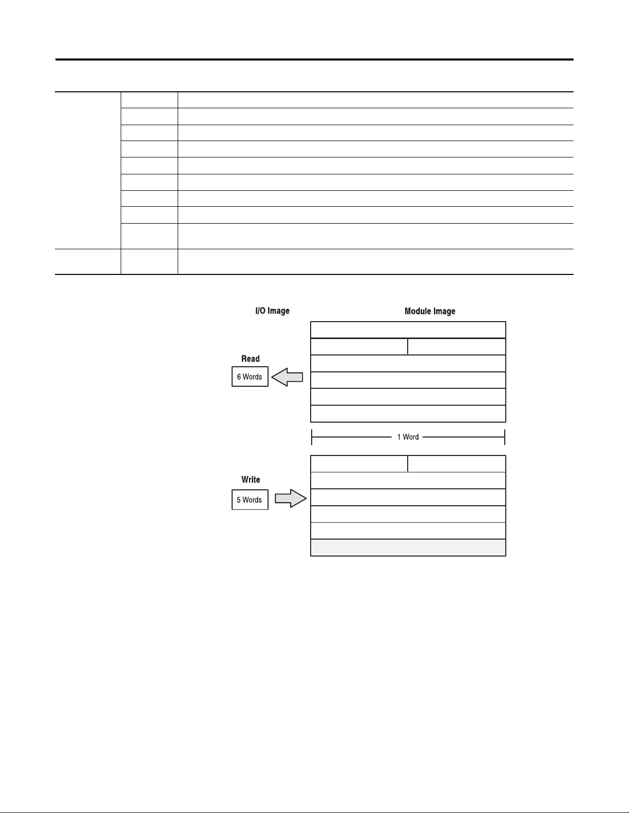
66 Communicate With Your Module
0
Logic Status Channel 1
Annalog Feedback Channel 1
Logic Command Channel 1
Annalog Reference Channel 1
Logic Command Channel 2
Annalog Reference Channel 2
Not Used
Logic Status Channel 2
Annalog Feedback Channel 2
Connection Status Channel 2 Connection Status Channel 1
Connection Enable Channel 2 Connection Enable Channel 1
1152
Write Word 2 Bit 00 Start new measurment bit - Channel 0 – when set, start new measurement on positive edge.
Bit 01 Start new measurment bit - Channel 1 – when set, start new measurement on positive edge.
Bit 02 Start new measurment bit - Channel 2 – when set, start new measurement on positive edge.
Bit 03 Start new measurment bit - Channel 3 – when set, start new measurement on positive edge.
Bit 04 Reset Counter, Channel 0 – positive edge on this bit resets counter 01.
Bit 05 Reset Counter, Channel 1 – positive edge on this bit resets counter 11.
Bit 06 Reset Counter, Channel 2 – positive edge on this bit resets counter 21.
Bit 07 Reset Counter, Channel 3 – positive edge on this bit resets counter 31.
Bits 08…15
Reserved.
(10…17)
Write Words
3 and 4
Bit 00…15
(00…17)
Reserved.
1203-FM1 – SCANport Module Image Table Mapping
Publication 1794-UM064B-EN-P - May 2014
Page 79
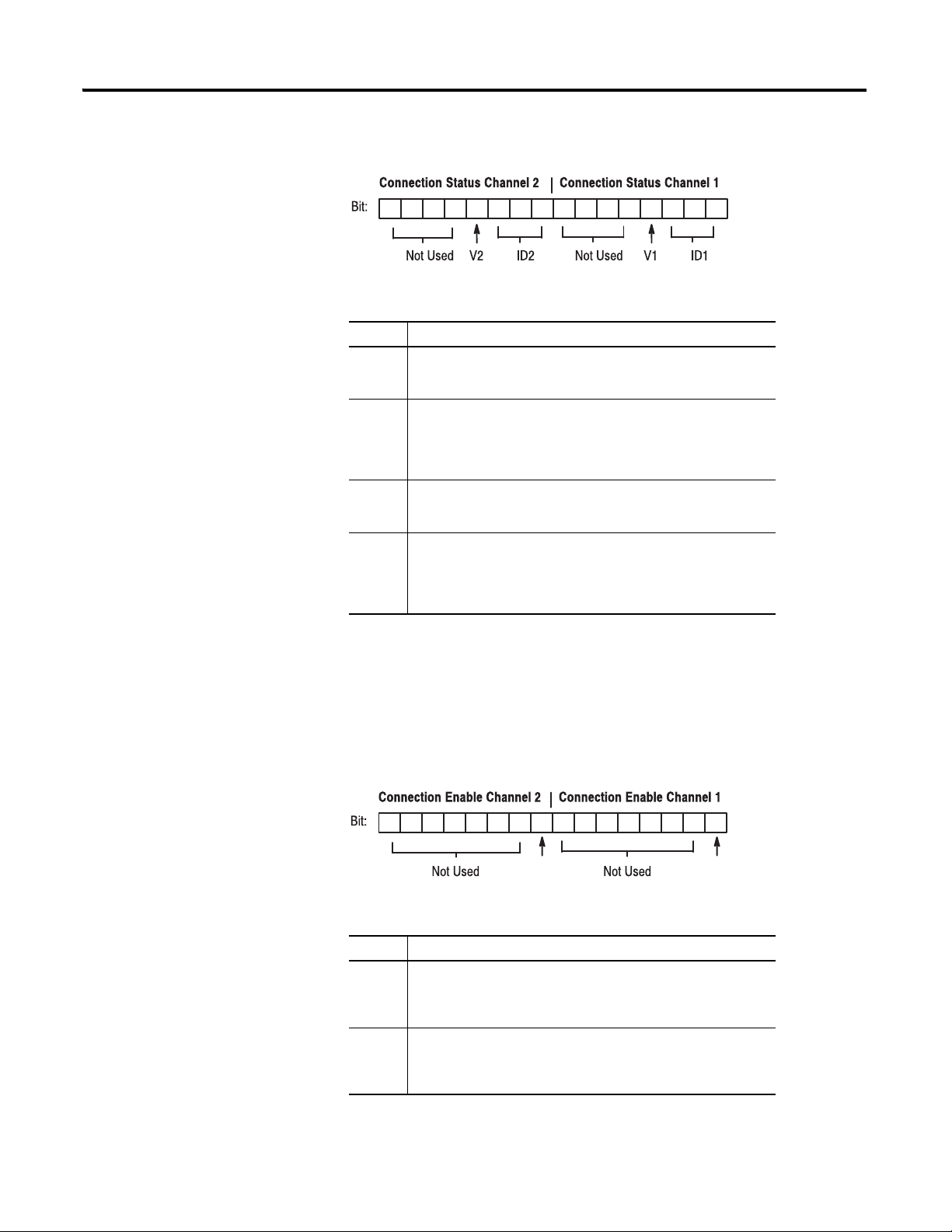
Communicate With Your Module 67
1153
1154
Connection Status Word Definition
3210765411 10 9 815 14 13 12
Connection Status Word Definitions
Descripton
V1 SCANport channel 1 valid data bit. When high (1), the Logic Status and
ID1 SCANport channel 1 connected peripheral port ID number. This three
V2 SCANport channel 2 valid data bit. When high (1), the Logic Status and
ID2 SCANport channel 2 connected peripheral port ID number. This three
Analog Feedback values are valid and can be used. When low (0), the
values should not be used.
bit field contains the port number that channel 1 is connected to on the
SCANport device. It should contain a value between 1 and 7. If this
field is 7, then the channel is not connected to the SCANport device or
the SCANport device may not be powered.
Analog Feedback values are valid and can be used. When low (0), the
values should not be used.
bit field contains the port number that channel 2 is connected to on the
SCANport device. It should contain a value between 1 and 7. If this
field is 7, then the channel is not connected to the SCANport device, or
the SCANport device may not be powered.
Logic Status/Analog Feedback Definition
The Logic State and Analog Feeback values are defined within the product
manuals of the connected SCANport device(s).
Connection Enable Word Definition
14 13 12
Connection Enabled Word Definitions
Descripton
E1 SCANport channel 1 enable bit. When set (1), the module attempts to
connect to the SCANport device. When reset (0), the module stops
communicating with the connected SCANport device. This usually
causes the device to fault.
E2 SCANport channel 2 enable bit. When set (1), the module attempts to
connect to the SCANport device. When reset (0), the module stops
communicating with the connected SCANport device. This usually
causes the device to fault.
32 10765411 10 9 815
E2 E1
Publication 1794-UM064B-EN-P - May 2014
Page 80

68 Communicate With Your Module
Logic Command/Analog Reference Definition
The Logic Command and Analog reference values are defined within the
product manuals of the connected SCANport device(s).
Defaults
Each I/O module has default values associated with it. At default, each module
generates inputs/status and expects outputs/configuration.
FLEX I/O Module Defaults
Module Defaults for: Adapter Defaults Optimal Sizes
Catalog Number Description Input
Default
1794-IB8 8-pt 24V DC Sink Input 1 1 1 0
1794-OB8 8-pt 24V DC Source Output 1 1 0 1
1794-IB16 16-pt 24V DC Sink Input 1 1 1 0
1794-OB16 16-pt 24V DC Source Output 1 1 0 1
1794-IV16 16-pt 24V DC Source Input 1 1 1 0
1794-OV16 16-pt 24V Sink Output 1 1 0 1
1794-OB8EP Elec. Prot. Output Module 1 1 0 1
1794-IB10XOB6 10 In/6 Out Combo Module 1 1 1 1
1794-IA8 8-pt 120V AC Input 1 1 1 0
1794-OA8 8-pt 120V AC Output 1 1 0 1
1794-IB8S 8-pt 24V DC Sensor Input 1 1 1 0
1794-OW8 8-pt Relay Output 1 1 0 1
1794-IE8 8-pt Analog Input 9 6 8 0
1794-OE4 4-pt Analog Output 1 14 0 4
1794-IE4XOE2 4 in/2 out Analog Combo 5 10 4 2
1794-IR8 8-pt RTD Analog Input 11 4 10 0
1794-IT8 8-pt Thermocouple Input 11 4 10 0
1794-IRT8 TC/mV/TRD Module 11 4 1 0
1794-IF4I 4 Isolated Input Module 7 5 1 0
1794-OF4I 4 Isolated Output Module 6 9 0 1
1794-IF2XOF2I Isolated Combo Module 7 7 1 1
1794-ID2 Incremental Encoder Module 8 7 1 0
1794-IP4 Pulse Counter Module 10 3 1 0
1203-FM1 SCANport Module 6 5 4 3
Output
Default
Input
Default
Output
Default
Publication 1794-UM064B-EN-P - May 2014
The default values refect the maximum number of read/write words.
You can change the I/O data size for a module by reducing the number of words
mapped into the adapter module, as shown in optimal sizes.
Page 81

Communicate With Your Module 69
Optimal sizes are the settings that provide optimal data to and from the I/O
modules. You need a software configuration tool to change the size. Make sure
the FLEX I/O adapter is compatible with the configuration tool you choose.
The optimal setting provide the fastest network time by only mapping read and
write words used by the I/O modules. If you reduce your data sizes to only
include optimal data, you can only change your configuration data with a
software tool. If you need to change configuration information on an optimal
basis, your data size must be large enough to include the necessary words.
Chapter Summary
In this chapter you learned how to communicate with your module. Read the
next chapter to learn how to connect to the PROFIBUS DP network.
Publication 1794-UM064B-EN-P - May 2014
Page 82

70 Communicate With Your Module
Notes:
Publication 1794-UM064B-EN-P - May 2014
Page 83

Chapter
3
Connect Your Adapter to the PROFIBUS DP Network
Overview
The DP Physical Layer
Read this chapter to install the input and output analog modules.
For Information On Page
The DP Physical Layer
Cabling and Equipment Required for Line A Type
Cabling and Equipment Required for Line B Type
Connect the Adapter to the Network
Terminate the Network
The PROFIBUS network media is a balanced transmission line corresponding to
the standard EIA RS-485, terminated at both ends. Both line A and line B types
are available, depending on your system requirements.
Specifications and guidelines for DP media:
• linear bus, terminated at both ends
• drop cables (preferably no longer than .30 m), no branches
• shielded twisted pair
• max. line length between 100 and 1200 m (depending on baudrate and
cable type)
•number of stations: 32
• DP baudrates: 9.6, 19.2, 93.75, 187.5, 500 Kbit/s, 1.5 Mbit/s, 12 MBd
71
72
73
74
76
Use the following table to determine what line type will best meet your needs.
Line Type Characteristics
Characteristic Bus Segments and Drop Cables
Line A Requirements
Impedance 135…165 Ω (3-29 MHz) 100…130 Ω (f> 100 kHz)
Capacity < 30 pF/m < 60 pF/m
Resistance < 110 Ω/km –
Wire Gauge > 0.64 mm > 0.53 mm
Conductor Area > 0.34 mm > 0.22 mm
71 Publication 1794-UM064B-EN-P - May 2014
(1)
(2)
Line B Requirements Total Capacity of
all Drop Cables
Page 84

72 Connect Your Adapter to the PROFIBUS DP Network
Line Type Characteristics
Characteristic Bus Segments and Drop Cables
Impedance 135…165 Ω (3-29 MHz) 100…130 Ω (f> 100 kHz)
Maximum
Length
with Baud
Rate
(bits/s) of:
Where: NA = Not Applicable
(1)
Measurements are the sum of all bus segments and drop cable lengths combined.
(2)
If using a combination of both line types, divide the lengths shown by two.
(1)
Line A Requirements
≤ 19.2 k1200 m 1200 m ≤ 15 nF
93.75 k 1200 m 1200 m ≤ 3 nF
187.5 k 1000 m 600 m ≤ 1 nF
500 k 400 m 200 m ≤ 0.6 nF
1.5 M 200 m NA ≤ 0.2 nF
12 M 100 m
(2)
Line B Requirements Total Capacity of
all Drop Cables
Cabling and Equipment Required for Line A Type
Line A cabling can support baudrates as high as 1.5 Mbits/s.
Cables
You need a shielded twisted pair cable for your cabling (bus segments or drop
cables). Any line A cable available on the market can be used to connect your
adapter to a PROFIBUS network.
T-junction Connectors
You need t-junction connectors to connect your droplines to bus segments. You
can use any t-junctions available on the market.
Termination Blocks
Termination blocks are only needed if the devices on the end of the network do
not have built-in terminating resistors. If you need termination blocks, you can
use any termination blocks available on the market.
Publication 1794-UM064B-EN-P - May 2014
Page 85

Connect Your Adapter to the PROFIBUS DP Network 73
IMPORTANT
IMPORTANT
Bus Connector
Connect your adapter to the PROFIBUS DP network by attaching a bus
connector to the female 9 pin D-Sub connector on the front of the module.
For detailed information on the topology and cabling for line A, refer
to the PROFIBUS Standard (DIN 19245 Parts 1 & 3, Issue 1994).
Cabling and Equipment Required for Line B Type
Line B cabling can support baudrates as high as 500 kbits/s.
Cables
You need a shielded twisted pair cable for your cabling (bus segments or drop
cables). Any shielded twisted pair cables available on the market can be used to
connect your adapter to a PROFIBUS network, however, bus segment cables
must contain wire for data ground and a cable braid shield. We recommend
Sprecher+Schuh cable as shown in the table below.
T-junction Connectors
You need T-junction connectors to connect your droplines to bus segments. You
can use any t-junctions available on the market, however, we recommend
Sprecher+Schuh connectors as shown in Tab l e
page 74.
Cable Types and Descriptions on
Termination Blocks
Termination blocks are only needed if the devices on the end of the network do
not have built-in terminating resistors. If you need to use termination blocks, any
termination blocks available on the market can be used, however, we recommend
Sprecher+Schuh termination blocks as shown in the table below.
Bus Connector
Connect your adapter to the PROFIBUS DP network by attaching a bus
connector to the female 9 pin D-Sub connector on the front of the module.
For detailed information on the topology and cabling for line B, refer
to the PROFIBUS Standard (DIN 19245 Parts 1 & 3, Issue 1994).
Publication 1794-UM064B-EN-P - May 2014
Page 86

74 Connect Your Adapter to the PROFIBUS DP Network
PROFIBUS DP
master/scanner
controller
PROFIBUS media
(trunk cable)
Other DP
adapter/slave
1794-APBDPV1 adapter/slave
FLEX I/O system
Other DP
adapter/slave
Personal computer
with configuration
software
1155
Cable Types and Descriptions
Equipment Type Catalog Number Part Number
Drop cable Sprecher + Schuh PTL-2, PTL-4, PDC-10 87.890.282-10
T-junction connector Sprecher + Schuh PTS-0 87.890.276-01
Bus segment cable Sprecher + Schuh none 299.257.001
Bus segment 1 m Sprecher + Schuh PCB-10 87.890.281-10
Connector Sprecher + Schuh none 87.890.283-01
Termination Block Sprecher + Schuh PCE-0 87.890.284-01
Connect the Adapter to the Network
For line A or B connections,
• use bus segments with t-junctions and termination blocks to form the
PROFIBUS media (trunk cable).
• Use termination blocks to terminate the line at each end of the trunk cable.
• Use drop cables to connect devices to the network.
The maximum number of stations on the same network is 32.
Publication 1794-UM064B-EN-P - May 2014
Connect Wiring to the Adapter
1. Connect the PROFIBUS drop cable to the 9-pin D-shell connector
according to the pin assignments in Ta b l e
page 75.
ATTENTION: If you connect or disconnect wiring while the field-side
power is on, an electrical arc can occur. This could cause an explosion in
hazardous location installations. Be sure that power is removed or the
area is nonhazardous before proceeding.
D-Shell Pin Assignment on
Page 87

Connect Your Adapter to the PROFIBUS DP Network 75
44558
G
E
24V
COM
PROFIBUS connector
D
F
44559
D-Shell Pin Assignment
PIN RS-485 Reference Signal Description
1 Shield Shield, RC to earth ground
2 RP Not used
3 B/B’ RXD/TXD-P Receive/transmit data - P
4 CTNR-P Not used
5 C/C’ DGND Data ground
6 VP Voltage plus (+5V)
7 PR Not used
8 A/A’ RXD/TXD-N Receive/transmit data - N
9 CTNR-N Not used
Metal shell Earth ground
2. Connect the cable shield to pin 1.
The shield is connected to earth ground.
3. Connect the data signal pins on both ends (signal + pin 3 and
signal - pin 8).
1
6
.
.
.
.
.
9
5
DROP CABLE
RCV/ Xmit data +
RCV/ Xmit data -
Earth ground
PROFIBUS
ADAPTER
Shield
Signal + Pin #3
Signal - Pin #8
Pin #1
Pin #5
*
Data ground
*
Pins #5 and #6 can be used to supply an external PROFIBUS terminator.
+5V Pin #6
4. Insert the wired connector into the mating connector on the PROFIBUS
adapter as shown.
Publication 1794-UM064B-EN-P - May 2014
Page 88

76 Connect Your Adapter to the PROFIBUS DP Network
PROFIBUS DP ADAPTER
.
.
.
.
+ 5V 6
3
8
5
390 Ω (2%, 1/4 W)
390 Ω (2%, 1/4 W)
CABLE
Signal +
Signal -
Data ground
220 Ω (2%, 1/4 W)
5
1
9
6
1157
5. Connect +V DC power to the left side of the lower connector, terminal E.
ATTENTION: Total power connection wire length must be less than
10 m (32.8 ft).
6. Connect - V common to the left side of the upper connector, terminal D.
7. Connections G and F are used to pass +V DC power (G) and -V common
(F) to the next module in the series (if required).
ATTENTION: When connecting wiring, torque terminal screws D, E, F,
and G to 0.8 Nm (7 lb-in).
ATTENTION: Do not wire more than two conductors on any single
terminal.
Terminate the Network
You must use termination blocks only if your devices on the end of the network
do not have built-in terminating resistors. Terminate the PROFIBUS media
(trunk cable) at both ends of the network. If you are not using a connector with
built-in resistors, terminate the cable at the adapter connector as shown.
Terminate at the Adapter Using Line A
Since Line A has a higher line impedance, you must use the following
termination resistors:
Publication 1794-UM064B-EN-P - May 2014
Page 89

Connect Your Adapter to the PROFIBUS DP Network 77
1158
Terminate at the Adapter Using Line B
Use the following termination resistors with line B:
Chapter Summary
PROFIBUS DP ADAPTER
+ 5V 6
Signal +
Signal -
Data ground
3
8
5
9
.
.
6
390 Ω (2%, 1/4 W)
150 Ω (2%, 1/4 W)
390 Ω (2%, 1/4 W)
5
.
.
1
CABLE
In this chapter you learned how to connect your adapter to the PROFIBUS DP
network. Read the next chapter to learn about how to configure your adapter for
Master/Slave communication
Publication 1794-UM064B-EN-P - May 2014
Page 90

78 Connect Your Adapter to the PROFIBUS DP Network
Notes:
Publication 1794-UM064B-EN-P - May 2014
Page 91

Chapter
Configure the Adapter for Master/Slave Communication
4
Overview
How Master/Slave Communication Takes Place
Read this chapter to familiarize yourself with input, output and configuration
files for analog I/O modules on the PROFIBUS network.
For Information On See Page
How Master/Slave Communication Takes Place 79
Enter User Parameter Data 80
Enter Check Configuration Data 86
A data exchange between the master and slave cannot be performed until check
configuration and send parameter data are issued. Each time you power-up the
network, the master sends check configuration and send parameter data to the
slave (FLEX I/O adapter).
Check configuration data determines or checks the number of input and output
words used by each FLEX I/O module.
Send parameter data contains device-specific parameters you define for each
FLEX I/O module.
You need a software configuration tool to set the values associated with these
parameters. Since the FLEX I/O adapter is compatible with any master, you can
use any compatible configuration tool available.
The Device Database File (GSD) is used by your configuration tool to help you
set up your system. Your configuration tool automatically reads the GSD file and
extracts defaults used in the data exchange. For more information on GSD files,
see Appendix B on page 105.
The file is in ASCII format and you can view it with any text editor. To download
a printable copy of your GSD file, see Appendix B on page 105.
The user parameter data fields are not defined in the GSD file. Depending on the
format you choose, you may have to manually edit these values with your
configuration tool.
For more information on how you define and enter these user parameter values,
refer to the documentation associated with your master and software
configuration tool.
79 Publication 1794-UM064B-EN-P - May 2014
Page 92

80 Configure the Adapter for Master/Slave Communication
GroupIdent.
Number
Minimum
Station
Delay
Watchdog
Control
Station
Status
User Parameter Data
Watchdog
Control
You configure these values using your
software configuration tool.
These values are defined by the PROFIBUS
standard. the defaults are provided by
the GSD file.
Ident.
1161
Enter User Parameter Data
Send parameter data is comprised of a string of octets (1…244) that contain 244
bytes of data:
• octets 1…7 contain data specific to the:
– PROFIBUS Standard
– defaults contained in the database (GSD) file
• octets 8…244 are user configurable and contain user parameter data. User
parameter data consists of these formats:
– auto configure
–condensed
–full
FigureSend Parameter Data Table Structure shows the structure of the send
parameter data table.
Send Parameter Data Table Structure
User Parameter Data
The first byte of the user parameter data is the flags byte. This byte selects the
appropriate format and also specifies adapter behavior. The flags byte is defined
in the following table:
Send Parameter Data Flags Byte
Bit Position Name Description
0…1 Format Selection 00 = Auto Configure
2…3 Fault Action 00 = Reset to zero
4 Input Fault Action 0 = Reset inputs to zero
5 Byte Order of Float values
6…7 Reserved Reserved bits must be zero
If the send parameter data is received with no user parameter data, the flags byte
is set to zero which selects:
01 = Reserved
10 = Condensed
11 = Full
01 = Hold Last State
10 = Use Safe State
11 = Reserved
1 = Hold Last Value
Publication 1794-UM064B-EN-P - May 2014
Page 93
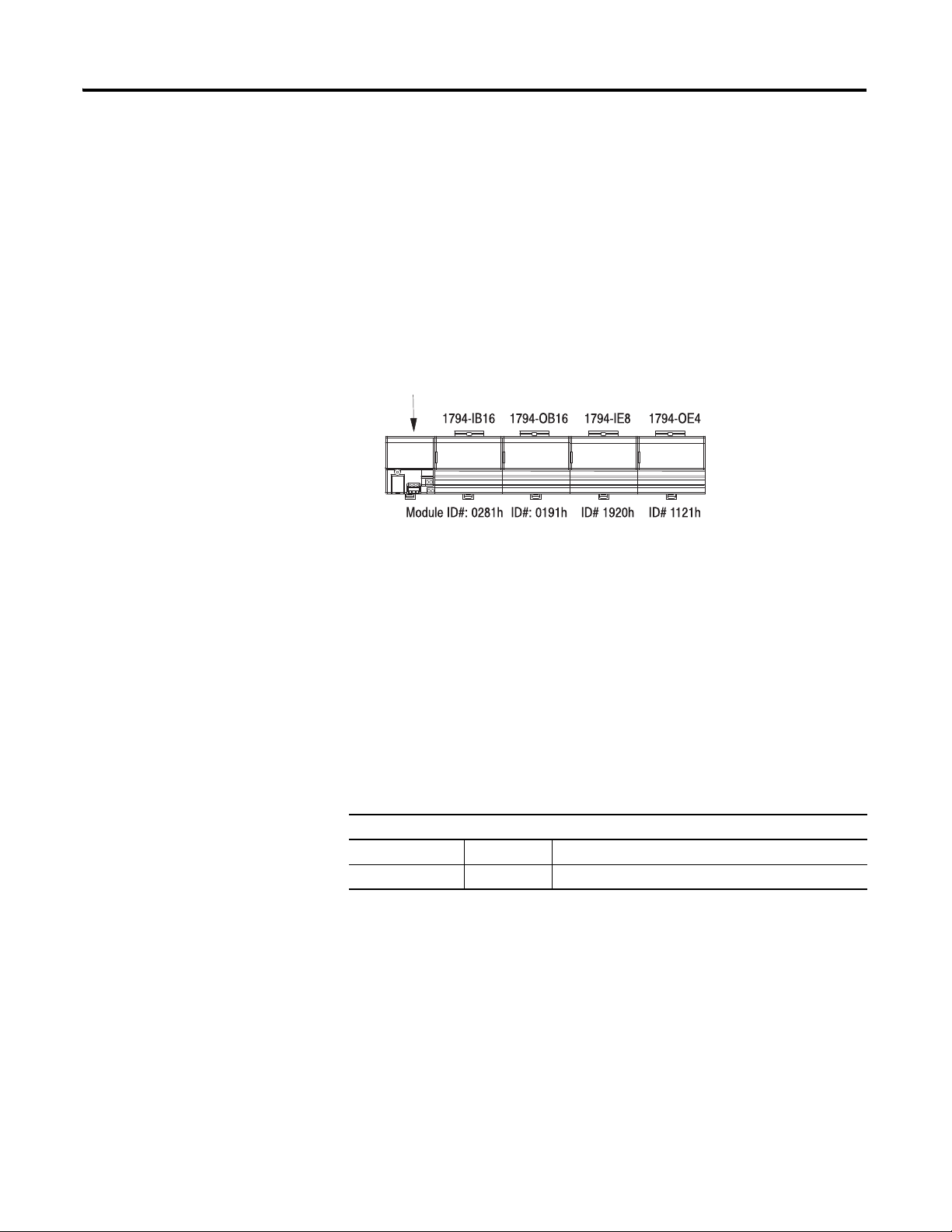
Configure the Adapter for Master/Slave Communication 81
1159
• auto configure
• reset outputs to zero on fault
• reset inputs to zero on fault
The reserved bits must be set to zero to prevent undesired firmware update
behavior. This is the default behavior of the module as defined in the GSD file.
The descriptions in this chapter use the following example FLEX I/O
configuration to explain the information required for each of these functions:
1794-APBDPV1 Adapter Slave
1794-APBDPV1 Adapter Slave
FLEX I/O System
Auto Configure Format
The Auto Configure format allows you to change modules without affecting the
User Parameter or Check Configuration data. This format provides no keying
from the master on the I/O modules installed in the FLEX I/O system. The
installed module at power-up is taken as the key.
If you change a module while it is being controlled by a master, a recoverable fault
occurs. To recover from this fault, you must replace the module with an identical
module type.
User Parameter Example
User Parameter Message, Auto Configure Format (Length 1 byte)
Name Value Description
Octet 8: 00h Auto Configure Format, Reset to Zero on Fault
The complete I/O module real time data table without the module ID, but with
the module configuration, is transferred via cyclic PROFIBUS data in one block.
Condensed Format
The condensed format consists of the flags byte and the module key parameter
for each of the eight slots. This parameter dictates which I/O module must be
installed. If at any time the actual module ID does not match this module key, the
slot will be considered in fault and the following occurs:
• Status Indicator flashes red/off
Publication 1794-UM064B-EN-P - May 2014
Page 94

82 Configure the Adapter for Master/Slave Communication
• an error bit in the poll response data is set
• a diagnostic bit in the Ext_Diag_Data field returned in the Read DP-Slave
All eight slots must be configured with the module key parameter. The size for
this format depends on the module types which are configured (1 word ID for
standar modules, 2 word ID for EDT modules). The range can vary from
20 bytes (including the flags byte) to 36 bytes.
The condensed format structure must be repeated for each of the eight slots.
Data Format for Condensed Format
Name Size Description
Module Key WORD Module ID # that must be installed
(1)
Only bits 0…12 are used. Bits 13…15 must be zero except when keying an empty slot where 0FFFFh is used.
The following table shows the identification numbers for commonly used FLEX
I/O modules.
Diagnostic Information message response is set
(1)
FLEX I/O Module Catalog Number Module Identification Number
Four-word Modules
1794-IB8 0180h
1794-OB8 0190h
1794-IB16 0281h
1794-OB16 0191h
1794-IV16 0204h
1794-OV16 010Ch
1794-IA8 0285h
1794-OA8 0195h
1794-OA8I 019Ch
1794-OW8 0199h
Sixteen-word Modules
1794-IE8/A 1920h
1794-OE4/A 1121h
1794-IE4XOE2/A 1522h
1794-IE8/B 1924h
1794-OE4/B 1125h
1794-IE4XOE2/B 1526h
1794-IT8 1B00h
1794-IR8 1B01h
1794-IRT8 1B03h
1794-ID2/B 1B03h
(module key)
Publication 1794-UM064B-EN-P - May 2014
Page 95

Configure the Adapter for Master/Slave Communication 83
FLEX I/O Module Catalog Number Module Identification Number
1794-IP4/B 1A04h
1203-FM1 1600h
1794-IE8H/A 1E3F 2003h
1794-OE8H/A 153F 2002h
1797-IE8H/A 1E3F 2001h
1797-OE8H/A 153F 2002h
1794-VHSC/A 1A3F 2000h
1794-IF8IH/A 1E3F 2005h
1794-OF8I/A 153F 2006h
1794-IE8H/B 1E3F 2103h
1794-OE8H/B 153F 2104h
1797-IE8H/B 1E3F 2102h
1797-OE8H/B 153F 2102h
(module key)
When you use the condensed format, no safe state data can be defined, thus the
safe state data is left at the power up default of all zeroes. Setting the Fault Action
in the byte to Use Safe State with this format is the equivalent of setting Reset to
Zero.
The complete I/O module real time data table without the module ID, but with
the module configuration, is transferred via cyclic PROFIBUS data in one block.
User Parameter Example
User Parameter Message, Condensed Format (Length 17 bytes)
Name Value Description
Octet 8: 02h Condensed Format, Reset to Zero on Fault, Reset
Octet 9-10: 0281h 1794-IB16 16-point discrete input module
Octet 11-12: 0191h 1794-OB16 16-point discrete output module
Octet 13-14: 1920h 1794-IE8 8-point analog input module
Octet 15-16: 1121h 1794-OE4 4-point analog output module
Octet 17-18: 0FFFFh Empty
Octet 19-20: 0FFFFh Empty
Octet 21-22: 0FFFFh Empty
Octet 23-24: 0FFFFh Empty
Inputs to Zero
Refer to your configuration tool publications for information on how and where
to enter this data.
Publication 1794-UM064B-EN-P - May 2014
Page 96

84 Configure the Adapter for Master/Slave Communication
Full Format
The full format consists of the flags byte and four parameters for each of the eight
slots. The module key parameter is the same for the full format as defined by the
condensed format, but adds three more parameters for each slot.
Use the full format for non EDT I/O modules to:
• provide Safe State values for output points
• send FLEX I/O module configurations once (when you send parameters)
• configure data sizes to reduce the size of data required during run mode
Use the full format for EDT I/O modules to:
• provide Safe State values for output points
• send FLEX I/O module configurations once (when you send parameters)
• configure data sizes to reduce the size of data required during run mode
• configure HART variables data to show in the cyclic PROFIBUS data
instead of every poll
instead of every poll
area.
You must configure all eight slots. The minimum size is 28 bytes – no slots have
FLEX I/O module configuration or safe state data. The maximum size is
237 bytes (the size of the PROFIBUS user parameter area).
Data Format for Full Format of Non EDT I/O Module
User
Parameter
Byte
5, 6 Module Key WORD Module ID # that must be installed
7 Module Data Sizes
8....x Safe State Data ARRAY Output Safe States. Word array of size Safe
x...y Module Configuration
(1)
Each of the two sizes can range from 0…15 words but when combined cannot exceed 15 words total.
(2)
Only bits 0…12 are used. Bits 13…15 must be zero except when keying an empty slot where 0xFFFF is used.
Name Size Description
(1)
BYTE Bits 0…3 Safe State Size (in words)
ARRAY FLEX I/O Module Configuration. Word array of
Data
Bits 4…7 Module Configuration Data Size (in
words)
State Size.
size Configuration Size.
(2)
Publication 1794-UM064B-EN-P - May 2014
Page 97

Configure the Adapter for Master/Slave Communication 85
Data Format for Full Format of EDT I/O Module
User
Name Size Description
Parameter
Byte
5...8 Module Key 2 WORDS Module ID # that must be installed
9 Module
Data Sizes
10 Configuratio
BYTE Bits 0…3 Safe State Size (in words)
(1)
Bits 4…7 Module Configuration Data Size (in words)
BYTE Module Configuration Data Size (in words)
(2)
n Data Sizes
11....X Safe State
ARRAY Output Safe States. Word array of size Safe State Size.
Data
X...Y Module
Configuratio
ARRAY FLEX Module Configuration. Word array of size
Configuration Size.
n Data
Y. . .Z H A R T
Variables
Configuratio
n
ARRAY Y.Byte Bits 0…3 HART loop select of first HART value
Y.Byte Bits 4…7 HART loop select of second HART value
Y+1.Byte Bits 0…3 HART loop select of third HART value
Y+1.Byte bits 4…7 HART loop select of fourth HART value
Y+2.Byte Bits 0…1 Variable select of first HART value
Y+2.Byte Bits 2…3 Variable select of seoncd HART value
Y+2.Byte Bits 4…5 Variable select of third HART value
Y+2.Byte Bits 6…7 Variable select of fourth HART value
(1)
Each of the two sizes can range from 0…15 words but when combined cannot exceed 15 words total.
(2)
Only bits 0…12 are used. Bits 13…15 must be zero except when keying an empty slot where 0xFFFF is used.
There are some possible configurations of FLEX I/O modules that would exceed
the user parameter area of 237 bytes. Be aware of the totals of the words and
modules you are using.
User Parameter Example
User Parameter Message, Full Format (Length 43 bytes)
Name Value Description
Octet 8: 02h Full Format, Reset to Zero on Fault
Octet 9…10: 0281h Slot 1 Module key 1794-IB16 16-point discrete input module
Octet 11: 10h Slot 1 config size 1 word, safe state size 0 words
Octet 12…13: 0000h 1 config word, input delay times
Octet 14…15: 0191h Slot 2 Module Key 1794-OB16 16-point discrete output module
Octet 16: 01h Slot 2 config size 0 words, safe state size 1 word
Octet 17…18: 0000h 1 safe state data word, safe state value for output points
Octet 19…20: 1920h Slot 3 Module Key 1794-IE8 8-point analog input module
Octet 21: 10h Slot 3 config size 1 word, safe state size 0 words
Octet 22…23: 0000h 1 config word, channel slection
Octet 24…25: 5121 Slot 4 Module Key 1794-OE4 4-point analog output module
Octet 26: 24h Slot 4 config size 2 words, safe state size 4 words
Octet 27…28: 0000h 2 config words – channel selection and
Octet 29…30: 0000h output enabled
Octet 31…32: 0000h 4 safe state data words – safe state size 4 words
Publication 1794-UM064B-EN-P - May 2014
Page 98

86 Configure the Adapter for Master/Slave Communication
User Parameter Example
User Parameter Message, Full Format (Length 43 bytes)
Name Value Description
Octet 33…34: 0000h output point 2
Octet 35…36: 0000h output point 3
Octet 37…38: 0000h output point 4
Octet 39…40: 0FFFFh Slot 5 empty
Octet 41: 00h Slot 5 all sizes zero
Octet 42…43 0FFFFh Slot 6 empty
Octet 44: 00h Slot 6 all sizes zero
Octet 45…46: 0FFFFh Slot 7 empty
Octet 47: 00h Slot 7 all sizes zero
Octet 48…49: 0FFFFh Slot 8 empty
Octet 50: 00h Slot 8 all sizes zero
Refer to your configuration tool publications for information on how and where
to enter this data.
Enter Check Configuration Data
On a PROFIBUS DP network, the I/O data exchanged between the
PROFIBUS DP master and a DP slave is encapsulated into logical modules. The
total I/O data exchanged between a PROFIBUS DP master and a DP slave
device comprises a set of logical modules which is defined in the check
configuration data.
Each physical slot of the FLEX I/O system is represented by two logical modules
(one input and one output). When the FLEX I/O adapter is powered-up, the
check configuration message configures the module format (input and output
words) and defines the size of the modules within the device. When the sizes are
configured, the I/O data can be optimized to remove unused data from the data
stream.
Both input and output sizes can be configured. If a slot is empty, or if either the
input or output module is zero length, the specific identifier for an empty module
(free place) must be used.
If the end of the identifiers is reached before all slots have been configured, the
remaining slots are configured as empty.
The first two modules allocated are for the adapter itself, and must always be a 1
word input module and a 1 word output module, regardless of what parameter
format you choose. The adapter uses these words for adapter status information.
Modules for each of the individual slots (FLEX I/O modules) must also follow
these word assignments.
Publication 1794-UM064B-EN-P - May 2014
Page 99

Configure the Adapter for Master/Slave Communication 87
Most Significant Bit
Bit Number
Consistency over
0 byte or word
1 whole length
length format
0 byte byte structure
1 word word structure
input/output
00 specific identifier formats
01 input
10 output
11 input-output
Length of data
00 1 byte resp. 1 word
15 16 byte resp. 16 words
76543210
Least Significant Bit
•
•
•
1160
The format of the adapter status word is defined in the following table:
Adapter Status Word
Input Status Word
Bit Position Name Description
0
1…7
8…15
Bit Position Name Description
0…15 Reserved sent as zeroes.
I/O Module Faults are caused by:
• transmission errors on the FLEX I/O backplane
• bad module
• removed module
• incorrect module inserted
Address Change This bit is set when the Node Address switch is
changed since power up.
Reserved Sent as zeroes.
I/O Module Fault This bit is set when an error is detected in a slot
position (bits 0…7 refer to slots 1…8).
Output Status Word
The adapter expects the identifier area for each of the eight FLEX I/O slots to be
2 bytes. The DP input/output identifier and all specific DP identifiers (except
the empty module) are not supported.
The identifier byte and its format are described in the following illustration. This
byte is defined in Part 3 of the PROFIBUS Standard.
Publication 1794-UM064B-EN-P - May 2014
Page 100

88 Configure the Adapter for Master/Slave Communication
The maximum size of this identifier area is 17 bytes. If no FLEX I/O modules are
installed in the upper slots, the length may be less. Consistency must be over a
word.
Check Configuration Example
Check Configuration Message when used with Send Parameter Auto Configure or
Condensed Format (Length 10 bytes)
Name Identifier Byte Description
Octet 1: 50h Input Status Word (input – 1 word)
Octet 2: 60h Output Status Word (output – 1 word)
Octet 3: 51h Slot 1, input module 2 words
Octet 4: 60h Slot 1, output module 1 word
Octet 5: 00h Slot 2, input module empty
Octet 6: 60h Slot 2, output module 1 word
Octet 7: 57h Slot 3, input module 8 words
Octet 8: 60h Slot 3, output module 1 word
Octet 9: 50h Slot 4, input module empty
Octet 10: 65h Slot 4, output module 6 words
I/O sizes configured: 22 input bytes, 20 output bytes
Refer to your configuration tool publications for information on how and where
to enter this data.
Check Configuration Example
Check Configuration Message when used with Send Parameter Full Format
(Length 10 bytes)
Name Identifier Byte Description
Octet 1: 50h Status Word (input – 1 word)
Octet 2: 60h Output Status Word (output – 1 word)
Octet 3: 51h Slot 1, input module 2 words
Octet 4: 00h Slot 1, output module 1 word
Octet 5: 00h Slot 2, input module empty
Octet 6: 60h Slot 2, output module 1 word
Octet 7: 57h Slot 3, input module 8 words
Octet 8: 00h Slot 3, output module 1 word
Octet 9: 00h Slot 4, input module empty
Octet 10: 63h Slot 4, output module 6 words
I/O sizes configured: 22 input bytes, 12 output bytes
Refer to your configuration tool publications for information on how and where
to enter this data.
Publication 1794-UM064B-EN-P - May 2014
 Loading...