

Page 1

Allen-Bradley
FLEX Integra Analog
Modules
(Cat. No. 1793-IE4, -IE4S, -OE2,
-OE2S, -IE2XOE1 and -IE2XOE1S)
User Manual
Page 2

Important User Information
Because of the variety of uses for the products described in this publication,
those responsible for the application and use of this control equipment must
satisfy themselves that all necessary steps have been taken to assure that
each application and use meets all performance and safety requirements,
including any applicable laws, regulations, codes and standards.
The illustrations, charts, sample programs and layout examples shown in
this guide are intended solely for purposes of example. Since there are many
variables and requirements associated with any particular installation,
Allen-Bradley does not assume responsibility or liability (to include
intellectual property liability) for actual use based upon the examples shown
in this publication.
Allen-Bradley publication SGI-1.1, Safety Guidelines for the Application,
Installation and Maintenance of Solid-State Control (available from your
local Allen-Bradley office), describes some important differences between
solid-state equipment and electromechanical devices that should be taken
into consideration when applying products such as those described in this
publication.
Reproduction of the contents of this copyrighted publication, in whole or
part, without written permission of Rockwell Automation, is prohibited.
Throughout this manual we use notes to make you aware of safety
considerations:
ATTENTION: Identifies information about practices or
circumstances that can lead to personal injury or death,
property damage or economic loss
Attention statements help you to:
• identify a hazard
• avoid a hazard
• recognize the consequences
Important: Identifies information that is critical for successful application
and understanding of the product.
DeviceNetManager, Allen-Bradley, FLEX I/O and FLEX Integra are trademarks of Rockwell Automation
ControlNet is a trademark of ControlNet International.
DeviceNet is a trademark of Open DeviceNet Vendor Association, Inc.
Page 3

Preface
Using This Manual
Purpose of this Manual This manual shows you how to use your FLEX Integra Analog modules
with Allen-Bradley programmable controllers. The manual helps you
install, program and troubleshoot your modules.
Audience You must be able to program and operate an Allen-Bradley programmable
controller to make efficient use of your FLEX Integra modules. In
particular, you must know how to program block transfers, and be familiar
with DeviceNet or ControlNet software.
Vocabulary We assume that you know how to do this in this manual. If you do not, refer
to the appropriate programming and operations manual before you attempt
to program your modules.
In this manual, we refer to:
– the analog input or analog output module as the “input module” or
“output module”
– the Programmable Controller as the “controller”
Manual Organization This manual is divided into five chapters. The following chart lists each
chapter with its corresponding title and a brief overview of the topics
covered in that chapter.
Chapter Title Contents
1 Overview of FLEX Integra and
Analog modules
2 How to Install Your Analog Module How to install and wire the modules
3 Module Programming Explains block transfer programming, sample programs
4 Writing Configuration to and
Reading Status From with a
Remote I/O Adapter
5 How Communication Takes Place
and I/O Image Table Mapping with
the DeviceNet Adapter
6 Input, Status, Output and
Configuration with ControlNet
Appendix Title Contents
A Specifications Specifications for the analog modules
Describes FLEX Integra Analog modules, features, and how
they function
Explains how to configure your modules and read status
information from your modules when using a remote I/O
adapter
Explains how you communicate with your modules, and
how the I/O image is mapped when using a DeviceNet
adapter
Explains how you communicate with your modules, and
how the I/O image is mapped when using ControlNet.
Publication 1793-6.5.1 - April 1999
Page 4
P-2 Using This Manual
Conventions We use these conventions in this manual:
In this manual, we show: Like this:
that there is more information about a topic
in another chapter in this manual
that there is more information about the topic
in another manual
For Additional Information For additional information on FLEX Integra and FLEX I/O systems and
modules, refer to the following documents:
Catalog
Number
1793 Series
1793-IB4 4 Input Module 1793-5.1
1793-OB4P
1793-IB2XOB2P
1793-IE4 24V dc 4 Input Analog Module 1793-5.4
1793-IE2XOE1P 24V dc 2 In/1 Protected Output Analog Module 1793-5.6
1793-OW4
1794 1794 FLEX I/O Product Data 1794-2.1
1794-ACN 24V dc ControlNet Adapter 1794-5.8
1794-ACNR 24V dc Redundant Media ControlNet Adapter 1794-5.18
1794-ACN15 24V dc ControlNet Adapter 1794-5.47
1794-ACNR15 24V dc Redundant Media ControlNet Adapter 1794-5.48
1794-ADN 24V dc DeviceNet Adapter 1794-5.14 1794-6.5.5
1794-ASB/C & D 24V dc Remote I/O Adapter 1794-5.50 1794-6.5.9
1794-ASB2/B 24V dc 2-Slot Remote I/O Adapter 1794-5.44 1794-6.5.13
1794-APB 24V dc Profibus Adapter 1794-5.40 1794-6.5.6
1794-IB8 24V dc 8 Sink Input Module 1794-5.30
1794-OB8 24V dc 8 Source Output Module 1794-5.31
1794-IB16 24V dc 16 Sink Input Module 1794-5.4
1794-OB16 24V dc 16 Source Output Module 1794-5.3
1794-IV16 24V dc 16 Source Input Module 1794-5.28
1794-OV16 24V dc 16 Sink Output Module 1794-5.29
1794-OB8EP 24V dc 8 Electronically Fused Output Module 1794-5.20
1794-IB8S 24V dc Sensor Input Module 1794-5.7
Voltage Description
FLEX Integra Product Data 1793-2.1
4 Protected Output Module 1793-5.2
2 In/2 Protected Output Module 1793-5.3
4 Relay Output Module 1793-5.7
Publications
Installation
Instructions
User
Manual
1791-6.5.11793-OE2 24V dc 2 Protected Output Analog Module 1793-5.5
Publication 1793-6.5.1 - April 1999
Table continued on next page
Page 5

Using This Manual P-3
Catalog
Number
1794-IB10XOB6 24V dc 10 Input/6 Output Module 1794-5.24
1794-IE8 24V dc Selectable Analog 8 Input Module 1794-5.6 1794-6.5.2
1794-OE4 24V dc Selectable Analog 4 Output Module 1794-5.5
1794-IE4XOE2 24V dc 4 Input/2 Output Analog Module 1794-5.15
1794-OF4 24V dc 4 Output Isolated Analog Module 1794-5.37
1794-IF2XOF2 24V dc 2 Input/2 Output Isolated Analog Module 1794-5.39
1794-IR8 24V dc 8 RTD Input Analog Module 1794-5.22 1794-6.5.4
1794-IT8 24V dc 8 Thermocouple Input Module 1794-5.21 1794-6.5.7
1794-IRT8 24V dc 8 Thermocouple/RTD Input Module 1794-5.50 1794-6.5.12
1794-IJ2 24V dc 2 Frequency Input Module 1794-5.49 1794-6.5.11
1794-ID2 24V dc 2 Input Incremental Encoder Module 1794-5.63 1794-6.5.15
1794-IP4 24V dc 4 Input Pulse Counter Module 1794-5.64 1794-6.5.16
1794-VHSC 24V dc Very High Speed Counter Module 1794-5.67 1794-6.5.10
1794-IA8 120V ac 8 Input Module 1794-5.9
1794-OA8 120V ac Output Module 1794-5.10
1794-TB2
1794-TB3
1794-TBN Terminal Base Unit 1794-5.16
1794-TBNF Fused Terminal Base Unit 1794-5.17
1794-TB3T Temperature Terminal Base Unit 1794-5.41
1794-TB3S Spring Clamp Terminal Base Unit 1794-5.42
1794-TB3TS Spring Clamp Temperature Base Unit 1794-5.43
1794-TB3G Terminal Base Unit 1794-5.51
1794-TB3GS Spring Clamp Terminal Base Unit 1794-5.59
1794-CE1, -CE3 Extender Cables 1794-5.12
1794-NM1 Mounting Kit 1794-2.13
1794-PS1 24V dc Power Supply 1794-5.35
Voltage Description
2-wire Terminal Base
3-wire Terminal Base
Publications
Installation
Instructions
1794-5.2
User
Manual
1794-6.5.81794-IF4 24V dc 4 Input Isolated Analog Module 1794-5.38
Publication 1793-6.5.1 - April 1999
Page 6

Using This Manual
How to Install Your Analog
Module
Table of Contents
Preface
Purpose of this Manual . . . . . . . . . . . . . . . . . . . . . . . . . . . . . . . . . P-1
Audience . . . . . . . . . . . . . . . . . . . . . . . . . . . . . . . . . . . . . . . . . . . . P-1
Vocabulary . . . . . . . . . . . . . . . . . . . . . . . . . . . . . . . . . . . . . . . . . . P-1
Manual Organization . . . . . . . . . . . . . . . . . . . . . . . . . . . . . . . . . . P-1
Conventions . . . . . . . . . . . . . . . . . . . . . . . . . . . . . . . . . . . . . . . . . P-2
For Additional Information . . . . . . . . . . . . . . . . . . . . . . . . . . . . . P-2
Table of Contents
Chapter Objectives . . . . . . . . . . . . . . . . . . . . . . . . . . . . . . . . . . . . 2-1
Before You Install Your
Analog Module . . . . . . . . . . . . . . . . . . . . . . . . . . . . . . . . . . . . . . . 2-1
Compliance to
European Union Directives . . . . . . . . . . . . . . . . . . . . . . . . . . . . . 2-1
EMC Directive . . . . . . . . . . . . . . . . . . . . . . . . . . . . . . . . . . . . 2-1
Low Voltage Directive . . . . . . . . . . . . . . . . . . . . . . . . . . . . . . 2-2
Power Requirements. . . . . . . . . . . . . . . . . . . . . . . . . . . . . . . . . . . 2-2
Installing the Module . . . . . . . . . . . . . . . . . . . . . . . . . . . . . . . . . . 2-2
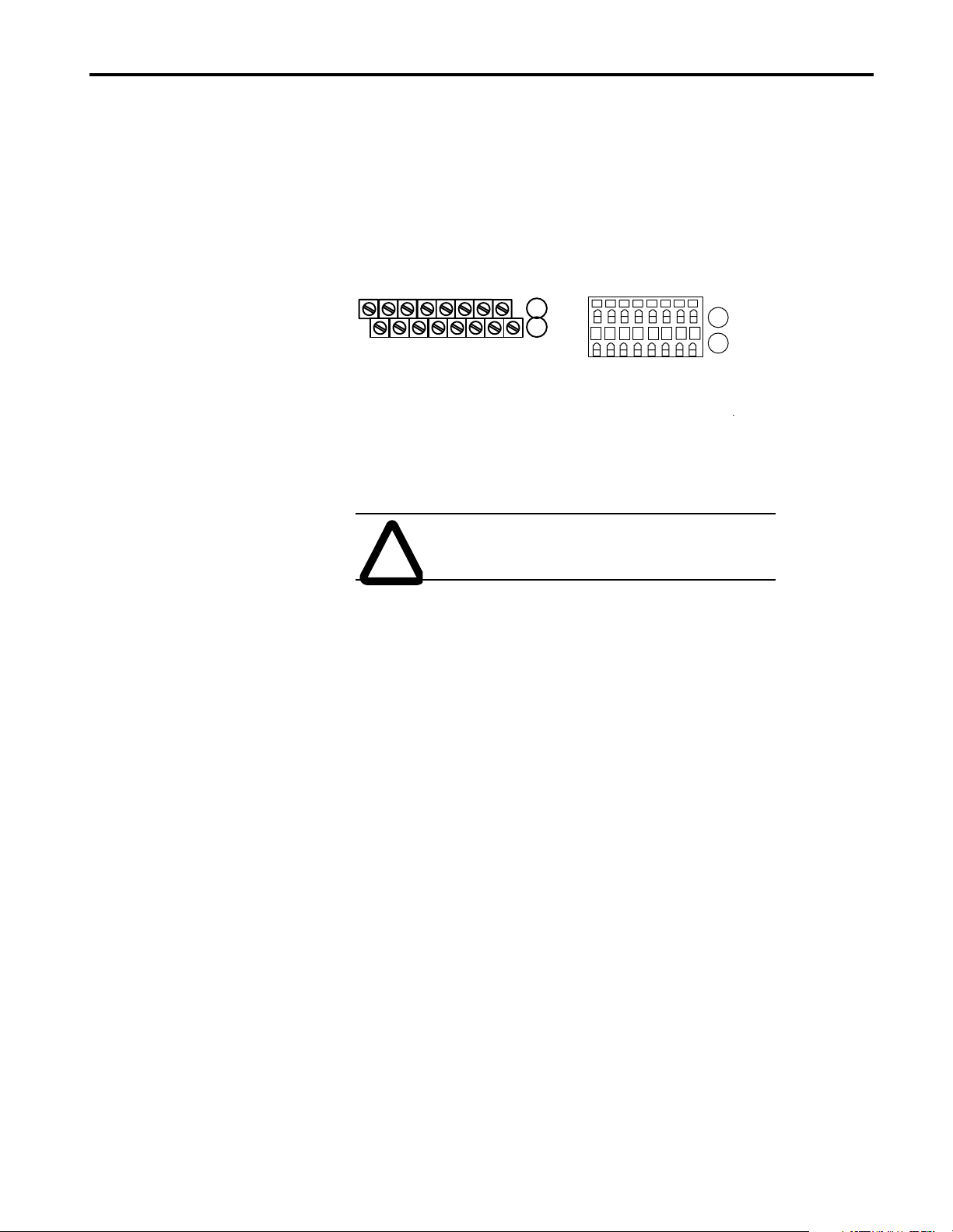
Connecting Wiring for the Analog Modules . . . . . . . . . . . . . . . . 2-5
Connecting Wiring for the 1793-IE4 Input Module. . . . . . . . 2-5
Connecting Wiring for the 1793-OE2 Output Module. . . . . . 2-6
Connecting Wiring for the 1793-IE2XOE1 Input/Output
Module . . . . . . . . . . . . . . . . . . . . . . . . . . . . . . . . . . . . . . . . . . 2-8
Module Indicators. . . . . . . . . . . . . . . . . . . . . . . . . . . . . . . . . . . . 2-10
Chapter Summary . . . . . . . . . . . . . . . . . . . . . . . . . . . . . . . . . . . . 2-10
Module Programming
Chapter 3
Chapter Objectives . . . . . . . . . . . . . . . . . . . . . . . . . . . . . . . . . . . . 3-1
Block Transfer
Programming . . . . . . . . . . . . . . . . . . . . . . . . . . . . . . . . . . . . . . . . 3-1
Sample programs for FLEX Integra Analog Modules . . . . . . . . . 3-2
PLC-3 Programming. . . . . . . . . . . . . . . . . . . . . . . . . . . . . . . . 3-2
PLC-5 Programming. . . . . . . . . . . . . . . . . . . . . . . . . . . . . . . . 3-4
PLC-2 Programming. . . . . . . . . . . . . . . . . . . . . . . . . . . . . . . . 3-5
Analog Data Format . . . . . . . . . . . . . . . . . . . . . . . . . . . . . . . . . . . 3-5
Chapter Summary . . . . . . . . . . . . . . . . . . . . . . . . . . . . . . . . . . . . . 3-6
Publication 1793-6.5.1 - April 1999
Page 7

ii
Writing Configuration to and
Reading Status from Your
Module with a Remote I/O
Adapter
Chapter 4
Chapter Objectives . . . . . . . . . . . . . . . . . . . . . . . . . . . . . . . . . . . . 4-1
Configuring Your Analog Module . . . . . . . . . . . . . . . . . . . . . . . . 4-1
Range Selection. . . . . . . . . . . . . . . . . . . . . . . . . . . . . . . . . . . . . . . 4-2
Safe State Value Selection . . . . . . . . . . . . . . . . . . . . . . . . . . . . . . 4-2
Data Format. . . . . . . . . . . . . . . . . . . . . . . . . . . . . . . . . . . . . . . . . . 4-2
Reading Data From Your Module . . . . . . . . . . . . . . . . . . . . . . . . 4-2
Mapping Data for the Analog Modules . . . . . . . . . . . . . . . . . . . . 4-2
Analog Input Module (1793-IE4 and -IE4S) Read . . . . . . . . . 4-3
Word/Bit Descriptions for the 1793-IE4 and -IE4S Analog Input
Module Read . . . . . . . . . . . . . . . . . . . . . . . . . . . . . . . . . . . . . . 4-4
Analog Input Module (1793-IE4 and -IE4S) Write
Configuration Block . . . . . . . . . . . . . . . . . . . . . . . . . . . . . . . . . 4-4
Range Selection Bits for the 1793-IE4 and -IE4S Analog
Input Module . . . . . . . . . . . . . . . . . . . . . . . . . . . . . . . . . . . . . . 4-5
Word/Bit Descriptions for the 1793-IE4 and -IE4S Analog Input
Module Write . . . . . . . . . . . . . . . . . . . . . . . . . . . . . . . . . . . . . 4-5
Analog Output Module (1793-OE2 and -OE2S) Read . . . . . . 4-6
Bit/Word Descriptions for the 1793-OE2 and -OE2S Analog
Output Module Read . . . . . . . . . . . . . . . . . . . . . . . . . . . . . . . . 4-6
Analog Output Module (1793-OE2 and -OE2S) Write
Configuration Block . . . . . . . . . . . . . . . . . . . . . . . . . . . . . . . . . 4-6
Range Selection Bits for the 1793-OE2 and -OE2S Analog Output
Module (Word 5) . . . . . . . . . . . . . . . . . . . . . . . . . . . . . . . . . . . 4-7
Word/Bit Descriptions for the 1793-OE2 and -OE2S Analog
Output Module Write . . . . . . . . . . . . . . . . . . . . . . . . . . . . . . . . 4-7
Analog Combo Module (1793-IE4XOE1) Read . . . . . . . . . . . 4-8
Word/Bit Descriptions for the 1794-IE4XOE1 and -IE2XOE1S
Analog Combo Module Read . . . . . . . . . . . . . . . . . . . . . . . . . 4-8
Analog Combo Module (1793-IE2XOE1 and -IE2XOE1S) Write
Configuration Block . . . . . . . . . . . . . . . . . . . . . . . . . . . . . . . . . 4-9
Range Selection Bits for the 1793-IE2XOE1 and -IE2XOE1S
Analog Combo Module . . . . . . . . . . . . . . . . . . . . . . . . . . . . . 4-10
Word/Bit Descriptions for the 1793-IE2XOE1 and -IE2XOE1S
Analog Combo Module Write . . . . . . . . . . . . . . . . . . . . . . . . 4-10
Chapter Summary . . . . . . . . . . . . . . . . . . . . . . . . . . . . . . . . . . . . 4-11
How Communication Takes
Place and I/O Image Table
Mapping with the DeviceNet
Adapter
Publication 1793-6.5.1 - April 1999
Chapter 5
Chapter Objectives . . . . . . . . . . . . . . . . . . . . . . . . . . . . . . . . . . . . 5-1
About DeviceNetManager
Software . . . . . . . . . . . . . . . . . . . . . . . . . . . . . . . . . . . . . . . . . . . . 5-1
Polled I/O Structure . . . . . . . . . . . . . . . . . . . . . . . . . . . . . . . . . . . 5-1
System Throughput . . . . . . . . . . . . . . . . . . . . . . . . . . . . . . . . . . . . 5-3
Mapping Data into the
Image Table. . . . . . . . . . . . . . . . . . . . . . . . . . . . . . . . . . . . . . . . . . 5-3
Defaults . . . . . . . . . . . . . . . . . . . . . . . . . . . . . . . . . . . . . . . . . . . . 5-11
Chapter Summary . . . . . . . . . . . . . . . . . . . . . . . . . . . . . . . . . . . . 5-12
Page 8

Input, Status, Output and
Configuration Files using
ControlNet
iii
Chapter 6
What this Chapter Contains . . . . . . . . . . . . . . . . . . . . . . . . . . . . . 6-1
About the ControlNet Adapter . . . . . . . . . . . . . . . . . . . . . . . . . . . 6-1
Communication Over the
FLEX I/O Backplane . . . . . . . . . . . . . . . . . . . . . . . . . . . . . . . . . . 6-1
Scheduled Data-Transfer . . . . . . . . . . . . . . . . . . . . . . . . . . . . 6-2
Unscheduled Data-Transfer . . . . . . . . . . . . . . . . . . . . . . . . . . 6-2
Module I/O Mapping . . . . . . . . . . . . . . . . . . . . . . . . . . . . . . . 6-2
I/O Structure . . . . . . . . . . . . . . . . . . . . . . . . . . . . . . . . . . . . . . . . . 6-3
Adapter Input Status Word . . . . . . . . . . . . . . . . . . . . . . . . . . . 6-3
Safe State Data . . . . . . . . . . . . . . . . . . . . . . . . . . . . . . . . . . . . . . . 6-4
Device Actions . . . . . . . . . . . . . . . . . . . . . . . . . . . . . . . . . . . . . . . 6-4
Communication Fault Behavior . . . . . . . . . . . . . . . . . . . . . . . 6-5
Idle State Behavior . . . . . . . . . . . . . . . . . . . . . . . . . . . . . . . . . 6-5
Input Data Behavior upon Module Removal . . . . . . . . . . . . . 6-5
Input Word/Bit Descriptions for the 1793-IE4 and -IE4S Analog
Input Module . . . . . . . . . . . . . . . . . . . . . . . . . . . . . . . . . . . . . 6-6
Range Selection Bits for the 1793-IE4 and -IE4S Analog Input
Module . . . . . . . . . . . . . . . . . . . . . . . . . . . . . . . . . . . . . . . . . . . 6-7
Configuration Word/Bit Descriptions for the 1793-IE4 and -IE4S
Analog Input Module . . . . . . . . . . . . . . . . . . . . . . . . . . . . . . . 6-7
ABit/Word Descriptions for the 1793-OE2 and -OE2S Analog
Output Module Read . . . . . . . . . . . . . . . . . . . . . . . . . . . . . . . . 6-8
Range Selection Bits for the 1793-OE2 and -OE2S Analog
Output Module (Word 5) . . . . . . . . . . . . . . . . . . . . . . . . . . . . . 6-8
Output Word/Bit Descriptions for the 1793-OE2 and -OE2S
Analog Output Module Write . . . . . . . . . . . . . . . . . . . . . . . . . 6-8
Configuration Word/Bit Descriptions for the 1793-OE2 and
-OE2S Analog Output Module Write . . . . . . . . . . . . . . . . . . . 6-9
Input Word/Bit Descriptions for the 1793-IE2XOE1and
-IE2XOE1S Analog Combo Module . . . . . . . . . . . . . . . . . . . 6-9
Range Selection Bits for the 1793-IE2XOE1and -IE2XOE1S
Analog Combo Module . . . . . . . . . . . . . . . . . . . . . . . . . . . . . 6-10
Output Word/Bit Descriptions for the 1793-IE2XOE1and
-IE2XOE1S Analog Combo Module . . . . . . . . . . . . . . . . . . 6-10
Chapter Summary . . . . . . . . . . . . . . . . . . . . . . . . . . . . . . . . . . . . 6-11
Specifications
Data Table Formats
Appendix A
Specifications . . . . . . . . . . . . . . . . . . . . . . . . . . . . . . . . . . . . . . . . A-1
Appendix B
Two’s Complement Binary . . . . . . . . . . . . . . . . . . . . . . . . . . . . . B-1
Analog Data Format . . . . . . . . . . . . . . . . . . . . . . . . . . . . . . . . . . . B-2
Publication 1793-6.5.1 - April 1999
Page 9
Chapter
1
Overview of FLEX Integra and your
Analog Modules
Chapter Objectives In this chapter, we tell you about:
• what the FLEX Integra system is and what it contains
• types of FLEX Integra analog modules
• how FLEX Integra analog modules communicate with programmable
controllers
• the features of your analog modules
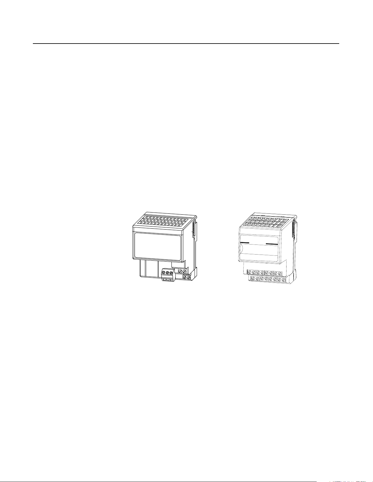
The FLEX Integra System FLEX Integra is a small, modular I/O system for distributed applications
that performs all of the functions of rack-based I/O. The FLEX Integra
system contains the following components shown below:
Adapter
Flexbus connector
Remote I/O
Connector
• adapter/power supply – powers the internal logic for as many as eight
• I/O module with integral wiring terminals– contains the bus interface
24V dc field power
connection terminals
(externally provided)
I/O modules
and circuitry needed to perform specific functions related to your
application and connection terminals for connecting wiring.
Integra Module
Flexbus connector
Field wiring terminals
41480
Publication 1793-6.5.1 - April 1999
Page 10
1-2 Overview of FLEX Integra and your Analog Modules
Types of FLEX Integra Modules We describe the following FLEX Integra Analog modules in this user
manual:
Catalog Number Voltage Inputs Outputs Description
1793-IE4 24V dc 4 –
1793-IE4S 24V dc 4 –
1793-OE2 24V dc – 2
1793-OE2S 24V dc – 2
1793-IE2XOE1 24V dc 2 1
1793-IE2XOE1S 24V dc 2 1
FLEX Integra analog input, output and combination modules are block
transfer modules that interface analog signals with any Allen-Bradley
programmable controllers that have block transfer capability. Block
transfer programming moves input from the module’s memory to a
designated area in the processor data table, and output data words from a
designated area in the processor data table to the module’s memory. Block
transfer programming also moves configuration words from the processor
data table to module memory.
analog – 4 input, single-ended, non-isolated;
screw-cage connectors
analog – 4 input, single-ended, non-isolated;
spring-clamp connectors
analog – 2 output, single-ended, non-isolated;
screw-cage connectors
analog – 2 output, single-ended, non-isolated;
spring-clamp connectors
analog – 2 input, single-ended, non-isolated
and 1 output, single-ended, non-isolated;
screw-cage connectiors
analog – 2 input, single-ended, non-isolated
and 1 output, single-ended, non-isolated;
spring-clamp connectors
How FLEX Integra Analog
Modules Communicate with
Programmable Controllers
The analog modules have selectable ranges as shown in the table below:
Voltage Current
0 to 10V dc 0 to 20mA
±10V dc 4 to 20mA
The adapter/power supply transfers data to the module (block transfer
write) and from the module (block transfer read) using BTW and BTR
instructions in your ladder diagram program. These instructions let the
adapter obtain input values and status from the module, and let you send
output values and establish the module’s mode of operation. Figure 1.1
describes the communication process.
Publication 1793-6.5.1 - April 1999
Page 11
Overview of FLEX Integra and your Analog Modules 1-3
Figure 1.1
An Example of Communication Between an Adapter and an
Analog Input Module
ADAPTER
ACTIVE FAULT
Allen-Bradley
LOCAL
FAULT
1
The adapter transfers your configuration data
to the module using a BTW.
Flexbus
POWER SUPPLY
RIO ADAPTER
24VDC
1794-ASB
4
Your ladder program instructs the
adapter to perform a BTR of the values
and stores them in a data table.
5
The adapter and module determine
that the transfer was made without error
and input values are within specified
range.
6
Your ladder program can use and/or move the data
(if valid) before it is written over by the transfer of
new data in a subsequent transfer.
2
External devices transmit
analog signals to the module.
Allen-Bradley
3
The module converts analog signals
into binary format and stores these
values until the adapter requests their
transfer.
7
Your ladder program performs BTWs to the module when
you power it up, and any time you wish to reconfigure the module.
Publication 1793-6.5.1 - April 1999
Page 12
1-4 Overview of FLEX Integra and your Analog Modules
Features of your Analog
Modules
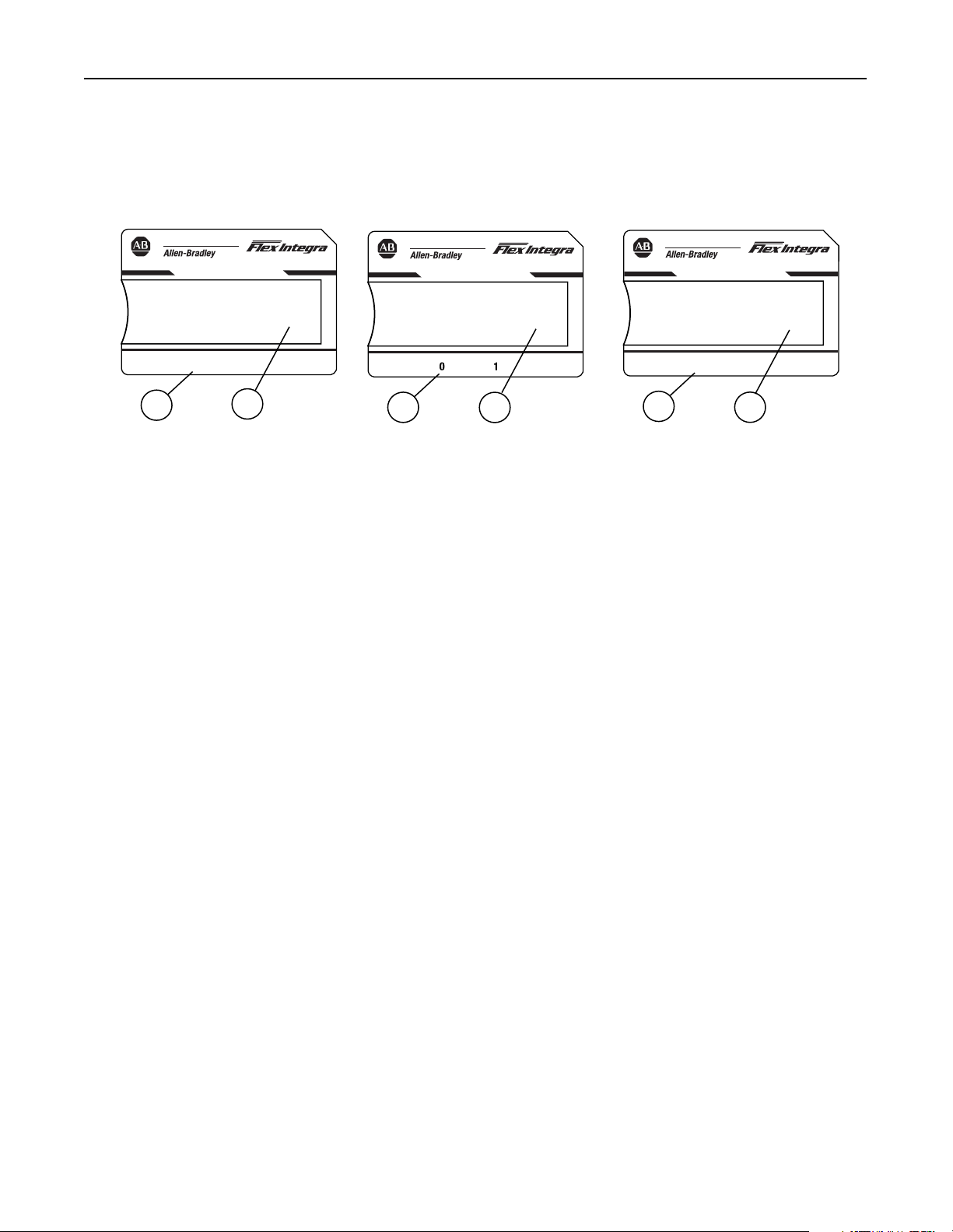
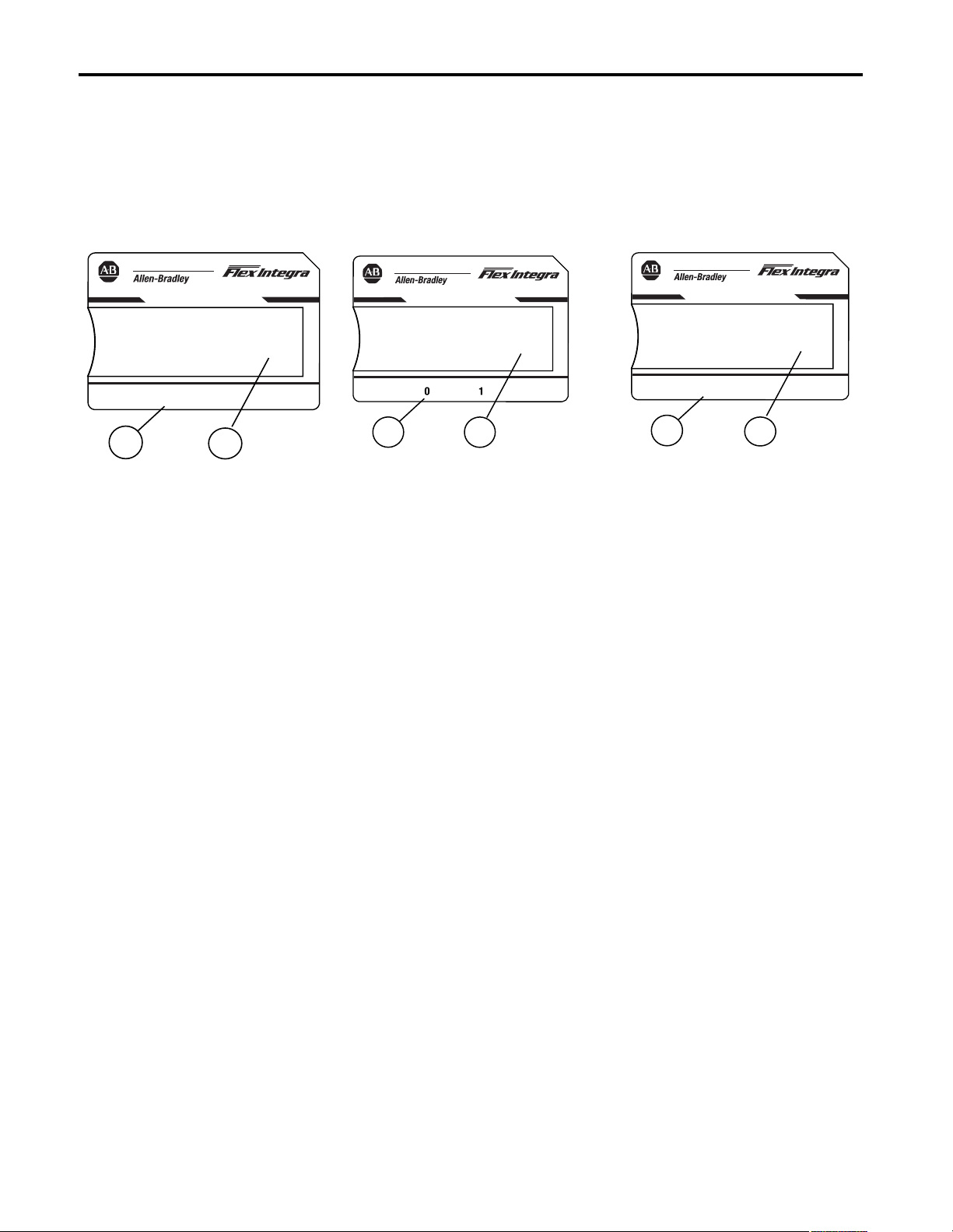
Each module has a unique label identifying its wiring and module type. A
removable label provides space for writing individual designations per
your application.
A
4 INPUT ANALOG
INPUT
0
123
1793-IE4S
B
41350
2 CH ANALOG OUTPUT
A
1793-OE2
41368
B
2 INPUT/1 OUTPUT ANALOG
INPUT
0
1
A
1793-IE2XOE1
OUTPUT
0
B
41491
A = status indicator
B = insertable label
Chapter Summary In this chapter you learned about the FLEX I/O system and the types of
analog modules and how they communicate with programmable
controllers.
Publication 1793-6.5.1 - April 1999
Page 13
Chapter 2
How to Install Your Analog Module
Chapter Objectives
Before You Install Your
Analog Module
In this chapter, we tell you about:
• how to install your module
• how to wire your module
• the indicators
Before installing your analog module in the I/O chassis:
You n e e d to: As described under:
Calculate the power requirements of all
modules in each chassis.
ATTENTION: +24V dc power must be applied to your
module before operation. If power is not applied, the module
position will appear to the adapter as an empty slot in your
chassis. If the adapter does not recognize your module after
installation is completed, cycle power to the adapter.
Power Requirements, page 2-2
Compliance to
European Union Directives
If this product has the CE mark it is approved for installation within the
European Union and EEA regions. It has been designed and tested to meet
the following directives.
EMC Directive
This product is tested to meet Council Directive 89/336/EEC
Electromagnetic Compatibility (EMC) and the following standards, in
whole or in part, documented in a technical construction file:
• EN 50081-2EMC – Generic Emission Standard, Part 2 – Industrial
Environment
• EN 50082-2EMC – Generic Immunity Standard, Part 2 – Industrial
Environment
This product is intended for use in an industrial environment.
Publication 1793-6.5.1 - April 1999
Page 14

2-2 How to Install Your Analog Module
Low Voltage Directive
This product is tested to meet Council Directive 73/23/EEC Low Voltage,
by applying the safety requirements of EN 61131-2 Programmable
Controllers, Part 2 – Equipment Requirements and Tests.
For specific information required by EN 61131-2, see the appropriate
sections in this publication, as well as the following Allen-Bradley
publications:
• Industrial Automation Wiring and Grounding Guidelines For Noise
Immunity, publication 1770-4.1
• Guidelines for Handling Lithium Batteries, publication AG-5.4
• Automation Systems Catalog, publication B111
This equipment is classified as open equipment and must be mounted in an
enclosure during operation to provide safety protection.
Power Requirements
Installing the Module
The wiring of the module is determined by the current draw through the
terminals. Make certain that the current draw does not exceed 10A.
ATTENTION: Total current draw through the module
wiring terminals is limited to 10A. Separate power
connections may be necessary.
ATTENTION: Do not daisy chain power or ground from
an analog module to any ac or dc discrete module.
Installation of the analog module consists of:
This module mounts on a DIN rail. It connects to an adapter or another
FLEX I/O or Integra module. Note: If using this module with FLEX I/O
modules, do not mount between FLEX I/O modules. Mount Integra
modules to the right of the FLEX I/O modules. To mount this module::
1. Remove the cover plug (if used) in the male connector of the unit to
which you are connecting this module.
Publication 1793-6.5.1 - April 1999
Page 15
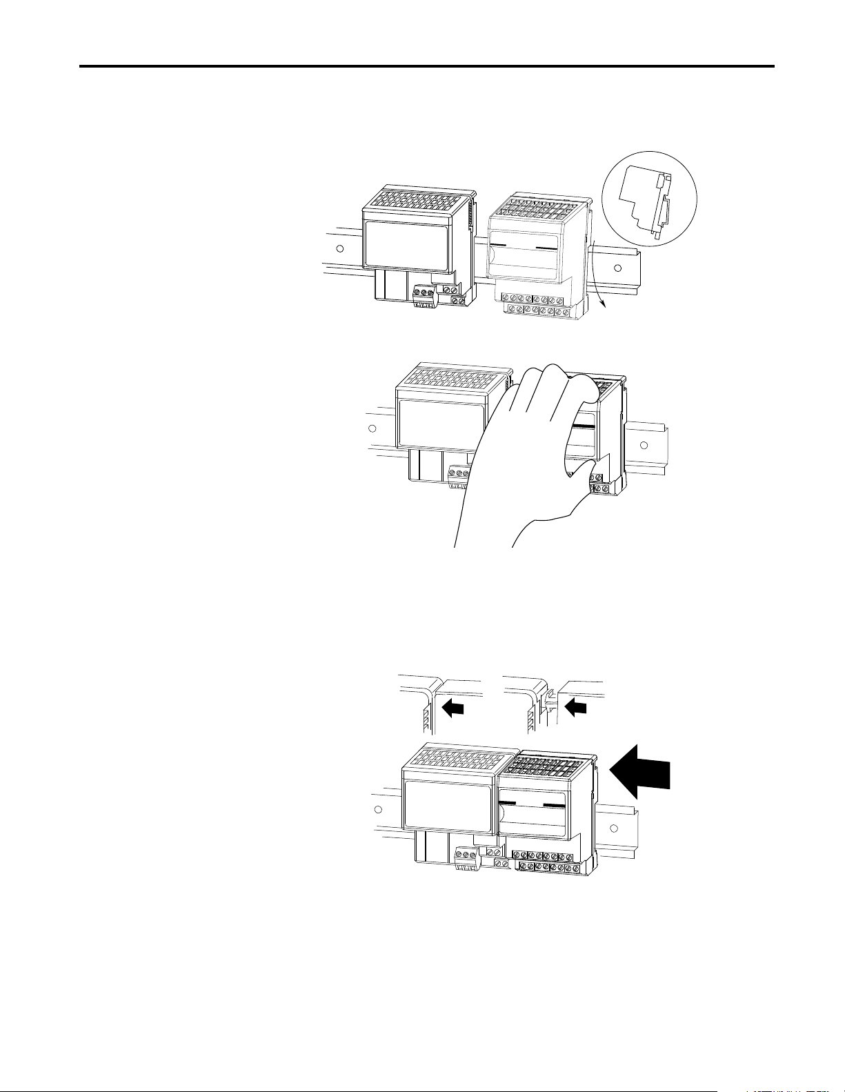
How to Install Your Analog Module 2-3
2. Position the module on the 35 x 7.5mm DIN rail A (A-B pt. no.
199-DR1). Rotate the module onto the DIN rail with the top of the rail
hooked under the lip on the rear of the module.
A
A
30720-M
3. Press down to lock the module on the DIN rail.l
A
41377
If the module does not lock in place, use a screwdriver of similar device
to move the locking tab down, press the module flush with the DIN rail
and release the locking tab to lock the module in place
4. Firmly push the module into the adjacent module/terminal base until the
units lock together.
41371
41370
5. Repeat the above steps to install the next Integra module.
Publication 1793-6.5.1 - April 1999
Page 16
2-4 How to Install Your Analog Module
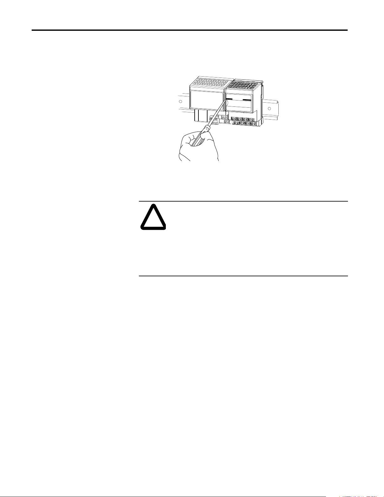
6. To remove an Integra module, you must work from the right side and
remove one module at a time. To disengage a module from its neighbor,
place a common flat-bladed screwdriver between the 2 modules and turn
1/4 turn to separate the modules.
41373
7. Then slide the module away from its left neighbor, and release the
locking lever to remove the module from the DIN rail.
ATTENTION: Do not remove this module under power.
Removing this module under power will break the electrical
backplane (flexbus) connections. This can cause personal injury
or property damage by:
• sending an erroneous signal to your system’s field devices
causing unintended machine motion
• causing an explosion in a hazardous environment
• breaking communication to modules beyond this module
Publication 1793-6.5.1 - April 1999
Page 17
How to Install Your Analog Module 2-5
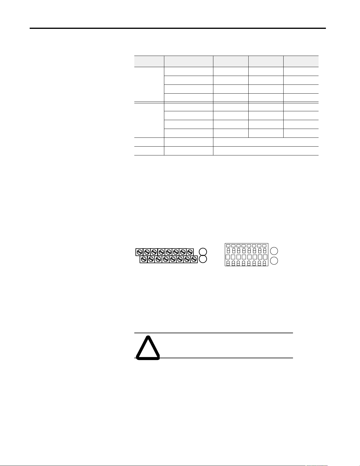
Connecting Wiring for the
Analog Modules
Connecting Wiring for the 1793-IE4 Input Module
This module is available with 2 styles of connectors; screw-cage and spring
clamp. Refer to the wiring figure below.
1793-IE4
Ch 0 Ch 1
CC
01234567
8 9 10 11
CCVV
Ch 2 Ch 3
Where: C = 24V dc common, V = 24V dc power, In = current in, Vn = voltage in
I1I0 V0 V1
I3I2 V2 V3
C
A
B
13 14 1512
41470
C
1. Connect individual analog channel signal wiring to terminals on row A
and row C. Use Belden 8761 cable for signal wiring..
ATTENTION: Connect only 1 current or 1
voltage signal per channel. Do not connect both
current and voltage on 1 channel.
1793-IE4S
Ch 0 Ch 1
CC
V1 V2I2I1
CC
0 1234567
A
B
8 9 10 11 12 13 14 15
VVCC
V3 V4I4I3
Ch 2 Ch 3
41471
2. Connect the associated channel common to common terminals 1, 6, 9 or
14 according to the wiring table on the next page.
3. Connect +24V dc to terminal 8 on row B.
4. Connect 24V dc common to terminal 0 on row A.
5. If daisy-chaining +24V dc from this module to the next FLEX Integra
module, connect a jumper from terminal 15 to terminal 8 on the next
FLEX Integra module.
6. If daisy-chaining 24V dc common from this module to the next FLEX
Integra module, connect a jumper from terminal 7 on this module to
terminal 0 on the next Integra module.
Publication 1793-6.5.1 - April 1999
Page 18
2-6 How to Install Your Analog Module
Table 2.A Wiring connections for the 1793-IE4 Analog Module
Channel Signal Type
0
1
2
3
Current I 2 1
Voltage V 3 1
Current I 4 6
Voltage V 5 3
Current I 10 9
Voltage V 11 9
Current I 12 14
Voltage V 13 14
24V dc Common
+24V dc power
Label
Markings
Signal Return
Terminals 0, 1, 6, 9, and 14 are connected together in
the module.
Terminals 8 and 15 are internally connected in the
module.
Connecting Wiring for the 1793-OE2 Output Module
. This module is available with 2 styles of connectors; 1793-OE2 screw-cage and 1793-OE2S - spring clamp. Refer to the figure below.
1793-OE4 1793-OE4S
Out Ch 0 Out Ch 1
01234567
8 9 10 11
Where: C = common; V = +24V dc power;
I = current output; V = voltage output
I1 V1Io VoCVCCC
13 14 1512
41358
VCC
A
B
Ch0 Ch1
CC
V0I0 V1I1
CC
0 1234567
A
B
8 9 10 11 12 13 14 15
CVVC
41359
1. Connect individual analog output channel signal wiring as follows:
Channel 0 - Current output - connect output signal to terminal 2
(current output) on row A. Connect the associated channel common
to terminal 1 on row A.
Channel 0 - voltage output - connect output signal to terminal 3
(current output) on row A. Connect the associated channel common
to terminal 1 on row A.
Channel 1 - Current output - connect output signal to terminal 4
(current output) on row A. Connect the associated channel common
to terminal 6 on row A.
Channel 0 - voltage output - connect output signal to terminal 5
(current output) on row A. Connect the associated channel common
to terminal 6 on row A.
Publication 1793-6.5.1 - April 1999
1RWH8VH%HOGHQFDEOHIRUVLJQDOZLULQJ
Page 19
How to Install Your Analog Module 2-7
$77(17,21 &RQQHFWRQO\YROWDJHRUFXUUHQWVLJQDO
SHUFKDQQHO'RQRWFRQQHFWERWKYROWDJHDQGFXUUHQWRQRQH
FKDQQHO
2. Connect +24V dc to terminal 8 on row B
3. Connect 24V common to terminal 0 on row A.
4. If daisy-chaining +24V dc from this module to the next FLEX Integra
module, connect a jumper from terminal 15 to terminal 8 on the next
FLEX Integra module.
5. If daisy-chaining 24V dc common from this module to the next FLEX
Integra module, connect a jumper from terminal 7 on this module to
terminal 0 on the next Integra module.
ATTENTION: Total current draw through the
module’s 24V dc terminals is limited to 10A.
Separate power connections to the module may be
required.
$77(17,21'RQRWUHPRYHWKLVPRGXOHXQGHUSRZHU
5HPRYLQJWKLVPRGXOHXQGHUSRZHUZLOOEUHDNWKHHOHFWULFDO
EDFNSODQHIOH[EXVFRQQHFWLRQV7KLVFDQFDXVHSHUVRQDO
LQMXU\RUSURSHUW\GDPDJHE\
VHQGLQJDQHUURQHRXVVLJQDOWR\RXUV\VWHPVILHOG
GHYLFHVFDXVLQJXQLQWHQGHGPDFKLQHPRWLRQ
FDXVLQJDQH[SORVLRQLQDKD]DUGRXVHQYLURQPHQW
EUHDNLQJFRPPXQLFDWLRQWRPRGXOHVEH\RQGWKLV
PRGXOH
ATTENTION: Connect only one current or one voltage
signal per channel. Do not connect both current and voltage
on one channel.
Publication 1793-6.5.1 - April 1999
Page 20
2-8 How to Install Your Analog Module
Tabl e 2.B
Wiring connections for the 1793-OE2 Analog Module
Channel Type Label Marking Signal Return
Current Signal I 2
0
Current Common RET 1
Voltage Signal V 3
Voltage Common RET 1
Current Signal I 4
1
Current Common RET 6
Voltage Signal V 5
Voltage Common RET 6
24V dc Common Terminals 0, 1, 6, 7, 9 and 14
+24V dc Terminals 8 and 15 are internally connected to +V.
Connecting Wiring for the 1793-IE2XOE1 Input/Output Module
This module is available with 2 styles of connectors; screw-cage and spring
clamp. Refer to the wiring figure below.
1793-IE2XOE1
In Ch 1
In Ch 0
CC
01234567
Where: C = common; V = +24V dc power; I
V
= voltage in; Io = current out; Vo = voltage out
0,1
V0 V1I1I0
8 9 10 11
CCVV
Out Ch 0
C
A
B
13 14 1512
VoIo
41473
C
= current in;
0,1
1793-IE2XOE1S
In Ch 1
In Ch 0
CC
V0 V1I1I0
CC
0 1234567
A
B
I
8 9 10 11 12 13 14 15
VVCC
VoIo
Out Ch 0
41472
1. Connect individual analog input channel signal wiring to terminals on
row A. Use terminals 2 (channel 0) and 4 (channel 1) for current and
terminals 3 and 5 for current. Use Belden 8761 cable for signal wiring..
$77(17,21 &RQQHFWRQO\FXUUHQWRUYROWDJHVLJQDO
SHUFKDQQHO'RQRWFRQQHFWERWKFXUUHQWDQGYROWDJHRQ
FKDQQHO
2. Connect the associated channel common to common terminals 1 and 6
according to the wiring table on the next page.
3. Connect individual analog output channel signal wiring to terminals 10
or 11 on row B. (Use terminal 10 for current, or terminal 11 for voltage not both.)
4. Connect the associated channel common to common terminal 9
according to the wiring table on the next page.
Publication 1793-6.5.1 - April 1999
Page 21
How to Install Your Analog Module 2-9
5. Connect +24V dc to terminal 8 on row B
6. Connect 24V dc common to terminal 0 on row A.
7. If daisy-chaining +24V dc from this module to the next FLEX Integra
module, connect a jumper from terminal 15 to terminal 8 on the next
FLEX Integra module.
8. If daisy-chaining 24V dc common from this module to the next FLEX
Integra module, connect a jumper from terminal 7 on this module to
terminal 0 on the next Integra module.
ATTENTION: Total current draw through the terminal
base unit is limited to 10A. Separate power connections to
the terminal base unit may be necessary.
Tabl e 2.C
Wiring connections for the 1794-IE4XOE2 Analog Module
Channel Signal Type
Input
0 Current I 2 1
Voltage V 3
1 Current I 4 6
Voltage V 5
Output
0 Current I 10 9
Voltage V 11
+24V dc Terminals 8 and 15 are internally connected to +V.
24V dc
common
Terminals 0, 1, 6, 7, 9, 14 are internally connected together
in the module.
ATTENTION: Use a 100Ω, 25W or greater,
resistor when connecting to a low-impedence
device, i.e., panel meter. Failure to do so can
result in damage to output circuitry.
Label
Markings
Signal Return
Publication 1793-6.5.1 - April 1999
Page 22
2-10 How to Install Your Analog Module
Module Indicators
4 INPUT ANALOG
iNPUT
0
123
A
The analog modules have status indicators that are on when power is
applied to the module An insertable label is supplied to identify your inputs
and outputs.
1793-IE4S
B
41350
2 CH ANALOG OUTPUT
A
1793-OE2
41368
B
2 INPUT/1 OUTPUT ANALOG
INPUT
0
1
A
1793-IE2XOE1
OUTPUT
0
B
41491
A = status indicator
B = insertable label
Chapter Summary
In this chapter you learned how to install and wire your analog module in an
existing programmable controller system.
Publication 1793-6.5.1 - April 1999
Page 23

Module Programming
Chapter
3
Chapter Objectives
Block Transfer
Programming
In this chapter, we tell you about:
• analog data format
• block transfer programming
• sample programs for the PLC-3 and PLC-5 processors
Your module communicates with the processor through bidirectional block
transfers. This is the sequential operation of both read and write block
transfer instructions.
A configuration block transfer write (BTW) is initiated when the analog
module is first powered up, and subsequently only when the programmer
wants to enable or disable features of the module. The configuration BTW
sets the bits which enable the programmable features of the module, such as
scaling, alarms, ranges, etc. Block transfer reads are performed to retrieve
information from the module.
Block transfer read (BTR) programming moves status and data from the
module to the processor’s data table. The processor user program initiates
the request to transfer data from the module to the processor. The
transferred words contain module status, channel status and input data from
the module.
ATTENTION: If the analog module is not powered up
before the remote I/O adapter, the adapter will not recognize
the module. Make certain that the analog module is installed
and powered before or simultaneously with the remote I/O
adapter. If the adapter does not establish communication with
the module, cycle power to the adapter.
The following sample programs are minimum programs; all rungs and
conditioning must be included in your application program. You can disable
BTRs, or add interlocks to prevent writes if desired. Do not eliminate any
storage bits or interlocks included in the sample programs. If interlocks are
removed, the program may not work properly.
Your program should monitor status bits, block transfer read and block
transfer write activity.
Publication 1793-6.5.1 - April 1999
Page 24

3-2 Module Programming
Sample programs for FLEX
Integra Analog Modules
The following sample programs show you how to use your analog module
efficiently when operating with a programmable controller.
These programs show you how to:
• configure the module
• read data from the module
• update the module’s output channels (if used)
These programs illustrate the minimum programming required for
communication to take place.
PLC-3 Programming
Block transfer instructions with the PLC-3 processor use one binary file in a
data table section for module location and other related data. This is the
block transfer control file. The block transfer data file stores data that you
want transferred to your module (when programming a block transfer write)
or from your module (when programming a block transfer read). The
address of the block transfer data files are stored in the block transfer
control file.
The same block transfer control file is used for both the read and write
instructions for your module. A different block transfer control file is
required for every module.
Program Action
At power-up in RUN mode, or when the
processor is switched from PROG to RUN,
the user program enables a block transfer
read. Then it initiates a block transfer write
to configure the module if the power - up bit
is set.
Thereafter, the program continuously
performs read block transfers.
Note: You must create the data file
for the block transfers before you
enter the block transfer instructions.
The pushbutton allows the user to
manually request a block transfer write to
configure the module.
A sample program segment with block transfer instructions is shown in
Figure 3.1, and described below.
Figure 3.1
PLC-3 Family Sample Program Structure for a 1793-IE4 Module
Block Transfer
Read Done Bit
B3:0
1
15
Block Transfer
Write Done Bit
Pushbutton
2
Power-up Bit
1
Power-up bit included in Series B modules only.
1
B4:8
15
B3:0
05
BTR
BLOCK XFER READ
RACK: 7
GROUP: 0
MODULE: 0
CONTROL: #B3:0
DATA FILE: #B4:0
LENGTH: 9
BTW
BLOCK XFER WRITE
RACK: 7
GROUP: 0
MODULE: 0
CONTROL: #B3:0
DATA FILE: #B5:0
LENGTH: 1
Enable
EN
12
Done
DN
15
Error
ER
13
Enable
EN
02
Done
DN
05
Error
ER
03
Publication 1793-6.5.1 - April 1999
Page 25

Program Action
At power-up in RUN mode, or when the
processor is switched from PROG to RUN,
the user program enables a block transfer
read. Then it initiates a block transfer write
to configure the module and send data
values.
Thereafter, the program continuously
performs read block transfers and write
block transfers.
Note: You must create the data file
for the block transfers before you
enter the block transfer instructions.
Module Programming 3-3
Figure 3.2
PLC-3 Family Sample Program Structure for a 1793-OE2 Module
BTR
Block Transfer
Read Done Bit
1
2
B6:0
15
Block Transfer
Write Done Bit
B6:0
05
BLOCK XFER READ
RACK: 7
GROUP: 1
MODULE: 0
CONTROL: #B6:0
DATA FILE: #B7:0
LENGTH: 1
BTW
BLOCK XFER WRITE
RACK: 7
GROUP: 1
MODULE: 0
CONTROL: #B6:0
DATA FILE: #B8:0
LENGTH: 14
Enable
EN
12
Done
DN
15
Error
ER
13
Enable
EN
02
Done
DN
05
Error
ER
03
Program Action
At power-up in RUN mode, or when the
processor is switched from PROG to RUN,
the user program enables a block transfer
read. Then it initiates a block transfer write
to configure the module and send data values
Thereafter, the program continuously
performs read block transfers and write
block transfers.
Note: You must create the data file
for the block transfers before you
enter the block transfer instructions.
Figure 3.3
PLC-3 Family Sample Program Structure for a 1793-IE2XOE1 Module
BTR
Block Transfer
Read Done Bit
B9:0
1
15
Block Transfer
Write Done Bit
B9:0
2
05
BLOCK XFER READ
RACK: 7
GROUP: 2
MODULE: 0
CONTROL: #B9:0
DATA FILE: #B10:0
LENGTH: 5
BTW
BLOCK XFER READ
RACK: 7
GROUP: 2
MODULE: 0
CONTROL: #B9:0
DATA FILE: #B11:0
LENGTH: 8
Enable
EN
12
Done
DN
15
Error
ER
13
Enable
EN
02
Done
DN
05
Error
ER
03
Publication 1793-6.5.1 - April 1999
Page 26

3-4 Module Programming
Program Action
At power-up in RUN mode, or when the
processor is switched from PROG to RUN,
the user program enables a block transfer
read. Then it initiates a block transfer write
to configure the module if the power-up bit
is set.
Thereafter, the program continuously
performs read block transfers to configure
the module.
The pushbutton allows the user to
manually request a block transfer write.
1
Power-up bit included in Series B modules only.
PLC-5 Programming
The PLC-5 program is very similar to the PLC-3 program with the
following exceptions:
• block transfer enable bits are used instead of done bits as the conditions
on each rung.
• separate block transfer control files are used for the block transfer
instructions.
Figure 3.4
PLC-5 Family Sample Program Structure for the 1793-IE4
N12:0
15
BTR Enable Bit
N12:0
15
BTW Enable Bit
N12:5
15
BTR
BLOCK TRANSFER READ
RACK: 2
GROUP: 1
MODULE: 0
CONTROL: N12:0
DATA FILE: N13:0
LENGTH: 9
CONTINUOUS: N
BTW
BLOCK TRANSFER WRITE
RACK: 2
GROUP: 1
MODULE: 0
CONTROL: N12:5
DATA FILE: N13:20
LENGTH: 1
CONTINUOUS: N
EN
DN
ER
EN
DN
ER
1
2
Pushbutton
Power-up
1
Bit
N13:8
15
BTW Enable Bit
N12:5
15
BTR Enable Bit
Program Action
At power-up in RUN mode, or when the
processor is switched from PROG to RUN,
the user program enables a block transfer
read. Then it initiates a block transfer write
to configure the module and send data values.
Thereafter, the program continuously
performs read block transfers and write block
transfers.
Publication 1793-6.5.1 - April 1999
Figure 3.5
PLC-5 Family Sample Program Structure for the 1793-OE2
BTR Enable Bit
N14:0
1
15
BTW Enable Bit
N14:5
2
15
BTW Enable Bit
N14:5
15
BTR Enable Bit
N14:0
15
BTR
BLOCK TRANSFER READ
RACK: 2
GROUP: 2
MODULE: 0
CONTROL: N14:0
DATA FILE: N15:0
LENGTH: 1
CONTINUOUS: N
BTW
BLOCK TRANSFER WRITE
RACK: 2
GROUP: 2
MODULE: 0
CONTROL: N14:5
DATA FILE: N15:5
LENGTH: 14
CONTINUOUS: N
EN
DN
ER
EN
DN
ER
Page 27

Module Programming 3-5
Figure 3.6
PLC-5 Family Sample Program Structure for the 1793-IE2XOE1
Program Action
At power-up in RUN mode, or when the
processor is switched from PROG to RUN,
the user program enables a block transfer
read. Then it initiates a block transfer write
to configure the module and send data
values.
Thereafter, the program continuously
performs read block transfers and write block
transfers.
BTW Enable Bit
N16:5
1
15
BTR Enable Bit
N16:0
2
15
PLC-2 Programming
BTR Enable Bit
N16:0
15
BTW Enable Bit
N16:5
15
BTR
BLOCK TRANSFER READ
RACK: 2
GROUP: 3
MODULE: 0
CONTROL: N16:0
DATA FILE: N17:0
LENGTH: 5
CONTINUOUS: N
BTW
BLOCK TRANSFER WRITE
RACK: 2
GROUP: 3
MODULE: 0
CONTROL: N16:5
DATA FILE: N17:5
LENGTH: 8
CONTINUOUS: N
EN
DN
ER
EN
DN
ER
Analog Data Format
The 1793 analog I/O modules are not recommended for use with PLC-2
family programmable controllers due to the number of digits needed for
high resolution. In addition, the data returned from the analog-to-digital
converter in the module is 12-bit resolute. This value is left-justified into a
16-bit field, reserving the most significant bit for a sign bit. Refer to
Appendix B for more information.
The data returned from the analog-to-digital converter in the module is
12-bit resolute. This value is left-justified into a 16-bit field, reserving the
most significant bit for a sign bit.
A/D Unipolar Data
Analog Value
Input
A/D Bipolar Data
Analog Value
D/A Data
Output
Analog Value
11 10 09 08 07 06 05 04 03 02 01 00
14 13 12 11 10 09 08 07 06 05 04 03 02 01 00
0*
= Always positive
*
10 09 08 07 06 05 04 03 02 01 00
S
14 13 12 11 10 09 08 07 06 05 04 03 02 01 00
S
11 10 09 08 07 06 05 04 03 02 01 00
S
14 13 12 11 10 09 08 07 06 05 04 03 02 01 00
S
Publication 1793-6.5.1 - April 1999
Page 28

3-6 Module Programming
Refer to Appendix B for a table of values for various current and voltage
modes.
Appendix B also includes an example of scaling.
Chapter Summary
In this chapter, you learned how to program your programmable controller.
You were given sample programs for your PLC-3 and PLC-5 family
processors.
Publication 1793-6.5.1 - April 1999
Page 29

Writing Configuration to and
Reading Status from Your Module
with a Remote I/O Adapter
Chapter
4
Chapter Objectives
Configuring Your Analog
Module
In this chapter, we tell you about:
• configuring your module’s features
• entering your data
• reading data from your module
• read block format
Note: You must use a 1794-ASB series D or later remote I/O adapter to
communicate with the 1793 FLEX Integra analog modules.
Because of the many analog devices available and the wide variety of
possible configurations, you must configure your module to conform to the
analog device and specific application that you have chosen. The module is
configured using a group of data table words that are transferred to the
module using a block transfer write instruction.
The software configurable features available are:
• input/output range selection, including full range and bipolar
• safe state operating value (customer selected analog values the module
will maintain in the event of a network communication error)
Note: PLC-5 family programmable controllers that use 6200 software
programming tools can take advantage of the IOCONFIG utility to
configure these modules. IOCONFIG uses menu-based screens for
configuration without having to set individual bits in particular locations.
Refer to your 6200 software literature for details.
Publication 1793-6.5.1 - April 1999
Page 30

4-2 Writing Configuration to and Reading Status from Your Module with a Remote I/O Adapter
Range Selection
Safe State Value Selection
Individual input channels are configurable to operate with the following
voltage or current ranges:
Bit Settings
Ranges
0-10V dc/0-20mA 0 1
4-20mA 1 0
–10 to +10V dc 1 1
Off 0 0
1
When configured to Off, individual output channels will drive 0V/0mA.
Configure
Select
Full Range
You can select individual channel ranges using the designated words of the
write block transfer instruction. Refer to the Bit/Word description for your
particular module for word and bit numbers.
You can select the analog values that your output module will maintain in
the event of a network communication error. When the multiplex control
bits (M) are cleared simultaneously by a communication error, (or by the
user), the analog outputs will automatically switch to the values set in the
safe state analog words. This allows you to define a safe operating state for
controlled devices which depend on the analog output from the module.
Data Format
Reading Data From Your
Module
Mapping Data for the
Analog Modules
The data returned from the analog-to-digital converter in the module is
12-bit resolute. This value is left-justified into a 16-bit field, reserving the
most significant bit for a sign bit. The 4-20mA mode scales in the module
and uses all 16 bits.
Refer to Appendix C for a table of values for various current and voltage
modes, and an example of scaling to engineering terms.
Read programming moves status and data from the module to the
processor’s data table. The processor’s user program initiates the request to
transfer data from the input module to the processor.
The following read and write words and bit/word descriptions describe the
information written to and read from the analog modules. Each word is
composed of 16 bits.
Publication 1793-6.5.1 - April 1999
Page 31

Writing Configuration to and Reading Status from Your Module with a Remote I/O Adapter 4-3
8 Input Analog Module (Cat. No. 1793-IE4 and -IE4S)
Module Image
Input Data Channel 0
I/O Image
Input Size
1 to 9 Words
PU
Output Size
0 or 1 Word
Analog Input Module (1793-IE4 and -IE4S) Read
Input Data Channel 1
Input Data Channel 2
Input Data Channel 3
Reserved
Reserved
Reserved
Reserved
Underrange
Configure select
Word/Dec. Bit 15 14 13 12 11 10 09 08 07 06 05 04 03 02 01 00
Word/Octal Bit 17 16 15 14 13 12 11 10 07 06 05 04 03 02 01 00
Read Word 0 S Analog Value Channel 0
Word 1 S Analog Value Channel 1
Word 2 S Analog Value Channel 2
Word 3 S Analog Value Channel 3
Word 4 S Reserved
Word 5 S Reserved
Word 6 S Reserved
Word 7 S Reserved
Word 8 PU Not used – set to zero U3 U2 U1 U0
Where: S = sign bit (in 2’s complement)
U = Underrange bits for 4-20mA inputs
PU = Power up bit
Publication 1793-6.5.1 - April 1999
Page 32

4-4 Writing Configuration to and Reading Status from Your Module with a Remote I/O Adapter
Word/Bit Descriptions for the 1793-IE4 and -IE4S Analog Input Module Read
Word
Read Word 0
Word 1
Word 2
Word 3
Words 4-7 Reserved
Word 8
Decimal Bit
(Octal Bit)
Bits 00-14
(00-16)
Bits 15 (17) Channel 0 analog data sign bit.
Bits 00-14
(00-16)
Bits 15 (17) Channel 1 analog data sign bit.
Bits 00-14
(00-16)
Bits 15 (17) Channel 2 analog data sign bit.
Bits 00-14
(00-16)
Bits 15 (17) Channel 3 analog data sign bit.
Bits 00-03
Bits 04-14
(04-16)
Bit 15 (17)
Channel 0 analog data – 12-bit left justified two’s complement number;
unused lower bits are zero; 4-20mA uses all 16 bits.
Channel 1 analog data – 12-bit left justified two’s complement number;
unused lower bits are zero; 4-20mA uses all 16 bits.
Channel 2 analog data – 12-bit left justified two’s complement number;
unused lower bits are zero; 4-20mA uses all 16 bits.
Channel 3 analog data – 12-bit left justified two’s complement number;
unused lower bits are zero; 4-20mA uses all 16 bits.
Underrange bits (U) for individual channels (4-20mA current input only)Bit 00 corresponds to input channel 0, bit 01 corresponds to input channel 1,
and so on. When set (1), indicates either a broken or open input wire, or input
current at or below 4mA.
Not used – set to 0.
Power Up bit .- This bit is set to 1 when all bits in the configuration
register (write word 0) are 0 (unconfigured state). The configuration
register can be cleared by either a reset, or by the user writing all zeroes to it.
Definition
Analog Input Module (1793-IE4 and -IE4S) Write Configuration Block
Word/Dec. Bit 15 14 13 12 11 10 09 08 07 06 05 04 03 02 01 00
Word/Octal Bit 17 16 15 14 13 12 11 10 07 06 05 04 03 02 01 00
Write Word 0 Reserved C3 C2 C1 C0 Reserved F3 F2 F1 F0
Where: C = Configure select bit
F = Full range bit
Publication 1793-6.5.1 - April 1999
Page 33

Writing Configuration to and Reading Status from Your Module with a Remote I/O Adapter 4-5
Range Selection Bits for the 1793-IE4 and -IE4S Analog Input Module
Channel No. Channel 0 Channel 1 Channel 2 Channel 3
F0 C0 F1 C1 F2 C2 F3 C3
Decimal Bits
(Octal Bits)
00
08
(10)
01
09
(11)
02
0-10V dc/0-20mA 1 0 1 0 1 0 1 0
4-20mA 0 1 0 1 0 1 0 1
–10 to +10V dc 1 1 1 1 1 1 1 1
1
Off
C = Configure select bit
F = Full range bit
1
When configured to off, individual channels will return 0000H on Series B modules, and 4
to 20mA on Series A modules.
0 0 0 0 0 0 0 0
Word/Bit Descriptions for the 1793-IE4 and -IE4S Analog Input Module Write
Word Decimal Bit (Octal Bit) Definition
Full range bits (F) for individual channels – Bit 00 corresponds to input channel
0, bit 01 corresponds to input channel 1, and so on.
Configure select bits (C) for individual channels – Bit 08 corresponds to input
channel 0, bit 09 corresponds to input channel 1, and so on. Refer to Range Bit
Write
Word 0
Bits 00-03
Bits 04-07 Reserved
Bits 08-11 (10-13)
Selections.
Bits 12-15 (14-17) Reserved
2 Output Analog Module (Cat. No. 1793-OE2 and -OE2S)
10
(12)
03
11
(13)
Read
Write
I/O Image
Input Size
0 or 1 Word
Output Size
1 to 12 Words
Module Image
PU
Not used Not used
Config. Select Full Range
Not used
Analog Data Channel 0
Analog Data Channel 1
Reserved
Reserved
Not used
Not used
Not used
Not used
Not used
Channel 0 Safe State
Channel 1 Safe State
Diagnostics
M
Publication 1793-6.5.1 - April 1999
Page 34

4-6 Writing Configuration to and Reading Status from Your Module with a Remote I/O Adapter
Analog Output Module (1793-OE2 and -OE2S) Read
Word/Dec. Bit 15 14 13 12 11 10 09 08 07 06 05 04 03 02 01 00
Word/Octal Bit 17 16 15 14 13 12 11 10 07 06 05 04 03 02 01 00
Read Word 0 PU Not used – set to 0 W1 W0
Where: W = Diagnostic bits for current output wire broken or load resistance high. (Not used on voltage outputs.)
PU = Power up bit
Bit/Word Descriptions for the 1793-OE2 and -OE2S Analog Output Module Read
Word
Decimal Bit
(Octal Bit)
Definition
Current outputs only – When set (1), the wire on the output is broken or the
Bits 00-01
load resistance is too high. Bit 00 corresponds to channel 0, bit 01
corresponds to channel 2, and so on.
Read
Word 0
Bits 02-14
(02-16)
Not used – set to 0
Power Up bit. - This bit is set to 1 when all bits in the configuration
Bit 15 (17)
register (write word 5) are 0 (unconfigured state). The configuration
register can be cleared by either a reset, or by the user writing all zeroes to it.
Analog Output Module (1793-OE2 and -OE2S) Write Configuration Block
Word/Dec. Bit 15 14 13 12 11 10 09 08 07 06 05 04 03 02 01 00
Word/Octal Bit 17 16 15 14 13 12 11 10 07 06 05 04 03 02 01 00
Write Word 0 S Analog Data – Channel 0
Word 1 S Analog Data – Channel 1
Word 2 S Reserved
Word 3 S Reserved
Word 4 0 Not used – set to 0 M1 M0
Word 5 0 Not used – set to 0 C1 C0 Not used – set to 0 F1 F0
Word 6 thru 9 Not used – set to 0
Word 10 S Safe State Value – Channel 0
Word 11 S Safe State Value – Channel 1
Word 12 S Reserved
Word 13 S Reserved
Where: S = Sign bit (in 2’s complement)
M = Multiplex control
C = Configure select bit
F = Full range bit
Publication 1793-6.5.1 - April 1999
Page 35

Writing Configuration to and Reading Status from Your Module with a Remote I/O Adapter 4-7
Range Selection Bits for the 1793-OE2 and -OE2S Analog Output Module (Word 5)
Channel No. Channel 0 Channel 1
F0 C0 F1 C1
Decimal Bits (Octal Bits) 00 08 (10) 01 09 (11)
4-20mA 0 1 0 1
0-10V dc/0-20mA 1 0 1 0
–10 to +10V dc 1 1 1 1
1
Off
C = Configure select bit
F = Full range bit
1
When configured to off, individual channels will send 0V or 0mV on
Series B modules. On Series A modules, 2V or 4mA is output until the
module is configured.
0 0 0 0
Word/Bit Descriptions for the 1793-OE2 and -OE2S Analog Output Module Write
Word
Write Word 0
Word 1
Word 2
Word 3
Word 4
Word 5
Words 6 thru 9
Word 10
Word 11
Decimal Bit
(Octal Bit)
Bits 00-14
(00-16)
Channel 0 analog data – 12-bit left justified two’s complement number; unused
lower bits are zero; 4-20mA uses all 16 bits.
Definition
Bits 15 (17) Channel 0 analog data sign bit.
Bits 00-14
(00-16)
Channel 1 analog data – 12-bit left justified two’s complement number; unused
lower bits are zero; 4-20mA uses all 16 bits.
Bits 15 (17) Channel 1 analog data sign bit.
Bits 00-14
(00-16)
Channel 2 analog data – 12-bit left justified two’s complement number; unused
lower bits are zero; 4-20mA uses all 16 bits.
Bits 15 (17) Channel 2 analog data sign bit.
Bits 00-14
(00-16)
Channel 3 analog data – 12-bit left justified two’s complement number; unused
lower bits are zero; 4-20mA uses all 16 bits.
Bits 15 (17) Channel 3 analog data sign bit.
Multiplex control bits (M) for individual channels. These bits control the safe
state analog outputs. – Bit 00 corresponds to output channel 0, bit 01
corresponds to output channel 1, and so on.
Bits 00-03
1 = use words 0 or 1 as directed by channel number n
0 = use words 10 or 11 as directed by channel number n
When bits 00-01 are all cleared (0) simultaneously by a communication error or
user choice thru the programmable controller program, word 5 full range and
configure select bits are preserved at their last setting.
Bits 04-15 (04-17) Not used – set to 0.
Bits 00-01
Full range bits (F) for individual channels – Bit 00 corresponds to output channel
0, and bit 01 corresponds to output channel 1.
Bits 02-07 Not used – set to 0.
Bits 08-09 (10-11)
Configure select bits (C) for individual channels – Bit 08 corresponds to output
channel 0, and bit 09 corresponds to output channel 1.
Bits 10-15 (12-17) Not used – set to 0.
Bits 00-15
(00-17)
Bits 00-14
(00-16)
Not used – set to 0.
Channel 0 Safe State analog value – 12-bit left justified two’s complement
number; unused lower bits are zero; 4-20mA uses all 16 bits.
Bits 15 (17) Channel 0 Safe State analog data sign bit.
Bits 00-14
(00-16)
Channel 1 Safe State analog value – 12-bit left justified two’s complement
number; unused lower bits are zero; 4-20mA uses all 16 bits.
Bits 15 (17) Channel 1 Safe State analog data sign bit.
Publication 1793-6.5.1 - April 1999
Page 36

4-8 Writing Configuration to and Reading Status from Your Module with a Remote I/O Adapter
Word
Words 12-13
Decimal Bit
(Octal Bit)
Bits 00-15
(00-17)
Definition
Reserved
2 Input/1 Output Analog Combo Module (Cat. No. 1793-IE2XOE1 and -IE2XOE1S)
Module Image
Read
Write
I/O Image
Input Size
0 to 5 Words
Output Size
0 to 7 Words
PU
Not used Full Range and Configure Select
Input Data Channel 0
Input Data Channel 1
Reserved
Reserved
Underrange & Diag.
Output Data Channel 0
Reserved
Not used
Not used
Not used
Output Channel 0 Safe State
M
Analog Combo Module (1793-IE4XOE1) Read
Word/Dec. Bit 15 14 13 12 11 10 09 08 07 06 05 04 03 02 01 00
Word/Octal Bit 17 16 15 14 13 12 11 10 07 06 05 04 03 02 01 00
Read Word 0 S Analog Value Input Channel 0
Word 1 S Analog Value Input Channel 1
Word 2 S
Word 3 S
Word 4 PU Not used – set to 0 W1 W0
Where: S = sign bit (in 2’s complement)
W = Diagnostic bits for current output wire broken or load resistance high. (Not used on voltage outputs.)
PU = Power up bit
Word/Bit Descriptions for the 1794-IE4XOE1 and -IE2XOE1S Analog Combo
Module Read
Word
Read
Word 0
Word 1
Words 2
and 3
Decimal Bit
(Octal Bit)
Bits 00-14
(00-16)
Channel 0 analog data – 12-bit left justified two’s complement number;
unused lower bits are zero; 4-20mA uses all 16 bits.
Bits 15 (17) Channel 0 analog data sign bit.
Bits 00-14
(00-16)
Channel 1 analog data – 12-bit left justified two’s complement number;
unused lower bits are zero; 4-20mA uses all 16 bits.
Bits 15 (17) Channel 1 analog data sign bit.
Reserved
Definition
Publication 1793-6.5.1 - April 1999
Page 37

Writing Configuration to and Reading Status from Your Module with a Remote I/O Adapter 4-9
Word
Word 4
Decimal Bit
(Octal Bit)
Bits 00-01
Definition
Underrange bits (U) for individual channels (4-20mA current input only)-
Bit 00 corresponds to input channel 0, bit 01 corresponds to input channel 1.
When set (1), indicates either a broken or open input wire, or input current at
or below 4mA.
Bits 02-03 Reserved
Wire Off bits (W) – Current outputs only – When set (1), the wire on the
Bits 04
current output is broken or the load resistance is too high. Bit 00 corresponds
to channel 0.
Bits 05-14
(05-16)
Reserved
Power Up bit - This bit is set to 1 when all bits in the configuration
Bit 15 (17)
register (write word 3) are 0 (unconfigured state). The configuration
register can be cleared by either a reset, or by the user writing all zeroes to it.
Analog Combo Module (1793-IE2XOE1 and -IE2XOE1S) Write Configuration Block
Word/Dec. Bit 15 14 13 12 11 10 09 08 07 06 05 04 03 02 01 00
Word/Octal Bit 17 16 15 14 13 12 11 10 07 06 05 04 03 02 01 00
Write Word 0 S Analog Data – Output Channel 0
Word 1 S Reserved
Word 2 0 Not used – set to 0 M0
Word 3 Not used C5 C4 C3 C2 C1 C0 0 0 0 F4 0 0 F1 F0
Words 4 and 5 Not used – set to 0
Word 6 S Safe State Value – Output Channel 0
Word 7 S Reserved
Where: M = Multiplex control bits
S = Sign bit (in 2’s complement)
C = Configure select bit
F = Full range bit
Publication 1793-6.5.1 - April 1999
Page 38

4-10 Writing Configuration to and Reading Status from Your Module with a Remote I/O Adapter
Range Selection Bits for the 1793-IE2XOE1 and -IE2XOE1S Analog Combo Module
Channel No.
Decimal Bits
(Octal Bits)
0-10V dc/0-20mA 1 0 1 0 1 0
–10 to +10V dc 1 1 1 1 1 1
C = Configure select bit
F = Full range bit
1
When configured to off, individual channels will return 0000H.
Word/Bit Descriptions for the 1793-IE2XOE1 and -IE2XOE1S Analog Combo
Module Write
Word
Write
Word 0
Word 1 Bits 00-15
Word 2
Word 3
Decimal Bit
(Octal Bit)
Bits 00-14
(00-16)
Bits 15
(17)
(00-17
Bit 00
Bits 01-15 (01-17) Not used – set to 0.
Bits 00-01, 04
Bits 02, 03, 05-07 Not used – set to 0.
Bits 08-09, 12 (10,
11, 13-15)
Bits 14-15 (16-17) Not used – set to 0.
Input
Channel 0
Input
Channel 1
Output
Channel 0
F0 C0 F1 C1 F4 C4
00
08
(10)
01
09
(11)
04
12
(14)
4-20mA 0 1 0 1 0 1
Off
1
0 0 0 0 0 0
Definition
Channel 0 analog data – 12-bit left justified two’s complement number; unused
lower bits are zero; 4-20mA uses all 16 bits.
Channel 0 analog data sign bit.
Reserved
Multiplex control bits (M) for individual channel. This bit controls the safe state
analog outputs– Bit 00 corresponds to output channel 0.
1 = use words 0 (analog value) as directed by channel number n
0 = use words 6 (safe state analog value) as directed by channel number n
When bit 00 is cleared (0) simultaneously by a communication error or user choice
thru the programmable controller program, word 3 full range and configure select
bits are preserved at their last setting.
Full range bits (F) for individual channels – Bit 00 corresponds to input channel 0,
bit 01 corresponds to input channel 1, and bit 04 corresponds to output channel 1.
Refer to Range Bit Selections.
Configure select bits (C) for individual channels – Bit 08 corresponds to input
channel 0, bit 09 (11) corresponds to input channel 1, bit 12 (14) corresponds to
output channel 0. Refer to Range Bit Selections.
Publication 1793-6.5.1 - April 1999
Page 39

Writing Configuration to and Reading Status from Your Module with a Remote I/O Adapter 4-11
Chapter Summary
Word
Words 4
and 5
Word 6
Word 7
Decimal Bit
(Octal Bit)
Not used – set to 0.
Bits 00-14
(00-16)
Bits 15 (17) Channel 0 Safe State analog data sign bit.
Bits 00-14
(00-16)
Bits 15 (17) Channel 1 Safe State analog data sign bit.
Channel 0 Safe State analog value – 12-bit left justified two’s complement number;
unused lower bits are zero; 4-20mA uses all 16 bits.
Channel 1 Safe State analog value – 12-bit left justified two’s complement number;
unused lower bits are zero; 4-20mA uses all 16 bits.
Definition
In this chapter you learned how to configure your module’s features and
enter your data.
Publication 1793-6.5.1 - April 1999
Page 40

How Communication Takes Place
and I/O Image Table Mapping
with the DeviceNet Adapter
Chapter
5
Chapter Objectives
About DeviceNetManager
Software
Polled I/O Structure
In this chapter, we tell you about:
• DeviceNetManager software
• I/O structure
• image table mapping
• factory defaults
DeviceNetManager software is a tool used to configure your FLEX I/O
DeviceNet adapter and its related modules, including any FLEX Integra
modules. This software tool can be connected to the adapter via the
DeviceNet network.
You must understand how DeviceNetManager software works in order to
add a device to the network. Refer to the DeviceNetManager Software User
Manual, publication 1787-6.5.3.
Output data is received by the adapter in the order of the installed I/O
modules. The Output data for Slot 0 is received first, followed by the
Output data for Slot 1, and so on up to slot 7.
The first word of input data sent by the adapter is the Adapter Status Word.
This is followed by the input data from each slot, in the order of the
installed I/O modules. The Input data from Slot 0 is first after the status
word, followed by Input data from Slot 2, and so on up to slot 7.
Network READ
Network WRITE
DeviceNet Adapter
Read Data
Adapter Status
Slot 0 Input Data
Slot 1 Input Data
...
...
Slot 7 Input Data
Write Data
Slot 0 Output Data
Slot 1 Output Data
...
...
Slot 7 Output Data
Read
Write
I/O Module
Slot 0
I/O Module
Publication 1793-6.5.1 - April 1999
Slot 1
...
I/O Module
Slot 7
Page 41

5-2 How Communication Takes Place and I/O Image Table Mapping with the DeviceNet Adapter
Adapter Input Status Word
The input status word consists of:
• I/O module fault bits – 1 status bit for each slot
• node address changed – 1 bit
• I/O status – 1 bit
10 through 15
15Bit: 012345678
9
I/O Module Fault Bits
Not Used
I/O State Bit
Node Address Changed Bit
Slot 7
Slot 6
Slot 5
Slot 4
Slot 3
Slot 2
Slot 1
Slot 0
The adapter input status word bit descriptions are shown in the following
table.
Bit Description Bit Explanation
0 This bit is set (1) when an error is detected in slot position 0.
1 This bit is set (1) when an error is detected in slot position 1.
2 This bit is set (1) when an error is detected in slot position 2.
I/O Module Fault
Node Address Changed 8
I/O State 9
3 This bit is set (1) when an error is detected in slot position 3.
4 This bit is set (1) when an error is detected in slot position 4.
5 This bit is set (1) when an error is detected in slot position 5.
6 This bit is set (1) when an error is detected in slot position 6.
7 This bit is set (1) when an error is detected in slot position 7.
This bit is set (1) when the node address switch setting has been
changed since power up.
Bit = 0 – idle
Bit = 1 – run
10 thru 15 Not used – sent as zeroes.
Publication 1793-6.5.1 - April 1999
Possible causes for an I/O Module Fault are:
• transmission errors on the Flex I/O backplane
• a failed module
• a module removed from its terminal base
• incorrect module inserted in a slot position
• the slot is empty
The node address changed bit is set when the node address switch setting
has been changed since power up. The new node address does not take
affect until the adapter has been powered down and then powered back up.
Page 42

How Communication Takes Place and I/O Image Table Mapping with the DeviceNet Adapter 5-3
System Throughput
Mapping Data into the
Image Table
System throughput, from analog input to backplane, is a function of:
• the data format selected
• the type and mode of sensors selected
• whether filtering is selected
The A/D converter which converts channel 0 through 7 analog data to a
digital word provides a programmable single low pass filter. You can set the
frequency of this filter during module configuration. The selection
influences the A/D output data rate, thus affecting system throughput.
FLEX Integra analog input module data table mapping is shown below.
4 Input Analog Module (Cat. No. 1793-IE4 and -IE4S)
Module Image
Input Data Channel 0
I/O Image
Input Size
1 to 9 Words
PU
Output Size
0 or 6 Words
Input Data Channel 1
Input Data Channel 2
Input Data Channel 3
Reserved
Reserved
Reserved
Reserved
Underrange
Configure select
Reserved
Reserved
Reserved
Reserved
Reserved
Publication 1793-6.5.1 - April 1999
Page 43

5-4 How Communication Takes Place and I/O Image Table Mapping with the DeviceNet Adapter
Analog Input Module (1793-IE4 and -IE4S) Read
Word/Dec. Bit 15 14 13 12 11 10 09 08 07 06 05 04 03 02 01 00
Word/Octal Bit 17 16 15 14 13 12 11 10 07 06 05 04 03 02 01 00
Read Word 1 S Analog Value Channel 0
Word 2 S Analog Value Channel 1
Word 3 S Analog Value Channel 2
Word 4 S Analog Value Channel 3
Word 5 S Reserved
Word 6 S Reserved
Word 7 S Reserved
Word 8 S Reserved
Word 9 PU Not used – set to zero U3 U2 U1 U0
Where: S = sign bit (in 2’s complement)
U = Underrange bits for 4-20mA inputs
PU = Power up bit
Word/Bit Descriptions for the 1793-IE4 and -IE4S Analog Input Module Read
Word
Read Word 1
Word 2
Word 3
Word 4
Words 5-8 Reserved
Word 9
Decimal Bit
(Octal Bit)
Bits 00-14
(00-16)
Bits 15 (17) Channel 0 analog data sign bit.
Bits 00-14
(00-16)
Bits 15 (17) Channel 1 analog data sign bit.
Bits 00-14
(00-16)
Bits 15 (17) Channel 2 analog data sign bit.
Bits 00-14
(00-16)
Bits 15 (17) Channel 3 analog data sign bit.
Bits 00-03
Bits 04-14
(04-16)
Bit 15 (17)
Channel 0 analog data – 12-bit left justified two’s complement number;
unused lower bits are zero; 4-20mA uses all 16 bits.
Channel 1 analog data – 12-bit left justified two’s complement number;
unused lower bits are zero; 4-20mA uses all 16 bits.
Channel 2 analog data – 12-bit left justified two’s complement number;
unused lower bits are zero; 4-20mA uses all 16 bits.
Channel 3 analog data – 12-bit left justified two’s complement number;
unused lower bits are zero; 4-20mA uses all 16 bits.
Underrange bits (U) for individual channels (4-20mA current input only)Bit 00 corresponds to input channel 0, bit 01 corresponds to input channel 1,
and so on. When set (1), indicates either a broken or open input wire, or input
current at or below 4mA.
Not used – set to 0.
Power Up bit .- This bit is set to 1 when all bits in the configuration
register (write word 0) are 0 (unconfigured state). The configuration
register can be cleared by either a reset, or by the user writing all zeroes to it.
Definition
Word/Dec. Bit 15 14 13 12 11 10 09 08 07 06 05 04 03 02 01 00
Word/Octal Bit 17 16 15 14 13 12 11 10 07 06 05 04 03 02 01 00
Write Word 1 Reserved C3 C2 C1 C0 Reserved F3 F2 F1 F0
Where: C = Configure select bit
Publication 1793-6.5.1 - April 1999
Analog Input Module (1793-IE4 and -IE4S) Write Configuration Block
2 Reserved
3 Reserved
4 Reserved
5 Reserved
6 Reserved
F = Full range bit
Page 44

How Communication Takes Place and I/O Image Table Mapping with the DeviceNet Adapter 5-5
Range Selection Bits for the 1793-IE4 and -IE4S Analog Input Module
Channel No. Channel 0 Channel 1 Channel 2 Channel 3
F0 C0 F1 C1 F2 C2 F3 C3
Decimal Bits
(Octal Bits)
00
08
(10)
01
09
(11)
02
0-10V dc/0-20mA 1 0 1 0 1 0 1 0
4-20mA 0 1 0 1 0 1 0 1
–10 to +10V dc 1 1 1 1 1 1 1 1
1
Off
C = Configure select bit
F = Full range bit
1
When configured to off, individual channels will return 0000H on Series B modules, and 4
to 20mA on Series A modules.
0 0 0 0 0 0 0 0
Word/Bit Descriptions for the 1793-IE4 and -IE4S Analog Input Module Write
Word Decimal Bit (Octal Bit) Definition
Bits 00-03
Write
Word 1
Bits 04-07 Reserved
Bits 08-11 (10-13)
Bits 12-15 (14-17) Reserved
2 Bits 01-15 (01-17) Reserved
3 Bits 01-15 (01-17) Reserved
4 Bits 01-15 (01-17) Reserved
5 Bits 01-15 (01-17) Reserved
6 Bits 01-15 (01-17) Reserved
Full range bits (F) for individual channels – Bit 00 corresponds to input channel
0, bit 01 corresponds to input channel 1, and so on.
Configure select bits (C) for individual channels – Bit 08 corresponds to input
channel 0, bit 09 corresponds to input channel 1, and so on. Refer to Range Bit
Selections.
10
(12)
03
11
(13)
Publication 1793-6.5.1 - April 1999
Page 45

5-6 How Communication Takes Place and I/O Image Table Mapping with the DeviceNet Adapter
2 Output Analog Module (Cat. No. 1793-OE2 and -OE2S)
Read
Write
I/O Image
Input Size
0 or 1 Word
PU
Module Image
Not used
Analog Data Channel 0
Analog Data Channel 1
Reserved
Reserved
Not used
Output Size
1 to 14 Words
Not used Not used
Config. Select
Not used
Not used
Not used
Not used
Not used
Not used
Not used
Not used
Analog Output Module (1793-OE2 and -OE2S) Read
Diagnostics
M
Full Range
Word/Dec. Bit 15 14 13 12 11 10 09 08 07 06 05 04 03 02 01 00
Word/Octal Bit 17 16 15 14 13 12 11 10 07 06 05 04 03 02 01 00
Read Word 1 PU Not used – set to 0 W1 W0
Where: W = Diagnostic bits for current output wire broken or load resistance high. (Not used on voltage outputs.)
PU = Power up bit
Bit/Word Descriptions for the 1793-OE2 and -OE2S Analog Output Module Read
Word
Read
Word 1
Decimal Bit
(Octal Bit)
Bits 00-01
Bits 02-14
(02-16)
Bit 15 (17)
Definition
Current outputs only – When set (1), the wire on the output is broken or the
load resistance is too high. Bit 00 corresponds to channel 0, bit 01
corresponds to channel 2, and so on.
Not used – set to 0
Power Up bit. - This bit is set to 1 when all bits in the configuration
register (write word 5) are 0 (unconfigured state). The configuration
register can be cleared by either a reset, or by the user writing all zeroes to it.
Publication 1793-6.5.1 - April 1999
Page 46

How Communication Takes Place and I/O Image Table Mapping with the DeviceNet Adapter 5-7
Analog Output Module (1793-OE2 and -OE2S) Write Configuration Block
Word/Dec. Bit 15 14 13 12 11 10 09 08 07 06 05 04 03 02 01 00
Word/Octal Bit 17 16 15 14 13 12 11 10 07 06 05 04 03 02 01 00
Write Word 1 S Analog Data – Channel 0
Word 2 S Analog Data – Channel 1
Word 3 S Reserved
Word 4 S Reserved
Word 5 0 Not used – set to 0 M1 M0
Word 6 0 Not used – set to 0 C1 C0 Not used – set to 0 F1 F0
Word 7 thru 10 Not used – set to 0
Word 11 S Reserved
Word 12 S Reserved
Word 13 S Reserved
Word 14 S Reserved
Where: S = Sign bit (in 2’s complement)
M = Multiplex control
C = Configure select bit
F = Full range bit
Range Selection Bits for the 1793-OE2 and -OE2S Analog Output Module (Word 5)
Channel No. Channel 0 Channel 1
F0 C0 F1 C1
Decimal Bits (Octal Bits) 00 08 (10) 01 09 (11)
4-20mA 0 1 0 1
0-10V dc/0-20mA 1 0 1 0
–10 to +10V dc 1 1 1 1
1
Off
C = Configure select bit
F = Full range bit
1
When configured to off, individual channels will send 0V or 0mV on
Series B modules. On Series A modules, 2V or 4mA is output until the
module is configured.
0 0 0 0
Publication 1793-6.5.1 - April 1999
Page 47

5-8 How Communication Takes Place and I/O Image Table Mapping with the DeviceNet Adapter
Word/Bit Descriptions for the 1793-OE2 and -OE2S Analog Output Module Write
Word
Write Word 1
Word 2
Word 3
Word 4
Word 5
Word 6
Words 7 thru
10
Words 11-14
Decimal Bit
(Octal Bit)
Bits 00-14
(00-16)
Bits 15 (17) Channel 0 analog data sign bit.
Bits 00-14
(00-16)
Bits 15 (17) Channel 1 analog data sign bit.
Bits 00-14
(00-16)
Bits 15 (17) Channel 2 analog data sign bit.
Bits 00-14
(00-16)
Bits 15 (17) Channel 3 analog data sign bit.
Bits 00-03
Bits 04-15 (04-17) Not used – set to 0.
Bits 00-01
Bits 02-07 Not used – set to 0.
Bits 08-09 (10-11)
Bits 10-15 (12-17) Not used – set to 0.
Bits 00-15
(00-17)
Bits 00-15
(00-17)
Channel 0 analog data – 12-bit left justified two’s complement number; unused
lower bits are zero; 4-20mA uses all 16 bits.
Channel 1 analog data – 12-bit left justified two’s complement number; unused
lower bits are zero; 4-20mA uses all 16 bits.
Channel 2 analog data – 12-bit left justified two’s complement number; unused
lower bits are zero; 4-20mA uses all 16 bits.
Channel 3 analog data – 12-bit left justified two’s complement number; unused
lower bits are zero; 4-20mA uses all 16 bits.
Multiplex control bits (M) for individual channels. These bits control the safe
state analog outputs. – Bit 00 corresponds to output channel 0, bit 01
corresponds to output channel 1, and so on.
1 = use words 0 or 1 as directed by channel number n
0 = use words 10 or 11 as directed by channel number n
When bits 00-01 are all cleared (0) simultaneously by a communication error or
user choice thru the programmable controller program, word 6 full range and
configure select bits are preserved at their last setting.
Full range bits (F) for individual channels – Bit 00 corresponds to output channel
0, and bit 01 corresponds to output channel 1.
Configure select bits (C) for individual channels – Bit 08 corresponds to output
channel 0, and bit 09 corresponds to output channel 1.
Not used – set to 0.
Reserved
Definition
Publication 1793-6.5.1 - April 1999
Page 48

How Communication Takes Place and I/O Image Table Mapping with the DeviceNet Adapter 5-9
odu e age
2 Input/1 Output Analog Combo Module (Cat. No. 1793-IE2XOE1 and -IE2XOE1S)
Read
Write
I/O Image
Input Size
0 to 5 Words
Output Size
0 to 10 Words
PU
Not used Full Range and Configure Select
Input Data Channel 0
Input Data Channel 1
Reserved
Reserved
Underrange & Diag.
Output Data Channel 0
Reserved
Not used
Not used
Not used
Reserved
Reserved
Reserved
Reserved
M
Analog Combo Module (1793-IE2XOE1 and -IE2XOE1S) Read
Word/Dec. Bit 15 14 13 12 11 10 09 08 07 06 05 04 03 02 01 00
Word/Octal Bit 17 16 15 14 13 12 11 10 07 06 05 04 03 02 01 00
Read Word 1 S Analog Value Input Channel 0
Word 2 S Analog Value Input Channel 1
Word 3 S Reserved
Word 4 S Reserved
Word 5 PU Not used – set to 0 W1 W0
Where: S = sign bit (in 2’s complement)
W = Diagnostic bits for current output wire broken or load resistance high. (Not used on voltage outputs.)
PU = Power up bit
Word/Bit Descriptions for the 1793-IE2XOE1 and -IE2XOE1S Analog Combo
Module Read
Word
Read
Word 1
Word 2
Words 3
and 4
Decimal Bit
(Octal Bit)
Bits 00-14
(00-16)
Channel 0 analog data – 12-bit left justified two’s complement number;
unused lower bits are zero; 4-20mA uses all 16 bits.
Bits 15 (17) Channel 0 analog data sign bit.
Bits 00-14
(00-16)
Channel 1 analog data – 12-bit left justified two’s complement number;
unused lower bits are zero; 4-20mA uses all 16 bits.
Bits 15 (17) Channel 1 analog data sign bit.
Reserved
Definition
Publication 1793-6.5.1 - April 1999
Page 49

5-10 How Communication Takes Place and I/O Image Table Mapping with the DeviceNet Adapter
Word
Word 5
Decimal Bit
(Octal Bit)
Bits 00-01
Definition
Underrange bits (U) for individual channels (4-20mA current input only)-
Bit 00 corresponds to input channel 0, bit 01 corresponds to input channel 1.
When set (1), indicates either a broken or open input wire, or input current at
or below 4mA.
Bits 02-03 Reserved
Wire Off bits (W) – Current outputs only – When set (1), the wire on the
Bits 04
current output is broken or the load resistance is too high. Bit 00 corresponds
to channel 0.
Bits 05-14
(05-16)
Reserved
Power Up bit - This bit is set to 1 when all bits in the configuration
Bit 15 (17)
register (write word 3) are 0 (unconfigured state). The configuration
register can be cleared by either a reset, or by the user writing all zeroes to it.
Analog Combo Module (1793-IE2XOE1 and -IE2XOE1S) Write Configuration Block
Word/Dec. Bit 15 14 13 12 11 10 09 08 07 06 05 04 03 02 01 00
Word/Octal Bit 17 16 15 14 13 12 11 10 07 06 05 04 03 02 01 00
Write Word 1 S Analog Data – Output Channel 0
Word 2 S Reserved
Word 3 0 Not used – set to 0 M0
Word 4 Not used C5 C4 C3 C2 C1 C0 0 0 0 F4 0 0 F1 F0
Words 5 and 6 Not used – set to 0
Word 7 Reserved
Word 8 Reserved
Word 9 Reserved
Word 10 Reserved
Where: M = Multiplex control bits
S = Sign bit (in 2’s complement)
C = Configure select bit
F = Full range bit
Publication 1793-6.5.1 - April 1999
Range Selection Bits for the 1793-IE2XOE1 and -IE2XOE1S Analog Combo Module
Channel No.
Input
Channel 0
F0 C0 F1 C1 F4 C4
Decimal Bits
(Octal Bits)
00
08
(10)
4-20mA 0 1 0 1 0 1
0-10V dc/0-20mA 1 0 1 0 1 0
–10 to +10V dc 1 1 1 1 1 1
1
Off
C = Configure select bit
F = Full range bit
1
When configured to off, individual channels will return 0000H.
0 0 0 0 0 0
Input
Channel 1
09
01
(11)
Output
Channel 0
12
04
(14)
Page 50

How Communication Takes Place and I/O Image Table Mapping with the DeviceNet Adapter 5-11
Word/Bit Descriptions for the 1793-IE2XOE1 and -IE2XOE1S Analog Combo
Module Write
Word
Write
Word 1
Word 2 Bits 00-15
Word 3
Word 4
Words 5
and 6
Words 7
thru 10
Decimal Bit
(Octal Bit)
Bits 00-14
(00-16)
Bits 15
(17)
(00-17
Bit 00
Bits 01-15 (01-17) Not used – set to 0.
Bits 00-01, 04
Bits 02, 03, 05-07 Not used – set to 0.
Bits 08-09, 12 (10,
11, 13-15)
Bits 14-15 (16-17) Not used – set to 0.
Bits 01-15 (01-17) Not used – set to 0.
Bits 01-15 (01-17) Reserved
Definition
Channel 0 analog data – 12-bit left justified two’s complement number; unused
lower bits are zero; 4-20mA uses all 16 bits.
Channel 0 analog data sign bit.
Reserved
Multiplex control bits (M) for individual channel. This bit controls the safe state
analog outputs– Bit 00 corresponds to output channel 0.
1 = use words 0 (analog value) as directed by channel number n
0 = use words 6 (safe state analog value) as directed by channel number n
When bit 00 is cleared (0) simultaneously by a communication error or user choice
thru the programmable controller program, word 4 full range and configure select
bits are preserved at their last setting.
Full range bits (F) for individual channels – Bit 00 corresponds to input channel 0,
bit 01 corresponds to input channel 1, and bit 04 corresponds to output channel 1.
Refer to Range Bit Selections.
Configure select bits (C) for individual channels – Bit 08 corresponds to input
channel 0, bit 09 (11) corresponds to input channel 1, bit 12 (14) corresponds to
output channel 0. Refer to Range Bit Selections.
Defaults
Each I/O module has default values associated with it. At default, each
module will generate inputs/status and expect outputs/configuration.
Module Defaults for: Factory Defaults Real Time Size
Catalog
Number
1793-IE4 4-Input Module 11 4 8 0
1793-OE2 2-Output Module 11 4 8 0
1793-IE2XOE1 2-Input/1 Output Module 11 4 8 0
Description
Input
Default
Output
Default
Input
Default
Output
Default
Factory defaults are the values assigned by the adapter when you:
• first power up the system, and
• no previous stored settings have been applied.
For analog modules, the defaults reflect the actual number of input words/
output words. For example, for the 4-input module, you have 11 input
words, and 4 output words.
Publication 1793-6.5.1 - April 1999
Page 51

5-12 How Communication Takes Place and I/O Image Table Mapping with the DeviceNet Adapter
You can change the I/O data size for a module by reducing the number of
words mapped into the adapter module, as shown in “real time sizes.”
Real time sizes are the settings that provide optimal real time data to the
adapter module.
Analog modules have 15 words assigned to them. This is divided into input
words/output words. You can reduce the I/O data size to fewer words to
increase data transfer over the backplane.
For information on using DeviceNetManager software to configure your
adapter, refer to the DeviceNetManager Software User Manual, publication
1787-6.5.3.
Chapter Summary
In this chapter, you learned how this module communicates over the
DeviceNet network, and the image table mapping for the module.
Publication 1793-6.5.1 - April 1999
Page 52

Chapter
6
Input, Status, Output and Configuration Files
using ControlNet
What this Chapter Contains
About the ControlNet Adapter
Communication Over the
FLEX I/O Backplane
Read this chapter to familiarize yourself with input, output and
configuration files for analog I/O modules on ControlNet.This chapter talks
about:
• the ControlNet Adapter
• I/O structure
• fault state data
• communication fault data
• idle state behavior
• input data behavior upon module removal
The FLEX I/O ControlNet adapter (cat. no. 1794-ACN15 or -ACNR15)
interfaces up to 8 FLEX I/O and/or FLEX Integra modules and a
ControlNet processor or scanner. The adapter can support ControlNet
real-time data connections to individual modules or module groups. Each
connection is independent of the others and can be from different processors
or scanners.
One ControlNet adapter can interface up to eight terminal base units with
installed FLEX I/O and/or FLEX Integra modules, forming a
FLEX I/O system of up to eight slots. The adapter communicates to other
network system components (typically one or more controllers or scanners,
and/or programming terminals) over the ControlNet network. The adapter
communicates with its I/O modules over the flexbus backplane.
Network
ControlNet
Adapter
Write
Read
I/O Module I/O ModuleI/O Module
Inputs Inputs Inputs
Status
Outputs
Configuration Configuration Configuration
Slot 0 Slot 1 Slot 7
0
Read
Words
Write
Words
X
Publication 1793-6.5.1 - April 1999
StatusStatus
OutputsOutputs
41626
Page 53

6-2 Input, Status, Output and Configuration Files using ControlNet
Scheduled Data-Transfer
Scheduled data transfer:
• is continuous.
• is asynchronous to the controller program scan.
• occurs at the actual rate displayed in the Actual Packet Interval field on
the programming software ControlNet I/O mapping (monitor) screen
Unscheduled Data-Transfer
Unscheduled operations include:
• unscheduled non-discrete I/O data transfers–through ControlNet I/O
Transfer (CIO) instructions
• peer-to-peer messaging–through Message (MSG) instructions
• messaging from programming devices
Unscheduled messaging on a ControlNet network is non-deterministic.
Your application and your configuration – number of nodes, application
program, network update time (NUT), amount of scheduled bandwidth
used, etc.– determine how much time there is for unscheduled messaging.
Module I/O Mapping
The I/O map for a module is divided into read words and write words. Read
words consist of input and status words, and write words consist of
output and configuration words. The number of read words or write
words can be 0 or more. The length of each I/O module’s read words and
write words vary in size depending on module complexity. Each I/O module
will support at least 1 input word or 1 output word. Status and configuration
are optional, depending on the module.
For example, a 16 point discrete input module will have up to 2 read words
and 1 write word.
ControlNet Image
Input Size
1 or 2 Words
Module Image
Input
Not used
Publication 1793-6.5.1 - April 1999
Configuration Size
0 or 1 Words
Not used
Delay
Time
Check the I/O map for each module for the exact mapping.
Delay
Time
41627
Page 54

Input, Status, Output and Configuration Files using ControlNet 6-3
I/O Structure
Network READ
Network WRITE
Output data is received by the adapter in the order of the installed I/O
modules. The output data for slot 0 is received first, followed by the output
data for slot 1, and so on up to slot 7.
The first word of input data sent by the adapter is the Adapter status word.
This is followed by the input data from each slot, in the order of the
installed I/O modules. The input data from slot 0 is first after the status
word, followed by input data from slot 2, and so on up to slot 7.
ControlNet Adapter
Read Data
Adapter Status
Slot 0 Input Data
Slot 1 Input Data
Slot 7 Input Data
Slot 0 Input Data
Slot 1 Input Data
Read
Write
I/O
Module
Slot 0
I/O
Module
Slot 1
I/O
Module
Slot 7
Slot 7 Input Data
Adapter Input Status Word
The input status word consists of:
• I/O module fault bits – 1 status bit for each slot
Additionally, in the case of a PLC-5 controller, it adds:
• node address changed – 1 bit (created by PLC-5 controller)
• I/O status – 1 bit (created by PLC-5 controller)
Resulting in the following ControlNet adapter status word for a
PLC-5 controller.
I/O Module Fault Bits
Bit: 15 910 through 15 876543210
41628
Created by PLC-5 controller
I/O Status Bit
Node Address Changed Bit
41629
Publication 1793-6.5.1 - April 1999
Page 55

6-4 Input, Status, Output and Configuration Files using ControlNet
As an example, in a PLC-5 system, the adapter input status word bit
descriptions are shown in the following table.
Bit Description: Bit: Explanation:
0 This bit is set (1) when an error is detected in slot position 0.
1 This bit is set (1) when an error is detected in slot position 1.
2 This bit is set (1) when an error is detected in slot position 2.
I/O Module Fault
3 This bit is set (1) when an error is detected in slot position 3.
4 This bit is set (1) when an error is detected in slot position 4.
5 This bit is set (1) when an error is detected in slot position 5.
6 This bit is set (1) when an error is detected in slot position 6.
7 This bit is set (1) when an error is detected in slot position 7.
Safe State Data
Node Address Changed
(Created by PLC-5
controller.)
I/O State (Created by
PLC-5 controller.)
Possible causes for an I/O Module Fault are:
• transmission errors on the flexbus backplane
• a failed module
• a module removed from its terminal base
• incorrect module inserted in a slot position
• the slot is empty
• the slot contains a non-discrete module
The ControlNet adapter provides storage for alternate module output data
during communication faults or processor idle state. This “safe state data”
assures that a known output will be applied to the output devices during the
previously mentioned failure modes. The processor or scanner software
must include the means to specify this safe state data for each module. If
applicable, this data is sent in the configuration block (see Image Table
Mapping later in this chapter).
8 This bit is set (1) when the node address switch setting has
been changed since power-up.
9 Bit = 0 -idle
bit = 1 - run
10 though 15 Not used – set to 0
Device Actions
Publication 1793-6.5.1 - April 1999
Device actions include:
• communication fault behavior
• idle state behavior
• input data behavior upon module removal
Page 56

Input, Status, Output and Configuration Files using ControlNet 6-5
Communication Fault Behavior
You can configure the adapter response to a communication fault for each I/
O module in its system. Upon detection of a communication fault, the
adapter can:
• leave the module output data in its last state (hold last state)
• reset the module output data to zero (reset)
• apply fault state data to the module output
Idle State Behavior
The ControlNet adapter can detect the state of the controlling processor or
scanner. Only 2 states can be detected: run mode, or program mode (idle).
When run mode is detected, the adapter copies the output data received
from the processor to the corresponding module output. When program
mode is detected, the adapter can be configured to:
• leave the module output data in its last state (hold last state)
• reset the module output data to zero (reset)
• apply fault state data to the module output
Input Data Behavior upon Module Removal
I/O module input data sent by the adapter upon module removal is
configurable. The adapter can:
• reset the module input data sent by the adapter to zero (reset)
• leave the module input data sent by the adapter in the last state before
module removal (hold last state)
Publication 1793-6.5.1 - April 1999
Page 57

6-6 Input, Status, Output and Configuration Files using ControlNet
4 Input Analog Module (Cat. No. 1793-IE4 and -IE4S)
ControlNet Files
Input File Size
1 to 9 Words
Configuration File Size
0 or 6 Words
Input Word/Bit Descriptions for the 1793-IE4 and -IE4S Analog Input Module
PU
Module Image
Input Data Channel 0
Input Data Channel 1
Input Data Channel 2
Input Data Channel 3
Reserved
Reserved
Reserved
Reserved
Underrange
Configure select
4-01CN
Input Word
Input Word 0
Decimal Bit
(Octal Bit)
Bits 00-14
(00-16)
Channel 0 analog data – 12-bit left justified two’s complement number;
unused lower bits are zero; 4-20mA uses all 16 bits.
Bits 15 (17) Channel 0 analog data sign bit.
Word 1
Bits 00-14
(00-16)
Channel 1 analog data – 12-bit left justified two’s complement number;
unused lower bits are zero; 4-20mA uses all 16 bits.
Bits 15 (17) Channel 1 analog data sign bit.
Word 2
Bits 00-14
(00-16)
Channel 2 analog data – 12-bit left justified two’s complement number;
unused lower bits are zero; 4-20mA uses all 16 bits.
Bits 15 (17) Channel 2 analog data sign bit.
Word 3
Bits 00-14
(00-16)
Channel 3 analog data – 12-bit left justified two’s complement number;
unused lower bits are zero; 4-20mA uses all 16 bits.
Bits 15 (17) Channel 3 analog data sign bit.
Words 4-7 Reserved
Underrange bits (U) for individual channels (4-20mA current input only)-
Bits 00-03
Bit 00 corresponds to input channel 0, bit 01 corresponds to input channel 1,
and so on. When set (1), indicates either a broken or open input wire, or input
current at or below 4mA.
Word 8
Bits 04-14
(04-16)
Not used – set to 0.
Power Up bit .- This bit is set to 1 when all bits in the configuration
Bit 15 (17)
register (write word 0) are 0 (unconfigured state). The configuration
register can be cleared by either a reset, or by the user writing all zeroes to it.
Definition
Publication 1793-6.5.1 - April 1999
Page 58

Input, Status, Output and Configuration Files using ControlNet 6-7
Range Selection Bits for the 1793-IE4 and -IE4S Analog Input Module
Channel No. Channel 0 Channel 1 Channel 2 Channel 3
F0 C0 F1 C1 F2 C2 F3 C3
Configuration
Word
Write Word 0
Decimal Bits
(Octal Bits)
00
08
(10)
01
09
(11)
02
10
(12)
03
0-10V dc/0-20mA 1 0 1 0 1 0 1 0
4-20mA 0 1 0 1 0 1 0 1
–10 to +10V dc 1 1 1 1 1 1 1 1
1
Off
C = Configure select bit
F = Full range bit
1
When configured to off, individual channels will return 0000H .
0 0 0 0 0 0 0 0
Configuration Word/Bit Descriptions for the 1793-IE4 and -IE4S Analog Input
Module
Decimal Bit (Octal Bit) Definition
Bits 00-03
Full range bits (F) for individual channels – Bit 00 corresponds to input channel
0, bit 01 corresponds to input channel 1, and so on.
Bits 04-07 Reserved
Configure select bits (C) for individual channels – Bit 08 corresponds to input
Bits 08-11 (10-13)
channel 0, bit 09 corresponds to input channel 1, and so on. Refer to Range Bit
Selections.
Bits 12-15 (14-17) Reserved
2 Output Analog Module (Cat. No. 1793-OE2 and -OE2S)
11
(13)
ControlNet Files
Read
Output File Size
Write
Write
0 to 4 Words
Configuration File Size
1 to 2 Words
Input File Size
0 or 1 Word
Module Image
PU
Not used Not used
Config. Select
Not used
Analog Data Channel 0
Analog Data Channel 1
Reserved
Reserved
Not used
Diagnostics
M
Full Range
-
Publication 1793-6.5.1 - April 1999
Page 59

6-8 Input, Status, Output and Configuration Files using ControlNet
ABit/Word Descriptions for the 1793-OE2 and -OE2S Analog Output Module Read
Input
Words
Read
Word 0
Decimal Bit
(Octal Bit)
Bits 00-01
Bits 02-14
(02-16)
Bit 15 (17)
Definition
Current outputs only – When set (1), the wire on the output is broken or the
load resistance is too high. Bit 00 corresponds to channel 0, bit 01
corresponds to channel 2, and so on.
Not used – set to 0
Power Up bit. - This bit is set to 1 when all bits in the configuration
register (write word 5) are 0 (unconfigured state). The configuration
register can be cleared by either a reset, or by the user writing all zeroes to it.
Range Selection Bits for the 1793-OE2 and -OE2S Analog Output Module (Word 5)
Channel No. Channel 0 Channel 1
F0 C0 F1 C1
Decimal Bits (Octal Bits) 00 08 (10) 01 09 (11)
4-20mA 0 1 0 1
0-10V dc/0-20mA 1 0 1 0
–10 to +10V dc 1 1 1 1
1
Off
C = Configure select bit
F = Full range bit
1
When configured to off, individual channels will send 0V or 0mV.
0 0 0 0
Output Word
Configuration
Word 0
Word 1
Word 2
Word 3
Output Word/Bit Descriptions for the 1793-OE2 and -OE2S Analog Output Module
Write
Decimal Bit
(Octal Bit)
Bits 00-14
(00-16)
Bits 15 (17) Channel 0 analog data sign bit.
Bits 00-14
(00-16)
Bits 15 (17) Channel 1 analog data sign bit.
Bits 00-14
(00-16)
Bits 15 (17) Channel 2 analog data sign bit.
Bits 00-14
(00-16)
Bits 15 (17) Channel 3 analog data sign bit.
Channel 0 analog data – 12-bit left justified two’s complement number; unused
lower bits are zero; 4-20mA uses all 16 bits.
Channel 1 analog data – 12-bit left justified two’s complement number; unused
lower bits are zero; 4-20mA uses all 16 bits.
Channel 2 analog data – 12-bit left justified two’s complement number; unused
lower bits are zero; 4-20mA uses all 16 bits.
Channel 3 analog data – 12-bit left justified two’s complement number; unused
lower bits are zero; 4-20mA uses all 16 bits.
Definition
Publication 1793-6.5.1 - April 1999
Page 60

Input, Status, Output and Configuration Files using ControlNet 6-9
Configuration Word/Bit Descriptions for the 1793-OE2 and -OE2S Analog Output
Module Write
Configuration
Word
Decimal Bit
(Octal Bit)
Definition
Multiplex control bits (M) for individual channels. These bits control the safe
state analog outputs. – Bit 00 corresponds to output channel 0, bit 01
corresponds to output channel 1, and so on.
1 = use words 0 or 1 as directed by channel number n
0 = use words 10 or 11 as directed by channel number n
Word 4
Bits 00-03
When bits 00-01 are all cleared (0) simultaneously by a communication error or
user choice thru the programmable controller program, word 5 full range and
configure select bits are preserved at their last setting.
Bits 04-15 (04-17) Not used – set to 0.
Full range bits (F) for individual channels – Bit 00 corresponds to output channel
0, and bit 01 corresponds to output channel 1.
Configure select bits (C) for individual channels – Bit 08 corresponds to output
channel 0, and bit 09 corresponds to output channel 1.
Word 5
Bits 00-01
Bits 02-07 Not used – set to 0.
Bits 08-09 (10-11)
Bits 10-15 (12-17) Not used – set to 0.
2 Input/1 Output Analog Combo Module (Cat. No. 1793-IE2XOE1 and -IE2XOE1S)
Module Image
Read
ControlNet Files
Input File Size
0 to 5 Words
PU
Output File Size
0 to 1 Words
Input Data Channel 0
Input Data Channel 1
Reserved
Reserved
Underrange & Diag.
Output Data Channel 0
Configuration File Size
0 to 2 Words
Write
Input Word/Bit Descriptions for the 1793-IE2XOE1and -IE2XOE1S Analog Combo
Module
Input
Word
Input
Word 0
Word 1
Not used Full Range and Configure Select
Decimal Bit
(Octal Bit)
Bits 00-14
(00-16)
Channel 0 analog data – 12-bit left justified two’s complement number;
unused lower bits are zero; 4-20mA uses all 16 bits.
Bits 15 (17) Channel 0 analog data sign bit.
Bits 00-14
(00-16)
Channel 1 analog data – 12-bit left justified two’s complement number;
unused lower bits are zero; 4-20mA uses all 16 bits.
Bits 15 (17) Channel 1 analog data sign bit.
Not used
Definition
M
4-03CN
Publication 1793-6.5.1 - April 1999
Page 61

6-10 Input, Status, Output and Configuration Files using ControlNet
Input
Word
Words 2
and 3
Word 4
Decimal Bit
(Octal Bit)
Bits 00-01
Definition
Reserved
Underrange bits (U) for individual channels (4-20mA current input only)-
Bit 00 corresponds to input channel 0, bit 01 corresponds to input channel 1.
When set (1), indicates either a broken or open input wire, or input current at
or below 4mA.
Bits 02-03 Reserved
Wire Off bits (W) – Current outputs only – When set (1), the wire on the
Bits 04
current output is broken or the load resistance is too high. Bit 00 corresponds
to channel 0.
Bits 05-14
(05-16)
Reserved
Power Up bit - This bit is set to 1 when all bits in the configuration
Bit 15 (17)
register (write word 3) are 0 (unconfigured state). The configuration
register can be cleared by either a reset, or by the user writing all zeroes to it.
Range Selection Bits for the 1793-IE2XOE1and -IE2XOE1S Analog Combo Module
Channel No.
Input
Channel 0
F0 C0 F1 C1 F4 C4
Decimal Bits
(Octal Bits)
00
08
(10)
4-20mA 0 1 0 1 0 1
0-10V dc/0-20mA 1 0 1 0 1 0
–10 to +10V dc 1 1 1 1 1 1
1
Off
C = Configure select bit
F = Full range bit
1
When configured to off, individual channels will return 0000H.
0 0 0 0 0 0
Input
Channel 1
09
01
(11)
Output
Channel 0
12
04
(14)
Publication 1793-6.5.1 - April 1999
Output
Word
Write
Word 0
Output Word/Bit Descriptions for the 1793-IE2XOE1and -IE2XOE1S Analog Combo
Module
Decimal Bit
(Octal Bit)
Bits 00-14
(00-16)
Bits 15
(17)
Channel 0 analog data – 12-bit left justified two’s complement number; unused
lower bits are zero; 4-20mA uses all 16 bits.
Channel 0 analog data sign bit.
Definition
Page 62

Input, Status, Output and Configuration Files using ControlNet 6-11
Configuration Word/Bit Descriptions for the 1793-IE2XOE1 and -IE2XOE1S Analog
Combo Module
Chapter Summary
Configuration
Word
Word 2
Word 3
Decimal Bit
(Octal Bit)
Multiplex control bits (M) for individual channel. This bit controls the safe state
analog outputs– Bit 00 corresponds to output channel 0.
1 = use words 0 (analog value) as directed by channel number n
Bit 00
Bits 01-15 (01-17) Not used – set to 0.
Bits 00-01, 04
Bits 02, 03, 05-07 Not used – set to 0.
Bits 08-09, 12 (10,
11, 13)
Bits 14-15 (16-17) Not used – set to 0.
0 = use words 6 (safe state analog value) as directed by channel number n
When bit 00 is cleared (0) simultaneously by a communication error or user choice
thru the programmable controller program, word 3 full range and configure select
bits are preserved at their last setting.
Full range bits (F) for individual channels – Bit 00 corresponds to input channel 0,
bit 01 corresponds to input channel 1, and bit 04 corresponds to output channel 1.
Refer to Range Bit Selections.
Configure select bits (C) for individual channels – Bit 08 corresponds to input
channel 0, bit 09 (11) corresponds to input channel 1, bit 12 (14) corresponds to
output channel 0. Refer to Range Bit Selections.
Definition
In this chapter, you learned how this module communicates over the
ControlNet network, and the image table mapping for the module.
Publication 1793-6.5.1 - April 1999
Page 63

Specifications
Specifications - 4 Input Analog Module, Cat. No. 1793-IE4 and -IE4S
Module Type 4 analog inputs
Module Location DIN rail mounting
Number of Channels 4
Data Format 16-bit 2’s complement, left-justified
Conversion Type Successive approximation
Conversion Rate 256μs all channels
Resolution
Voltage
Current
Input Current Terminal 4-20mA (user configurable)
Input Voltage Terminal +
Normal Mode Rejection Ratio
Voltage Terminal
Current Terminal
Step Response to 63%
Voltage Terminal
Current Terminal
Impedance
Voltage Terminal
Current Terminal
Absolute Accuracy
Voltage Terminal
Current Terminal
Accuracy Drift
Voltage Terminal
Current Terminal
Maximum Overload
Voltage Terminal
Current Terminal
Isolation Voltage Channel to system - 850V dc for 1s
Flexbus Current 20mA maximum
Power Dissipation 1.0W @ 31.2V dc
1793-IE4 - 16 screw-cage terminals
1793-IE4S - 16 spring-clamp terminals
12-bits - unipolar; 11-bit plus sign - bipolar
2.56mV/cnt unipolar; 5.13mV/cnt bipolar
5.13μA/cnt
0-20mA (user configurable)
10V (user configurable)
0-10V (user configurable)
-3db @ 17Hz; -20db/decade
-10db @ 50Hz; -11.4db @ 60Hz
-3db @ 17Hz; -20db/decade
-15.3db @ 50Hz; -16.8db @ 60Hz
9.4ms
18.2ms
100K Ω; 200K Ω @ dc
238Ω
o
0.20% FS @ 25
0.20% FS @ 25
0.00428% FS per
0.00407% FS per
Single channel, continuous
30V
32mA
Channel to channel - None
C
o
C
o
C
o
C
Appendix
A
Publication 1793-6.5.1 - April 1999
Page 64

A-2 Specifications
Specifications - 4 Input Analog Module, Cat. No. 1793-IE4 and -IE4S
Thermal Dissipation 3.4 BTU/hr @ 31.2V dc
Indicators 1 green power indicators
External dc Power Voltage
Current
Dimensions in
(mm)
19.2-31.2V dc (5% ac ripple)
60mA maximum
2.72H x 3.15D x 2.17W
(69H x 80D x 55W)
Environmental Conditions
Operational Temperature
Storage Temperature
Relative Humidity
Shock Operating
Nonoperating
Vibration
Conductors Wire Size
Category
Agency Certification
(when product is marked)
o
C (32 to +131oF)
0 to +55
-40 to +85
o
C (-40 to +185oF)
5 to 95% noncondensing
Tested to 30g peak acce leration, 11(+
Tested to 50g peak acceleration, 11(+
Tested 5g @ 10-500Hz per IEC68-2-6
2
12 gauge (4mm
) stranded wire
3/64 in (1.2mm) maximum insulation
2
• CSA certified
• CSA Class 1, Division 2 Groups A, B, C and D
certified
• UL listed
• CE marked for all applicable directives
User Manual • Publication 1793-6.5.1
1 Use this categor y information for planning conductor routing as described in publication
1770-4.1, “Wiring and Grounding Guidelines for Noise Immunity.”
1)ms pulse width
1)ms pulse width
Publication 1793-6.5.1 - April 1999
Page 65

Specifications - 2 Output Analog Module, Cat. No. 1793-OE2 and -OE2S
Module Type 2 analog output
1793-OE2 - 16 screw-cage terminals
1793-OE2S - 16 spring-clamp terminals
Module Location DIN rail mounting
Number of Channels 2 out - nonisolated
Output
Resolution
Voltage
Current
12-bits plus sign
2.56mV/cnt
5.13μA/cnt
Data Format left justified 16-bit 2’s complement
Conversion Type Pulse width modulation
Conversion Rate 1.024ms all channels
Current Terminal 4-20mA (user configurable)
0-20mA (user configurable)
Voltage Terminal +
10V (user configurable)
0-10V (user configurable)
3A maximum
Step Response to 63%
Voltage Terminal
Current Terminal
24ms
24ms
Impedance
Voltage Terminal
Current Terminal
15-750 Ω resistive
15-750 Ω resistive
Absolute Accuracy
Voltage Terminal
Current Terminal
0.133% FS @ 25
0.425% FS @ 25
o
C
o
C
Accuracy Drift
Voltage Terminal
Current Terminal
0.0045% FS per
0.0069% FS per
o
C
o
C
Isolation Voltage Channel to system - 850V dc for 1s
Channel to channel - None
General
Flexbus Current 20mA maximum
Power Dissipation 2.5W @ 31.2V dc
Thermal Dissipation 8.5 BTU/hr @ 31.2V dc
Indicators 1 green power indicators
External dc Power Voltage
Current
Dimensions in
(mm)
19.2-31.2V dc (5% ac ripple)
70mA maximum
2.72H x 3.15D x 2.17W
(69H x 80D x 55W)
Environmental Conditions
Operational Temperature
Storage Temperature
Relative Humidity
Shock Operating
Nonoperating
Vibration
Conductors Wire Size
Category
Agency Certification
(when product is marked)
o
C (32 to +131oF)
0 to +55
-40 to +85
o
C (-40 to +185oF)
5 to 95% noncondensing
Tested to 30g peak acceleration, 11(+
Tested to 50g peak acceleration, 11(+
1)ms pulse width
1)ms pulse width
Tested 5g @ 10-500Hz per IEC68-2-6
2
12 gauge (4mm
) stranded wire
3/64 in (1.2mm) maximum insulation
2
•CSA certified
• CSA Class 1, Division 2 Groups A, B, C and D
certified
•UL listed
• CE marked for all applicable directives
Publications • Installation Instructions - 1793-5.6
• User Manual - 1793-6.5.1
1 Use this categor y information for planning conductor routing as described in publication
1770-4.1, “Wiring and Grounding Guidelines for Noise Immunity.”
Specifications A-3
Publication 1793-6.5.1 - April 1999
Page 66

A-4 Specifications
Specifications - 2 Input/1 Output Analog Module, Cat. No. 1793-IE2XOE1 and -IE2XOE1S
Module Type 2 analog inputs, 1 analog output
1793-IE2XOE1 - 16 screw-cage terminals
1793-IE2XOE1S - 16 spring-clamp terminals
Module Location DIN rail mounting
Number of Channels 3 - 2 in, 1 out - nonisolated
Input
Resolution
Voltage
Current
12-bits - unipolar; 11-bit plus sign - bipolar
2.56mV/cnt unipolar; 5.13mV/cnt bipolar
5.13μA/cnt
Data Type left justified 16-bit 2’s complement
Conversion Type Successive approximation
Conversion Rate 256μs all channels
Input Current Terminal 4-20mA (user configurable)
0-20mA (user configurable)
Input Voltage Terminal +
10V (user configurable)
0-10V (user configurable)
Normal Mode Rejection Ratio
Voltage Terminal
-3db @ 17Hz; -20db/decade
-10db @ 50Hz; -11.4db @ 60Hz
Current Terminal
-3db @ 17Hz; -20db/decade
-15.3db @ 50Hz; -16.8db @ 60Hz
Step Response to 63%
Voltage Terminal
Current Terminal
9.4ms
18.2ms
Impedance
Voltage Terminal
Current Terminal
9.4ms100K Ω; 200K Ω @ dc
238Ω
Absolute Accuracy
Voltage Terminal
Current Terminal
0.20% FS @ 25
0.20% FS @ 25
o
C
o
C
Accuracy Drift
Voltage Terminal
Current Terminal
Maximum Overload
Voltage Terminal
Current Terminal
0.00428% FS per
0.00407% FS per
Single channel, continuous
30V
32mA
o
C
o
C
Output
Resolution
Voltage
Current
12-bits plus sign
2.56mV/cnt
5.13μA/cnt
Data Type left justified 16-bit 2’s complement
Conversion Type Pulse width modulation
Conversion Rate 1.024ms all channels
Current Terminal 4-20mA (user configurable)
0-20mA (user configurable)
Voltage Terminal +
10V (user configurable)
0-10V (user configurable)
3A maximum
Step Response to 63%
Voltage Terminal
Current Terminal
24ms
24ms
Impedance
Voltage Terminal
Current Terminal
15-750 Ω resistive
15-750 Ω resistive
Absolute Accuracy
Voltage Terminal
Current Terminal
0.133% FS @ 25
0.425% FS @ 25
o
C
o
C
Publication 1793-6.5.1 - April 1999
Page 67

Specifications A-5
Specifications - 2 Input/1 Output Analog Module, Cat. No. 1793-IE2XOE1 and -IE2XOE1S
Accuracy Drift
Voltage Terminal
Current Terminal
0.0045% FS per
0.0069% FS per
Isolation Voltage Channel to system - 850V dc for 1s
Channel to channel - None
General
Flexbus Current 20mA maximum
Power Dissipation 2.5W @ 31.2V dc
Thermal Dissipation 8.5 BTU/hr @ 31.2V dc
Indicators 1 green power indicators
External dc Power Voltage
Current
Dimensions in
(mm)
19.2-31.2V dc (5% ac ripple)
100mA maximum
2.72H x 3.15D x 2.17W
(69H x 80D x 55W)
Environmental Conditions
Operational Temperature
Storage Temperature
Relative Humidity
Shock Operating
Nonoperating
Vibration
Conductors Wire Size
Category
Agency Certification
(when product is marked)
0 to +55
-40 to +85
5 to 95% noncondensing
Tested to 30g peak acceleration, 11(+1)ms pulse width
Tested to 50g peak acceleration, 11(+1)ms pulse width
Tested 5g @ 10-500Hz per IEC68-2-6
12 gauge (4mm
3/64 in (1.2mm) maximum insulation
2
• CSA certified
• CSA Class 1, Division 2 Groups A, B, C and D certified
• UL listed
• CE marked for all applicable directives
Publications • Installation Instructions - 1793-5.7
• User Manual - 1793-6.5.1
1 Use this categor y information for planning conductor routing as described in publication
1770-4.1, “Wiring and Grounding Guidelines for Noise Immunity.”
o
C
o
C
o
C (32 to +131oF)
o
C (-40 to +185oF)
2
) stranded wire
Publication 1793-6.5.1 - April 1999
Page 68

Data Table Formats
Appendix
B
Two’s Complement Binary
Two’s complement binary is used when performing mathematical
calculations internal to the processor. To complement a number means to
change it to a negative number. For example, the following binary number
is equal to decimal 22.
10110
First, the two’s complement method places an extra bit (sign bit) in the
left-most position, and lets this bit determine whether the number is positive
or negative. The number is positive if the sign bit is 0 and negative if the
sign bit is 1. Using the complement method:
0 10110 = 22
To get the negative using the two’s complement method, you must invert
each bit from right to left after the first “1” is detected.
In the above example:
0 10110 = +22
Its two’s complement would be:
1 01010 = –22
Note that in the above representation for +22, starting from the right, the
first digit is a 0 so it is not inverted; the second digit is a 1 so it is not
inverted. All digits after this one are inverted.
= 22
2
10
If a negative number is given in two’s complement, its complement (a
positive number) is found in the same way:
1 10010 = –14
0 01110 = +14
All bits from right to left are inverted after the first “1” is detected.
The two’s complement of 0 is not found, since no first “1” is ever
encountered in the number. The two’s complement of 0 then is still 0.
Publication 1793-6.5.1 - April 1999
Page 69

B-2 Data Table Formats
Analog Data Format
Output
Current (mA) 4-20mA Mode 0-20mA Mode Voltage (V)
The data returned from the analog-to-digital converter in the module is
12-bit resolute. This value is left-justified into a 16-bit field, reserving the
most significant bit for a sign bit.
A/D Unipolar Data
Analog Value
Input
A/D Bipolar Data
Analog Value
D/A Data
Analog Value
0.00 0000 –10.00 8620 8618
1.00 0618 –9.00 9250 9248
2.00 0C30 –8.00 9E80 9E78
3.00 1248 –7.00 AAB0 AAA8
4.00 0000 1860 –6.00 B6E0 B6D8
5.00 0787 1E78 –5.00 C310 C310
6.00 0F0F 2490 –4.00 CF40 CF40
7.00 1696 2AA8 –3.00 DB70 DB70
8.00 1E1E 30C0 –2.00 E7A0 E7A0
9.00 25A5 36D8 –1.00 F3D0 F3D0
10.00 2D2D 3CF0 0.00 0000 0000 0000
11.00 34B4 4310 1.00 0C30 0C30 0C30
12.00 3C3C 4928 2.00 1860 1860 1860
13.00 43C3 4F40 3.00 2490 2490 2490
14.00 4B4B 5558 4.00 30C0 30C0 30C0
15.00 52D2 5B70 5.00 3CF0 3CF0 3CF0
16.00 5A5A 6188 6.00 4920 4928 4928
17.00 61E1 67A0 7.00 5550 5558 5558
18.00 6969 6DB8 8.00 6180 6188 6188
19.00 70F0 73D0 9.00 6DB0 6DB8 6DB8
20.00 7878 79E8 10.00 79E0 79E8 79E8
21.00 7FFF 7FF8 10.50 7FF0 7FF8 7FF8
11 10 09 08 07 06 05 04 03 02 01 00
14 13 12 11 10 09 08 07 06 05 04 03 02 01 00
0*
= Always positive
*
10 09 08 07 06 05 04 03 02 01 00
S
14 13 12 11 10 09 08 07 06 05 04 03 02 01 00
S
11 10 09 08 07 06 05 04 03 02 01 00
S
14 13 12 11 10 09 08 07 06 05 04 03 02 01 00
S
±10 Volt Mode
Input Output
–10.50 8000 8000
0-10 Volt Mode
Publication 1793-6.5.1 - April 1999
Page 70

Data Table Formats B-3
Scaling Example
To scale your data to a different range:
• SLC 500 - use the scaling instruction.
• PLC-5 - determine a constant (slope) by dividing the desired range by
the actual range. Multiply the result by your data, and add or subtract
any offset.
Example:
A 4-20mA input places data at N13:0 (Figure 3.4 on page 3-4), with a range of 0 to
30,840. (30,840 = 7878 hex - see data format on page C-2).
You want the 4-20mA (0 to 30,840) to be 32 to 1000 degrees in the PLC-5.
Use the following formula:
Scaled Data (degrees) @ N30:0 = {[(Desired Range)/Actual Range] X Analog Input Data} + Offset
= {[(1000 - 32)/30,840] X N13:0} + 32
F8:0
= F8:0 + 32
Scaled Data (degrees) @ N30:0 (See ladder logic below)= F8:0 + 32
Example using Compute Instructions
This rung will scale FLEX I/O analog data to a different range. In this example, we want the 4-20mA input data to represent 32
to 1000 degrees in the PLC-5. For this example, N13:0 = 30,840 (7878 in hex). Two compute instructions are needed because
of the way the destination value will be rounded if we use an integer location instead of floating point in the first compute
instruction. The second compute instruction has a final destination of an integer location.
CPT
COMPUTE
Scaled Data
DESTINATION: F8:0
EXPRESSION:
((1000.000 - 32.00000)
| 30840) * n13:0
CPT
COMPUTE
DESTINATION: N30:0
EXPRESSION:
F8:0 + 32.00000
968.0001
1000
Publication 1793-6.5.1 - April 1999
Page 71

Index
A
DGDSWHULQSXWVWDWXVZRUG5-1
DQDORJPRGXOHV
types1-2
B
ELWZRUGGHVFULSWLRQ
4 output/4 input module4-65-6
6-8
block transfer read
1793-IE2XOE14-8
1793-IE45-46-6
1793-IE44-4
1793-IE4XOE14-8
1793-OE25-6
1793OE24-6
1793-IE2XOE15-9
block transfer write
1793-IE2XOE14-105-11
1793-IE45-5
1793-IE44-5
1793-OE25-8
1793-OE24-7
EORFNWUDQVIHU
read1-2
write1-2
EORFNWUDQVIHUSURJUDPPLQJ3-1
EORFNWUDQVIHUUHDG4-2
1793-IE2XOE15-9
1793-IE45-4
1793-OE25-6
1793-OE24-6
EORFNWUDQVIHUZULWH
1793-IE2XOE14-84-95-10
1793-IE45-3
1793-IE44-3
1793-OE24-5
1793-OE26-7
configuration block4-95-10
1793-IE44-45-4
1793-OE24-65-7
input range selection4-2
C
FRPPXQLFDWLRQ
between module and adapter1-3
FRQILJXUDWLRQEORFN
block transfer write
1793-IE45-4
1793-IE44-4
1793-OE25-7
1793-OE24-6
FRQILJXUDWLRQZRUGELWZRUG
GHVFULSWLRQ
1793-IE2XOE16-11
1793-OE26-9
FRQILJXUDWLRQZRUGELWGHVFULSWLRQ
1793-IE46-7
FRQILJXULQJIHDWXUHV4-1
FRQQHFWLQJZLULQJ
1793-IE2XOE12-9
1793-IE42-6
1793-OE22-8
FRQQHFWLQJZLULQJ,(;2(
2-8
FRQQHFWLQJZLULQJ,(2-5
FRQQHFWLQJZLULQJ2(2-6
FRQQHFWRUW\SHV2-5
FRQVLGHUDWLRQV
pre-installation2-1
&RQWURO1HWPDSSLQJ
1793-IE2XOE16-9
1793-IE46-6
1793-OE26-7
FXUUHQWGUDZ2-2
D
GDWDPDSSLQJ5-3
GHIDXOWYDOXHV5-11
GHVFULSWLRQ
adapter1-1
I/O modules1-1
terminal base1-1
GHYLFHDFWLRQV6-4
idle state behavior6-5
input data behavior upon module
removal6-5
'HYLFH1HW0DQDJHU
software5-1
Publication 1793-6.5.1 - April 1999
Page 72

I-2
F
IHDWXUHV
configuring4-1
of the module1-4
I
,2PRGXOHIDXOW5-26-4
LQGLFDWRUV
status2-10
LQSXWUDQJHV4-2
program selectable1-2
LQSXWVWDWXVZRUG5-26-3
LQSXWZRUGELWZRUGGHVFULSWLRQ
1793-IE2XOE16-9
1793-OE26-8
LQVWDOOLQJWKHPRGXOH2-2
L
OHIWMXVWLILHGGDWD3-54-2B-2
ORZYROWDJHGLUHFWLYH2-2
M
PDSSLQJ
1793-IE2XOE15-9
1793-OE25-6
data5-3
PRGXOHIDXOW5-2
PRGXOHIHDWXUHV1-4
PRGXOHPDSSLQJ6-2
O
RSWLPDOGHIDXOWV5-11
RXWSXWZRUGELWZRUGGHVFULSWLRQ
1793-IE2XOE16-10
1793-OE26-8
P
3/&SURJUDPPLQJ3-5
3/&VDPSOHSURJUDP
,(;2(3-3
3/&VDPSOHSURJUDP,(
3-2
3/&VDPSOHSURJUDP2(
3-3
3/&VDPSOHSURJUDP
,(;2(3-5
SURJUDPPLQJH[DPSOH
PLC-33-2
PLC-53-4
R
UDQJH
selecting4-2
UDQJHVHOHFWLRQ
1793-IE2XOE14-10
5-106-10
1793-IE45-56-7
1793-IE44-5
1793-OE25-76-8
1793-OE24-7
UHPRYLQJDPRGXOH2-4
S
VDIHVWDWH
selection of4-2
VDPSOHSURJUDPV3-6
VFKHGXOHGGDWDWUDQVIHU6-2
VRIWZDUH
DeviceNetManager5-1
VSHFLILFDWLRQV
1793-IE2XOE1 and -IE2XOE1S
A-4
1793-IE4 and -IE4SA-1
1793-OE2 and -OE2SA-3
VWDWXVLQGLFDWRUV2-10
V\VWHPWKURXJKSXW5-3
U
XQVFKHGXOHGGDWDWUDQVIHU6-2
W
ZLULQJ
to terminal bases2-1
ZLULQJFRQQHFWLRQV
1793-IE2XOE12-9
1793-IE42-6
1793-OE22-8
Publication 1793-6.5.1 - April 1999
Page 73

Allen-Bradley
Publication Problem Report
If you find a problem with our documentation, please complete and return this form.
Pub. Name FLEX Integra Analog Modules User Manual
Cat. No.
Check Problem(s) Type: Describe Problem(s)
What information is missing?
What is unclear?
1793-IE4, OE2, IE2XOE1 Pub. No. 1793-6.5.1 Pub. Date April 1999 Part No. 955132-30
Internal Use Only
Technical Accuracy t ex t illustration
Completeness procedure/step illustration definition info in manual
example guideline feature (accessibility)
explanation other info not in
Clarity
Sequence
What is not in the right order?
Other Comments
Use back for more comments.
Your Name Location/Phone
Return to: Marketing Communications, Allen-Bradley., 1 Allen-Bradley Drive, Mayfield Hts., OH 44124-6118Phone: (440) 646-3176
FAX: (440) 646-4320
Publication ICCG-5.21- August 1995 PN 955107-82
Page 74

Other Comments
PLEASE FASTEN HERE (DO NOT STAPLE)
PLEASE FOLD HERE
BUSINESS REPLY MAIL
FIRST-CLASS MAIL PERMIT NO. 18235 CLEVELAND OH
POSTAGE WILL BE PAID BY THE ADDRESSEE
1 ALLEN BRADLEY DR
MAYFIELD HEIGHTS OH 44124-9705
NO POSTAGE
NECESSARY
IF MAILED
IN THE
UNITED STATES
PLEASE REMOVE
Page 75

Publication 1793-6.5.1 - April 1999 PN 955132-30
© (1999) Rockwell International Corporation. Printed in the U.S.A.
 Loading...