

Page 1

AllenĆBradley
High Resolution
Isolated Analog
Modules
(Cat. No. 1771ĆN Series)
User Manual
Page 2

N
T
Important User Information
Because of the variety of uses for the products described in this
publication, those responsible for the application and use of these
products must satisfy themselves that all necessary steps have been
taken to assure that each application and use meets all performance and
safety requirements, including any applicable laws, regulations, codes
and standards. In no event will Rockwell Automation be responsible or
liable for indirect or consequential damage resulting from the use or
application of these products.
Any illustrations, charts, sample programs, and layout examples shown
in this publication are intended solely for purposes of example. Since
there are many variables and requirements associated with any particular
installation, Rockwell Automation does not assume responsibility or
liability (to include intellectual property liability) for actual use based
upon the examples shown in this publication.
Allen–Bradley publication SGI–1.1, Safety Guidelines for Application,
Installation, and Maintenance of Solid–State Control (available from
your local Rockwell Automation office), describes some important
differences between solid–state equipment and electromechanical
devices that should be taken into consideration when applying products
such as those described in this publication.
Reproduction of the contents of this copyrighted publication, in whole or
part, without written permission of Rockwell Automation, is prohibited.
Throughout this publication, notes may be used to make you aware of
safety considerations. The following annotations and their accompanying
statements help you to identify a potential hazard. avoid a potential
hazard, and recognize the consequences of a potential hazard.
WARNING
Identifies information about practices or
circumstances that can cause an explosion in a
hazardous environment, which may lead to personal
injury or death, property damage, or economic loss.
!
ATTENTIO
Identifies information about practices or
circumstances that may lead to personal injury or
death, property damage, or economic loss.
!
Identifies information that is critical for
IMPORTAN
successful application and understanding of the
product.
Page 3

ATTENTION
!
Environment and Enclosure
This equipment is intended for use in a Pollution
Degree 2 industrial environment, in overvoltage
Category II applications (as defined in IEC publication
60664–1), at altitudes up to 2000 meters without
derating.
This equipment is considered Group 1, Class A
industrial equipment according to IEC/CISPR
Publication 11. Without appropriate precautions, there
may be potential difficulties ensuring electromagnetic
compatibility in other environments due to conducted
as well as radiated disturbance.
This equipment is supplied as “open type” equipment.
It must be mounted within an enclosure that is suitably
designed for those specific environmental conditions
that will be present, and appropriately designed to
prevent personal injury resulting from accessibility to
live parts. The interior of the enclosure must be
accessible only by the use of a tool. Subsequent
sections of this publication may contain additional
information regarding specific enclosure type ratings
that are required to comply with certain product safety
certifications.
ATTENTION
!
See NEMA Standards publication 250 and IEC
publication 60529, as applicable, for explanations of
the degrees of protection provided by different types of
enclosures. Also, see the appropriate sections in this
publication, as well as the Allen–Bradley publication
1770–4.1, (“Industrial Automation Wiring and
Grounding Guidelines”), for additional installation
requirements pertaining to this equipment.
Preventing Electrostatic Discharge
This equipment is sensitive to electrostatic discharge,
which can cause internal damage and affect normal
operation. Follow these guidelines when you handle
this equipment:
• Touch a grounded object to discharge potential
static.
• Wear an approved grounding wriststrap.
• Do not touch connectors or pins on component
boards.
• Do not touch circuit components inside the
equipment.
• If available, use a static–safe workstation.
• When not in use, keep modules in appropriate
static–safe packaging.
Page 4

Page 5

Using this Manual
Preface
Purpose of Manual
Audience
Vocabulary
Manual Organization
This manual shows you how to use your high resolution isolated
analog series input/output modules with an Allen-Bradley
programmable controller. It helps you install, program, calibrate, and
troubleshoot your modules.
You must be able to program and operate an Allen-Bradley
programmable controller (PLC) to make efficient use of your analog
module. In particular, you must know how to program block transfer
instructions.
We assume that you know how to do this in this manual. If you do
not, refer to the appropriate PLC programming and operations
manual before you attempt to program this module.
In this manual, we refer to:
• the individual module as the “module.”
• the programmable controller, as the “controller” or the
“processor.”
This manual is divided into seven chapters. The following chart
shows each chapter with its corresponding title and a brief overview
of the topics covered in that chapter.
Chapter Title Topics Covered
1
2 Installing the Module
3 Communicating with your Analog Module
4 Configuring the Module
5 Module Status and Input Data
6 Module Calibration How to calibrate your modules
7 Troubleshooting Diagnostics reported by the module
Appendix A Specifications Your module's specifications
Appendix B
Appendix C
Overview of the High Resolution Isolated
Analog Series Modules
Block Transfer Read and Write
Configurations for 0 out/8 in
Block Transfer Read and Write
Configurations for 8 out/0 in
Descriptions of the modules, including general and
hardware features
Module power requirements, keying, chassis location
Wiring of module and remote termination panel
How to program your programmable controller for this module
Sample programs
Hardware and software configuration
Module write block format
Reading data from your module
Module read block format
Description of BTR/BTW words.
Description of BTR/BTW words.
Publication 1771ĆUM127B-EN-P - December 2002
Page 6

Using this ManualP–2
Image
Image
Block
Block
Chassis
Topics CoveredTitleChapter
Appendix D
Appendix E
Appendix F
Appendix G
Appendix H
Appendix I
Appendix J
Appendix K
Appendix L UL/CSA Hazardous Location
Related Products
Block Transfer Read and Write
Configurations for 2 out/2 in
Block Transfer Read and Write
Configurations for 2 out/6 in
Block Transfer Read and Write
Configurations for 1 out/7 in
Block Transfer Read and Write
Configurations for 3 out/5 in
Block Transfer Read and Write
Configurations for 4 out/4 in
Block Transfer Read and Write
Configurations for 6 out/2 in
Block Transfer Read and Write
Configurations for 5 out/3 in
Block Transfer Read and Write
Configurations for 7 out/1 in
You can install your module in any system that uses Allen-Bradley
processors that support block transfer and the 1771 I/O structure.
Description of BTR/BTW words.
Description of BTR/BTW words.
Description of BTR/BTW words.
Description of BTR/BTW words.
Description of BTR/BTW words.
Description of BTR/BTW words.
Description of BTR/BTW words.
Description of BTR/BTW words.
Product Compatibility
Contact your nearest Allen-Bradley office for more information
about your programmable controllers.
These modules can only be used with 1771-A1B, A2B, A3B, A3B1,
A4B or later 1771 I/O chassis and 1771-AM1, -AM2 chassis.
Communication between the analog module and the processor is
bidirectional. The processor block-transfers output data through the
output image table to the module and block-transfers input data from
the module through the input image table. The module also requires
an area in the data table to store the read block and write block data.
I/O image table use is an important factor in module placement and
addressing selection. Refer to the table below.
Compatibility and Use of Data Table
Use of Data Table Compatibility
Catalog
Number
1771ĆN Series 8 8 28 59 Yes Yes Yes B
A = Compatible with 1771ĆA1, A2, A4 chassis.
B = Compatible with 1771ĆA1B, A2B, A3B, A3B1,A4B, 1771ĆAM1, ĆAM2 chassis.
Yes = Compatible without restriction
No = Restricted to complementary module placement
Input
Bits
Output
Bits
Read
Words
Write
Words
Addressing
1/2Ćslot 1Ćslot 2Ćslot
Publication 1771ĆUM127B-EN-P - December 2002
Page 7

Using this Manual P–3
You can place your analog module in any I/O module slot of the
I/O chassis.
Do not put the analog module in the same module group as a digital
high density module unless you are using 1 or 1/2-slot addressing.
Avoid placing the analog module close to ac modules or high voltage
dc modules.
Related Publications
For a list of publications with information on Allen-Bradley
programmable controller products, consult our publication index
SD499.
Publication 1771ĆUM127B-EN-P - December 2002
Page 8

Using this ManualP–4
Publication 1771ĆUM127B-EN-P - December 2002
Page 9

Table of Contents
Overview of the High Resolution
Isolated Analog Modules
Installing the Module
Chapter 1
Chapter Objectives 1-1...................................
Module Description 1-1...................................
Features of the High Resolution Isolated Analog Series Modules 1-2...
Catalog/Channel Numbers 1-3..............................
How the High Resolution Isolated Analog Modules Communicate with
Processors 1-4......................................
Accuracy 1-4..........................................
Chapter Summary 1-4....................................
Chapter 2
Chapter Objectives 2-1...................................
Before You Install Your Analog Module 2-1.....................
Electrostatic Damage 2-1..................................
Calculate Power Requirements for the I/O Chassis 2-1.............
2-1..................................................
Determine Module Location in the I/O Chassis 2-2................
Install the Analog Module 2-2...............................
Install the Module in the Chassis and Connect the Cable 2-3.........
Connecting Wiring 2-5....................................
Connecting 4ĆWire Sensors 2-9.............................
Sourcing Input Analog Modules 2-10...........................
Making Your Own Cables 2-11...............................
Grounding the Field Devices 2-12.............................
Interpreting the Indicator Lights 2-13...........................
Chapter Summary 2-13....................................
Communicating With Your Analog
Module
Chapter 3
Chapter Objectives 3-1...................................
Block Transfer Programming 3-1............................
PLCĆ2 Programming 3-2..................................
PLCĆ3 Program Example 3-2...............................
PLCĆ5 and PLCĆ5/250 Program Example 3-3....................
Module Scan Time 3-4....................................
Programming Samples 3-4.................................
Sample Ladder Diagram Ć PLCĆ3 Family Processors 3-5...........
Sample Ladder Diagram Ć PLCĆ5 Family Processors 3-6...........
Setting Up the Data Table File 3-7............................
Chapter Summary 3-8....................................
Publication 1771ĆUM127B-EN-P - December 2002
Page 10

Table of Contentstoc-ii
Configuring the Module
Chapter 4
Chapter Objectives 4-1...................................
Configuring the High Resolution Isolated Analog Modules 4-1........
Default Configurations 4-2.................................
Module Level Programming Features 4-3......................
Module Configuration" Verification 4-3........................
Temperature Scale 4-3....................................
Data Format 4-3........................................
Two's Complement Binary 4-5..........................
Real Time Sampling 4-5...................................
Output Channel Programming Features 4-6.....................
Scaling 4-6............................................
Clamping 4-9..........................................
Ramping 4-10...........................................
Alarm Enable 4-10.......................................
Reset State 4-10.........................................
Reset Value 4-11........................................
Input Channel Programming Features 4-11......................
Scaling 4-11............................................
Alarms 4-11............................................
Alarm Deadband 4-12.....................................
Rate Alarm 4-13.........................................
Digital Filtering 4-13......................................
Thermocouple Type 4-14...................................
RTD Type 4-15..........................................
10 Ohm Offset 4-15.......................................
Configuration Block for a Block Transfer Write 4-15................
Block Transfer Write Configuration Data Header 4-15...............
Module Configuration Data Header 4-15....................
Bit/Word Description of Word 0 4-16.......................
Output Configuration Words 1 and 2 4-16...................
Bit/Word Description of Output Configuration Words 1 and 2 4-16..
Output Configuration Words 3 and 4 4-16...................
Bit/Word Description of Output Configuration Words 3 and 4 4-17..
Output Programming 4-17..............................
Output Configuration Words 5 through 10 4-17...............
Bit/Word Description of Output Configuration Words 5 through 10 4-18
Input Programming 4-19...............................
Bit/Word Description of Input Configuration Words 17 through 23 4-19
Chapter Summary 4-20....................................
Publication 1771ĆUM127B-EN-P - December 2002
Page 11

Table of Contents toc-iii
Module Status and Input Data
Module Calibration
Chapter 5
Chapter Objectives 5-1...................................
Reading Data from the Module 5-1...........................
Block Transfer Read Data Format 5-2.........................
Outputs Only" Block Transfer Read Data Header 5-2..............
Inputs Only" and Output/Input" Block Transfer Read Data Header 5-3.
Input Status Data 5-4.....................................
Bit/Word Description for Input Status Data Words 5-5..........
Output Status Data 5-6...................................
Bit/Word Description for Output Status Data Words 5-7.........
Chapter Summary 5-7....................................
Chapter 6
Chapter Objective 6-1....................................
Tools and Equipment 6-1..................................
Calibrating Your Module 6-2................................
Indicator Operation During Calibration 6-3......................
Manual Calibration 6-3....................................
Input Channel Calibration 6-3...............................
Output Channel Calibration 6-7..............................
Chapter Summary 6-8....................................
Troubleshooting
Specifications
Block Transfer Write and Block
Transfer Read Configurations
for 0 Output/8 Input 1771ĆN
Series Modules
Chapter 7
Chapter Objective 7-1....................................
Diagnostics Reported by the Module 7-1.......................
Troubleshooting with the Indicators 7-2........................
Status Reported by the Module 7-2...........................
Chapter Summary 7-4....................................
Appendix A
Specifications A-1.......................................
General Specifications A-1.................................
Appendix B
What This Appendix Contains B-1............................
Block Transfer Write Configuration Block for 8 Input Modules B-1.....
Block Transfer Write Bit/Word Descriptions for 8 Input Modules B-3....
Block Transfer Read Word Assignments for 8 Input Modules B-5......
Block Transfer Read Bit/Word Descriptions for 8 Input Modules B-7....
Publication 1771ĆUM127B-EN-P - December 2002
Page 12

Table of Contentstoc-iv
Block Transfer Write and Block
Transfer Read Configurations
for 8 Output/0 Input 1771ĆN
Series Modules
Block Transfer Write and Block
Transfer Read Configurations
for 2 Output/2 Input 1771ĆN
Series Modules
Block Transfer Write and Block
Transfer Read Configurations
for 2 Output/6 Input 1771ĆN
Series Modules
Appendix C
What This Appendix Contains C-1............................
Block Transfer Write Configuration Block for 8 Output Modules C-1....
Block Transfer Write Bit/Word Descriptions for 8 Output Modules C-3...
Block Transfer Read Word Assignments for 8 Output Modules C-5....
Block Transfer Read Bit/Word Description for 8 Output Module C-6....
Appendix D
What This Appendix Contains D-1............................
Block Transfer Write Configuration Block for the
2 Output/2 Input Modules D-1............................
Block Transfer Write Bit/Word Descriptions for
2 Output/2 Input Modules D-2............................
Block Transfer Read Word Assignments for 2 Output/2 Input Module D-5
Block Transfer Read Bit/Word Description for 2 Output/2 Input Module D-6
Appendix E
What This Appendix Contains E-1............................
Block Transfer Write Configuration Block for 2 Output/6 Input Modules E-1
Block Transfer Write Bit/Word Descriptions for
2 Output/6 Input Modules E-3............................
Block Transfer Read Word Assignments for 2 Output/6 Input Modules E-6
Block Transfer Read Bit/Word Description for
2 Output/6 Input Modules E-7............................
Block Transfer Write and Block
Transfer Read Configurations
for 1 Output/7 Input 1771ĆN
Series Modules
Block Transfer Write and Block
Transfer Read Configurations
for 3 Output/5 Input 1771ĆN
Series Modules
Appendix F
What This Appendix Contains F-1............................
Block Transfer Write Configuration Block for 1 Output/7 Input Modules F-1
Block Transfer Write Bit/Word Descriptions for
1 Output/7 Input Modules F-3............................
Block Transfer Read Word Assignments for 1 Output/7 Input Module F-6
Block Transfer Read Bit/Word Description for 1 Output/7 Input Module F-7
Appendix G
What This Appendix Contains G-1............................
Block Transfer Write Configuration Block for 3 Output/5 Input Modules G-1
Block Transfer Write Bit/Word Descriptions for
3 Output/5 Input Modules G-3............................
Block Transfer Read Word Assignments for 3 Output/5 Input Modules G-6
Block Transfer Read Bit/Word Descriptions for
3 Output/5 Input Modules G-7............................
Publication 1771ĆUM127B-EN-P - December 2002
Page 13

Table of Contents toc-v
Block Transfer Write and Block
Transfer Read Configurations
for 4 Output/4 Input 1771ĆN
Series Modules
Block Transfer Write and Block
Transfer Read Configurations
for 6 Output/2 Input 1771ĆN
Series Modules
Block Transfer Write and Block
Transfer Read Configurations
for 5 Output/3 Input 1771ĆN
Series Modules
Appendix H
What This Appendix Contains H-1............................
Block Transfer Write Configuration Block for 4 Output/4 Input Modules H-1
Block Transfer Write Bit/Word Descriptions for
4 Output/4 Input Modules H-3............................
Block Transfer Read Word Assignments for 4 Output/4 Input Modules H-6
Block Transfer Read Bit/Word Descriptions for
4 Output/4 Input Modules H-7............................
Appendix I
What This Appendix Contains I-1............................
Block Transfer Write Configuration Block for 6 Output/2 Input Modules I-1
Block Transfer Write Bit/Word Descriptions for
6 Output/2 Input Modules I-3............................
Block Transfer Read Word Assignments for 6 Output/2 Input Modules I-6
Block Transfer Read Bit/Word Descriptions for
6 Output/2 Input Modules I-8............................
Appendix J
What This Appendix Contains J-1............................
Block Transfer Write Configuration Block for
5 Output/3 Input Modules J-1............................
Block Transfer Write Bit/Word Descriptions for
5 Output/3 Input Modules J-3............................
Block Transfer Read Word Assignments for the
5 Output/3 Input Modules J-6............................
Block Transfer Read Bit/Word Descriptions for
5 Output/3 Input Modules J-7............................
Block Transfer Write and Block
Transfer Read Configurations
for 7 Output/1 Input 1771ĆN
Series Modules
CSA Hazardous Location
Appendix K
What This Appendix Contains K-1............................
Block Transfer Write Configuration Block for 7 Output/1 Input Modules K-1
Block Transfer Write Bit/Word Descriptions for
7 Output/1 Input Modules K-3............................
Block Transfer Read Word Assignments for 7 Output/1 Input Modules K-6
Block Transfer Read Bit/Word Descriptions for
7 Output/1 Input Modules K-7............................
Appendix L
CSA Hazardous Location L-1...............................
Publication 1771ĆUM127B-EN-P - December 2002
Page 14

Table of Contentstoc-vi
Publication 1771ĆUM127B-EN-P - December 2002
Page 15

Overview of the High
T
Resolution Isolated
Analog Modules
Chapter 1
Chapter Objectives
Module Description
This chapter gives you information on:
• features of the input/output modules
• how the modules communicate with programmable controllers
The high resolution isolated analog modules are intelligent block
transfer modules that interface analog signals with Allen-Bradley
PLC-3 and PLC-5 family programmable controllers that have block
transfer capability. Block transfer programming moves input data
words from the module’s memory to a designated area in the
processor data table in a single scan. It also moves configuration
words and output data from the processor data table to module
memory.
The N-series family includes modules with both analog inputs and
outputs on the same module. The modules use 16-bit
analog-to-digital converters and 14-bit digital-to-analog converters
for high resolution and accuracy. All of these modules require only a
single slot in the I/O chassis, and do not require an external power
supply.
Since the N-series modules are combination modules, with input and
output capabilities on the same module, block transfer reads from the
module are structured differently from dedicated input or output
modules. Normally, block transfer read information is contiguous,
and is stored in contiguous locations in the data block. N-series
modules transmit channel data on an individual basis with status
information in between. This results in non-contiguous blocks of
data in non-contiguous data locations. Care must be taken when
transferring this information. Additional programming may be
required.
Use with PLC-2 family programmable
IMPORTAN
Input data is converted to a specified data type in a digital format to
be transferred to the processor’s data table on request. Output data is
converted to analog signals and sent to the appropriate output
channels. If real time sampling is selected, block transfer reads will
only occur at the time selected. Consequently, the minimum interval
between block transfer reads is the same as the total input update
time for each analog input module (25ms).
controllers is not recommended. Refer to
chapter 3, page 3-2.
Publication 1771ĆUM127B-EN-P - December 2002
Page 16

1–2 Overview of the High Resolution Isolated Analog Modules
The modules have either four or eight channels, each electrically
isolated from each other and from the backplane. Input and output
terminations are made through prefabricated cables which connect to
remote termination panels (RTP). The modules are compatible with
all 1771-A1B, A2B, A3B, A3B1, A4B, and later 1771 universal
I/O chassis. In addition, they can be used in 1771-AM1, and -AM2
chassis.
Features of the High
Resolution Isolated
Analog Series Modules
The analog modules are comprised of modular analog signal
conditioning blocks that are plugged into a common circuit board.
These signal conditioning blocks provide the following:
• 4–20mA output range
• 0–50mA output range
• +10V output (scalable +5V, 0-5V, 0-10V, etc.)
• thermocouple input (+100mV)
• +5V input (+20mA with resistor RTP)
• +10V input (+20mA with resistor RTP)
• 4–20mA input with sourcing/sinking input
• 1–650 ohm RTD input
Your particular module may have a combination of the above
conditioning blocks.
The N-Series analog modules feature:
• scaling of data to engineering units
• self-calibration (external reference required)
• software configuration
• user-selectable high and low alarms with deadband (hysteresis)
• self diagnostics
• input open circuit detection
• programmable ramped outputs
Publication 1771ĆUM127B-EN-P - December 2002
Specific analog modules have these additional features:
• Thermocouple input channels
– input channels configurable for thermocouple input ranges —
Types B, E, J, K, R, S and T thermocouples (1771-NT2 also
includes types C and N)
– cold junction compensation
– scaling to selected temperature range in
o
C or oF
– temperature resolution —
o
up to 0.03
up to 0.1
up to 0.07
C/0.06°F (E, J, K, T, N)
o
C/0.2°F (B, R, S)
o
C/0.1°F (C)
– millivolt resolution up to 1 microvolt
Page 17

1–3Overview of the High Resolution Isolated Analog Modules
• RTD input channels
– reports
10Ω copper sensors
o
C, oF, or ohms for 100Ω platinum, 120Ω nickel, or
– reports ohms for other types of sensors
o
– 0.1
C/0.1oF resolution on 100Ω platinum sensor
– resistance resolution to 10mΩ
• +5V and +10V input channels — can be used with remote
termination panel
resistor to achieve a nonsourcing current input
• 4-20mA input with internal loop power supply
• ±10V output channels
• 0-25mA output channels
• 0-50mA output channels
Catalog/Channel Numbers
The following are standard catalog numbers and their respective
channel configurations:
Module Channel 1 Channel 2 Channel 3 Channel 4 Channel 5 Channel 6 Channel 7 Channel 8
1771ĆNIS 4-20mA 4-20mA 4-20mA 4-20mA 4-20mA 4-20mA 4-20mA 4-20mA B
1771ĆNIV +5V (+20mA) +5V (+20mA) +5V (+20mA) +5V (+20mA) +5V (+20mA) +5V (+20mA) +5V (+20mA) +5V (+20mA) B
1771ĆNIV1 +10V +10V +10V +10V +10V +10V +10V +10V B
1771ĆNIVR +5V (+20mA) +5V (+20mA) +5V (+20mA) +5V (+20mA) RTD RTD RTD RTD B
1771ĆNIVT +5V (+20mA) +5V (+20mA) +5V (+20mA) +5V (+20mA) +100mV/TC +100mV/TC +100mV/TC +100mV/TC B
1771ĆNR RTD RTD RTD RTD RTD RTD RTD RTD B
1771ĆNT1 +100mV/TC +100mV/TC +100mV/TC +100mV/TC +100mV/TC +100mV/TC +100mV/TC +100mV/TC B
1771ĆNT2 -5/+55mV/TC -5/+55mV/TC -5/+55mV/TC -5/+55mV/TC -5/+55mV/TC -5/+55mV/TC -5/+55mV/TC -5/+55mV/TC B
1771ĆNOC 0-25mA out 0-25mA out 0-25mA out 0-25mA out 0-25mA out 0-25mA out 0-25mA out 0-25mA out C
1771ĆNOV +10V out +10V out +10V out +10V out +10V out +10V out +10V out +10V out C
1771ĆNB4T 0-25mA out 0-25mA out +100mV/TC +100mV/TC D
1771ĆNB4S 0-25mA out 0-25mA out 4-20mA 4-20mA D
1771ĆNBSC 0-25mA out 0-25mA out 4-20mA 4-20mA 4-20mA 4-20mA 4-20mA 4-20mA E
1771ĆNBRC 0-25mA out 0-25mA out RTD RTD RTD RTD RTD RTD E
1771ĆNBTC 0-25mA out 0-25mA out +100mV/TC +100mV/TC +100mV/TC +100mV/TC +100mV/TC +100mV/TC E
1771ĆNBV1 +10V out +10V out +10V in +10V in +10V in +10V in +10V in +10V in E
1771ĆNBVC 0-25mA out 0-25mA out +5V (+20mA) +5V (+20mA) +5V (+20mA) +5V (+20mA) +5V (+20mA) +5V (+20mA) E
1771ĆNX1 0-50mA out 0-25mA out 0-50mA out 0-25mA out 0-25mA out RTD RTD 100mV/TC F
1771ĆNX2 0-50mA out 0-25mA out 0-50mA out 0-25mA out RTD RTD 100mV/TC 100mV/TC G
1771ĆNX3 0-50mA out 0-25mA out 0-50mA out 0-25mA out RTD RTD RTD 100mV/TC G
1771ĆNX4 0-50mA out 0-25mA out 0-25mA out 0-25mA out 0-25mA out 0-25mA out RTD 100mV/TC H
Note: Appendices I thru L cover other variations of the 1771ĆN series module.
Refer to
Appendix
Publication 1771ĆUM127B-EN-P - December 2002
Page 18
1–4 Overview of the High Resolution Isolated Analog Modules
How the High Resolution
Isolated Analog Modules
Communicate with
Processors
5
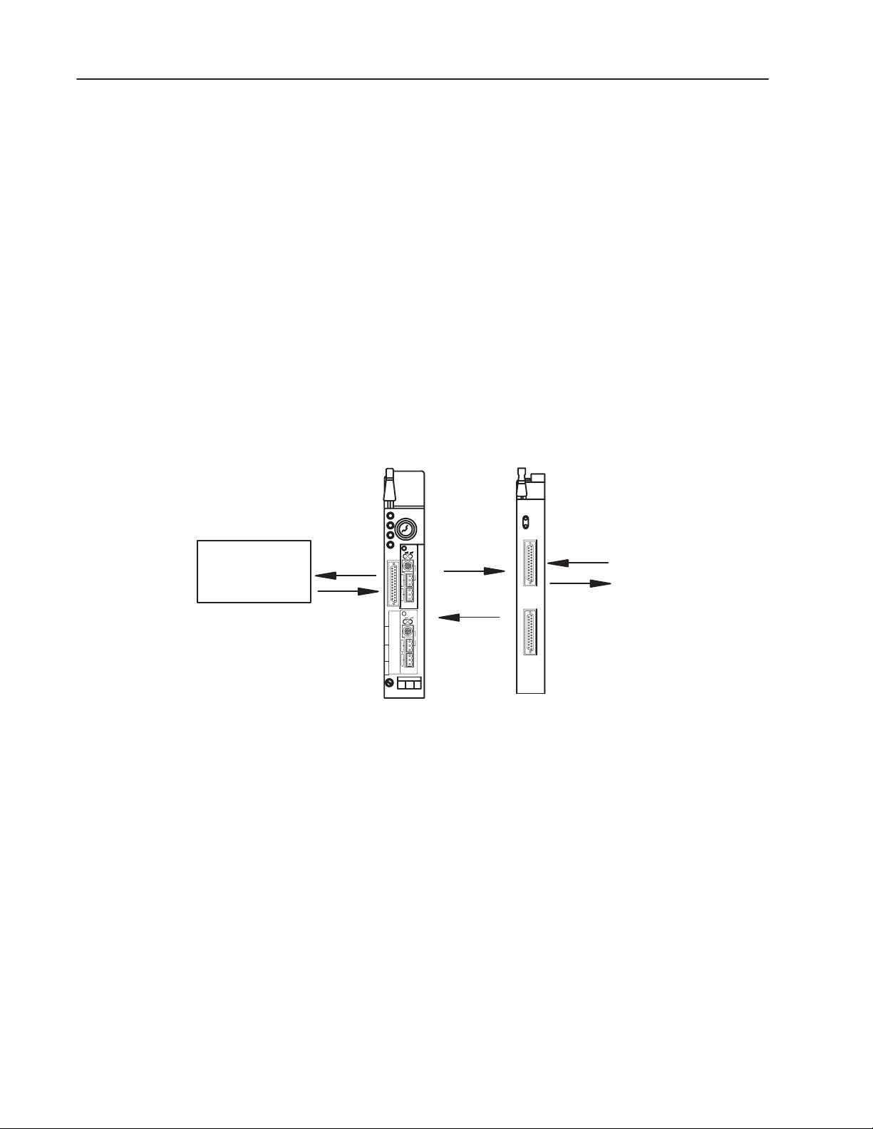
The processor transfers data to and from the module using BTW
(block transfer write) and BTR (block transfer read) instructions in
your ladder diagram program. These instructions let the processor
obtain input values and status from the module, and let you establish
the module’s mode of operation (Figure NO TAG).
1. The processor transfers your configuration data, output data and
calibration values to the module using a block transfer write
instruction.
2. External input devices generate analog signals that are transmitted
to the module. Internal output circuitry generates analog signals
that drive field devices.
3. The module converts the analog signals into binary or BCD
format and stores theses values until the processor requests their
transfer.
Table 1.A
Communication Between the Processor and the Module
3
1
Accuracy
Memory
User Program
PLC Processor
(PLCĆ5/40 Shown)
BTW
BTR
4
High Resolution
Isolated Analog
Module
From input devices
To output devices
2
12933ĆI
4. When instructed by your ladder program, the processor performs
a read block transfer of the values and stores them in a data table.
5. The processor and module determine that the transfer was made
without error, and that input values are within specified range.
6. Your ladder program can use and/or move the data (if valid)
before it is written over by the transfer of new data in a
subsequent transfer.
See chapter 4, “Configuring the Module,” for more information.
The accuracy of each of the high resolution isolated analog modules
is described in Appendix A.
Chapter Summary
Publication 1771ĆUM127B-EN-P - December 2002
In this chapter you read about the functional aspects of the analog
modules and how they communicate with programmable controllers.
Page 19

Installing the Module
Chapter 2
Chapter Objectives
Before You Install Your
Analog Module
This chapter gives you information on:
For information on See page
Before You Install Your Module . ......................
Determining Power Requirements . ................... 2-1
Determining Module Location in the Chassis . ............ 2-2
Installing the Module . ............................. 2-2
Connecting Wiring . ............................... 2-5
Connecting 4-wire sensors . ........................ 2-9
Sourcing input Analog Modules . ..................... 2-10
Making Your Own Cables . .......................... 2-11
Grounding Field Devices . .......................... 2-12
Module Indicators . .................
Before installing your module in the I/O chassis you must:
Action required: Refer to:
Calculate power requirements for the I/O chassis. page 2-1
Determine module location in the I/O Chassis page 2-2
Connect the cable and make wiring connections to the
remote termination panel
page 2-3
2-1
2-13
Electrostatic Damage
Calculate Power
Requirements for the
I/O Chassis
ATTENTION
!
Preventing Electrostatic Discharge
This equipment is sensitive to electrostatic
discharge, which can cause internal damage and
affect normal operation. Follow these guidelines
when you handle this equipment:
• Touch a grounded object to discharge potential
static.
• Wear an approved grounding wriststrap.
• Do not touch connectors or pins on component
boards.
• Do not touch circuit components inside the
equipment.
• If available, use a static–safe workstation.
• When not in use, keep modules in appropriate
static–safe packaging.
Your module receives its power through the 1771 I/O chassis
backplane from the chassis power supply. The maximum current
drawn by the module from this supply ranges from 1.5 to 3.3A,
dependent upon the particular type of module. Refer to the
specifications in appendix A for standard modules.
Publication 1771ĆUM127B-EN-P - December 2002
Page 20

2–2 Installing the Module
N
N
Add this value to the requirements of all other modules in the I/O
chassis to prevent overloading the chassis backplane and/or
backplane power supply.
Determine Module
Location in the I/O Chassis
Install the Analog Module
Place your module in any slot of the I/O chassis except for the
extreme left slot. This slot is reserved for processors or adapter
modules.
Group your modules to minimize adverse affects from radiated
electrical noise and heat. We recommend the following.
• Group analog and low voltage dc modules away from ac modules
or high voltage dc modules to minimize electrical noise
interference.
• Do not place this module in the same I/O group with a discrete
high-density I/O module when using 2-slot addressing. This
module uses a byte in both the input and output image tables for
block transfer.
To install your module in an I/O chassis:
1. First, turn off power to the I/O chassis:
ATTENTIO
!
Remove power from the 1771 I/O chassis
backplane and disconnect the cable from the
module before removing or installing an I/O
module.
• Failure to remove power from the backplane
could cause injury or equipment damage due to
possible unexpected operation.
• Failure to remove power from the backplane
could cause module damage, degradation of
performance, or injury.
Publication 1771ĆUM127B-EN-P - December 2002
ATTENTIO
!
Observe the following precautions when inserting
or removing keys:
• insert or remove keys with your fingers
• make sure that key placement is correct
Incorrect keying or the use of a tool can result in
damage to the backplane connector and possible
system faults.
Page 21
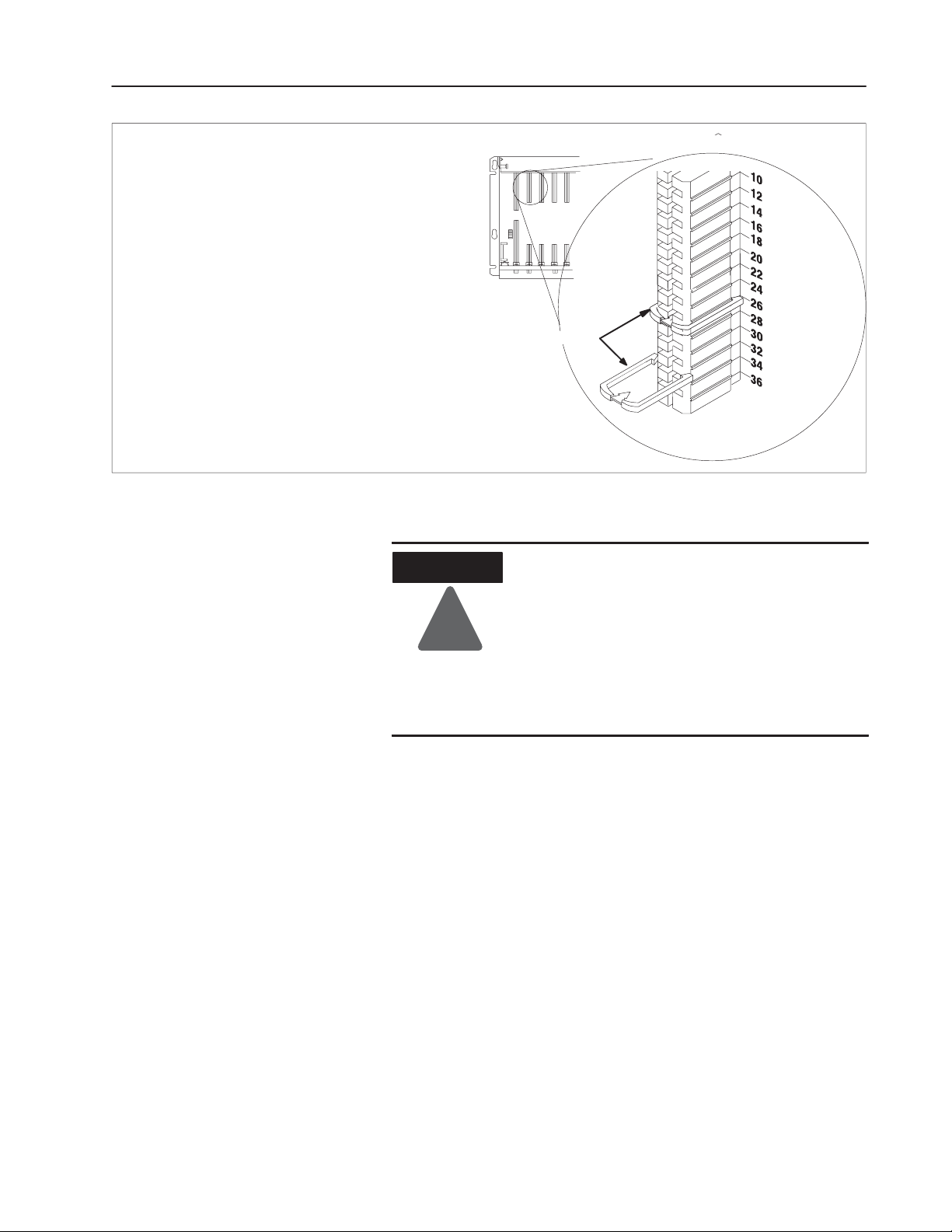
Key the Backplane Connector
N
Place your module in any slot in the chassis
except the leftmost slot which is reserved for
processors or adapters.
Position the keying bands in the backplane connectors
to correspond to the key slots on the module.
Place the keying bands:
between 26 and 28
between 32 and 34
You can change the position of these bands if
subsequent system design and rewiring makes
insertion of a different type of module necessary.
2–3Installing the Module
I/O chassis
Keying Bands
Install the Module in the
Chassis and Connect the
Cable
ATTENTIO
Upper Connector
Remove power from the 1771 I/O chassis
backplane and field wiring arm before removing
or installing an I/O module.
11022ĆI
• Failure to remove power from the backplane or
!
wiring arm could cause module damage, degradation of performance, or injury.
• Failure to remove power from the backplane
could cause injury or equipment damage due to
possible unexpected operation.
1. Place the module in the plastic tracks on the top and bottom of the
slot that guides the module into position.
2. Do not force the module into its backplane connector. Apply firm
even pressure on the module until it is firmly seated in the
chassis. Note: The chassis locking bar will not close if all
modules are not seated properly.
Publication 1771ĆUM127B-EN-P - December 2002
Page 22
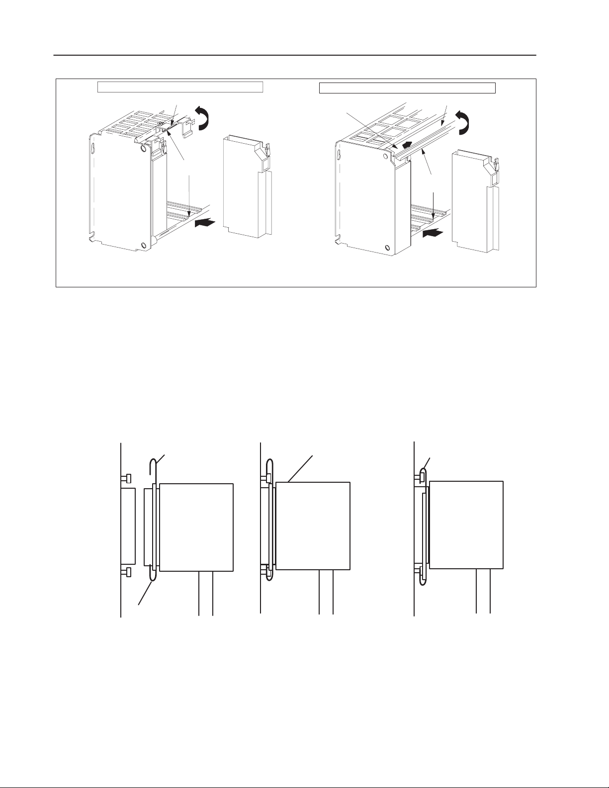
2–4 Installing the Module
1771ĆA1B, ĆA2B, ĆA3B, ĆA3B1, ĆA4B I/O chassis
locking tab
card guides
module
Snap the chassis latch over
the top of the module to secure it.
3. Connect the 1771-NC cable to the module as shown in Figure 2.1.
A. Slide the locking bar up.
B. Insert the cable connector into the mating connector on the
1771ĆA1B, ĆA2B, ĆA3B1, ĆA4B Series B I/O chassis
locking bar pin
Swing the chassis locking bar down into place to secure
the modules. Make sure the locking pins engage.
front of the module.
locking bar
card guides
module
19809
Module Connector
1. Position locking bar in up position.
Cable Connector
Locking bar
C. Slide the locking bar down over the mating pins on the
module to lock the connector onto the module.
Figure 2.1
Connecting the Cable to the Front of the Module
2. Insert connector into mating connector.
3. Slide locking bar down to lock.
11023ĆI
Publication 1771ĆUM127B-EN-P - December 2002
Page 23

2–5Installing the Module
Connecting Wiring
The N-series modules are cable-connected to a remote termination
panel using cat. no. 1771-NC6 (6 ft) or -NC15 (15 ft) cables.
Variations of remote termination panels are used, depending on the
type of module used. These are:
Catalog
Number
1771ĆRTP1 has cold junction compensation for thermocouples
1771ĆRTP3 incorporates resistors and fuses; used primarily for 4Ć20mA inputs
when using +
such as Bussmann GMA-1/4, 250V/250mA.)
1771ĆRTP4 a generalĆuse block with straightĆthru wiring that can be used for all
applications except thermocouples
1771ĆRT41 a 4Ćchannel block with cold junction compensation for thermocouples
1771ĆRT44 a generalĆuse 4Ćchannel block with straightĆthru wiring that can be
used for all applications except thermocouples
1
RTP4 and RT44 can be used withthermocouples if a method of cold junction compensation is provided at
the interface of thermocouple and copper wires within the system.
5V inputs (Uses 5mm x 20mm fast acting 1/4A fuses
Description
1
1
The remote termination panels are designed for mounting on
standard DIN 1 or DIN 3 mounting rails.
Publication 1771ĆUM127B-EN-P - December 2002
Page 24
2–6 Installing the Module
1
3.0
(75.0)
Figure 2.2
Mounting Dimensions for the Remote Termination Panels
RTP1, RTP3, RTP4
AB
Inches
(Millimeters)
2.3
(58.4)
2.3
(58.4)
3.0
(75.0
)
J8
J7
J6
J5
J1
J2
J3
J4
5.30
(134.6)
RT41, RT44
J1
J2
J3
J4
2.3
(58.4)
Dimensions to
3.5
(88.9)
back of DIN rail
19366
Table 2.A
Remote Termination Panel Connection Points for Field Devices (Channel 1 shown)
Input Type Connect To Input Type Connect To Input Type Connect To Input Type Connect To
Voltage
Output
Type
Voltage
+ I1
Ć
Shield S1
Connect To
R1
Current
(with
external
resistor)
Output
Type
+ O1 + O1
R1
Current
Ć
+ I1 + I1 + I1
Ć R1
Shield S1 Shield S1
Connect To Input Type Connect To
Thermocouple
Ć R1
Current
(Source/
Sink)
Shield S1
Power
Excitation (A) O1
Ć R1
RTD
Lead Compensation (B) I1
Shield S1 Shield S1 Common (C) R1
1
When using 4Ćwire RTD, leave the 4th wire open.
2
Not used when NĆSeries module is supplying loop power. Refer to Figure 2.6 in this document.
Publication 1771ĆUM127B-EN-P - December 2002
Ć
Loop
2
R1
O1
Page 25
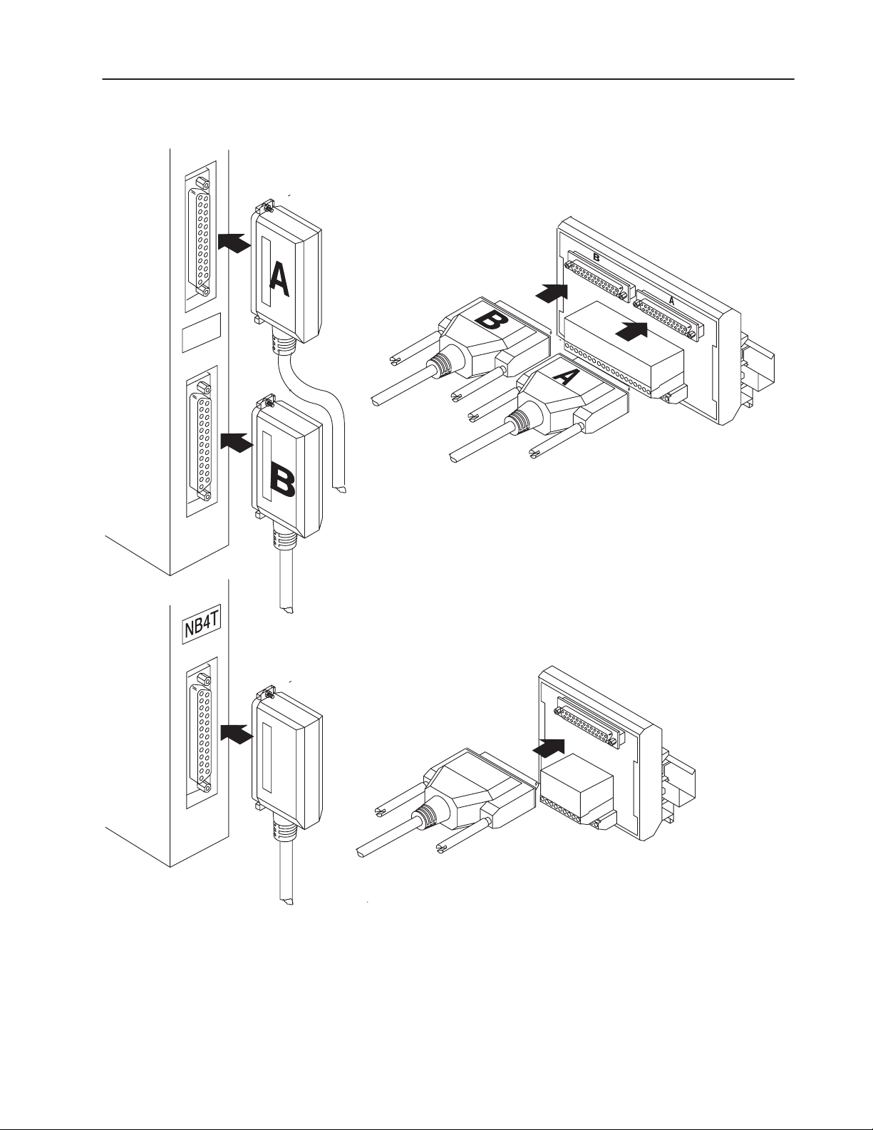
Figure 2.3
Remote Termination Panel Wiring
2–7Installing the Module
Module End of
1771ĆNC cable
Example:
Channel 1 Connections
R1 = Return 1
I1 = Input 1
O1 = Output 1
S1 = Shield 1
RTP End of
1771ĆNC cable
Channel 1 Connections
R1 = Return 1
I1 = Input 1
O1 = Output 1
S1 = Shield 1
Note: Terminals W1, W2 and W3 are
spares.
Do not use terminals CR and CL.
RTP1
DIN Rail
Note: Terminals W1, W2 and W3 are
spares.
Do not use terminals CR and CL.
Module End of
1771ĆNC cable
RT41
RTP End of
1771ĆNC cable
DIN Rail
11024ĆI
Publication 1771ĆUM127B-EN-P - December 2002
Page 26
2–8 Installing the Module
Field wiring to the remote termination panel is the same for all
remote termination panel variations. Refer to Figure 2.4.
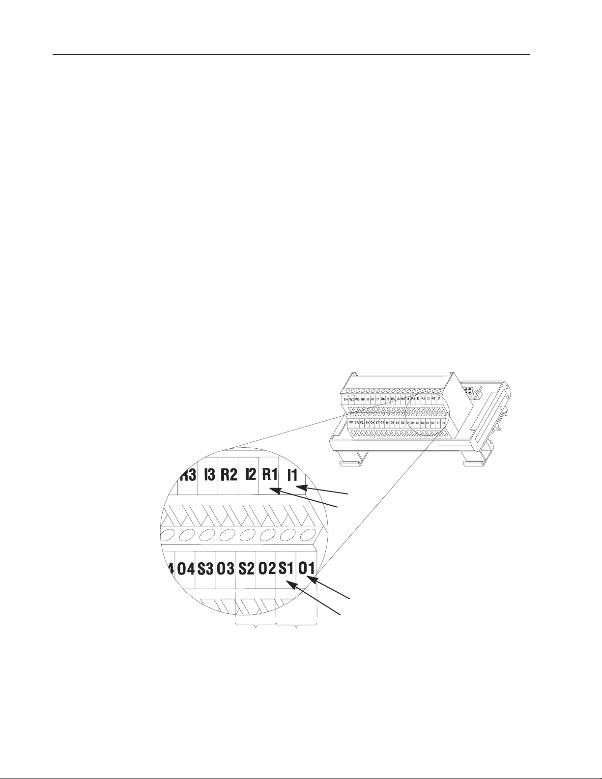
Each channel has 4 connections: R, I, O, and S.
• R = return
• I = input
• O = output
• S = shield
Channel 1 would use R1, I1, O1, and S1; channel 2 would use R2,
I2, O2, and S2; and so on for the remaining channels.
To connect field wiring to the remote termination panel:
1. Strip 3/8 inch (9.25 mm) of insulation from the 22-12 AWG wire.
2. Insert the wire into the open connector slot.
3. Tighten the screw to 4.4–5.2 lb–in. (0.5–0.6Nm) to clamp the
wire.
Figure 2.4
Connecting Wire to the Remote Termination Panel
Each channel has four connections: R, I, O, and S.
Field wiring to the RTP is the same for all RTP variations.
Channel 1 uses R1, I1, O1, and S1; channel 2 uses R2, I2,
O2, and S2; and so on for the remaining channels.
Remote
Termination
Panel (RTP)
I = input
R = return
Field Wiring
O = output
S = shield
Publication 1771ĆUM127B-EN-P - December 2002
channel 2
channel 1
19621
Page 27
2–9Installing the Module
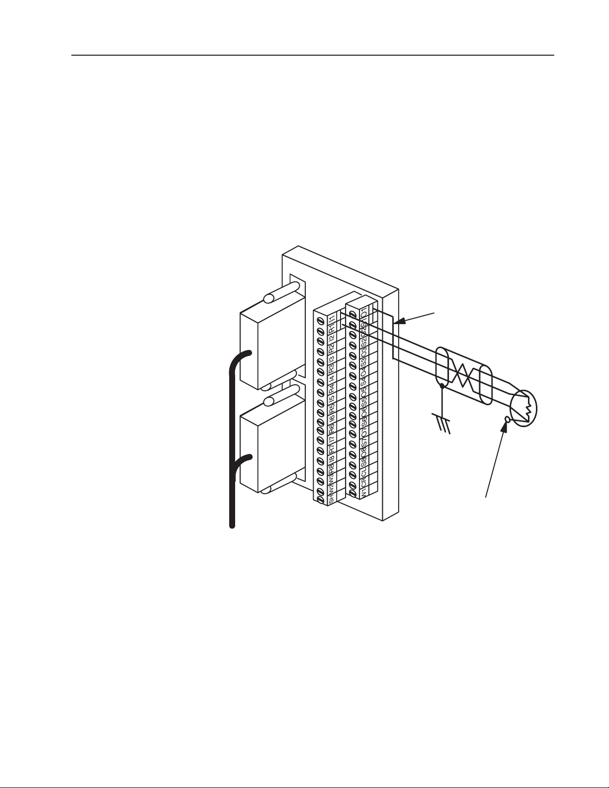
Connecting 4ĆWire
Sensors
Figure 2.5 shows how to connect 4-wire sensors to the remote
termination panel. A 4-wire sensor has two pairs of leads; one pair
for each resistor junction. One wire of the four is not used (it does
not matter which one). This leaves three wires – one pair and one
single wire. You must connect the single wire to the terminal marked
“O_”. You connect the remaining pair of wires to terminals “I_” and
“R_”. It doesn’t matter which wire of the pair connects to terminal
“I_” and which wire connects to terminal “R_” so long as all three
wires are the same AWG gauge.
Figure 2.5
Connecting a 4ĆWire Sensor to the Remote Termination
Panel
Single lead connects
to terminal O
Note: In this illustration:
Terminal O is the 1mA excitation (A) sourcing current
Terminal I is the lead compensation (B) sense input
Terminal R is common (C)
Chassis
Ground
RTD
Leave 1 lead open
12935-I
Publication 1771ĆUM127B-EN-P - December 2002
Page 28
2–10 Installing the Module
Sourcing Input Analog
Modules
The 1771-NIS, 1771-NBSC and 1771-NB4S modules are
sourcing/sinking input modules. These modules can supply the
necessary loop power for 2-wire transmitters connected to the input.
All loop power functionality is contained within the analog module.
Examples of typical configurations are shown in Figure 2.6.
No external resistors are required.
Figure 2.6
Examples of Sourcing/Sinking Input Modules
2ĆWire Transmitter
4ĆWire Transmitter
RTP4
i
Output
Input
Return
Output
24V dc
24V dc
Input
Module supplies loop power
(sourcing)
24V dc
2ĆWire Transmitter
i
24V dc
i
Input
Return
Output
Input
Return
24V dc
Input
Input
User supplies loop power
with 4Ćwire transmitter
(sinking)
User supplies loop power
(sinking)
Inputs can be configured as sourcing or sinking inputs. For sourcing
inputs, the N-series module supplies the loop power. For sinking
inputs, you supply the loop power.
When the loop power is supplied externally, the 16-bit resolution
provides 65535 counts over the 0–20mA current range. This
provides about twice the resolution of voltage inputs with external
resistors.
Publication 1771ĆUM127B-EN-P - December 2002
Page 29

2–11Installing the Module
Thermistor
Making Your Own Cables
Module Top Connector Module Bottom Connector
Channel Number Signal 37ĆPin Connector Wire Color Channel Number Signal 37ĆPin Connector Wire Color
I1 20 Blk I5 20 Blk
1
2
3
O1
R1 21 Wht/Blk R5 21 Wht/Blk
I2 24 Orn I6 24 Orn
O2
R2 25 Wht R6 25 Wht
I3 29 Grn I7 29 Grn
O3
R3 30 Grn/Wht R7 30 Grn/Wht
If you are not using thermocouples, you can terminate the analog
module to a terminal block by cutting the 25-pin RTP end connector
off the standard cable and wiring to your terminal block. Refer to
Table 2.B for wire termination designations.
Table 2.B
Wire Termination Designations
22 Blk/Wht
26 Orn/Blk
31 Grn/Blk
5
6
7
O5 22 Blk/Wht
O6 26 Orn/Blk
O7 31 Grn/Blk
I4 33 Blu I8 33 Blu
4
O4
R4 34 Blu/Wht R8 34 Blu/Wht
35 Blu/Blk
8
Cold Junction
O8 35 Blu/Blk
36 Red
37 Red/Wht
Publication 1771ĆUM127B-EN-P - December 2002
Page 30
2–12 Installing the Module
Grounding the Field
Devices
When using shielded cable or shielded thermocouple extension wire,
ground the foil shield and drain wire only at one end of the cable.
We recommend that you wrap the foil shield and drain wire together
and connect them to the “S” connection on the RTP for the particular
channel. All shield connections are internally connected together in
the RTP so that only one wire is required to ground the entire remote
termination panel. Connect a wire from the “SH” connection on the
RTP to a ground stud on the metal cabinet in which the remote
termination panel is mounted.
If you do not want to ground a particular shield at the RTP, you can
remove the jumper for that particular channel. This will allow the
shield to float at the RTP end. To remove a jumper, you must cut it
out. Once the jumper is removed it cannot be replaced. Clip as
close to the circuit board as possible at both ends to completely
remove it. The jumpers (Figure 2.7) are labeled J1 through J8,
corresponding to channels 1 through 8 respectively.
Figure 2.7
Jumper Positions
Jumpers for channels
5 through 8
J8
J7
J6
J5
J1
J2
J3
J4
Jumpers for channels
1 through 4
Refer to publication 1770-4.1, Programmable Controller Wiring and
Grounding Guidelines, for additional information.
Publication 1771ĆUM127B-EN-P - December 2002
Page 31

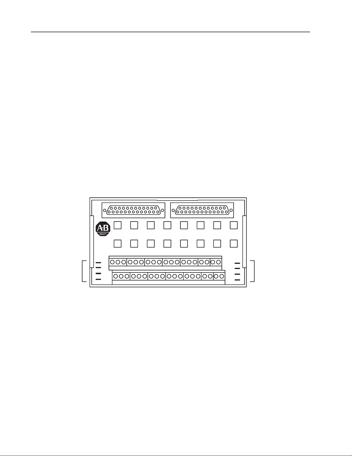
2–13Installing the Module
Interpreting the
Indicator Lights
The front panel of the analog module contains two bi-color
indicators: a red/green RUN/FLT (fault) indicator and a red/green
CAL/COM indicator (Figure 2.8).
Figure 2.8
Diagnostic Indicators
Run/Fault indicator. This indicator will flash green
until the first valid block transfer write has been
RUN/FLT
CAL/COM
received. If a fault is found initially or occurs later, the
RUN/FLT indicator turns red.
Calibrate/communication indicator. This indicator will
flash green when doing block transfers. It will flash red
during calibration.
10528ĆI
At power-up, an initial module self-check occurs. The RUN/FLT
indicator will be green when the check is completed satisfactorily. It
will flash green until the first valid block transfer write has been
received. If a fault is found initially or occurs later, the RUN/FLT
indicator turns red.
Chapter Summary
The bottom indicator is the calibrate/communication indicator. This
indicator will flash green when doing block transfers. It will flash red
during calibration.
Possible module fault causes and corrective action are discussed in
Chapter 7, “Troubleshooting.”
In this chapter you learned how to install your module in an existing
programmable controller system and how to wire to the remote
termination panel.
Publication 1771ĆUM127B-EN-P - December 2002
Page 32

2–14 Installing the Module
Publication 1771ĆUM127B-EN-P - December 2002
Page 33

Chapter 3
Communicating With Your
Analog Module
Chapter Objectives
Block Transfer
Programming
configure the module
send data to the output channels
of those modules having outputs
In this chapter, we describe
• block transfer programming
• quick-startup sample programs for the PLC-3 and PLC-5
processors
• module scan time issues
Your module communicates with the processor through bidirectional
block transfers. This is the sequential operation of both read and
write block transfer instructions.
For the 1771-N series modules, block transfer writes (BTWs) can
perform two different functions.
If you want to: Description This type of BTW is called:
This involves setting the bits which enable the
programmable features of the module, such as
scaling, alarming, real time sampling, etc.
This type of BTW is generally shorter in length
than the configuring BTW because it does not
configure the module each time it is initiated.
the configuration BTW”
the output update BTW"
A configuration BTW is initiated when the analog module is first
powered up, and subsequently only when the programmer wants to
enable or disable features of the module.
An output update BTW is initiated when the programmer wants the
output channels on the module to change value. This shortened
version of the BTW allows faster response time from the output
channels.
The following example programs are minimum programs; all rungs
and conditioning must be included in your application program. You
can disable BTRs, or add interlocks to prevent writes if desired. Do
not eliminate any storage bits or interlocks included in the sample
programs. If interlocks are removed, the program may not work
properly.
Publication 1771ĆUM127B-EN-P - December 2002
Page 34

3–2 Communicating With Your Analog Module
Your analog module works with a default configuration upon
powerup as long as a block transfer write (BTW) has not been
initiated. See the configuration default section in chapter 4 to
understand what this configuration looks like. Refer to the sample
programs in this chapter to get started.
Your program should monitor status bits (such as overrange,
underrange, alarms, etc.) and block transfer read activity.
The following example programs illustrate the minimum
programming required for the 1771-N series module to powerup and
operate.
PLCĆ2 Programming
PLCĆ3 Program Example
Due to the number of digits required for high resolution readings, the
1771-N series modules normally read input values in 2’s complement
binary. Binary coded decimal (BCD) can be used, but with lower
resolution. As a result, the 1771-N series modules are not
recommended for use with PLC-2 family programmable controllers.
Block transfer instructions with the PLC-3 processor use three data
table files. A binary file is used for module location and other related
data. This is the block transfer control file. Two separate block
transfer data files store data that you want transferred to the module
(when programming a block transfer write) or from the module
(when programming a block transfer read). The address of the block
transfer data files are stored in the block transfer control file.
The industrial terminal prompts you to create a control file when a
block transfer instruction is being programmed. The same block
transfer control file is used for both the read and write
instructions for your module. A different block transfer control file
is required for every module.
An example program segment with block transfer instructions is
shown in Figure 3.1, and described below.
Publication 1771ĆUM127B-EN-P - December 2002
Page 35

Figure 3.1
PLCĆ3 Family Sample Program Structure
3–3Communicating With Your Analog Module
Program Action
At powerup, the user program enables a
block transfer read. Then it initiates a
block transfer write to configure module.
Thereafter, the program continuouslyperĆ
forms read and write block transfers.
PLCĆ5 and PLCĆ5/250
Program Example
BTR
BLOCK XFER READ
Block Transfer
1
Read Done Bit
Block Transfer
2
Write Done Bit
RACK:
GROUP:
MODULE:
DATA:
LENGTH:
CNTL:
BTW
BLOCK XFER WRITE
RACK:
GROUP:
MODULE:
DATA:
LENGTH:
CNTL:
X = XXXX
XXXX:XXXX
XXXX:XXXX
X = XXXX
XXXX:XXXX
XXXX:XXXX
XXX
XXX
Enable
EN
12
X
Done
DN
15
00
Error
ER
13
Enable
EN
02
Done
X
DN
05
Error
00
ER
03
This program is very similar to the PLC-3 program with the
following exceptions:
• Block transfer enable bits are used instead of done bits as the
conditions on each rung.
• Separate block transfer control files are used for the block
transfer instructions.
Program Action
At powerup, the user program enables a
block transferread. Thenit initiatesa block
transfer write to configure module.
Thereafter, the program continuously perĆ
forms read and write block transfers.
Figure 3.2
PLCĆ5 Family Sample Program Structure
1
2
BTR Enable
BTR
Enable
BTW Enable
BTW
Enabl
e
BTR
BLOCK XFER READ
RACK:
GROUP:
MODULE:
CONTROL:
DATA FILE:
LENGTH:
CONTINUOUS:
BTW
BLOCK XFER WRITE
RACK:
GROUP:
MODULE:
CONTROL:
DATA FILE:
LENGTH:
CONTINUOUS:
XXX:XX
XXX:XX
XXX:XX
XXX:XX
EN
X
X
DN
X
ER
00
N
EN
X
X
DN
X
ER
00
N
Publication 1771ĆUM127B-EN-P - December 2002
Page 36

3–4 Communicating With Your Analog Module
Module Scan Time
Scan time is defined as the amount of time it takes for the module to
read the input channels and place new data into the data buffer
and/or read the data buffer and write new data to the output channels.
Scan time for your module is shown in Figure 3.3.
Figure 3.3
Block Transfer Time
End of Block
Transfer Write
Block
Transfer
Write
Time
1 2 3 456
Internal scan time = 25ms
Configure
Time
Module available
to perform block transfer
1st Scan 2nd Scan 3rd Scan
The following description references the sequence numbers in
Figure 3.3.
Following a block transfer write (1) the module inhibits
communication until after it has configured the data and loaded
calibration constants (2), scanned the inputs and/or outputs (3), and
filled the data buffer (4). Configuration block transfers, therefore,
should only be performed when the module is being configured or
calibrated.
10529ĆI
Programming Samples
Any time after the buffer is filled (4), a block transfer read (BTR)
request can be acknowledged.
When operated in the default mode, new data will be available for a
BTR every 25 milliseconds. When operated in real time sample
mode
(RTS = T), BTRs will be ignored by the module for “T”
milliseconds, at which time a single BTR will be allowed.
The following are sample programs for using your modules more
efficiently when operating with the PLC-3 or PLC-5 family
processors.
These programs show you how to configure the module and read
data from the module, and efficiently update the output channels on
those modules with outputs.
Refer to the proper PLC-3 or PLC-5 documentation for additional
information on processor programming and data entry.
Publication 1771ĆUM127B-EN-P - December 2002
Page 37

3–5Communicating With Your Analog Module
The differences between the types of 1771-N series modules is
related to the number of output channels each module has. A module
with only inputs (no outputs) requires one BTW after powerup.
Thereafter, it sends back input data and module status by way of
BTRs.
A module with outputs requires BTWs to configure it and update its
output data. BTRs are required to send back input data and module
status.
Sample Ladder Diagram Ć PLCĆ3 Family Processors
The following PLC-3 program can be used for all 1771-N series
modules. The program can be altered to effectively address modules
with or without output channels.
Figure 3.4
PLCĆ3 Family Example Program Structure
Rung 1
Rung 2
Rung 3
Rung 4
BTR
07
BLOCK XFER READ
RACK:
GROUP:
MODULE:
CONTROL:
DATA FILE
LENGTH:
MOV
SOURCE:
DESTINATION:
MOV
SOURCE:
DESTINATION:
BTW
BLOCK XFER WRITE
RACK:
GROUP:
MODULE:
CONTROL:
DATA FILE
LENGTH:
0
0
0
#B1:10
#N1:0
0
0000000000111011
0000000000001001
0000000000001001
0000000000001001
0
0
0
#B1:10
#N1:100
9
Block Transfer
Read Error Bit
B1:10
13
Pushbutton
I0:2
00
Power-up Bit
N1:1
17
Pushbutton
I0:2
00
Block Transfer
Write Error Bit
B1:10
03
Block Transfer
Read Done Bit
B1:10
15
Block Transfer
Write Done Bit
Power-up Bit
N1:1
17
Block Transfer
Write Done Bit
B1:10
05
B1:10
07
Block Transfer
Write Done Bit
B1:10
This program changes the length of the block transfer write from 59 words at powerup
or when reconfigured, to 9 words at all other times.
Enable
EN
12
Done
DN
15
ER
13
B1:0
B1:15
B1:1
B1:15
Enable
EN
Done
DN
Error
ER
03
Error
02
05
Publication 1771ĆUM127B-EN-P - December 2002
Page 38

3–6 Communicating With Your Analog Module
o
Modules without output channels do not require rungs 2 and 3.
Instead, move the input condition instructions from rung 2 to the
front of rung 4, and specify the BTW length equal to 59.
Sample Ladder Diagram Ć PLCĆ5 Family Processors
The following PLC-5 program is very similar to the preceding
PLC-3 program with the following exceptions:
• You use enable bits instead of done bits as the conditions on each
rung.
• A separate control file must be selected for each of the block
transfer instructions.
Figure 3.5
PLCĆ5 Family Example Program Structure
For the following example, assume the analog module is physically located at rack address 01, module group 00, module sl
and the input module connected to the pushbutton is located at rack address 00, module group 7, slot 6. The block transfer
data files correspond to the example on the following pages.
BTR Enable
1
2
3
4
N10:0 N10:5
15
Pushbutton
I:007 N10:5
00 15
Powerup Bit
N10:11
15
Pushbutton
I:007 N10:5
00 15
BTR
Enable
N10:0 N10:5
15 15
BTW Enable
Powerup Bit
N10:11
15
* Length = (number of outputs + 1) words.
For 2 output/6 input modules, this would be equal to 3.
Modules without output channels do not require rungs 2 and 3. Instead, move
the input
condition instructions (pushbutton and powerup) from rung 2 to the front of rung
4, and specify the BTW length equal to 59.
BTR
BLOCK XFER READ
RACK:
15
BTW
Enable
BTW
Enable
BTW
Enable
GROUP:
MODULE:
CONTROL:
DATA FILE:
LENGTH:
CONTINUOUS:
CPT
COMPUTE
DEST
EXPRESSION
CPT
COMPUTE
DEST
EXPRESSION
BTW
BLOCK XFER WRITE
RACK:
GROUP:
MODULE:
CONTROL:
DATA FILE:
LENGTH:
CONTINUOUS:
N10:10
N10:80
N10:0
N10:6
N10:6
N10:5
EN
01
00
DN
0
ER
00
N
59
9
EN
01
00
DN
0
ER
*
N
Publication 1771ĆUM127B-EN-P - December 2002
Page 39

3–7Communicating With Your Analog Module
Setting Up the Data
Table File
Channel 1 400/2000 0/0 1.6 Minimum Ye s N/A
Channel 2 Ć1000/1000 Ć900/900 8.0 User Ye s 100
Channel 3 0/0 25000/26000 17 Ye s 20.0 0.5 N/A N/A B
Scale Value
Low/High
(counts)
Scale Value
Low/High
(counts)
If you use a 1771-NBTC module with the parameters listed below,
the PLC-5 data table file screen on an industrial terminal screen
would look similar to Figure 3.6.
Overall Module Functions Chosen
Number of outputs: 2
Verify mode: Disabled
Temperature Scale: Fahrenheit
BCD Select Bit: 2's complement binary data format
Cold Junction Temperature Alarm: Enabled
Real Time Sampling Rate: 200 milliseconds
Clamp Value
Low/High
(counts)
Alarm Value
Low/High
(counts)
Max Output
Ramp Rate
(mA/sec)
Input Rate
Alarm
o
F/sec)
(
Reset
State
Alarm
Enable
Alarm
Enable
Alarm
Deadband
o
F)
(
Reset
Value
(mA)
Filter
Time
(sec)
10 Ohm
Offset
RTD
TypeTCType
Channel 4 0/0 10000/10500 1.7 Yes 10.0 1.0 N/A N/A E
Channel 5 0/0 20000/20500 1.7 Yes 10.0 1.5 N/A N/A J
Channel 6 0/0 10000/10500 1.7 Yes 10.0 2.0 N/A N/A K
Channel 7 0/0 20000/21000 N/A Ye s 20.0 2.5 N/A N/A R
Channel 8 0/0 30000/31000 N/A Ye s 20.0 3.0 N/A N/A S
The above configuration for the 2 output/6 input module (cat. no.
1771-NBTC) would be set up using the following PLC-5 data table
file (Figure 3.6).
Publication 1771ĆUM127B-EN-P - December 2002
Page 40

3–8 Communicating With Your Analog Module
Figure 3.6
Sample PLCĆ5 Data File (Hexadecimal Data) for a
2 Output/6 Input Module
0
Address
N10:0
N10:10
N10:20
N10:30
N10:40
N10:50
N10:60
N10:70
N10:80
N10:90
N10:100
N10:110
N10:120
N10:130
C684
8800
8010
0062
0000
0000
0000
0000
8820
0000
6590
2000
2710
19C8
1
0000
2000
0C71
0062
0000
0000
0000
0000
04B0
FC18
80AA
0000
2904
5000
Press a function key or enter a
value.
N10:25 =
Rem Prog Forces: None
2
001C
000A
8000
02EC
8010
0EA4
0005
0005
0000
0000
0000
0000
0000
0000
0000
0000
0000
8002
03E8
FC7C
05C8
1000
0000
4E20
1464
801
1
0000
0000
Data: Hex/BCD Addr: Decimal 5/25 Addr 11 APL_NBTC
4
3
000A
6404
0000
39A9
8010
1288
0005
0005
0000
0000
0000
0000
0000
0000
0000
0000
00C8
0190
0384
E032
0000
0000
5014
8011
0000
4000
7918
7530
6
5
003B
0000
39C1
0000
4045
8010
0005
0005
0000
0000
0000
0000
0000
0000
0000
0000
0000
07D0
0000
0064
2904
2710
3000
0E64
0000
4E20
8000
1DC8
8
7
000A
642C
8000
44E6
8010
0000
0000
0000
0000
0000
A00A
0000
61A8
0000
0A64
8011
0000
0000
5208
8000
6000
0000
9
0050
0000
0000
0000
0000
0000
Chapter Summary
Change
Radix
F1
Specify
Address
F5
The block transfer read data file is located at N10:10 thru N10:37.
The block transfer write data file is located at N10:80 thru N10:138.
In this chapter, you learned how to program your programmable
controller. You were given sample programs for your PLC-3 and
PLC-5 family processors, and shown what the data file for a module
looks like.
You also read about module scan time.
Next
File
F7
Prev
File
F8
Publication 1771ĆUM127B-EN-P - December 2002
Page 41

Chapter 4
Configuring the Module
Chapter Objectives
Configuring the High
Resolution Isolated
Analog Modules
In this chapter you will read how to:
• configure your module’s features
• condition your inputs and outputs and
• enter your data.
Because of the many analog devices available and the wide variety
of possible configurations, you must configure your module to
conform to the analog device and specific application that you have
chosen. Data is conditioned through a group of data table words that
are transferred to the module using a block transfer write instruction.
Configure your module for its intended operation by means of your
programming terminal and write block transfers.
Note: Programmable controllers that use 6200 software (release 4.2
or higher) programming tools can take advantage of the IOCONFIG
Addendum utility to configure this module. IOCONFIG Addendum
uses menu-based screens for configuration without having to set
individual bits in particular locations. You must have block
transfer read and block transfer write rungs in your program
before using IOCONFIG software. Refer to your 6200 software
literature for details.
Important: It is strongly recommended that you use IOCONFIG to
configure this module. The IOCONFIG utility greatly
simplifies configuration. If the IOCONFIG is not
available, you must enter data directly into the data
table. Use this chapter as a reference when performing
this task.
Note: Programmable controllers that use process configuration and
operation software (cat. no. 6190-PCO) can take advantage of those
development and runtime tools used for the application of
programmable controllers in process control. The PCO worksheets
and the menu-driven configuration screens and faceplates let you
configure, test/debug and operate the I/O module. Refer to your
6190-PCO software literature for details.
During normal operation, the processor transfers from 1 to 59 words
to the module when you program a BTW instruction to the module’s
address. The BTW file contains configuration words, high and low
channel alarm settings, and calibration values that you enter for each
channel.
Publication 1771ĆUM127B-EN-P - December 2002
Page 42

4–2 Configuring the Module
When making entries in the configuration block, use binary or
hexadecimal only.
Default Configurations
The modules can be operated in a default mode by using zeroes in all
but the first word of the BTW data file. The first word must identify
the number of outputs on the module. For example, the first word
for the 8 output module (cat. no. 1771-NOC) would be 8880
hexadecimal; the first word for the 2 out/6 input module (cat. no.
1771-NBVC, -NBTC, -NBRC) would be 8820 hexadecimal; and the
first word for the 8 input module (cat. no. 1771-NIV, -NT1, -NR)
would be 8800 hexadecimal.
First Word in BTW file
8880 hexadecimal 8
8870 hexadecimal 7
8860 hexadecimal 6
8850 hexadecimal 5
8840 hexadecimal 4
8830 hexadecimal 3
8820 hexadecimal 2
8810 hexadecimal 1
8800 hexadecimal 0
Number of
Outputs
The default scaling values that apply to the inputs and outputs are
listed in the specifications in appendix A. In default mode, all
programmable features (alarming, filtering, real time sampling, etc.)
are disabled.
Publication 1771ĆUM127B-EN-P - December 2002
Page 43

4–3Configuring the Module
Module Level
Programming Features
Module level programming features include:
• module “configuration” verification
• temperature scale
• data format
• real time sample
Module Configuration" Verification
The verify bit 00 in the block transfer write word 3 allows you to
compare the configuration information the module is using to the
configuration information contained in a block transfer write (BTW).
You set the verify bit in the BTW you wish to check, and download
the BTW to the module. After the BTW is completed, request a BTR
from the module. The program verify field in the BTR (bits 09-10
decimal, bits bits 11-12 octal, word 1) will contain either of two
values: 10 (binary) indicates the verify failed; 11 (binary) indicates
the verify succeeded.
If the verify bit is set, configuration information in the BTW data file
will not be used by the module regardless of the success or failure of
the verify.
Temperature Scale
You select the temperature scale that the module will use when
returning temperature to the processor using bit 01, word 3 of the
block transfer write data file. If the bit is set to 0, the temperature is
in degrees C; if the bit is set to 1, the temperature is in degrees F.
Data Format
Use bit 02, word 3 of the block transfer write data file to select a data
format. If this bit is 0, all data fields will be in two’s complement
binary format. If the bit is 1, all fields will be in BCD format. In
BCD, the most significant bit is the sign bit for all signed fields. This
sign bit applies to both BTW and BTR words.
NOTE: Available resolution is poor when using BCD format.
The 4-digit BCD format uses an arrangement of 16 binary digits to
represent a 4-digit decimal number from 0000 to 9999 (Figure 4.1).
The BCD format is used when the input values are to be displayed
for operator viewing. Each group of four binary digits is used to
represent a number from 0 to 9. The place values for each group of
0
digits are 2
group of four binary digits is determined by multiplying the binary
digit by its corresponding place value and adding these numbers.
, 21, 22 and 23 (Table 4.A). The decimal equivalent for a
Publication 1771ĆUM127B-EN-P - December 2002
Page 44

4–4 Configuring the Module
The 1771-N series modules use 15-bit signed magnitude BCD. The
maximum range value available then becomes +
Figure 4.1
4ĆDigit Binary Coded Decimal
Sign Bit Ć
0=+
1X22=4
1
=2
1X2
0
1X2
=1
0111100110011001
Sign
Bit
7
99
1=Ć
7
1X2
0X2
0X2
1X2
3
=8
2
=0
=0
=1
1X2
0X2
0X2
1X2
9
3
=8
2
=0
1
=0
0
=1
1
0
7999.
9
3
1X2
=8
2
0X2
=0
9
1
=0
0X2
0
1X2
=1
9
10
12955ĆI
Table 4.A
BCD Representation
3
(8) 22(4) 21(2) 20(1)
2
Place Value
0 0 0 0 0
0 0 0 1 1
0 0 1 0 2
0 0 1 1 3
0 1 0 0 4
0 1 0 1 5
0 1 1 0 6
0 1 1 1 7
1 0 0 0 8
1 0 0 1 9
Decimal
Equivalent
Publication 1771ĆUM127B-EN-P - December 2002
Page 45

4–5Configuring the Module
Two's Complement Binary
Two’s complement binary is used with PLC-3 processors when
performing mathematical calculations internal to the processor. To
complement a number means to change it to a negative number. For
example, the following binary number is equal to decimal 22.
10110
= 22
2
10
First, the two’s complement method places an extra bit (sign bit) in
the left-most position, and lets this bit determine whether the number
is positive or negative. The number is positive if the sign bit is 0 and
negative if the sign bit is 1. Using the complement method:
0 10110 = 22
To get the negative using the two’s complement method, you must
invert each bit from right to left after the first “1” is detected.
In the above example:
0 10110 = +22
Its two’s complement would be:
1 01010 = -22
Note that in the above representation for +22, starting from the right,
the first digit is a 0 so it is not inverted; the second digit is a 1 so it is
not inverted. All digits after this one are inverted.
If a negative number is given in two’s complement, its complement
(a positive number) is found in the same way:
1 10010 = -14
0 01110 = +14
All bits from right to left are inverted after the first “1” is detected.
The two’s complement of 0 is not found, since no first “1” is ever
encountered in the number. The two’s complement of 0 then is still 0.
Real Time Sampling
Real time sampling is set using word 4 of the block transfer write
data file. The real time sampling (RTS) mode of operation provides
data from the module at a fixed time period for use by the processor.
RTS is invaluable for time based functions (such as PID and
totalization) in the processor. It allows accurate time based
calculations in local or remote I/O racks.
Publication 1771ĆUM127B-EN-P - December 2002
Page 46

4–6 Configuring the Module
In the RTS mode, the module scans and updates its inputs at a user
defined time interval (
module ignores block transfer read (BTR) requests for data until the
sample time period elapses. The BTR of a particular data set
occurs only once at the end of the sample period and subsequent
requests for transferred data are ignored by the module until a new
data set is available. If a BTR does not occur before the end of the
next RTS period, a time-out bit is set in the BTR status area (word
1). When set, this bit indicates that at least one data set was not
transferred to the processor. (The actual number of data sets missed
is unknown.) The time-out bit is reset at the completion of the BTR.
Legal RTS values are in intervals of 1ms from 0.100 to 10.000
seconds in binary format, or 0.100 to 9.999 seconds in BCD format.
An RTS value of 0 disables the real time sampling feature.
∆T) instead of the default interval. The
Output Channel
Programming Features
Output channel programming features include:
• low and high scaling
• low and high clamping
• ramping
• alarm enable
• reset state
• reset value
Scaling
Scaling is the conversion of unscaled data to engineering units. You
use scaling so that the data for each channel is represented in actual
engineering units.
Each channel has two scaling points, low and high. The signal value
at these points is fixed. For example, the high scaling point of a
10V output channel always corresponds to an output signal equal to
+
+10.000V.
Publication 1771ĆUM127B-EN-P - December 2002
Page 47

Channel Type Sensor Low Scaling Point High Scaling Point
5/+55mV Input
100mV Input
650 Ohm Input
10V Output Ć10.0V +10.0V
25mA Output 4mA 20mA
50mA Output 1mA 50mA
5V Input 1.0V 5.0V
10V Input Ć10.0V +10.0V
4Ć20mA Input 4mA 20mA
Ć
Ć
Millivolt Ć5mV +55mV
Temperature Ć300C/Ć508F 1800C/3272F
Millivolt Ć100mV +100mV
Temperature Ć300C/Ć508F 1800C/3272F
Resistance 1.0 Ohm 650 Ohm
Temperature Ć200C/Ć328F 900C/1652F
To implement the scaling feature, you insert the minimum and
maximum scaled values in the appropriate configuration words.
4–7Configuring the Module
Scaling values can be entered in either BCD or binary format. The
range of binary format scaling values is +
7999. Remember to check the data format bit for proper control.
+
32767; BCD format is
For example, assume that at 0mA, the device connected to this input
channel is producing 0 psi, and at 20mA it produces 150 psi.
Extrapolation indicates that at 4mA, the device is producing 30 psi.
By setting the low scale value of the input to 30 and the high scale
value to 150, this input channel will report data in psi.
For better resolution, you can multiply both of the scaling values by
the same multipler as long as both scale values are in the range of
32767 binary or +7999 BCD. By setting the low scale to 3000 and
+
the high scale value to 15000, you would report data in units of 0.01
psi per count.
Maximum resolution can be obtained by setting the low scale value
to -32767 (-7999 in BCD) and the high scale value to +32767 (+7999
in BCD).
Publication 1771ĆUM127B-EN-P - December 2002
Page 48

4–8 Configuring the Module
10V Output
25mA Output
50mA Output
5V Input
10V Input
4Ć20mA Input
5/+55mV Input
100mV Input
650 Ohm Input
If both the low scale and high scale values are set to 0, the module
reports data in the default resolution as shown below.
Channel Type Data Format Temperature Scale Resolution
Binary N/A 0.1mV/count
BCD N/A 1mV/count
Binary N/A 0.1mA
BCD N/A 1mA
Binary N/A 0.1mA
BCD N/A 1mA
Binary N/A 0.1mV
BCD N/A 1mV
Binary N/A 0.1mV
BCD N/A 1mV
Binary N/A 0.1mA
BCD N/A 1mA
Binary Voltage Mode 0.01mV/count
BCD Voltage Mode 1mV/count
Ć
Binary Celsius Mode 0.1oC/count
BCD Celsius Mode 10oC/count
Binary Fahrenheit Mode 0.1oF/count
BCD Fahrenheit Mode 10oF/count
Binary Voltage Mode 0.01mV/count
BCD Voltage Mode 1mV/count
Binary Celsius Mode 0.1oC/count
BCD Celsius Mode 10oC/count
Binary Fahrenheit Mode 0.1oF/count
BCD Fahrenheit Mode 10oF/count
Binary Resistance Mode 0.1 Ohm/count
BCD Resistance Mode 1 Ohm/count
Binary Celsius Mode 0.1oC/count
BCD Celsius Mode 10oC/count
Binary Fahrenheit Mode 0.1oF/count
BCD Fahrenheit Mode 10oF/count
Publication 1771ĆUM127B-EN-P - December 2002
Page 49

4–9Configuring the Module
Clamping
Output channels can be configured to limit or clamp the output
signal at a specified value regardless of the output data value written
to the module. Low and high clamping values are written to the
module in scaled units, and must be within the absolute signal limits
shown below.
Output Type Low Absolute Limit High Absolute Limit
+ 10V Ć10.4V 10.4V
25mA 0mA 26mA
50mA 0mA 50mA
If either value is outside of these limits, or if the low clamp is higher
than the high clamp, the bad programming status bit (bit 07 in BTR
word 1) will be set.
When the clamp feature is activated (output from the programmable
controller is greater than the high clamp or lower than the low
clamp) a corresponding high or low clamp status bit is set in the
channel status word returned in the BTR.
High Clamp Limit
Low Clamp Limit
Figure 4.2Clamped Outputs
Time
output value sent by PLC processor
clamped output value
If the PLC processor commands
the output past the clamp limit,
the module will not output a value
outside the predetermined range.
Clamp the output
so that it cannot exceed
a predetermined range
(high and low clamp limit).
clamp inactive
clamp active
Publication 1771ĆUM127B-EN-P - December 2002
Page 50

4–10 Configuring the Module
Ramping
Output ramping is used to limit the rate of change of an output
channel. You enter the rate as a percentage (between 0 and 200%) of
full scale per second, where 0 disables the ramping feature, and full
scale is the difference between the low and high scaling points. 4.3
shows the effect of ramping on the output signal.
Figure 4.3Ramping on the Output Signal
Ramped OutputOutput Ramp Disabled
Voltage
Voltage
Time
Actual voltage change
Ramped voltage change
Time
Alarm Enable
Clamping and ramping are only active when the alarm enable bit
(decimal bit 17, octal bit 15) has been set to 1.
Reset State
This field determines the action taken by the channel if the I/O reset
backplane pin is asserted.
I/O Reset State Binary Value
Decimal
Last State 0 0
Minimum 0 1
Maximum 1 0
User Selectable 1 1
Octal
Bit 14
(Bit 16)
Bit 13
(Bit 15)
Publication 1771ĆUM127B-EN-P - December 2002
The minimum and maximum values are defined as the low and high
absolute limits respectively.
Page 51

4–11Configuring the Module
Reset Value
If the channel is programmed to go to a user-selectable reset value
upon I/O reset, the value is entered (in scaled units) into that
channel’s proper configuration word. The value entered must be
between the high and low absolute limits. If user-selectable resetting
is not chosen, this field should be set to 0.
Input Channel
Programming Features
Input channel programming includes:
• low and high scaling
• low and high alarming
• alarm deadband
• rate alarming
• alarm enable
• digital filtering
• thermocouple type
• RTD type
• 10 Ohm offset
Scaling
Scaling input channels is identical to scaling output channels. Refer
to “Output Channel Programming Features” on page 4–6.
Alarms
Each input channel has five alarm functions that provide status
indication through five associated status bits in the block transfer
read data returned by the module.
Input alarms let the user specify a range of “good” input values. If
the input value goes outside of this range, and the alarm enable bit is
set, the module will set the low or high alarm bit for that channel.
The alarm values are written to the module in the same units as the
scaling values, and must be within the absolute signal limits
specified in appendix A.
• Underrange - This bit is set if the input falls below the
minimum range for that specific input type. This alarm is
predefined and cannot be changed by the user. In current loop
inputs, this bit also indicates an open loop.
Publication 1771ĆUM127B-EN-P - December 2002
Page 52

4–12 Configuring the Module
• Overrange - This bit is set if the input rises above the
maximum range for that specific input type. This alarm is
predefined and cannot be changed by the user. For all voltage,
RTD and thermocouple inputs, this bit indicates an open
channel.
Alarm Deadband
Alarm deadband allows the user to program a hysteresis effect on the
alarming for a given channel. The deadband cannot be larger than
255 binary or 99 BCD, or 1/2 of the difference between the low
alarm and high alarm values.
• Low Alarm With Deadband - The low alarm bit is set when
the input falls below the user-defined low alarm value. If a
deadband is programmed, the low alarm bit will reset when
the input rises above the level equal to the low alarm value
plus the deadband.
• High Alarm With Deadband - The high alarm bit is set when
the input rises above the user-defined high alarm value. If a
deadband is programmed, the high alarm bit will reset when
the input falls below the level equal to the high alarm value
and deadband.
Overrange Limit
High Alarm Limit
Input Channel
Low Alarm Limit
Underrange Limit
Figure 4.4
Deadband Example
without deadband with deadband
Time
Time
The process passes through
the deadband before the alarm
is disabled to provide stability
to alarm indicators
deadband
deadband
alarm inactive
alarm active
Publication 1771ĆUM127B-EN-P - December 2002
Page 53

High Alarm Limit
Input Channel
4–13Configuring the Module
Rate Alarm
This bit is set when the input changes at a rate faster than the
user-defined value. Rate of change values can range from 0.05% to
50% of the input’s full scale range per second. Full scale range is
defined as the difference between the high scale value and the low
scale value. The rate is specified in scaled units per second.
Figure 4.5
Rate of Change Alarm
Select the change in input
that should activate the alarm
to alert the user of potential
problems.
Low Alarm Limit
alarm inactive
alarm active
Time
Digital Filtering
This value specifies the time constant for a digital first order lag
filter on the input. It is specified in units of 0.1 seconds. Values range
from 0.1-9.9 seconds in BCD and 0.1-10.0 seconds in binary. A
value of 0 disables the filter.
The digital filter equation is a classic first order lag equation
(Figure 4.6). Using a step input change to illustrate the filter
response (Figure 4.7), you can see that when the digital filter
constant time elapses, 63.2% of the total response is reached. Each
additional time constant achieves 63.2% of the remaining response.
Figure 4.6
Digital Filter Equation
t
(X
Yn = Y
n-1
+
t + TA
– Y
n
n-1
)
Where:
Y
n = present output, filtered peak voltage (PV)
Y
n -1 = previous output, filtered PV
t = module channel update time (seconds)
TA = digital filter time constant (seconds)
X
n = present input, unfiltered PV
Publication 1771ĆUM127B-EN-P - December 2002
Page 54

4–14 Configuring the Module
6
Amplitude
Figure 4.7
Digital Filter Lag Equation Illustration
100%
63%
0
Unfiltered Input
TA = 0.01 sec
TA = 0.5 sec
TA = 0.99 sec
0 0.01 0.5 0.99 Time in Seconds
Thermocouple Type
This field lets you select the type of sensor connected to a
thermocouple input channel. This field must be 0 for all other
channel types.
Sensor Type Binary Value
Decimal 15 14 13 12
Octal 17 16 15 14
Millivolt 0 0 0 0
B 0 0 0 1
E 0 0 1 0
J 0 0 1 1
K 0 1 0 0
R 0 1 0 1
S 0 1 1 0
T 0 1 1 1
1
C
1
N
1
For 1771ĆNT2 only.
1 0 0 0
1 0 0 1
1
Publication 1771ĆUM127B-EN-P - December 2002
Page 55

4–15Configuring the Module
0
RTD Type
This field lets you select the type of sensor connected to a 650 ohm
input channel. This field must be 0 for all other channel types.
Sensor Type Binary Value
Decimal 10 09 08
Octal 12 11 10
Resistance 0 0 0
100 Ohm Pt. European Std. 0 0 1
100 Ohm Pt. U.S. Std. 0 1 0
10 Ohm Copper 0 1 1
120 Ohm Nickel 1 0 0
10 Ohm Offset
This field lets you compensate for a small offset error in a 10 ohm
copper RTD. Values can range from -0.99 to +0.99 ohms in units of
0.01 ohms.
Configuration Block for a
Block Transfer Write
Word/Dec. Bit
Word/Octal Bit
15 14 13 12 11 10 09 08 07 06 05 04 03 02 01 00
17 16 15 14 13 12 11 10 07 06 05 04 03 02 01 00
For example, if the resistance of a copper RTD used with this
o
channel was 9.74 ohms at 25
C, you would enter -0.26 in this field.
The configuration block for a block transfer write consists of:
• module configuration header
• output channel data (if applicable)
• output channel programming (if applicable)
• input channel programming (if applicable)
Block Transfer Write Configuration Data Header
The configuration data header consists of information required for
the processor to properly identify the type of information it will be
receiving.
Module Configuration Data Header
BTW word type Constant Number of outputs Constant
1 0 0 0 1 0 0 0 0 0 1 0 0 0 0 0
Publication 1771ĆUM127B-EN-P - December 2002
Page 56

4–16 Configuring the Module
Bit/Word Description of Word 0
Word Bit Definition
Word 0 00Ć03 Constant = 0
Bits 04Ć07 Number of outputs = 0010
Bits 10Ć15 Constant = 00 1000
Bits 16Ć17 Block transfer write type = 10
The next group of words sets the outputs of the module, if the
module has outputs. For example, if this is a 2 output/6 input
module, words 1 and 2 would contain the data for the two output
channels. If the module has four outputs, words 1 thru 4 would
contain output channel data.
Output Configuration Words 1 and 2
Word/Dec. Bit
Word/Octal Bit
1 Channel 1 Output Data
2 Channel 2 Output Data
15 14 13 12 11 10 09 08 07 06 05 04 03 02 01 00
17 16 15 14 13 12 11 10 07 06 05 04 03 02 01 00
Bit/Word Description of Output Configuration Words 1 and 2
Word
Word 1 Bits 00Ć15 (00Ć17) First Output channel data
Word 2 Bits 00Ć15 (00Ć17) Second Output channel data
Decimal Bit
(Octal Bit)
Additional module configuration data is contained in the next two
words. This includes verify, temperature scale, BCD select, cold
junction alarm enable and real time sample time. These are explained
in the bit/word description.
Output Configuration Words 3 and 4
Word/Dec. Bit
15 14 13 12 11 10 09 08 07 06 05 04 03 02 01 00
Definition
Word/Octal Bit
3
4 RTS Sample Time: 1 millisecond units
Publication 1771ĆUM127B-EN-P - December 2002
17 16 15 14 13 12 11 10 07 06 05 04 03 02 01 00
CJ alarm
enable
Unused = 0
BCD
select
Temp
scale
Verify
Page 57

Bit/Word Description of Output Configuration Words 3 and 4
4–17Configuring the Module
Word
Word 3 Bit 00
Word 4
Decimal Bit
(Octal Bit)
Verify. If this bit is set to 1, the module will compare its current
programming with the programming downloaded in the BTW. If
they are the same, it will verify good; if they are different, the
module will verify bad. In no case will any programming data in
the BTW be applied to the module.
Bit 01 Temperature scale. 0 = Celsius, 1 = Fahrenheit
Bit 02
Bits 03Ć14
(03Ć16)
Bit 15 (17)
Bits 00Ć15
(00Ć17)
BCD select. 1 = all values in BCD format.
Not used. Always 0
CJ alarm enable. A value of 1 enables over and underrange
indication for the cold junction channel. If the module does not
have a cold junction channel, this bit is 0.
Real time sample. Sample time in milliseconds.0=off.
RTS minimum is 100msec (counts = 100). Maximum 10
seconds in binary; 9.999 seconds in BCD.
Definition
0 = all values in 2's complement binary
Output Programming
The next group of six words contain channel-specific parameters.
This includes low and high scale values, low and high clamp values,
ramp rate, reset state, alarm enable and reset value.
Output Configuration Words 5 through 10
Word/Dec. Bit
Word/Octal Bit
5 Low Scale Value
6 High Scale Value
7 Low Clamp Value
8 High Clamp Value
9
10 Reset Value
15 14 13 12 11 10 09 08 07 06 05 04 03 02 01 00
17 16 15 14 13 12 11 10 07 06 05 04 03 02 01 00
Channel 1 Programming
Alarm
enable
Reset State 0 Maximum Ramp Rate, % of Full Scale per second
Publication 1771ĆUM127B-EN-P - December 2002
Page 58

4–18 Configuring the Module
Bit/Word Description of Output Configuration Words 5 through 10
Word
Word 5
Word 6
Word 7
Word 8
Word 9
Word 9
continued
Decimal Bit
(Octal Bit)
Bits 00Ć15
(00Ć17)
Bits 00Ć15
(00Ć17)
Bits 00Ć15
(00Ć17)
Bits 00Ć15
(00Ć17)
Bits 00Ć11
(00Ć13)
Bit 12 (14) Constant = 0
Bits 13Ć14
(15Ć16)
Low scale value for channel 1. Scale values are limited to
32767 in binary format; +7999 in BCD format.
+
High scale value for channel 1. Scale values are limited to
32767 in binary format; +7999 in BCD format.
+
Low clamp value for channel 1. The channel output will not be
allowed to go below this value (in scaled units) regardless of
the data sent to the module. Clamp values are limited to
32767 in binary format; +7999 in BCD format.
+
High clamp value for channel 1. The channel output will not be
allowed to go above this value (in scaled units) regardless of
the data sent to the module. Clamp values are limited to
32767 in binary format; +7999 in BCD format.
+
Maximum ramp rate. If this field is not 0, the module will limit
the maximum rate of change for this channel to be a
percentage of the full scale range of the module. Legal values
are from 1 to 200%.
Reset state. This field controls what an output channel will go
to if the I/O reset line is asserted:
00 binary = last state;
01 binary = minimum output; (example: < Ć10V, < 4mA)
10 binary = maximum output; (example: > 10V, > 22mA)
11 binary = user reset value.
Definition
Bit 15 (17)
Word 10
Bits 00Ć15
(00Ć17)
The above six words of output channel-specific information would
be repeated for the next output channel (2), as shown below. The
bit/word descriptions would be the same as above.
Word/Dec. Bit
Word/Octal Bit
11 Low Scale Value
12 High Scale Value
13 Low Clamp Value
14 High Clamp Value
15
16 Reset Value
15 14 13 12 11 10 09 08 07 06 05 04 03 02 01 00
17 16 15 14 13 12 11 10 07 06 05 04 03 02 01 00
Channel 2 Programming
Alarm
enable
Reset State 0 Maximum Ramp Rate, % of Full Scale per second
Alarm enable. If set to 1, the module reports high clamp, low
clamp and rate limit. If 0, these warnings are suppressed.
Reset value. If the user selects the channel to go to a user
reset value upon I/O reset, the value in scaled units is entered
here. Otherwise, set to 0.
Publication 1771ĆUM127B-EN-P - December 2002
Page 59

4–19Configuring the Module
The following six words configure the first input channel of the
module. These words are repeated as necessary for each input in the
module. For example, if this is a 2 output/6 input module, words 1
through 4 would configure the module, words 5 through 16 would
configure the 2 output channels (six words each). Then six groups of
seven words each (one group for each input channel) would
configure the module’s six input channels.
Input Programming
Word/Dec. Bit
Word/Octal Bit
17 Low Scale Value
18 High Scale Value
19 Low Alarm Value
20 High Alarm Value
21
22 Filter Time Constant: 0.1 second units Alarm Deadband
23 Thermocouple Type 0 RTD Type 10 Ohm Offset: 0.01 Ohm units
15 14 13 12 11 10 09 08 07 06 05 04 03 02 01 00
17 16 15 14 13 12 11 10 07 06 05 04 03 02 01 00
Channel 3 Programming
Alarm
enable
Rate Alarm: Scaled Units per second
Bit/Word Description of Input Configuration Words 17 through 23
Word
Word 17
Word 18
Decimal Bit
(Octal Bit)
Bits 00Ć15
(00Ć17)
Bits 00Ć15
(00Ć17)
Definition
Low scale value for channel 3.
High scale value for channel 3.
Word 19
Word 20
Word 21
Word 22 Bits 00Ć07
Bits 00Ć15
(00Ć17)
Bits 00Ć15
(00Ć17)
Bits 00Ć14
(00Ć16)
Bit 15 (17)
Low alarm value for channel 3.
High alarm value for channel 3.
Rate alarm. If the channel's input changes at a rate faster than this value and
the alarm enable bit is set, the channel will indicate a rate alarm condition.
Legal values are from 0.05 to 50% of full scale per second.
Alarm enable bit. If set to 1, the module will report high alarm, low alarm,
underrange, overrange, and rate alarm conditions. If 0, these warnings
are suppressed.
Alarm deadband. This field creates a hysteresis effect on the low and high
alarms. For an alarm condition to be removed, the input signal must go above
the low alarm limit or below the high alarm limit by an amount equal to the
specified deadband. Alarm deadband values must be less than or equal to
one half the difference of the high and low alarm values.
Publication 1771ĆUM127B-EN-P - December 2002
Page 60

4–20 Configuring the Module
Word 23
Word
Decimal Bit
(Octal Bit)
Bits 8Ć15
(10Ć17)
Bits 00Ć07
Bits 08Ć10
(10Ć12)
Bit 11 (13) Constant = 0
Bits 12Ć15
(14Ć17)
Filter time constant. Specifies the time constant of a digital, first order lag filter
on the input in 0.1 second units. Legal values are 0.1 to 10.0 seconds
(binary) or 0.1 to 9.9 (BCD). A value of 0 disables the filter.
10 ohm offset. Compensates for a resistance offset on a 10 ohm copper
RTD. Range of +
other RTDs.
RTD type. Specifies type of RTD linearization on RTD channels:
001 = 100 ohm Pt, European standard;
010 = 100 ohm Pt. US standard;
011 = 10 ohm copper;
100 = 120 ohm nickel.
This field is 0 for nonĆRTD channels.
Thermocouple type. Specifies type of TC linearization on TC channels.
0000 = millivolts;
0001 = B;
0010 = E;
0011 = J;
0100 = K;
0101 = R;
0110 = S;
0111=T;
1000= C (1771ĆNT2 only),
1001= N (1771ĆNT2 only).
This field must be 0 for nonĆthermocouple channels.
Definition
0.99 ohms, in units of 0.01 ohms. This field must be 0 for all
Chapter Summary
The above group of words would be repeated for each of the
remaining five input channels. The bit/word descriptions would be
identical for each of those channels.
Refer to the Appendix specific to your module for block transfer
write configurations to be used with your module.
In this chapter you learned how to configure your module’s
hardware, condition your inputs and enter your data.
Publication 1771ĆUM127B-EN-P - December 2002
Page 61

Chapter 5
Module Status and Input Data
Chapter Objectives
Reading Data from the
Module
In this chapter you will read about:
• reading data from your module
• block transfer read data format
Block transfer read (BTR) programming moves status and data from
the module to the processor’s data table in one I/O scan. The
processor user program initiates the request to transfer data from the
module to the processor.
The transferred words contain module status, channel status and
input data from the module. The maximum BTR data file length
required is 28 words.
Block transfer reads are defined for each type of module platform,
rather than type of outputs/inputs. The types of modules are:
Possible Combinations Appendix
8 out/0 in C
7 out/1 in K
6out/2in I
5out/3in J
4 out/4 in H
3 out/5 in G
2 out/6 in E
1out/7in F
0 out/8 in B
2 out/2 in D
For example, the BTR from the 1771-NB4T (two 0-25mA out/two
thermocouple in) is identical to the BTR for the 1771-NB4S (two
0-25mA out/two 4-20mA in), since both are 2 input/2 output
modules.
When you perform a BTR for a specific module, the bits for fields
that do not pertain to your specific module are set to zero.
Complete block transfer read data formats and bit/word descriptions
for your particular module are shown in the Appendices.
Publication 1771ĆUM127B-EN-P - December 2002
Page 62

5–2 Module Status and Input Data
Block Transfer Read
Data Format
The block transfer read data format consists of an initial block
header which identifies the type of module (input, output, or
output/input), and groups of words that contain information on either
an input channel or an output channel.
Output channel words are configured immediately after the block
header. If the module contains both output and input channels, the
output channel words come first in the block transfer read data
format.
Outputs Only" Block Transfer Read Data Header
This header is used for modules with outputs only (such as cat. no.
1771-NOC and 1771-NOV).
Word/Dec. Bit
Word/Octal Bit
0 Constant = 8800 Hexadecimal
1
2 Constant = 8000 Hexadecimal
3 Unused = 0
15 14 13 12 11 10 09 08 07 06 05 04 03 02 01 00
17 16 15 14 13 12 11 10 07 06 05 04 03 02 01 00
Power
up
Bad
Chan.
Data
Mod
Alarm
RTS
Time
out
I/O
Reset
Program
Verify
Mod
Fault
Bad
Prog
Bad
Struct
Unused = 0
The bit/word descriptions for the “outputs only” header block are
shown below.
Word
Word 0 Bits 00Ć15
Word 1
Decimal Bit
(Octal Bit)
(00Ć17)
Bit 00-05
Bit 06
Bit 07
Bit 08 (10)
Bits 09Ć10
(11Ć12)
Bit 11 (13)
Definition
Always 8800 Hexadecimal
Not used. Always 0
Bad structure. This bit is set if there is an error in the BTW
header.
Bad program. This bit is set if any of the module level
programming data is illegal.
Module fault. This bit is set if any of the programming data sent
to the module in the most recent BTW was illegal, or if one or
more channels has the bad calibration bit set.
Program verify. Indicates the result of verify request.
00 = verify not requested;
10 = verify failed;
11 = verify succeeded
I/O reset. This bit is set whenever the I/O reset line on the
backplane is asserted.
Publication 1771ĆUM127B-EN-P - December 2002
Bit 12 (14)
RTS timeout. This bit is set if a BTR was not requested of the
module within the RTS sample time.
Page 63

5–3Module Status and Input Data
Word/Dec. Bit
Word
Word 1 continued
Word 2 Always 8000 hexadecimal.
Word 3 Not used. Always 0
Decimal Bit
(Octal Bit)
Bit 13 (15)
Bit 14 (16)
Bit 15 (17)
Module alarm. This bit is set if there is an alarm bit set for one
or more channels. The input alarm bits are low, high alarm and
rate alarm. The output channel alarm bits are low and high
clamp, and the rate limit alarm.
Bad channel data. This bit is set if the module is in BCD mode
and one or more of the input data values sent in the last BTW
are not legal BCD values.
Powerup bit. This bit is set until a BTW with programming data
is received by the module.
Definition
Inputs Only" and Output/Input" Block Transfer Read
Data Header
This following three-word header is used if the module only has
input channels, or if it contains both input and output channels.
15 14 13 12 11 10 09 08 07 06 05 04 03 02 01 00
Word/Octal Bit
0 Constant = 8800 Hexadecimal
1
2 1 Unused = 0
3 Cold Junction Temperature; Units of 0.01 degrees C or 0.1 degrees F
17 16 15 14 13 12 11 10 07 06 05 04 03 02 01 00
Power
up
Bad
Chan.
Data
Mod
Alarm
RTS
Time
out
I/O
Reset
Program
Verify
Mod
Fault
Bad
Prog
Bad
Struct
Unused = 0
The bit/word descriptions for the “inputs only” and “output/input”
header block are shown below.
Word
Word 0
Word 1
Decimal Bit
(Octal Bit)
Bits 00Ć15
(00Ć17)
Bits 00Ć05 Not used
Bit 06
Bit 07
Always = 8800 hexadecimal
Bad structure. This bit is set if there is an error in the BTW
header.
Bad program. This bit is set if any of the module level
programming data is illegal.
Definition
CJC
Over
Range
CJC
Under
Range
Publication 1771ĆUM127B-EN-P - December 2002
Page 64

5–4 Module Status and Input Data
Word
Word 1 continued
Decimal Bit
(Octal Bit)
Bit 08 (10)
Bits 09Ć10
(11Ć12)
Bit 11 (13)
Bit 12 (14)
Bit 13 (15)
Bit 14 (16)
Bit 15 (17)
Bit 00
Definition
Module fault. This bit is set if any of the programming data sent
to the module in the most recent BTW was illegal, or if one or
more channels has the bad calibration bit set.
Program verify. Indicates the result of verify request. 00 = verify
not requested; 10 = verify failed; 11 = verify succeeded
I/O reset. This bit is set whenever the I/O reset line on the
backplane is asserted.
RTS timeout. This bit is set if a BTR was not requested of the
module within the RTS sample time.
Module alarm. This bit is set if there is an alarm bit set for one
or more channels. The input alarm bits are low, high alarm and
rate alarm. The output channel alarm bits are low and high
clamp, and the rate limit alarm.
Bad channel data. This bit is set if the module is in BCD mode
and one or more of the input data values sent in the last BTW
are not a legal BCD value.
Powerup bit. This bit is set until a BTW with programming data
is received by the module.
Cold junction compensation (CJC) underrange bit. This bit is
set if the CJC temperature is below 0
o
C.
Word/Dec. Bit
Word/Octal Bit
Cold junction compensation (CJC) overrange bit. This bit is set
if the CJC temperature is above 70
Not used. Always 0
Cold junction temperature. Units of 0.01 degrees C or 0.1
degrees F. (0.1 degrees C or 1.0 degrees F in BCD.)
o
C.
Word 2
Word 3
Bit 01
Bits 02Ć14
(02Ć16)
Bit 15 (17) Always = 1
Bits 00Ć15
(00Ć17)
Input Status Data
Each input channel has two words associated with it. One word
provides underrange, overrange, low and high alarms, rate alarm,
bad program and bad calibration information to the processor. The
second word contains channel input data. These words would
immediately follow the header on modules containing only inputs, or
after the output channel words on modules containing both outputs
and inputs.
15 14 13 12 11 10 09 08 07 06 05 04 03 02 01 00
17 16 15 14 13 12 11 10 07 06 05 04 03 02 01 00
Channel 1 Status
4 1 Unused = 0 Bad
5 Channel 1 Input Data
Publication 1771ĆUM127B-EN-P - December 2002
Calib
Bad
Prog
0 Rate
Alarm
High
Alarm
Low
Unused = 0 Over
Alarm
Range
Under
Range
Page 65

5–5Module Status and Input Data
The above two words would be repeated for each input channel. For
example, if this module had two input channels, the following words
would be used.
Word/Dec. Bit
Word/Octal Bit
4 1 Unused = 0 Bad
5 Channel 1 Input Data
6 1 Unused = 0 Bad
7 Channel 2 Input Data
15 14 13 12 11 10 09 08 07 06 05 04 03 02 01 00
17 16 15 14 13 12 11 10 07 06 05 04 03 02 01 00
Channel 1 Status
Bad
Calib
Prog
Channel 2 Status
Bad
Calib
Prog
Bit/word descriptions for the input status data words are shown
below.
Bit/Word Description for Input Status Data Words
Word
Decimal Bit
(Octal Bit)
Bit 00
Bit 01
0 Rate
Alarm
0 Rate
Alarm
Underrange bit. This bit is set if the input signal is below the
input channels minimum range.
Overrange bit. This bit is set if the input signal is above the
input channels maximum range.
High
Alarm
High
Alarm
Low
Alarm
Low
Alarm
Definition
Unused = 0 Over
Range
Unused = 0 Over
Range
Under
Range
Under
Range
Word 4
Word 5
Bits 02-03 Not used. Always 0
Bit 04
Bit 05
Bit 06
Bit 07 Not used. Always 0
Bit 08 (10)
Bit 09 (11)
Bits 10Ć14
(12Ć16)
Bit 15 (17) Not used. Always = 1
Bits 00Ć15
(00Ć17)
Low alarm. This bit is set if alarms are enabled and the input
data is lower than the low alarm setpoint.
High alarm. This bit is set if alarms are enabled and the input
data is higher than the high alarm setpoint.
Rate alarm. This bit is set if the input signal changed at a rate
faster than the input rate alarm setpoint.
Bad program. This bit is set if any of the channel level
programming data is illegal.
Bad calibration. This bit is set if the channel has not had a valid
calibration.
Not used. Always 0
Channel 1 input data.
Publication 1771ĆUM127B-EN-P - December 2002
Page 66

5–6 Module Status and Input Data
Output Status Data
Each output channel also has two words associated with it. The first
word contains low and high clamp, rate alarm, bad data, bad program
and bad calibration information for the processor. This is followed
by raw count data for that channel. If the module contains both input
and output channels, the output channel words would immediately
follow the header words.
Word/Dec. Bit
Word/Octal Bit
4 Unused = 0 Bad
5 Channel 1 Raw Count sent to DAC
15 14 13 12 11 10 09 08 07 06 05 04 03 02 01 00
17 16 15 14 13 12 11 10 07 06 05 04 03 02 01 00
Channel 1 Status
Bad
Bad
Calib
Prog
Data
The above two words would be repeated for each output channel. For
example, if this module had two output channels, the following
words would be used.
Word/Dec. Bit
Word/Octal Bit
4 Unused = 0 Bad
5 Channel 1 Raw Count sent to DAC
6 Unused = 0 Bad
7 Channel 2 Raw Count sent to DAC
15 14 13 12 11 10 09 08 07 06 05 04 03 02 01 00
17 16 15 14 13 12 11 10 07 06 05 04 03 02 01 00
Channel 1 Status
Bad
Bad
Calib
Prog
Data
Channel 2 Status
Bad
Bad
Calib
Prog
Data
Rate
Alarm
Rate
Alarm
Rate
Alarm
High
Clamp
High
Clamp
High
Clamp
Low
Clamp
Low
Clamp
Low
Clamp
Unused = 0
Unused = 0
Unused = 0
Publication 1771ĆUM127B-EN-P - December 2002
Page 67

Bit/Word Description for Output Status Data Words
5–7Module Status and Input Data
Word
Word 4
Word 5
Decimal Bit
(Octal Bit)
Bit 00-03 Not used. Always 0
Bit 04
Bit 05
Bit 06
Bit 07
Bits 08 (10)
Bit 09 (11)
Bits 10Ć15
(12Ć17)
Bits 00Ć15
(00Ć17)
Low clamp. This bit is set if alarms are enabled and the output
data is lower than the low clamp value.
High clamp. This bit is set if alarms are enabled and the output
data is higher than the high clamp value.
Rate alarm. This bit is set if alarms are enabled and the output
data changed faster than the programmed ramp rate.
Bad data. This bit is set if BCD format was chosen and the
output data is not a legal BCD value.
Bad programming. This bit is set if the most recent BTW
contained improper programming data for this channel
Bad calibration. This bit is set if the channel has not had a
valid calibration.
Not used. Always = 0
Channel 1 Raw data sent to DAC.
Definition
Refer to the Appendix specific to your module for block transfer
read configurations.
Chapter Summary
In this chapter you learned the meaning of the status information that
the modules send to the processor.
Publication 1771ĆUM127B-EN-P - December 2002
Page 68

5–8 Module Status and Input Data
Publication 1771ĆUM127B-EN-P - December 2002
Page 69

Module Calibration
Chapter 6
Chapter Objective
Tools and Equipment
Tool or Equipment Description
Precision Voltage Source 0-10V, 1µV resolution
Precision Resistors
OR
Precision Decade
Resistor Box
In this chapter we tell you how to calibrate your module. Your
module is shipped from the factory already calibrated. This
chapter tells you how to recalibrate or change calibration.
In order to calibrate your analog module you will need the following
tools and equipment:
High Precision Resistors:
649 ohm, 0.01%, 5ppm/
1 ohm, 0.1%, 5ppm/
Accuracy: Minimum three decades;
Decade one - 10 ohm decade, 1 ohm per step, better than 0.005 ohms (0.5% accuracy)
Decade two - 100 ohm decade, 10 ohm per step, better than 0.005 ohms (0.05% accuracy)
Decade three - 1000 ohm decade, 100 ohm per step, better than 0.01% accuracy
Any vendor's model that meets or exceeds the above specifications can be used. The user is
responsible for assuring that the decade box maintains accuracy by periodic calibration as specified by
the vendor. As a service to its customers, AllenĆBradley offers this partial list of vendors who can supply
decade resistor boxes that meet or exceed the specifications.
o
o
C
Lower Precision Resistors:
If calibration to rated accuracy is not required, lower precision resistors
C
can be used. Add percentage of tolerance and temperature coefficient
error for expected accuracy. Refer to 6.A and 6.B below.
Precision Multimeter
Industrial Terminal and
Interconnect Cable
Electro Scientific Industries
Portland, OR
Series DB 42
50mA, 1µA resolution
10V, 1µV resolution
Programming terminal for A-B family processors
IET Labs
Westbury, NY
HARS-X Series
If calibration to rated accuracy is not required, lower precision
resistors can be used. Add the percentage of tolerance and the
temperature coefficient error for expected accuracy.
Resistor Accuracy
Resistors change value over time. Both load life and temperature
reduce the accuracy. The best way to determine the resistance of a
resistor is to measure its value to the accuracy needed under the
conditions in which it is used.
Julie Research Labs
New York, NY
DR 100 Series
Publication 1771ĆUM127B-EN-P - December 2002
Page 70

6–2 Module Calibration
Table 6.A
Resistor Tolerance vs. Expected Error
Resistor Tolerance Expected Error
0.1% 0.1%
0.5% 0.5%
1.0% 1.0%
Note: If the tolerance error of the 649 ohm resistor is > than
18 ohms (2.8%), calibration will fail.
+
Table 6.B
Temperature Coefficient Error
Calibrating Your Module
Temperature
Coefficient of
Resistor
25ppm/oC10
50ppm/oC10
200ppm/oC10
nT (Calibration
temperature
deviation from 25
5oC 0.081 ohms (0.012%)
20oC 0.325 ohms (0.05%)
5oC 0.162 ohms (0.025%)
20oC 0.649 ohms (0.1%)
5oC 0.649 ohms (0.1%)
20oC 2.596 ohms (0.4%)
o
C)
o
C 0.162 ohms (0.025%)
o
C 0.325 ohms (0.05%)
o
C 1.298 ohms (0.2%)
Expected Error
Example: Using a 649 ohm resistor, rated for 1% accuracy, with a
o
temperature coefficient of 50ppm/
of 1.05% (1.0% plus 0.05%) when calibration is done at 35
o
C).
of 10
C, provides an expected accuracy
o
C (nT
The analog module is shipped already calibrated. If it becomes
necessary to recalibrate the module, you must calibrate the module in
an I/O chassis. The module must communicate with the processor
and an industrial terminal.
Publication 1771ĆUM127B-EN-P - December 2002
Calibration service is available from Allen–Bradley. Contact your
local sales office or field support center for information on how to
send your module in for calibration. Modules under warranty will be
calibrated at no charge. Modules out of warranty, sent in for
calibration only, will be calibrated for less than the standard repair
charge.
Before calibrating the module, you must enter ladder logic into the
processor memory, so that you can send block transfer data to the
module, and the processor can read block transfer data from the
module.
Calibration can be accomplished using any of three methods:
Page 71

6–3Module Calibration
T
• manual calibration – refer to the procedure below.
• 6200 I/O CONFIG software – refer to your 6200 software
publications (release 4.2 or later) for procedures for calibrating.
• PCO operator interface software – refer to your 6190-PCO
software publications for procedures for calibrating.
Indicator Operation During Calibration
During calibration, the RUN/FLT indicator will turn to green. The
CAL/COM indicator will turn to flashing red. The indicators will
remain with these indications throughout the calibration procedure.
Manual Calibration
Word/Dec. Bit
Word/Octal Bit
15 14 13 12 11 10 09 08 07 06 05 04 03 02 01 00
17 16 15 14 13 12 11 10 07 06 05 04 03 02 01 00
You can calibrate any number of channels, in any order. The
following procedures define how to calibrate input and output
channels.
In order to allow the module to stabilize,
IMPORTAN
energize the module for at least 30 minutes
before calibrating.
Set up a block transfer write data file as shown in table 6.C.
Input Channel Calibration
1. Set the appropriate bit in the BTW input calibration mask (word
2); channel 1 is bit 00, channel 2 is bit 01, etc. If calibrating only
one channel, set the appropriate bit. If calibrating all channels (all
inputs), set bits (00 through 07). Refer to Table 6.C.
Table 6.C
Calibration Block Transfer Write
0 Calibration BTW Header = CC00 Hexadecimal
Cal
1 Unused = 0
2 Unused = 0 Input Cal Mask
3 Unused = 0 Output Cal Mask
4 1st Low Output Cal Value
5 1st High Output Cal Value
6 2nd Low Output Cal Value
7 2nd High Output Cal Value
8 3rd Low Output Cal Value
Publication 1771ĆUM127B-EN-P - December 2002
Clk
High/
Low
Page 72

6–4 Module Calibration
Word/Dec. Bit
Word/Octal Bit
9 3rd High Output Cal Value
10 4th Low Output Cal Value
11 4th High Output Cal Value
12 5th Low Output Cal Value
13 5th High Output Cal Value
14 6th Low Output Cal Value
15 6th High Output Cal Value
16 7th Low Output Cal Value
17 7th High Output Cal Value
18 8th Low Output Cal Value
19 8th High Output Cal Value
2. Apply the appropriate low reference signal (Table 6.D) to all
input channels being calibrated (for channel 1, I1 on RTP).
Table 6.D
Calibration Reference Signal Values
00010203040506070809101112131415
00010203040506071011121314151617
Type Low Reference Value High Reference Value
5 Volt input 0.0000V 5.0000V
10V input 0.0000V 10.0000V
4-20mA sourcing input 1.000mA 21.000mA
-5 to 55mV/TC input 0.000mV 55.000mV
100mV/TC input 0.000mV 100.000mV
650 Ohm RTD input 1.000 Ohms 649.0 Ohms
10V output 0.000V 10.000V
25mA output 0.500mA 22.000mA
50mA output 1.000mA 50.000mA
Publication 1771ĆUM127B-EN-P - December 2002
Page 73

Figure 6.1
Connecting a Resistor or Decade Resistance Box to the Remote
Termination Panel
Connect the resistor across terminals
R1-I1 and O1.
640 ohm resistor for
high reference value.
1 ohm resistor for low
reference value.
If using a decade resistance box,
connect in place of the resistor
6–5Module Calibration
Decade resisĆ
tance box
12935-I
3. Send a block transfer write to the module with word 1 containing
CAL CLK bit (01) = 1, and HI/LO bit (00) = 0.
4. Send a block transfer write to the module with word 1 containing
CAL CLK bit (01) = 0, and HI/LO bit (00) = 0.
Publication 1771ĆUM127B-EN-P - December 2002
Page 74

6–6 Module Calibration
Table 6.E
Calibration Block Transfer Read
Word/Dec. Bit
Word/Octal Bit
0 Calibration BTR Header = C000H
1 Unused = 0 Range EEPROM
2 Input Cal Done bits
3 Output Cal Done bits
4 Input Bad Cal bits
5 Output Bad Cal bits
6 Corrected Channel 1 Data
7 Corrected Channel 2 Data
8 Corrected Channel 3 Data
9 Corrected Channel 4 Data
10 Corrected Channel 5 Data
11 Corrected Channel 6 Data
12 Corrected Channel 7 Data
13 Corrected Channel 8 Data
15 14 13 12 11 10 09 08 07 06 05 04 03 02 01 00
17 16 15 14 13 12 11 10 07 06 05 04 03 02 01 00
5. Apply the appropriate high reference signal (Table 6.D) to all
input channels being calibrated (for channel 1, I1 on RTP).
6. Send a block transfer write to the module with word 1 containing
CAL CLK bit (01) = 1, and HI/LO bit (00) = 1.
7. Send a block transfer write to the module with word 1 containing
CAL CLK bit (01) = 0, and HI/LO bit (00) = 1.
8. Request a block transfer read (BTR) from the module. If the
INPUT BAD CAL bit (block transfer read word 4, bit 00, for
channel 1 for example) is reset, and the INPUT CAL DONE bit
(BTR word 2, bit 00 for channel 1 for example) is set, the
procedure is complete.
If the bad BTW bit (word 1, bit 00) is set any time during the
calibration procedure, an error occurred during the calibration
procedure. Repeat the calibration.
Bad
BTW
Publication 1771ĆUM127B-EN-P - December 2002
If the EEPROM bit (word 1, bit 01) is set, the module has a
hardware fault. The module cannot be calibrated.
If the RANGE bit (word 1, bit 02) is set, the channel(s) did not
calibrate because one of the reference signals was out of range.
Repeat the procedure. If the RANGE bit is set a second time,
either the channel is bad, or there is a problem with the
calibration equipment.
Page 75

6–7Module Calibration
Output Channel Calibration
1. Set the appropriate bit in the BTW output calibration mask (word
3); channel 1 is bit 0, channel 2 is bit 01, etc. If calibrating only
one channel, set the appropriate bit. If calibrating the entire
module (all outputs), set all bits (00 through 07).
2. Send a block transfer write to the module with word 1 containing
CAL CLK bit (01) = 1, and HI/LO bit (00) = 0 and all output cal
values = 0.
3. Send a block transfer write to the module with
CAL CLK bit (01) = 0, and HI/LO bit (00) = 0 and all
output cal values = 0.
4. Measure the signal on the channel you are calibrating. Use the
appropriate equation below to calculate the output cal low value
for this channel. Record this value for later use. Do not enter it
into the BTW file at this time.
10V Output
Y = (X x 6000) - 30000
Where: X = meter reading in volts
Y = output cal low/high value
25mA Output
Y = x 60000 - 30000
Where: X = meter reading in mA
Y = x 60000 - 30000
Where: X = meter reading in mA
5. Send a block transfer write to the module with word 1 containing
CAL CLK bit (01) = 1, and HI/LO bit (00) = 1 and all output cal
values = 0.
6. Send a block transfer write to the module with CAL CLK bit (01)
= 0, and HI/LO bit (00) = 0 and all output cal values = 0.
7. Measure the signal on the channel you are calibrating. Use the
appropriate equation above (step 4) to convert the value to the
output cal high value for this channel. Record this value for
later use. Do not enter it into the BTW file at this time.
(X - 0.500)
[
[
21.500
Y = output cal low/high value
50mA Output
(X - 1.000)
49.000
Y = output cal low/high value
]
]
Publication 1771ĆUM127B-EN-P - December 2002
Page 76

6–8 Module Calibration
8. Enter the first set of calculated low and high values into the first
channel output cal values of the block transfer write calibration
data file. If you are calibrating more than one output channel
simultaneously, enter the output cal values from the lowest
numbered output channel in the first output cal value slots. The
next lowest channel in the output mask goes in the second slot of
output cal values, and so on.
9. Send a block transfer write to the module with word 1 containing
CAL CLK bit (01) = 1, and HI/LO bit (00) = 1.
10.Send a block transfer write to the module with word 1 containing
CAL CLK bit (01) = 0, and HI/LO bit (00) = 1.
11. Request a block transfer read (BTR) from the module.
If the OUTPUT BAD CAL bit (word 5, bit 00, for channel 1 for
example) is reset, and the OUTPUT CAL DONE bit (word 3, bit
00 for channel 1 for example) is set, the procedure is complete.
If the bad BTW bit is set any time during the calibration
procedure, an error in the calibration procedure. Repeat the
calibration.
Chapter Summary
If the EEPROM bit is set, the module has a hardware fault. The
module cannot be calibrated.
If the RANGE bit (word 1, bit 02) is set, the channel(s) did not
calibrate because one of the reference signals was out of range.
Repeat the procedure. If the RANGE bit is set a second time,
either the channel is bad, or there is a problem with the
calibration equipment.
In this chapter, you learned how to calibrate your module’s channels.
Publication 1771ĆUM127B-EN-P - December 2002
Page 77

Troubleshooting
Chapter 7
Chapter Objective
Diagnostics Reported by
the Module
We describe how to troubleshoot your module by observing
indicators and by monitoring status bits reported to the processor.
At power-up, the module turns the RUN/FLT indicator to red, then
checks for:
• correct RAM operation
• EPROM operation
• EEPROM operation
After passing initial diagnostics, the module turns the RUN/FLT
indicator to flashing green. The indicator will continue to flash green
until it receives a valid BTW. After the BTW, it will stay solid green
during operation. It will turn red if it detects a fault condition. If the
RUN/FLT indicator is red, block transfers will be inhibited.
The lower CAL/COM indicator flashes green when the module is
communicating with the processor. The speed of the flashing is
dependent upon system speed. If the module is accessed in less than
100ms intervals, the CAL/COM indicator will be solid red.
The module also reports status and specific faults (if they occur) in
every transfer of data to the processor. Monitor the green/red
indicators and status bits in the appropriate word of the BTR file
when troubleshooting your module.
RUN/FLT
CAL/COM
11027-I
Figure 7.1
Indicators
Indicator When Green When Red
flashes - during initial powerĆup
RUN/FAULT
CAL/COM
solid - first valid block transfer write
successfully completed
flashes - when communication is taking
place between the PLC processor and
the NĆseries module.
Publication 1771ĆUM127B-EN-P - December 2002
solid - a fault is found
flashes - during
calibration
Page 78

7–2 Troubleshooting
Both indicators are OFF
RUN/FLT indicator ON red
Troubleshooting with
the Indicators
Indication Probable Cause Recommended Action
RUN/FLT indicator is
flashing green
RUN/FLT indicator is solid green Initial block transfer write successfully completed
Table 7.A shows indications, probable causes and recommended
actions to correct common faults which may occur.
Table 7.A
Troubleshooting Chart
No power to module
Possible short on the module
LED driver failure
Microprocessor, oscillator or EPROM failure
If immediately after power-up, indicates RAM or
EPROM failure.
If during operation, indicates possible
microprocessor or backplane interface failure.
Internal fuse bad
Power-up diagnostics successfully completed.
Check power to I/O chassis.
Recycle as necessary.
Replace module.
Normal operation.
CAL/COM indicator is green
(solid or flashing)
CAL/COM indicator is green and
RUN/FLT indicator is green but
module data is wrong (for
example, with cable off, input
channel data values are at
minimum scale values)
Status Reported by
the Module
Normal operation None required
Internal module problem Replace module
Design your program to monitor module and channel status bits, and
to take appropriate action depending on your application
requirements. You may also want to monitor these bits while
troubleshooting with your industrial terminal. The module sets a bit
(1) to indicate it has detected one or more of the following module
conditions as shown in Table 7.B.
The module sets a bit (1) to indicate it has detected one or more of
the following input channel conditions (Table 7.D), or output channel
conditions (Table 7.C).
Publication 1771ĆUM127B-EN-P - December 2002
Page 79

Table 7.B
Module Status Reported in BTR Word 1
7–3Troubleshooting
Decimal Bit
(Octal Bit)
Word 1 Bit 00Ć05 Not used
Bit 06 Bad structure. This bit is set if there is an error in the BTW header.
Bit 07 Bad program. This bit is set if any of the module level programming
data is illegal.
Bit 08 (10) Module fault. This bit is set if any of the programming data sent to the
module in the most recent BTW was illegal, or if one or more channels
has the bad calibration bit set.
Bits 09Ć10
(11Ć12)
Program verify. Indicates the result of verify request. 00 = verify not
requested; 10 = verify failed; 11 = verify succeeded
Bit 11 (13) I/O reset. This bit is set whenever the I/O reset line on the backplane
is asserted.
Bit 12 (14) RTS timeout. This bit is set if no BTR was requested of the module
within the RTS sample time.
Bit 13 (15) Module alarm. This bit is set if there is an alarm bit set for one or more
channels. The input alarm bits are low, high alarm and rate alarm. The
output channel alarm bits are low and high clamp, and the rate limit
alarm.
Bit 14 (16) Bad channel data. This bit is set if the module is in BCD mode and
one or more of the input data values sent in the last BTW are not a
legal BCD value.
Explanation
Bit 15 (17) Powerup bit. This bit is set until a BTW with programming data is
received by the module.
Word 2 Bit 00 CJC Underrange bit. This bit is set if the CJC temperature is below the
input channel minimum range.
Bit 01 CJC Overrange bit. This bit is set if the CJC temperature is above the
input channel maximum range.
Publication 1771ĆUM127B-EN-P - December 2002
Page 80

7–4 Troubleshooting
Table 7.C
Output Channel Status Word (1 per output channel)
Decimal Bit
(Octal Bit)
Bit 04 Low clamp. This bit is set if alarms are enabled and the output data is
lower than the low clamp value.
Bit 05 High clamp. This bit is set if alarms are enabled and the output data is
higher than the high clamp value.
Bit 06 Rate alarm. This bit is set if alarms are enabled and the output data
changed faster than the programmed ramp rate.
Bit 07 Bad data. This bit is set if BCD data format was chosen and the output
data was not a legal BCD value.
Bit 08 (10) Bad program. This bit is set if any of the channel level programming
data is illegal.
Bit 09 (11) Bad calibration. This bit is set if the channel has not had a valid
calibration.
Table 7.D
Input Channel Status Word (1 per input channel)
Decimal Bit
(Octal Bit)
Bit 00 Underrange bit. This bit is set if the input signal is below the input
channels minimum range.
Definition
Definition
Chapter Summary
Bit 01 Overrange bit. This bit is set if the input signal is above the input
channels maximum range.
Bit 04 Low alarm. This bit is set if alarms are enabled and the input signal is
lower than the low alarm setpoint.
Bit 05 High alarm. This bit is set if alarms are enabled and the input signal is
higher than the high alarm setpoint.
Bit 06 Rate alarm. This bit is set if alarms are enabled and the input signal
changed at a rate faster than the input rate alarm setpoint.
Bit 08 (10) Bad program. This bit is set if any of the module level programming
data is illegal.
Bit 09 (11) Bad calibration. This bit is set if the channel has not had a valid
calibration.
In this chapter, you learned how to interpret the status indicators,
status words and troubleshoot your analog module.
Publication 1771ĆUM127B-EN-P - December 2002
Page 81

Specifications
General Specifications
Appendix A
Number of Channels
(depends on specific module)
I/O Chassis Location any single I/O module slot
A/D Resolution 16 bits or 15 bits plus sign bit
D/A Resolution 14 bits or 13 bits plus sign bit
Input Filtering 6 pole, low pass hardware filter
Calibration Interval 1 year
Isolation Voltage
Maximum Backplane Current and
Power Dissipation @ 5V
8 individually isolated, or
4 individually isolated
Designed to withstand 1000V dc continuous between input and
output channels and between input and backplane connections.
Modules are 100% tested at 1200V dc for 1 second between input
channels and backplane connections.
Current Power
1771ĆNBRC 1.8A 8.5W
1771ĆNB4S 1.6A 7.0W
1771ĆNB4T 1.5A 5.0W
1771ĆNBSC 3.0A 13.0W
1771ĆNBTC 1.6A 7.5W
1771ĆNBV1 1.8A 8.0W
1771ĆNBVC 1.8A 8.5W
1771ĆNIS 2.9A 12.0W
1771ĆNIV 1.5A 6.0W
1771ĆNIV1 1.5A 6.0W
1771ĆNIVR 1.5A 6.0W
1771ĆNIVT 1.5A 5.5W
1771ĆNOC 2.9A 14.0W (20mA)
3.3A 16.0W (25mA)
1771ĆNOV 2.1A 10.0W
1771ĆNR 1.5A 6.0W
1771ĆNT1 1.5A 5.0W
1771ĆNT2 1.5A 5.0W
Environmental Conditions
Operational Temperature IEC 60068-2-1 (Test Ad, Operating Cold)
Storage Temperature IEC 60068-2-1 (Test Ab, Unpackaged, Nonoperating Cold)
Relative Humidity IEC 60068-2-30 (Test Db, Unpackaged, Nonoperating Damp Heat)
Shock
Operating
Nonoperating
IEC 60068-2-2 (Test Bd, Operating Dry Heat)
IEC 60068-2-14 (Test Nb, Operating Thermal Shock)
32 to 140°F(0to60°C)
Ambient changes > 0.5
performance during periods of change.
IEC 60068-2-2 (Test Bb, Unpackaged, Nonoperating Dry Heat)
IEC 60068-2-14 (Test Na, Unpackaged, Nonoperating Thermal
Shock)
-40 to 185°F (-40 to 85°C)
5 to 95% noncondensing
IEC 60068-2-27 (Test Ea, Unpackaged Shock)
30g
50g
o
C per minute may temporarily degrade
Publication 1771ĆUM127B-EN-P - December 2002
Page 82

SpecificationsA–2
Vibration IEC 60068-2-6 (Test Fc, Operating)
2g @ 10-500Hz
ESD Immunity IEC 61000-4-2
4kV contact discharges
Radiated RF Immunity IEC 61000-4-3
10V/m with 1kHz sine-wave 80% AM from 30MHz to 1000MHz
10V/m with 200Hz 50% Pulse 100% AM at 900MHz
EFT/B Immunity IEC 61000-4-4
1kV @ 5kHz on signal ports
+
Surge Transient Immunity IEC 61000-4-5
2kV line-earth (CM) on shielded ports
+
Conducted RF Immunity IEC 61000-4-6
10V rms with 1kHz sine wave 80% AM from 150kHz to 30MHz
Emissions CISPR 11
Group 1, Class A (with appropriate enclosure)
Enclosure Type None (open style
Connecting Cable(s)
1771ĆNC6 = 1.8m (6ft)
1771ĆNC15 = 4.6m (15ft)
Field Wiring Arm Wiring
Size
Insulation
Category
14-22AWG (2.5-0.25mm2) solid or stranded copper wire rated at
o
60
C or greater
3/64 inch (1.2mm) maximum
1
2
Keying
Certifications
(when product is marked)
Between 26 and 28
Between 32 and 34
UL UL Listed Industrial Control Equipment
CSA CSA Certified Process Control Equipment
2
European Union 89/336/EEC EMC Directive,
CE
compliant with:
EN 61000-6-4, Industrial Emissions
EN 50082-2, Industrial Immunity
EN 61000-6-2, Industrial Immunity
EN 61326, Meas./Control/Lab., Industrial Requirements
2
Australian Radiocommunications Act,compliant
C-Tick
with AS/NZS 2064, Industrial Emissions
1 Use this conductor category information for planning conductor routing . Refer to publication 1770Ć4.1, Industrial Automation Wiring and
Grounding Guidelines."
2 See the Product Certification link at www.ab.com for Declarations of Conformity, Certificates, and other certification details.
Publication 1771ĆUM127B-EN-P - December 2002
Page 83

(selectable)
Specifications A–3
Temperature Specifications
±100mV Thermocouple Input -5 to +55mV Thermocouple Input 1Ć650Ω RTD Input
Input Range
Maximum Input Resolution
1
Default Display Resolution 0.01mV / 0.1°C (0.1°F) 0.1mV / 1.0°C (0.1°F) 0.01 ohm / 0.1°C (0.1°F)
Temperature Scale (per module) °C(°F) °C(°F) °C(°F)
Input Impedance >10MΩ >10MΩ
Thermocouple Linearization IPTSĆ68 standard, NBS MNĆ125 IPTSĆ68 standard, NBS MNĆ125
Cold Junction Compensation 0to70°C ±0.25°C 0to70°C ±0.25°C
Open Input Detection upscale upscale upscale
Open TC Leakage Current < 10 nA (maximum) < 10 nA (maximum)
Time to Detect Open Input 10s (maximum) 5s (maximum) 5s (maximum)
RTD Excitation Current 1mA (typical)
Input Overvoltage Protection 140V ac rms continuous 140V ac rms continuous 140V ac rms continuous
Normal Mode Rejection (50/60Hz) 50dB / 60dB (minimum) 50dB / 60dB (minimum) 50dB / 60dB (minimum)
Common Mode Rejection (60Hz) 150dB (typical) 150dB (typical) 150dB (typical)
Offset Drift (maximum) ±0.50µV/°C ±0.50µV/°C ±25 mΩ/°C
Gain Drift (maximum) ±35ppm/°C ±35ppm/°C ±50ppm/°C
Input Bandwidth 9Hz 9Hz 9Hz
Update Time (per module) 25ms (maximum) 25ms (maximum) 25ms (maximum)
Settling Time to within
0.1% of Full Scale
NonĆlinearity 0.02% of full range (maximum) 0.02% of full range (maximum) 0.02% of full range (maximum)
Accuracy with Calibration
(includes nonĆlinearity, gain,
offset)
Calibration Values 0.000 / 100.000mV 0.000 / 55.000mV 1.00 / 649.0Ω
Underrange Threshold -103.0mV -5.5mV 0.9Ω
Overrange Threshold +103.0mV +56.0mV 650Ω
Rate Alarm Value
Minimum (0.04% FSR)
Maximum (50% FSR)
Scaling Points →
Default Scaling Values
1
Maximum resolution is obtained by rescaling input data to counts.
2
These resolutions apply to the commonly used ranges for these thermocouples. See graphs.
3
Values shown are applicable when using 2's complement data format.
3
±105mV -5.5 to 56.0mv 4to650Ω
Type B: 300 to 1800oC (572 to 3272oF)
Type E: -270 to 1000
Type J: -210 to 1200
Type K: -270 to 1372
Type R: -50 to 1768
Type S: -50 to 1768
Type T: -270 to 400
3.3µV/bit @ 15 bits with sign bit
Type E, J, K, T 0.1°C (0.2°F)
Type B, R, S: 0.3oC (0.6oF)
o
C (-454 to 1832oF)
o
C (-346 to 2192oF)
o
C (-454 to 2502oF)
o
C (-58 to 3214oF)
o
C (-58 to 3214oF)
o
C (-454 to 752oF)
2
2
Type B: 300 to 1800oC (572 to 3272oF)
Type C: 0 to 2315
Type E: -20 to 735
Type J: -37 to 966
Type K: -71 to 1372
Type N: -270 to 1300
Type R: -50 to 1768
Type S: -50 to 1768
Type T: -73 to 400
0.95µV/bit @ 16 bits unipolar
Type E, J, K, T, N: 0.03°C (0.06°F)
Type B, R, S: 0.1oC (0.2oF)
Type C: 0.07oC (0.1oF)
o
C (32 to 4199oF)
o
C (-4 to 1355oF)
o
C (-34 to 1770oF)
o
C (-95 to 2502oF)
o
C (-450 to 2372oF)
o
C (-58 to 3214oF)
o
C (-58 to 3214oF)
o
C (-99 to 752oF)
2
2
2
100Ω Pt a=0.00385 European standard:
-200 to +870
100Ω Pt a=0.003916 U.S. standard:
-200 to +630
10Ω copper:
-200 to +260
120Ω nickel:
-80 to +320
10mΩ/bit @ 16 bits unipolar
100Ω Pt & 120Ω Ni 0.03 °C (0.06°F)
10Ω Cu 0.3°C (0.5°F)
125ms (maximum) 125ms (maximum) 125ms (maximum)
0.01% of full range @ 25°C (typical)
0.05% of full range @ 25°C (maximum)
0.08mV / 0.9°C (1.6°F) per second
100mV / 1050°C (1890°F) per second
-100/+100mV → -10000/+10000
-300/1800°C → -3000/18000
-508/3272°F → -5080/32720
0.01% of full range @ 25°C (typical)
0.05% of full range @ 25°C (maximum)
24uV / 0.9°C (1.6°F) per second
30mV / 1050°C (1890°F) per second
-5/+55mV → -500/+5500
-300/1800°C → -3000/18000
-508/3272°F → -5080/32720
0.025% of full range @ 25°C (typical)
0.05% of full range @ 25°C (max.)
0.26Ω / 0.44°C (0.8°F) per second
325Ω / 550°C (990°F) per second
+1/650Ω→+10/6500
-200/900°C → -2000/9000
-328/1652°F → -3280/16520
Type C only:
-300/2500°C → -3000/25000
-508/4532°F →-508/4532
o
C (-328 to +1598oF)
o
C (-328 to +1166oF)
o
C (-328 to +500oF)
o
C (-112.1 to +608oF)
Publication 1771ĆUM127B-EN-P - December 2002
Page 84

SpecificationsA–4
Temperature Resolution of Thermocouple Inputs
+100mV/Thermocouple Inputs
0.60
0.60
0.60
0.60
0.55
0.55
0.55
0.55
0.50
0.50
0.50
0.50
0.45
0.45
0.45
0.45
0.40
0.40
0.40
0.40
0.35
0.35
0.35
0.35
°
0.30
0.30
0.30
0.30
0.25
0.25
0.25
0.25
Resolution ( C/bit)
0.20
0.20
0.20
0.20
0.15
0.15
0.15
0.15
0.10
0.10
0.10
0.10
0.05
0.05
0.05
0.05
0.00
0.00
0.00
0.00
-200 0 200 400 600 800 1000 1200 1400 1600 1800
-200 0 200 400 600 800 1000 1200 1400 1600 1800
-200 0 200 400 600 800 1000 1200 1400 1600 1800
-200 0 200 400 600 800 1000 1200 1400 1600 1800
Temperature (°C)
0.80
0.80
0.80
0.80
0.80
0.70
0.70
0.70
0.70
0.70
0.60
0.60
0.60
0.60
0.60
0.50
0.50
0.50
0.50
0.50
°
0.40
0.40
0.40
0.40
0.40
0.30
0.30
0.30
0.30
0.30
Resolution ( F/bit)
0.20
0.20
0.20
0.20
0.20
0.10
0.10
0.10
0.10
0.10
0.00
0.00
0.00
0.00
0.00
-328 32 392 752 1112 1472 1832 2192 2552 2912 3272
-328 32 392 752 1112 1472 1832 2192 2552 2912 3272
-328 32 392 752 1112 1472 1832 2192 2552 2912 3272
-328 32 392 752 1112 1472 1832 2192 2552 2912 3272
-328 32 392 752 1112 1472 1832 2192 2552 2912 3272
Temperature (°F)
Thermocouple
RE
JBS T
K
Publication 1771ĆUM127B-EN-P - December 2002
Page 85

-5/+55mV/Thermocouple Inputs
0.20
0.20
0.20
0.20
0.20
0.20
0.20
0.20
0.15
0.15
0.15
0.15
0.15
0.15
0.15
0.15
0.10
0.10
0.10
0.10
0.10
0.10
0.10
0.10
Resolution ( C/bit)°
0.05
0.05
0.05
0.05
0.05
0.05
0.05
0.05
0.032 °C Display Resolution Limit
0.00
0.00
0.00
0.00
0.00
0.00
0.00
0.00
-500 -300 -100 100 300 500 700 900 1100 1300 1500 1700 1900 2100 2300 2500
-500 -300 -100 100 300 500 700 900 1100 1300 1500 1700 1900 2100 2300 2500
-500 -300 -100 100 300 500 700 900 1100 1300 1500 1700 1900 2100 2300 2500
-500 -300 -100 100 300 500 700 900 1100 1300 1500 1700 1900 2100 2300 2500
-500 -300 -100 100 300 500 700 900 1100 1300 1500 1700 1900 2100 2300 2500
-500 -300 -100 100 300 500 700 900 1100 1300 1500 1700 1900 2100 2300 2500
-500 -300 -100 100 300 500 700 900 1100 1300 1500 1700 1900 2100 2300 2500
-500 -300 -100 100 300 500 700 900 1100 1300 1500 1700 1900 2100 2300 2500
Temperature (°C)
Specifications A–5
0.25
0.25
0.25
0.25
0.25
0.25
0.25
0.25
0.20
0.20
0.20
0.20
0.20
0.20
0.20
0.20
0.15
0.15
0.15
0.15
0.15
0.15
0.15
0.15
°
0.10
0.10
0.10
0.10
0.10
0.10
0.10
0.10
Resolution ( F/bit)
0.06 °F Display Resolution Limit
0.05
0.05
0.05
0.05
0.05
0.05
0.05
0.05
0.00
0.00
0.00
0.00
0.00
0.00
0.00
0.00
-400 -40 320 680 1040 1400 1760 2120 2480 2840 3200
-400 -40 320 680 1040 1400 1760 2120 2480 2840 3200
-400 -40 320 680 1040 1400 1760 2120 2480 2840 3200
-400 -40 320 680 1040 1400 1760 2120 2480 2840 3200
-400 -40 320 680 1040 1400 1760 2120 2480 2840 3200
-400 -40 320 680 1040 1400 1760 2120 2480 2840 3200
-400 -40 320 680 1040 1400 1760 2120 2480 2840 3200
-400 -40 320 680 1040 1400 1760 2120 2480 2840 3200
Temperature (°F)
Thermocouple
RE
JBS T
K
N
C
Publication 1771ĆUM127B-EN-P - December 2002
Page 86

SpecificationsA–6
±5V Inputs ±10V Inputs 4Ć20mA Sourcing Input
Input Range +5.5V (±22mA with resistor) +10.5V (±42mA with resistor) 0.1Ć21.0mA
Input Resolution 168µV/bit (0.7µA/bit) 15 bits with sign bit 330µV/bit 15 bits with sign bit 330nA/bit 16 bits unipolar
Input Impedance >10MΩ >10MΩ 300Ω (maximum)
Loop Power Voltage Source
20 to 30V dc (0 to 20mA range)
current limited to < 29mA
Input Overvoltage Protection 140V ac rms continuous 140V ac rms continuous 24V dc continuous
Open Input Detection upscale upscale downscale
Time to Detect Open Input 5s (maximum) 9s (maximum) 5s (maximum)
Open Input Detection Leakage Current < 1.0µA (maximum) < 1.0µA (maximum)
Normal Mode Rejection 50/60Hz 50dB / 60dB (minimum) 50dB / 60dB (minimum) 50dB / 60dB (minimum)
Common Mode Rejection (60Hz) 150dB (typical) 150dB (typical) 150dB (typical)
Offset Drift ±20µV/oC(±85nA/°C with resistor) ±30 µV/oC ±200nA/°C
Gain Drift ±35 ppm/oC(±55ppm/°C with resistor) ±35 ppm/oC ±95 ppm/oC
Input Bandwidth 9Hz 9Hz 9Hz
Update Time (per module) 25ms (maximum) 25ms (maximum) 25ms (maximum)
Settling Time to within 0.1% of Full Scale 125ms (maximum) 125ms (maximum) 125ms (maximum)
NonĆlinearity 0.02% of full range (maximum) 0.02% of full range (maximum) 0.02% of full range (maximum)
Accuracy with Calibration (including typical
nonĆlinearity, gain,and offset) worst case
Calibration Values 0.0000V / 5.0000V 0.0000V / 10.0000V 1.000mA / 21.000mA
Underrange Threshold 0.8V dc (3.2mA) -10.4V dc 3.2mA
Overrange Threshold 5.2V dc (20.8mA) +10.4V dc 21.0mA
Rate Alarm Value minimum (0.04% FSR)
maximum (50% FSR)
Scaling Points → Default Scaling Values
1
0.01% of full range @ 25oC
0.05% of full range @ 25
1.6mV (6.4µA) per second
2.0V (8.0mA) per second
o
C
0.01% of full range @ 25oC
0.05% of full range @ 25
8mV per second
10V per second
o
C
0.025% of full range @ 25oC
0.05% of full range @ 25
o
6.4µA per second
8mA per second
1.0/5.0V → 1000/5000 -10 / +10V → -10000/+10000 4.0/20.0mA → 4000/20000
C
+10V Outputs 4-20mA (0-25mA) Outputs 0-50mA Outputs
Output Range +10.4V into an open circuit 0Ć25.0mA 0Ć50.0mA
Output Resolution 1.32mV/bit 13 bits with sign bit 3.2µA/bit 13 bits unipolar 6.4µA/bit 13 bits unipolar
Output Impedance 1.0Ω maximum >1MΩ >1MΩ
Output Drive Capability 1KΩ or larger (10mA maximum)
20.0mA maximum into 0Ć1kΩ
25.0mA maximum into 0Ć700Ω
20.0mA maximum into 0Ć1kΩ
25.0mA maximum into 0Ć700Ω
50.0mA maximum into 0Ć300Ω
Output Overvoltage Protection 140V ac rms continuous 140V ac rms continuous 140V ac rms continuous
Offset Drift ±400 µV/°C ±1.0µA/oC ±1.0µA/oC
Gain Drift ±50 ppm/oC ±50 ppm/oC ±50 ppm/oC
Update Time (per module) 25ms maximum 25ms maximum 25ms maximum
D/A Converter Ċ Settling Time to within
10% of Full Scale into a Resistive Load
Accuracy with Calibration (Including typical
NonĆlinearity, Gain, and Offset) worst case
5ms 500µs 500µs
0.01% of full range @ 25oC
0.08% of full range @ 25
o
C
0.01% of full range @ 25oC
0.08% of full range @ 25
o
C
0.01% of full range @ 25oC
0.08% of full range @ 25
Calibration Values 0.0/10.0V dc 0.5mA / 22.0 mA 1.0mA / 50.0 mA
Ramping Value minimum (1% FSR)
maximum (200% FSR)
Scaling Points → Default Scaling Values
1
Values shown are applicable when using two's complement data format.
2
See derating curves for various temperature, current and load conditions.
1
0.2V per second
40.0V per second
0.16mA per second
32.0mA per second
0.40mA per second
80.0mA per second
-10 / +10V → -10,000/+10,000 4.0 / 20.0mA → 4,000/20,000 10.0 / 50.0mA → 1,000/5,000
2
o
C
Publication 1771ĆUM127B-EN-P - December 2002
Page 87

Specifications A–7
Figure A.2
Derating Curves for 50mA Outputs on the 1771ĆN Series Modules
Output Current vs. Ambient Temperature
as a function of Load Resistance
50
40
Output
Current
(mA)
30
20
10
0
0102030405060
o
Ambient Temperature (
C)
Important: If you require 60oC operation with 50mA outputs, install a
resistance in series with the load impedance so that the total load
impedance is equal to 300 ohms.
Publication 1771ĆUM127B-EN-P - December 2002
Page 88

SpecificationsA–8
Publication 1771ĆUM127B-EN-P - December 2002
Page 89

Appendix B
0
Block Transfer Write and Block
Transfer Read Configurations
for 0 Output/8 Input 1771ĆN
Series Modules
What This Appendix
Contains
This appendix contains block transfer write and block transfer read
configurations and bit/word descriptions for 1771-N series modules
with no outputs and eight inputs.
Block Transfer Write Configuration Block for 8 Input Modules
Word/Dec. Bit
Word/Octal Bit
1
2 RTS Sample Time: 1 millisecond units
3 Low Scale Value
4 High Scale Value
5 Low Alarm Value
6 High Alarm Value
7
8 Filter Time Constant: 0.1 second units Alarm Deadband
9 Thermocouple Type 0 RTD Type 10 Ohm Offset; 0.01 Ohm units
15 14 13 12 11 10 09 08 07 06 05 04 03 02 01 00
17 16 15 14 13 12 11 10 07 06 05 04 03 02 01 00
BTW word type Constant Number of outputs Constant
1 0 0 0 1 0 0 0 0 0 0 0 0 0 0 0
CJ alarm
enable
Alarm
enable
Unused = 0
Channel 1 Programming
Rate Alarm: Scaled Units per second
BCD
select
Temp
scale
Verify
Channel 2 Programming
10 Low Scale Value
11 High Scale Value
12 Low Alarm Value
13 High Alarm Value
14
15 Filter Time Constant: 0.1 second units Alarm Deadband
16 Thermocouple Type 0 RTD Type 10 Ohm Offset; 0.01 Ohm units
17 Low Scale Value
18 High Scale Value
Alarm
enable
Rate Alarm: Scaled Units per second
Channel 3 Programming
Publication 1771ĆUM127B-EN-P - December 2002
Page 90

Block Transfer Write and Block Transfer Read Configurations for 0 Output/8 Input 1771-N Series ModulesB–2
Word/Dec. Bit
Word/Octal Bit
19 Low Alarm Value
20 High Alarm Value
21
Alarm
enable
Rate Alarm: Scaled Units per second
22 Filter Time Constant: 0.1 second units Alarm Deadband
23 Thermocouple Type 0 RTD Type 10 Ohm Offset; 0.01 Ohm units
Channel 4 Programming
24 Low Scale Value
25 High Scale Value
26 Low Alarm Value
27 High Alarm Value
28
Alarm
enable
Rate Alarm: Scaled Units per second
29 Filter Time Constant: 0.1 second units Alarm Deadband
30 Thermocouple Type 0 RTD Type 10 Ohm Offset; 0.01 Ohm units
Channel 5 Programming
31 Low Scale Value
32 High Scale Value
33 Low Alarm Value
34 High Alarm Value
35
Alarm
enable
Rate Alarm: Scaled Units per second
36 Filter Time Constant: 0.1 second units Alarm Deadband
37 Thermocouple Type 0 RTD Type 10 Ohm Offset; 0.01 Ohm units
00010203040506070809101112131415
00010203040506071011121314151617
Channel 6 Programming
38 Low Scale Value
39 High Scale Value
40 Low Alarm Value
41 High Alarm Value
42
Alarm
enable
Rate Alarm: Scaled Units per second
43 Filter Time Constant: 0.1 second units Alarm Deadband
44 Thermocouple Type 0 RTD Type 10 Ohm Offset; 0.01 Ohm units
Publication 1771ĆUM127B-EN-P - December 2002
Page 91

Block Transfer Write and Block Transfer Read Configurations for 0 Output/8 Input 1771-N Series Modules B–3
Word/Dec. Bit
Word/Octal Bit
Channel 7 Programming
45 Low Scale Value
46 High Scale Value
47 Low Alarm Value
48 High Alarm Value
49
50 Filter Time Constant: 0.1 second units Alarm Deadband
51 Thermocouple Type 0 RTD Type 10 Ohm Offset; 0.01 Ohm units
52 Low Scale Value
53 High Scale Value
54 Low Alarm Value
55 High Alarm Value
56
57 Filter Time Constant: 0.1 second units Alarm Deadband
58 Thermocouple Type 0 RTD Type 10 Ohm Offset; 0.01 Ohm units
Alarm
enable
Alarm
enable
Rate Alarm: Scaled Units per second
Channel 8 Programming
Rate Alarm: Scaled Units per second
00010203040506070809101112131415
00010203040506071011121314151617
Block Transfer Write Bit/Word Descriptions for 8 Input Modules
Word
Word 0
Word 1
Decimal Bit
(Octal Bit)
00-03 Constant = 0
Bits 04-07 Number of outputs = 0000
Bits 08-13
(10-15)
Bits 14-15
(16-17)
Bit 00
Bit 01 Temperature scale. 0 = Celsius, 1 = Fahrenheit
Bit 02
Constant = 00 1000 binary
Block transfer write type = 10 binary
Verify. If this bit is set to 1, the module will compare its current
programming with the programming downloaded in the BTW. If
they are the same, it will verify good; if they are different, the
module will verify bad. In no case will any programming data in
the BTW be applied to the module.
BCD select. 1 = all values in BCD format.
Definition
0 = all values in 2's complement binary
Publication 1771ĆUM127B-EN-P - December 2002
Page 92

Block Transfer Write and Block Transfer Read Configurations for 0 Output/8 Input 1771-N Series ModulesB–4
Word
Word 1 continued
Word 2
Word 3
Word 4
Word 5
Word 6
Word 7
Decimal Bit
(Octal Bit)
Bits 03-14
(03-16)
Bit 15 (17)
Bits 00-15
(00-17)
Bits 00-15
(00-17)
Bits 00-15
(00-17)
Bits 00-15
(00-17)
Bits 00-15
(00-17)
Bits 00-14
(00-16)
Definition
Not used. Always 0
CJ alarm enable. A value of 1 enables over and underrange
indication for the cold junction channel. If the module does not
have a cold junction channel, this bit is 0.
Real time sample. Sample time in milliseconds.0=off.
RTS minimum is 100msec (counts = 100). Maximum 10
seconds in binary; 9.999 seconds in BCD.
Low scale value for channel 1. Scale values are limited to
32767 in binary format; +7999 in BCD format.
+
High scale value for channel 1. Scale values are limited to
32767 in binary format; +7999 in BCD format.
+
Low alarm value for channel 1. Alarm values are limited to
32767 in binary format; +7999 in BCD format.
+
High alarm value for channel 1. Alarm values are limited to
32767 in binary format; +7999 in BCD format.
+
Rate alarm. If the channel's input changes at a rate faster than
this value and the alarm enable bit is set, the channel will
indicate a rate alarm condition. Legal values are from 0.05 to
50% of full scale per second.
Bit 15 (17)
Word 8 Bits 00-07
Bits 08-15
(10-17)
Bits 00-07
Word 9
Bits 08-10
(10-12)
Bit 11 (13) Constant = 0
Alarm enable bit. If set to 1, the module will report high alarm,
low alarm, underrange, overrange, and rate alarm conditions. If
0, these warnings are suppressed.
Alarm deadband. This field creates a hysteresis effect on the
low and high alarms. For an alarm condition to be removed,
the input signal must go above the low alarm limit or below the
high alarm limit by an amount equal to the specified deadband.
Alarm deadband values must be less than or equal to one half
the difference of the high and low alarm values.
Filter time constant. Specifies the time constant of a digital, first
order lag filter on the input in 0.1 second units. Legal values
are 0.1 to 9.9 seconds. A value of 0 disables the filter.
10 ohm offset. Compensates for a resistance offset on a 10
ohm copper RTD. Range of +
0.99 ohms, in units of 0.01 ohms.
This field must be 0 for all other RTDs.
RTD type. Specifies type of RTD linearization on RTD
channels: 001 = 100 ohm Pt, European standard;
010 = 100 ohm Pt. US standard;
011 = 10 ohm copper;
100 = 120 ohm nickel.
This field is 0 for non-RTD channels.
Publication 1771ĆUM127B-EN-P - December 2002
Page 93

Block Transfer Write and Block Transfer Read Configurations for 0 Output/8 Input 1771-N Series Modules B–5
Word
Word 9 continued
Words 10 thru 16 Same as words 3 thru 9 but for channel 2.
Words 17 thru 23 Same as words 3 thru 9 but for channel 3.
Words 24 thru 30 Same as words 3 thru 9 but for channel 4.
Words 31 thru 37 Same as words 3 thru 9 but for channel 5.
Words 38 thru 44 Same as words 3 thru 9 but for channel 6.
Words 45 thru 51 Same as words 3 thru 9 but for channel 7.
Words 52 thru 58 Same as words 3 thru 9 but for channel 8.
Decimal Bit
(Octal Bit)
Bits 12-15
(14-17)
Thermocouple type. Specifies type of TC linearization on TC
channels. 0000 = millivolts;
0001 = B;
0010 = E;
0011 = J;
0100 = K;
0101 = R;
0110 = S;
0111=T;
1000 = C (1771ĆNT2 only);
1001 = N (1771ĆNT2 only).
This field must be 0 for non-thermocouple channels.
Definition
Block Transfer Read Word Assignments for 8 Input Modules
Word/Dec. Bit
Word/Octal Bit
0 Constant = 8800 Hexadecimal
1
2 1 Unused = 0
3 Cold Junction Temperature; Units of 0.01 degrees C or 0.1 degrees F
4 1 Unused = 0
5 Channel 1 Input Data
6 1 Unused = 0
7 Channel 2 Input Data
8 1 Unused = 0
9 Channel 3 Input Data
15 14 13 12 11 10 09 08 07 06 05 04 03 02 01 00
17 16 15 14 13 12 11 10 07 06 05 04 03 02 01 00
Power
up
Bad
Chan.
Data
Alarm
Mod
RTS
Time
out
I/O
Reset
Program
Verify
Channel 1 Status
Bad
Calib
Channel 2 Status
Bad
Calib
Channel 3 Status
Bad
Calib
Mod
Fault
Bad
Prog
Bad
Prog
Bad
Prog
Bad
Prog
0
0
0
Bad
Struct
Rate
Alarm
Rate
Alarm
Rate
Alarm
High
Alarm
High
Alarm
High
Alarm
Low
Alarm
Low
Alarm
Low
Alarm
Unused = 0
Unused = 0
Unused = 0
Unused = 0
CJC
Over
Range
Over
Range
Over
Range
Over
Range
CJC
Under
Range
Under
Range
Under
Range
Under
Range
Publication 1771ĆUM127B-EN-P - December 2002
Page 94

Block Transfer Write and Block Transfer Read Configurations for 0 Output/8 Input 1771-N Series ModulesB–6
Word/Dec. Bit
Word/Octal Bit
Channel 4 Status
Bad
10 1 Unused = 0
Calib
Bad
Prog
11 Channel 4 Input Data
Channel 5 Status
Bad
12 1 Unused = 0
Calib
Bad
Prog
13 Channel 5 Input Data
Channel 6 Status
Bad
14 1 Unused = 0
Calib
Bad
Prog
15 Channel 6 Input Data
Channel 7 Status
Bad
16 1 Unused = 0
Calib
Bad
Prog
17 Channel 7 Input Data
Channel 8 Status
Bad
18 1 Unused = 0
Calib
Bad
Prog
19 Channel 8 Input Data
20-27 For factory use only
00010203040506070809101112131415
00010203040506071011121314151617
Rate
0
Alarm
Rate
0
Alarm
Rate
0
Alarm
Rate
0
Alarm
Rate
0
Alarm
High
Alarm
High
Alarm
High
Alarm
High
Alarm
High
Alarm
Low
Alarm
Low
Alarm
Low
Alarm
Low
Alarm
Low
Alarm
Unused = 0
Unused = 0
Unused = 0
Unused = 0
Unused = 0
Over
Range
Over
Range
Over
Range
Over
Range
Over
Range
Under
Range
Under
Range
Under
Range
Under
Range
Under
Range
Publication 1771ĆUM127B-EN-P - December 2002
Page 95

Block Transfer Write and Block Transfer Read Configurations for 0 Output/8 Input 1771-N Series Modules B–7
Word 4
Block Transfer Read Bit/Word Descriptions for 8 Input Modules
Word
Word 0
Word 1
Decimal Bit
(Octal Bit)
Bits 00-15
(00-17)
Always = 8800 hexadecimal
Bits 00-05 Not used
Bit 06
Bit 07
Bad structure. This bit is set if there is an error in the BTW
header.
Bad program. This bit is set if any of the module level
programming data is illegal.
Module fault. This bit is set if any of the programming data sent
Bit 08 (10)
to the module in the most recent BTW was illegal, or if one or
more channels has the bad calibration bit set.
Bits 09-10
(11-12)
Bit 11 (13)
Bit 12 (14)
Program verify. Indicates the result of verify request. 00 = verify
not requested; 10 = verify failed; 11 = verify succeeded
I/O reset. This bit is set whenever the I/O reset line on the
backplane is asserted.
RTS timeout. This bit is set if a BTR was not requested of the
module within the RTS sample time.
Module alarm. This bit is set if there is an alarm bit set for one
Bit 13 (15)
or more channels. The input alarm bits are low, high alarm and
rate alarm. The output channel alarm bits are low and high
clamp, and the rate limit alarm.
Definition
Word 2
Word 3
Bad channel data. This bit is set if the module is in BCD mode
Bit 14 (16)
and one or more of the input data values sent in the last BTW
are not a legal BCD value.
Bit 15 (17)
Bit 00
Bit 01
Bits 02-14
(02-16)
Powerup bit. This bit is set until a BTW with programming data
is received by the module.
Cold junction compensation (CJC) underrange bit. This bit is
set if the CJC temperature is below 0
Cold junction compensation (CJC) overrange bit. This bit is set
if the CJC temperature is above 70
Not used. Always 0
Bit 15 (17) Always = 1
Bits 00-15
(00-17)
Bit 00
Bit 01
Cold junction temperature. Units of 0.01 degrees C or 0.1
degrees F. (0.1 degrees C or 1.0 degrees F in BCD.)
Underrange bit. This bit is set if the input signal is below the
input channels minimum range.
Overrange bit. This bit is set if the input signal is above the
input channels maximum range.
Bits 02-03 Not used. Always 0
o
C.
o
C.
Publication 1771ĆUM127B-EN-P - December 2002
Page 96

Block Transfer Write and Block Transfer Read Configurations for 0 Output/8 Input 1771-N Series ModulesB–8
Word
Word 4 continued
Decimal Bit
(Octal Bit)
Bit 04
Bit 05
Bit 06
Bit 07
Bit 08 (10)
Bit 09 (11)
Bits 10-14
(12-16)
Low alarm. This bit is set if alarms are enabled and the input
data is lower than the low alarm setpoint.
High alarm. This bit is set if alarms are enabled and the input
data is higher than the high alarm setpoint.
Rate alarm. This bit is set if the input signal changed at a rate
faster than the input rate alarm setpoint.
Not used. Always 0
Bad program. This bit is set if any of the channel level
programming data is illegal.
Bad calibration. This bit is set if the channel has not had a valid
calibration.
Not used. Always 0
Definition
Bit 15 (17) Not used. Always = 1
Word 5
Bits 00-15
(00-17)
Channel 1 input data.
Words 6 and 7 Same as words 4 and 5 but for Channel 2
Words 8 and 9 Same as words 4 and 5 but for Channel 3
Words 10 and 11 Same as words 4 and 5 but for Channel 4
Words 12 and 13 Same as words 4 and 5 but for Channel 5
Words 14 and 15 Same as words 4 and 5 but for Channel 6
Words 16 and 17 Same as words 4 and 5 but for Channel 7
Words 18 and 19 Same as words 4 and 5 but for Channel 8
Words 20 thru 27 For factory use only
Publication 1771ĆUM127B-EN-P - December 2002
Page 97

Appendix C
Block Transfer Write and Block
Transfer Read Configurations
for 8 Output/0 Input 1771ĆN
Series Modules
What This Appendix
Contains
This appendix contains block transfer write and block transfer read
configurations and bit/word descriptions for 1771-N series modules
with eight outputs and no inputs.
Block Transfer Write Configuration Block for 8 Output Modules
Word/Dec. Bit
Word/Octal Bit
010 0 0 1 0 0 0 1 0 0 0 0 0 0 0
1 Channel 1 Output Data
2 Channel 2 Output Data
3 Channel 3 Output Data
4 Channel 4 Output Data
5 Channel 5 Output Data
6 Channel 6 Output Data
7 Channel 7 Output Data
8 Channel 8 Output Data
9 Unused = 0
10 RTS Sample Time: 1 millisecond units
15 14 13 12 11 10 09 08 07 06 05 04 03 02 01 00
17 16 15 14 13 12 11 10 07 06 05 04 03 02 01 00
BTW word type Constant Number of outputs Constant
BCD
select
Temp
scale
Verify
Channel 1 Programming
11 Low Scale Value
12 High Scale Value
13 Low Clamp Value
14 High Clamp Value
15
16 Reset Value
17 Low Scale Value
18 High Scale Value
19 Low Clamp Value
20 High Clamp Value
Alarm
enable
Reset State 0 Maximum Ramp Rate, % of Full Scale per second
Channel 2 Programming
Publication 1771ĆUM127B-EN-P - December 2002
Page 98

Block Transfer Write and Block Transfer Read Configurations for 8 Output/0 Input 1771-N Series ModulesC–2
Word/Dec. Bit
Word/Octal Bit
21
Alarm
enable
Reset State 0 Maximum Ramp Rate, % of Full Scale per second
22 Reset Value
Channel 3 Programming
23 Low Scale Value
23 High Scale Value
25 Low Clamp Value
26 High Clamp Value
27
Alarm
enable
Reset State 0 Maximum Ramp Rate, % of Full Scale per second
28 Reset Value
Channel 4 Programming
29 Low Scale Value
30 High Scale Value
31 Low Clamp Value
32 High Clamp Value
33
Alarm
enable
Reset State 0 Maximum Ramp Rate, % of Full Scale per second
34 Reset Value
00010203040506070809101112131415
00010203040506071011121314151617
Channel 5 Programming
35 Low Scale Value
36 High Scale Value
37 Low Clamp Value
38 High Clamp Value
39
Alarm
enable
Reset State 0 Maximum Ramp Rate, % of Full Scale per second
40 Reset Value
Channel 6 Programming
41 Low Scale Value
42 High Scale Value
43 Low Clamp Value
44 High Clamp Value
45
Alarm
enable
Reset State 0 Maximum Ramp Rate, % of Full Scale per second
46 Reset Value
Channel 7 Programming
47 Low Scale Value
48 High Scale Value
49 Low Clamp Value
Publication 1771ĆUM127B-EN-P - December 2002
Page 99

Block Transfer Write and Block Transfer Read Configurations for 8 Output/0 Input 1771-N Series Modules C–3
Word/Dec. Bit
Word/Octal Bit
50 High Clamp Value
51
52 Reset Value
53 Low Scale Value
54 High Scale Value
55 Low Clamp Value
56 High Clamp Value
57
58 Reset Value
Alarm
enable
Alarm
enable
Reset State 0 Maximum Ramp Rate, % of Full Scale per second
Channel 8 Programming
Reset State 0 Maximum Ramp Rate, % of Full Scale per second
Block Transfer Write Bit/Word Descriptions for 8 Output Modules
Word Bit Definition
00010203040506070809101112131415
00010203040506071011121314151617
Word 0
Word 1
Word 2
Word 3
Word 4
Word 5
Word 6
Word 7
Bits 00-03 Constant = 0
Bits 04-07 Number of outputs = 1000 binary
Bits 08-13
(10-15)
Bits 14-15
(16-17)
Bits 00-15
(00-17)
Bits 00-15
(00-17)
Bits 00-15
(00-17)
Bits 00-15
(00-17)
Bits 00-15
(00-17)
Bits 00-15
(00-17)
Bits 00-15
(00-17)
Constant = 00 1000 binary
Block transfer write type = 10 binary
First Output channel data
Second Output channel data
Third Output channel data
Fourth Output channel data
Fifth Output channel data
Sixth Output channel data
Seventh Output channel data
Word 8
Bits 00-15
(00-17)
Eighth Output channel data
Publication 1771ĆUM127B-EN-P - December 2002
Page 100

Block Transfer Write and Block Transfer Read Configurations for 8 Output/0 Input 1771-N Series ModulesC–4
Word 15
DefinitionBitWord
Verify. If this bit is set to 1, the module will compare its current
programming with the programming downloaded in the BTW. If
Bit 00
they are the same, it will verify good; if they are different, the
module will verify bad. In no case will any programming data in
the BTW be applied to the module.
Word 9
Word 10
Word 11
Word 12
Word 13
Word 14
Bit 01
Bit 02
Bits 03-15
(03-17)
Bits 00-15
(00-17)
Bits 00-15
(00-17)
Bits 00-15
(00-17)
Bits 00-15
(00-17)
Bits 00-15
(00-17)
Bits 00-11
(00-13)
Temperature scale. 0 = Celsius, 1 = Fahrenheit
BCD select. 1 = all values in BCD format. All values are then
entered in the selected format. If the field is a signed field, the
most significant digit represents the sign.
Not used. Always 0.
Real time sample. Sample time in milliseconds.0=off.
RTS minimum is 100msec (counts = 100). Maximum 10
seconds in binary; 9.999 seconds in BCD
Low scale value for channel 1. Scale values are limited to
32767 in binary format; +7999 in BCD format.
+
High scale value for channel 1. Scale values are limited to
32767 in binary format; +7999 in BCD format.
+
Low clamp value for channel 1. The channel output will not be
allowed to go below this value (in scaled units) regardless of
the data sent to the module. Clamp values are limited to
32767 in binary format; +7999 in BCD format.
+
High clamp value for channel 1. The channel output will not be
allowed to go above this value (in scaled units) regardless of
the data sent to the module. Clamp values are limited to
32767 in binary format; +7999 in BCD format.
+
Maximum ramp rate. If this field is not 0, the module will limit
the maximum rate of change for this channel to be a
percentage of the scaled range of the module. Legal values
are from 1 to 200% of full scale/second.
Word 15 continued Bit 15 (17)
Words 17 thru 22 Same as words 11 thru 16 but for channel 2.
Words 23 thru 28 Same as words 11 thru 16 but for channel 3.
Words 29 thru 34 Same as words 11 thru 16 but for channel 4.
Words 35 thru 40 Same as words 11 thru 16 but for channel 5.
Publication 1771ĆUM127B-EN-P - December 2002
Word 16
Bit 12 (14) Constant = 0
Reset state. This field controls what the channel will output if
the I/O reset line is asserted:
Bits 13-14
(15-16)
00 binary = last state;
01 binary = minimum output; (example: < -10V, < 4mA)
10 binary = maximum output; (example: > 10V, > 22mA)
11 binary = user reset value.
Alarm enable. If set to 1, the module reports high clamp, low
clamp and rate limit. If 0, these warnings are suppressed.
Bits 00-15
(00-17)
Reset value. If the user selects the channel to go to a user
reset value upon I/O reset, the value in scaled units is entered
here. Otherwise, set to 0.
 Loading...