

Page 1

EG91 Hardware Design
LTE Standard Module S er ies
Rev. EG91_Hardware_Design_V1.4
Date: 2019-03-29
Status: Released
www.quectel.com
Page 2
LTE Standard Module Series
EG91 Hardware Design
Our aim is to provide customers with timely and comprehensive service. For any
assistance, please contact our company headquarters:
Quectel Wireless Solutions Co., Ltd.
7th Floor, Hongye Building, No. 1801 Hongmei Road, Xuhui Distric t , Shanghai 200233, China
Tel: +86 21 5108 6236
Email: info@quectel.com
Or our local office. For more information, please visit:
http://www.quectel.com/support/sales.htm
For technical support, or to report documentation errors, please visit:
http://www.quectel.com/support/technical.htm
Or email to: support@quectel.com
GENERAL NOTES
QUECTEL OFFERS THE INFORMATION AS A SERVICE TO ITS CUSTOMERS. THE INFORMATION
PROVIDED IS BASED UPON CUSTOMERS’ REQUIREMENTS. QUECTEL MAKES EVERY EFFORT
TO ENSURE THE QUALITY OF THE INFORMATION IT MAKES AVAILABLE. QUECTEL DOES NOT
MAKE ANY WARRA NTY AS TO T HE IN FORM ATIO N CONTAI NED HE REIN , AND DOE S NOT ACC EPT
ANY LIABILITY F OR ANY INJURY, LOSS OR DAMAGE OF ANY KIND INCURRED BY USE OF OR
RELIANCE UPON THE INFORMATION. ALL INFORMATION SUPPLIED HEREIN IS SUBJECT TO
CHANGE WITHOUT PRIO R NOTICE.
COPYRIGHT
THE INFORMATION CONTAINED HERE IS PROPRIETARY TECHNICAL INFORMATION OF
QUECTEL WIRELESS SOLUT IONS CO., LTD. TRANSMITTING, REPR ODUCTION, DISSEMINATION
AND EDITING OF THIS DOCUMENT AS WELL AS UTILIZATION OF THE CONTENT ARE FO RBIDD EN
WITHOUT PERMISS ION. OFFENDERS WILL BE HELD LIABLE FOR PAYMENT OF DAMAGES. ALL
RIGHTS ARE RESERVED IN THE EVENT OF A PATENT GRANT OR REGISTRATION OF A UTILITY
MODEL OR DESIGN.
Copyright © Quectel Wireless Solutions Co., Ltd. 2019. All rights reserved.
EG91_Hardware_Design 1 / 93
Page 3
EG91 Hardware Design
Jackie WANG
Updated module operating frequencies in
Updated the conducted RF receiving
12. Added packaging information in Chapter 7.3.
NSS receiver in
Updated module operating frequencies in
Added description of GNSS antenna
About the Document
History
Revision Date Author Description
Felix YIN/
1.0 2017-03-22
1.1 2018-01-23
Yeoman CHEN/
Felix YIN/
Rex WANG
Initial
1. Added band B28A.
2. Updated the description of UMTS and GSM
features in Table 2.
3. Updated the functional diagram in Figure 1.
4.
Table 21.
5. Updated current consumption in Table 26.
6. Updated RF output power in Table 27.
7.
sensitivit y in Table 28.
8. Updated the GPRS multi-slot classes in T a ble
33.
9. Added thermal consideration in Chapter 5.8
10. Added a GND pad in each of the four corners
of the module’s footprint in Chapter 6.2.
11. Updated storage information in Chapter 7. 1.
LTE Standard Module Series
1.2 2018-03-14
EG91_Hardware_Design 2 / 93
Felix YIN/
Rex WANG
1. Added the description of EG 91-NA.
2. Updated the functional dia gr am in Figure 1.
3. Updated pin assignment i n Fig ur e 2.
4. Updated GNSS function in Table 1.
5. Updated GNSS Features in Table 2.
6. Updated reference circu it of USB interfac e in
Figure 21.
7. Added description of G
Chapter 4.
8. Updated pin definition of RF antenna in Table
21.
9.
Table 22.
10.
interface in Chapter 5.2.
Page 4

EG91 Hardware Design
interface information
module operating frequencies
40 and 41)
238ºC~245ºC (Chapter 8.2)
1.3 2019-02-03
Ward WANG/
Nathan LIU/
Rex WANG
LTE Standard Module Series
11. Updated antenna requirements in Table 25.
12. Updated RF output power in Table 32.
1. Added new variants EG91-NS, EG91-V,
EG91-EC and related content s.
2. Opened pin 24 as ADC0 and added related
contents.
3. Updated functional diagram (Figure 1)
4. Updated pin assignment (Figure 2)
5. Updated GNSS features (Table 2)
6. Added USB_BOOT
(Chapter 3.18)
7. Updated storage information (Chapter 8.1)
8. Updated
(Table 23)
9. Updated antenna requirements (Table 26)
10. Added current consumption of EG91-NS,
EG91-V and EG91-EC (Table 32, 33 and 34)
11. Added conducted RF receiving sensitivity of
EG91-NS, EG91-V and EG91-EC (Table 39,
1.4 2019-03-29 Ward WANG
1. Modified module name EG91-EC to EG91EX, and EG91-V to EG91-VX
2. Added newly supported 9.x of Android USB
serial driver (Table 2)
3. Modified the reflow temperature range as .
EG91_Hardware_Design 3 / 93
Page 5

LTE Standard Module Series
EG91 Hardware Design
Contents
About the Docum ent .................................................................................................................................. 2
Contents ...................................................................................................................................................... 4
Table Index .................................................................................................................................................. 6
Figure Index ................................................................................................................................................ 8
1 Introduction ....................................................................................................................................... 10
1.1. Safety Information................................................................................................................... 11
2 Product Concept ............................................................................................................................... 12
2.1. General Description ................................................................................................................ 12
2.2. Key Features .......................................................................................................................... 13
2.3. Functional Diagram ................................................................................................................ 15
2.4. Evaluation Board .................................................................................................................... 16
3 Application Interfac es ...................................................................................................................... 17
3.1. General Description ................................................................................................................ 17
3.2. Pin Assignment ....................................................................................................................... 18
3.3. Pin Description ........................................................................................................................ 19
3.4. Operating Modes .................................................................................................................... 26
3.5. Power Saving .......................................................................................................................... 27
3.5.1. Sleep Mode ................................................................................................................... 27
3.5.1.1. UART Application ................................................................................................ 27
3.5.1.2. USB A pplication with USB Remote Wakeup Function ....................................... 28
3.5.1.3. USB A pplication with USB Suspend/Resume and RI Function ......................... 28
3.5.1.4. USB Appl icat ion without USB Sus pend Funct ion ................................
3.5.2. Airplane Mode ............................................................................................................... 30
3.6. Power Supply .......................................................................................................................... 30
3.6.1. Power Supply Pins ........................................................................................................ 30
3.6.2. Decrease Voltage Drop ................................................................................................. 31
3.6.3. Reference Design for Power Supply ............................................................................. 32
3.6.4. Monitor the Power Supply ............................................................................................. 32
3.7. Power-on/off Scenarios .......................................................................................................... 33
3.7.1. Turn on Module Using the PWRKEY ............................................................................ 33
3.7.2. Turn off Module ............................................................................................................. 35
3.7.2.1. Turn off Module Using the P WRKEY Pin ............................................................ 35
3.7.2.2. Turn off Module Using AT Command .................................................................. 35
3.8. Reset the Module.................................................................................................................... 36
3.9. (U)SIM Interfaces.................................................................................................................... 37
3.10. USB Interface ......................................................................................................................... 40
3.11. UART Interfaces ..................................................................................................................... 42
3.12. PCM and I2C Interfaces ......................................................................................................... 44
3.13. SPI Interface ........................................................................................................................... 47
3.14. Network Status Indication ....................................................................................................... 47
............... 29
EG91_Hardware_Design 4 / 93
Page 6

LTE Standard Module Series
EG91 Hardware Design
3.15. STATUS .................................................................................................................................. 48
3.16. ADC Interface ......................................................................................................................... 49
3.17. Behaviors of RI ....................................................................................................................... 50
3.18. USB_BOOT Interface ............................................................................................................. 51
4 GNSS Receiver .................................................................................................................................. 53
4.1. General Description ................................................................................................................ 53
4.2. GNSS Performance ................................................................................................................ 53
4.3. Layout Guidelines ................................................................................................................... 54
5 Antenna Interfaces ............................................................................................................................ 55
5.1. Main/Rx-diversity Antenna Interfaces..................................................................................... 55
5.1.1. Pin Definition ................................................................................................................. 55
5.1.2. Operating Frequency .................................................................................................... 55
5.1.3. Reference Design of RF Antenna Interfac e .................................................................. 56
5.1.4. Reference Design of RF Layout.................................................................................... 57
5.2. GNSS Antenna Interface ........................................................................................................ 59
5.3. Antenna Installation ................................................................................................................ 60
5.3.1. Antenna Requirement ................................................................................................... 60
5.3.2. Recommended RF Connector for Antenna Installation ................................................ 61
6 Electrical, Reliability and Radio Characteristics ........................................................................... 63
6.1. Absolute Maximum Ratin gs .................................................................................................... 63
6.2. Power Supply Ratings ............................................................................................................ 63
6.3. Operation and Storage Te mp er at ur es
................................................................................... 64
6.4. Current Consumption ............................................................................................................. 65
6.5. RF Output Power .................................................................................................................... 72
6.6. RF Receiving Sens it iv it y ......................................................................................................... 73
6.7. Electrostatic Discharge ........................................................................................................... 75
6.8. Thermal Consideration ........................................................................................................... 75
7 Mechanical Dimensions ................................................................................................................... 78
7.1. Mechanical Dimensions of the Module................................................................................... 78
7.2. Recommended Footprint ........................................................................................................ 80
7.3. Design Effect Drawings of t he M odule ................................................................................... 81
8 Storage, Manufa ctur in g and Packa gi ng ......................................................................................... 82
8.1. Storage ................................................................................................................................... 82
8.2. Manufacturing and Soldering ................................................................................................. 83
8.3. Packaging ............................................................................................................................... 84
9 Appendix A References .................................................................................................................... 86
10 Appendix B GPRS Coding Sc hemes .............................................................................................. 90
11 Appendix C GPRS Multi-slot Classes ............................................................................................. 91
12 Appendix D EDGE Modulation and Coding Schem es .................................................................. 93
EG91_Hardware_Design 5 / 93
Page 7

LTE Standard Module Series
EG91 Hardware Design
Table Index
TABLE 1: FREQUENCY BANDS OF EG91 SERIES MODULE ....................................................................... 12
TABLE 2: KEY FEATURES OF EG91 MODULE ............................................................................................... 13
TABLE 3: IO PARAMETERS DEFINITION ........................................................................................................ 19
TABLE 4: PIN DESCRIPTION ........................................................................................................................... 19
TABLE 5: OVERVIEW OF OPERATING MODES ............................................................................................. 26
TABLE 6: PIN DEFINITION OF VBAT AND GND ............................................................................................. 31
TABLE 7: PIN DEFINITION OF PWRKEY ........................................................................................................ 33
TABLE 8: PIN DEFINITION OF RESET_N ....................................................................................................... 36
TABLE 9: PIN DEFINITION OF (U)SIM INTERFACES ..................................................................................... 38
TABLE 10: PIN DEFINITION OF USB INTERFACE ......................................................................................... 40
TABLE 11: PIN DEFINITION OF MAIN UART INTERFACES ........................................................................... 42
TABLE 12: PIN DEFINITION OF DEBUG UART INTERFACE ......................................................................... 42
TABLE 13: LOGIC LEVELS OF DIGITAL I/O .................................................................................................... 43
TABLE 14: PIN DEFINITION OF PCM AND I2C INTERFACES ....................................................................... 46
TABLE 15: PIN DEFINITION OF SPI INTERFACE ........................................................................................... 47
TABLE 16: PIN DEFINITION OF NETWORK STATUS INDICATOR ................................................................ 48
TABLE 17: WORKING STATE OF NETWORK STATUS INDICATOR .............................................................. 48
TABLE 18: PIN DEFINITION OF STATUS ........................................................................................................ 49
TABLE 19: PIN DEFINITION OF ADC INTERFACE ......................................................................................... 49
TABLE 20: CHARACTERISTICS OF ADC INTERF ACE ................................................................................... 50
TABLE 21: DEFAULT BEHAVIORS OF RI ........................................................................................................ 50
TABLE 22: PIN DEFINITION OF USB_BOOT INTERFACE ............................................................................. 51
TABLE 23: GNSS PERFORMANCE ................................................................................................................. 53
TABLE 24: PIN DEFINITION OF RF ANTENNA ............................................................................................... 55
TABLE 25: MODULE OPERATING FREQUENCIES ........................................................................................ 55
TABLE 26: PIN DEFINITION OF GNSS ANTENNA INTERFACE ..................................................................... 59
TABLE 27: GNSS FREQUENCY ....................................................................................................................... 59
TABLE 28: ANTENNA REQUIREMENTS .......................................................................................................... 60
TABLE 29: ABSOLUTE MAXIMUM RATINGS .................................................................................................. 63
TABLE 30: POWER SUPPLY RATINGS ........................................................................................................... 63
TABLE 31: OPERATION AND STORAGE TEMPERATURES .......................................................................... 64
TABLE 32: EG91-E CURRENT CONSUMPTION ............................................................................................. 65
TABLE 33: EG91-NA CURRENT CONSUMPTION........................................................................................... 67
TABLE 34: EG91-NS CURRENT CONSUMPTION .......................................................................................... 68
TABLE 35: EG91-VX CURRENT CONSUMPTION........................................................................................... 69
TABLE 36: EG91-EX CURRENT CONSUMPTION........................................................................................... 70
TABLE 37: GNSS CURRENT CONSUMPTION OF EG91 ............................................................................... 72
TABLE 38: RF OUTPUT POWER ..................................................................................................................... 72
TABLE 39: EG91-E CONDUCTED RF RECEIVING SENSITIVITY .................................................................. 73
TABLE 40: EG91-NA CONDUCTED RF RECEIVING SENSITIVIT Y ............................................................... 73
TABLE 41: EG91-NS CONDUCTED RF RECEIVING SENSITIVITY ............................................................... 74
TABLE 42: EG91-VX CONDUCTED RF RECEIVING SEN SI T I VITY ............................................................... 74
EG91_Hardware_Design 6 / 93
Page 8

LTE Standard Module Series
EG91 Hardware Design
TABLE 43: EG91-EX CONDUCTED RF RECEIVING SEN SI T I VITY ............................................................... 74
TABLE 44: ELECTROSTATIC DISCHARGE CHARACTERISTICS ................................................................. 75
TABLE 45: RECOMMENDED THERMAL PROFILE PARAMETERS ............................................................... 83
TABLE 46: RELATED DOCUMENTS ................................................................................................................ 86
TABLE 47: TERMS AND ABBREVIA TIONS ...................................................................................................... 86
TABLE 48: DESCRIPTION OF DIFFERENT CODING SCHEMES .................................................................. 90
TABLE 49: GPRS MULTI-SLOT C LASSES ...................................................................................................... 91
TABLE 50: EDGE MODULATION AND CODING SCHEMES ........................................................................... 93
EG91_Hardware_Design 7 / 93
Page 9

LTE Standard Module Series
EG91 Hardware Design
Figure Index
FIGURE 1: FUNCTIONAL DIAGRAM ............................................................................................................... 16
FIGURE 2: PIN ASSIGNMENT (TOP VIEW)..................................................................................................... 18
FIGURE 3: SLEEP MODE APPLICATION VIA UART ....................................................................................... 27
FIGURE 4: SLEEP MODE APPLICATION WITH USB REMOTE WAKEUP .................................................... 28
FIGURE 5: SLEEP MODE APPLICA TION WITH RI ......................................................................................... 29
FIGURE 6: SLEEP MODE APPLICA TION WITHOUT SUSPEND FUNCTION ................................................ 29
FIGURE 7: POWER SUPPLY LIMITS DURING BURST TRANSMISSION ...................................................... 31
FIGURE 8: STAR S TRUCTURE OF THE POWER SUPPLY............................................................................ 32
FIGURE 9: REFERENCE CIRCUIT OF POWER SUPPLY .............................................................................. 32
FIGURE 10: TURN ON THE MODULE USING DRIVING CIRCUIT ................................................................. 33
FIGURE 11: TURN ON THE MODULE USING BUTTON ................................................................................. 34
FIGURE 12: POWER-ON SCENARIO .............................................................................................................. 34
FIGURE 13: POWER-OFF SCENARIO ............................................................................................................ 35
FIGURE 14: REFERENCE CIRCUIT OF RESET_N BY USING DRIVING CIRCUIT ...................................... 36
FIGURE 15: REFERENCE CIRCUIT OF RESET_N BY USING BUTTON ...................................................... 37
FIGURE 16: RESET SCENARIO ...................................................................................................................... 37
FIGURE 17: REFERENCE CIRCUIT OF (U)SIM INTERFACE WITH AN 8-PIN (U)SIM CARD CONNECTOR
................................................................................................................................................................... 39
FIGURE 18: REFERENCE CIRCUIT OF (U)SIM INTERFACE WITH A 6-PIN (U)SIM CARD CONNECTOR . 39
FIGURE 19: REFERENCE CIRCUIT OF USB INTERFACE ............................................................................ 41
FIGURE 20: REFERENCE CIRCUIT WITH TRANSLATOR CHIP ................................................................... 43
FIGURE 21: REFERENCE CIRCUIT WITH TRANSISTOR CIRCUIT .............................................................. 44
FIGURE 22: PRIMARY MODE TIMING ............................................................................................................ 45
FIGURE 23: AUXILIARY MODE TIMING .......................................................................................................... 45
FIGURE 24: REFERENCE CIRCUIT OF PCM APPLICA TION WITH AUDIO CODEC .................................... 46
FIGURE 25: REFERENCE CIRCUIT OF SPI INTERFACE WITH PERIPHERALS ......................................... 47
FIGURE 26: REFERENCE CIRCUIT OF NETWORK STATUS INDICATOR ................................................... 48
FIGURE 27: REFERENCE CIRCUIT OF STATUS ........................................................................................... 49
FIGURE 28: REFERENCE CIRCUIT OF USB_BOOT INTERFACE ................................................................ 51
FIGURE 29: TIMING SEQUENCE FOR ENTERING INTO EMERGENCY DOWNLOAD MODE .................... 52
FIGURE 30: REFERENCE CIRCUIT OF RF ANTENNA INTERFACE ............................................................. 57
FIGURE 31: MICROSTRIP LINE DESIGN ON A 2-LAYER PCB ...................................................................... 57
FIGURE 32: COPLANAR WAVEGUIDE DESIGN ON A 2-LAYER PCB ........................................................... 58
FIGURE 33: COPLANAR WAVEGUIDE DESIGN ON A 4-LAYER PCB (LAYER 3 AS REFERENCE GROUND)
................................................................................................................................................................... 58
FIGURE 34: COPLANAR WAVEGUIDE DESIGN ON A 4-LAYER PCB (LAYER 4 AS REFERENCE GROUND)
................................................................................................................................................................... 58
FIGURE 35: REFERENCE CIRCUIT OF GNSS ANTENNA ............................................................................. 60
FIGURE 36: DIMENSIONS OF THE U.FL-R-SMT CONNECTOR (UNIT: MM) ................................................ 61
FIGURE 37: MECHANICALS OF U.FL-LP CONNECTORS ............................................................................. 62
FIGURE 38: SPACE FACTOR OF MATED CONNECTOR (UNIT: MM) ........................................................... 62
EG91_Hardware_Design 8 / 93
Page 10

LTE Standard Module Series
EG91 Hardware Design
FIGURE 39: REFERENCED HEATSINK DESIGN (HEATSINK AT THE TOP OF THE MODULE) .................. 76
FIGURE 40: REFERENCED HEATSINK DESIGN (HEA TSINK A T THE BACKSIDE OF CUSTOMERS’ PCB)
................................................................................................................................................................... 77
FIGURE 41: MODULE TOP AND SIDE DIMENSIONS ..................................................................................... 78
FIGURE 42: MODULE BOTTOM DIMENSIONS (TOP VIEW) ......................................................................... 79
FIGURE 43: RECOMMENDED FOOTPRINT (TOP VIEW) .............................................................................. 80
FIGURE 44: TOP VIEW OF THE MODULE ...................................................................................................... 81
FIGURE 45: BOTTOM VIEW OF THE MODULE .............................................................................................. 81
FIGURE 46: REFLOW SOLDERING THERMAL PROFILE .............................................................................. 83
FIGURE 47: TAPE DIMENSIONS ..................................................................................................................... 84
FIGURE 48: REEL DIMENSIONS ..................................................................................................................... 85
FIGURE 49: TAPE AND REEL DIRECTIONS ................................................................................................... 85
EG91_Hardware_Design 9 / 93
Page 11

LTE Standard Module Series
EG91 Hardware Design
1 Introduction
This document defines the EG91 module and describes its air i nt er f ac e and hardware interf ace w hich are
connected with customers’ applications.
This document can help customers quickly understand module interface specifications, electrical and
mechanical details, as wel l as other r elated in for mation of EG91 module. Associated with application note
and user guide, customers can use EG91 module to design and set up mo bi le applications easily.
EG91_Hardware_Design 10 / 93
Page 12

LTE Standard Module Series
of wireless appliances in an aircraft is forbidden to prevent interference with
for more
on sensitive medical equipment, so
Cellular terminals or mobiles operating over radio signals and cellular network
bills or with an invalid (U)SIM card). When emergent help is needed in such
wireless devices such as your phone or other cellular terminals. Areas with
EG91 Hardware Design
1.1. Safety Information
The following safety precautions must be observed during all phases of operation, such as usage, service
or repair of any cellular termina l or mobile incorporati ng EG91 modu le. Manufacturers of the cellular termina l
should send the following safety information to users and operating personnel, and incorporate these
guidelines into all manuals supplied with the product. If not so, Quectel assumes no liability for customers’
failure to comply with these pr ecautions.
Full attention must be given to driving at all times in order to reduce the risk of an
accident. Using a mobile while driv ing (even with a handsfree kit) causes distractio n
and can lead to an accident. Please comply with laws and regulations rest ricting the
use of wireless devices w hile dr iving.
Switch off the cellular termina l or mo bi le before boarding an aircraft. The oper at ion
communi cation system s. If the device offers an Airplane Mode, then it should be
enabled prior to boarding an aircraft. Please consult the airline staff
restrictions on the use of wirele s s devices on boarding the aircraft .
Wireless devices may cause interference
please be aware of the restriction s on the use of wireless devices when in hospitals,
clinics or other healthcare facilities.
cannot be guaranteed to conne ct in all possible cond itions (for example, with un paid
conditions, please remember using emergency call. In order to make or receive a
call, the cellular terminal or mobile must be switched on in a service area with
adequate cellular signa l str ength.
The cellular terminal or mobile contains a transmitter and receiver. When it is ON,
it receives and transmits radio frequency signals. RF interference can occur if it is
used close to TV set, radio, com puter or other electric equipment .
In locations with potentially explosive atmosph eres, obey all posted sign s to turn off
potentially explosive at mospheres include fue lling areas, below decks on boats, fuel
or chemical transfer or storage faci liti es , ar eas w here the air contains chemicals or
particles such as grain, dust or metal powders, etc.
EG91_Hardware_Design 11 / 93
Page 13
LTE Standard Module Series
(with Rx-diversity)
(with Rx-diversity)
B1/B3/B7/B8/B20/B28A
Galileo, QZSS
NOTES
EG91 Hardware Design
2 Product C oncept
2.1. General Description
EG91 module is an embedded 4G wirel ess commu nication module with receive diversity . It supports LTEFDD/WCDMA/GSM wireless communication, and provides data connectivity on LTE-FDD, DC-HSDPA,
HSPA+, HSDPA, HSUPA, WCDMA, EDGE and GPRS networks. It can also provide voice functionality
to meet customers’ sp ecific app lication demands. The followi ng table shows t he freque ncy ban ds of EG91
series module.
1)
Table 1: Frequency Bands of EG91 Series Module
Module
EG91-E
EG91-NA FDD: B2/B4/B5/B12/B13 B2/B4/B5 Not supported
EG91-NS
EG91-VX FDD: B4/B13 Not supported Not supported
EG91-EX
LTE Bands
FDD:
FDD:
B2/B4/B5/B12/B13/B25/
B26
FDD:
B1/B3/B7/B8/B20/B28
WCDMA
B1/B8 900/1800MHz Not supported
B2/B4/B5 Not supported
B1/B8 900/1800MHz
GSM GNSS 2)
GPS, GLONASS,
BeiDou/Compass,
Galileo, QZSS
GPS, GLONASS,
BeiDou/Compass,
Galileo, QZSS
GPS, GLONASS,
BeiDou/Compass,
GPS, GLONASS,
BeiDou/Compass,
Galileo, QZSS
1)
1.
EG91 contains Telematics v er sion and Data-only version. Telematics version supports v oice
and data functions, while Data-only version only supports dat a function.
2)
2.
GNSS function is optional.
EG91_Hardware_Design 12 / 93
Page 14
LTE Standard Module Series
Supply voltage: 3.3V~4.3V
Support up to non-CA Cat 1 FDD
Support 3GPP R8 DC-HSDPA, HSPA+, HSDPA, HSUPA and WCDMA
EDGE:
EG91 Hardware Design
With a compact profile of 29.0mm × 25.0mm × 2.3mm, EG91 can meet almost all requirements for M2M
applications such as automotive, smart metering, tracking system, security, router, wireless POS, mobile
computing device, PDA phone, tablet PC, etc.
EG91 is an SMD type module which can be embedded into applications through its 106 LGA pads.
EG91 is integrated with internet service prot ocols like TCP, UDP and PPP. Extende d AT co mm ands hav e
been developed for customers to use these inter net service protocols easily.
2.2. Key Features
The following table descr i bes the detailed features of EG91 module.
Table 2: Key Features of EG91 Module
Feature Details
Power Supply
Typical supply voltage: 3.8V
Class 4 (33dBm±2dB) for EGSM900
Class 1 (30dBm±2dB) for DCS1800
Transmitting Power
Class E2 (27dBm±3dB) for EGSM900 8-PSK
Class E2 (26dBm±3dB) for DCS1800 8-PSK
Class 3 (24dBm+1/-3dB) f or WCDMA bands
Class 3 (23dBm±2dB) for LTE-FDD bands
LTE Features
Support 1.4MHz~20MHz RF bandwidth
Support MIMO in DL direction
LTE-FDD: Max 10Mbps (DL), Max 5Mbps (UL)
Support QPSK, 16-QAM and 64-QAM modulation
UMTS Features
DC-HSDPA: Max 42Mbps (DL)
HSUPA: Max 5.76Mbps (UL)
WCDMA: Max 384Kbps (DL), Max 384Kbps (UL)
R99:
CSD: 9.6kbps
GPRS:
GSM Features
Support GPRS multi-slot class 33 (33 by default)
Coding scheme: CS-1, CS-2, CS-3 and CS-4
Max 107Kbps (DL), Max 85.6Kbps (UL)
EG91_Hardware_Design 13 / 93
Page 15

EG91 Hardware Design
PSK for different MCS (Modulation and Coding
Max 296Kbps (DL)/Max 2 36.8Kbps (UL)
Support one digital audio interface: PCM interface
Windows 7/8/8.1/10, Windows CE
Main UART:
115200bps baud rate
Internet Protocol Features
SMS
LTE Standard Module Series
Support EDGE multi-slot class 33 (33 by def ault)
Support GMSK and 8Scheme)
Downlink coding schemes: CS 1-4 and MCS 1-9
Uplink coding schemes: CS 1-4 and MCS 1-9
Support TCP/UDP/PPP/FTP/HTTP/NTP/PING/QMI/NITZ/CMUX*/HTTPS*/
SMTP*/MMS*/FTPS*/SMTPS*/SSL*/FILE* protocols
Support PAP (Password Authentication Protocol) and CHAP (Challenge
Handshake Authentication Protocol) protocols which are usually used for
PPP connections
Text and PDU modes
Point-to-point MO and MT
SMS cell broadcast
SMS storage: ME by default
(U)SIM Interfaces Support 1.8V and 3.0V (U)SIM cards
GSM: HR/FR/EFR/AMR/AMR-WB
Audio Features
WCDMA: AMR/AMR-WB
L TE: AMR/AM R-WB
Support echo cancellation and noise suppression
Used for audio function wit h ex t er nal c odec
Support 16-bit linear data format
PCM Interface
Support long frame synchronization and short frame synchronization
Support master and slave mode, but must be the master in long frame
synchronization
Compliant with USB 2.0 s pecificat ion (slave only ); the data transfer rate can
reach up to 480Mbps
Used for AT command communication, data transmission, GNSS NMEA
USB Interface
sentences output, software debugging, firmware upgrade and voice over
USB*
Support USB serial drivers for:
5.0/6.0/7.0*, Linux 2.6/3.x/4.1~4.14, Android 4.x/5.x/6.x/7.x/8.x/9.x, etc.
Used for AT command communication and data transmission
Baud rates reach up to 921600bps, 115200bps by default
UART Interface
Support RTS and CTS hardware flow control
Debug UART:
Used for Linux console and log output
Rx-diversity Support LTE/WCDMA Rx-diversity
GNSS Features Gen8C Lite of Qualcomm
EG91_Hardware_Design 14 / 93
Page 16
LTE Standard Module Series
27.005 and Quectel enhanced AT
Weight: approx. 3.8g
NOTES
EG91 Hardware Design
Protocol: NMEA 0183
AT Commands
Compliant with 3GPP TS 27.007,
commands
Network Indication NETLIGHT p in for network activity status indication
Antenna Interfaces
Including main antenna interface (ANT_MAIN), Rx-diversity antenna
(ANT_DIV) interface and GNSS antenna interface (ANT_GNSS)
1)
Size: (29.0±0.15)mm × (25.0±0.15)mm × (2.3±0.2)mm
Physical Characteristics
Temperature Range
Package: LGA
Operation temperature r ange: -35°C ~ +75°C
Extended temperature range: -40°C ~ +85°C
3)
2)
Storage temperature ra nge: -40°C ~ +90°C
Firmware Upgrade USB interface or DFOTA*
RoHS All hardware components are fully compliant with EU RoHS direct ive
1)
1.
GNSS antenna interface is only sup port ed on EG91-NA/-NS/-VX/-EX.
2. 2) Within operation temperature range, the module is 3GPP compliant.
3. 3) Within extended temperature range, the module remains the ability to establish and maintain a
voice, SMS, data transmission, e mergency call, et c. There is no unrecoverab le malfunction. There
are also no effects on radio spectru m and no harm to r adio network. O nly one or more p arameters
like P
might reduce in their value and exceed the specified tolerances. When the temperature
out
returns to normal operation temper at ur e levels, the module will meet 3G PP specifications again.
4. “*” means under develop me nt .
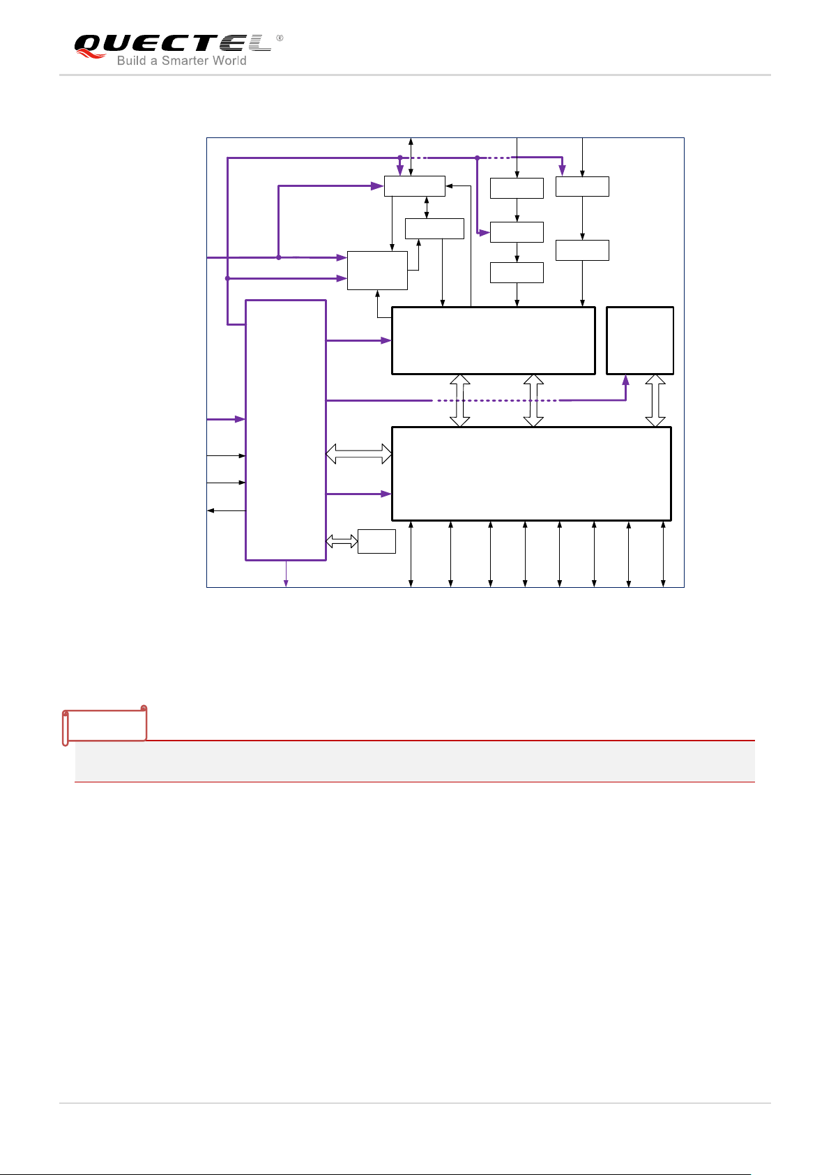
2.3. Functional Diagram
The following figure shows a block diagram of EG91 and illustrates the major functional parts.
Power management
Baseband
DDR+NAND flas h
Radio frequency
Peripheral interfaces
EG91_Hardware_Design 15 / 93
Page 17
LTE Standard Module Series
Baseband
PMIC
Transceiver
NAND
DDR2
SDRAM
PA
PAM
Switch
ANT_MAIN ANT_DIV
VBAT_BB
VBAT_RF
PWRKEY
VDD_EXT
USB PCM UARTI2C
RESET_N
19.2M
XO
STATUS
GPIOs
Control
IQ Control
Duplexer
SAW
Tx
PRx DRx
(U)SIM2
SPI
(U)SIM1
SAW
LNA
ANT_GNSS
1)
SAW
GPS
NOTE
EG91 Hardware Design
Figure 1: Functional Diagram
1)
GNSS antenna interface is only supported on EG91-NA/-NS/-VX/-EX.
2.4. Evaluation Board
Quectel provides a complete set of evaluation tools to facilitate the use and testing of EG91 module. The
evaluation tool kit includes the evaluation board (UMTS<E EVB), USB data cable, earphone, antenna
and other peripherals.
EG91_Hardware_Design 16 / 93
Page 18

LTE Standard Module Series
EG91 Hardware Design
3 Applicat i on Interfaces
3.1. General Description
EG91 is equipped with 62-pin 1.1mm pitch SMT pads plus 44-pin ground/reserved pads that can be
connected to customers’ cellular application platforms. Sub-interfaces included in these pads are
described in detail in the following chapters:
Power supply
(U)SIM interfaces
USB interface
UART interfaces
PCM and I2C interfaces
SPI interface
Status indication
USB_BOOT interface
EG91_Hardware_Design 17 / 93
Page 19
EG91 Hardware Design
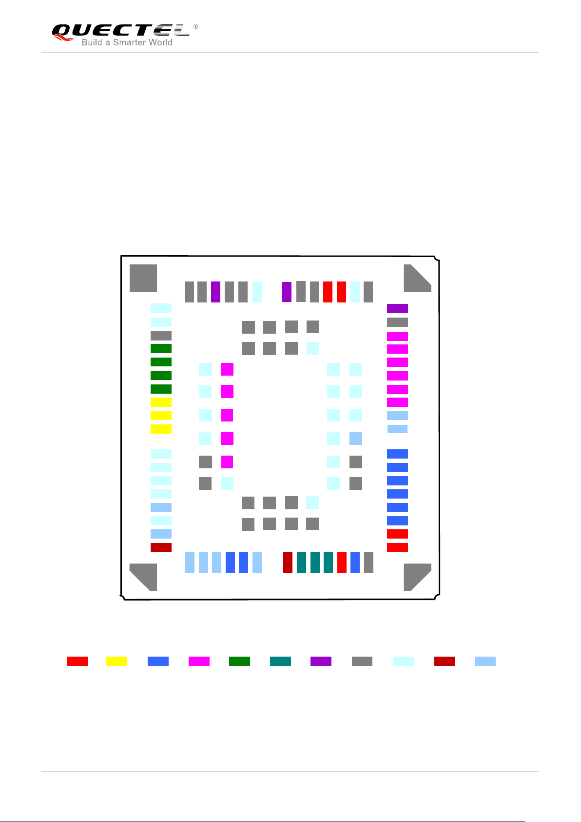
NC
PCM_SYNC
PCM_CLK
PCM_DIN
PCM_DOUT
NC
NC
PWRKEY
1)
NC
RES ET_N
RES ERVED
1
2
3
4
5
6
7
11
12
13
14
15
16
17
18
50
51
52
53
54
55
58
59
60
61
62
USB_DM
AP_READY
STATUS
NETLIGHT
DBG_RXD
DBG_TXD
ADC0
RES ERVED
SPI_CLK
SPI_MOSI
SPI_MISO
VDD_EXT
DTR
GND
USIM1_CLK
USIM1_DATA
USIM1_RST
USIM1_VDD
RI
DCD
CTS
TXD
RXD
VBAT_BB
VBAT_BB
USIM_GND
GND
31
30
29
28
27
26
23
22
21
20
19
10
9
USB_DP
USB_VBUS
NC
GND
NC
NC
RTS
I2C_SCL
I2C_SDA
8
49
48
47
46
45
44
43
40
41
42
39
38
37
36
35
34
33
32
24
57
56
GND
GND
ANT_MAIN
GND
GND
NC
VBAT_RF
VBAT_RF
GND
GND
NC
GND
USIM1_PRESENCE
63
64
65
66
67
68
83
84
85
86
87
88
98
97
96
95
94
93
78
77
76
75
74
73
91 92
89 90
71
72
69
70
80 79
82
81
100
99
102 101
POWER USB UART
(U)SIM
OTHERS
GND
NC
PCM
ANT
25
USIM2_PRESENCE
USIM2_CLK
USIM2_RST
USIM2_DATA
USIM2_VDD
SPI
USB_BOOT
103
104
105
106
ANT_DIV (EG91-NA/-NS/-VX/-EX)
ANT_GNSS (EG91-NA/-NS/-VX/-EX)
RES ERVED
RES ERVED (Pin 49 on EG91-E)
ANT_DIV (EG91-E)
3.2. Pin Assignment
The following figure shows the pin assi gnment of EG91 module.
LTE Standard Module Series
EG91_Hardware_Design 18 / 93
Figure 2: Pin Assignment (Top View)
Page 20
LTE Standard Module Series
Table 4
DC
Characteristics
NOTES
EG91 Hardware Design
1. 1) PWRKEY output volt age is 0.8V because of the diode drop in the Qualcomm chipset.
2. Keep all RESERVED pins and unused pins unco nnected.
3. GND pads should be connect ed to ground in the design.
4. Definition of pin 49 and 56 are different among EG91-E/-NS/-VX/-EX and EG91-NA. For more
details, please refer to
.
3.3. Pin Description
The following tables show the pin definition and description of EG91.
Table 3: IO Parameters Defi ni t ion
Type Description
AI Analog input
AO Analog output
DI Di g ital input
DO Digita l output
IO Bidirectional
OD Open drain
PI Power input
PO Power output
Table 4: Pin Description
Power Supply
Pin Name Pin No. I/O Description
VBAT_BB 32, 33 PI
EG91_Hardware_Design 19 / 93
Power supply for
module’s baseban d
part
Vmax=4.3V
Vmin=3.3V
Vnorm=3.8V
Comment
It must be able to
provide sufficient
current up to 0.8A.
Page 21
LTE Standard Module Series
3, 31, 48,
The output voltage is
status
open.
Vnorm=5.0V
open.
EG91 Hardware Design
It must be able to
provide sufficient
current up to 1.8A in a
burst transmission.
VBAT_RF 52, 53 PI
Power supply for
module’s RF part
Vmax=4.3V
Vmin=3.3V
Vnorm=3.8V
Power supply for
VDD_EXT 29 PO
Provide 1.8V for
external circuit
Vnorm=1.8V
I
max=50mA
O
external GPIO’s pu ll u p
circuits.
If unused, keep it open.
50, 54, 55,
58, 59, 61,
GND
62, 67~74,
Ground
79~82,
89~91,
100~106
Turn-on/off
Pin Name Pin No. I/O Description DC Characterist i cs Comment
V
max=2.1V
IH
V
min=1.3V
IH
V
max=0.5V
IL
0.8V because of the
diode drop in the
Qualcomm chipset.
PWRKEY 15 DI
Turn on/off the
module
Pull-up to 1.8V
RESET_N 17 DI
Reset signal of the
module
V
max=2.1V
IH
V
min=1.3V
IH
V
max=0.5V
IL
internally.
Active low.
If unused, keep it
open.
Status Indication
Pin Name Pin No. I/O Description DC Characterist i cs Comment
1.8V power domain.
If unused, keep it
1.8V power domain.
If unused, keep it
open.
STATUS 20 DO
NETLIGHT 21 DO
Indicate the
module’s operating
Indicate the
module’s network
activity status
VOHmin=1.35V
V
max=0.45V
OL
V
min=1.35V
OH
V
max=0.45V
OL
USB Interface
Pin Name Pin No. I/O Description DC Characterist i cs Comment
USB_VBUS 8 PI
EG91_Hardware_Design 20 / 93
USB connection
detection
Vmax=5.25V
Vmin=3.0V
Typical: 5.0V
If unused, keep it
Page 22

LTE Standard Module Series
specification.
connector.
IOmax=50mA
VOHmin=2.55V
EG91 Hardware Design
Compliant with USB
2.0 standard
Compliant with USB
2.0 standard
specification.
Require differenti al
impedance of 90Ω.
Require differenti al
impedance of 90Ω.
USB_DP 9 IO
USB_DM 10 IO
USB diffe rential
data bus (+)
USB diffe rential
data bus (-)
(U)SIM Interfaces
Pin Name Pin No. I/O Description DC Char acteristics Comment
Connect to ground of
(U)SIM card
USIM_GND 47
Specified ground for
(U)SIM card
For 1.8V (U)SIM:
Vmax=1.9V
Vmin=1.7V
USIM1_VDD 43 PO
Power supply for
(U)SIM card
For 3.0V (U)SIM:
Vmax=3.05V
Either 1.8V or 3.0V is
supported by the
module automatically.
Vmin=2.7V
USIM1_DATA 45 IO
USIM1_CLK 46 DO
Data signal of
(U)SIM card
Clock signal of
(U)SIM card
For 1.8V (U)SIM:
V
max=0.6V
IL
V
min=1.2V
IH
V
max=0.45V
OL
V
min=1.35V
OH
For 3.0V (U)SIM:
max=1.0V
V
IL
V
min=1.95V
IH
V
max=0.45V
OL
V
min=2.55V
OH
For 1.8V (U)SIM:
V
max=0.45V
OL
V
min=1.35V
OH
For 3.0V (U)SIM:
max=0.45V
V
OL
EG91_Hardware_Design 21 / 93
Page 23

EG91 Hardware Design
USIM1_RST 44 DO
USIM1_
PRESENCE
42 DI
USIM2_VDD 87 PO
USIM2_DATA 86 IO
USIM2_CLK 84 DO
USIM2_RST 85 DO
Reset signal of
(U)SIM card
(U)SIM card
insertion detection
Power supply for
(U)SIM card
Data signal of
(U)SIM card
Clock signal of
(U)SIM card
Reset signal of
(U)SIM card
LTE Standard Module Series
For 1.8V (U)SIM:
V
max=0.45V
OL
V
min=1.35V
OH
For 3.0V (U)SIM:
max=0.45V
V
OL
V
min=2.55V
OH
V
min=-0.3V
IL
V
max=0.6V
IL
V
min=1.2V
IH
V
max=2.0V
IH
For 1.8V (U)SIM:
Vmax=1.9V
Vmin=1.7V
For 3.0V (U)SIM:
Vmax=3.05V
Vmin=2.7V
I
max=50mA
O
For 1.8V (U)SIM:
V
max=0.6V
IL
V
min=1.2V
IH
V
max=0.45V
OL
V
min=1.35V
OH
For 3.0V (U)SIM:
max=1.0V
V
IL
V
min=1.95V
IH
V
max=0.45V
OL
V
min=2.55V
OH
For 1.8V (U)SIM:
V
max=0.45V
OL
V
min=1.35V
OH
For 3.0V (U)SIM:
max=0.45V
V
OL
V
min=2.55V
OH
For 1.8V (U)SIM:
V
max=0.45V
OL
V
min=1.35V
OH
For 3.0V (U)SIM:
max=0.45V
V
OL
1.8V power domain.
If unused, keep it
open.
Either 1.8V or 3.0V is
supported by the
module automatically.
EG91_Hardware_Design 22 / 93
Page 24
LTE Standard Module Series
open.
VIHmax=2.0V
EG91 Hardware Design
VOHmin=2.55V
V
min=-0.3V
USIM2_
PRESENCE
83 DI
(U)SIM card
insertion detection
IL
V
max=0.6V
IL
V
min=1.2V
IH
V
max=2.0V
IH
1.8V power domain.
If unused, keep it
open.
Main UART Interface
Pin Name Pin No. I/O Description DC Characterist i cs Comment
RI 39 DO Ring indicator
DCD 38 DO
Data carrier
detection
CTS 36 DO Clear to send
RTS 37 DI Request t o send
DTR 30 DI
Data terminal ready.
Sleep mode control.
V
max=0.45V
OL
V
min=1.35V
OH
V
max=0.45V
OL
V
min=1.35V
OH
V
max=0.45V
OL
V
min=1.35V
OH
V
min=-0.3V
IL
V
max=0.6V
IL
V
min=1.2V
IH
V
min=-0.3V
IL
V
max=0.6V
IL
V
min=1.2V
IH
V
max=2.0V
IH
1.8V power domain.
If unused, keep it
open.
1.8V power domain.
If unused, keep it
open.
1.8V power domain.
If unused, keep it
1.8V power domain.
If unused, keep it
open.
1.8V power domain.
Pull-up by default.
Low level wakes up
the module.
If unused, keep it
open.
TXD 35 DO Transmit data
RXD 34 DI Receive data
Debug UART Int er face
Pin Name Pin No. I/O Description DC Characterist i cs Comment
DBG_TXD 23 DO Transmit data
EG91_Hardware_Design 23 / 93
V
max=0.45V
OL
V
min=1.35V
OH
V
min=-0.3V
IL
V
max=0.6V
IL
V
min=1.2V
IH
V
max=2.0V
IH
V
max=0.45V
OL
V
min=1.35V
OH
1.8V power domain.
If unused, keep it
open.
1.8V power domain.
If unused, keep it
open.
1.8V power domain.
If unused, keep it
Page 25
LTE Standard Module Series
VIHmax=2.0V
VIHmax=2.0V
open.
open.
open.
EG91 Hardware Design
open.
V
min=-0.3V
DBG_RXD 22 DI Receive data
IL
V
max=0.6V
IL
V
min=1.2V
IH
1.8V power domain.
If unused, keep it
open.
PCM Interface
Pin Name Pin No. I/O Description DC Characterist i cs Comment
V
min=-0.3V
PCM_DIN 6 DI PCM data input
IL
V
max=0.6V
IL
V
min=1.2V
IH
1.8V power domain.
If unused, keep it
open.
PCM_
DOUT
7 DO PCM data output
PCM data frame
PCM_SYNC 5 IO
synchronization
signal
PCM_CLK 4 IO PCM clock
I2C Interface
V
max=0.45V
OL
V
min=1.35V
OH
max=0.45V
V
OL
V
min=1.35V
OH
V
min=-0.3V
IL
V
max=0.6V
IL
V
min=1.2V
IH
V
max=2.0V
IH
max=0.45V
V
OL
V
min=1.35V
OH
V
min=-0.3V
IL
V
max=0.6V
IL
V
min=1.2V
IH
V
max=2.0V
IH
1.8V power domain.
If unused, keep it
open.
1.8V power domain.
In master mode, it is
an output signal. In
slave mode, it is an
input signal.
If unused, keep it
1.8V power domain.
In master mode, it is
an output signal. In
slave mode, it is an
input signal.
If unused, keep it
Pin Name Pin No. I/O Description DC Characteristics Comment
I2C_SCL 40 OD
I2C_SDA 41 OD
EG91_Hardware_Design 24 / 93
I2C serial clock.
Used for external
codec
I2C serial data.
Used for external
codec
An external pull-up
resistor is required.
1.8V only.
If unused, keep it
An external pull-up
resistor is required.
1.8V only.
If unused, keep it
open.
Page 26
LTE Standard Module Series
open.
56
50Ω impedance.
open.
EG91 Hardware Design
ADC Interface
Pin Name Pin No. I/O Description DC Characteristics Comment
ADC0 24 AI
General purpose
analog to digital
converter
Volta ge r ange:
0.3V to VBAT_BB
If unused, keep it
open.
SPI Interface
Pin Name Pin No. I/O Description DC Characteristics Comment
1.8V power domain.
If unused, keep it
1.8V power domain.
If unused, keep it
open.
1.8V power domain.
If unused, keep it
open.
SPI_CLK 26 DO
SPI_MOSI 27 DO
SPI_MISO 28 DI
Clock signal of SPI
interface
Master output slave
input of SPI
interface
Master input slave
output of SPI
interface
V
max=0.45V
OL
V
min=1.35V
OH
V
max=0.45V
OL
V
min=1.35V
OH
V
min=-0.3V
IL
V
max=0.6V
IL
V
min=1.2V
IH
V
max=2.0V
IH
RF Interfaces
Pin Name Pin No. I/O Description DC Characteristics Comment
50Ω impedance.
If unused, keep it
open.
The pin is defined as
ANT_DIV on
ANT_GNSS
49
(EG91NA/-NS/
-VX/-EX)
AI GNSS antenna pad
EG91-E.
49
ANT_DIV
(EG91E)
(EG91NA/-NS/
AI
Receive diversity
antenna pad
50Ω impedance.
If unused, keep it
open.
The pin is reserved
on EG91-E.
-VX/-EX)
ANT_MAIN 60 IO Main antenna pad
If unused, keep it
Other Pins
Pin Name Pin No. I/O Description DC Characteristics Comment
EG91_Hardware_Design 25 / 93
Page 27
LTE Standard Module Series
to send and receive data.
decided by network setting and data transfer rate.
command can set the module to a minimum functionality mode without
enter into
NOTE
EG91 Hardware Design
V
min=-0.3V
AP_READY 19 DI
USB_BOOT 75 DI
Application
processor sleep
state detection
Force the module to
emergency
download mode
IL
V
max=0.6V
IL
V
min=1.2V
IH
V
max=2.0V
IH
VILmin=-0.3V
V
max=0.6V
IL
V
min=1.2V
IH
V
max=2.0V
IH
1.8V power domain.
If unused, keep it
open.
1.8V power domain.
It is recommended to
reserve the test
points.
RESERVED Pins
Pin Name Pin No. I/O Description DC Characteristics Comment
1,2, 11~14,
NC
16, 51,
57, 63~66,
76~78,
NC
Keep these pins
unconnected.
88, 92~99
Keep these pins
RESERVED 18, 25, 49 Reserved
unconnected.
Pin 49 is only
reserved on EG91-E.
Keep all RESERVED pins and unused pins unconn ect ed.
3.4. Operating Modes
The table below briefly su m m ar iz es the various operating modes re ferr ed in the following chapters.
Table 5: Overview of Operating Modes
Mode Details
Idle
Software is active. The mo dule has registered on network, and it is ready
Normal
Operation
Talk/Data
Minimum
Functionality
EG91_Hardware_Design 26 / 93
AT+CFUN
removing the power supp ly. In this case, bot h RF funct ion and (U)SIM card will be invalid.
Network connection is ongoing. In this mode, the power consumption is
Page 28
Mode
In this mode, the current consu m ption of the module will be reduced to the minimal level.
TCP/UDP data from the network normally.
RXD
TXD
RI
DTR
AP_READY
TXD
RXD
EINT
GPIO
GPIO
Module
Host
GND
GND
LTE Standard Module Series
EG91 Hardware Design
Airplane
Mode
Sleep Mode
Power Down
Mode
AT+CFUN command or W_DISABLE# pin can set the module to enter into airplane mode.
In this case, RF function will be invalid.
During this mode, the module can still receive paging message, SMS, voice call and
In this mode, the power management unit shuts down the power supply. Software is not
active. The serial interface is not accessible. Operating voltage (connected to VBAT_RF
and VBAT_BB) remains a ppl ied.
3.5. Power Saving
3.5.1. Sleep Mode
EG91 is able to reduce its current consumption to a mini mu m v alue during the sleep mode. The following
sub-chapters describe the pow er saving procedures of EG91 module.
3.5.1.1. UART Application
If the host communicates with the module via UART interface, the following preconditions can let the
module enter into sleep mode.
Execute AT+QSCLK=1 command to enable sleep mode.
Drive DTR to high level.
The following figure shows the connection between the module and the host.
Figure 3: Sleep Mode Application via UART
Driving the host DTR to low level will wake up the m odule.
EG91_Hardware_Design 27 / 93
Page 29
LTE Standard Module Series
USB_VBUS
USB_DP
USB_DM
AP_READY
VDD
USB_DP
USB_DM
GPIO
Module
Host
GND
GND
NOTE
EG91 Hardware Design
When EG91 has a URC to report, RI signal will wake up the host. Please refer to Chapter 3.17 for
details about RI behavior.
AP_READY will detec t t he sleep state of host (can be configured to high level or low l evel detection).
Please refer to AT+QCFG="apready"* command for details.
“*” means under develop me nt .
3.5.1.2. USB Application with USB Rem ot e Wake up Fu n cti on
If the ho st support s USB s uspend/resu me and r emote w akeup functions, the following three preconditions
must be met to let the module enter into sleep mod e.
Execute AT+QSCLK=1 command to enable sleep mode.
Ensure the DTR is held at high level or keep it open.
The host’s USB bus, which is connected with the m odule’s USB interface, enters into su spend state.
The following figure shows the connection between the module and the host.
Figure 4: Sleep Mode Appli cat i on with USB Remote Wakeup
Sending data to EG91 through USB will wake up the module.
When EG91 has a URC to report, the module will send remote wakeup signals via USB bus so as to
wake up the host.
3.5.1.3. USB Application with USB Suspend/Re sum e and RI Function
If the host supports USB suspend/resume, but does not support remote wakeup function, the RI signal is
needed to wake up the host.
There are three preconditions to let the module enter into the sleep mod e.
EG91_Hardware_Design 28 / 93
Page 30

LTE Standard Module Series
USB_VBUS
USB_DP
USB_DM
AP_READY
VDD
USB
_
DP
USB_DM
GPIO
Module Host
GND
GND
RI
EINT
USB_VBUS
USB_DP
USB_DM
AP_READY
VDD
USB_DP
USB_DM
GPIO
Module Host
RI
EINT
Power
Switch
GPIO
GND
GND
EG91 Hardware Design
Execute AT+QSCLK=1 command to enable sleep mode.
Ensure the DTR is held at high level or keep it open.
The host’s USB bus, which is connecte d with the module’s US B interface, enters into suspended state.
The following figure shows the connection between the module and the host.
Figure 5: Sleep Mode Appl icat ion wi th RI
Sending data to EG91 through USB will wake up the module.
When EG91 has a URC to report, RI signal will wake up the host.
3.5.1.4. USB Application witho ut USB Su spe n d Function
If the host does not support USB suspend function, USB_VBUS should be disconn ect ed with an external
control circuit to let the mo dul e enter into sleep mode.
Execute AT+QSCLK=1 command to enable sleep mode.
Ensure the DTR is held at high level or keep it open.
Disconnect USB_VBUS.
The following figure shows the connection between the module and the host.
EG91_Hardware_Design 29 / 93
Figure 6: Sleep Mode Application wit hout Suspend Func t ion
Page 31

LTE Standard Module Series
document [1]
2. The execution of AT+CFUN command w i ll n ot affect GNSS function.
NOTE
NOTES
EG91 Hardware Design
Switching on the power switch to supply power t o U SB _VBUS will wake up the module.
Please pay attention to the level match shown in dotted line between the module and the host. Please
refer to
3.5.2. Airplane Mode
When the module enters into airplane mode, the RF function does not work, and all AT commands
correlative with RF functio n will be inaccessible. This mode can be set via the followin g ways.
Hardware:
The W_DISABLE# pin is pulled up by default. Driving it to low level will let the module enter into airplane
mode.
Software:
for more details about EG91 power m anagement application.
AT+CFUN command provides the choice of the functionality level through setti ng <fun> into 0, 1 or 4.
AT+CFUN=0: Minimum functionality mode. Both (U)SIM and RF functions are disa bled.
AT+CFUN=1: Full functionality mode (by default).
AT+CFUN=4: Airplane mode. RF fu nc t i on is disabled.
1. Airplane mode control via W_DISABLE# is disabled in firmware by default. It can be enabled by
AT+QCFG="airplanecontrol" command and this command is under development.
3.6. Power Supply
3.6.1. Pow er Supply Pins
EG91 provid es four VBA T pins d edicated to connect with an external power supply. There are two separate
voltage domains for VBAT.
Two VBAT_RF pins for module’s RF part.
Two VBAT_BB pins for module’s baseband part.
The following table shows the details of VBAT pins and ground pins.
EG91_Hardware_Design 30 / 93
Page 32

LTE Standard Module Series
RF part.
VBAT
Min.3.3V
Ripple
Drop
Burst
Transmission
Burst
Transmission
EG91 Hardware Design
Table 6: Pin Definition of VBAT and GND
Pin Name Pin No. Description Min. Typ. Max. Unit
VBAT_RF 52, 53
VBAT_BB 32, 33
Power supply for module’s
Power supply for module’s
baseband part.
3.3 3.8 4.3 V
3.3 3.8 4.3 V
3, 31, 48, 50,
54, 55, 58, 59,
GND
61, 62, 67~74,
Ground - 0 - V
79~82, 89~91,
100~106
3.6.2. Decrease Voltage Drop
The power supply range of the module is from 3.3V to 4.3V. Please make sure that the input voltage will
never drop below 3.3V. The following figure shows the voltage drop during burst transmission in 2G
network. The voltage drop will be less in 3G and 4G networks.
Figure 7: Power Supply Limits during B ur s t Transmission
To decrease voltage drop, a bypass capacitor of ab out 100µF with low ESR (ESR=0.7Ω) should be used,
and a multi-layer ceramic chip (MLCC) capacitor array should also be reserved due to its ultra-low ESR. It
is recommended to use three ceramic capacitors ( 100nF, 33pF, 10pF) for composing th e MLCC arr ay, and
place these capacitors close to VBAT_BB/VBAT_RF pins. The main power supply from an external
application has to be a single voltage source and can be expanded to two sub paths with star structure.
The width of VBAT_BB trace should be no less than 1mm, and the width of VBAT_RF trace should be no
less than 2mm. In principle, the longer the VBAT trace is, the wider it will be.
In addition, in order to avoid the damage caused by electric surge and ESD, it is suggested that a TVS
diode with low reverse stand-off voltage V
current I
should be used. The following figure shows the star structure of the power sup ply.
PP
EG91_Hardware_Design 31 / 93
, low clamping voltage VC and high reverse peak pulse
RWM
Page 33

EG91 Hardware Design
Module
VBAT_RF
VBAT_BB
VBAT
C1
100uF
C6
100nFC733pFC810pF
+
+
C2
100nF
C5
100uF
C3
33pF
C4
10pF
D1
WS4.5D3HV
DC_IN
MIC
29302
WU
IN
OUT
EN
GND
ADJ
2 4
1
3
5
VBAT
100nF
470uF
100nF
100K
47K
470uF
470R
51K
1%
1%
4.7K
47K
VBAT_EN
Figure 8: Star Structure of the Power Supply
3.6.3. Refe r ence Design for Power Supply
LTE Standard Module Series
Power design for the module is very important, as the performance of the module largely depends on the
power source. The power supp ly should be able to prov ide s ufficient cur rent up to 2A at least. I f the voltage
drop between the input and output is not too high, it is suggested that an LDO should be used to supply
power for the module. If there is a big voltage difference between the in put source and the desired output
(VBAT), a buck converter is preferred to be used as the power supply.
The following figure show s a referenc e design for + 5V input pow er sour ce. The typical output of the power
supply is about 3.8V and t he maximum load current is 3A.
Figure 9: Refer ence Circuit of Power Supply
3.6.4. Monitor the Power Supply
AT+CBC command can be used to monitor t he VBAT_BB voltage value. For more details, please refer to
document [2].
EG91_Hardware_Design 32 / 93
Page 34

LTE Standard Module Series
VIHmax=2.1V
VILmax=0.5V
The output voltage is 0.8V
the Qualcomm chipset.
Turn on pulse
PWRKEY
4
.
7K
47
K
≥
5
00
ms
10nF
EG91 Hardware Design
3.7. Power-on/off Scenarios
3.7.1. Turn on Module Using the PWRKEY
The following table shows the pin definition of P WR KEY.
Table 7: Pin Definition of PWRKEY
Pin Name Pin No. Description DC Characteristics Comment
PWRKEY 15 Turn on/off the module
VIHmin=1.3V
because of the diode drop in
When EG91 is in power down mode, it can be turned on to normal mode by driving the PWRKEY pin to a
low level for at least 500ms. It is recommended to use an open drain/collector driver to control the PWRKEY.
After STATUS pin outputting a high level, PWRKEY pin can be released. A simple reference circuit is
illustrated in the following figure.
Another way to control the PWRKEY is using a button directly. When pressing the key, electrostatic strike
may generate from the finger. Therefore, a TVS component is in dispensable to be p laced nearby the button
for ESD protection. A reference circuit is shown in the following figure.
EG91_Hardware_Design 33 / 93
Figure 10: Turn on the Module Using Driving Circuit
Page 35

EG91 Hardware Design
PWRKEY
S
1
Close to S1
TVS
V
IL
≤0.5V
V
H
=0.8V
VBAT
PWRKEY
≥500ms
RESET_N
STATUS
(DO)
Inactive
Active
UART
NOTE
Inactive
Active
USB
≥2.5s
≥12s
≥13s
VDD_EXT
BOOT_CONFIG &
USB_BOOT Pins
≥100ms, afte r th is ti m e, the BOOT_CONFIG &
USB_BOOT pins can be set high level by
external circuit.
About 100ms
Figure 11: Turn on the Module Using Button
The power-on scenario is il lust r at ed in the following figure.
LTE Standard Module Series
Figure 12: Power-on Scenario
EG91_Hardware_Design 34 / 93
Page 36

LTE Standard Module Series
VBAT
PWRKEY
≥ 30s
≥
650ms
RUNNING
Power-down procedure
OFF
Module
Status
STATUS
NOTES
EG91 Hardware Design
1. Please make sure that VBAT is stable before pulling down PWRKEY pin. The time between them
is no less than 30ms.
2. PWRKEY can be pulled down directly to GND with a recommended 10K resistor if module needs
to be powered on automatica lly and shutdown is not needed.
3.7.2. Turn off Module
Either of the following methods can be used to t ur n off the module:
Normal power-off procedu re: T urn off the modu le using the PWRKEY pin.
Normal power-off procedu re: T urn off the modu le using AT+QPOWD command.
3.7.2.1. Turn off Module Usin g t he PWRKEY Pin
Driving the PWRKEY pin to a low level voltage for at least 650ms, the module will execute power-off
procedure after the PWRKEY is released. The power-off scenar io is illustrate d in the fol lowing figur e.
Figure 13: Power-off Scenario
3.7.2.2. Turn off Module Usin g AT Command
It is also a safe way to use AT+QPOWD command to turn off the module, which is sim ilar to turning o ff th e
module via PWRKEY pin.
Please refer to docum ent [2] for details about the AT+QPOWD command.
EG91_Hardware_Design 35 / 93
Page 37

LTE Standard Module Series
VILmax=0.5V
Reset pulse
RESET_N
4.7K
47K
150ms~460ms
NOTES
EG91 Hardware Design
1. In order to avoid damaging internal flash, please do not switch off the power supply when the
module works normally. Only after the module is shut down by PWRKEY or AT command, the
power supply can be cut off.
2. When turning off module with AT command, please k eep PWRKEY at high level after the ex ecution
of power-off comma nd. Otherwise the module will be t ur ned on again after successful turn-off.
3.8. Reset the Module
The RESET_N pin can be used to reset the module. The module can be reset by driving RESET_N to a
low level voltage for 150ms~460ms.
Table 8: Pin Definition of RESET_N
Pin Name Pin No. Description DC Characteristics Comment
max=2.1V
V
IH
RESET_N 17 Reset the module
V
min=1.3V
IH
The recommended circu it is simi lar to the P WRKEY control circ uit. An ope n drain/co llector dr iver or button
can be used to control the RESE T_N.
EG91_Hardware_Design 36 / 93
Figure 14: Reference Circuit of RESET_ N by Using Driving Circuit
Page 38

EG91 Hardware Design
RESET
_
N
S
2
Close to S2
TVS
VIL ≤ 0.5V
V
IH
≥ 1.3V
VBAT
≥ 150ms
Resetting
Module
Status
Running
RESET_N
Restart
≤ 460ms
NOTES
Figure 15: Reference Circuit of RESET_N by Using Button
The reset scenario is illustrated in the following figure.
LTE Standard Module Series
Figure 16: Reset Scenario
1. Use RESET_N only when turning off the module by AT+QPOWD command and PWRKEY pin
failed.
2. Ensure that there is no large capacitance on PWRKEY and RESET_N pins.
3.9. (U)SIM Interfaces
EG91 provides two (U)SIM i nterfaces, and only one (U)SIM card can work at a time. The (U)SIM1 and
(U)SIM2 cards can be switched by AT+QDSIM* command. For more details, please refer to document
[2].
The (U)SIM interfaces circuitry meet ETSI and IMT-2 000 requ ireme nts. Both 1.8V and 3. 0V (U)SIM cards
are supported.
EG91_Hardware_Design 37 / 93
Page 39

LTE Standard Module Series
EG91 Hardware Design
Table 9: Pin Definition of (U)SIM Interfaces
Pin Name Pin No. I/O Description Comment
Either 1.8V or 3.0V is
USIM1_VDD 43 PO Power supply for (U)SIM1 card
supported by the module
automatically.
USIM1_DATA 45 IO Data signal of (U)SIM1 card
USIM1_CLK 46 DO Clock signal of (U)SIM1 card
USIM1_RST 44 DO Reset signal of (U)SIM1 card
USIM1_
PRESENCE
42 DI (U)SIM1 card insertion detection
USIM_GND 47 Specified gro und for (U)SIM card
Either 1.8V or 3.0V is
USIM2_VDD 87 PO Power supply for (U)SIM2 card
supported by the module
automatically.
USIM2_DATA 86 IO Data signal of (U)SIM2 card
USIM2_CLK 84 DO Clock signal of (U)SIM2 card
USIM2_RST 85 DO Reset signal of (U)SIM2 card
USIM2_
PRESENCE
83 DI (U)SIM2 card insertion detection
EG91 supports (U)SIM card hot-plug via USIM_PRESENCE (USIM1_PRESENCE/USIM2_PRESENCE)
pin. The function supports low level and high level detection, and is disabled by default. Please refer to
document [2] about AT+QSIMDET command for details.
The following figure shows a reference design for (U)SIM interface with an 8-pin (U)SIM card connector.
EG91_Hardware_Design 38 / 93
Page 40

LTE Standard Module Series
Module
USIM
_
VDD
USIM
_GND
USIM
_
RST
USIM
_
CLK
USIM
_
DATA
USIM
_
PRESENCE
0
R
0
R
0
R
VDD
_
EXT
51K
100nF (U)SIM Card Connector
GND
GND
33pF
33pF
33pF
VCC
RST
CLK
IO
VPP
GND
GND
U
SIM
1
_
VDD
15
K
Module
USIM_
VDD
USIM_GND
USIM_RST
USIM_CLK
USIM_DATA
0R
0R
0
R
100nF
(U)SIM Card Connector
GND
33pF
33pF 33pF
VCC
RST
CLK IO
VPP
GND
GND
15K
USIM1_VDD
EG91 Hardware Design
Figure 17: Reference Circui t of (U)SIM Interface with an 8-Pin (U)SIM Card Connector
If (U)SIM card detect ion function is not n eeded, please keep USIM_PRESE NCE unconnected. A reference
circuit of (U)SIM interface with a 6-pin (U)SIM card connector is illustrated in the following figure.
Figure 18: Reference Circui t of (U)SI M Interface with a 6-Pin (U)SIM Card Connector
In order to enhance the reliability and availability of the (U)SIM card in customers’ applications, please
follow the criteria below in t he (U)SIM circuit design:
Keep placement of (U)SIM card connector to the module as close as possible. Keep the trace length
Keep (U)SIM card signals away from RF and VBAT traces.
Assure the ground trace between the module and the (U)SIM card connector short and wide. Keep
as less than 200mm as possible.
EG91_Hardware_Design 39 / 93
Page 41

LTE Standard Module Series
impedance of 90Ω.
NOTE
EG91 Hardware Design
the trace width of ground and USIM_V DD no less than 0.5 mm to mainta in the same electr ic potentia l.
Make sure the bypass cap ac itor bet ween USIM_VDD and U SIM _GND less than 1uF, and place it as
close to (U)SIM card c onnector as pos sible. If the ground is complete on customers’ PCB, USIM_GND
can be connected to PCB ground directly.
T o avoid cross-tal k between USIM_DA T A and USIM_CLK, keep them away from each other and shield
them with surrounded ground.
In order to offer good ESD protection, it is recommended to add a TVS diode array whose parasitic
capacitance should not be more than 15pF. The 0Ω resistors should be added in series between the
module and the (U)SIM card to facilitate debugging. The 33pF capacitors are used for filtering
interference of EGSM900. Please note that the (U)SIM per ipheral circuit should be close to t he (U)SIM
card connector.
The pull-up resistor on USIM_DATA line can improve anti-jamming capability when long layout trace
and sensitive occasion are applied, and should be placed close to t he (U)SIM card connector.
“*” means under develop me nt .
3.10. USB Interface
EG91 contains one integrated Universal Serial Bus (USB) interface which complies with the USB 2.0
specification and supports high-speed (480Mbps) and full-speed (12Mbps) modes. The USB interface is
used for AT command communication, data transmission, GNSS NMEA sentences output, software
debugging, firmware upgrade and voice over USB*. The following table shows the pin definition of USB
interface.
Table 10: Pin Definition of USB Interface
Pin Name Pin No. I/O Description Comment
USB_DP 9 IO USB differential data bus (+)
Require differenti al
USB_DM 10 IO USB differential data bus (-)
USB_VBUS 8 PI USB connection detection Typical: 5.0V
GND 3 Ground
For more details about USB 2.0 spec i fi cat io ns , pl ease visit http://www.usb.org/home
EG91_Hardware_Design 40 / 93
Require differenti al
impedance of 90Ω.
.
Page 42

LTE Standard Module Series
USB_DP
USB_DM
GND
USB_DP
USB_DM
GND
L1
Close to Module
R3
R4
Test Points
ESD Array
NM_0R
NM_0R
Minimize these stubs
Module
MCU
USB_VBUS
VDD
NOTES
EG91 Hardware Design
The USB interface is recommended to be reserved for firmware upgrade in customers’ design. The
following figure shows a reference circuit of USB interfac e.
Figure 19: Reference Circuit of USB Interface
A common mode choke L1 is recommended to be added in series between the module and customer’s
MCU in order to suppress EMI spurious transmission. Meanwhile, the 0Ω resistors (R3 and R 4) sho uld b e
added in series between t he modul e and the t est poi nts so as to fac ilitate d ebugging, and t he res istors ar e
not mounted by default. In order to ensure the integrity of USB data line signal, L1/R3/R4 components
must be placed close to the module, and also these resistors should be placed close to each other. The
extra stubs of trace must be as s hort as possible.
The following principles should be complied with when design t he U SB interface, so as to meet USB 2.0
specification.
It is important to route the USB s ign al trace s as d if fe rentia l pairs w ith tot al gro undi ng. The i mped ance
of USB differential tr ace is 90Ω.
Do not route signal traces under crystals, oscillators, magnetic devices and RF signal traces. It is
important to route the USB differential traces in inner-layer with ground shielding on not only upper
and lower layers but also right and left sides.
Pay attention to the influence of junction capacitance of ESD protection components on USB data
lines. Typically, the capaci t ance value should be less than 2pF.
Keep the ESD protection components to the USB conne ctor as close as possible.
1. EG91 module ca n only be used as a slave device.
2. “*” means under development.
EG91_Hardware_Design 41 / 93
Page 43

LTE Standard Module Series
EG91 Hardware Design
3.11. UART Inter f a c e s
The module provides two UART interfaces: the main UART interface and the debug UART interface. The
following shows their features.
The main UART interface supports 9600bps, 19200bps, 38400bps, 57600bps, 115200bps,
230400bps, 460800bps, 921600bps and 3000000bps baud rates, and the default is 115200bps. It
supports RTS and CT S hardware flow control, and is used for AT command communicat ion only .
The debug UART int erface suppor ts 115200b ps baud rate. It is used for Linux console and log out put.
The following tables show the pin definition of the two UART interfaces.
Table 11: Pin Definition of Main UART Interfaces
Pin Name
Pin No. I/O Description Comment
RI 39 DO Ring indicator
DCD 38 DO Data carrier detection
CTS 36 DO Clear to send
RTS 37 DI Request to send
1.8V power domain
DTR 30 DI Sleep mode control
TXD 35 DO Transmit data
RXD 34 DI Receive data
Table 12: Pin Definition of Debu g UART Interface
Pin Name Pin No. I/O Description Comment
DBG_TXD 23 DO Transmit data 1.8V power domain
DBG_RXD 22 DI Receive data 1.8V power domain
The logic levels are described i n t he following table.
EG91_Hardware_Design 42 / 93
Page 44

LTE Standard Module Series
VCCA VCCB
OE
A1
A2
A3
A4
A5
A6
A7
A8
GND
B1
B2
B3
B4
B5
B6
B7
B8
VDD_EXT
RI
DCD
RTS
RXD
DTR
CTS
TXD
51K
51K
0.1uF
0.1uF
RI_MCU
DCD_MCU
RTS_MCU
RXD_MCU
DTR_MCU
CTS_MCU
TXD_MCU
VDD_MCU
Translator
EG91 Hardware Design
Table 13: Logic Levels of Digital I/O
Parameter Min. Max. Unit
VIL -0.3 0.6 V
VIH 1.2 2.0 V
VOL 0 0.45 V
VOH 1.35 1.8 V
The module provides 1.8V UART interfaces. A level translator should be u sed if customers’ appli cati o n i s
equipped with a 3.3V U AR T interface. A level translator TXS0108E P WR prov ided by Texas Instrument s is
recommended. The following figure shows a r ef er ence design.
Figure 20: Reference Circuit with Translator Chip
Please visit http://www.ti.com
for more information.
Another example with transistor translation circuit is shown as below. The circuit design of dotted line
section can refer to the circuit design of solid line section, in terms of both module input and output circuit
design. Please pay attention to the direction of conn ect ion.
EG91_Hardware_Design 43 / 93
Page 45

LTE Standard Module Series
MCU/ARM
TXD
RXD
VDD_EXT
10K
VCC_MCU
4.7K
10K
VDD_EXT
TXD
RXD
RTS
CTS
DTR
RI
RTS
CTS
GND
GPIO DCD
Module
GPIO
EINT
VDD_EXT
4.7K
GND
1nF
1nF
NOTE
EG91 Hardware Design
Figure 21: Reference Circuit with Transistor Circuit
Transistor circuit solut ion is not suitable for applications w it h high baud rates exceeding 460Kb ps.
3.12. PCM and I2C Interfaces
EG91 provides one Pulse Code Modulation (PCM) digital interface for audio design, which supports the
following modes and one I 2C interface:
Primary mode (short frame synchronization, works as both master and slave)
Auxiliary mode (long frame synchronization, works as master only)
In primary mode, the data is sampled on the falling edge of the PCM_CLK and transmitted on the rising
edge. The PCM_SYNC falling edge repres ents the MSB. In this mode, the PCM interface sup ports 256KHz,
512KHz, 1024KHz or 2048KHz PCM_CLK a t 8KHz PCM_SYNC, and also supports 4096KHz PCM_CLK
at 16KHz PCM_SYNC.
In auxiliary mode, the data is also sampled on the falling edge of the PCM_CLK and transmitted on the
rising edge. The PCM_SYNC rising edge represents the MSB. In this mode, the PCM interface operates
with a 256KHz, 512KHz, 1024KHz or 2048KHz PCM_CLK and an 8KHz, 50% duty cycle PCM_SYNC.
EG91 supports 16-bit linear data format. The follow ing figures s how the primary mode’ s timing r elationship
with 8KHz PCM_SYNC and 2048KHz PCM_CLK, as wel l as the auxiliary mode’s timing relationship with
8KHz PCM_SYNC and 256KHz PCM_CLK.
EG91_Hardware_Design 44 / 93
Page 46

LTE Standard Module Series
PCM_CLK
PCM_SYNC
PCM
_
DOUT
MSB
LSB
MSB
125
us
1
2
256255
PCM_DIN
MSB
LSBMSB
PCM_CLK
PCM_SYNC
PCM_DOUT
MSB
LSB
PCM
_DIN
125
us
MSB
1 2
3231
LSB
EG91 Hardware Design
Figure 22: Primary Mode Timing
Figure 23: Auxiliary Mode Timing
The following table shows the pin definition of PCM and I2C interfaces which can be applied on audio
codec design.
EG91_Hardware_Design 45 / 93
Page 47

LTE Standard Module Series
PCM_DIN
PCM_DOUT
PCM_SYNC
PCM_CLK
I2C_SCL
I2C_SDA
Module
1.8V
4.7K
4.7K
BCLK
LRCK
DAC
ADC
SCL
SDA
BIAS
MICBIAS
INP
INN
LOUTP
LOUTN
Codec
NOTES
EG91 Hardware Design
Table 14: Pin Definition of PCM and I2C Interfaces
Pin Name Pin No. I/O Description Comment
PCM_DIN 6 DI PCM data input 1.8V power domain
PCM_DOUT 7 DO PCM data output 1.8V power domain
PCM_SYNC 5 IO
PCM data frame
synchronization signal
1.8V power domain
PCM_CLK 4 IO PCM data bit clock 1.8V power domain
I2C_SCL 40 OD I2C serial clock Require an external pull-up to 1.8V
I2C_SDA 41 OD I2C serial data Require an external pull-up to 1.8V
Clock and mode can be configured by AT command, and the default configuration is master mode using
short frame synchronization format with 2048KHz PCM_CLK and 8KHz PCM_SYNC. Please refer to
document [2] about AT+QDAI command for details.
The following figure shows a reference design of PCM interface with exter nal c odec I C.
Figure 24: Refer ence Circuit of PC M Application with Audio Codec
1. It is recommended to reserve an RC (R=22Ω, C=22pF) circuit on the PCM lines, especially for
PCM_CLK.
2. EG91 works as a master device pertaining to I2 C interface.
EG91_Hardware_Design 46 / 93
Page 48

LTE Standard Module Series
SPI_MISO
SPI
_MOSI
SPI_CLK
Module
SPI_CLK
SPI_MOSI
SPI_MISO
Peripherals
host if customer’s application is equipped with a 3.3V processor or dev ic e interface.
NOTE
EG91 Hardware Design
3.13. SPI Interface
SPI interface of EG91 acts as the master only. It provides a duplex, synchronous and serial comm unication
link with the peripheral devices. It is dedicated to one-to-one connecti on, without chip select. Its operation
voltage is 1.8V with clock rates up to 50MHz.
The following table shows t he pin definition of SPI interface.
Table 15: Pin Definition of SPI Interface
Pin Name Pin No. I/O Description Comment
SPI_CLK 26 DO Clock signal of SPI interface 1.8V power domain
SPI_MOSI 27 DO
SPI_MISO 28 DI
Master output slave input of SPI
interface
Master input slave output of SPI
interface
1.8V power domain
1.8V power domain
The following figure shows a reference design of SPI interface with peripherals.
Figure 25: Reference Circuit of SPI Interface with Peripherals
The module provides 1.8 V SPI interface. A level translator shou ld be used between t he module and the
3.14. Network Status Indication
The module provides one network indication pin: NETLIGHT. The pin is used to drive a network status
indication LED.
EG91_Hardware_Design 47 / 93
Page 49

LTE Standard Module Series
4
.
7
K
47K
VBAT
2
.
2
K
Module
NETLIGHT
EG91 Hardware Design
The following tables describe the pin definition and logic level changes of NETLIGHT in different network
status.
Table 16: Pin Definition of Networ k Status Indicator
Pin Name Pin No. I/O Description Comment
NETLIGHT 21 DO Indicate the module’s network activity status 1.8V power domain
Table 17: Working State of Network Status Indicator
Pin Name Logic Level Change s Network Status
Flicker slowly (200ms Hig h/ 1800ms Low) Network searching
Flicker slowly (1800ms High/200ms Low) Idle
NETLIGHT
Flicker quickly (125ms High/125ms Low) Data transfer is ongoing
Always High Voice calling
A reference circuit is shown in the following figure.
Figure 26: Refere nce Circuit of Network Status Indicator
3.15. STATUS
The ST ATUS pin is set as the module’s operation st atus in dicator. It will output high level when the modul e
is powered on. The fo ll ow i ng table describes the pin definition of STAT US.
EG91_Hardware_Design 48 / 93
Page 50

LTE Standard Module Series
If unused, keep it open.
4
.
7
K
47K
VBAT
2.2K
Module
STATUS
Force the module to enter into
emergency download mode
open.
EG91 Hardware Design
Table 18: Pin Definition of STA TUS
Pin Name Pin No. I/O Description Comment
STATUS 20 DO I ndicate the module’s operating status
The following figure shows the reference circuit of STATUS.
Figure 27: Reference Circuit of STATUS
1.8V power domain.
3.16. ADC Interface
The module provides one analog-to-digital converter (ADC) interface. AT+QADC=0 command c an be used
to read the voltage value on ADC0 pin. For more details about the command, please refer to document
[2].
In order to improve the accuracy of ADC voltage values, the traces of ADC should be surrounded by
ground.
Table 19: Pin Definition of ADC Interface
Pin Name Pin No. I/O Description Comment
ADC0 24 AI
The following table descr i bes the characteristics of ADC interface.
If unused, keep this pin
EG91_Hardware_Design 49 / 93
Page 51

LTE Standard Module Series
URC can be outputted from UART port, USB AT port and USB modem port through configuration via
AT+QURCCFG
NOTE
NOTES
EG91 Hardware Design
Table 20: Characteristics of ADC Interface
Parameter Min. Typ. Max. Unit
ADC0 Vo ltage Range 0.3 VBAT_BB V
ADC Resolution 15 bits
1. It is prohibited to supply any voltage to ADC pins when VBAT is removed.
2. It is recommended to use resistor divider circuit for ADC applic ation.
3.17. Behaviors of RI
AT+QCFG="risignaltype","physical" command can be used to configure RI behavior. The default RI
behaviors can be changed by AT+QCFG="urc/ri/ring" co mmand. Please refer to document [2] for details.
No matter on which port URC is pres ent ed, URC will trigger the behavior of RI pin.
command. The default port is USB AT port.
The default behaviors of the RI are shown as below.
Table 21: Default Behaviors of RI
State Response
Idle RI keeps at high level
URC RI outputs 120ms low pulse when a new URC returns
EG91_Hardware_Design 50 / 93
Page 52

LTE Standard Module Series
Module
USB_BOOT
VDD_EXT
4.7K
Test point
TVS
Cl os e to tes t po in t
EG91 Hardware Design
3.18. USB_BOOT Interface
EG91 provides a USB_BOOT pin. Customers can pull up USB_BOOT to VDD_EXT before powering on
the module, thus the module will enter into emergency download mode when powered on. In this mode,
the module supports firm w ar e upgr ade over USB interface.
Table 22: Pin Definition of USB_BOOT Inte r f a ce
Pin Name Pin No. I/O Description Comment
1.8V power domain.
USB_BOOT 75 DI
Force the module to enter into
emergency download mode
The following figures show the reference circuit of USB_BOOT interface and timing sequence of entering
into emergency download mo de.
Active high.
It is recommended to
reserve test point.
EG91_Hardware_Design 51 / 93
Figure 28: Refere nce Circuit of USB_BOOT Interface
Page 53

LTE Standard Module Series
V
IL
≤
0.5V
VH=0.8V
VBAT
PWRKEY
≥
500ms
RESET_N
NOTE
VDD_EXT
About 100ms
USB_BOOT
Se tti n g USB_BOOT to high level between VBAT rising
on and V DD_EXT rising on can let the module enter
into emergency download mode.
NOTES
EG91 Hardware Design
Figure 29: Timi ng Sequence for Ent er ing into Emergency Download Mo de
1. Please make sure that VBAT is stable before pulling down PWRKEY pin. The time between them
is no less than 30ms.
2. When using MCU to control module to enter into the emergency download mode, foll ow the abov e
timing sequence. It is not recommended to pull up USB_BOOT to 1.8V before powering up the
VBAT. Short the test points as shown in Figure 28 can manually force the module to enter into
download mode.
EG91_Hardware_Design 52 / 93
Page 54

LTE Standard Module Series
EG91 Hardware Design
4 GNSS Receiver
4.1. General Description
EG91 includes a fully integrated global navigation satellite system solution that supports Gen8C-Lite of
Qualcomm (GPS, GLONASS, BeiDou, Galileo and QZSS).
EG91 supports standard NMEA-0183 protocol, and outputs NMEA sentences at 1Hz data update rate via
USB interface by default.
By default, EG91 GNSS engine is switc hed of f. It has to be switched on via AT command. For more details
about GNSS engine techn ology and configurations, please r efer to document [3].
4.2. GNSS Performance
The following table shows GNSS performance of EG91.
Table 23: GNSS Perform anc e
Parameter Description Conditions Typ. Unit
Cold start Autonomous -146 dBm
Sensitivity
(GNSS)
TTFF
(GNSS)
Reacquisition Autonomous -157 dBm
Tracking Autonomous -157 dBm
Cold start
@open sky
Warm start
@open sky
Autonomous 34.6 s
XTRA enabled 11.57 s
Autonomous 26.09 s
XTRA enabled 3.7 s
EG91_Hardware_Design 53 / 93
Page 55

LTE Standard Module Series
position within 3 minutes after executing cold start comman d.
NOTES
EG91 Hardware Design
Autonomous 1.8 s
XTRA enabled 3.4 s
Autonomous
@open sky
<2.5 m
Accuracy
(GNSS)
Hot start
@open sky
CEP-50
1. Tracking sensitivity: the lowest GNSS signal value at the antenna port on which the module can
keep on positioning for 3 minutes.
2. Reacquisition sensitivity: the lowest GNSS signal value at the antenna port on which the module
can fix position again within 3 m inutes after loss of lock.
3. Cold start sensitivity: the lowest GNSS signa l value at the antenna port on which the module fixes
4.3. Layout Guidelines
The following layout guide lin es should be taken into account in cu st omers’ design.
Maximize the distance among GNSS antenna, main antenna and Rx -diversity antenna.
Digital circuits such as (U)SIM card, USB interface, camera module and display connect or should be
kept away from the antennas.
Use ground vias around the GNSS trace and sensitive analog signal traces to provide coplanar
isolation and protection.
Keep the characteristic impedance for ANT_GNSS trace as 50Ω.
Please refer to Chapter 5 for GNSS antenna reference design a nd ant enna installation informat ion.
EG91_Hardware_Design 54 / 93
Page 56

LTE Standard Module Series
(EG91-E)
EG91 Hardware Design
5 Antenna Int er f aces
EG91 antenna interfaces include a main antenn a interface and an Rx-diversity antenna interface which is
used to resist the fall of signals caused by high speed movement and multipath effect, and a GNSS
antenna interface which is only suppor t ed on EG91-NA/-NS/-VX/-EX. The impedance of the antenna port
is 50Ω.
5.1. Main/Rx-diversity Antenna Interfaces
5.1.1. Pin Definition
The pin definition of main antenna and Rx-diversity antenna interfaces is shown below.
Table 24: Pin Definition of RF Antenna
Pin Name Pin No. I/O Description Comment
ANT_MAIN
ANT_DIV
ANT_DIV
(EG91-NA/-NS/-VX/
-EX)
60 IO Main antenna pad 50Ω impedance
49 AI
56 AI
Receive diversity antenna pad
Receive diversity antenna pad
50Ω impedance
50Ω impedance
5.1.2. Operating Frequency
Table 25: Module Operati ng Frequencies
3GPP Band Transmit Receive Unit
EGSM900 880~915 925~960 MHz
DCS1800 1710~1785 1805~1880 MHz
WCDMA B1 1920~1980 2110~2170 MHz
EG91_Hardware_Design 55 / 93
Page 57

LTE Standard Module Series
EG91 Hardware Design
WCDMA B2 1850~1910 1930~1990 MHz
WCDMA B4 1710~1755 2110~2155 MHz
WCDMA B5 824~849 869~894 MHz
WCDMA B8 880~915 925~960 MHz
LTE-FDD B1 1920~1980 2110~2170 MHz
LTE FDD B2 1850~1910 1930~1990 MHz
LTE-FDD B3 1710~1785 1805~1880 MHz
LTE FDD B4 1710~1755 2110~2155 MHz
LTE FDD B5 824~849 869~894 MHz
LTE-FDD B7 2500~2570 2620~2690 MHz
LTE-FDD B8 880~915 925~960 MHz
LTE FDD B12 699~716 729~746 MHz
LTE FDD B13 777~787 746~756 MHz
LTE-FDD B20 832~862 791~821 MHz
LTE-FDD B25 1850~1915 1930~1995 MHz
LTE-FDD B26 814~849 859~894 MHz
LTE-FDD B28 703~748 758~803 MHz
5.1.3. Reference Design of RF Antenna Interface
A reference design of ANT_MAIN and ANT_DIV antenna pads is shown as below. A π-type matching
circuit should be reserved for better RF performance. The capacitors are not mounted by default.
EG91_Hardware_Design 56 / 93
Page 58

LTE Standard Module Series
ANT_MAIN
R1 0R
C1
Module
Main
antenna
NM
C2
NM
R2 0R
C3
Diversity
antenna
NM
C4
NM
ANT_DIV
be used to
NOTES
EG91 Hardware Design
Figure 30: Reference Circuit of RF Antenna Interface
1. Keep a proper distance between the main antenna and the Rx-diversity antenna to improve the
receiving se nsitivity.
2. ANT_DIV function is enabled by default. AT+QCFG="diversity",0 command can
disable receive diversity.
3. Place the π-type mat ching components (R1/C1/ C2, R2/C3/C4) as close to the antenn a as possible.
5.1.4. Refe r ence Design of RF Layout
For user’s PCB, the characteristic impedance of all RF traces should be controlled as 50Ω. The impedance
of the RF traces is usually determined by the trace w idth (W), the materials’ dielectric consta nt, height from
the reference ground to the signal layer (H), and the space between the RF trace and the ground (S).
Microstrip and coplanar w aveguide are typica lly used in RF lay out to control charact eristic impedanc e. The
following figures are reference designs of microstrip or coplanar waveguide with different PCB structures.
.
EG91_Hardware_Design 57 / 93
Figure 31: Mi c r ost rip Line Design on a 2-layer PCB
Page 59

LTE Standard Module Series
EG91 Hardware Design
Figure 32: Coplanar Wavegui de Design on a 2-layer PCB
Figure 33: Copl a nar Wa v egui de Desi gn on a 4-l ayer PCB (Layer 3 as Reference Ground)
Figure 34: Coplanar Wavegui de Design on a 4-layer PCB (Layer 4 as Reference Grou nd)
In order to ensure RF performance and reliability, the following principles should be complied with in RF
layout design:
EG91_Hardware_Design 58 / 93
Page 60

LTE Standard Module Series
EG91 Hardware Design
Use impedance simulation tool to control the chara cter istic impe dance of RF traces as 50Ω.
The GND pins adjacent to RF pins should not be designed as ther ma l relie f pads, and should be fully
connected to ground.
The distance between the RF pins and the RF connector should be as short as possible, and all the
right angle traces should be changed to curved ones.
There should be clearance area under t he s i gnal pin of the antenna connector or s older j oi nt.
The reference ground of RF traces should be complete. M eanwhile, ad ding some gr ound vias around
RF traces and the reference ground could help to improve RF performance. The distance between
the ground vias and RF traces should be no less than two times the width of RF signal traces (2*W).
For more details about RF layout, please refer to document [5].
5.2. GNSS Antenna Interface
The GNSS antenna interface is only supported on EG91-NA/-NS/-VX/-EX. The following tables show pin
definition and frequency specification of GNSS antenna interface.
Table 26: Pin Definition of GNSS Antenna Interface
Pin Name Pin No. I/O Description Comment
ANT_GNSS
(EG91-NA/-NS/-VX/-EX)
49 AI GNSS antenna 50Ω impedance
Table 27: GNSS Frequency
Type Frequency Unit
GPS 1575.42±1.023 MHz
GLONASS 1597.5~1605.8 MHz
Galileo 1575.42±2.046 MHz
BeiDou 1561.098±2.046 MHz
QZSS 1575.42 MHz
A reference design of GNSS antenna is sh ow n as below.
EG91_Hardware_Design 59 / 93
Page 61

LTE Standard Module Series
GNSS
Antenna
VDD
Module
ANT_GNSS
47nH
10R
0.1uF
0R
NM
NM
100pF
2. If the module is designed w ith a pas sive antenna, then the VDD circ uit is not needed.
NOTES
EG91 Hardware Design
Figure 35: Reference Circui t of GN SS Antenna
1. An external LDO can be selected to supply power according to t he ac tive antenna requirement.
5.3. Antenna Installation
5.3.1. Antenna Requir ement
The following table shows the requirements on main antenna, Rx-d iversity antenna and GNSS anten na.
Table 28: Antenna Require ment s
Type Requirements
Frequency range: 1559MHz~1609MHz
Polarization: RHCP or li near
VSWR: < 2 (Typ.)
GNSS 1)
Passive antenna gain: > 0 dBi
Active antenna noise figure: < 1.5dB
Active antenna gain: > 0dBi
Active antenna embedded LNA gain: < 17dB
VSWR: ≤ 2
Efficiency : > 30%
GSM/WCDMA/LTE
Max Input Power: 50 W
Input Impedance: 50Ω
Cable insertion loss: < 1dB
EG91_Hardware_Design 60 / 93
Page 62

LTE Standard Module Series
(LTE B7)
NOTE
EG91 Hardware Design
(EGSM900,WCDMA B5/B8,
LTE B5/B8/B12/B13/B20/B26/B28)
Cable Insertion Loss: < 1.5dB
(DCS1800, WCDMA B1/B2/B4, LTE B1/B2/B3/B4/B25)
Cable insertion loss: < 2dB
1)
It is recommended to use a passive G NSS ant enn a when LTE B13 is supported, as the use of active
antenna may generate harmonics which will affect t he GNSS performance.
5.3.2. Recommended RF Connector for Antenna Installation
If RF connector is used for antenna c onnection, it is r ecommended to u se U.FL-R-SMT connector provided
by Hirose.
Figure 36: Dimensions of the U.FL-R-SMT Connector (Unit: mm)
U.FL-LP serial connectors listed in the following figure can be used to match the U.FL-R-SMT.
EG91_Hardware_Design 61 / 93
Page 63

LTE Standard Module Series
EG91 Hardware Design
Figure 37: Mecha nical s of U.FL-LP Connectors
The following figure descri bes t he s pace factor of mated connector.
Figure 38: Space Factor of Mated Connector (Unit: mm)
For more details, please visit http://www.hirose.com
.
EG91_Hardware_Design 62 / 93
Page 64

LTE Standard Module Series
The actual input voltages
EG91 Hardware Design
6 Electrical, Reliability and Radio
Characteristics
6.1. Absolute Maximum Ratings
Absolute maximum ratings for power supply and voltage on di gital and analog pins of the module are listed
in the following table.
Table 29: Absolute Maximum Ratings
Parameter Min. Max. Unit
VBAT_RF/VBAT_BB -0.3 4.7 V
USB_VBUS -0.3 5.5 V
Peak Current of VBAT_BB 0 0.8 A
Peak Current of VBAT_RF 0 1.8 A
Volta ge at Digital Pins -0.3 2.3 V
6.2. Power Supply Ratings
Table 30: Power Supply Ratings
Parameter Description Conditions Min. Typ. Max. Unit
VBAT
EG91_Hardware_Design 63 / 93
VBAT_BB and
VBAT_RF
must stay between the
minimum and maximum
values.
3.3 3.8 4.3 V
Page 65

LTE Standard Module Series
transmission slot)
NOTES
EG91 Hardware Design
I
VBAT
USB_VBUS
Voltage drop during
burst transmission
Peak supply
current (during
USB connection
detection
Maximum power control
level on EGSM900
Maximum power control
level on EGSM900
400 mV
1.8 2.0 A
3.0 5.0 5.25 V
6.3. Operation and Storage Temperatures
The operation and storage temperatures are listed in the following table.
Table 31: Operation and Storage Tem per a tures
Parameter Min. Typ. Max. Unit
Operation Temperature Range 1) -35 +25 +75 ºC
Extended Temperature Range 2) -40 +85 ºC
Storage Temperature Range -40 +90 ºC
1)
1.
Within operation temperature range, t he module is 3GPP compliant.
2)
2.
Within extended temperature range, the module remains the ability to establish and maintain a
voice, SMS, data transmission, emergency call, etc . There is no unrecov erable malfunct ion. Th ere
are also no effects on radio spect rum and no harm t o radio networ k. Only one or more par ameters
like P
returns to the normal operating temperature levels, the module will meet 3GPP specifications
again.
might reduce in their value and exceed the specified tolerances. When the temperature
out
EG91_Hardware_Design 64 / 93
Page 66

EG91 Hardware Design
6.4. Current Consumption
The values of current con sumption are shown below.
LTE Standard Module Series
Table 32: EG91-E Current Consum ption
Parameter Description Conditions Typ. Unit
OFF state Power down 13 uA
AT+CFUN=0 (USB disconnect ed)
1.1 mA
GSM DRX=2 (USB discon nect ed) 2.0 mA
GSM DRX=5 (USB suspended) 1.9 mA
GSM DRX=9 (USB discon nect ed) 1.3 mA
WCDMA PF=64 (USB disconnected) 1.7 mA
Sleep state
WCDMA PF=64 (USB suspended) 2.1 mA
WCDMA PF=512 (USB disconnect ed) 1.1 mA
LTE-FDD PF=64 (USB disconnected) 2.1 mA
I
VBAT
Idle state
GPRS data
transfer
LTE-FDD PF=64 (USB suspended) 2.6 mA
LTE-FDD PF=256 (USB disconnected) 1.4 mA
GSM DRX=5 (USB discon nect ed) 19.0 mA
GSM DRX=5 (USB conne c t ed) 29.0 mA
WCDMA PF=64 (USB disconn ect ed) 19.0 mA
WCDMA PF=64 (USB connect ed) 29.0 mA
LTE-FDD PF=64 (USB disconnected) 19.0 mA
LTE-FDD PF=64 (USB connected) 29.0 mA
EGSM900 4DL/1UL @32.67dBm 260 mA
EGSM900 3DL/2UL @32.59dBm 463 mA
EGSM900 2DL/3UL @30.74dBm 552 mA
EG91_Hardware_Design 65 / 93
Page 67

LTE Standard Module Series
EG91 Hardware Design
EGSM900 1DL/4UL @29.26dBm 619 mA
DCS1800 4DL/1UL @29.2dBm 165 mA
DCS1800 3DL/2UL @29.13dBm 267 mA
DCS1800 2DL/3UL @29.01dBm 406 mA
DCS1800 1DL/4UL @28.86dBm 467 mA
EGSM900 4DL/1UL PCL=8 @27.1dBm 163 mA
EGSM900 3DL/2UL PCL=8 @27.16dBm 274 mA
EGSM900 2DL/3UL PCL=8 @26.91dBm 383 mA
EDGE data
transfer
WCDMA data
transfer
EGSM900 1DL/4UL PCL=8 @26.12dBm 463 mA
DCS1800 4DL/1UL P C L= 2 @25.54dBm 136 mA
DCS1800 3DL/2UL PC L= 2 @25.68dBm 220 mA
DCS1800 2DL/3UL PC L= 2 @25.61dBm 306 mA
DCS1800 1DL/4UL PC L= 2 @25.41dBm 396 mA
WCDMA B1 HSDPA CH10700 @22.29dBm 507 mA
WCDMA B1 HSUPA CH10700 @21.79dBm 516 mA
WCDMA B8 HSDPA CH3012 @22.47dBm 489 mA
WCDMA B8 HSUPA CH3012 @21.98dBm 482 mA
LTE-FDD B1 CH18300 @22.98dBm 685 mA
LTE-FDD B3 CH19575 @23.23dBm 698 mA
LTE-FDD B7 CH21100 @23. 46dBm 723 mA
LTE data transfer
LTE-FDD B8 CH21625 @23.35dBm 655 mA
LTE-FDD B20 CH24300 @23.41dBm 723 mA
LTE-FDD B28A C H27360 @ 23.16 dBm 660 mA
GSM
voice call
EGSM900 PCL=5 @32.5dBm 258 mA
DCS1800 PCL=0 @29.23dBm 159 mA
EG91_Hardware_Design 66 / 93
Page 68

LTE Standard Module Series
EG91 Hardware Design
WCDMA
voice call
WCDMA B1 CH10700 @23.06dBm 555 mA
WCDMA B8 CH3012 @23.45dBm 535 mA
Table 33: EG91-NA Current Consumption
Parameter Description Conditions Typ. Unit
OFF state Power down 13 uA
AT+CFUN=0 (USB disconnect ed)
1.0 mA
WCDMA PF=64 (USB disconnected) 2.2 mA
WCDMA PF=64 (USB suspended) 2.5 mA
Sleep state
WCDMA PF=512 (USB disconnect ed) 1.4 mA
LTE-FDD PF=64 (USB disconnected) 2.6 mA
I
VBAT
Idle state
WCDMA data
transfer
LTE-FDD PF=64 (USB suspended) 2.9 mA
LTE-FDD PF=256 (USB disconnected) 1.7 mA
WCDMA PF=64 (USB disconn ect ed) 14.0 mA
WCDMA PF=64 (USB connect ed) 26.0 mA
LTE-FDD PF=64 (USB disconnected) 15.0 mA
LTE-FDD PF=64 (USB connected) 26.0 mA
WCDMA B2 HSDPA CH9938 @22.45 dBm 569 mA
WCDMA B2 HSUPA CH9938 @21.73 dBm 559 mA
WCDMA B4 HSDPA CH1537 @23.05 dBm 572 mA
WCDMA B4 HSUPA CH1537 @22.86 dBm 586 mA
WCDMA B5 HSDPA CH4407 @23 dBm 518 mA
WCDMA B5 HSUPA CH4407 @ 22.88 dBm 514 mA
LTE data
transfer
LTE-FDD B2 CH1100 @23.29 dBm 705 mA
LTE-FDD B4 CH2175 @23.19 dBm 693 mA
EG91_Hardware_Design 67 / 93
Page 69

LTE Standard Module Series
EG91 Hardware Design
LTE-FDD B5 CH2525 @23.39 dBm 601 mA
LTE-FDD B12 CH5060 @23.16 dBm 650 mA
LTE-FDD B13 CH5230 @23.36 dBm 602 mA
WCDMA B2 CH9938 @23.34 dBm 627 mA
WCDMA
voice call
WCDMA B4 CH1537 @23.47 dBm 591 mA
WCDMA B5 CH4357 @ 23.37 dBm 536 mA
Table 34: EG91-NS Current Consumption
Parameter Description Conditions Typ. Unit
OFF state Power down 8 uA
AT+CFUN=0 (USB disconnect ed)
1.2 mA
WCDMA PF=64 (USB disconnected) 2 mA
WCDMA PF=64 (USB suspended) 2.3 mA
Sleep state
WCDMA PF=512 (USB disconnect ed) 1.3 mA
LTE-FDD PF=64 (USB disconnected) 2.5 mA
I
VBAT
Idle state
WCDMA data
transfer
LTE-FDD PF=64 (USB suspended) 2.8 mA
LTE-FDD PF=256 (USB disconnected) 1.6 mA
WCDMA PF=64 (USB disconn ect ed) 19.9 mA
WCDMA PF=64 (USB connect ed) 30.1 mA
LTE-FDD PF=64 (USB disconnected) 21.2 mA
LTE-FDD PF=64 (USB connected) 30.9 mA
WCDMA B2 HSDPA CH9938 @22.4 dBm 527 mA
WCDMA B2 HSUPA CH9938 @22.31 dBm 547 mA
WCDMA B4 HSDPA CH1537 @23.01 dBm 575 mA
WCDMA B4 HSUPA CH1537 @22.69 dBm 589 mA
EG91_Hardware_Design 68 / 93
Page 70

LTE Standard Module Series
EG91 Hardware Design
WCDMA B5 HSDPA CH4407 @23.05 dBm 553 mA
WCDMA B5 HSUPA CH4407 @ 22.91 dBm 556 mA
LTE-FDD B2 CH1100 @23.26 dBm 724 mA
LTE-FDD B4 CH2175 @23.52 dBm 693 mA
LTE-FDD B5 CH2525 @23.51 dBm 613 mA
LTE data
transfer
LTE-FDD B12 CH5060 @23.39 dBm 634 mA
LTE-FDD B13 CH5230 @23.54 dBm 576 mA
LTE-FDD B25 CH8590@ 23.64 dBm 739 mA
LTE-FDD B26 CH8765@ 23.34 dBm 647 mA
WCDMA B2 CH9938 @23.39 dBm 571 mA
WCDMA
voice call
WCDMA B4 CH1738 @23.27 dBm 593 mA
WCDMA B5 CH4357 @ 23.35 dBm 554 mA
Table 35: EG91-VX Current Consumpti on
Parameter Description Conditions Typ. Unit
OFF state Power down 9 uA
AT+CFUN=0 (USB disconnect ed)
TBD mA
LTE-FDD PF=64 (USB disconnected) TBD mA
Sleep state
LTE-FDD PF=64 (USB suspended) TBD mA
I
VBAT
LTE-FDD PF=256 (USB disconnected) TBD mA
LTE-FDD PF=64 (USB disconnected) 16.5 mA
Idle state
LTE-FDD PF=64 (USB connected) 30.8 mA
LTE data
transfer
LTE-FDD B4 CH2175 @23.36dBm 715 mA
LTE-FDD B13 CH5230 @23.38dBm 642 mA
EG91_Hardware_Design 69 / 93
Page 71

LTE Standard Module Series
EG91 Hardware Design
Table 36: EG91-EX Current Consumptio n
Parameter Description Conditions Typ. Unit
OFF state Power down TBD uA
I
VBAT
Sleep state
AT+CFUN=0 (USB disconnect ed)
TBD mA
GSM DRX=2 (U SB disconnected) TBD mA
GSM DRX=5 (USB suspended) TBD mA
GSM DRX=9 (USB discon nect ed) TBD mA
WCDMA PF=64 (USB disconnected) TBD mA
WCDMA PF=64 (USB suspended) TBD mA
WCDMA PF=512 (USB disconnect ed) TBD mA
LTE-FDD PF=64 (USB disconnected) TBD mA
LTE-FDD PF=64 (USB suspended) TBD mA
LTE-FDD PF=256 (USB disconnected) TBD mA
GSM DRX=5 (USB discon nect ed) TBD mA
Idle state
GPRS data
transfer
GSM DRX=5 (USB conne c t ed) TBD mA
WCDMA PF=64 (USB disconn ect ed) TBD mA
WCDMA PF=64 (USB connect ed) TBD mA
LTE-FDD PF=64 (USB disconnected) TBD mA
LTE-FDD PF=64 (USB connected) TBD mA
EGSM900 4DL/1UL @TBD dBm TBD mA
EGSM900 3DL/2UL @TBD dBm TBD mA
EGSM900 2DL/3UL @TBD dBm TBD mA
EGSM900 1DL/4UL @TBD dBm TBD mA
DCS1800 4DL/1UL @TBD dBm TBD mA
DCS1800 3DL/2UL @TBD dBm TBD mA
EG91_Hardware_Design 70 / 93
Page 72

LTE Standard Module Series
EG91 Hardware Design
DCS1800 2DL/3UL @TBD dBm TBD mA
DCS1800 1DL/4UL @TBD dBm TBD mA
EGSM900 4DL/1UL PCL=8 @TBD dBm TBD mA
EGSM900 3DL/2UL PCL=8 @TBD dBm TBD mA
EGSM900 2DL/3UL PCL=8 @TBD dBm TBD mA
EDGE data
transfer
WCDMA
data transfer
EGSM900 1DL/4UL PCL=8 @TBD dBm TBD mA
DCS1800 4DL/1UL PC L= 2 @TBD dBm TBD mA
DCS1800 3DL/2UL PC L= 2 @TBD dBm TBD mA
DCS1800 2DL/3UL PC L= 2 @TBD dBm TBD mA
DCS1800 1DL/4UL PC L= 2 @TBD dBm TBD mA
WCDMA B1 HSDPA @TBD dBm TBD mA
WCDMA B1 HSUPA @TBD dBm TBD mA
WCDMA B8 HSDPA @TBD dBm TBD mA
WCDMA B8 HSUPA @TBD dBm TBD mA
LTE-FDD B1 @TBD dBm TBD mA
LTE-FDD B3 @TBD dBm TBD mA
LTE data
transfer
LTE-FDD B7 @TBD dBm TBD mA
LTE-FDD B8 @TBD dBm TBD mA
LTE-FDD B20 @TBD dBm TBD mA
LTE-FDD B28 @TBD dBm TBD mA
GSM
voice call
WCDMA
voice call
EGSM900 PCL=5 @TBD dBm TBD mA
DCS1800 PCL=0 @TBD dBm TBD mA
WCDMA B1 @TBD dBm TBD mA
WCDMA B8 @TBD dBm TBD mA
EG91_Hardware_Design 71 / 93
Page 73

LTE Standard Module Series
Chapter 13.16
Tracking
AT+CFUN=0
NOTE
EG91 Hardware Design
Table 37: GNSS Current Cons um pti on of EG91
Parameter Description Conditions Typ. Unit
Cold start @Passive Antenna 54 mA
I
VBAT
(GNSS)
Searching
(AT+CFUN=0)
(
Hot Start @Passive Antenna 54 mA
Lost state @Passive Antenna 53 mA
Open Sky @Passive Ante nna 32 mA
)
6.5. RF Output Power
The following table shows the RF output power of EG91 module.
Table 38: RF Output Power
Frequency Max. Min.
EGSM900 33dBm±2dB 5dBm±5dB
DCS1800 30dBm±2dB 0dBm±5dB
EGSM900 (8-PSK) 27dBm±3dB 5dBm±5dB
DCS1800 (8-PSK) 26dBm±3dB 0dBm±5dB
WCDMA B1/B2/B4/B5/B8 24dBm+1/-3dB <-49dBm
LTE-FDD B1/B2/B3/B4/B5/B7/
B8/B12/B13/B20/B25/B26/B28A/B28B
23dBm±2dB <-39dBm
In GPRS 4 slots TX mode, the maximum output power is reduced by 3.0dB. The design conforms to
the GSM specification as described in
of 3GPP TS 51.010-1.
EG91_Hardware_Design 72 / 93
Page 74

LTE Standard Module Series
EG91 Hardware Design
6.6. RF Receiving Sensiti vi ty
The following tables show the conducted RF receiving sensit iv it y of EG91 module.
Table 39: EG91-E Conducted RF Receiv ing Sensitivity
Frequency Primary Diversity SIMO 3GPP
EGSM900 -108.6dBm NA NA -102dBm
DCS1800 -109.4 dBm NA NA -102dbm
WCDMA B1 -109.5dBm -110dBm -112.5dBm -106.7dBm
WCDMA B8 -109.5dBm -110dBm -112.5dBm -103.7dBm
LTE-FDD B1 (10M) -97.5dBm -98.3dBm -101.4dBm -96.3dBm
LTE-FDD B3 (10M) -98.3dBm -98.5dBm -101.5dBm -93.3dBm
LTE-FDD B7 (10M) -96.3dBm -98.4dBm -101.3dBm -94.3dBm
LTE-FDD B8 (10M) -97.1dBm -99.1dBm -101.2dBm -93.3dBm
LTE-FDD B20 (10M) -97dBm -99dBm -101.3dBm -93.3dBm
LTE-FDD B28A (10M) -98.3dBm -99dBm -101.4dBm -94.8dBm
Table 40: EG91-NA Conducted RF Receiving Sensi ti v ity
Frequency Primary Diversity SIMO 3GPP
WCDMA B2 -110dBm -111dBm -112.5dBm -104.7dBm
WCDMA B4 -110dBm -111dBm -112.5dBm -106.7dBm
WCDMA B5 -111dBm -111.5dBm -113dBm -104.7dBm
LTE-FDD B2 (10M) -98dBm -99dBm -102.2dBm -94.3dBm
LTE-FDD B4 (10M) -97.8dBm -99.5dBm -102.2dBm -96.3dBm
LTE-FDD B5 (10M) -99.6dBm -100.3dBm -103dBm -94.3dBm
LTE-FDD B12 (10M) -99.5dBm -100dBm -102.5dBm -93.3dBm
EG91_Hardware_Design 73 / 93
Page 75

LTE Standard Module Series
EG91 Hardware Design
LTE-FDD B13 (10M) -99.2dBm -100dBm -102.5dBm -93.3dBm
Table 41: EG91-NS Conducted RF Receiving Sensi ti v ity
Frequency Primary Diversity SIMO 3GPP
WCDMA B2 -110dBm -111dBm -112.5dBm -104.7dBm
WCDMA B4 -110dBm -111dBm -112.5dBm -106.7dBm
WCDMA B5 -111dBm -111.5dBm -113dBm -104.7dBm
LTE-FDD B2 (10M) -98dBm -99dBm -102.2dBm -94.3dBm
LTE-FDD B4 (10M) -97.8dBm -99.5dBm -102.2dBm -96.3dBm
LTE-FDD B5 (10M) -99.4dBm -100dBm -102.7dBm -94.3dBm
LTE-FDD B12 (10M) -99.5dBm -100dBm -102.5dBm -93.3dBm
LTE-FDD B13 (10M) -99.2dBm -100dBm -102.5dBm -93.3dBm
LTE-FDD B25 (10M) -97.6dBm -99dBm -102.2dBm -92.8dBm
LTE-FDD B26 (10M) -99.1dBm -99.9dBm -102.7dBm -93.8dBm
Table 42: EG91-VX Conducted RF Receiving Sensitiv ity
Frequency Primary Diversity SIMO 3GPP
LTE-FDD B4 (10M) -98.2dBm -99.2dBm -102.2dBm -96.3dBm
LTE-FDD B13 (10M) -99.2dBm -100dBm -102.5dBm -93.3dBm
Table 43: EG91-EX Conducted RF Receiving Sensitiv ity
Frequency Primary Diversity SIMO 3GPP
EGSM900 TBD TBD TBD -102dBm
DCS1800 TBD TBD TBD -102dbm
WCDMA B1 TBD TBD TBD -106.7dBm
EG91_Hardware_Design 74 / 93
Page 76

LTE Standard Module Series
EG91 Hardware Design
WCDMA B8 TBD TBD TBD -103.7dBm
LTE-FDD B1 (10M) TBD TBD TBD -96.3dBm
LTE-FDD B3 (10M) TBD TBD TBD -93.3dBm
LTE-FDD B7 (10M) TBD TBD TBD -94.3dBm
LTE-FDD B8 (10M)
TBD TBD TBD -93.3dBm
LTE-FDD B20 (10M) TBD TBD TBD -93.3dBm
LTE-FDD B28 (10M) TBD TBD TBD -94.8dBm
6.7. Electrostatic Discharge
The module is not protected against electrostatic discharge (ESD) in general. Consequently, it is subject
to ESD handling precautions that typically apply to ESD sensitive component s. Proper ESD handling and
packaging procedures must be applied throughout the processing, handling and operation of any
application that incorporates the module.
The following table shows the module’s electrostatic discharge characteristics.
Table 44: Electrostatic Discharge Char acterist ics
Test Points Contact Discharge Air Discharge Unit
VBAT, GND ±5 ±10 KV
All Antenna Interfaces ±4 ±8 KV
Other Interfaces ±0.5 ±1 KV
6.8. Thermal Considerati on
In order to achieve better performance of the module, it is recommended to comply with the following
principles for thermal consideration:
On customers’ PCB design, please keep placement of the module away from heating sources,
especially high power co mpone nts su ch a s ARM processor, a ud io power a mpli fier, power supply, etc.
EG91_Hardware_Design 75 / 93
Page 77

LTE Standard Module Series
Heatsink
EG
91 Module
Application Board
Application Board
H
eatsink
Thermal Pad
Shielding Cover
EG91 Hardware Design
Do not place components on the opposite side of the PCB ar ea where the mod ule is mounted, in order
to facilitate adding of heat s in k when necessary.
Do not apply solder mask on the opposite side of the PCB area where the mo dule is mounted, so as
to ensure better heat dissipation performance.
The reference ground of the area wher e the modu le is m ounte d shou ld be co mplete, an d add gr ound
vias as many as possible for bet ter heat dissipation.
Make sure the ground pads of the mod ule and PCB are fully connected.
According to customers’ application demands, the heatsink c an be mounted on the top of the module,
or the opposite side of the PCB ar ea w here the module is mounted, or bot h of them.
The heatsink should be designed with as many fins as possible to increase heat dissipation area.
Meanwhile, a thermal pad with high thermal conductivity should be used between the heatsink and
module/PCB.
The following shows two kinds of heatsink designs for reference and customers can choose one or both
of them according to their app lic at ion structure.
Figure 39: Referenced Heatsink Design (Heatsink at the Top of the Module)
EG91_Hardware_Design 76 / 93
Page 78

LTE Standard Module Series
Thermal Pad
Heatsink
Application Board
Application Board
Heatsink
Thermal Pad
EG
91
Module
Shielding Cover
will recover to network connected state after the maximum temperature falls below 115°C.
document [6]
NOTES
EG91 Hardware Design
Figure 40: Refere nced Heatsink Design (Heatsink at the Backside of Customers’ PCB)
1. The module offers the best performance when the internal BB chip stays below 105°C. When the
maximum temperature of the BB chip reaches or exceeds 105°C, the module works normal but
provides reduced perfor mance (suc h as RF output p ower, data rate, etc.). When the maximum BB
chip temperature reaches or exceeds 115°C, the module will disconnect from the network, and it
Therefore, the therm al design should be maxima l ly optimized to make sure the maximum BB chip
temperature always maintains below 105°C. Customers can execute AT+QTEMP comman d a nd
get the maximum BB chip t emp er at ur e from the first returned value.
2. For more detailed guidelines on thermal design, please refer to
.
EG91_Hardware_Design 77 / 93
Page 79

LTE Standard Module Series
25±0.15
29±0.15
2.30±0.2
EG91 Hardware Design
7 Mechanical Dimensions
This chapter describes the mechanical dimensions of the module. All dimensions are measured in mm.
The tolerances for dimens ions without tolerance values are ±0.05mm.
7.1. Mechanical Dimensions of the Module
Figure 41: Modul e Top and Side Dim ensions
EG91_Hardware_Design 78 / 93
Page 80

LTE Standard Module Series
EG91 Hardware Design
Figure 42: Module Bottom Dimensions (Top View)
EG91_Hardware_Design 79 / 93
Page 81

EG91 Hardware Design
keep about 3mm between the module and other
NOTE
7.2. Recommended Footprint
LTE Standard Module Series
Figure 43: Recommended Foot pr int (Top View)
For easy maintenance of the module, please
components in the host PCB.
EG91_Hardware_Design 80 / 93
Page 82

EG91 Hardware Design
NOTE
7.3. Design Effect Drawings of the Module
LTE Standard Module Series
Figure 44: Top View of the Module
Figure 45: Bottom Vi e w of the Module
These are design effect drawings of EG91 module. For more accurate pictures, please refer to the
module that you get from Q uect el.
EG91_Hardware_Design 81 / 93
Page 83

LTE Standard Module Series
NOTE
EG91 Hardware Design
8 Storage, Manufacturing and
Packaging
8.1. Storage
EG91 is stored in a vacuum-sealed ba g. It is rated at MSL 3, and its storage restrictions are list ed below .
1. Shelf life in vacuum-sealed bag: 12 months at <40ºC/90%RH.
2. After the v acuum-sealed b ag is opened, device s that will be subjected to reflow soldering or ot her high
temperature processes must be:
Mounted within 168 hours at the factory env ironment of ≤30ºC/60%RH.
Stored at <10% RH.
3. Devices require bake before mounting, if any circu m st ances below occurs:
When the ambient temperature is 23ºC±5ºC and the humidit y indicator card shows the hu midity
is >10% before opening the vacuum-seale d bag.
Device mounting cannot be finished within 168 hours at factory conditions of ≤30ºC/60%RH.
If baking is required, devices m ay be baked for 8 hours at 120ºC±5º C.
As the plastic package cannot be subjected to high temperature, it should be removed from devices
before high te mperature ( 120ºC) ba king. If shorter baking time is desired, please refer to IPC/JEDECJ-
STD-033 for baking procedure.
EG91_Hardware_Design 82 / 93
Page 84

LTE Standard Module Series
Temp. (°C)
Reflow Zone
Soak Zon e
245
200
220
238
C
D
B
A
150
100
Max slope: 1~3°C/sec
Cooling down
slope: 1~4°C/sec
Max slope:
2~3°C/sec
EG91 Hardware Design
8.2. Manufacturing and Soldering
Push the squeegee to apply the solder pas te on the surface of stencil, t hus making the paste fill the st encil
openings and then penet rat e to the P CB. The forc e on t he s queege e sh ould be adjusted properly so as to
produce a clean stencil sur face o n a s in gle p as s. To ensure the module soldering quality, the thickness of
stencil for the module is recommended to be 0.15mm~0.18mm. For more details, please refer to
document [4].
It is suggested that the peak reflow temperature is 238ºC~245ºC, and the absolute maximum reflow
temperature is 245ºC. To avoid damage to the module caused by repeated heating, it is strongly
recommended that the module should be mounted after reflow soldering for the other side of PCB has
been completed. The recommended reflow soldering thermal profile (lead-free reflow soldering) and
related parameters are sh own below.
Figure 46: Ref lo w Solde r ing Ther mal Profile
Table 45: Recommended Thermal Profile Parameters
Factor Recommendation
Soak Zone
Max slope 1 to 3°C/sec
Soak time (between A and B: 150°C and 200°C) 60 to 120 sec
Reflow Zone
EG91_Hardware_Design 83 / 93
Page 85

EG91 Hardware Design
Max slope 2 to 3°C/sec
Reflow time (D: over 220°C) 40 to 60 sec
Max temperature 238°C ~ 245°C
Cooling down slope 1 to 4°C/sec
LTE Standard Module Series
Reflow Cycle
Max reflow cycle 1
8.3. Packaging
EG91 is packaged in a vacuum-sealed bag which is ESD protected. The bag should not be opened until
the devices are ready to be sold ered onto the application.
The reel is 330mm in diameter and each reel contains 250pcs modules. The following figures show the
packaging details, meas ur ed in m m.
Figure 47: Tape Dime nsi ons
EG91_Hardware_Design 84 / 93
Page 86

LTE Standard Module Series
Direction of feed
Cover tape
13
100
44.5
+0.20
-0.00
48.5
Carrier tape
packing module
Carrier tape
unfolding
1083
EG91 Hardware Design
Figure 48: Reel Dimensions
Figure 49: Tape and Reel Directi ons
EG91_Hardware_Design 85 / 93
Page 87

EG91 Hardware Design
EG91
EP06, EG06, EM06 and AG 35.
9 Appendix A Ref er ences
Table 46: Related Documents
SN Document Name Remark
LTE Standard Module Series
[1]
[2] Quectel_EG9x_AT_Commands_Manual
[3]
[4] Quectel_Module_Secondary_SMT_User_Guide Module Secondary SMT User G uide
[5] Quectel_RF_Layout_Application_Note RF Layout Application Note
[6] Quectel_LTE_Module_Thermal_Design_Guide
Table 47: Terms and Abbreviations
Quectel_EC2x&EG9x&EM05_Power_Management_
Application_Note
Quectel_EC25&EC21_GNSS_AT_Commands_
Manual
Power Management Application Note
for EC25, EC21, EC20 R2.0, EC20
R2.1, EG95, EG91 and EM05
A T Com mand s Manual for EG95 and
GNSS A T Commands Manual for EC25
and EC21 modules
Thermal design guide for LTE modules
including EC25, EC21, E C20 R2. 0,
EC20 R2.1, EG91, EG95, EG25-G,
Abbreviation Description
AMR Adaptive Multi-rate
bps Bits Per Second
CHAP Challenge Handshake Authentication Protocol
CS Coding Scheme
CSD Circuit Switche d Da ta
CTS Clear To Send
DC-HSPA+ Dual-carrier H ig h Speed Packet Access
EG91_Hardware_Design 86 / 93
Page 88

EG91 Hardware Design
DFOTA Delta Firmware Upgrade Over-The-Air
DL Downlink
DTR Data Terminal Ready
DTX Discontinuous T rans mission
EFR Enhanced Full Rate
ESD Electrostatic Discharge
FDD Frequency Divisi on D uplex
FR Full Rate
GMSK Gaussian Minimum Shift Keying
LTE Standard Module Series
GSM Global System for M obile Communications
HR Half Rate
HSPA High Speed Pac ket Access
HSDPA High Speed Downlink Packet Access
HSUPA High Speed Uplink Packet Access
I/O Input/Output
Inorm Normal Current
LED Light Emitting Diode
LNA Low Noise Amplifier
LTE Long Term Evolution
MIMO Multiple Input Multipl e O ut put
MO Mobile Originat ed
MS Mobile Station (GSM eng ine)
MSL Moisture Sensitivit y Level
MT Mobile Terminated
PAP Passw ord Authentication Protocol
EG91_Hardware_Design 87 / 93
Page 89

EG91 Hardware Design
PCB Printed Circuit Boar d
PDU Protocol Data Unit
PPP Point-to-Point Protocol
QAM Quadrature Amplit ude Modulation
QPSK Quadrature Phase Shift Keying
RF Radio Frequency
RHCP Right Hand Circul ar ly Pol ar ized
Rx Receive
SMS Short Message Service
LTE Standard Module Series
TDD Time Div ision Duplex ing
TX Transmitting Direction
UL Uplink
UMTS Universal Mobile Telecommunications System
URC Unsolicited Result Code
(U)SIM (Universal) Subscriber I dentity Module
Vmax Maximum Voltage Value
Vnorm Normal Voltage Value
Vmin Minimum Voltage Value
VIHmax Maximum Input High Level Voltage Value
VIHmin Minimum Input High Level Voltage Value
VILmax Maximum Input Low Level Voltage Value
VILmin Minimu m Input Low Level Voltage Value
VImax Absolute Maximum Input Voltage Value
VImin Absolute Minimum Input Voltage Value
VOHin Minimum Output High Level Voltage Value
EG91_Hardware_Design 88 / 93
Page 90

EG91 Hardware Design
VOLmax Maximum Output Low Level Voltage Value
VOLmin Minimum Output Low Level Voltage Value
VSWR Voltage Standing Wave Ratio
WCDMA Wideband Code Division Multiple Access
LTE Standard Module Series
EG91_Hardware_Design 89 / 93
Page 91

LTE Standard Module Series
EG91 Hardware Design
10 Appendix B GPRS Coding Schemes
Table 48: Description of Different Coding Schemes
Scheme
Code Rate
USF
Pre-coded USF
Radio Block excl .USF and BCS
BCS
Tail
Coded Bits
Punctured Bits
Data Rate Kb/s
CS-1 CS-2 CS-3 CS-4
1/2 2/3 3/4 1
3 3 3 3
3 6 6 12
181 268 312 428
40 16 16 16
4 4 4 -
456 588 676 456
0 132 220 -
9.05 13.4 15.6 21.4
EG91_Hardware_Design 90 / 93
Page 92

LTE Standard Module Series
EG91 Hardware Design
11 Appendix C GPRS Multi-slot Classes
Twenty-nine classes of GPRS multi-slot modes are defined for MS in GPRS specification. Multi-slot
classes are product dependent, and determine the maximum achievable data rates in both the uplin k and
downlink directions. Written as 3+1 or 2+2, the first number indicates the amount of downlink timeslots,
while the second number indicates the amount of uplink timeslots. The active slots determine the total
number of slots the GPRS device can use simultaneously for both uplink and downlink communications.
The description of differen t multi-slot classes is shown in the fol low i ng t able.
Table 49: GPRS Multi-slot Classes
Multislot Class Downlink Slots Uplink Slots Active Slots
1 1 1 2
2 2 1 3
3 2 2 3
4 3 1 4
5 2 2 4
6 3 2 4
7 3 3 4
8 4 1 5
9 3 2 5
10 4 2 5
11 4 3 5
12 4 4 5
13 3 3 NA
14 4 4 NA
EG91_Hardware_Design 91 / 93
Page 93

LTE Standard Module Series
EG91 Hardware Design
15 5 5 NA
16 6 6 NA
17 7 7 NA
18 8 8 NA
19 6 2 NA
20 6 3 NA
21 6 4 NA
22 6 4 NA
23 6 6 NA
24 8 2 NA
25 8 3 NA
26 8 4 NA
27 8 4 NA
28 8 6 NA
29 8 8 NA
30 5 1 6
31 5 2 6
32 5 3 6
33 5 4 6
EG91_Hardware_Design 92 / 93
Page 94

LTE Standard Module Series
EG91 Hardware Design
12 Appendix D EDGE Modulation and
Coding Schemes
Table 50: EDGE Modulation and Coding Schemes
Coding Scheme Modulation Coding Family 1 Timeslot 2 Timeslot 4 Timeslot
CS-1: GMSK / 9.05kbps 18.1kbps 36.2kbps
CS-2: GMSK / 13.4kbps 26.8kbps 53.6kbps
CS-3: GMSK / 15.6kbps 31.2kbps 62.4kbps
CS-4: GMSK / 21.4kbps 42.8kbps 85.6kbps
MCS-1 GMSK C 8.80kbps 17.60kbps 35.20kbps
MCS-2 GMSK B 11.2kbps 22.4kbps 44.8kbps
MCS-3 GMSK A 14.8kbps 29.6kbps 59.2kbps
MCS-4 GMSK C 17.6kbps 35.2kbps 70.4kbps
MCS-5 8-PSK B 22.4kbps 44.8kbps 89.6kbps
MCS-6 8-PSK A 29.6kbps 59.2kbps 118.4kbps
MCS-7 8-PSK B 44.8kbps 89.6kbps 179.2kbps
MCS-8 8-PSK A 54.4kbps 108.8kbps 217.6kbps
MCS-9 8-PSK A 59.2kbps 118.4kbps 236.8kbps
EG91_Hardware_Design 93 / 93
Page 95

LTE Standard Module Series
EG91 Hardware Design
Federal Communication Commission Interference Statement
This device complies with Part 15 of the FCC Rules. Operation is subject to the following two conditions:
(1) This device may not cause harmful interference, and (2) this device must accept any interference
received, including interf erence that may cause und esired operation.
This equipment has been tested and found to comply with the limits for a Class B digital device, pursuant
to Part 15 of the FCC Rule s. These limits are designed t o pr ov ide reason ab le pr otect ion ag ainst har mful
interference in a residential installation. This equipment generates, uses and can radiate radio frequency
energy and, if not installed and used in accordance with the instructions, may cause harmful interference
to radio communications. However, there is no guarantee that interference will not occur in a particular
installation. If this equipment does cause harmful i nterfere nce t o radio or telev ision rec eptio n, w hich can
be determined by turnin g the equipment of f and on, the us er is encouraged t o try to correct t he interference
by one of the following measures:
Reorient or relocate the receiving antenna.
Increase the separation between the equipment and receiver.
Connect the equipment into an outlet on a circuit di fferent from that
to which the receiver is connected.
Consult the dealer or an experienc ed radio/TV technician for help.
FCC Caution:
A ny changes or modifications not expressly approved by the party responsible for compliance could
void the user's authority to operate this equipment.
This transmitter must not be co-located or operating in conjunction with any other antenna or
transmitter.
Radiation Exposure Statement:
This equipment complies with FCC radiation exposure limits set forth for an uncontrolled environment.
This equipment should be installed and operated with minimum d istance 20cm between the radiator &
your body.
This device is intended only for OEM integrators under the following conditions:
1) The a nt enna must be installed such that 20 cm is maintained between the antenna and
users, and the maximum ant enna gain allowed for use with this device is 13.0dBi for LTE B4,
11.0dBi for LTE B13.
2) The tr ansmitter module may not be co-located with any other transmit t er or ant enna.
As long as 2 conditions above are met, further transmitter test will not be required. However, the OEM
integrator is still responsible for testing their end-product for any additional compliance requirements
required with this module inst al led
IMPORTANT NOTE: In the event that these conditions can not be met (for example certain laptop
configurations or co-locat ion with anot her trans mitter ), then the FCC aut horiza tion is no longer con sidered
EG91_Hardware_Design 94 / 93
Page 96

LTE Standard Module Series
EG91 Hardware Design
valid and the FCC ID can not be u sed on the final pr oduct. In t hese circ umstan ces, the O EM integr ator wi ll
be responsible for re-ev al uating the end product (includin g t he transmitter) and obtaining a separ ate FCC
authorization.
End Product Labe l ing
This transmitter modu le is authorized only for use in device where the antenna may be installed such that
20 cm may be maintained between the antenna and users. The final end product must be labeled in a
visible area with the following: “Contains FCC ID: XMR201907EG91VX”. The grantee's FCC ID can be
used only when all FCC compl iance requirements are met.
Manual Informat ion To the End User
The OEM integrator has t o be aw ar e not to provide information to the end user regarding how to install or
remove this RF module in the user’s manual of the end product which integrates this module. The end
user manual shall include all re quired regulatory information/warning as show in this manual.
EG91_Hardware_Design 95 / 93
 Loading...