

Page 1
CD TUNER DECK
XC-IS21T
THIS MANUAL IS APPLICABLE TO THE FOLLOWING MODEL(S) AND TYPE(S).
ORDER NO.
RRV2148
Type
ZUCXJ O DC power supply from other system
Model
XC-IS21T
Power Requirement
Remarks
This product is a system(s) component.
This product does not function properly when independent; to avoid malfunctions, be sure
to connect it to the prescribed system component(s), otherwise damage may result.
Component
CD TUNER DECK XC-IS21T RRV2148 This service manual
STEREO POWER AMPLIFIER M-IS21 RRV2143
SPEAKER SYSTEM S-IS21 RRV2141
System
IS-21T
Service Manual Remarks
CONTENTS
1. SAFETY INFORMATION
2. EXPLODED VIEWS AND PARTS LIST
3. BLOCK DIAGRAM AND SCHEMATIC DIAGRAM 16
4. PCB CONNECTION DIAGRAM
5. PCB PARTS LIST
6. ADJUSTMENT
7. GENERAL INFORMATION
................................................
.....................................................
.......................................
.................
...........................
..................................
34
46
51
57
2
3
7.1 DIAGNOSIS
7.1.1 SEQUNCE AFTER THE POWER ON
7.1.2 SINGLE OPERATION METHOD
7.1.3 DISASSEMBLY
7.1.4 PCB LOCATION
7.2 PARTS
7.2.1 IC
8. PANEL FACILITIES AND SPECIFICATIONS
...................................................
..........
....................................
...................................
...........................................................
..........................................................
.......
...
57
57
58
60
64
65
65
70
PIONEER ELECTRONIC CORPORATION 4-1, Meguro 1-Chome, Meguro-ku, Tokyo 153-8654, Japan
PIONEER ELECTRONICS SERVICE, INC. P.O. Box 1760, Long Beach, CA 90801-1760, U.S.A.
PIONEER ELECTRONIC (EUROPE) N.V. Haven 1087, Keetberglaan 1, 9120 Melsele, Belgium
PIONEER ELECTRONICS ASIACENTRE PTE. LTD. 253 Allexandra Road, #04-01, Singapore 159936
c
PIONEER ELECTRONIC CORPORATION 1999
T – ZZY MAY 1999 Printed in Japan
Page 2
1
234
XC-IS21T
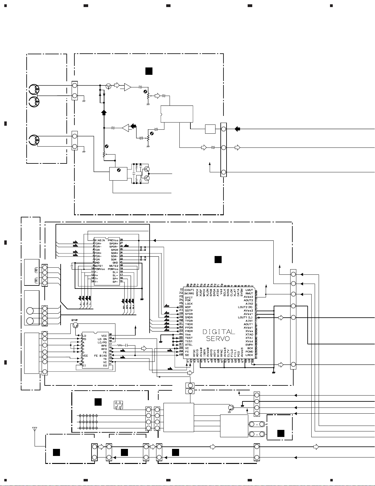
3. BLOCK DIAGRAM AND SCHEMATIC DIAGRAM
3.1 BLOCK DIAGRAM
A
MECHA ASSY
REC/PB
HEAD
ERASE
HEAD
CN2301
PB L
3
GND
2
CN2302
ERASE
1
GND
2
Q2301
(2SK373)
DS
G
(REC)
6
(NJM4558M)
PB
(BA4558MD)
+
VR2801
(BIAS)
5
L2801
BIAS OSC
B
(TS)
TFDR
(TS)
TRDR
(FS)
FFDR
(FS)
CN1101
T +
1
F -
2
F +
3
T -
4
CN1301
SL +
1
SL -
2
SP +
5
SP -
6
CN1101
LD ON
12
LD PD
9
PDIC PD1
7
PDIC PD2
6
F
15
E
8
VC
14
FRDR
(TS)
(TS)
IC1101
CXA1821M
IC1301
BA5970FP
(FS)
(FS)
FRONT PANEL
ASSY
K
KEY
(FS)
(TS)
JOG
CD MECHA ASSY
(2/2)
PICKUP ASSY
SL/SP
C
MOTOR
+
SL
-
+
SP
-
(1/2)
PICKUP ASSY
D
(TX)
TX CONNECT
7
2
TUNER MODULE
A
CN6201 CN161 J60
TX LcH
7
TX+5V
2
IC2301
3
+
2
-
IC2401
1
(SM)
(SM)
ASSY
B
DECK ASSY
+
1
VR2301
(PB LEVEL)
(REC)
3
2
+
1
3
(SM)
(CS)
(CS)
GNDCDM
V+5CD
CN150 CN50
JOG
KEY 1
KEY 2
KEY 3
TX LcH
TX+5V
J
(PB)
VR2401
(REC LEVEL)
Q2801
(2SC1815)
Q2802
(2SC1815)
TFDR
TRDR
FFDR
FRDR
10
10
17
17
13
13
15
15
J60
7
(TX)
2
+
3
IC2201
(HA1236AF)
DOLBY NR
8
REC OUT
+
(SM)
(CM)
(CM)
(TS)
(TS)
(FS)
(FS)
GND
(FS)
(TS)
44
38
PDG242A
SYSTEM U-COM
39
40
U-COM
ASSY
7
2
PB IN L
BIAS
Cro2
CD LD ON
CN10
CN10
IC5501
C
L2201
16
REC IN L
MPX
LINE OUT L
(PB)
V+12M
CD ASSY
15
15
13
AC_PLUS
60
49
LCD_CE
LCD_CLK
48 8
LCD_DATA
50 9
LCD_POW
414
(TX) (TX)
J2201
+
F
IC1201
CXD2587Q
7
REC L
5
PB L
4
V+12M
7
V+12TX
Q5501
GND
IC5503
PDG243
LCD U-COM
(PB)
(REC)
V+5.6U
GNDU
TX LcH
TX+5V
CN105
6
16
8
15
CN90
1 15
CN80
1 29
CN105
1
7
V+5CDM
V+5CD
V+5CD
D. OUT
V+12TX
GNDU
AC
V+5.6U
V+5UN
V+5CDM
GNDCDM
(CD)
(D.O)
GND
LCD
ASSY
D
V+5UN
V+5CD
CD L
D. OUT
J101
3
4
8
5
10
7
16
1234
Page 3
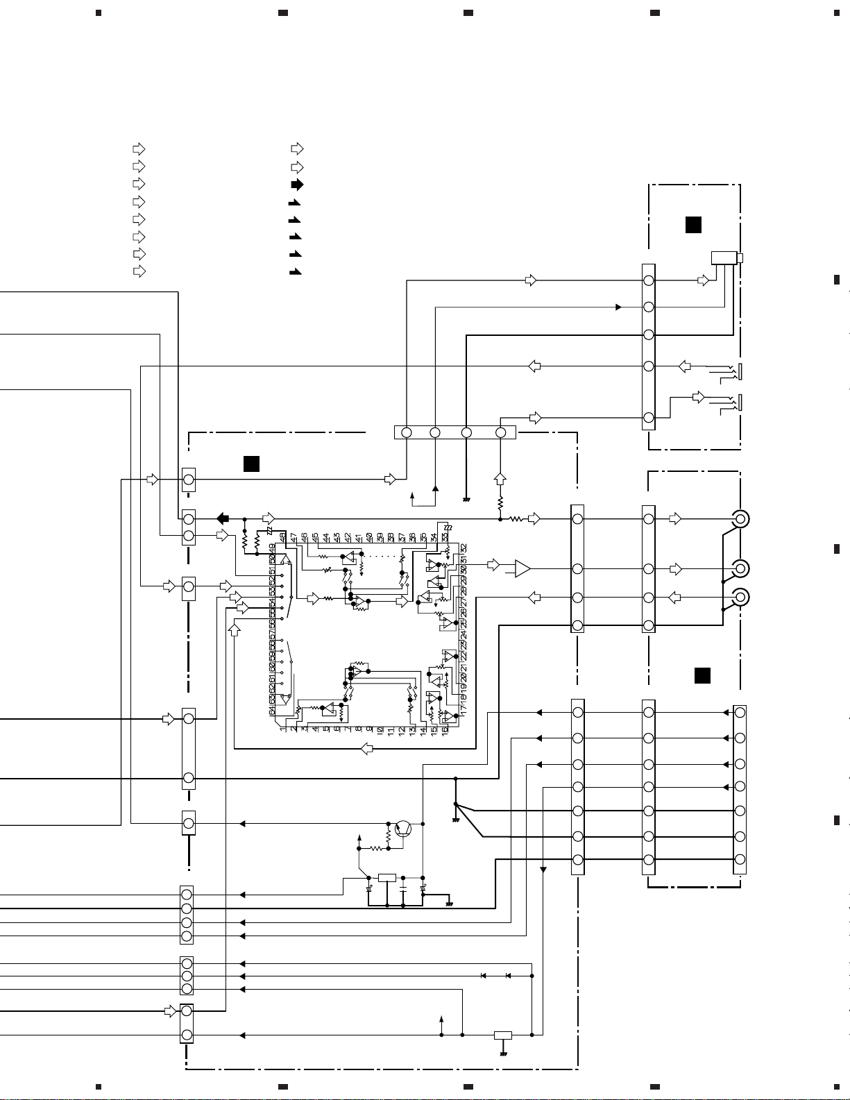
5
SIGNAL ROUTE
(CD)
: CD AUDIO SIGNAL
(L1)
: LINE 1 SIGNAL
(PB)
: DECK PB SIGNAL
(L2)
: LINE 2 SIGNAL
(MO)
: MAIN OUT SIGNAL
(D.O)
: OPTICAL OUT SIGNAL
(TX)
: TUNER AUDIO SIGNAL
(LO1)
: LINE OUT 1 SIGNAL
67
(LO2)
: LINE OUT 2 SIGNAL
(LO)
: LINE OUT SIGNAL
(REC)
: RECORDING SIGNAL
(FS)
: FOCUS SERVO LOOP LINE
(TS)
: TRACKING SERVO LOOP LINE
(SM)
: SPINDLE MOTOR ROUTE
(CM)
: CARRIAGE MOTOR ROUTE
(LM)
: LOADING MOTOR ROUTE
F- TERMINAL
ASSY
J103
(D.O) (D.O)
(L2)
V IN
VCC
GND OPT
LIN2
8
9
7
2
XC-IS21T
I
123
(L2)
8
A
OPT OUT
LINE IN2
(D.O)
(L2)
(CD)
(TX)
CN1
CN2
CN3
CN1
10
CN2
CN5
18
8
16
9
CN1
3
4
8
CN5
23
17
7
5
4
2
5
7
D. OUT
REC L
PB L
(PB)
LIN2
(L2)
CD L
GNDCDM
V+12M
V+12TX
GNDU
AC
V+5.6U
V+5UN
V+5CDM
V+5CD
TX LcH
TX+5V
(CD)
(REC)
(TX)
E
(L1)
(LO)
PB L
LIN 2
CD L
TX L
LIN1
AF ASSY
+
(MO)
CN3
(D.O)
IC3001
(LC75398NE)
(L1)
(2SD2395)
VDD
(NJM7812FA)
89 1
OPT IN/OUT
V+5
(MO)
Q2001
IC131
V+5 OPT
V+5
7
GND OPT
+
LOUT2
IC3002
(NJM4558MD)
(MO)
D3009D3008
IC141
(NJM7805FA)
(LO2)
(LO2)
3
2
(LO1)
+
-
CN32
LOUT1
AOUT L
1
12
LIN1
(L1) (L1)
GNDS
LOUT2
9
LOUT1
AOUT L
6
7
CN31
V+12UNV+12UN
9
AC
8
V+5.6V V+5.6V
7
V+5UN
10
B2GND
B1GND
GNDU
3
2
6
B2GND
B1GND
LIN1
GNDS
V+5UN
GNDU
CN132
12
CN131
AC
10
1
9
6
7
9
8
7
3
2
6
(LO2)
(LO1)
(MO)
R- TERMINAL
ASSY
H
CN7101
1
3
4
5
6
9
10
LINE OUT2
LINE OUT1
AUDIO OUT
LINE IN1
V+12UN
AC
V+5.6V
V+5UN
(M-IS21)
B2GND
TO. STEREO PWER AMPLIFIER
B1GND
GNDU
B
C
D
17
5
6
7
8
Page 4
1
234
XC-IS21T
3.2 OVERALL CONNECTION DIAGRAM
A
CN1
B
J101
F
(AWU7305)
F-TERMINAL ASSY
I
E
CD ASSY
(AWU7311)
AF ASSY
(AWU7298)
CN1301
J111
J103
CN3
J107
CN7
CN11
G
CD MOTOR
ASSY
(AWU7318)
CN1101
CN6201
C
CN161
J60
J60
A
B
CN110
(AXQ7065)
(AWU7323)
FM/AM TUNER MODULE
D
CN190 CN180
TX CONNECT ASSY
D
CN10
LCD ASSY
(AWU7354)
U- COM ASSY
CN80CN90
C
(AWU7327)
18
1234
Page 5
5
67
8
XC-IS21T
Note : When ordering service parts, be sure to refer to "EXPLODED VIEWS and P AR TS LIST" or "PCB PARTS LIST".
To. OPTION DECK
CN132
CN32
CN5
CN105
C
CN7102 CN7101
R-TERMINAL ASSY
U- COM ASSY
(AWU7327)
H
(AWU7315)
To. STEREO POWER AMP (M-IS21)
CN131
CN2
CN31
CN20
J2201
CN2603
CN2701
J2202
J
(AWU7334)
DECK ASSY
A
B
FRONT PANEL ASSY
K
CN51
J51
L
LIGHT-L ASSY
(AWU7321)
(AWU7308)
CN50
CN150
J155
N
CD CLOSE SW ASSY
J55
(AWU7320)
M
CD OPEN SW ASSY
J54J154
(AWU7319)
CN2301
CN2302
C
D
19
5
6
7
8
Page 6
1
234
XC-IS21T
3.3 FM/AM TUNER MODULE and TX CONNECT ASSYS
A
RF AMP
(FM) (FM)
B
(FM) (FM)
(FM)
(FM)
1T378A
OSC
1T378A
(FM)
MIX AMP
(FM) (FM) (FM)
BUFFER
(FM)
IF AMP
FM +B SW
(FM)
(AM) (AM) (AM)
(FM)
(AM)
C
(AM)
MW RF TUNING BLOCK
AKX7041
(AM)
FM/AM TUNER MODULE
(AXQ7065)
D
: AM SIGNAL ROUTE
(FM)
: FM SIGNAL ROUTE
(TX)
: TUNER AUDIO SIGNAL
20
A
1234
Page 7
5
67
8
XC-IS21T
A
(AM)
(FM)
(AM)
(FM)
(FM)
AF AMP
(TX) (TX)
AF AMP
REGULATOR
(TX)
CN161 J60
CN6201
D20PYY1315
B
(AWU7323)
B
C
J60
C
PLL
TX CONNECT ASSY
D
21
5
6
7
A
B
8
Page 8
1
XC-IS21T
3.4 U-COM and LCD ASSYS
A
CN190 CN180
234
D
LCD ASSY
(AWU7354)
CN90
B
L5509 L5510
C
CN80
C
U-COM ASSY
(AWU7327)
D
CN20
J2202
J
22
C
D
1234
Page 9

5
67
8
XC-IS21T
K
CN150
IC5501
PDG242
CN50
B
J60
A
J60
5.6
SIGNAL ROUTE
(TX)
: TUNER AUDIO SIGNAL
(TX)
L5508
L5544
L5507
CN105
B
E
CN5
L5506
L5505
L5504
L5504 -L5506
LINE 2 MUTE
LINE CONT
LINE 1 MUTE
(TX)
C
CN10
F
CN110
D
23
5
6
7
C
8
Page 10

XC-IS21T
3.5 AF ASSY
A
1
234
CN7J107
B
J101
J2201
C
F
J
CN1
CN2
E
(PB)
(REC)
AF ASSY
(AWU7298)
(CD)
(TX)(TX)
(CD)
(L1)
(TX)
(REC)
(PB)
(L2)
(CD)
(TX)
(L1)
(PB)
(L2)
(LO)
(L2)
(LO)
(MO)
(L1)
(PB)
(REC)
(L1)(L1)
SIGNAL ROUTE
(CD)
: CD AUDIO SIGNAL
(L1)
: LINE 1 SIGNAL
(PB)
: DECK PB SIGNAL
(L2)
: LINE 2 SIGNAL
(MO)
: MAIN OUT SIGNAL
(TX)
: TUNER AUDIO SIGNAL
(LO1)
D
: LINE OUT 1 SIGNAL
(LO2)
: LINE OUT 2 SIGNAL
(LO)
: LINE OUT SIGNAL
(REC)
: RECORDING SIGNAL
24
E
(TX)
C
CN5
CN105
1234
Page 11

CN3
5
67
8
XC-IS21T
I
J103
(LO1)
(MO))
(LO)
(L2)
VTL1105
0
VTL1105
(L2)
(LO2)
0
(LO1)
A
CN31
H
CN131
100
(LO1)
(MO)(MO)(MO))
(LO1)
B
100
(L1)
S5688G
S5688G
(L1)(L1)
H
CN132
CN32
C
D
5
6
7
8
E
25
Page 12

1
234
XC-IS21T
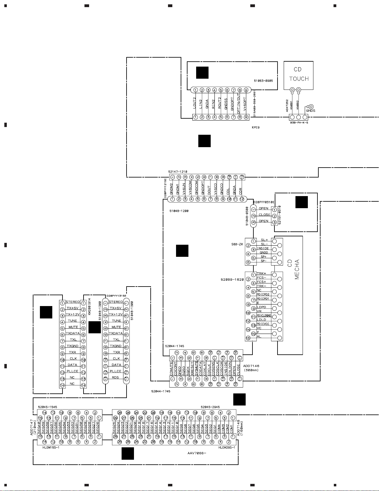
3.6 CD and CD MOTOR ASSYS
A
(SM)
B
(FS)
(FS)
(TS)
(TS)
(SM)
(SM)
(CS)
(CS)
F
CD ASSY
(AWU7305)
(FS)
(SM)
(CM)
(CM)
(TS)
(TS)
(FS)
(FS)
C
To. P.U Assy
D
CN1301
To. CD MECHA
CN1101
(LM)
(LM)
(SM)
(SM)
(TS)
(FS)
(FS)
(TS)
Note: The encircled numbers denote measuring point in the schematic diagram.
IC1101- Pin 16:
1
PLAY MODE (RF)
H : 500nsec/div
1.0Vp-p
VC
IC1101- Pin 13 :
2
TEST MODE,
Tracking Open (TRER)
H : 5msec/div
VC : IC1101- Pin12
1.0Vp-p
VC
1
(FS)
2
(TS)
VC
(TS)
26
SIGNAL ROUTE
: CD AUDIO SIGNAL ROUTE
(FS)
: FOCUS SERVO LOOP LINE
(TS)
: TRACKING SERVO LOOP LINE
(SM)
: SPINDLE MOTOR ROUTE
(CM)
: CARRIAGE MOTOR ROUTE
(LM)
: LOADING MOTOR ROUTE
F
1234
Page 13

(SM)
(CM)
(CM)
(TS)
(TS)
(FS)
(FS)
5
67
8
XC-IS21T
A
J101
E
CN1
B
(FS)
(TS)
C
CN10
CN110
C
CD MOTOR ASSY
G
CN11J111
(AWU7318)
D
5
6
7
8
GF
27
Page 14

1
234
XC-IS21T
3.7 R-TERMINAL and F-TERMINAL ASSYS
A
H
CN7101
(AWU7315)
CN131
E
CN31
(M-IS21)
B
TO. STEREO POWER AMPLIFIER
R- TERMINAL ASSY
(L1)
VTL1096
VTL1096
(L1)
VTL1096
VTL1096
(MO)
(LO1)
(L1)
E
CN32
(LO1)
C
(MO) (MO)
D
VTL1096
CN7102
VTL1096
VTL1096
CN132
SIGNAL ROUTE
(MO)
: MAIN OUT SIGNAL
(L1)
: LINE 1 SIGNAL
(LO1)
: LINE OUT1 SIGNAL
To. OPTION DECK
28
H
1234
Page 15

1
F- TERMINAL ASSY
I
(AWU7311)
23
XC-IS21T
SIGNAL ROUTE
(L2)
: LINE2 SIGNAL
(LO2)
: LINE OUT2 SIGNA
4
A
B
(L2)
(L2)
(L2)(L2)
(LO2)
C
(LO2)
(LO2)
J103
D
E
CN3
29
1
2
3
I
4
Page 16

1
XC-IS21T
3.8 DECK ASSY
234
A
CN2301
CN2302
B
J
(PB)
(REC) (REC)
DECK ASSY
(AWU7334)
(PB)
(PB)
(PB)
(PB)
(REC)
(REC)
SIGNAL ROUTE
(PB)
: PB SIGNAL
(REC)
: RECORDING SIGNAL
C
D
30
J
1234
Page 17

5
67
8
XC-IS21T
A
X
J2201
(PB)
(REC)
(PB)
(REC)
(PB)
(PB)
(REC)
(PB)
E
CN2
(REC)
J2202
B
C
CN20
CN2603
5
C
CN2701
D
6
7
8
J
31
Page 18

1
234
XC-IS21T
3.9 FRONT PANEL, LIGHT-L, CD OPEN SW and CD CLOSE SW ASSYS
A
CN150
B
J51
CN51
C
CN50
L
LIGHT-L ASSY
(AWU7321)
DTA143EK-TLB
C
DTC124EK-TLB
SLR-343VC(NPQ)-TS
DTC124EK-TLB
K
FRONT PANEL ASSY
(AWU7308)
D
32
K
L
1234
Page 19

5
FRONT PANEL ASSY (SW name)
S5901: POWER (STANDBY/ON)
S5902: DISPLAY/RDS
S5903: TIMER REC/WAKE UP
S5904: TAPE/OPEN/CLOSE
S5905: TAPE
S5906: LINE1, 2
S5907: /TUNING+
S5908: REC/STOP
67
S5909: TREBLE
S5910: PLAY/PAUSE
S5911: ST.WIDE
S5912: BASS
S5913: STOP
S5914: BALANCE
S5915: TUNER
S5916: VOLUME/JOG
S5917: /TUNINGS5918: BALANCE
S5919: CD
S5920: STATION MEMORY
S5921: FREQ/STATION
S5922: REVERSE
S5923: DOLBY NR ON/OFF
8
XC-IS21T
A
B
C
J154
J54
M
CD OPEN SW ASSY
(AWU7319)
5
6
N
CD CLOSE SW ASSY
(AWU7320)
J155
J55
D
NM
7
8
33
Page 20

XC-IS21T
4. PCB CONNECTION DIAGRAM
NOTE FOR PCB DIAGRAMS :
1. Part numbers in PCB diagrams match those in the schematic
diagrams.
2. A comparison between the main parts of PCB and schematic
diagrams is shown below.
Symbol In PCB
Diagrams
BCE
BCE
D
Symbol In Schematic
Diagrams
BCEBCE
BCE
DGGSS
BCE
DGS
Part Name
Transistor
Transistor
with resistor
Field effect
transistor
Resistor array
3. The parts mounted on this PCB include all necessary parts for
several destinations.
For further information for respective destinations, be sure to
check with the schematic diagram.
4. View point of PCB diagrams.
Connector
Capacitor
SIDE A
P.C.Board
Chip Part
SIDE B
3-terminal
regulator
34
Page 21

6. ADJUSTMENT
For adjustment, use the stereo power amplifier (M-IS21).
6.1 DECK SECTION
6.1.1 Adjustment Condition
(1) The ground at the time of adjustment shall be W166.
(Refer to Fig. 6–3).
(2) Clean the heads and demagnetize them using a head eraser.
(3) Set the measurement level to 0 dBV = 1 Vrms.
(4) Use the specified tape for adjustment. Use the labeled (A) side
of the test tape.
NCT–111 : For Tape Speed adjustment
STD-331E : For Playback adjustment
STD–632 : Normal blank tape
* As the reference recording level is 250 nwb/m for STD–
331E, the recording level will be higher by 4 dB for STD–
331B (160nwb/m). When adjusting, pay carefull attention
to the type of tape used.
(5) Provide yourself with the following measuring devides:
÷ AC millivoltmeter
÷ Low-frequency oscillator
÷ Attenuator
÷ Oscilloscope
(6) Adjust both right and left channels unless otherwise specified.
(7) Turn the DOLBY NR switch off unless otherwize specified.
(8) Warm up the unit for several minutes before adjustment. In
particular, be sure to warm up the unit in the REC/PLAY mode
for 3 to 5 minutes before starting recording/playback frequency
characteristics adjustment.
(9) Always follow the indicated adjustment order.
Otherwise, a complete adjustment may not be achieved.
7 List of Adjustments
¶ Playback Section
(1) Tape Speed Confirmation
(2) Head Azimuth Adjustment
(3) Playback Level Adjustment
¶ Recording Section
(1) Recording Bias Adjustment
(2) Recording Level Adjustment
PLAY BACK
250
3dB
RECORDING
250
3dB
10k
3dB 4dB
10k
3dB
XC-IS21T
12.5k
12.5k
5dB
0 dB
30s
315 Hz
Fig. 6-1 Frequency Characteristics
Dolby noise reduction manufactured under license from Dolby
Laboratories Licensing Corporation.
“DOLBY” and the double-D symbol are trademarks of Dolby
Laboratories Licensing Corporation.
0 dB: 315 Hz, 250 nwb/m
30 s 30 s 30 s 10s 10s .......................................................................................................... 10s
6.3 kHz 10 kHz 315 Hz 14 kHz
12.5
kHz
10 kHz
6.3
8 kHz 4 kHz 2 kHz
kHz
1 kHz
500Hz250Hz125
Hz
63 Hz 40 Hz
Fig. 6-2 Test Tape STD– 331E
–20 dB
51
Page 22

XC-IS21T
6.1.2 Playback Section
(1) Tape Speed Confirmation
No. Mode Input Signal/Test Tape Adjustment Points Measurement Points Adjustment Value Remarks
PLAY1
NCT-111 (3 kHz)
VR2701 (DECK ASSY)
(Refer to Fig. 6-3)
TP R (C2204)
(DECK ASSY)
(2) Head Azimuth Adjustment
¶ This unit is equipped with auto tape selector.
¶ Do not switch between forward and reverse operation with the screwdriver inserted.
No. Mode Input Signal/Test Tape Adjustment Points
Measurement
Points
3000 Hz Hz
Adjustment
Value
+10
–10
FWD adjustment
REV Confirmation
( 3000 Hz Hz )
Remarks
+60
–60
PLAY1
STD-331E test tape
(Playback: 10 kHz, –20 dB)
Head azimuth
adjustment Screw
(Refer to Fig. 6-3)
TP L (C2203)
TP R (C2204)
(DECK ASSY)
Max. Playback
signal level
(3) Playback Level Adjustment
¶ Since this adjustment determines playback DolbyNR level, Perform it carefully.
Measurement
Points
1
PLAY
STD-331E test tape
(Playback: 315 Hz, 0 dB)
L ch
R ch VR2302
VR2301
TP L (C2203)
TP R (C2204)
(DECK ASSY)
Adjustment
Value
–3.7 dBV
6.1.3 Recording Section
(1) Recording Bias Adjustment
¶ After the adjustment, caution should be exercised so as not to become under bias by checking the distortion rate.
No. Mode Input Signal/Test Tape Adjustment Points
REC/
1
PAUSE
REC =
2
PLAY
Input a 315Hz signal to the LINE -
IN terminal. ∗
Load the STD–632 test tape and
record/playback the 315Hz and
10kHz signals. (see the Note below)
Input signal level –23.7 dBV
L ch
R ch VR2802
VR2801
Measurement
Points
TP L (C2203)
TP R (C2204)
(DECK ASSY)
Adjustment
Value
Repeat adjustment until playback level of
the 10kHz signal is within 0.5dBV ±0.5dB
from that of the 315Hz signal.
After adjustment, apply silicon
bond to the head azimuth
adjustment screw.
RemarksNo. Mode Input Signal/Test Tape Adjustment Points
Remarks
Note: Set the 10kHz input signal level to the same value as the 315Hz input signal level of step 1.
(2) Recording Level Adjustment
No. Mode Input Signal/Test Tape Adjustment Points
REC/
1
PAUSE
REC =
2
PLAY
Input a 315Hz signal to the LINE-
IN terminal.∗
STD–632 test tape and record/
playback the 315Hz signal.
Input signal level –7.7 dBV
L ch
R ch VR2402
VR2401
52
Measurement
Points
TP L (C2203)
TP R (C2204)
(DECK ASSY)
Adjustment
Value
Repeat recording, playback and
adjustment until playback level of the
315Hz signal becomes –
Remarks
7.7dBV±0.5dB
.
Page 23

7. GENERAL INFORMATION
7.1 DIAGNOSIS
7.1.1 SEQUNCE AFTER THE POWER ON
XC-IS21T
Note 1 : IC No. or P∗∗ without name indicate the pin No.
of microcomputer.
Standby states
POWER ON
Power is ON.
Transmit the bus data.
Initialize the LCD microcomputer.
DECK control IC starts
the data transfer.
Does CD door open ?
Is P9 and P10 at "H" level ?
Close the CD door.
Initialize the DECK.
Yes
P35 SYSPOWER : "H"
System bus communication (∗1)
Transfer the system POWER ON.
P4 LCD POWER ON : "H"
P53 LCDRST : "L" RESET
Starts the LCD communication (∗2)
Microcomputer
No
P11 : "H"
P28 VOLDATA
P34 VOLCLK
P75 EXPCE
DECK Initialize Sequence
Note ;
∗1 : System bus communication
∗2 : Starts the LCD communication
∗3 : Transfer the Function, Volume, BASS
and TREBLE data to the volume IC.
∗4 : Initial setting of CD decoder IC
∗5 : Initialize the TUNER PLL IC
Transfer
MOTOR ON
Does the DECK Head down ?
(Is the MODE SW OFF ?)
P29 SYSCLK
P46 SYSDATA
P47 SYSREQ
P48 LCDCLK
P49 LCDCE
P50 LCDDATA
P27 VOLCE
P28 VOLDATA
P34 VOLCLK
P17 CDCLK
P18 CDLAT
P19 CDDATA
P65 TXCE
P66 TXODAT
P67 TXCLK
P68 TXIDAT
Check P79 MODE SW
input is "L".
Yes
Perform the following process after
one second after the POWER ON.
Transfer the Function, Volume, BASS
and TREBLE data to the volume IC. (∗3)
Function : CD (∗4)
Initial setting of CD decoder IC.
P22 CDCONT : "L"
Perform the following process after
3.9 seconds after the POWER ON.
Release the system MUTE.
P71 SYSMUTE : "H"
Perform the following process after
4.0 seconds after the POWER ON.
Release the speaker relay.
P70 SPCONT : "H"
Function : TUNER (∗5)
Initialize the TUNER PLL IC.
P64 TXPOW : "H"
The condition that MUTE
is not released.
• VOLUME : 0
• DECK Function : excepting PLAY
No
Is three times ?
No
500 msec.
solenoid is ON ?
MOTOR OFF
Yes
IC2601(BU4094) P12 is "H"
IC2601(BU4094) P11 is "L"
Retry it to two times.
57
Page 24

XC-IS21T
7.1.2 SINGLE OPERATION METHOD
Jigs and Measuring instruments
A
V
Low-frequency
oscillator
DC power-
supplay
Single operation method and frequnency oscilator inputlevel.
1. Connect part A of the AF ASSY [W420(+8V),W421 (+15V), W422 (+5.6V), W423(GND) and DC power-supplay.
(Refer to Fig. 7-1.)
DC power-supplay
Connect point A Voltage (V) Remarks
AF ASSY, W420 (+8v) +8V
AF ASSY, W421 (+15v) +15V
AF ASSY, W422 (+5.6v) +5.6V
AF ASSY, W423 (GND) GND
2. Connect part B of the U-COM ASSY [ CN105 pin8 (AC), AF ASSY[W423 (GND)] and frequency oscillator.
(Refer to Fig. 7-1 and 7-2.)
Low-frequency oscillator
Connect point B frequency level Gnd Remarks
U-COM ASSY, CN105 pin8 (AC) 50 or 60 Hz Approx.2.0 Vrms Note.
AF ASSY, W423 (GND) osc GND
Note: Set up the low-frequncy oscillator level with in the limits of product moves.
58
 Loading...