

Page 1
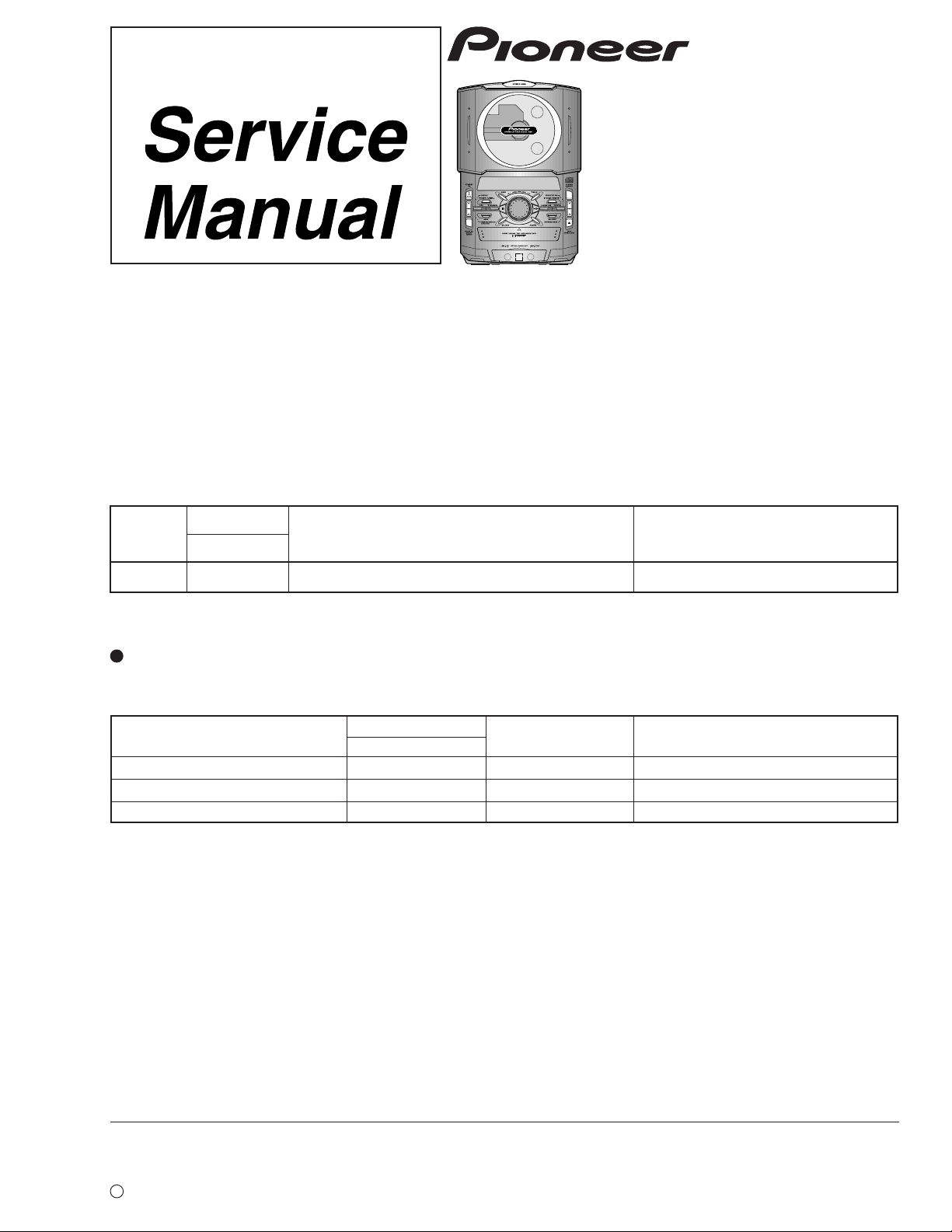
CD TUNER DECK
XC-IS21T
THIS MANUAL IS APPLICABLE TO THE FOLLOWING MODEL(S) AND TYPE(S).
ORDER NO.
RRV2148
Type
ZUCXJ O DC power supply from other system
Model
XC-IS21T
Power Requirement
Remarks
This product is a system(s) component.
This product does not function properly when independent; to avoid malfunctions, be sure
to connect it to the prescribed system component(s), otherwise damage may result.
Component
CD TUNER DECK XC-IS21T RRV2148 This service manual
STEREO POWER AMPLIFIER M-IS21 RRV2143
SPEAKER SYSTEM S-IS21 RRV2141
System
IS-21T
Service Manual Remarks
CONTENTS
1. SAFETY INFORMATION
2. EXPLODED VIEWS AND PARTS LIST
3. BLOCK DIAGRAM AND SCHEMATIC DIAGRAM 16
4. PCB CONNECTION DIAGRAM
5. PCB PARTS LIST
6. ADJUSTMENT
7. GENERAL INFORMATION
................................................
.....................................................
.......................................
.................
...........................
..................................
34
46
51
57
2
3
7.1 DIAGNOSIS
7.1.1 SEQUNCE AFTER THE POWER ON
7.1.2 SINGLE OPERATION METHOD
7.1.3 DISASSEMBLY
7.1.4 PCB LOCATION
7.2 PARTS
7.2.1 IC
8. PANEL FACILITIES AND SPECIFICATIONS
...................................................
..........
....................................
...................................
...........................................................
..........................................................
.......
...
57
57
58
60
64
65
65
70
PIONEER ELECTRONIC CORPORATION 4-1, Meguro 1-Chome, Meguro-ku, Tokyo 153-8654, Japan
PIONEER ELECTRONICS SERVICE, INC. P.O. Box 1760, Long Beach, CA 90801-1760, U.S.A.
PIONEER ELECTRONIC (EUROPE) N.V. Haven 1087, Keetberglaan 1, 9120 Melsele, Belgium
PIONEER ELECTRONICS ASIACENTRE PTE. LTD. 253 Allexandra Road, #04-01, Singapore 159936
c
PIONEER ELECTRONIC CORPORATION 1999
T – ZZY MAY 1999 Printed in Japan
Page 2

XC-IS21T
1. SAFETY INFORMATION
This service manual is intended for qualified service technicians; it is not meant for the casual
do-it-yourselfer. Qualified technicians have the necessary test equipment and tools, and have been
trained to properly and safely repair complex products such as those covered by this manual.
Improperly performed repairs can adversely affect the safety and reliability of the product and may
void the warranty. If you are not qualified to perform the repair of this product properly and safely, you
should not risk trying to do so and refer the repair to a qualified service technician.
WARNING
This product contains lead in solder and certain electrical parts contain chemicals which are known to the state of California to cause
cancer, birth defects or other reproductive harm.
IMPORTANT
THIS PIONEER APPARATUS CONTAINS
LASER OF CLASS 1.
SERVICING OPERATION OF THE APPARATUS
SHOULD BE DONE BY A SPECIALLY
INSTRUTED PERSON.
Health & Safety Code Section 25249.6 – Proposition 65
LASER DIODE CHARACTERISTICS
MAXIMUM OUTPUT POWER: 5 mw
WAVELENGTH: 780-785 nm
2
Page 3
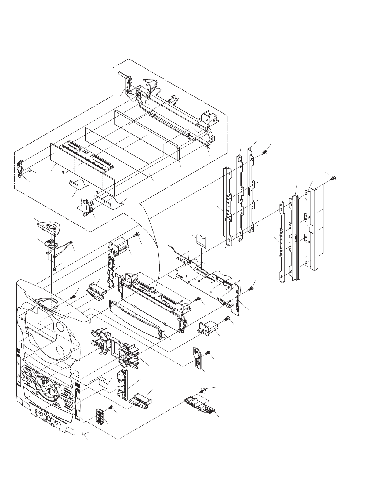
2. EXPLODED VIEWS AND PARTS LIST
NOTES:• Parts marked by "NSP" are generally unavailable because they are not in our Master Spare Parts List.
The mark found on some component parts indicates the importance of the safety factor of the part.
•
Therefore, when replacing, be sure to use parts of identical designation.
Screws adjacent to mark on the product are used for disassembly.
•
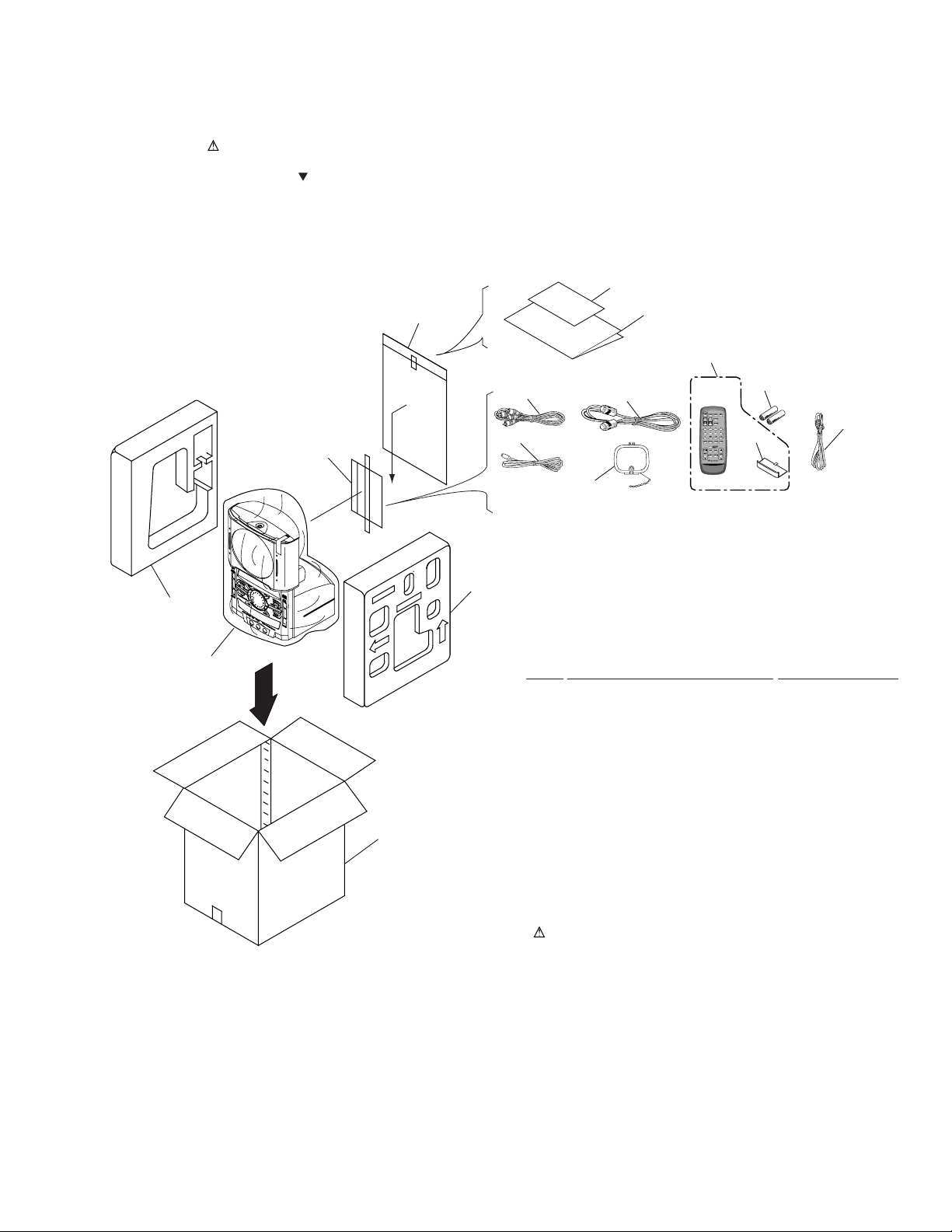
2.1 PACKING
7
XC-IS21T
15
17
13
13
16
3
9
11
19
2
10
1
8
(1) PACKING PARTS LIST
Mark No. Description Part No.
1 System Cable ADE7039
2 FM Antenna ADH7004
3 Operating Instructions ARE7224
(English/ French)
4 • • • • •
5 • • • • •
12
18
NSP 7 Warranty Card ARY7033
6 • • • • •
8 AM Loop Antenna ATB7007
9 Remote Control Unit AXD7224
(CU-XR056)
10 RCA Pin- plug Stereo Cable VDE1052
(L= 1.5m)
NSP 11 Dry Cell Batteries(AA/R6) VEM-013
12 Power Cord XDG3007
13 Polyethylene Bag Z21-038
(0.03 x 230 x 340)
14 • • • • •
15 Side Pad ML AHA7240
16 Side Pad MR AHA7241
17 Packing Sheet AHG7053
18 Packing Case AHD7751
19 Battery Cover AZA7331
3
Page 4
XC-IS21T
2.2 EXTERIOR (1/2)
Refer to "2.4 FRONT PANAEL ASSY (1/2)
and 2.5 FRONT PANEL ASSY (2/2)"
13
1
10
10
11
12
10
9
9
2
9
8
4
5
3
8
7
6
2
4
Page 5

(1) EXTERIOR (1/2) PARTS LIST
Mark No. Description Parts No.
1 Rear Cover AMC7029
2 Cussion Rubber AEB7154
3 Jack Door AAN7188
4 Jog Lens AAK7651
5 Jog Knob AAA7005
XC-IS21T
NSP 7 Tray Seal RRW1162
NSP 12 Name Label AAL7231
6 Tray Cap AAK7622
8 Jog Escutcheon AAK7620
9 Screw BBZ30P080FMC
10 Screw VPZ30P100FMC
11 Screw BMZ30P060FZK
13 Label M ARW7065
5
Page 6
XC-IS21T
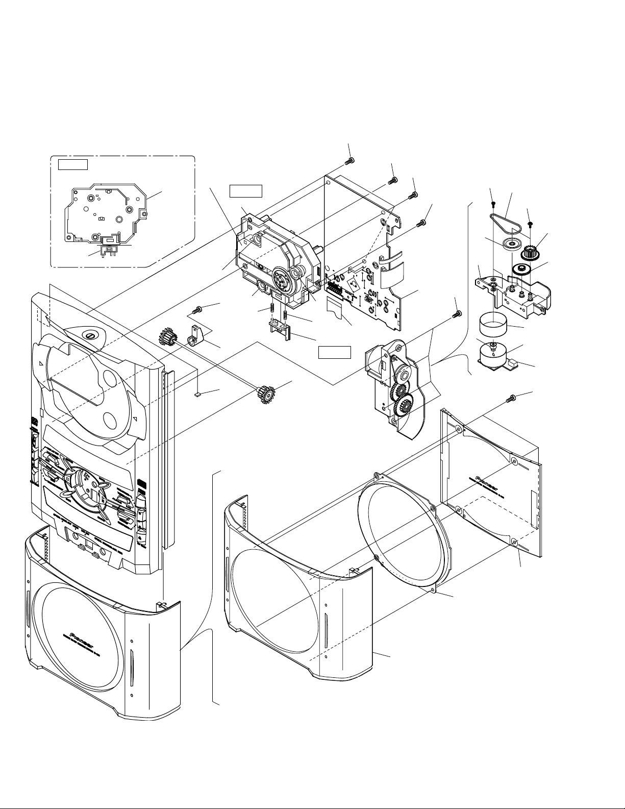
2.3 EXTERIOR (2/2)
21
21
Refer to
" 2.7 DECK MECHANISM
UNIT "
2
7
21
1
6
22
22
23
24
19
4
A
21
17
16
21
18
9
21
20
15
3
10
A
8
12
25
5
11
22
6
Page 7

÷ EXTERIOR (2/2) PARTS LIST
Mark No. Description Parts No.
1 U- COM ASSY AWU7327
2 DECK ASSY AWU7334
3 AF ASSY AWU7298
4 R- TERMINAL ASSY AWU7315
5 FM/AM TUNER MODULE AXQ7065
6 Deck Shield AEC7209
7 DECK MECHANISM UNIT AXA7075
NSP 8 Chassis M ANA7087
9 Rear Panel ANC7735
NSP 10 Shield Plate ANK7059
11 Shield Case T ANK7050
12 Shield Case B ANK7051
13 • • • • •
14 • • • • •
15 PC Support DEC1932
NSP 16 Spacer AEB7092
17 Rubber Sheet AEB1111
18 Leg Assy IS AEC7202
19 Locking Card Spacer VEC1596
NSP 20 PCB Spacer (3 x 6) AEC7156
XC-IS21T
21 Screw BBZ30P080FMC
22 Screw VPZ30P080FZK
23 Connector Assy 3p ADX7252
24 23P F.F.C /30V ADD7150
NSP 25 TX CONNECT ASSY AWU7323
7
Page 8
XC-IS21T
2.4 FRONT PANEL ASSY (1/2)
6
33
5
10
33
33
13
14
7
8
9
27
14
27
13
24
25
29
11
26
29
33
10
19
32
18
12
16
22
29
21
23
20
30
29
15
15
34
1
29
17
29
2
28
29
3
31
8
4
Page 9

÷ FRONT PANEL ASSY (1/2) PARTS LIST
Mark No. Description Parts No.
1 FRONT PANEL ASSY AWU7308
NSP 2 CD CLOSE SW ASSY AWU7320
NSP 3 CD OPEN SW ASSY AWU7319
4 F- TERMINAL ASSY AWU7311
NSP 5 LCD ASSY (TC) AWU7354
XC-IS21T
NSP 6 LIGHT- L ASSY AWU7321
7 Lens Holder M AMR7247
8 Lens M AAK7615
9 Diffusion Sheet AAK7666
10 Reflector AMR7248
11 15P F.F.C/ 30V ADD7147
12 29P F.F.C/ 30V ADD7148
13 Frame ANG7235
14 Rail AMR7239
15 Blind AMR7261
16 PCB Holder L AMR7262
17 PCB Holder R AMR7263
18 Plating Button Assy AXG7089
19 Fuction Button B AAD7511
20 Window AAK7621
21 Complex Button AAD7509
22 Plating Button A AAD7567
23 Function Button A AAD7510
24 O/C Button AAD7506
25 Key O/C AAD7526
26 Connector 3p ADX7252
27 Screw IPZ30P100FMC
28 Screw ABA1005
29 Screw VPZ30P080FZK
30 17P F.F.C/ 30V ADD7145
31 Front Panel M AMB7565
32 PU Caution Label ARW7059
33 Spacer AEC7216
34 Screw VPZ30P100FMC
9
Page 10
XC-IS21T
2.5 FRONT PANEL ASSY (2/2)
27
Note 1 Cutting Position
(No.13 (Mecha Holder)
No.13
(2/2)
Cutting
No.13
(1/2)
Refer to
"2.6 CD MECHANISM ASSY"
11
Note 1
13 (1/2)
25
25
21
12
18
17
19
25
12
13 (2/2)
Note 1
26
20
21
23
10
27
9
6
2
21
24
8
7
C
A
B
4
5
3
1
22
10
14
15
16
Page 11

÷ FRONT PANEL ASSY (2/2) PARTS LIST
Mark No. Description Parts No.
1 CD MOTOR ASSY AWU7318
2 CD ASSY AWU7305
3 Slider Motor VXM1033
NSP 4 Motor Shield ANK7067
5 Motor Pulley PNW1634
6 Gear Holder AMR7240
7 Gear A ANW7063
8 Gear B AMR7260
9 Gear Pulley A ANW7066
10 Belt AEB7171
11 CD MECHANISM ASSY KSM-620AAA
12 Float Spring ABH7170
13 Mechanism Holder AMR7242
14 CD Door Window AAK7618
15 CD Door Escutcheon AAK7619
16 CD Door AAN7189
17 Shaft Assy AXG7078
18 Shaft Holder AMR7237
19 Cussion Rubber AEB7154
20 Screw BBZ30P080FMC
XC-IS21T
21 Screw VPZ30P080FZK
22 Screw ABA7054
23 Screw PMZ26P040FMC
24 Screw IPZ20P080FMC
25 Float Rubber AEB7129
26 17P F.F.C/ 30V ADD7146
27 Screw VPZ30P100FMC
11
Page 12
XC-IS21T
2.6 CD MECHANISM ASSY
2
10
6
1
5
8
7
9
3
4
÷ CD MECHANISM ASSY PARTS LIST
Mark No. Description Parts No.
1 KSS-620A(RP) 8-820-063-(03)
2 Sled Screw Assy X-2646-389-(1)
3 Sled Motor Assy A-4912-199-(A)
4 MD Assy X-2646-482-(1)
5 Geer BN 2-627-751-(02)
6 Rack Spring 2-646-912-(01)
7 Holder 2-646-913-(01)
8 Tapping Screw 2-646-352-01
9 Precision Screw 2-627-668-01
10 Tapping Screw 2-646-358-11
12
Page 13
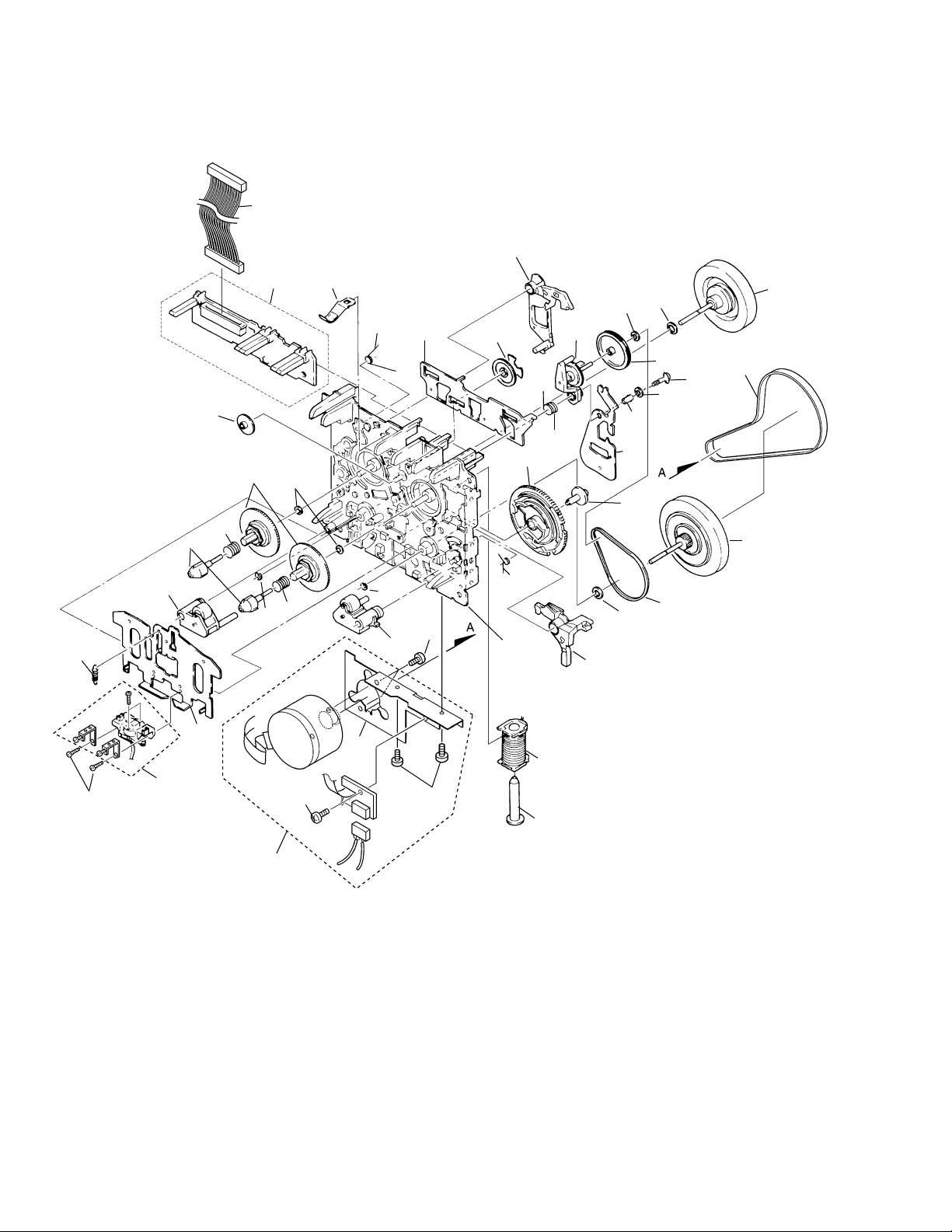
2.7 DECK MECHANISM UNIT (1/2)
17
XC-IS21T
6
5
16
16
14
13
12
4
3
16
18
16
8
1
11
9
4
16
10
2
Refer to "2.8 DECK MECHANISM UNIT (2/2)".
÷ DECK MECHANISM UNIT (1/2) PARTS LIST
Mark No. Description Parts No.
1 Screw FG114-14
2 Screw UG12H-15
3 Front BKT FC64K-11
4 Washer MJ112-22
5 SP Return FK34N-11
6 Plate Hold BLK F573-258
7 Holder CST BLK F527-078
8 LDG Base FD56R-12
9 Pulley FD56T-11
10 LDG Gear FD56U-11
2
7
Mark No. Description Parts No.
11 Slider FD57E-11
12 LDG Belt FF19L-12
13 Switch UE15S-14
14 MTR Reel BLK F564-313
15 • • • • •
16 Screw UG12H-28
17 SP Clamper FK34M-11
18 Switch UE18P-21
13
Page 14
XC-IS21T
2.8 DECK MECHANISM UNIT (2/2)
39
33
40
19
15
12
10
4
2
32
8
30
23
5
14
31
32
7
3
18
34
11
6
16
35
21
24
41
42
43
37
36
26
30
13
20
27
22
17
28
1
1
29
9
25
3
38
14
Page 15

÷ DECK MECHANISM UNIT (2/2) PARTS
LIST
Mark No. Description Parts No.
1 Screw KG194-36
2 Reel Feather FD57D-13
3 Screw UG11S-14
4 SP Reel(L) FK32U-12
5 SP Brake FK33B-13
6 SP Arm Play FK33P-11
7 SP Reel(R) FK32V-12
8 Spring Cassette FC65M-11
9 BKT MTR FC64M-12
10 Reel Base FD52W-12
11 Cam Gear FD52Y-23
12 Play Gear (A) FD53K-12
13 Arm Play FD53D-19
14 Plate Slide FC61L-19
15 PCB Control BLK F567-617
16 Chassis base BLK F612-231
17 Head Base FC61K-32
18 Roller Pinch BLK R F514-129
19 Roller Pinch BLK L F514-130
20 Assy F/W FR24S-21
XC-IS21T
21 Clutch Assy BLK F522-037
22 Clutch Assy BLK F522-048
23 Washer FJ111-13
24 F/R Pulley FD53F-15
25 Solenoid BLK F765-279
26 F/R Belt FF18W-12
27 Belt Main FF19H-11
28 Plate HD BLK F513-824
29 MTR MAIN BLK F525-321
30 Washer FJ111-30
31 Washer FJ111-35
32 Washer UJ16F-11
33 Lever Brake FD53P-17
34 FF Gear(A) FD53L-12
35 Cam SP FK32S-14
36 Screw UJ14A-12
37 Lever F/R FC62G-14
38 Plunger FL41S-21
39 Mecha-Cable WH65N-11
40 Spring HB FK32T- 31
41 Screw UG15V-13
42 Washer MJ112- 22
43 Spacer UJ15V- 13
15
Page 16
1
234
XC-IS21T
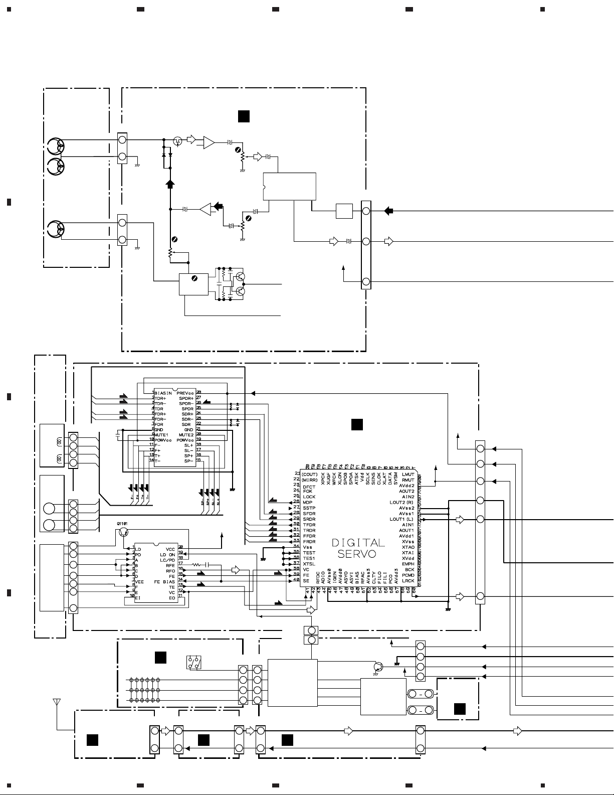
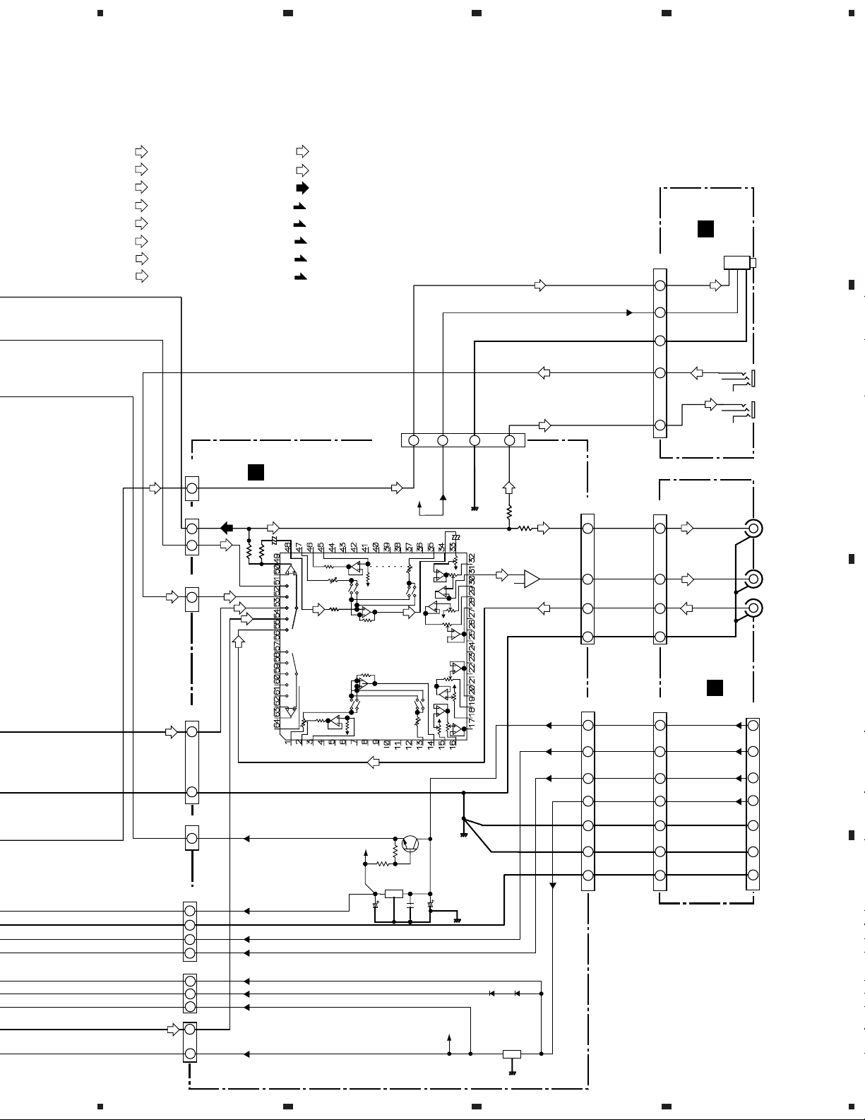
3. BLOCK DIAGRAM AND SCHEMATIC DIAGRAM
3.1 BLOCK DIAGRAM
A
MECHA ASSY
REC/PB
HEAD
ERASE
HEAD
CN2301
PB L
3
GND
2
CN2302
ERASE
1
GND
2
Q2301
(2SK373)
DS
G
(REC)
6
(NJM4558M)
PB
(BA4558MD)
+
VR2801
(BIAS)
5
L2801
BIAS OSC
B
(TS)
TFDR
(TS)
TRDR
(FS)
FFDR
(FS)
CN1101
T +
1
F -
2
F +
3
T -
4
CN1301
SL +
1
SL -
2
SP +
5
SP -
6
CN1101
LD ON
12
LD PD
9
PDIC PD1
7
PDIC PD2
6
F
15
E
8
VC
14
FRDR
(TS)
(TS)
IC1101
CXA1821M
IC1301
BA5970FP
(FS)
(FS)
FRONT PANEL
ASSY
K
KEY
(FS)
(TS)
JOG
CD MECHA ASSY
(2/2)
PICKUP ASSY
SL/SP
C
MOTOR
+
SL
-
+
SP
-
(1/2)
PICKUP ASSY
D
(TX)
TX CONNECT
7
2
TUNER MODULE
A
CN6201 CN161 J60
TX LcH
7
TX+5V
2
IC2301
3
+
2
-
IC2401
1
(SM)
(SM)
ASSY
B
DECK ASSY
+
1
VR2301
(PB LEVEL)
(REC)
3
2
+
1
3
(SM)
(CS)
(CS)
GNDCDM
V+5CD
CN150 CN50
JOG
KEY 1
KEY 2
KEY 3
TX LcH
TX+5V
J
(PB)
VR2401
(REC LEVEL)
Q2801
(2SC1815)
Q2802
(2SC1815)
TFDR
TRDR
FFDR
FRDR
10
10
17
17
13
13
15
15
J60
7
(TX)
2
+
3
IC2201
(HA1236AF)
DOLBY NR
8
REC OUT
+
(SM)
(CM)
(CM)
(TS)
(TS)
(FS)
(FS)
GND
(FS)
(TS)
44
38
PDG242A
SYSTEM U-COM
39
40
U-COM
ASSY
7
2
PB IN L
BIAS
Cro2
CD LD ON
CN10
CN10
IC5501
C
L2201
16
REC IN L
LINE OUT L
(PB)
V+12M
15
15
13
AC_PLUS
60
49
LCD_CE
LCD_CLK
48 8
LCD_DATA
50 9
LCD_POW
414
(TX) (TX)
J2201
MPX
5
+
4
7
CD ASSY
F
IC1201
CXD2587Q
GND
7
REC L
(REC)
PB L
(PB)
V+12M
V+12TX
Q5501
V+5.6U
IC5503
PDG243
LCD U-COM
GNDU
TX LcH
TX+5V
CN105
6
16
8
15
CN90
1 15
CN80
1 29
CN105
1
7
V+5CDM
V+5CD
V+5CD
D. OUT
V+12TX
GNDU
AC
V+5.6U
V+5UN
V+5CDM
GNDCDM
(CD)
(D.O)
GND
LCD
ASSY
D
V+5UN
V+5CD
CD L
D. OUT
J101
3
4
8
5
10
7
16
1234
Page 17
5
SIGNAL ROUTE
(CD)
: CD AUDIO SIGNAL
(L1)
: LINE 1 SIGNAL
(PB)
: DECK PB SIGNAL
(L2)
: LINE 2 SIGNAL
(MO)
: MAIN OUT SIGNAL
(D.O)
: OPTICAL OUT SIGNAL
(TX)
: TUNER AUDIO SIGNAL
(LO1)
: LINE OUT 1 SIGNAL
67
(LO2)
: LINE OUT 2 SIGNAL
(LO)
: LINE OUT SIGNAL
(REC)
: RECORDING SIGNAL
(FS)
: FOCUS SERVO LOOP LINE
(TS)
: TRACKING SERVO LOOP LINE
(SM)
: SPINDLE MOTOR ROUTE
(CM)
: CARRIAGE MOTOR ROUTE
(LM)
: LOADING MOTOR ROUTE
F- TERMINAL
ASSY
J103
(D.O) (D.O)
(L2)
V IN
VCC
GND OPT
LIN2
8
9
7
2
XC-IS21T
I
123
(L2)
8
A
OPT OUT
LINE IN2
(D.O)
(L2)
(CD)
(TX)
CN1
CN2
CN3
CN1
10
CN2
CN5
18
8
16
9
CN1
3
4
8
CN5
23
17
7
5
4
2
5
7
D. OUT
REC L
PB L
(PB)
LIN2
(L2)
CD L
GNDCDM
V+12M
V+12TX
GNDU
AC
V+5.6U
V+5UN
V+5CDM
V+5CD
TX LcH
TX+5V
(CD)
(REC)
(TX)
E
LIN 2
CD L
(L1)
(LO)
PB L
TX L
LIN1
AF ASSY
+
(MO)
CN3
(D.O)
IC3001
(LC75398NE)
(L1)
(2SD2395)
VDD
IC131
(NJM7812FA)
89 1
OPT IN/OUT
V+5
(MO)
Q2001
V+5 OPT
V+5
7
GND OPT
+
(MO)
LOUT2
(LO2)
IC3002
(NJM4558MD)
3
2
D3009D3008
IC141
(NJM7805FA)
(LO2)
LOUT2
CN32
LOUT1
(LO1)
+
AOUT L
1
-
12
LIN1
(L1) (L1)
GNDS
LOUT1
9
AOUT L
6
7
LIN1
GNDS
CN31
V+12UNV+12UN
9
AC
8
V+5.6V V+5.6V
7
V+5UN
10
B2GND
3
B1GND
2
GNDU
6
AC
V+5UN
B2GND
B1GND
GNDU
1
CN132
(LO1)
9
12
(MO)
6
7
R- TERMINAL
CN131
9
8
7
10
3
2
6
(LO2)
ASSY
H
CN7101
1
3
4
5
6
9
10
LINE OUT2
LINE OUT1
AUDIO OUT
LINE IN1
V+12UN
AC
V+5.6V
V+5UN
(M-IS21)
B2GND
TO. STEREO PWER AMPLIFIER
B1GND
GNDU
B
C
D
17
5
6
7
8
Page 18
1
234
XC-IS21T
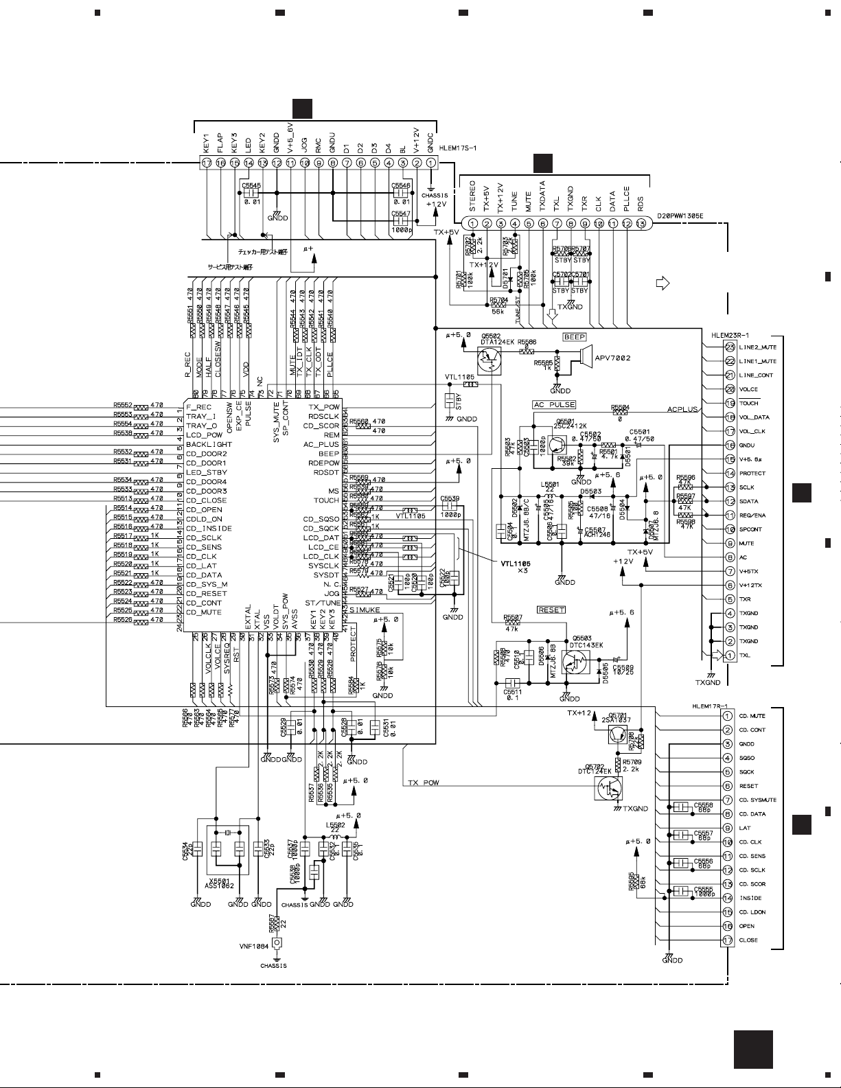
3.2 OVERALL CONNECTION DIAGRAM
A
CN1
B
J101
F
(AWU7305)
F-TERMINAL ASSY
I
E
CD ASSY
(AWU7311)
AF ASSY
(AWU7298)
CN1301
J111
J103
CN3
J107
CN7
CN11
G
CD MOTOR
ASSY
(AWU7318)
CN1101
CN6201
C
CN161
J60
J60
A
B
CN110
(AXQ7065)
(AWU7323)
FM/AM TUNER MODULE
D
CN190 CN180
TX CONNECT ASSY
D
CN10
LCD ASSY
(AWU7354)
U- COM ASSY
CN80CN90
C
(AWU7327)
18
1234
Page 19
5
67
8
XC-IS21T
Note : When ordering service parts, be sure to refer to "EXPLODED VIEWS and P AR TS LIST" or "PCB PARTS LIST".
To. OPTION DECK
CN132
CN32
CN5
CN105
C
CN7102 CN7101
R-TERMINAL ASSY
U- COM ASSY
(AWU7327)
H
(AWU7315)
To. STEREO POWER AMP (M-IS21)
CN131
CN2
CN31
CN20
J2201
CN2603
CN2701
J2202
J
(AWU7334)
DECK ASSY
A
B
FRONT PANEL ASSY
K
CN51
J51
L
LIGHT-L ASSY
(AWU7321)
(AWU7308)
CN50
CN150
J155
N
CD CLOSE SW ASSY
J55
(AWU7320)
M
CD OPEN SW ASSY
J54J154
(AWU7319)
CN2301
CN2302
C
D
19
5
6
7
8
Page 20
1
234
XC-IS21T
3.3 FM/AM TUNER MODULE and TX CONNECT ASSYS
A
RF AMP
(FM) (FM)
B
(FM) (FM)
(FM)
(FM)
1T378A
OSC
1T378A
(FM)
MIX AMP
(FM) (FM) (FM)
BUFFER
(FM)
IF AMP
FM +B SW
(FM)
(AM) (AM) (AM)
(FM)
(AM)
C
(AM)
MW RF TUNING BLOCK
AKX7041
(AM)
FM/AM TUNER MODULE
(AXQ7065)
D
: AM SIGNAL ROUTE
(FM)
: FM SIGNAL ROUTE
(TX)
: TUNER AUDIO SIGNAL
20
A
1234
Page 21
5
67
8
XC-IS21T
A
(AM)
(FM)
(AM)
(FM)
(FM)
AF AMP
(TX) (TX)
AF AMP
REGULATOR
(TX)
CN161 J60
CN6201
D20PYY1315
B
B
C
J60
C
(AWU7323)
PLL
TX CONNECT ASSY
D
21
5
6
7
A
B
8
Page 22
1
XC-IS21T
3.4 U-COM and LCD ASSYS
A
CN190 CN180
234
D
LCD ASSY
(AWU7354)
CN90
B
L5509 L5510
C
CN80
C
U-COM ASSY
(AWU7327)
D
CN20
J2202
J
22
C
D
1234
Page 23
5
67
8
XC-IS21T
K
CN150
IC5501
PDG242
CN50
B
J60
A
J60
5.6
SIGNAL ROUTE
(TX)
: TUNER AUDIO SIGNAL
(TX)
L5508
L5544
L5507
CN105
B
E
CN5
L5506
L5505
L5504
L5504 -L5506
LINE 2 MUTE
LINE CONT
LINE 1 MUTE
(TX)
C
CN10
F
CN110
D
23
5
6
7
C
8
Page 24

XC-IS21T
3.5 AF ASSY
A
1
234
CN7J107
B
J101
J2201
C
F
J
CN1
CN2
E
(PB)
(REC)
AF ASSY
(AWU7298)
(CD)
(TX)(TX)
(CD)
(L1)
(TX)
(REC)
(PB)
(L2)
(CD)
(TX)
(L1)
(PB)
(L2)
(LO)
(L2)
(LO)
(MO)
(L1)
(PB)
(REC)
(L1)(L1)
SIGNAL ROUTE
(CD)
: CD AUDIO SIGNAL
(L1)
: LINE 1 SIGNAL
(PB)
: DECK PB SIGNAL
(L2)
: LINE 2 SIGNAL
(MO)
: MAIN OUT SIGNAL
(TX)
: TUNER AUDIO SIGNAL
(LO1)
D
: LINE OUT 1 SIGNAL
(LO2)
: LINE OUT 2 SIGNAL
(LO)
: LINE OUT SIGNAL
(REC)
: RECORDING SIGNAL
24
E
(TX)
C
CN5
CN105
1234
Page 25

CN3
5
67
8
XC-IS21T
I
J103
(LO1)
(MO))
(LO)
(L2)
VTL1105
0
VTL1105
(L2)
(LO2)
0
(LO1)
A
CN31
H
CN131
100
(LO1)
(MO)(MO)(MO))
(LO1)
B
100
(L1)
S5688G
S5688G
(L1)(L1)
H
CN132
CN32
C
D
5
6
7
8
E
25
Page 26

1
234
XC-IS21T
3.6 CD and CD MOTOR ASSYS
A
(SM)
B
(FS)
(FS)
(TS)
(TS)
(SM)
(SM)
(CS)
(CS)
F
CD ASSY
(AWU7305)
(FS)
(SM)
(CM)
(CM)
(TS)
(TS)
(FS)
(FS)
C
To. P.U Assy
D
CN1301
To. CD MECHA
CN1101
(LM)
(LM)
(SM)
(SM)
(TS)
(FS)
(FS)
(TS)
Note: The encircled numbers denote measuring point in the schematic diagram.
IC1101- Pin 16:
1
PLAY MODE (RF)
H : 500nsec/div
1.0Vp-p
VC
IC1101- Pin 13 :
2
TEST MODE,
Tracking Open (TRER)
H : 5msec/div
VC : IC1101- Pin12
1.0Vp-p
VC
1
(FS)
2
(TS)
VC
(TS)
26
SIGNAL ROUTE
: CD AUDIO SIGNAL ROUTE
(FS)
: FOCUS SERVO LOOP LINE
(TS)
: TRACKING SERVO LOOP LINE
(SM)
: SPINDLE MOTOR ROUTE
(CM)
: CARRIAGE MOTOR ROUTE
(LM)
: LOADING MOTOR ROUTE
F
1234
Page 27

(SM)
(CM)
(CM)
(TS)
(TS)
(FS)
(FS)
5
67
8
XC-IS21T
A
J101
E
CN1
B
(FS)
(TS)
C
CN10
CN110
C
CD MOTOR ASSY
G
CN11J111
(AWU7318)
D
5
6
7
8
GF
27
Page 28

1
234
XC-IS21T
3.7 R-TERMINAL and F-TERMINAL ASSYS
A
H
CN7101
(AWU7315)
CN131
E
CN31
(M-IS21)
B
TO. STEREO POWER AMPLIFIER
R- TERMINAL ASSY
(L1)
VTL1096
VTL1096
(L1)
VTL1096
VTL1096
(MO)
(LO1)
(L1)
E
CN32
(LO1)
C
(MO) (MO)
D
VTL1096
CN7102
VTL1096
VTL1096
CN132
SIGNAL ROUTE
(MO)
: MAIN OUT SIGNAL
(L1)
: LINE 1 SIGNAL
(LO1)
: LINE OUT1 SIGNAL
To. OPTION DECK
28
H
1234
Page 29
1
F- TERMINAL ASSY
I
(AWU7311)
23
XC-IS21T
SIGNAL ROUTE
(L2)
: LINE2 SIGNAL
(LO2)
: LINE OUT2 SIGNA
4
A
B
(L2)
(L2)
(L2)(L2)
(LO2)
C
(LO2)
(LO2)
J103
D
E
CN3
29
1
2
3
I
4
Page 30
1
XC-IS21T
3.8 DECK ASSY
234
A
CN2301
CN2302
B
J
(PB)
(REC) (REC)
DECK ASSY
(AWU7334)
(PB)
(PB)
(PB)
(PB)
(REC)
(REC)
SIGNAL ROUTE
(PB)
: PB SIGNAL
(REC)
: RECORDING SIGNAL
C
D
30
J
1234
Page 31
5
67
8
XC-IS21T
A
X
J2201
(PB)
(REC)
(PB)
(REC)
(PB)
(PB)
(REC)
(PB)
E
CN2
(REC)
J2202
B
C
CN20
CN2603
5
C
CN2701
D
6
7
8
J
31
Page 32

1
234
XC-IS21T
3.9 FRONT PANEL, LIGHT-L, CD OPEN SW and CD CLOSE SW ASSYS
A
CN150
B
J51
CN51
C
CN50
L
LIGHT-L ASSY
(AWU7321)
DTA143EK-TLB
C
DTC124EK-TLB
SLR-343VC(NPQ)-TS
DTC124EK-TLB
K
FRONT PANEL ASSY
(AWU7308)
D
32
K
L
1234
Page 33

5
FRONT PANEL ASSY (SW name)
S5901: POWER (STANDBY/ON)
S5902: DISPLAY/RDS
S5903: TIMER REC/WAKE UP
S5904: TAPE/OPEN/CLOSE
S5905: TAPE
S5906: LINE1, 2
S5907: /TUNING+
S5908: REC/STOP
67
S5909: TREBLE
S5910: PLAY/PAUSE
S5911: ST.WIDE
S5912: BASS
S5913: STOP
S5914: BALANCE
S5915: TUNER
S5916: VOLUME/JOG
S5917: /TUNINGS5918: BALANCE
S5919: CD
S5920: STATION MEMORY
S5921: FREQ/STATION
S5922: REVERSE
S5923: DOLBY NR ON/OFF
8
XC-IS21T
A
B
C
J154
J54
M
CD OPEN SW ASSY
(AWU7319)
5
6
N
CD CLOSE SW ASSY
(AWU7320)
J155
J55
D
NM
7
8
33
Page 34

XC-IS21T
4. PCB CONNECTION DIAGRAM
NOTE FOR PCB DIAGRAMS :
1. Part numbers in PCB diagrams match those in the schematic
diagrams.
2. A comparison between the main parts of PCB and schematic
diagrams is shown below.
Symbol In PCB
Diagrams
BCE
BCE
D
Symbol In Schematic
Diagrams
BCEBCE
BCE
DGGSS
BCE
DGS
Part Name
Transistor
Transistor
with resistor
Field effect
transistor
Resistor array
3. The parts mounted on this PCB include all necessary parts for
several destinations.
For further information for respective destinations, be sure to
check with the schematic diagram.
4. View point of PCB diagrams.
Connector
Capacitor
SIDE A
P.C.Board
Chip Part
SIDE B
3-terminal
regulator
34
Page 35

1
234
4.1 FM/AM TUNER MODULE and TX CONNECT ASSY
C
B
TX CONNECT ASSY
XC-IS21T
J60
A
FM/AM TUNER MODULE
A
Q6204
(ANP7302-B)
Q6203
SIDE A
B
VR6201
FM/AM TUNER MODULE
A
IC6201
IC6202
Q6202Q6201
Q6205
Q6303 Q6302Q6301
Q6403
Q6404
B
TX CONNECT ASSY
Q6214
Q6402
Q6401
(ANP7159-B)
Q6304
Q6306
(ANP7302-B)
SIDE B
C
D
A
1
2
3
B
4
35
Page 36

1
XC-IS21T
4.2 U-COM and LCD ASSYS
D
A
B
LCD ASSY
C
U-COM ASSY
23
SIDE A
(ANP7301-B)
CN150
K
4
C
D
F
CN110
36
J2202
J
C
D
1234
B
J60
E
CN5
(ANP7302-B)
Page 37

1
U-COM ASSY
C
IC5501 IC5503 IC5502
Q5501 Q5502 Q5752 Q5702
Q5731 Q5511 Q5512
Q5503 Q5701
(ANP7302-B)
234
XC-IS21T
A
SIDE B
B
C
1
2
3
C
4
D
37
Page 38

1
23
XC-IS21T
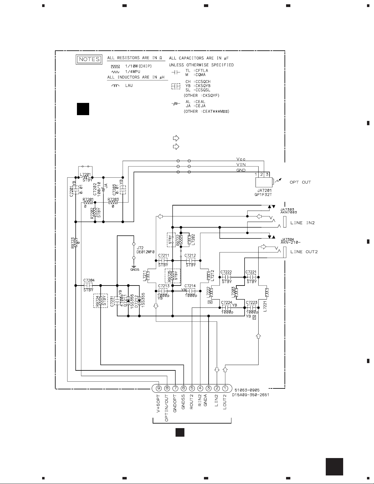
4.3 AF, F-TERMINAL and R-TERMINAL ASSYS
I
F-TERMINAL ASSY
A
J101
F
IC141 IC131 IC4001
E
AF ASSY
B
J
4
(ANP7301-B)
J2201
CD TOUCH
SW
C
(ANP7301-B)
C
CN105
H
R-TERMINAL ASSY
D
SIDE A
(ANP7301-B)
38
E
H
1234
I
Page 39

E
AF ASSY
1
234
XC-IS21T
I
F-TERMINAL ASSY
(ANP7301-B)
A
B
IC7301 IC3002 Q3005
H
R-TERMINAL ASSY
Q3011 Q3001 Q3002 Q3003 Q3013 Q3010
SIDE B
(ANP7301-B)
1
Q3006 Q3004 Q3009 Q3015 Q3014
E
2
3
H
(ANP7301-B)
I
4
C
D
39
Page 40

1
XC-IS21T
4.4 CD and CD MOTOR ASSYS
A
SIDE A
23
G
CD MOTOR
ASSY
4
F
CD ASSY
CN1
CD MECHA
B
C
E
(ANP7301-B)
(ANP7301-B)
Q7005- Q7008
D
40
F
G
1234
Q1101
C
CN10CD MECHA
Page 41
1
234
XC-IS21T
SIDE B
F
CD ASSY
Q1403 Q1404 Q1402 Q1401 Q7002 Q7003
Q7004
Q7001Q1202IC1201 IC1301
A
B
C
(ANP7301-B)
D
F
1
2
3
4
41
Page 42

1
XC-IS21T
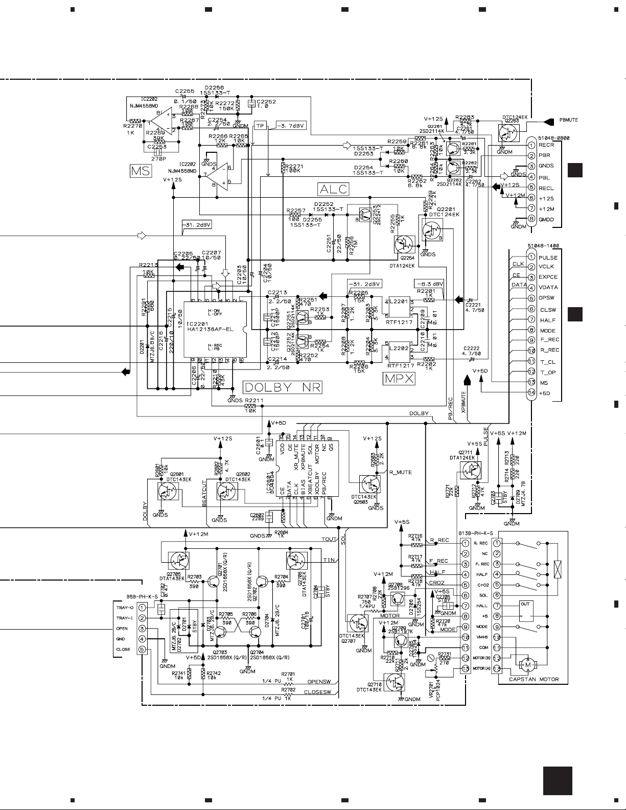
4.5 DECK ASSY
A
J
DECK ASSY
CN2
E
B
23
DECK MECHA
4
(ANP7302-B)
C
C
CN20
Q2702
Q2704 Q2703
Q2701 Q2708
DECK MECHA
Q2805 Q2301
Q2801 Q2802 Q2803 Q2806 Q2802
DECK MECHADECK MECHA
VR2401VR2802VR2801VR2701 VR2402
VR2302
SIDE A
D
42
J
1234
Page 43
J
DECK ASSY
1
234
XC-IS21T
A
B
Q2305
IC2301 Q2303
Q2306 Q2304
Q2401
Q2402
Q2452
1
Q2351 Q2201 Q2252 Q2602 Q2603
Q2254 Q2253 Q2251 Q2262 Q2261 Q2263Q2451 IC2401 IC2201
IC2202
Q2707
Q2710 Q2706Q2711
SIDE B
2
3
Q2709 Q2705
IC2601
(ANP7302-B)
J
4
C
D
43
Page 44

1
23
XC-IS21T
4.6 FRONT PANEL, LIGHT-L, CD CLOSE SW and CD OPEN SW ASSYS
K
FRONT PANEL ASSY
A
M
CD OPEN SW ASSY
N
CD CLOSE SW ASSY
B
4
(ANP7301-B)
C
L
LIGHT-L ASSY
(ANP7301-B)
C
(ANP7301-B)
CN50
D
(ANP7301-B)
SIDE A
44
K
L
1234
M
N
Page 45
1
234
XC-IS21T
K
FRONT PANEL ASSY
A
B
Q5902
Q5901
Q5903
C
D
(ANP7301-B)
SIDE B
K
1
2
3
4
45
Page 46

XC-IS21T
5. PCB PARTS LIST
NOTES:•Parts marked by "NSP" are generally unavailable because they are not in our Master Spare Parts List.
The mark found on some component parts indicates the importance of the safety factor of the part.
•
Therefore, when replacing, be sure to use parts of identical designation.
When ordering resistors, first convert resistance values into code form as shown in the following examples.
•
Ex.1 When there are 2 effective digits (any digit apart from 0), such as 560 ohm and 47k ohm (tolerance is shown by J=5%,
and K=10%).
560 Ω→56 × 10
47k Ω→47 × 103→ 473 ........................................................RD1/4PU 4 7 3 J
0.5 Ω→R50 .....................................................................................RN2H
1 Ω→1R0 .....................................................................................RS1P
Ex.2 When there are 3 effective digits (such as in high precision metal film resistors).
5.62k Ω→ 562 × 10
1
→ 561 ........................................................RD1/4PU 5 6 1 J
R 5 0
1 R 0
1
→ 5621 ......................................................RN1/4PC 5 6 2 1 F
K
K
Mark No. Description Part No.
LIST OF ASSEMBLIES
FM/AM TUNER MODULE AXQ7065
NSP COMPLEX ASSY AWM7433
NSP CD OPEN SW ASSY AWU7319
NSP CD CLOSE SW ASSY AWU7320
NSP LIGHT-L ASSY AWU7321
NSP LCD ASSY AWU7354
NSP DECK-COMP ASSY AWM7441
NSP TX CONNECT ASSY AWU7323
A
SEMICONDUCTORS
COILS AND FILTERS
AF ASSY AWU7298
CD ASSY AWU7305
FRONT PANEL ASSY AWU7308
F-TERMINAL ASSY AWU7311
R-TERMINAL ASSY AWU7315
CD MOTOR ASSY AWU7318
U-COM ASSY AWU7327
DECK ASSY AWU7334
FM/AM TUNER MODULE
IC6201 LA1832ML
IC6202 LC72131MD
Q6402 2SC2223
Q6203 2SC2705
Q6201, Q6202 2SC2712
Q6214, Q6403 2SC2714
Q6404 2SK302
Q6401 3SK194
Q6204 DTA124ES
Q6205 DTC124EK
D6202 1SS254
D6401, D6402 1T378A
L6404 ATC1003
L6401 ATC1020
L6402 ATC1021
F6204 ATF-107
F6203 ATF-119
F6401 ATF-155
F6206 ATF7008
F6202 ATF7011
L6206, L6208, L6403 LAU2R2J
Mark No. Description Part No.
TRANSFORMERS
T6201 ATB7008
T6401 ATE7002
CAPACITORS
C6208 CCSQCH100D50
C6212, C6274, C6275, C6408 CCSQCH101J50
C6412 CCSQCH102J50
C6221, C6222, C6416 CCSQCH150J50
C6271 CCSQCH200J50
C6415 CCSQCH330J50
C6406 CCSQCH331J50
C6401, C6419 CCSQCH5R0C50
C6407 CCSQCK1R0C50
C6410 CCSQCK2R0C50
C6413 CCSQRH180J50
C6414 CCSQRH8R0D50
C6405 CCSQTH150J50
C6234, C6235 CEAL1R0M50
C6245 CEAL470M16
C6224 CEAT100M50
C6243 CEAT101M16
C6231 CEAT1R0M50
C6227 CEAT220M25
C6214, C6236 CEAT2R2M50
C6262 CEAT3R3M50
C6219 CEAT470M10
C6244 CEAT470M16
C6249, C6250, C6265, C6266 CEAT4R7M50
C6258 CEJA470M16
C6215 CFTLA103J50
C6211, C6254, C6403, C6417 CKSQYB102K50
C6201, C6205, C6210, C6237, C6276 CKSQYB103K50
C6278, C6280, C6281, C6402, C6409 CKSQYB103K50
C6418 CKSQYB103K50
C6251, C6252 CKSQYB153K50
C6203, C6259 CKSQYB223K50
C6228 CKSQYB472K50
C6209 CKSQYB473K50
C6230 CKSQYB821K50
C6218, C6223, C6255 CKSQYF103Z50
C6220, C6226, C6242, C6256 CKSQYF223Z50
C6225 CKSQYF473Z50
46
Page 47

XC-IS21T
Mark No. Description Part No.
RESISTORS
R6280 RD1/4PU101J
R6413, R6416, R6418, R6906, R6909 RS1/8S0R0J
R6401 RS1/8S470J
VR6201 (10kΩ) PCP1029
Other Resistors RS1/10S&&& J
OTHERS
BN6202 (4P ANTENA TERMINAL) AKE7051
X6202 (456 kHz) ASS1066
X6201 (7.2000 MHz) ASS1093
CN6201 (14P SOCKET) KP200IA14L
AF ASSY
E
SEMICONDUCTORS
IC3001 LC75396NE
IC7301 NJM062M
IC3002 NJM4558MD
IC141 NJM7805FA
IC131 NJM7812FA
Q3004 2SC2412K
Q3001, Q3002, Q3005, Q3006 2SD2114K
Q3009, Q3010 2SD2114K
Q2001 2SD2395
Q3003 DTA124EK
Q3011, Q3013, Q3015 DTA143EK
Q7301 DTC114EK
Q3014 DTC124EK
D3006, D3007, D7301–D7304 1SS133
D3011, D3016 1SS355
D3004 MTZJ11C
D3008, D3009 S5688G
COILS AND FILTERS
L7301 LAU220J
L3110 VTL1096
L3101, L3103 VTL1105
CAPACITORS
C3039, C3040, C3057–C3059 CCSQCH101J50
C3203, C3204, C3207, C3208 CCSQCH101J50
C3205, C3206 CCSQCH271J50
C3011, C3012, C3025, C3026 CEAT100M50
C3029, C3030 CEAT100M50
C131, C141, C3041, C3042 CEAT1R0M50
C3031 CEAT220M50
C3001–C3008, C3013, C3014 CEAT2R2M50
C3023, C3024, C3035, C3036 CEAT2R2M50
C3055, C3056 CEAT2R2M50
C133, C143, C3096, C7302 CEAT470M16
C7304 CEJA4R7M50
C3015, C3016 CFTYA474J50
C3110, C3202 CKSQYB103K50
C7301 CKSQYB221K50
C3121–C3123 CKSQYB223K50
C3047, C3048 CKSQYB473K50
C3019, C3020 CKSQYB562K50
C3021, C3022 CKSQYB681K50
C3032 CKSQYB682K50
Mark No. Description Part No.
C132, C142, C3017, C3018, C3044 CKSQYF104Z50
C3099, C7305 CKSQYF104Z50
C3045, C3046 CKSQYF684Z16
RESISTORS
R2002 RD1/4PMF100J
Other Resistors RS1/10S&&& J
OTHERS
CN5 (23P FFC CONNECTOR) 52045-2345
CN2 (8P JUMPER CONNECTOR) 52147-0810
CN1 (12P JUMPER CONNECTOR) 52147-1210
CN7 (3P CONNECTOR) B3B-PH-K-S
CN31 (10P PLUG) KM200IB10
CN32 (12P PLUG) KM200IB12
CN3 (9P JUMPER CONNECTOR) KPE9
CD ASSY
F
SEMICONDUCTORS
IC1301 BA5970FP
IC1101 CXA1821M
IC1201 CXD2587Q
Q7002, Q7004 2SA1037K
Q1101 2SA854S
Q7005–Q7008 2SD1858X
Q1401, Q1402 2SD2114K
Q1201, Q1403, Q1404 DTA124EK
Q1202 DTC114TK
Q7001, Q7003 DTC124EK
D1101, D1202, D7003–D7006 1SS133
D1201 1SS85
D1401, D1402 DAN202K
D7002 MTZJ3.6B
D7001 MTZJ6.2C
COILS AND FILTERS
L1101, L1102, L1201, L1231, L1232 LAU100J
L1401, L1601 LAU100J
L7001 LFA100J
L1402, L1602 VTL1105
CAPACITORS
C1201, C1202 CCSQCH150J50
C1401, C1402 CCSQCH151J50
C1107 CCSQCH220J50
C1239, C1246, C1247 CCSQCH221J50
C1604 CCSQCH270J50
C1280 CCSQCH331J50
C1322, C1324 CCSQCH681J50
C1403, C1404 CCSQSL681J50
C1102, C1104, C1203, C1233, C1240 CEJA101M10
C1242, C1249, C1411, C1602 CEJA101M10
C1301, C1307, C1308, C7003 CEJA101M16
C1405, C1406 CEJA2R2M50
C1109, C1110 CEJA330M25
C1238 CEJAR47M50
C1331 CKSQYB102K50
47
Page 48

XC-IS21T
Mark No. Description Part No.
C1204–C1206, C1237, C1253, C1271 CKSQYB103K50
C1416, C1605 CKSQYB103K50
C1245 CKSQYB104K25
C1236 CKSQYB152K50
C1231 CKSQYB332K50
C1341, C1342 CKSQYB333K50
C1235, C1321, C1323 CKSQYB473K50
C1311, C1312 CKSQYB681K50
C1332 CKSQYB682K50
C1101, C1103, C1108, C1111, C1232 CKSQYF103Z50
C1234, C1241, C1250, C1251, C1276 CKSQYF103Z50
C1302–C1306, C1413, C1414, C1417 CKSQYF103Z50
C1601, C1603 CKSQYF103Z50
C7001, C7002 CKSQYF104Z50
RESISTORS
R7003 RD1/4PU181J
R7007 RD1/4PU221J
R7006 RD1/4PU331J
R7005 RD1/4PU470J
Other Resistors RS1/10S&&& J
OTHERS
111 (3P CABLE HOLDER) 51048-0300
101 (12P CABLE HOLDER) 51048-1200
CN110 (17P FFC CONNECTOR) 52044-1745
CN1101 (16P FFC CONNECTOR) 52089-1620
J111 (3P FLAT CABLE) D20PYY0310E
Mark No. Description Part No.
F-TERMINAL ASSY
I
SEMICONDUCTORS
D7211, D7212 1SS355
COILS AND FILTERS
L7202, L7203, L7211, L7212 VTL1096
L7221, L7222 VTL1096
CAPACITORS
C7202 CEJA101M10
C7213, C7214, C7223, C7224 CKSQYB102K50
C7201, C7203 CKSQYB103K50
C7231 CKSQYB472K50
RESISTORS
Other Resistors RS1/10S&&& J
OTHERS
103 (9P CABLE HOLDER) 51063-0905
7304 (MINE JACK) AKN-210
7303 (MINI JACK) AKN7003
J103 (JUMPER WIRE) D15A09-350-2651
JA7201 (OPTICAL LINK OUT) GP1F32T
R-TERMINAL ASSY
H
COILS AND FILTERS
L7101–L7106, L7111 VTL1096
J101 (12P FLAT CABLE) D20PYY1215E
CN1301 (6P CONNECTOR) S6B-ZR
1001, 1002 (PCB BINDER) VEF1040
X1201 (16.9344MHz) PSS1008
FRONT PANEL ASSY
K
SEMICONDUCTORS
Q5901 DTA143EK
Q5902, Q5903 DTC124EK
D5902, D5903 1SS133
D5908 1SS355
D5901 MTZJ5.6B
D5907 SLR-343VC
SWITCHES AND RELAYS
S5916 ASX7026
S5901–S5915, S5917–S5923 XSG3001
CAPACITORS
C5902 CEJA101M10
C5903 CKSQYF103Z50
RESISTORS
R5917 RD1/2PM471J
R5909 RD1/2PM820J
Other Resistors RS1/10S&&& J
OTHERS
154, 155 (3P CABLE HOLDER) 51048-0300
CN150 (17P FFC CONNECTOR) 52044-1745
CN51 (3P JUMPER CONNECTOR) 52147-0310
J54 (3P FLAT CABLE) D20PYY0310E
J55 (3P FLAT CABLE) D20PYY0330E
CAPACITORS
C7102, C7104 CCSQCH221J50
C7154 CKSQYB102K50
C7131 CKSQYB103K50
RESISTORS
Other Resistors RS1/10S&&& J
OTHERS
JA7105 (2P PIN JACK) AKB7043
CN7104 (4P PIN JACK) AKB7114
CN7102 (5P SOCKET) AKP7042
CN7101 (10P SOCKET) AKP7048
CN131 (10P SOCKET) KP200IB10L
CN132 (12P SOCKET) KP200IB12L
CD MOTOR ASSY
G
CAPACITORS
C7501 CKSQYF104Z50
OTHERS
CN11 (3P JUMPER CONNECTOR) 52151-0310
CD OPEN SW ASSY
M
SWITCHES AND RELAYS
S7401, S7402 VSH1019
OTHERS
54 (3P CABLE HOLDER) 51048-0300
5901 (REMOTE RECEIVER UNIT) GP1U27X
48
Page 49

XC-IS21T
Mark No. Description Part No.
CD CLOSE SW ASSY
N
SWITCHES AND RELAYS
S7403, S7404 ASG7015
OTHERS
55 (3P CABLE HOLDER) 51048-0300
LIGHT-L ASSY
L
SEMICONDUCTORS
D5971 NSPBF50S-8451
OTHERS
51 (3P CABLE HOLDER) 51048-0300
J51 (3P CABLE HOLDER) D20PYY0310E
LCD ASSY
D
OTHERS
CN190 (15P FFC CONNECTOR) 52045-1545
CN180 (29P FFC CONNECTOR) 52045-2945
V5501 (LCD DISPLAY) AAV7066
TX CONNECT ASSY
B
CAPACITORS
C9999 CKSQYB104K25
OTHERS
160 (13P CABLE HOLDER) 51048-1300
CN161 (14P CONNECTOR) 9176B-14L
U-COM ASSY
C
SEMICONDUCTORS
IC5501 PDG242B
IC5503 PDG243A
Q5701 2SA1037K
Q5501 2SC2412K
Q5502 DTA124EK
Q5702 DTC124EK
Q5503, Q5511, Q5512 DTC143EK
D5501, D5503–D5505, D5701 1SS133
D5502, D5506, D5507 MTZJ6.8B
COILS AND FILTERS
L5501, L5502, L5509, L5510 LAU220J
L5503–L5508 VTL1105
Mark No. Description Part No.
C5528, C5529, C5531, C5545, C5546 CKSQYB103K50
C5524–C5526 CKSQYB104K25
C5504, C5506, C5510, C5511, C5523 CKSQYF104Z50
C5532, C5535, C5536, C5542 CKSQYF104Z50
RESISTORS
R5577–R5580 RD1/4PU471J
Other Resistors RS1/10S&&& J
OTHERS
60 (13P CABLE HOLDER) 51048-1300
CN10 (17P FFC CONNECTOR) 52044-1745
CN105 (23P FFC CONNECTOR) 52044-2345
CN90 (15P FFC CONNECTOR) 52045-1545
CN50 (17P FFC CONNECTOR) 52045-1745
X5501 (12MHz) ASS1062
X5502 (10MHz) DSS1048
CN80 (29P FFC CONNECTOR) 52045-2945
CN20 (14P JUMPER CONNECTOR) 52147-1410
(BUZZER) APV7002
J60 (13P FLAT CABLE) D20PYY1315E
10, 20 (PCB BINDER) VEF1040
KN5501 (EARTH METAL FITTING) VNF1084
DECK ASSY
J
SEMICONDUCTORS
IC2601 BU4094BCF
IC2201 HA12136AF
IC2202,IC2301,IC2401 NJM4558MD
Q2709 2SB1197K
Q2803 2SB1238X
Q2708 2SB1296
Q2801, Q2802, Q2805 2SC1815
Q2806 2SC2240
Q2253 2SC2412K
Q2701–Q2704 2SD1858X
Q2251, Q2252, Q2261, Q2262 2SD2114K
Q2451, Q2452 2SD2114K
Q2301, Q2302 2SK373
Q2254, Q2711 DTA124EK
Q2705, Q2706 DTA143EK
Q2303–Q2306, Q2401, Q2402 DTC114TK
Q2201, Q2263, Q2351, Q2804 DTC124EK
Q2601–Q2603, Q2707, Q2710 DTC143EK
D2252–D2256, D2301–D2306, D2311 1SS133
D2421, D2705, D2706 1SS133
CAPACITORS
C5507 (0.047F/5.5V) ACH1246
C5520–C5522 CCSQCH101J50
C5533, C5534 CCSQCH220J50
C5556–C5558 CCSQCH680J50
C5509 CEAT100M50
C5502 CEAT1R0M50
C5505, C5508 CEAT470M16
C5501 CEATR47M50
C5503, C5537–C5539, C5541, C5547 CKSQYB102K50
C5555 CKSQYB102K50
D2709 MTZJ4.7B
D2201, D2703, D2704 MTZJ6.2B
COILS AND FILTERS
L2802 LFA121J
L2801 RTD1082
L2401, L2402 RTF1004
L2403, L2404 RTF1021
F2201, F2202 RTF1217
L2501, L2502 VTL1096
49
Page 50

XC-IS21T
Mark No. Description Part No.
CAPACITORS
C2809 CCCSL151K2H
C2301, C2302 CCSQCH100D50
C2423, C2424 CCSQCH221J50
C2253 CCSQCH271J50
C2303, C2304 CCSQCH681J50
C2203, C2204, C2207, C2215 CEAT100M50
C2311, C2312, C2407, C2408 CEAT100M50
C2701 CEAT101M16
C2201, C2202, C2217, C2218, C2255 CEAT1R0M50
C2403, C2404 CEAT1R0M50
C2251 CEAT220M50
C2216 CEAT221M10
C2213, C2214, C2254 CEAT2R2M50
C2309, C2310, C2805, C2806, C2810 CEAT330M16
C2314, C2425, C2807 CEAT470M16
C2221, C2222, C2261, C2262 CEAT4R7M50
C2419, C2420 CEAT4R7M50
C2205, C2206 CEATR22M50
C2501, C2502 CKSQYB102K50
C2601 CKSQYB104K25
C2252 CKSQYB105K10
C2411, C2412 CKSQYB122K50
C2211, C2212, C2421, C2422 CKSQYB152K50
C2602 CKSQYB221K50
C2401, C2402 CKSQYB332K50
C2451 CKSQYB473K50
C2702 CKSQYB474K16
C2808 CQHA822J2A
C2209, C2210 CQMA103J50
C2801 CQMA123J50
C2409, C2410 CQMA223J50
C2803, C2804 CQMA332J50
C2417, C2418 CQMA393J50
C2307, C2308, C2802 CQMA682J50
C2405, C2406 CQMA683J50
RESISTORS
R2805 RD1/2PM161J
R2806 RD1/2PM201J
R2703–R2706 RD1/2PM391J
R2803 RD1/2PM4R7J
R2701, R2702 RD1/4PU102J
R2707 RD1/4PU751J
VR2701 (1kΩ) PCP1024
VR2301,VR2302 (4.7kΩ) PCP1028
VR2401,VR2402 (22kΩ) PCP1030
VR2801,VR2802 (100kΩ) PCP1032
Other Resistors RS1/10S&&& J
OTHERS
102 (8P CABLE HOLDER) 51048-0800
CN2701 (13P CONNECTOR) B13B-PH-K-S
CN2302 (2P CONNECTOR) B2B-PH-K-S
CN2301 (4P CONNECTOR) B4B-PH-K-S
CN2603 (5P CONNECTOR) B5B-PH-K-S
J2201 (8P FLAT CABLE) D20PYY0825E
J2202 (14P FLAT CABLE) D20PYY1425E
(BINDER) VEF1040
50
Page 51

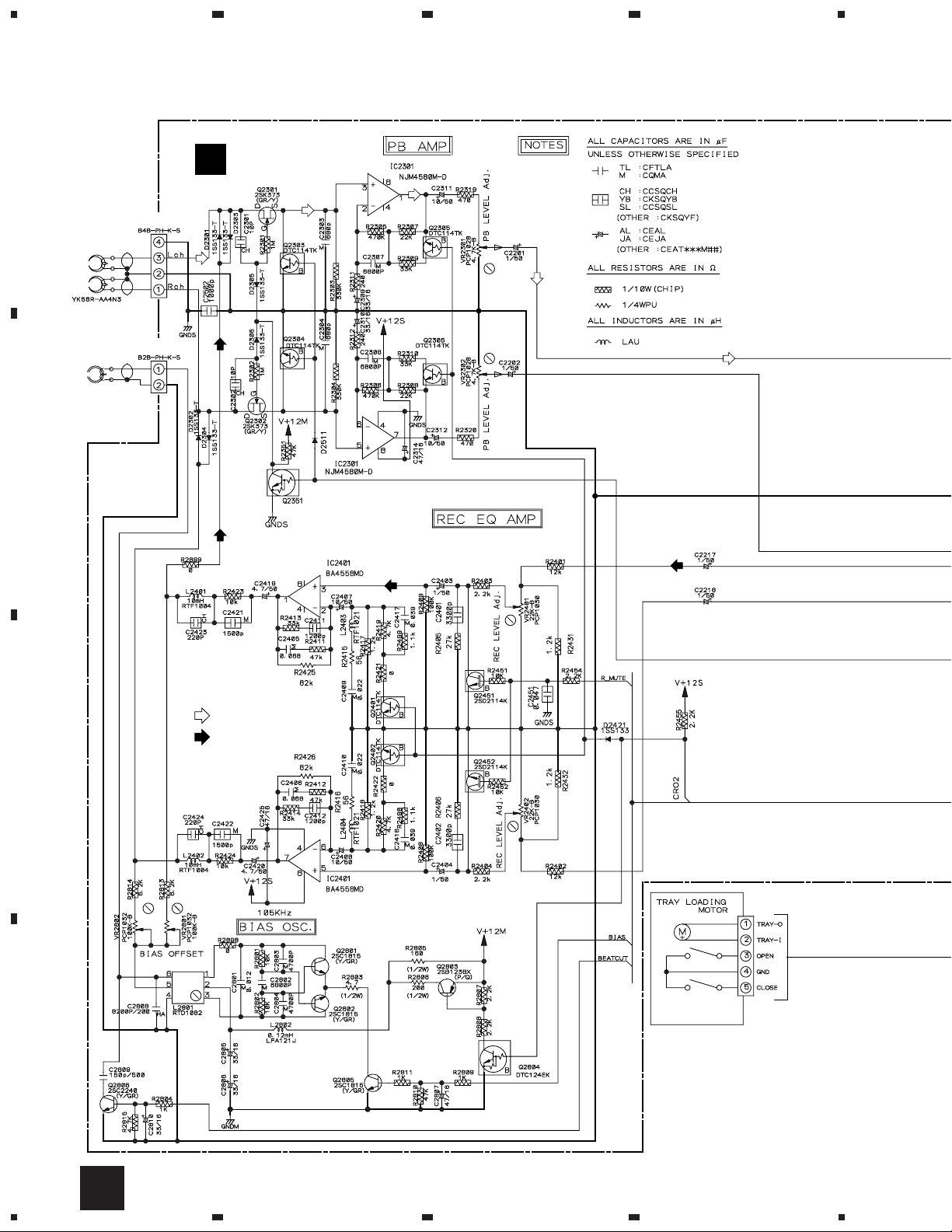
6. ADJUSTMENT
For adjustment, use the stereo power amplifier (M-IS21).
6.1 DECK SECTION
6.1.1 Adjustment Condition
(1) The ground at the time of adjustment shall be W166.
(Refer to Fig. 6–3).
(2) Clean the heads and demagnetize them using a head eraser.
(3) Set the measurement level to 0 dBV = 1 Vrms.
(4) Use the specified tape for adjustment. Use the labeled (A) side
of the test tape.
NCT–111 : For Tape Speed adjustment
STD-331E : For Playback adjustment
STD–632 : Normal blank tape
* As the reference recording level is 250 nwb/m for STD–
331E, the recording level will be higher by 4 dB for STD–
331B (160nwb/m). When adjusting, pay carefull attention
to the type of tape used.
(5) Provide yourself with the following measuring devides:
÷ AC millivoltmeter
÷ Low-frequency oscillator
÷ Attenuator
÷ Oscilloscope
(6) Adjust both right and left channels unless otherwise specified.
(7) Turn the DOLBY NR switch off unless otherwize specified.
(8) Warm up the unit for several minutes before adjustment. In
particular, be sure to warm up the unit in the REC/PLAY mode
for 3 to 5 minutes before starting recording/playback frequency
characteristics adjustment.
(9) Always follow the indicated adjustment order.
Otherwise, a complete adjustment may not be achieved.
7 List of Adjustments
¶ Playback Section
(1) Tape Speed Confirmation
(2) Head Azimuth Adjustment
(3) Playback Level Adjustment
¶ Recording Section
(1) Recording Bias Adjustment
(2) Recording Level Adjustment
PLAY BACK
250
3dB
RECORDING
250
3dB
10k
3dB 4dB
10k
3dB
XC-IS21T
12.5k
12.5k
5dB
0 dB
30s
315 Hz
Fig. 6-1 Frequency Characteristics
Dolby noise reduction manufactured under license from Dolby
Laboratories Licensing Corporation.
“DOLBY” and the double-D symbol are trademarks of Dolby
Laboratories Licensing Corporation.
0 dB: 315 Hz, 250 nwb/m
30 s 30 s 30 s 10s 10s .......................................................................................................... 10s
6.3 kHz 10 kHz 315 Hz 14 kHz
12.5
kHz
10 kHz
6.3
8 kHz 4 kHz 2 kHz
kHz
1 kHz
500Hz250Hz125
Hz
63 Hz 40 Hz
Fig. 6-2 Test Tape STD– 331E
–20 dB
51
Page 52

XC-IS21T
6.1.2 Playback Section
(1) Tape Speed Confirmation
No. Mode Input Signal/Test Tape Adjustment Points Measurement Points Adjustment Value Remarks
PLAY1
NCT-111 (3 kHz)
VR2701 (DECK ASSY)
(Refer to Fig. 6-3)
TP R (C2204)
(DECK ASSY)
(2) Head Azimuth Adjustment
¶ This unit is equipped with auto tape selector.
¶ Do not switch between forward and reverse operation with the screwdriver inserted.
No. Mode Input Signal/Test Tape Adjustment Points
Measurement
Points
3000 Hz Hz
Adjustment
Value
+10
–10
FWD adjustment
REV Confirmation
( 3000 Hz Hz )
Remarks
+60
–60
PLAY1
STD-331E test tape
(Playback: 10 kHz, –20 dB)
Head azimuth
adjustment Screw
(Refer to Fig. 6-3)
TP L (C2203)
TP R (C2204)
(DECK ASSY)
Max. Playback
signal level
(3) Playback Level Adjustment
¶ Since this adjustment determines playback DolbyNR level, Perform it carefully.
Measurement
Points
1
PLAY
STD-331E test tape
(Playback: 315 Hz, 0 dB)
L ch
R ch VR2302
VR2301
TP L (C2203)
TP R (C2204)
(DECK ASSY)
Adjustment
Value
–3.7 dBV
6.1.3 Recording Section
(1) Recording Bias Adjustment
¶ After the adjustment, caution should be exercised so as not to become under bias by checking the distortion rate.
No. Mode Input Signal/Test Tape Adjustment Points
REC/
1
PAUSE
REC =
2
PLAY
Input a 315Hz signal to the LINE -
IN terminal. ∗
Load the STD–632 test tape and
record/playback the 315Hz and
10kHz signals. (see the Note below)
Input signal level –23.7 dBV
L ch
R ch VR2802
VR2801
Measurement
Points
TP L (C2203)
TP R (C2204)
(DECK ASSY)
Adjustment
Value
Repeat adjustment until playback level of
the 10kHz signal is within 0.5dBV ±0.5dB
from that of the 315Hz signal.
After adjustment, apply silicon
bond to the head azimuth
adjustment screw.
RemarksNo. Mode Input Signal/Test Tape Adjustment Points
Remarks
Note: Set the 10kHz input signal level to the same value as the 315Hz input signal level of step 1.
(2) Recording Level Adjustment
No. Mode Input Signal/Test Tape Adjustment Points
REC/
1
PAUSE
REC =
2
PLAY
Input a 315Hz signal to the LINE-
IN terminal.∗
STD–632 test tape and record/
playback the 315Hz signal.
Input signal level –7.7 dBV
L ch
R ch VR2402
VR2401
52
Measurement
Points
TP L (C2203)
TP R (C2204)
(DECK ASSY)
Adjustment
Value
Repeat recording, playback and
adjustment until playback level of the
315Hz signal becomes –
Remarks
7.7dBV±0.5dB
.
Page 53

XC-IS21T
DECK ASSY
J
SIDE A
W166
(TP GND)
C2203
(TP Lch)
VR2301
(Lch)
PB LEVEL
C2204
(TP Rch)
VR2302
(Rch)
VR2701
MECHANISM UNIT
VR2801
(Lch)
FWD Azimuth
Adjustment Screw
BIAS TAPE SPEED
VR2802
(Rch)
REV Azimuth
Adjustment Screw
VR2401
(Lch)
REC LEVEL
VR2402
(Rch)
Fig. 6-3 Adjustment and Measurement Points
53
Page 54

XC-IS21T
6.2 CD SECTION
Note : There is no information to be shown in this CD adjustment.
6.2.1 HOW TO START / CANCEL TEST MODE
TEST MODE : ON
TEST MODE
W302
Short circuit
W301
U-COM ASSY
C
U-COM ASSY
SIDE A
W302
W301
U-COM ASSY
Release
Short point
TEST MODE
W302
W301
TX
TEST
MODE
CD
CD
TEST
MODE
2
TEST MODE : STOP → CANCEL
STOP
All Operations
54
Fig. 6-4
Front
Page 55
FUNCTION OF CD TEST MODE
Carriage IN
DISPLAY
Laser diode: LIGHT UP
Focus servo: ON
XC-IS21T
OPEN/CLOSE
CD cover
Open / Close
Carriage OUT
TEST MODE : PLAY
TEST DISC: YEDS-7
FL DISPLAY
[ : ]
STOP
DISPLAY
Laser diode: LIGHT UP
Focus servo: CLOSE
FL DISPLAY
[FOCUS ON]
22
Spindle motor: START
Spindle servo: CLOSE
[SPNDL KICK] → [SERVO ON]
Auto-matic adjustment
Average proccesing
FL DISPLAY
Spindle kick,
Tracking servo,
Slider servo: ON/OFF
A
A
CLOSE
Tracking servo:
FL DISPLAY
[SERVO ON]
OPEN
FL DISPLAY
[SERVO OFF]
inwards
Pickup Move
FL DISPLAY
[XX : XX] → [SERVO OFF]
outwards
55
Page 56
XC-IS21T
6.3 TUNER SECTION
6.3.1 FM TUNER SECTION
Set the mode selector to FM BAND.
Connect the wiring as shown in Fig. 6-5.
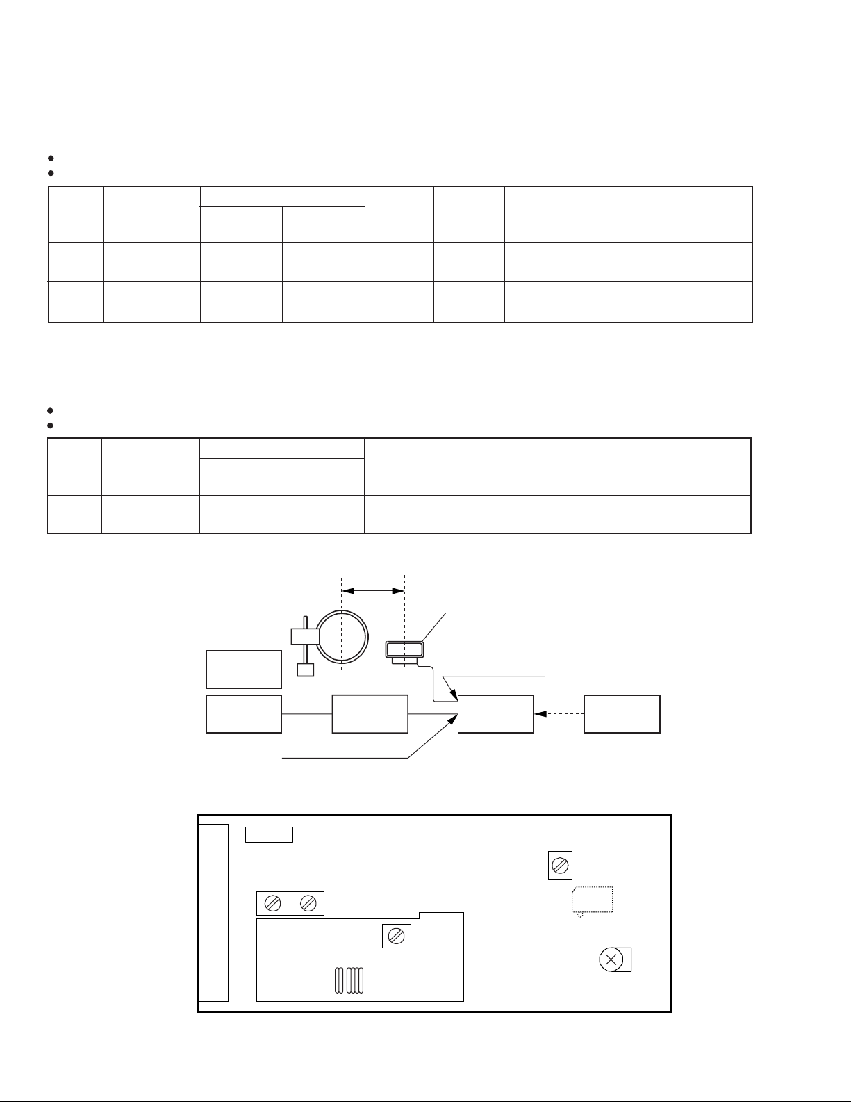
Step No.
1
2
Adjustment
Title
Front End
Sensitivity
TUNED IND.
Lighting Level
FM SG (1kHz, ±75kHz dev.)
Frequency
(MHz)
98
Level
(dBµV)
0 – 30 98MHz
98
Reception
Frequency
Display
98 MHz18 ± 2
Adjustment
Location
L6402
T6401
VR6201
Specifications
Adjust so that the DC voltage between the IC6201Pin 20 and GND becomes at maximum level.
Adjust so that the indicator of TUNED IND. starts
to light up.
Note: Before adjusting, make sure there is no gap between L6101 and L6102 . If there is a gap between them, bring them into contact with
each other first, and then make adjustments.
6.3.2 AM TUNER SECTION
Set the mode selector to AM BAND.
Connect the wiring as shown in Fig. 6-5
AM SG (400Hz, 30% Mod.)
Frequency
(kHz)
1
999*
Level
(dBµV/m)
35 – 45
Step No.
1
Adjustment
Title
Front End
Sensitivity
∗1: For the area using 10 kHz step, frequencies should be 1000 kHz.
Reception
Frequency
Display
999 kHz*
60cm
Adjustment
Location
1
T6201
Loop antenna
Specifications
Adjust so that the DC voltage between the IC6201Pin 20 and GND becomes at maximum level.
56
AM
antenna
terminal
FM
antenna
terminal
AM SG
MPX SG FM SG
Center
FM75Ω antenna terminal
Fig. 6-5AM and FM Adjustment Wiring Diagram
FM/AM TUNER MODULE
SIDE A
YELLOW BLACK
AXX7041
L6401
Center
T6401
L6402
AM antenna terminal
PRODUCT
Fig. 6-6 Adjustment Point
T6201
Pin 20
DC
Voltmeter
IC6201
VR6201
Page 57
7. GENERAL INFORMATION
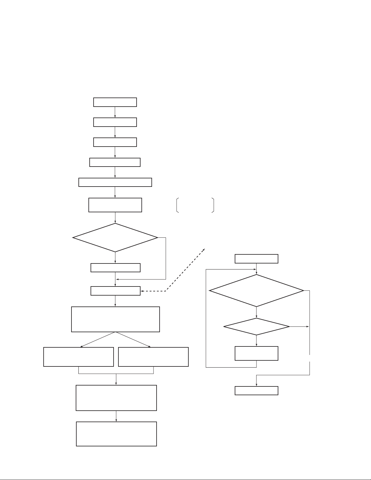
7.1 DIAGNOSIS
7.1.1 SEQUNCE AFTER THE POWER ON
XC-IS21T
Note 1 : IC No. or P∗∗ without name indicate the pin No.
of microcomputer.
Standby states
POWER ON
Power is ON.
Transmit the bus data.
Initialize the LCD microcomputer.
DECK control IC starts
the data transfer.
Does CD door open ?
Is P9 and P10 at "H" level ?
Close the CD door.
Initialize the DECK.
Yes
P35 SYSPOWER : "H"
System bus communication (∗1)
Transfer the system POWER ON.
P4 LCD POWER ON : "H"
P53 LCDRST : "L" RESET
Starts the LCD communication (∗2)
Microcomputer
No
P11 : "H"
P28 VOLDATA
P34 VOLCLK
P75 EXPCE
DECK Initialize Sequence
Note ;
∗1 : System bus communication
∗2 : Starts the LCD communication
∗3 : Transfer the Function, Volume, BASS
and TREBLE data to the volume IC.
∗4 : Initial setting of CD decoder IC
∗5 : Initialize the TUNER PLL IC
Transfer
MOTOR ON
Does the DECK Head down ?
(Is the MODE SW OFF ?)
P29 SYSCLK
P46 SYSDATA
P47 SYSREQ
P48 LCDCLK
P49 LCDCE
P50 LCDDATA
P27 VOLCE
P28 VOLDATA
P34 VOLCLK
P17 CDCLK
P18 CDLAT
P19 CDDATA
P65 TXCE
P66 TXODAT
P67 TXCLK
P68 TXIDAT
Check P79 MODE SW
input is "L".
Yes
Perform the following process after
one second after the POWER ON.
Transfer the Function, Volume, BASS
and TREBLE data to the volume IC. (∗3)
Function : CD (∗4)
Initial setting of CD decoder IC.
P22 CDCONT : "L"
Perform the following process after
3.9 seconds after the POWER ON.
Release the system MUTE.
P71 SYSMUTE : "H"
Perform the following process after
4.0 seconds after the POWER ON.
Release the speaker relay.
P70 SPCONT : "H"
Function : TUNER (∗5)
Initialize the TUNER PLL IC.
P64 TXPOW : "H"
The condition that MUTE
is not released.
• VOLUME : 0
• DECK Function : excepting PLAY
No
Is three times ?
No
500 msec.
solenoid is ON ?
MOTOR OFF
Yes
IC2601(BU4094) P12 is "H"
IC2601(BU4094) P11 is "L"
Retry it to two times.
57
Page 58
XC-IS21T
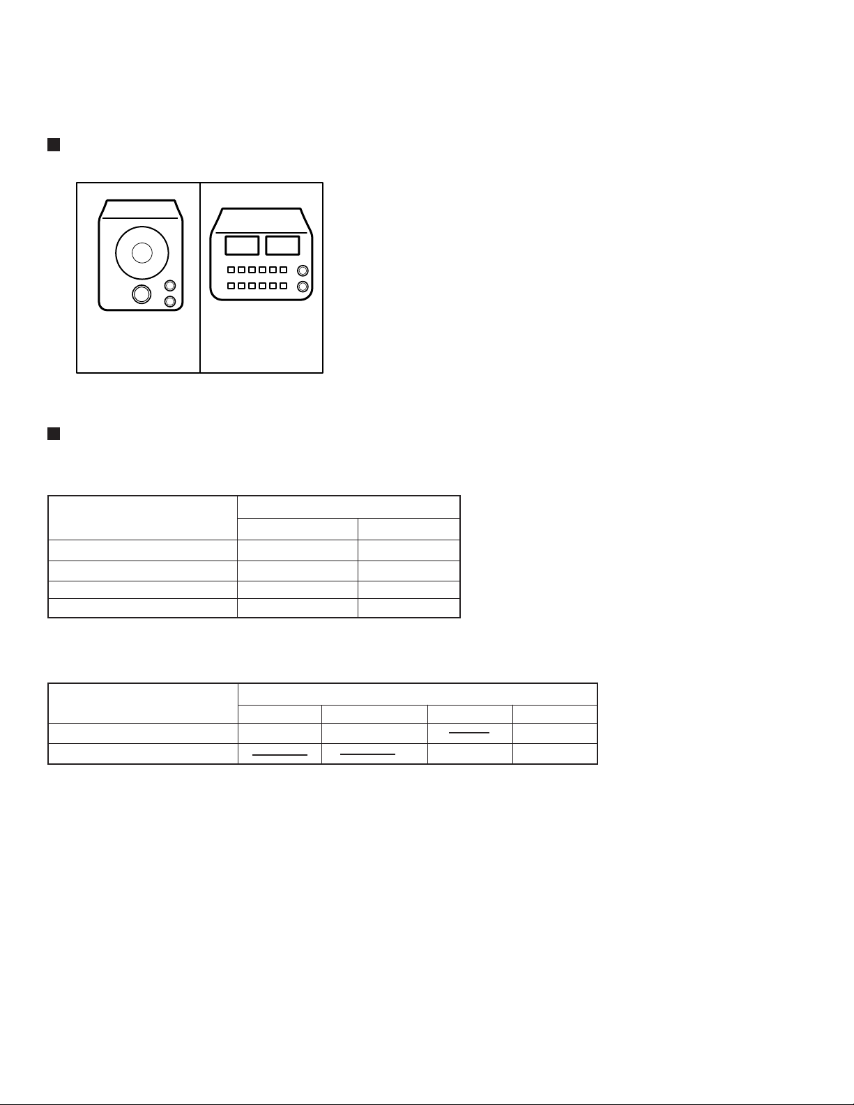
7.1.2 SINGLE OPERATION METHOD
Jigs and Measuring instruments
A
V
Low-frequency
oscillator
DC power-
supplay
Single operation method and frequnency oscilator inputlevel.
1. Connect part A of the AF ASSY [W420(+8V),W421 (+15V), W422 (+5.6V), W423(GND) and DC power-supplay.
(Refer to Fig. 7-1.)
DC power-supplay
Connect point A Voltage (V) Remarks
AF ASSY, W420 (+8v) +8V
AF ASSY, W421 (+15v) +15V
AF ASSY, W422 (+5.6v) +5.6V
AF ASSY, W423 (GND) GND
2. Connect part B of the U-COM ASSY [ CN105 pin8 (AC), AF ASSY[W423 (GND)] and frequency oscillator.
(Refer to Fig. 7-1 and 7-2.)
Low-frequency oscillator
Connect point B frequency level Gnd Remarks
U-COM ASSY, CN105 pin8 (AC) 50 or 60 Hz Approx.2.0 Vrms Note.
AF ASSY, W423 (GND) osc GND
Note: Set up the low-frequncy oscillator level with in the limits of product moves.
58
Page 59
AF ASSY
E
XC-IS21T
U-COM ASSY
C
A
W420......+8V
W421......+15V
W422......+5.6V
W423......GND
Fig. 7-1
SIDE A
Frequency: 50 or 60Hz
Level: Approx. 2Vrms
GND
CN105 pin8 (AC)
OSC
B
Fig. 7-2
SIDE A
59
Page 60

XC-IS21T
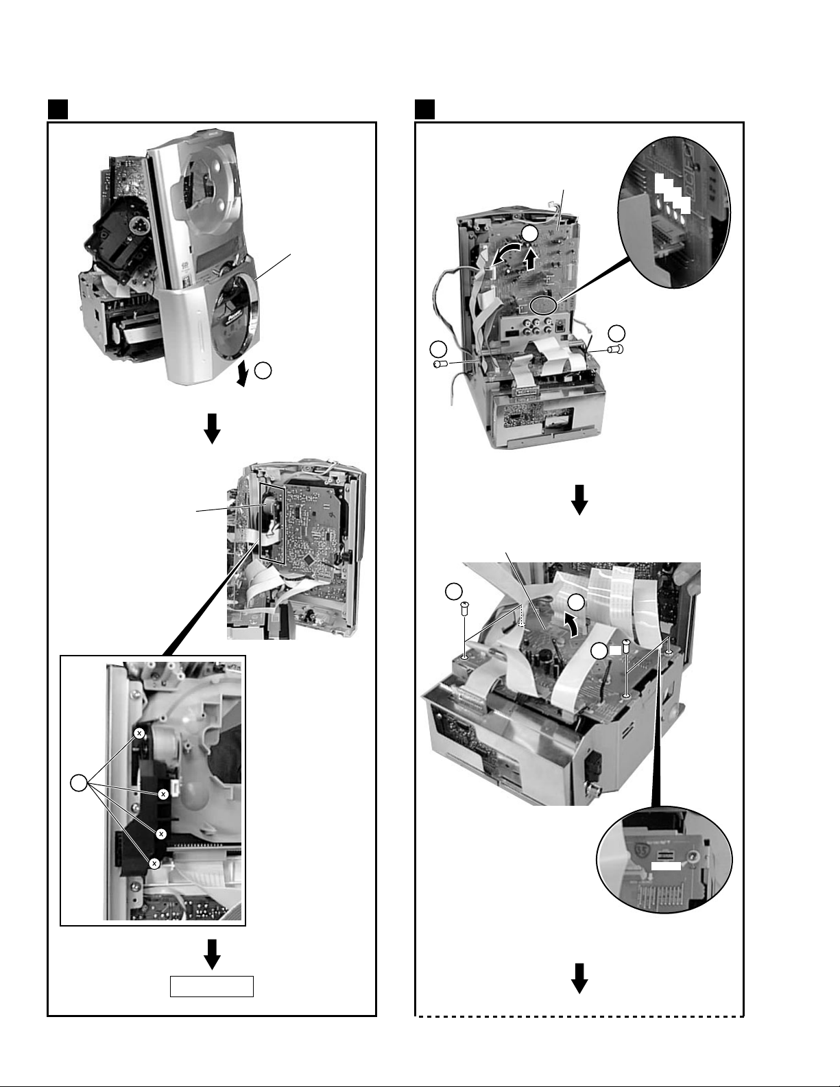
7.1.3 DISASSEMBLY
Front Panel Assy
1
1
×2
1
1
×2
Note : Flexible cables are not removed in the case of the adjustment, but remove
the Flexible cables to apply in the case of the exchange or repair.
• Bottom View
Front Side
Hook off
7
Rear Cover
66
1
×2
1
1
8
8
Clamper
1
×2
2
×2
Earth Lead Wire
4
AFAssy
5
CN7
3
PC Support
Cutting Pliers
Earth Lead Wire
4
Flexible Cable
Caution : Style the Flexible Cables as before so that cables may
not be put in the Rear Cover when assembling it.
×2
Front Panel Assy
9
60
Page 61

CD Mechanism Assy
2
1
XC-IS21T
CD Assy
×2
CD Mechanism Assy
5
5
2
5
Shield Plate
CD Mechanism Assy
CD Assy
3
3
3
4
Caution : When the CD Assy is pulled out, it is careful of the
breaking down of the Flexible Cable.
Exchange
6
61
Page 62
XC-IS21T
CD Door Drive Block Deck Mechanism Unit
3 4
CD Door Drive Block
CD Door
1
Remove the CD Door
1
U-COM Assy
2
AF Assy
GND
Independent power
supply point
1
+5.6V
+15V
+8V
3
×2
4
×2
3
2
×4
TEST 2
Test Point
Exchange
62
Page 63
XC-IS21T
5
DECK Assy
6
DECK Assy Adjustment Point
Slide
Note
CD Door OPEN/CLOSE
1
When a connector CN7 of AF Assy is removed for the touch
5
VR2301
PB L
VR2302
PB R
sensor system, sensor does not work and CD Door can't
open and close. CD Door can open when the land of CN7
at the foil side is short-circuited with the finger.
OPEN/CLOSE
CD Door
CN7
AF Assy
VR2701
SPEED
DECK
Mechanism Unit
7
7
VR2801
BIAS L
VR2802
BIAS R
8
VR2401
REC R
VR2402
REC L
7
DECK Assy
7
FM/AM TUNER Module for European model
2
Shield Case is being soldered in the European model.
Remove solder in the case such as exchange.
Remove
solder
(top side)
FM/AM TUNER Module
Remove
solder
(bottom side)
Exchange, Repair
63
Page 64

XC-IS21T
7.1.4 PCB LOCATION
CD ASSY
F
N
CD CLOSE SW
ASSY
G
CD MOTOR
ASSY
M
CD OPEN SW
ASSY
LCD ASSY
D
LIGHT-L ASSY
L
FRONT PANEL ASSY
K
E
AF ASSY
H
R-TERMINAL ASSY
C
U-COM ASSY
64
I
F-TERMINAL ASSY
J
DECK ASSY
B
TX CONECT ASSY
A
TUNER MODULE
REAR
Page 65

XC-IS21T
7.2 PARTS
7.2.1 IC
• The information shown in the list is basic information and may not correspond exactly to that shown in the schematic diagrams.
CXA1821M (CD ASSY : IC1101)
• RF AMP. IC
Block Diagram
•
CC
V
20 19 18 17 16 15 14 13 12 11
LD ON
LC / PD
RFE
RFO
FE
FE BIAS
TE
VC
EO
174k
AMP
30k
24k
164k
87k
25p
30k
FOCUS
ERROR AMP
VC
VC
26k
13k
260k
V
EE
VC
TRACKING
ERROR AMP
CC
V
820k
VC
VC
820k
123k
123k
23.8k
23.8k
12p
VC VC
147
BUFFER
30k30k
15k
EE
V
12p
260k
V
1k
CC
V
56k
CC
10k
56k
10k
VREF
1.25V
55k
10k
AMP
APC LD
24k
5.6k
RF EQ AMP
10k28k
EE
V
EE
V
30k
24k
22k
VC
VC
30k
25p
RF SUMMING
24k
1 2 3 4 5 6 7 8 9 10
LD
Pin Function
•
No. Pin Name I/O Function No. Pin Name I/O Function
1 LD O APC amplifier output 11 EO
2 PD I APC amplifier input 12 VC O DC voltage output of (VCC+VEE)/2
3A
4 B 14 FE BIAS I Pin for focus bias adjustment
5 C 15 FE O Focus error amplifier output
6 D 16 RFO O RF amplifier output
7 VEE
8F
9 E 19 LD ON I
10 EI
I RF amplifier and FE amplifier input
−
I Tracking error amplifier input.
−
PD
Ground pin 17 RFE
Gain adjust the signal which was input from
pin 9.
A
B
C
D
13 TE O
18 LC/PD I Bias pin VCC : LC , OPEN : PDIC
20 VCC
EE
V
F
Gain adjust the signal which was input from
−
pin 9.
Tracking error amplifier output
F-E signal is output.
−
Pin for RF amplifier equalization
ON/OFF switching pin of APC amplifier
VCC : ON, VEE : OFF
−
Power supply pin
E
EI
65
Page 66

XC-IS21T
CXD2587Q (CD ASSY : IC1201)
• SERVO IC
Block Diagram
•
RFAC
ASYI
ASYO
BIAS
XPCK
FILO
FILI
PCO
CLTV
MDP
LOCK
SENS
DATA
XLAT
CLOK
SPOA
SPOB
XLON
SCOR
SQSC
SQCK
51
49
48
50
17
54
55
56
53
26
25
12
13
14
20
XTSL
37
Clock
Generator
Asymmetry
Corrector
Digital
PLL
Digital
CLV
XUGF
GFS
EMPH
WFCK
C2PO
LRCK
PCMD
BCK
16 18 64 15 19 61 62 63 4
Error
Corrector
EFM
Demodurator
16k
RAM
Sub Code
Processor
D/A
Interface
Digital
OUT
Senal-In
Interface
Over Sampling
Digital Filter
PWM PWM
SYSM
3rd-Order
Noise Shaper
Timing
Logic
36
35
79
80
66
67
3
TES1
TEST
XRST
RMUT
LMUT
XTAI
XTAO
8
5
6
7
CPU
Interface
1
2
Servo
Auto
Sequencer
DAC Block
Signal Processor
Block
70
71
72
77
76
75
60
AOUT1
AIN1
LOUT1
AOUT2
AIN2
LOUT2
DOUT
66
RFDC
CE
TE
SE
FE
VC
IGEN
43
42
41
40
39
38
46
Servo Block
OP-Amp
Analog SW
A/D
Converter
44
ADIO
SERVO
Interface
MIRR
DFCT
FOK
SERVO DSP
FOCUS SERVO
TRACKING
SERVO
SLED SERVO
PWM GENERATOR
FOCUS PWM
GENERATOR
TRACKING PWM
GENERATOR
SLED PWM
GENERATOR
21
27
11
22
23
24
32
33
30
31
28
29
9
SCLK
COUT
SSTP
ATSK
MIRR
DFCT
FOK
FFDR
FRDR
TFDR
TRDR
SFDR
SRDR
Page 67

XC-IS21T
Pin Function
•
¡N-
Pin Name I/O Function No. Pin Name I/O Function
o.
1 SQSO O
2 SQCK I Clock input for SQSO readout 42 CE I Center servo analog input
3 XRST I System reset Reset when "L" 43 RFDC I RF signal input
4 SYSM I Mute input Mute when "H" 44 ADIO O OP amplifier output
5 DATA I Serial data input from CPU 45 AV
6 XLAT I
7 CLOK I Serial data transfer clock input from CPU 47 AV
8 SENS O SENS output to CPU 48 ASYO O EFM full-swing output ("L"=VSS, "H"=VDD)
9 SCLK I Clock input for SENS serial-data readout 49 ASYI I Asymmetry comparate voltage input
10 V
DD
11 ATSK I/O Input and output for unti-shock 51 RFAC I EFM signal input
12 SPOA I Microcomputer extended interface (input A) 52 AV
13 SPOB I Microcomputer extended interface (input B) 53 CLTV I VCO control voltage input for master
14 XLON O Microcomputer extended interface (output) 54 FILO O Filter output for master PLL (Slave=digital PLL)
15 WFCK O WFCK output 55 FILI I Filter input for master PLL
16 XUGF O
17 XPCK O
18 GFS O
19 C2PO O
20 SCOR O
21 COUT I/O Input and output of track-number count signal 61 LRCK O D/A interface LR clock output f=Fs
22 MIRR I/O Mirror signal input and output 62 PCMD O
23 DFCT I/O Defect signal input and output 63 BCK O D/A interface Bit clock output
24 FOK I/O Focus OK signal input and output 64 EMPH O
25 LOCK I/O
26 MDP O Servo control output of spindle motor 66 XTAI I
27 SSTP I Detection signal input of disc innermost 67 XTAO O Crystal oscillation circuit output
28 SFDR O
29 SRDR O 69 AV
30 TFDR O
31 TRDR O 71 AIN1 I L ch OP amp. input
32 FFDR O
33 FRDR O 73 AV
SS
34 V
35 TEST I
36 TEST I 76 AIN2 I R ch OP amp. input
37 XTSL I
38 VC I Center voltage input 78 AV
39 FE I Focus error signal input 79 RMUT O R ch zero detection flag
40 SE I Sled error signal input 80 LMUT O L ch zero detection flag
Notes)
• PCMD is an MSB first. two's complement output.
• GTOP is used to monitor the frame sync protection status. (High:sync protection window released)
• XUGF is the negative pulse for the frame sync derived from the EFM signal. It is the signal before sync protection.
• XPLCK is the inverse of the EFM PLL clock. The PLL is designed so that the falling edge of XPLCK and the EFM signal transition point coincide.
• GFS goes high when the frame sync and the insertion protection timing match.
• RFCK is derived with the crystal accuracy. This signal has a cycle of 136µs.
• C2PO represents the data error status.
• XRAOF is generated when the 16K RAM exceeds the ±4F jitter margin.
SubQ 80-bit, PCM peak and level data output
CD TEXT data output
Latch input from CPU
Serial data is latched at the falling edge.
− Digital power supply 50 BIAS I Constant current input of the asymmetry circuit
XUGF output MNT1 and RFCK output by
switching the command.
XPLCK output MNT0 output by switching the
command.
GFS output MNT3 and XRAOF output by
switching the command.
C2PO output GTOP output by switching the
command.
Outputs "H" when either subcode sync. S0 or S1 is
detected.
GFS is sampled at 460Hz;when GFS is "H", this pin
outputs "H". If GFS is "L" eight consecutive
samples, this pin outputs "L". Input when LKIN="H".
Sled drive output
Tracking drive output
Focus drive output
− Digital GND 74 AVSS2 − Analog GND
TEST pin : normally GND
Crystal selector input
"L":16.9344MHz , "H":33.8688MHz
41 TE I Tracking error input
SS
0 − Analog GND
46 IGEN I Constant current input for OP amplifier
DD
0 − Analog power supply
SS
3 − Analog GND
56 PCO O Charge pump output for master PLL
57 AV
DD
3 − Analog power supply
SS
58 V
59 V
DD
60 DOUT O DIGITAL OUT output
DD
65 XV
SS
68 XV
DD
1 − Analog power supply
70 AOUT1 O L ch analog output
72 LOUT1 O L ch LINE output
SS
1 − Analog GND
75 LOUT2 O R ch LINE output
77 AOUT2 O R ch analog output
DD
2 − Analog power supply
− Digital GND
− Digital power supply
D/A interface
Serial data output (two's complement, MSB first)
Outputs "H" when the playback disc has emphasis,
and "L" when there is no emphasis.
− Power supply for master clock
Crystal oscillation circuit input
Input the external master clock via this pin.
− GND for master clock
67
Page 68
XC-IS21T
PDG242 (U-COM ASSY : IC5501)
• System Control IC
Pin Function
•
No. Name I/O Description
1 TCRECF I Mecha RECF SW
2 TCTIN O TAPE Tray load in
3 TCTOUT O TAPE Tray load out
4 LCD POWER O LCD ON/OFF
5 LIGHT O LCD Buck light control
6 CDDSW1 I CD Door detection Input 1
7 CDDSW2 I CD Door detection Input 2
8 STBYLED O Standby LED control
9 CDDSW3 I CD Door detection Input 3
10 CDDSW4 I CD Door detection Input 4
11 CDCOLSE O CD Door close drive output
12 CDOPEN O CD Door open drive output
13 CD LDON I CD laser diode control output
14 CDINSID I CD inside SW input
15 CDSCLK O CD automatick adjustment input clok
16 CDSENS I CD LSI replay (GFS, FOK)
17 CDCLK O CD LSI clock
18 CDLAT O CD LSI latch
19 CDDATA O CD LSI data
20 CDSYSM O CD decoder mute control
21 CDRESET O CD LSI reset
22 CDCONT O CD LSI power control
23 CDMUTE O CD mute control
24 LINE2 MUTE O Line2 mute control
25 LINE1 MUTE O Line1 mute control
26 LINE CONT O Line ATT control
27 VOLCE O E-Volume LSI chip enabled
28 VOLDATA O E-Volume LSI data
29 SCLK O System bus clock
30 RST
31 EXTAL
32 XTAL
33 Vss
34 VOLCLK O E-Volume LSI clock
35 SYSPOW O System power control
36 AVSS
37 AVREF
38 KEY1 O Key input
39 KEY2 O Key input
40 KEY3 O Key input
-
Reset
-
Oscillator pulses
-
( 12MHz)
-
GNDD
-
GNDD
-
+5V
No. Name I/O Description
41 PROTECT O Protect detection input
42 SIMUKE O Model type select input
43 ST/TUNE O TX STREO/TUNED input
44 JOGIN O Multi JOG input
45
--46 SDATA I/O Systembus data
47 SREQ I/O Systembus reqest
48 LCDCLK O LCD micro computer clock
49 LCDCE O LCD micro computer CE
50 LCDDAT O LCD micro computer data
51 CDSQCK O CD SUBQ clock
52 CDSQSO I CD SUBQ data input
53 LCDRST O LCD micro computer reset control
54 TOUCH I Touch sencer input
55 MS I MS Signal input
56
--57 RDSDATA I RDS data input
58 PDSPOW O RDS power control
59 BEEP O beep control
60 ACPULS I AC puls input
61 REMIN I Remote control input
62 CDSCOR I CD SUBQ level input
63 RDSSCLK I RDS clock input
64 TXPOW O TX poer control
65 TXCE O TX LSI chip enabled
66 TXODAT O TX LSI data output
67 TXCLK O TX LSI clock
68 TXIDAT I TX LSI data input
69 TXMUTE O TX mute control
70 SPCONT O Speaker relay control
71 SYSMUTE O System mute control
72 VDD
73 NC
74 TCSENS I Reel pulse
75 EXPCE O EXPIC for CE control
76 TCOPEN O Tray open SW
77 TCCLOSE O Tray close SW
78 TCHALF I Mechanism HALF SW
79 TCMODE I Mechanism mode SW
80 TCRECR I Mechanism RECR SW
-
--
+5.0V
68
Page 69

XC-IS21T
69
Page 70

XC-IS21T
8. PANEL FACILITIES AND SPECIFICATIONS
8.1 PANEL FACILITIES
Front Panel
70
22
Page 71
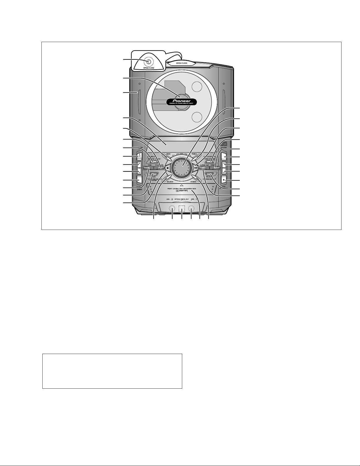
[CD T uner Deck]
#%
&*(·
1
2
3
4
@
XC-IS21T
*
‚
_
6
7
8
9
0
%
=
~
22
!
1 CD cover OPEN/CLOSE touch sensor
2 CD spindle
3 CD slide cover
4 Display window
@ BASS button
6 TUNER button
7 1 • 4 • TUNING – button
8 ST ANDBY/ON button and standby indicator
This is the power switch.
ON : When set to the ON position, power is supplied and the
ST ANDBY : When set to the STANDBY position, the main power flow
Energy-Saving Design
This product has been designed to reduce energy consumption
when the unit is in the power off (standby) mode.
¶ Consult the Specifications for the power consumption in
9 DISPLAY button
0 TIMER REC/WAKE UP/CLOCK ADJ button
% DOLBY* NR ON/OFF (DEMO) button
*¶ Dolby noise reduction manufactured under license from Dolby
Laboratories Licensing Corporation.
¶ “DOLBY” and the double-D symbol are trademarks of Dolby
Laboratories Licensing Corporation.
unit becomes operational.
is cut and the unit is no longer fully operational. A minute
flow of power feeds the unit to maintain operation readiness.
standby mode.
_
+
¡
™
¡
™
∞
¢
= CD button
~ ASES button
! Stop (7) button
& BALANCE button
# LINE 2 IN jack
* OPT (Optical) OUT jack
% LINE 2 OUT jack
( Cassette tray
· ST. (Stereo) WIDE button
* VOLUME/JOG dial
‚ TREBLE button
_ Play/direction (2 3) button
_ TUNING + • ¢ • ¡ button
+ T APE button
¡ ST ATION MEMOR Y button
™ FREQ (Frequency)/ST ATION button
¡ REVERSE MODE button
™ T APE OPEN/CLOSE (0) button
∞ REC/STOP button
¢ LINE 1, 2 button
71
Page 72

XC-IS21T
Display
[CD T uner Deck]
90*
-@ _+¡ $#86 7!
Display window
6 Lights when Dolby NR on optional cassette deck is ON.
7 Lights when using A.S.E.S. (Auto Synchro Editing System).
8 Lights when optional cassette deck is set to recording mode.
9 Lights during program mode.
0 Lights during random playback.
- Lights during repeat playback.
= Lights when setting wake-up timer.
~ Lights during sleep timer operation.
! Lights when setting timer recording.
@ Lights during stereo wide sound mode.
# Lights to indicate tape direction of optional cassette deck.
$ Lights to indicate reverse mode of optional cassette deck.
% Lights during FM stereo reception.
^ Lights when FM monaural reception is ON.
& Lights when setting Beat Cut function.
* Lights during radio broadcast reception.
( Indicates frequency and major operation status.
) Lights when Dolby NR is ON.
_ Lights when cassette deck is set to recording mode.
+ Lights to indicate tape direction of cassette deck.
¡ Lights to indicate reverse mode of cassette deck.
)
=^%&~(
72
Page 73

XC-IS21T
Remote Control Unit
[CD T uner Deck]
1
2
3
4
6
7
8
9
0
=
5
~
!
%
^
&
*
)
0 CD/MD/T APE/TUNER operation buttons
[CD/MD operation]
3/8 : Play/pause button
7 : Stop button
1, ¡ : Manual search buttons
4, ¢ : Track search buttons
[T APE operation]
2 3 : Play button
7 : Stop button
1, ¡ : Fast forward, fast reverse buttons
4, ¢ : Music search buttons
[TUNER operation]
1, ¡ : Frequency down, up buttons
–, + : Memory station no. decrement, increment
buttons
- DISP (display) button
= MONO button
~ T APE button
! T APE open/close (0) button
% LINE 1, 2 button
^ CLR (clear) button
& REPEA T button
* RANDOM button
) VOL (volume) +, – button
Remote control buttons with the same name or mark as buttons on the front panel of the CD Tuner Deck control the same
operations as the corresponding front panel buttons.
1 ST ANDBY/ON button
2 SLEEP button
3 CD button
4 CD cover open/close (0) button
5 TUNER button
6 Digit (1 – 9, 10/0, >10) buttons
7 ST. (stereo) WIDE button
8 PROGRAM button
9 SOUND MODE button
73
Page 74
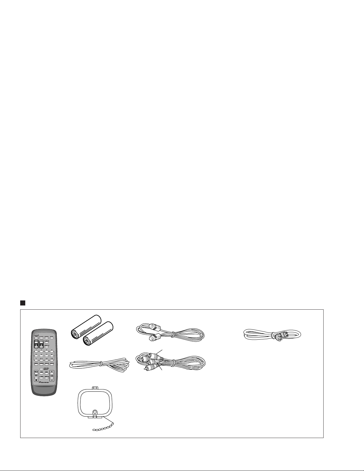
XC-IS21T
8.2 SPECIFICATIONS
7 Amplifier Section
Continuous average power output of 55 watts* per
channel, min., at 6 ohms, from 60 Hz to 15,000 Hz
with no more than 1.0 %** total harmonic distortion.
* Measured pursuant to the Federal Trade Commission’s Trade
Regulation rule on Power Output Claims for Amplifiers.
** Measured by Audio Spectrum Analyzer.
7 FM Tuner Section
Frequency Range ................................................. 87.5 - 108MHz
Antenna............................................................75 Ω, unbalanced
7 AM Tuner Section
Frequency Range ................... 531 kHz - 1,602 kHz (9 kHz step);
530 kHz - 1,700 kHz (10 kHz step)
Antenna..................................................................Loop antenna
7 Compact Disc Player Section
Type .......................................Compact disc digital audio system
Usable discs ......................................................... Compact discs
Wow and Flutter ........................................ Limit of measurement
(0.001%) or less (EIAJ)
7 Cassette Deck Section
System ................................................ 4-track, 2-channel stereo
Heads.............................................Recording/playback head x 1
Erasing head x 1
Motor ............................................................ DC Servo motor x 1
Tape type.......................... TYPE I (Normal), TYPE II (High/CrO2)
7 Micellaneous (Stereo power amplifier : M-IS21)
Power Requirements .......................................... AC120 V, 60 Hz
Power Consumption ............................................. 120 W, 160 VA
Power Consumption in standby mode ................................... 1 W
Dimensions:
CD Tuner Deck
............................................. 205 (W) x 300 (H) x 237 (D) mm
8-1/16 (W) x 11-13/16 (H) x 9-5/16 (D) in.
Power Amplifier .................... 150 (W) x 300 (H) x 233 (D) mm
5-7/8 (W) x 11-13/16 (H) x 9-3/16 (D) in.
Weight:
CD Tuner Deck............................................. 2.9 kg (6 lb 6 oz)
Power Amplifier .......................................... 4.0 kg (8 lb 13 oz)
7 Accessories
Operating Instructions................................................................ 2
Warranty Card ........................................................................... 1
FM antenna .............................................................................. 1
AM loop antenna ....................................................................... 1
Remote control unit .................................................................. 1
Dry cell batteries (AA/R6) .......................................................... 2
Power cord ................................................................................ 1
RCA pin-plug stereo cable ......................................................... 1
System cable............................................................................. 1
7 Accessories
Speaker cords ........................................................................... 2
NOTE:
Specifications and design subject to possible modification without notice, due
to improvements.
Accessories
12
3
4
74
5
6
(Red)
(White)
(L= 1.5m)
7
1 Remote control unit x 1 : AXD7224
(CU-XR056)
2 AA/R6P dry cell batteries x 2 : VEM-013
3 FM antenna x 1 : ADH7004
4 AM Loop antenna x 1 : ATB7007
5 System cable x 1 : ADE7039
6 RCA pin-plug stereo cable x 1 : VDE1052
(L= 1.5m)
7 Power cord x 1 : XDG3007
 Loading...