Pioneer VSX-920-K Service manual

PIONEER CORPORATION 1-1, Shin-ogura, Saiwai-ku, Kawasaki-shi, Kanagawa 212-0031, Japan
PIONEER ELECTRONICS (USA) INC. P.O. Box 1760, Long Beach, CA 90801-1760, U.S.A.
PIONEER EUROPE NV Haven 1087, Keetberglaan 1, 9120 Melsele, Belgium
PIONEER ELECTRONICS ASIACENTRE PTE. LTD. 253 Alexandra Road, #04-01, Singapore 159936
PIONEER CORPORATION
2010
VSX-920-K
AUDIO/VIDEO MULTI-CHANNEL RECEIVER
VSX-920-K
THIS MANUAL IS APPLICABLE TO THE FOLLOWING MODEL(S) AND TYPE(S).
Model Type Power Requirement Remarks
VSX-920-K UXCNCB AC 120 V
This service manual should be used together with the following manual(s).
Model No. Order No. Remarks
ORDER NO.
RRV4048
VSX-820-K/CUXCNSM RRV4043
For SPECIFICATIONS and PANEL FACILITIES, refer to the operating instructions.
K-ZZZ MAR.
2010 Printed in Japan

1
2 3 4
CONTENTS
1. CONTRAST OF MISCELLANEOUS PARTS.........................................................................................................................3
2. BASIC ITEMS FOR SERVICE...............................................................................................................................................5
A
B
C
2.1 JIGS LIST .......................................................................................................................................................................5
3. BLOCK DIAGRAM.................................................................................................................................................................6
3.1 OVERALL WIRING DIAGRAM .......................................................................................................................................6
3.2 OVERALL BLOCK DIAGRAM.........................................................................................................................................8
4. DIAGNOSIS.........................................................................................................................................................................10
4.1 DIAGNOSIS FLOWCHART ..........................................................................................................................................10
5. DISASSEMBLY ...................................................................................................................................................................21
5.1 DISASSEMBLY .............................................................................................................................................................21
6. EACH SETTING AND ADJUSTMENT ................................................................................................................................24
6.1 IDLE CURRENT ADJUSTMENT ..................................................................................................................................24
7. SCHEMATIC DIAGRAM ......................................................................................................................................................26
7.1 INPUT ASSY.................................................................................................................................................................26
7.2 AMP ASSY....................................................................................................................................................................28
7.3 SPEAKER, HEADPHONE and MIC ASSYS.................................................................................................................30
7.4 PT, HP_GUIDE, CNT1, CNT2, GUIDE_L and GUIDE_R ASSYS ................................................................................31
7.5 VIDEO ASSY ................................................................................................................................................................32
7.6 F-VIDEO, FRONT and FUNCTION ASSYS..................................................................................................................34
7.7 MAIN and REG ASSYS ................................................................................................................................................36
7.8 HDMI ASSY (1/2)..........................................................................................................................................................38
7.9 HDMI ASSY (2/2)..........................................................................................................................................................40
7.10 DSP ASSY (1/2)..........................................................................................................................................................42
7.11 DSP ASSY (2/2)..........................................................................................................................................................44
7.12 USB ASSY ..................................................................................................................................................................46
8. PCB CONNECTION DIAGRAM ..........................................................................................................................................48
8.1 INPUT ASSY.................................................................................................................................................................48
8.2 AMP ASSY....................................................................................................................................................................50
8.3 SPEAKER, HEADPHONE and MIC ASSYS.................................................................................................................54
8.4 PT, HP_GUIDE, CNT1, CNT2, GUIDE_L and GUIDE_R ASSYS ................................................................................56
8.5 VIDEO ASSY ................................................................................................................................................................58
8.6 MAIN and REG ASSYS ................................................................................................................................................60
8.7 HDMI ASSY ..................................................................................................................................................................64
8.8 DSP ASSY ....................................................................................................................................................................66
8.9 USB ASSY ....................................................................................................................................................................68
9. PCB PARTS LIST................................................................................................................................................................70
D
E
F
2
1
2 3 4
VSX-920-K
5
Parts marked by "NSP" are generally unavailable because they are not in our Master Spare Parts List.
The mark found on some component parts indicates the importance of the safety factor of the part.
Therefore, when replacing, be sure to use parts of identical designation.
Screws adjacent to mark on product are used for disassembly.
For the applying amount of lubricants or glue, follow the instructions in this manual.
(In the case of no amount instructions, apply as you think it appropriate.)
Nos. indicate the pages and Nos. in the service manual for the base model.
NOTES:
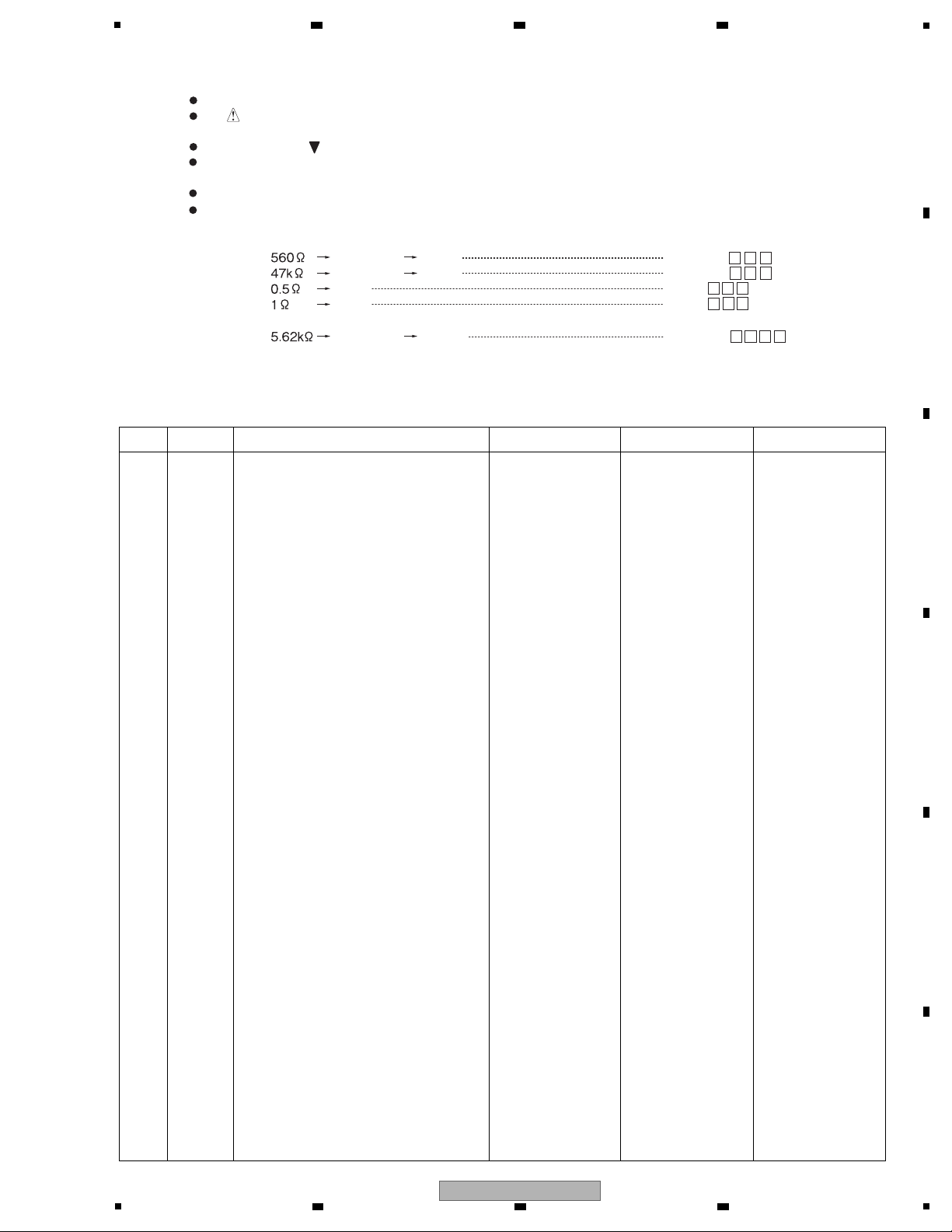
When ordering resistors, first convert resistance values into code form as shown in the following examples.
Ex.1 When there are 2 effective digits (any digit apart from 0), such as 560 ohm and 47k ohm (tolerance is shown by J=5%,
and K=10%).
Ex.2 When there are 3 effective digits (such as in high precision metal film resistors).
5
6 1
4 7 3
R 5 0
1
R 0
RD1/4PU J
RD1/4PU J
RN2H K
RS1P K
56 x 10
1
47 x 103
R50
1R0
561
473
RN1/4PC F562 x 10
1
5621 5 26 1
6 7 8
1. CONTRAST OF MISCELLANEOUS PARTS
CONTRAST TABLE
VSX-820-K/CUXCNSM and VSX-920-K/UXCNCB are constructed the same except for the following:
Mark No. Symbol and Description VSX-820-K/CUXCNSM VSX-920-K/UXCNCB Remarks
PCB ASSEMBLIES
NSP 1..MAIN ASSY 7025HK0916010-IL 7025HK0917060-IL
P68-16 2..MAIN ASSY 7028069111010-IL 7028069321010-IL
P68-6 2..PT ASSY 7028069112010-IL 7028069325010-IL
P68-9 2..CNT2 ASSY 7028069113010-IL 7028069322010-IL
P68-4 2..HEADPHONE ASSY 7028069114010-IL 7028069324010-IL
P68-7 2..HP_GUIDE ASSY 7028069115010-IL 7028069323010-IL
P68-5 2..MIC ASSY 7028069116010-IL 7028069327010-IL
P68-10 2..GUIDE_L ASSY 7028069117010-IL 7028069328010-IL
P68-11 2..GUIDE_R ASSY 7028069118010-IL 7028069329010-IL
P68-8 2..CNT1 ASSY 7028069119010-IL 7028069326010-IL
A
B
C
NSP 1..VIDEO ASSY 7025HK0916013-IL Not used
P68-12 2..VIDEO ASSY 7028069141010-IL Not used
NSP 1..VIDEO ASSY Not used 7025HK0917062-IL
P68-12 2..VIDEO ASSY Not used 7028069301010-IL
P68-3 2..SPEAKER ASSY Not used 7028069302010-IL
NSP 1..FRONT ASSY 7025HK0916011-IL 7025HK0917067-IL
P68-13 2..F-VIDEO ASSY 7028069123010-IL 7028069124010-IL
NSP 1..INPUT ASSY 7025HK0916012-IL 7025HK0917061-IL
P68-1 2..INPUT ASSY 7028069131010-IL 7028069291010-IL
NSP 1..SPEAKER ASSY 7025HK0916014-IL Not used
P68-3 2..SPEAKER ASSY 7028069151010-IL Not used
NSP 1..DSP ASSY 7025HK0916015-IL 7025HK0917063-IL
P68-19 2..DSP ASSY 7028069161010-IL 7028069311010-IL
P68-17 2..REG ASSY 7028069162010-IL 7028069312010-IL
NSP 1..HDMI ASSY 7025HK0916018-IL 7025HK0917064-IL
P68-18 2..HDMI ASSY 7028069191010-IL 7028069331010-IL
NSP 1..USB ASSY 7025HK0916016-IL 7025HK0917066-IL
P68-20 2..USB ASSY 7028069171010-IL 7028069173010-IL
5
6 7 8
VSX-920-K
D
E
F
3
1
2 3 4
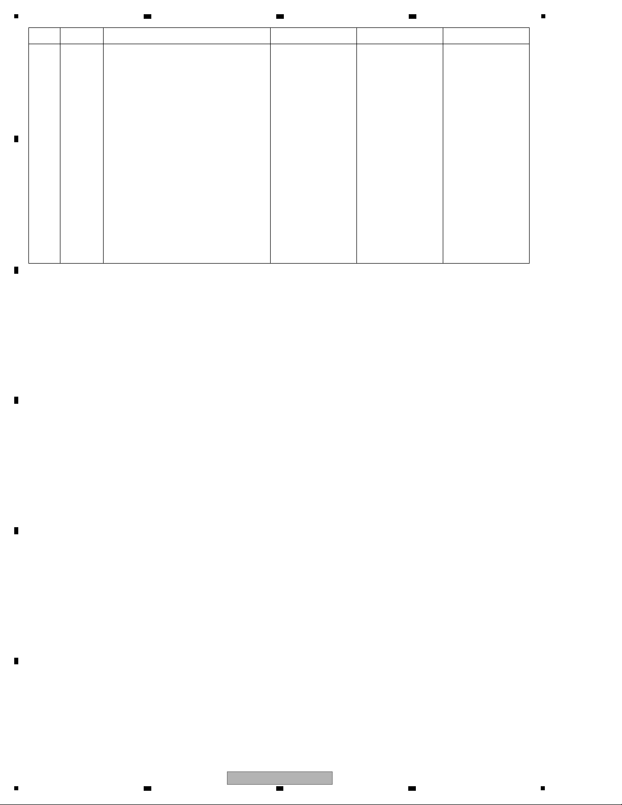
Mark No. Symbol and Description VSX-820-K/CUXCNSM VSX-920-K/UXCNCB Remarks
NSP 1..AMP ASSY 7025HK0916019-IL 7025HK0917065-IL
P68-2 2..AMP ASSY 7028067523010-IL 7028069231020-IL
A
PACKING SECTION
P65-7 Operating Instructions (En/Frca/Es) 5707000003160-IL Not used
Operating Instructions (En/Sp) Not used 5707000003260-IL
P65-10 Box, Gift 6007211700060-IL 60072117000D0-IL
EXTERIOR SECTION
P68-22 Power Trans. 8200960610590-IL 8200960610700-IL
P68-27 Cable, Flat Card 1.25 N712232533810-IL N712232513880-IL
P68-30 Sheet 1210210762000-IL 1210211232000-IL
P68-35 Panel Front 3067214861000-IL 3067214861010-IL
B
P68-38 Chassis Back 3207213456000-IL 3207213456400-IL
Posistor Not used F320121021240-IL No. 69
NSP Label Getter 920U Not used 5507000004550-IL
NSP Label Hot Surface Not used 5507000003730-IL
C
D
E
F
4
1
2 3 4
VSX-920-K
5
×7
×5
×5
×6
×3
×21
×7
×7
C
F
Q
F
B
F
Jigs List
Jig Name Part No. Remarks
RS-232C upgrade jig GGF1642
Firmware upgrade (RS-232C ↔ Rear panel)
10P to 8P FFC GGF1676
Board to board extension jig cable GGD1674 Diagnosis (DSP Assy ↔ MAIN Assy)
13P extension jig cable GGD1669 Diagnosis (AMP Assy ↔ INPUT Assy)
8P extension jig cable GGD1670 Diagnosis (AMP Assy ↔ MAIN Assy)
7P extension jig cable GGD1671 Diagnosis (AMP Assy ↔ SPEAKER Assy)
2P short connector jig GGD1672 Diagnosis (Posistor ↔ MAIN Assy)
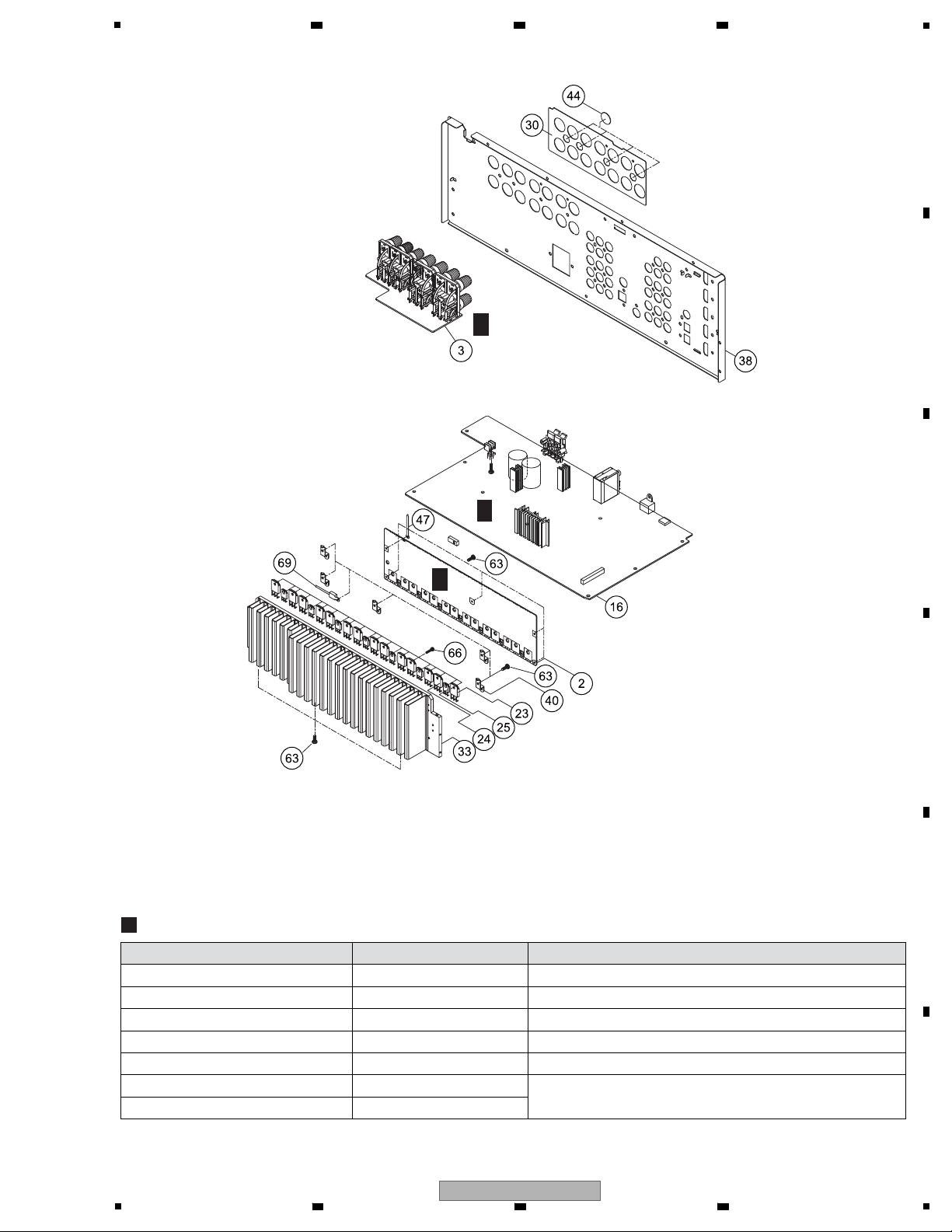
EXPLODED VIEWS
EXTERIOR SECTION
6 7 8
A
B
2. BASIC ITEMS FOR SERVICE
2.1 JIGS LIST
C
D
E
5
VSX-920-K
6 7 8
F
5
1
AMP ASSY
(7028069231020-IL)
SPEAKER ASSY
(7028069302010-IL)
HEADPHONE ASSY
(7028069324010-IL)
REG ASSY
(7028069312010-IL
O
P
FUNCTION ASSY
(7028069122010-IL)
USB ASSY
(702806917301
BT ASSY (702806918101
R
F
U
F
D
F
B
F
C
F
2 3 4
3. BLOCK DIAGRAM
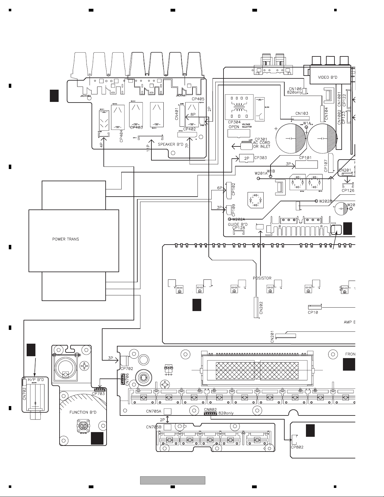
3.1 OVERALL WIRING DIAGRAM
A
B
C
D
E
F
6
1
VSX-920-K
2 3 4
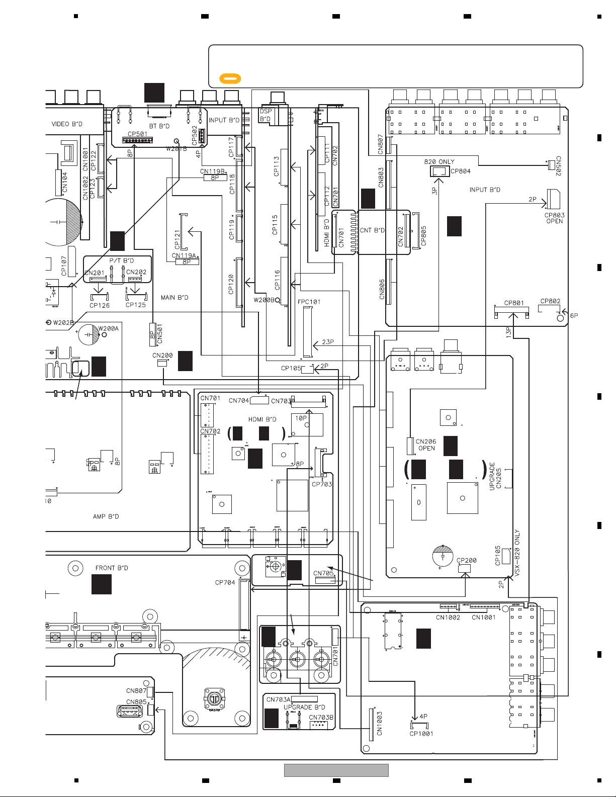
-
When ordering service parts, be sure to refer to "EXPLODED VIEWS and PARTS LIST" or "PCB PARTS LIST".
-
The > mark found on some component parts indicates the importance of the safety factor of the part.
Therefore, when replacing, be sure to use parts of identical designation.
-
: The power supply is shown with the marked box.
MAIN ASSY
(7028069321010-IL)
VIDEO ASSY
(7028069301010-IL)
HDMI ASSY
(7028069331010-IL)
CNT2 ASSY
(7028069322010-IL)
INPUT ASSY
(7028069291010-IL)
CNT1 ASSY
(7028069326010-IL)
PT ASSY
(7028069325010-IL)
F-VIDEO ASSY
(7028069124010-IL)
O
FRONT ASSY
(7028069121010-IL)
V
MIC ASSY
(7028069327010-IL)
DSP ASSY
(7028069311010-IL)
T T
1/2, 2/2
T
F
A
F
I
F
G
F
Q
F
R
F
S
F
E
F
M
F
N
F
J
F
F
S S
1/2, 2/2
CN201CN207CN208
5
6 7 8
A
B
C
D
E
F
5
6 7 8
VSX-920-K
7
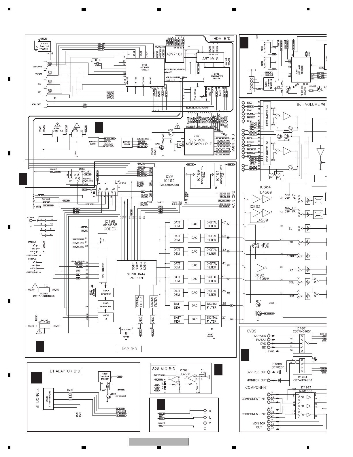
1
B D0-D11
G Q12-Q23
R Q24-Q35
R D-24-D35
B Q0-Q11
RXODCK
RXDE
RXHSYNC
RXVSYNC
G D12-D23
RX_MCK,SDO/DLO,SCK/DCK,WS/DRO
VIDEO ASSY
INPUT ASSY
INPUT ASSY
INPUT ASSY
MAIN ASSY
MAIN ASSY
INPUT
ASSY
VIDEO
ASSY
HDMI ASSY
USB
ASSY
MAIN ASSY
MIC
ASSY
DSP ASSY
V
BT ASSY
F-VIDEO ASSY
U
F
S
F
Q
F
T
F
E
F
M
F
N
F
2 3 4
3.2 OVERALL BLOCK DIAGRAM
A
B
C
D
E
F
8
1
2 3 4
VSX-920-K
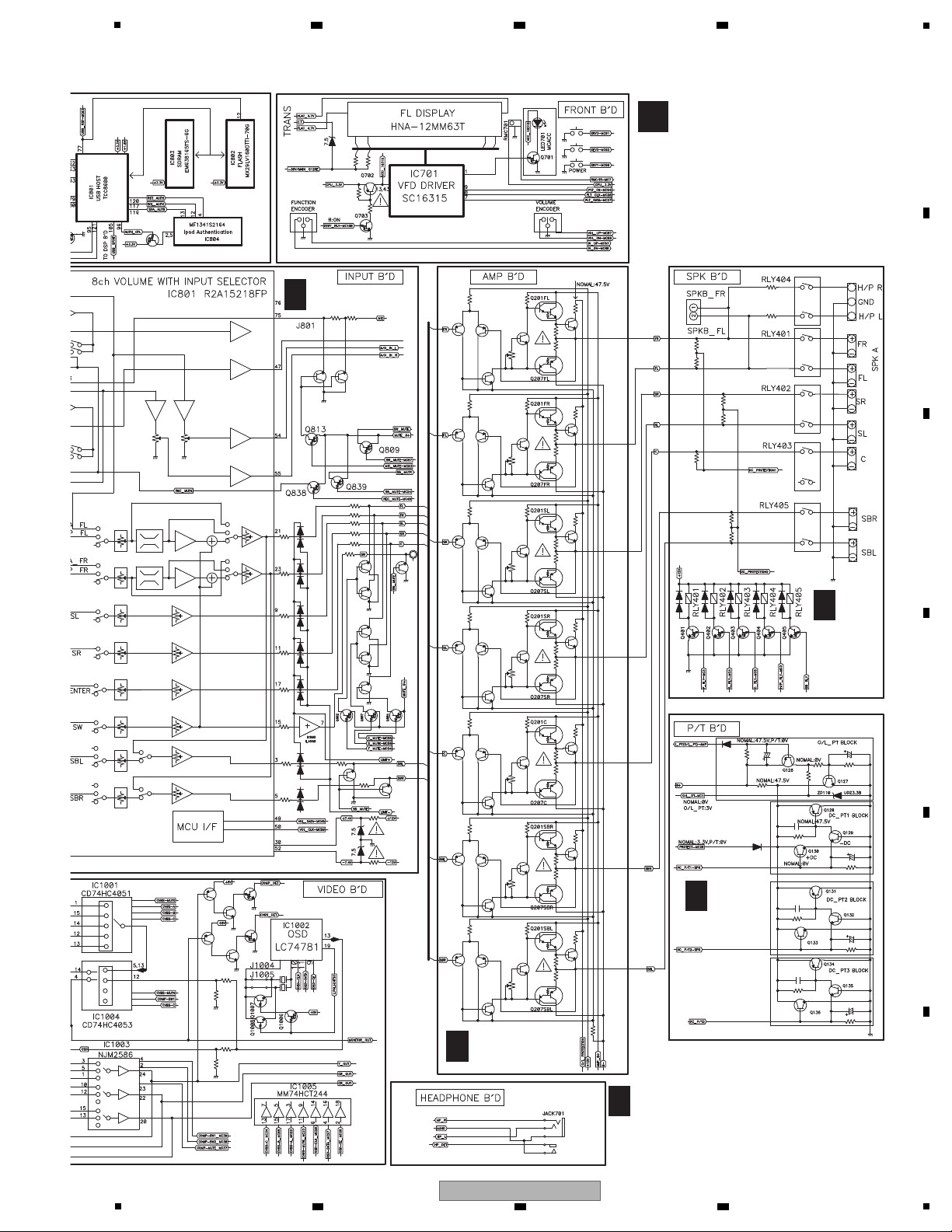
5
HEADPHONE ASSY
SPEAKER
ASSY
PT ASSY
INPUT ASSY
MAIN ASSY
MAIN ASSY
SPEAKER
ASSY
AMP ASSY
O
FRONT ASSY
A
F
B
F
D
F
G
F
C
F
6 7 8
A
B
C
D
E
5
6 7 8
VSX-920-K
F
9
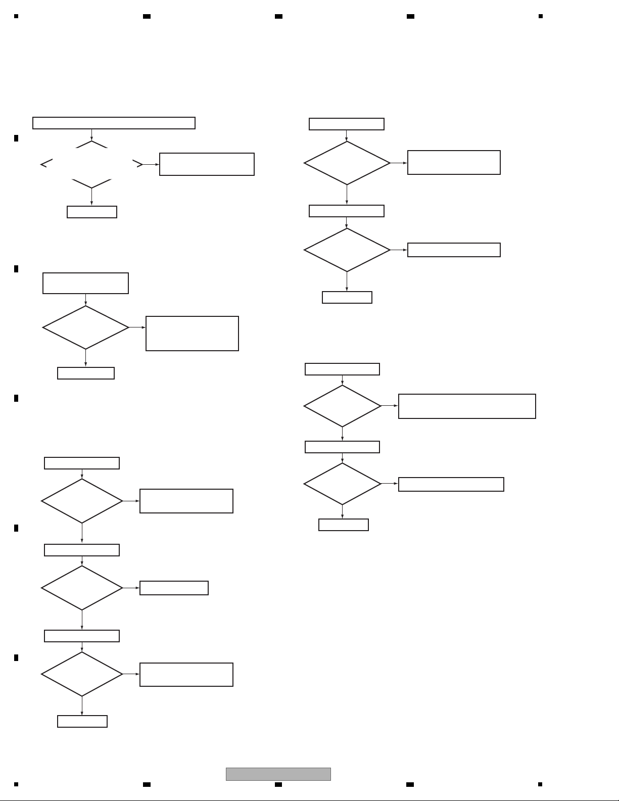
1
Step 3: Regulator IC
REG101 (Pin 3)
Is the
voltage of around
3.3 V input?
Replace REG103.
Check the ZD200 3.0B
and IC106.
To Step 3
To Step 4
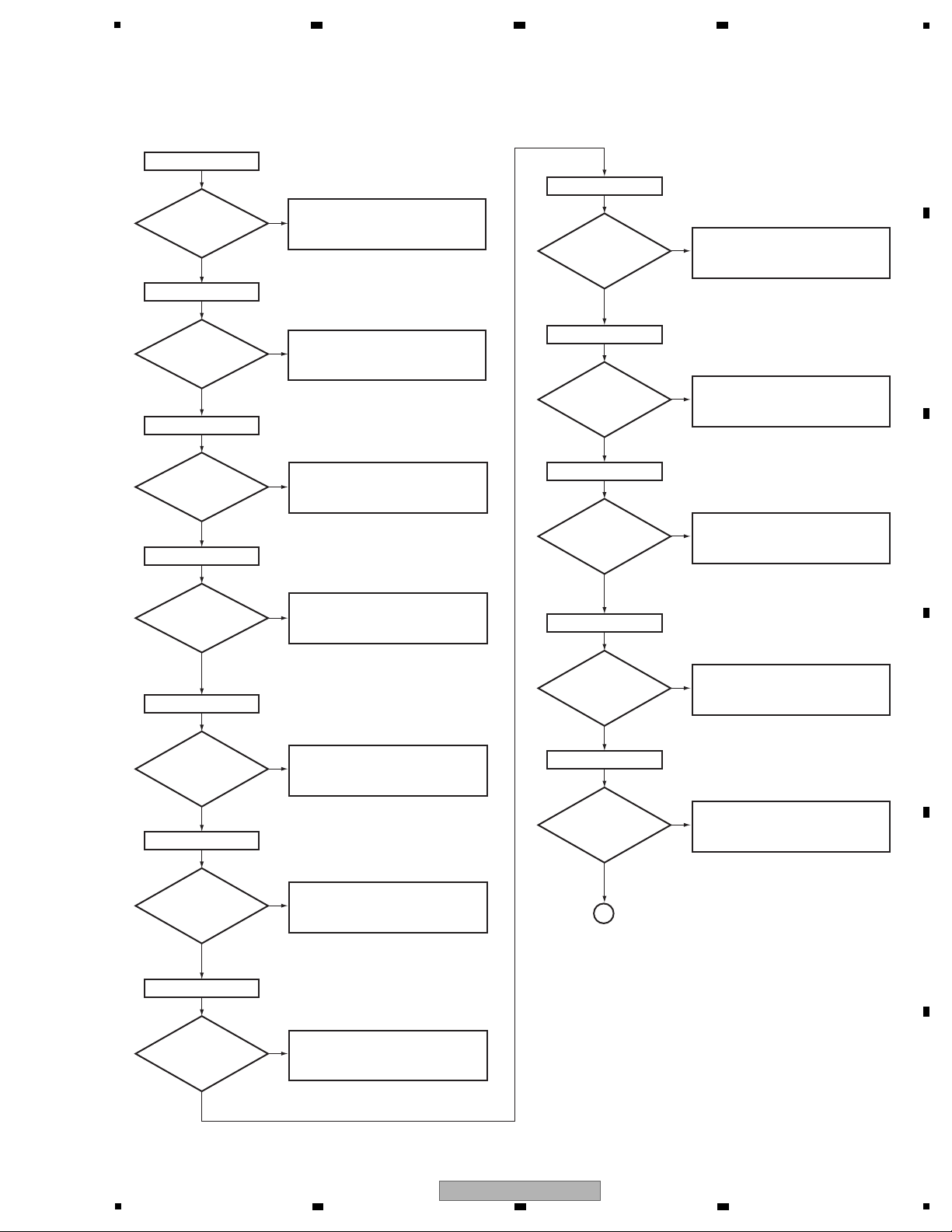
Step 0: Preliminary confirmation
Confirm the following items before checking
Tighten screws securely.
No
Yes
To Step 1
No
[1] DSP TROUBLESHOOTING
Step 2: Regulator IC
Check the REG101,
and MAIN Assy
Check the REG103 and
MAIN Assy.
REG103 (Pin 3)
Is the
voltage of around
5 V input?
No
Yes
(to chassis)
ZD200 cathode
Is the
voltage of 3.0 V
output?
No
*The I/O power of DSP Assy is OK.
*The IC106 power of DSP Assy
*The DSP IC CORE power of DSP Assy
XMCK
REG103 (Pin 2)
Is the
voltage of 3.3 V
output?
No
Yes
Yes
Yes
Is the
voltage of 1.2 V
output?
Replace REG101.
Check the path to XTAL101.
No
Yes
(to chassis)
(to chassis)
REG101 (Pin 2)
(to chassis)
Step 1: BtoB connector, wire
CN201,CN207,CN208,
CP200,CP105
Are the
connectors securely
inserted?
Turn the power off and
insert the connectors
securely.
No
Yes
To Step 2
*CP200 connectors doesn't connection
in case of DSP JIG B'D use.
BtoB connector, wire
Do screws of COAX
Jack securely tighten?
OR connect GND wire of
DSP JIG B'D to chassis.
Step 4: X'tal
To Step 5
Yes
IC109 (Pin 6, 7)
No
Is there
a 24.576 MHz
output?
Check the path to pins 6, 7 of IC109.
Replace XTAL101.
Yes
IC102 (Pin 17)
No
Is there
a 24.576 MHz
input?
4. DIAGNOSIS
4.1 DIAGNOSIS FLOWCHART
A
2 3 4
B
C
D
E
F
10
1
VSX-920-K
2 3 4
5
Replace IC109.
Yes
IC109 (Pin 15)
DIR_BCK (Bit clock)
No
Is there
a bit clock
output?
(0 V ⇔ 3.3 V)
Yes
IC106 (Pin 4)
DAI_MCK (Master clock)
Is there
a master clock
output?
(0 V ⇔ 3.0 V)
Yes
IC106 (Pin 7)
DAI_LRCK (LR clock)
Is there
a LR clock
output?
(0 V ⇔ 3.0 V)
Yes
IC106 (Pin 9)
DAI_BCK (Bit clock)
*IC106 Pin 1
0 V : DIR
3.3 V : HDMI
Is there
a bit clock
output?
(0 V ⇔ 3.0 V)
Replace IC106.
Check the path
between IC106-pin 1
and MAIN Assy.
No
No
No
No
Is the
voltage of
IC106-pin 1
0 V?
Yes
Switch
Step 5: DIR
Check the path to pins 10-13
of IC110 or replace IC110.
Check the path to CP105 connector.
Replace IC109.
Check the path to OUTPUT PIN of
JACK105, JACK106.
IC110 (Pins 3, 5)
OPTICAL (Pin 3: OPT2, Pin 5: OPT1)
Check that the S/PDIF signal is output.
Check that changes by pulling out and inserting the digital input lines.
Can
observe the
digital signal
?
No
(0 V ⇔ 3.3 V)
Yes
IC109 (Pin 67)
COAX
Can
observe the
digital signal
?
No
Yes
Yes
Check that the data and clock signals are output.
Check that it changes in the Playback and Pause modes of
the USB (iPod).
(0 V ⇔ 3.3 V)
(0 V ⇔ 3.3 V)
(0 V ⇔ 3.3 V)
Yes
IC109 (Pin 71)
From USB Assy
Can
observe the
digital signal
?
No
(0 V ⇔ 3.3 V)
Check the path to pins 4, 6 of
IC110 or replace IC110.
IC109 (Pins 61, 63)
OPTICAL (Pin 61: OPT2, Pin 63: OPT1)
Can
observe the
digital signal
?
No
Yes
(0 V ⇔ 3.3 V)
Check the MAIN Assy.
IC109 (Pin 10)
DIR_MCK (Master clock)
No
No
Yes
Is there
a master clock
output?
IC109 (Pin 16)
DIR_LRCK (LR clock)
No
Is there
a LR clock
output?
Replace IC109.
(0 V ⇔ 3.3 V)
Yes
IC109 (Pin 14)
DIR_SDTO (Data)
No
Is there
a data
output?
Is the
voltage of PDN
IC109-pin 31
3.3 V?
Check the USB Assy.
No
To Step 6
6 7 8
A
B
C
D
5
VSX-920-K
6 7 8
E
F
11
1
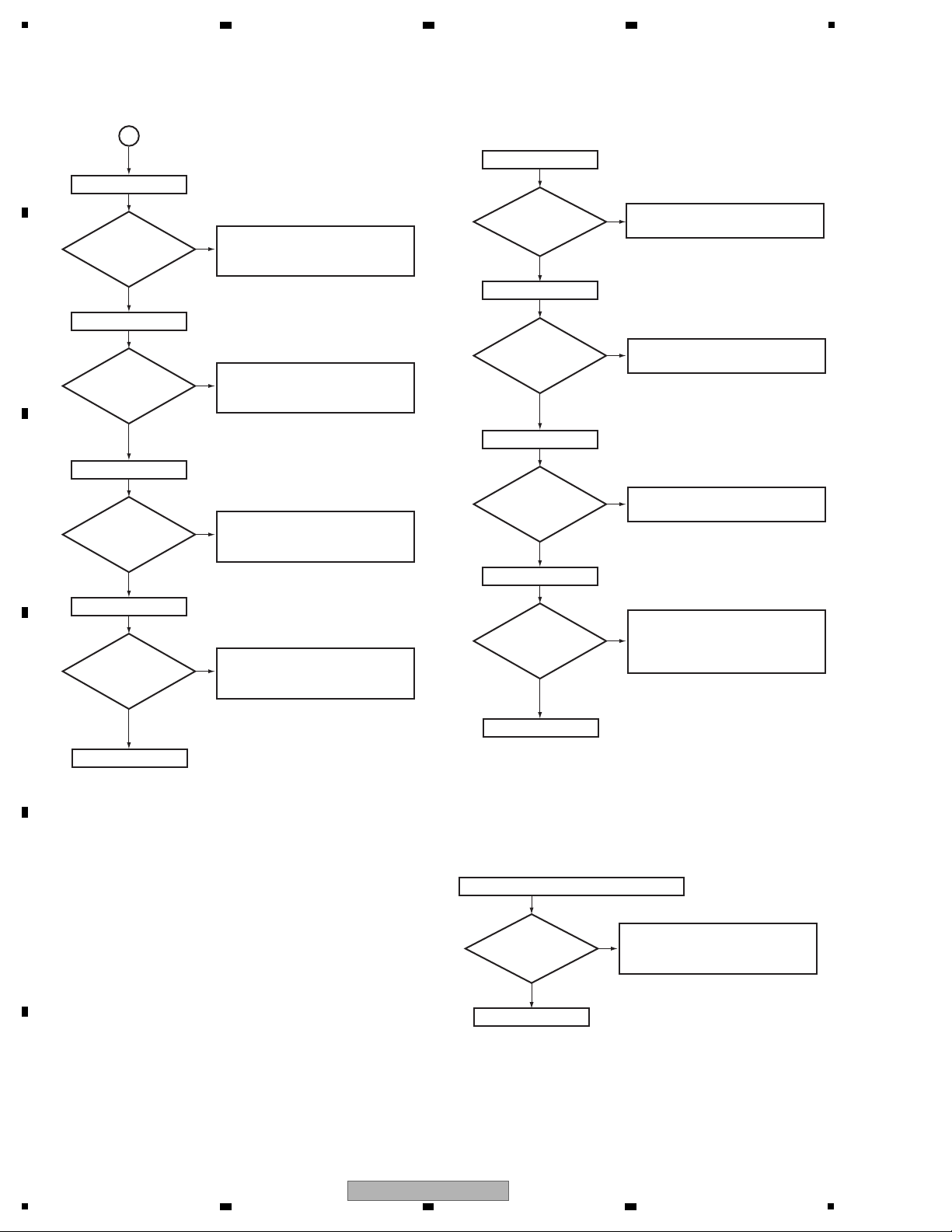
Step 6: DSP output (digital)
Yes
Digital output of each CH when inputting the digital signal with audio.
IC109 (Pin 26)
Center/LFE data
No
Is there
a data input?
Yes
Check the path between IC102
and data & address lines.
SDRAM (IC100), FLASH ROM
(IC101)
IC109 (Pin 25)
Surround back L/R data
No
Is there
a data input?
Yes
IC109 (Pin 27)
Surround L/R data
No
Is there
a data input?
Yes
IC109 (Pin 18)
DSP_BCK (Bit clock)
No
Is there
a bit clock
input?
Yes
IC109 (Pin 19)
DSP_LRCK (LR clock)
No
Is there
a LR clock
input?
Yes
IC109 (Pin 28)
Front L/R data
No
Is there
a data input?
(0 V ⇔ 3.3 V)
(0 V ⇔ 3.3 V)
(0 V ⇔ 3.3 V)
(0 V ⇔ 3.3 V)
(0 V ⇔ 3.3 V)
(0 V ⇔ 3.3 V)
To Step 7
A
2 3 4
B
C
D
E
F
12
1
VSX-920-K
2 3 4
5
Ye s
Replace IC109.
IC109 (Pin 49)
Front R out
No
Is the output
2.5 V fixing?
Replace IC109.
Ye s
Ye s
IC109 (Pin 43)
Surround L out
No
Is the output
2.5 V fixing?
Replace IC109.
IC109 (Pin 41)
Center out
No
Is the output
2.5 V fixing?
Ye s
Replace IC109.
IC109 (Pin 39)
End
LFE out
No
Is the output
2.5 V fixing?
Ye s
Ye s
Replace IC109.
IC109 (Pin 47)
Front L out
No
Is the output
2.5 V fixing?
Replace IC109.
IC109 (Pin 45)
Surround R out
No
Is the output
2.5 V fixing?
Analog output of each CH when inputting the digital
signal (-∞ dB (no signal)).
Replace IC109.
Ye s
IC109 (Pin 43)
Surround L out
No
Is there
a audio signal
output?
Replace IC109.
Ye s
IC109 (Pin 41)
Center out
No
Is there
a audio signal
output?
Replace IC109.
Ye s
IC109 (Pin 39)
LFE out
No
Is there
a audio signal
output?
Step 7: Codec output (analog)
Analog output of each CH when inputting the digital signal with audio.
Replace IC109.
Ye s
IC109 (Pin 49)
Front R out
No
Is there
a audio signal
output?
Replace IC109.
Ye s
IC109 (Pin 47)
Front L out
No
Is there
a audio signal
output?
Replace IC109.
Ye s
IC109 (Pin 45)
Surround R out
No
Is there
a audio signal
output?
6 7 8
A
B
C
D
E
F
VSX-920-K
5
6 7 8
13
1
1. Causes for noncompletion of HDMI authentication between the source equipment and this unit
(the HDMI indicator is unlit or flashes)
[2] HDMI TROUBLESHOOTING
Causes for no display or sound from the monitor
HDMI Simple Diagnosis
Replace the HDMI cable.
NG
OK
OK
OK
Connect the source equipment
(player) to the Sink equipment
(monitor) directly.
Replace the Player.
Replace the HDMI cable.
Repare the Receiver.
Repare the Player.
NG
OK
Replace the Monitor.
Repare the Monitor.
NG
POWER ON
Confirm the following items before checking
Do
screws of HDMI
jack securely
tighten?
Tighten screws securely.
No
Yes
Source equipment:
Connect a DVD player to BD or DVD or TV or DVR.
To Step 2
To Step 1
Sink equipment:
Connect a TV to HDMI OUT.
Turn on the power of the Receiver and equipments
which was connected with HDMI.
Function switch (BD or DVD or TV or DVR)
Switch the function that HDMI was assigned.
Factory shipments setting:
HDMI 1: BD
HDMI 2: DVD
HDMI 3: TV/SAT
HDMI 4: DVR/VCR
HDMI Troubleshooting
Step 0: Preliminary confirmation
Step 1: Connect the HDMI equipment
A
2 3 4
B
C
D
E
F
14
1
2 3 4
VSX-920-K
CN701 (Pin 1)
Is the voltage
0 to 3.3 V?
No
SUB_ON
Diagnose the MAIN Assy.
Diagnose the MAIN Assy.
Diagnose the MAIN Assy.
Diagnose the MAIN Assy.
Yes
CN701 (Pin 9)
Is the voltage
3.3 V?
Is the voltage
3.3 V?
Is the voltage
3.3 V?
Is the voltage
5 V?
No
SUB MICOM 3.3V
Q711, Q722 (collector)
No
SUB MICOM 3.3V, IC709 3.3V
Yes
Yes
CN702 (Pin 17)
No
HDMI_5V
Yes
CN704 (Pins 3, 4)
No
HDMI_3.3V
Yes
Is
Q711,Q722
base voltage
2.6 V?
No
Yes
To Step 3
Is the voltage
3.3 V?
Is the voltage
1.8 V?
Is the voltage
3.3 V?
Is the voltage
1.2 V?
Replace
IC704.
Replace
IC701.
IC704 (Pin 3)
No
HDMI 3.3V
Yes
IC704 (Pin 2)
No
HDMI 1.8V
Yes
Check the parts and patterns in
the path.
Check the parts and patterns in
the path.
Is IC704
abnormally
hot?
Is IC701
abnormally
hot?
No
Yes
IC701 (Pin 3)
No
HDMI 3.3V
HDMI 1.2V
Yes
The output and GND may be short-circuited.
Check the path between them.
Check the parts and
patterns in the path.
Replace Q711, Q722,
IC706, etc.
Check the parts and
patterns in the path
Q711, Q722, Q714,
Q721, etc.
The output and GND may be short-circuited.
Check the path between them.
Is the voltage
3.3 V?
Is the voltage
1.8 V?
Replace
REG101.
REG101 (Pin 3)
No
HDMI 3.3V
Yes
REG101 (Pin 2)
No
ABT 1V8
Yes
Check the parts and patterns in
the path.
Is REG101
abnormally
hot?
No
Yes
The output and GND may be short-circuited.
Check the path between them.
IC701 (Pin 2)
No
Yes
No
Yes
Step 2: Power supply
Replace
Q714, Q721.
No
Yes
Is
Q714,Q721
collector voltage
0 V? (base is 3.3 V)
5
6 7 8
A
B
C
D
5
VSX-920-K
6 7 8
E
F
15
1
Check the parts and patterns in
the path of pin 87 of IC706.
Is the voltage
0 to 3.3 V?
Is there a data
0 to 3.3 V?
IC703 (Pin 21)
No
HR_RST
Yes
IC702 (Pin 25)
No
Yes
Check the parts and patterns in
the path of pin 89 of IC706.
To Step 4
Check the parts and patterns in
the path of pin 56 of IC706.
Is the voltage
0 to 3.3 V?
Is there a data
0 to 3.3 V?
IC707 (Pin 51)
No
ADV_RST
ABT_RST
Yes
IC709 (Pin 63)
No
Yes
Check the parts and patterns in
the path of pin 59 of IC706.
Step 3: Diagnosis
CN701 (Pin 5)
Is the voltage
0 to 3.3 V?
No
SUB_RESET
Diagnose the MAIN Assy.
Diagnose the MAIN Assy.
Diagnose the MAIN Assy.
Diagnose the MAIN Assy.
Diagnose the MAIN Assy.
Yes
CN701 (Pin 4)
Is the voltage
0 to 3.3 V?
No
SUB_PDN
CN701 (Pin 8)
Is there
a data input?
(0 to 3.3 V)
Is there
a data input?
(0 to 3.3 V)
No
CSCK_MAIN
Yes
Yes
CN701 (Pin 3)
Is there
a data input?
(0 to 3.3 V)
No
MAIN_IRQ
Yes
CN701 (Pin 2)
Is there
a data output?
(0 to 3.3 V)
Is there
a data output?
(0 to 3.3 V)
No
SUB_IRQ
Check the parts and patterns in
the path of IC706.
Yes
CN701 (Pin 7)
No
SCDO_MAIN
Yes
CN701 (Pin 6)
No
SCDI_MAIN
Yes
Check the parts and patterns in
the path of IC706.
Each data lines confirmation checks it after standby OFF/ON.
A
2 3 4
B
C
D
E
F
16
VSX-920-K
1
2 3 4
5
Step 4: X'TAL
Replace IC706 or X702.
Replace IC703 or X701.
Is there
a 16 MHz
input?
Is there
a 16 MHz
output?
Is there
a 27 MHz
input?
Is there
a 27 MHz
output?
IC706 (Pin 15)
No
Yes
IC706 (Pin 13)
No
Yes
Check the path to pin13 of IC706.
Replace IC706.
IC703 (Pin 5)
No
Yes
IC703 (Pin 4)
No
Yes
Check the path to pin4 of IC703.
Replace IC703.
To Step 5
Replace IC707 or X705.
Is there
a 27 MHz
input?
Is there
a 28.63636 MHz
a 28.63636 MHz
input?
Is there
output?
IC709 (Pin 7)
No
Yes
Check the path to pin1,2,6,7 of
IC712. Replace IC712 or X704.
IC707 (Pin 21)
No
Yes
IC707 (Pin 22)
No
Yes
Check the path to pin22 of IC707.
Replace IC707.
JACK701 (Pin 18)
+5V_R3
Is the voltage
5 V?
Is the voltage
5 V?
Is the voltage
5 V?
Check the JACK705. If JACK705
is failure, replace JACK705.
Check the JACK704. If JACK704
is failure, replace JACK704.
Check the JACK703. If JACK703
is failure, replace JACK703.
Yes
JACK703 (Pin 18)
+5V_R2
Yes
No
No
JACK704 (Pin 18)
No
+5V_R1
Yes
* When connected the equipment to IN1(BD);
* When connected the equipment to IN2(DVD);
* When connected the equipment to
IN3(TV/SAT);
Is the voltage
5 V?
Check the JACK705. If JACK705
is failure, replace JACK705.
JACK705 (Pin 18)
No
+5V_R0
Yes
* When connected the equipment to
IN4(DVR/VCR);
To Step 6
Step 5: IN/OUTPUT Diagnosis
6 7 8
A
B
C
D
E
F
VSX-920-K
5
6 7 8
17
1
JACK702 (Pin 19)
HPD_SINK
Check the JACK702. If JACK702
is failure, replace JACK702.
Yes
JACK701 (Pin 19)
HPD3
Yes
No
No
Check the JACK703 and IC703.
If JACK703 or IC703 is failure,
replace JACK703 or IC703.
JACK703 (Pin 19)
No
HPD2
Check the JACK701 and IC703.
If JACK701 or IC703 is failure,
replace JACK701 or IC703.
Yes
JACK704 (Pin 19)
HPD1
* When connected the equipment to IN2 (DVD);
* When connected the equipment to IN1 (BD);
* When connected the equipment to IN3 (TV/SAT);
Is the
voltage 5 V
when selecting
IN2?
Is the
voltage 5 V
when selecting
IN1?
Is the voltage
5 V?
Check the JACK704 and IC703.
If JACK704 or IC703 is failure,
replace JACK704 or IC703.
No
Yes
Is the
voltage 5 V
when selecting
IN3?
JACK705 (Pin 19)
HPD0
* When connected the equipment to IN4 (DVR/VCR);
Check the JACK705 and IC703.
If JACK705 or IC703 is failure,
replace JACK705 or IC703.
No
Yes
Is the
voltage 5 V
when selecting
IN4?
To Step 7
Step 6: Hot plug detect
A
2 3 4
B
C
D
E
F
18
VSX-920-K
1
2 3 4
SDA2 (HDMI IN2 (DVD))
No
IC703 (Pin 40)
Is
there a same
signal as IC702-pin 49
when selecting
IN2?
Check the IC702 and JACK703.
If IC702 or JACK703 is failure,
replace IC702 or JACK703.
* When connected the equipment to IN2 (DVD):
SCL2 (HDMI IN2 (DVD))
No
IC703 (Pin 39)
Is
there a same
signal as IC702-pin 48
when selecting
IN2?
Yes
Check the IC702 and JACK703.
If IC702 or JACK703 is failure,
replace IC702 or JACK703.
(0 to 5 V)
SDA1 (HDMI IN3 (TV/SAT))
No
IC703 (Pin 36)
Is
there a same
signal as IC702-pin 49
when selecting
IN3?
Yes
Check the IC702 and JACK704.
If IC702 or JACK704 is failure,
replace IC702 or JACK704.
* When connected the equipment to IN3 (TV/SAT):
SCL1 (HDMI IN3 (TV/SAT))
No
IC703 (Pin 35)
Is
there a same
signal as IC702-pin 48
when selecting
IN3?
Yes
Check the IC702 and JACK704.
If IC702 or JACK704 is failure,
replace IC702 or JACK704.
(0 to 5 V)
(0 to 5 V)
SDA0 (HDMI IN4 (DVR/VCR))
No
IC703 (Pin 32)
Is
there a same
signal as IC702-pin 49
when selecting
IN4?
Yes
Check the IC702 and JACK705.
If IC702 or JACK705 is failure,
replace IC702 or JACK705.
* When connected the equipment to IN4 (DVR/VCR):
SCL0 (HDMI IN4 (DVR/VCR))
No
IC703 (Pin 31)
Is
there a same
signal as IC702-pin 48
when selecting
IN4?
Check the IC702 and JACK705.
If IC702 or JACK705 is failure,
replace IC702 or JACK705.
(0 to 5 V)
(0 to 5 V)
IC702 (Pin 47)
SDA (HDMI OUT)
SDA3 (HDMI IN1(BD))
Does
a signal output in
constant period
(0 to 5 V)
?
Check the JACK702 and IC702.
If JACK702 or IC702 is failure,
replace JACK702 or IC702.
No
No
No
Yes
IC702 (Pin 46)
SCL (HDMI OUT)
Does
a clock output in
constant period
(0 to 5 V)
?
Check the JACK702 and IC702.
If JACK702 or IC702 is failure,
replace JACK702 or IC702.
Yes
IC703 (Pin 44)
Is
there a same
signal as IC702-pin 49
when selecting
IN1?
Yes
Check the IC702 and JACK701.
If IC702 or JACK701 is failure,
replace IC702 or JACK701.
* When connected the equipment to IN1(BD);
SCL3 (HDMI IN1(BD))
No
IC703 (Pin 43)
Is
there a same
signal as IC702-pin 48
when selecting
IN1?
Yes
Yes
Check the IC702 and JACK701.
If IC702 or JACK701 is failure,
replace IC702 or JACK701.
HDMI_SDA
No
No
HDMI_SCL
IC702 (Pin 49)
Is
there a same
signal as IC703-pin 24
(0 to 3.3V)
?
Yes
Check the IC702, IC703 and
IC706. If IC702 or IC703 is failure,
replace IC702 or IC703.
Check the IC702, IC703 and
IC706. If IC702 or IC703 is failure,
replace IC702 or IC703.
IC702 (Pin 48)
Is
there a same
signal as IC703-pin 23
(0 to 3.3V)
?
Yes
(0 to 5 V)
(0 to 5 V)
Step 7: SDA /SCL
A
5
6 7 8
A
B
C
D
E
5
VSX-920-K
6 7 8
F
19
A
IC702 (Pins 30,31,33,34,36,37,39,40)
TMDS OUTPUT
Check the IC702 or IC703.
If IC1702 or IC703 is failure,
replace IC702 or IC703.
End
No
Are there
signals(approx. 0.5
Vp-p) in all
lines?
Yes
Step 9: TMDS
SDA (SCALER)
No
IC709 (Pin 61)
Yes
Yes
Check the line and IC702, RESET
(63_H). Check the IC706.
If IC709 is failure, replace IC709.
Check the line and IC702, RESET
(51_H). Check the IC706.
If IC707 is failure, replace IC707.
Check the line and IC702, RESET
(51_H). Check the IC706.
If IC707 is failure, replace IC707.
Check the line and IC702, RESET
(63_H). Check the IC706.
If IC709 is failure, replace IC709.
SCL (SCALER)
No
IC709 (Pin 62)
Yes
SDA (DECODER)
No
IC707 (Pin 53)
Yes
SCL (DECODER)
No
IC707 (Pin 54)
Yes
To Step 8
CN703
Wire
Are the
connectors securely
inserted ?
Does
a signal output in
constant period
(0 to 3.3 V)
?
Does
a signal output in
constant period
(0 to 3.3 V)
?
Does
a signal output in
constant period
(0 to 3.3 V)
?
Does
a signal output in
constant period
(0 to 3.3 V)
?
Check the line and IC706.
If IC706 is failure, replace IC706.
Check the line and IC707.
If IC707 is failure, replace IC707.
IC707 (Pin 36 (CVBS), 47 (CR),
48 (CB), 49 (Y), 50 (SOY))
Check the line and IC706.
If IC706 is failure, replace IC706.
No
(0 V)
No
(0 V)
Yes (3.3 V)
COMP_DET
IC706 (Pin 56)
Yes (3.3 V)
SIGNAL INPUT
No
IC707(Pin 36,47-50)
Yes
To Step 9
Does
a signal output in
constant period
(0 to 3.3 V)
?
Does
a signal output in
constant period
(0 to 3.3 V)
?
Does
a signal output in
constant period
(WAVE)
?
Turn the power off and insert the
wire securely.
No
Yes
IC706 (Pin 54)
CVBS_DET
Step 8: ANALOG UP
A
B
1
2 3 4
C
D
E
F
20
1
2 3 4
VSX-920-K
5
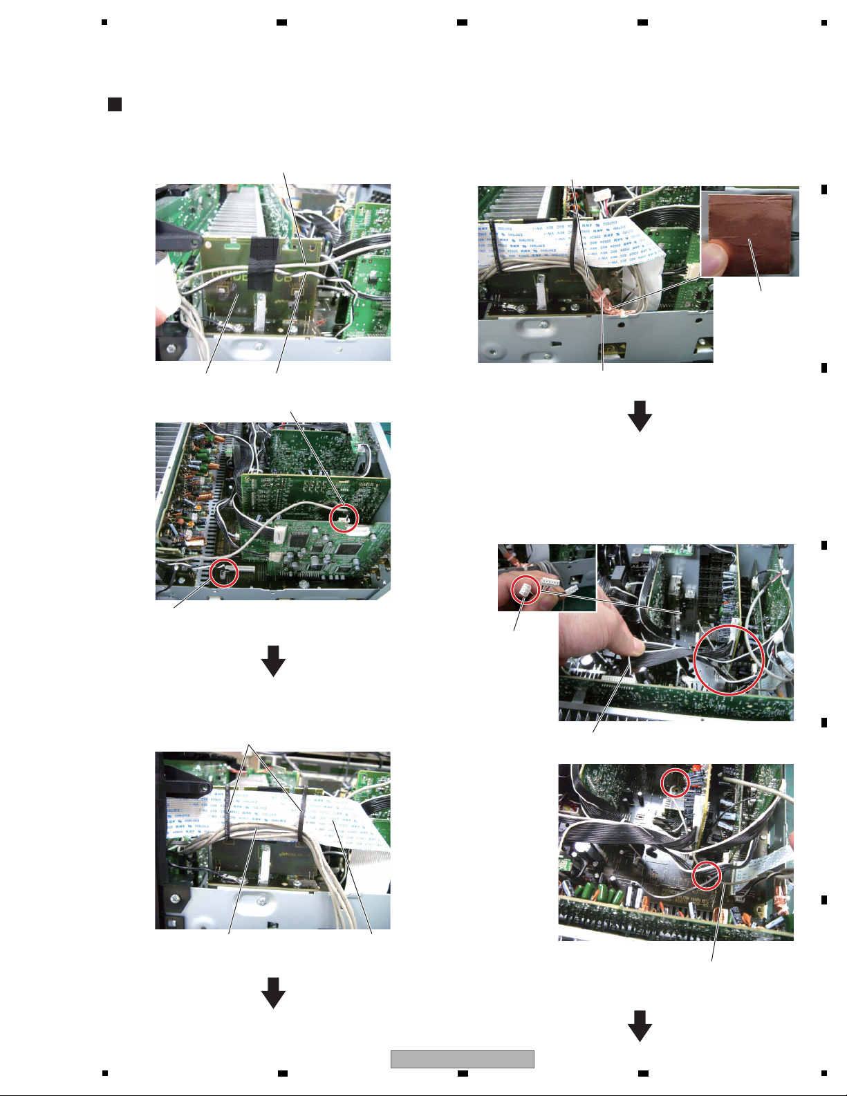
(1) Secure the wires from the USB Assy.
(4) Style the 4P wire (F-VIDEO) so that it goes below the
corresponding cables marked with circles in the figure
below.
(5) Style the remaining two wires above wire A, which
connects the AMP and INPUT Assys.
(2) Secure the card cable and the remaining wires with
the clamps.
(3) Wrap the remaining wires with CU tape foil then secure
them with a cable tie.
CABLE DRESSING (VSX-920-K)
GUIDE_R Assy
Clamp
Wire (USB <-> DSP)
Wire (USB <-> DSP)
Card cable
Wires
The remaining wires
CU tape foil
Cable tie
The 4P wire (F-VIDEO)
Wire A
Style the wires so that they
are placed above wire A.
Wire (USB <-> MAIN)
Wire (USB <-> MAIN)
4P wire
5. DISASSEMBLY
5.1 DISASSEMBLY
6 7 8
A
B
C
D
E
F
VSX-920-K
5
6 7 8
21
1
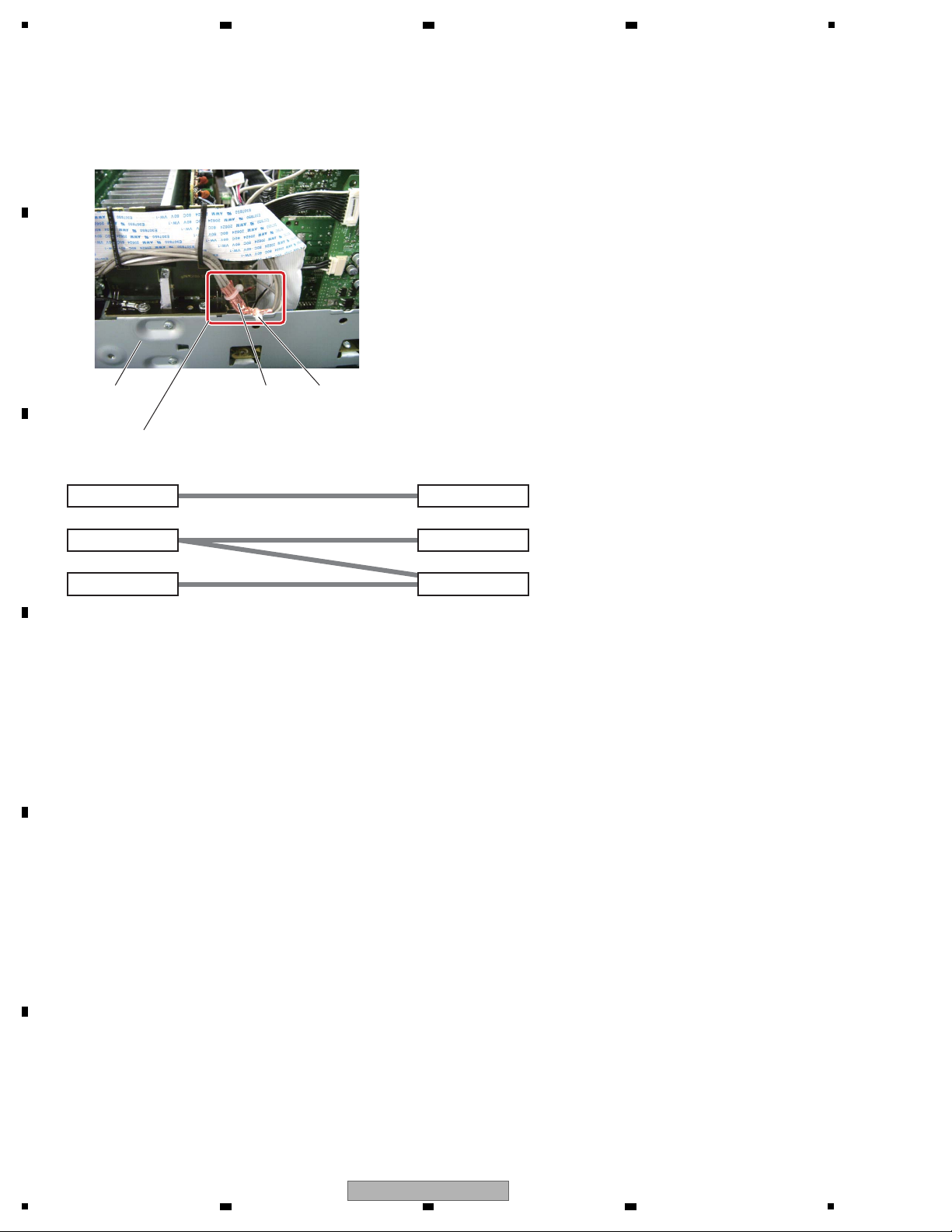
(6) Secure the cables bound with CU tape foil to the chassis,
using a cable tie for grounding.
• The wires bound with CU tape foil (part No.: 1220-21087-900-0S) are shown below.
When repairing an assy on the front side, as the wires are secured to the assys,
it is necessary to peel off CU tape foil to unbind the wires in order to disconnect them.
After repair, wrap the wires again, using new CU tape foil.
When repairing an assy on the rear side, as the wires are disconnected/connected
with connectors, you don't have to peel off CU tape foil.
After disconnecting the wires, style them again, following the procedures shown above.
Cable tie
Directly mounted wire
Chassis
USB Assy
Front side Rear side
CU tape foil
DSP Assy
Directly mounted wire
F-VIDEO Assy
VIDEO Assy
Directly mounted wire
MIC Assy
INPUT Assy
A
2 3 4
B
C
D
E
F
22
1
2 3 4
VSX-920-K
 Loading...