

Pioneer VSX-45, VSX-830-K, VSX-830-S Service Manual
2015
VSX-830-K
AV Receiver
VSX-830-K
VSX-45
VSX-830-S
THIS MANUAL IS APPLICABLE TO THE FOLLOWING MODEL(S) AND TYPE(S).
Model Type Power Requirement Remarks
VSX-830-K CUXESM AC 120 V
VSX-45 CUXE AC 120 V
VSX-830-K SYXEV8 AC 220 V to 230 V
VSX-830-S SYXEV8 AC 220 V to 230 V
ORDER NO.
RRV4594
THIS SERVICE MANUAL SHOULD BE USED TOGETHER WITH THE FOLLOWING MANUAL(S).
Model Order No. Remarks
VSX-830-K, VSX-45, VSX-830-S RRV4595 SCHEMATIC DIAGRAM, PCB CONNECTION DIAGRAM, PCB PARTS LIST
PIONEER CORPORATION 1-1, Shin-ogura, Saiwai-ku, Kawasaki-shi, Kanagawa 212-0031, Japan
PIONEER ELECTRONICS (USA) INC. P.O. Box 1760, Long Beach, CA 90801-1760, U.S.A.
PIONEER EUROPE NV Haven 1087, Keetberglaan 1, 9120 Melsele, Belgium
PIONEER ELECTRONICS ASIACENTRE PTE. LTD. 253 Alexandra Road, #04-01, Singapore 159936
PIONEER CORPORATION
K-MZV MAR.
2015 Printed in Japan
1
WARNING
This product may contain a chemical known to the State of California to cause cancer, or birth defects or other reproductive
harm.
Health & Safety Code Section 25249.6 - Proposition 65
This service manual is intended for qualified service technicians; it is not meant for the casual do-ityourselfer. Qualified technicians have the necessary test equipment and tools, and have been trained
to properly and safely repair complex products such as those covered by this manual.
Improperly performed repairs can adversely affect the safety and reliability of the product and may
void the warranty. If you are not qualified to perform the repair of this product properly and safely, you
should not risk trying to do so and refer the repair to a qualified service technician.
1. SAFETY PRECAUTIONS
The following check should be performed for the
continued protection of the customer and service
technician.
LEAKAGE CURRENT CHECK
Measure leakage current to a known earth ground
(water pipe, conduit, etc.) by connecting a leakage
current tester such as Simpson Model 229-2 or
equivalent between the earth ground and all exposed
metal parts of the appliance (input/output terminals,
screwheads, metal overlays, control shaft, etc.). Plug
the AC line cord of the appliance directly into a 120 V
AC 60 Hz outlet and turn the AC power switch on. Any
current measured must not exceed 0.5 mA.
ANY MEASUREMENTS NOT WITHIN THE LIMITS
OUTLINED ABOVE ARE INDICATIVE OF A POTENTIAL
SHOCK HAZARD AND MUST BE CORRECTED BEFORE
RETURNING THE APPLIANCE TO THE CUSTOMER.
2. PRODUCT SAFETY NOTICE
Many electrical and mechanical parts in the appliance
have special safety related characteristics. These are
often not evident from visual inspection nor the protection
afforded by them necessarily can be obtained by using
replacement components rated for voltage, wattage, etc.
Replacement parts which have these special safety
characteristics are identified in this Service Manual.
Electrical components having such features are
identified by marking with a > on the schematics and on
the parts list in this Service Manual.
The use of a substitute replacement component which
does not have the same safety characteristics as the
PIONEER recommended replacement one, shown in the
parts list in this Service Manual, may create shock, fire,
or other hazards.
Product Safety is continuously under review and new
instructions are issued from time to time. For the latest
information, always consult the current PIONEER Service
Manual. A subscription to, or additional copies of,
PIONEER Service Manual may be obtained at a nominal
charge from PIONEER.
Leakage
current
tester
Reading should
not be above
0.5 mA
Device
under
test
Test all
exposed metal
surfaces
Also test with
plug reversed
(Using AC adapter
plug as required)
Earth
ground
AC Leakage Test
(FOR USA MODEL ONLY)
2 3 4
SAFETY INFORMATION
A
B
C
D
E
F
2
1
2 3 4
VSX-830-K

5
6 7 8
CONTENTS
SAFETY INFORMATION.......................................................................................................................................................... 2
1. SERVICE PRECAUTIONS ....................................................................................................................................................4
1.1 NOTES ON SOLDERING...............................................................................................................................................4
1.2 SERVICE NOTICE.......................................................................................................................................................... 4
2. SPECIFICATIONS ................................................................................................................................................................. 5
3. BASIC ITEMS FOR SERVICE .............................................................................................................................................. 6
3.1 CHECK POINTS AFTER SERVICING ........................................................................................................................... 6
3.2 JIGS LIST ....................................................................................................................................................................... 6
3.3 PCB LOCATIONS ...........................................................................................................................................................7
4. BLOCK DIAGRAM ..............................................................................................................................................................10
4.1 OVERALL WIRING DIAGRAM .....................................................................................................................................10
4.2 AUDIO BLOCK DIAGRAM............................................................................................................................................12
4.3 DMAIN BLOCK DIAGRAM (AUDIO)............................................................................................................................. 14
4.4 DMAIN BLOCK DIAGRAM (SYSTEM) ......................................................................................................................... 16
4.5 POWER SUPPLY BLOCK DIAGRAM........................................................................................................................... 18
4.6 GND BLOCK DIAGRAM............................................................................................................................................... 20
5. DIAGNOSIS ........................................................................................................................................................................ 22
5.1 TROUBLESHOOTING..................................................................................................................................................22
5.2 CONFIMATION OF THE NETWORK MODULE ........................................................................................................... 28
5.3 ERROR INDICATIONS ................................................................................................................................................. 30
5.4 PROTECTION CIRCUIT............................................................................................................................................... 32
6. SERVICE MODE................................................................................................................................................................. 34
6.1 TEST MODE.................................................................................................................................................................34
6.2 DEFAULT SETTINGS ................................................................................................................................................... 36
7. DISASSEMBLY ................................................................................................................................................................... 37
8. EACH SETTING AND ADJUSTMENT................................................................................................................................46
8.1 ADJUSTMENT REQUIRED WHEN THE UNIT IS REPAIRED OR REPLACED .......................................................... 46
8.2 USB BACKUP...............................................................................................................................................................47
8.3 UPDATING OF THE FIRMWARE .................................................................................................................................48
8.4 IDLE CURRENT ADJUSTMENT ..................................................................................................................................51
9. EXPLODED VIEWS AND PARTS LIST............................................................................................................................... 52
1 PACKING SECTION .....................................................................................................................................................52
9.
9.2 EXTERIOR SECTION .................................................................................................................................................. 54
A
B
C
D
E
F
VSX-830-K
5
6 7 8
3

1
• For environmental protection, lead-free solder is used on the printed circuit boards mounted in this unit.
Be sure to use lead-free solder and a soldering iron that can meet specifications for use with lead-free solders for repairs
accompanied by reworking of soldering.
• Compared with conventional eutectic solders, lead-free solders have higher melting points, by approximately 40 ºC.
Therefore, for lead-free soldering, the tip temperature of a soldering iron must be set to around 373 ºC in general, although
the temperature depends on the heat capacity of the PC board on which reworking is required and the weight of the tip of
the soldering iron.
Do NOT use a soldering iron whose tip temperature cannot be controlled.
Compared with eutectic solders, lead-free solders have higher bond strengths but slower wetting times and higher melting
temperatures (hard to melt/easy to harden).
The following lead-free solders are available as service parts:
• Parts numbers of lead-free solder:
GYP1006 1.0 in dia.
GYP1007 0.6 in dia.
GYP1008 0.3 in dia.
For more detail, please refer to "7. DISASSEMBLY - 1. Discharging".
As the screw covers for the speaker terminals are subject to breakage, be careful when removing them.
If a screw cover is broken during removal, replace it with a new one.
Continuous use of a broken screw cover may cause short-circuiting of speaker terminals.
Discharging
Notice of the Parts exchange
2 3 4
1. SERVICE PRECAUTIONS
1.1 NOTES ON SOLDERING
A
B
C
D
1.2 SERVICE NOTICE
E
F
4
1
2 3 4
VSX-830-K

5
Amplifier section (VSX-830-K/CUXESM only)
Continuous average power output of 80 watts* per channel, min., at
8 ohms, from 20 Hz to 20 000 Hz with no more than 0.08 %** total
harmonic distortion.
Front (stereo)............................................................ 80 W + 80 W
Power output (1 kHz, 6 Ω, 1 %, 1 ch driven) .......................... 140 W
Guaranteed speaker impedance .................................... 6 Ω to 16 Ω
* Measured pursuant to the Federal Trade Commission’s Trade
Regulation rule on Power Output Claims for Amplifiers
** Measured by Audio Spectrum Analyzer
Audio Section (VSX-830-K/CUXESM)
Input (Sensitivity/Impedance)
LINE.........................................................................315 mV/47 kΩ
Signal-to-Noise Ratio (IHF, short circuited, A network)
LINE.................................................................................... 100 dB
Audio Section (VSX-830-K,S/SYXEV8 )
Rated power output (1 kHz, 6 Ω, 1 %)
Front, Center, Surround....................................130 W per channel
Rated power output (20 Hz to 20 kHz, 8 Ω, 0.09 %)
Front, Center, Surround....................................100 W per channel
Total harmonic distortion ....0.06 % (20 Hz to 20 kHz, 50 W/ch, 8 Ω)
Guaranteed speaker impedance .................................... 6 Ω to 16 Ω
Signal-to-Noise Ratio (IHF, short circuited, A network)
LINE.................................................................................... 100 dB
Frequency Response .......5 Hz to 100 000 Hz dB (Pure Direct Mode)
Input (Sensitivity/Impedance)
LINE.........................................................................315 mV/47 kΩ
Tuner Section
Frequency Range (FM) .................................87.5 MHz to 108 MHz
Antenna Input (FM)............................................... 75 Ω unbalanced
Frequency Range (AM) (VSX-830-K/CUXESM)........530 kHz to 1 700 kHz
Frequency Range (AM) (VSX-830-K,S/SYXEV8) .....531 kHz to 1 602 kHz
Antenna (AM) ...........................................Loop antenna (balanced)
Video Section
Signal level
Composite Video ...................................................... 1 Vp-p (75 Ω)
Bluetooth Section
Version..................................Bluetooth Specification Ver. 2.1 + EDR
Output.............................................. Bluetooth Specification Class 2
Estimated line-of-sight transmission distance* ............... About 10 m
* The line-of-sight transmission distance is an estimate. Actual
transmission distances supported may differ depending on
surrounding conditions.
Frequency range.................................................................. 2.4 GHz
Supported Bluetooth profiles ......................................A2DP, AVRCP
Supported Codec ................................SBC (Subband Codec), AAC
Digital In/Out Section
HDMI terminal .........................................................19-pin (Not DVI)
HDMI output type............................................................. 5 V, 55 mA
HDMI input/MHL terminal .............................................. 5 V, 900 mA
USB terminal .........................USB2.0 High Speed (Type A) 5 V, 1 A
iPod terminal.............................................................................. USB
Network Section (Wired)
LAN terminal............................................ 10 BASE-T/100 BASE-TX
Network Section (Wireless)
WLAN standards .............................. IEEE 802.11a, IEEE 802.11b,
IEEE 802.11g, IEEE 802.11n
Frequency band
(VSX-830-K/CUXESM, VSX-45/CUXE)
2.4 GHz band (2.412 GHz to 2.462 GHz)...........Channel 1 to Channel 11
5 GHz band (5.180 GHz to 5.240 GHz, 5.745 GHz to 5.825 GHz) ............
Channel 36 to Channel 48,
Channel 149 to Channel 165
(VSX-830-K, S/SYXEV8)
2.4 GHz band (2.412 GHz to 2.472 GHz) .......... Channel 1 to Channel 13
5 GHz band (5.180 GHz to 5.240 GHz)..........................................
Channel 36 to Channel 48
Security ......................................................Disabled (no encryption)
WEP (Key length: 64 bit/128 bit, Key format: ASCII/Hex)
WPA2 Mixed (WPA / WPA2, Encryption method: TKIP/AES,
Recognition method: PSK)
Miscellaneous
Power requirements...........AC 120 V, 60 Hz (VSX-830-K/CUXESM)
Power requirements.......................AC 220 V to 230 V, 50 Hz/60 Hz
(VSX-830-K,S/SYXEV8)
Power consumption................................................................ 450 W
In standby................................................................................ 0.1 W
In standby (HDMI control on)................................................... 0.3 W
In standby (Network standby on)............................................. 2.7 W
In standby (Network standby on, wireless LAN connected) .... 3.0 W
In standby (HDMI control on, Network standby on)................. 2.7 W
In standby (HDMI control on, Network standby on, wireless LAN
connected).......................................................................... 3.0 W
Auto power down....................... 15 min, 30 min, 60 min, off (default)
(VSX-830-K/CUXESM, VSX-45/CUXE)
15 min (default), 30 min, 60 min, off
(VSX-830-K,-S/SYXEV8)
Dimensions................... 435 mm (W) x 168 mm (H) x 331.5 mm (D)
(17 3/16 in. (W) x 6 5/8 in. (H) x 13 1/16 in. (D))
Weight (without package).....................................8.7 kg (19 lb 3 oz)
+0
-3
• MCACC Setup microphone
(APM7011)
• Remote control unit
(8300773900010S)
• AAA size IEC R03 dry cell batteries
• AM loop antenna
(E605010140010S)
• FM wire antenna
(E605010140010-IL)
• Power cord (VSX-830-K, -S/SYXEV8 only)
(L068250160070S)
• CD-ROM
(VSX-830-K/CUXESM: 6517000002141S)
(VSX-45/CUXE: 6517000002131S)
(VSX-830-K,-S/SYXEV8: 6517000002151S)
• Quick start guide
(VSX-830-K/CUXESM: 5707000009910S)
(VSX-45/CUXE: 5707000009890S)
(VSX-830-K,-S/SYXEV8: 5707000009930S)
• Safety Brochure
• Warranty sheet
Accessories
2. SPECIFICATIONS
6 7 8
A
B
C
D
E
5
6 7 8
VSX-830-K
F
5
1
10 Check the appearance of the product.
No scratches or dirt on its appearance after receiving it for service.
1 Check the firmware version. The firmware version must be the latest one.
If it is not the latest one, be sure to update it.
2 Confirm whether the customer complain has been solved.
If the customer complain occurs with the particular source, such
as Dolby Digital, DTS, AAC and HDMI, input it for the operation
check.
The customer complain must not be reappeared.
Video, Audio and operations must be normal.
5 Check a supported music file playback (e.g. wav. flac. mp3, etc).
(Make the connections with a USB memory or an iOS device)
Audio and operations including OSD output must be normal.
6 Check surround playback.
(Select Surround mode and check the multichannel operations
via the DSP circuit.)
Each channel audio and operations must be normal.
3 Check the analog audio playback.
(Make the analog connections with a CD/DVD/BD player.)
Each channel audio and operations must be normal.
7 Check the video outputs.
(Connect with a BD player.)
Video and operations must be normal.
8 Check the tuner (AM and FM) operations. Audio and operations must be normal.
9 Check the sound from headphone output. Sound must be normal, without noise.
4 Check the HDMI digital audio playback.
(Make the digital connections with a BD player.)
Each channel audio and operations must be normal.
Distortion
Noise
Volume too low
Volume too high
Volume fluctuating
Sound interrupted
See the table below for the items to be checked regarding video and audio.
No. Procedures
Item to be checked regarding audio
Block noise
Horizontal noise
Flicker
Disturbed image (video jumpiness)
Too dark
Too bright
Mottled color
Item to be checked regarding video
Check points
Items to be checked after servicing
To keep the product quality after servicing, confirm recommended check points shown below.
Diagnosis (DMAIN Assy ↔ CPU Assy)
Board to board extension jig cable (15P) GGD1848
Diagnosis (DMAIN Assy ↔ CPU Assy)
Board to board extension jig cable (9P) GGD1890
Diagnosis (DMAIN Assy ↔ CONCT Assy)
Board to board extension jig cable (7P) GGD1891
Diagnosis (DMAIN Assy ↔ CONCT Assy)
Board to board extension jig cable (15P) GGD1876
Jigs List
Jig Name Part No. Remarks
Lubricants and Glues List
Name Part No. Remarks
Silicon grease GEM1057 Refer to "9.2 EXTERIOR SECTION".
Silicon adhesive
GYA1011
(KE40RTV-W)
Refer to "9.2 EXTERIOR SECTION".
2 3 4
3. BASIC ITEMS FOR SERVICE
3.1 CHECK POINTS AFTER SERVICING
A
B
C
D
3.2 JIGS LIST
E
F
6
1
2 3 4
VSX-830-K
5
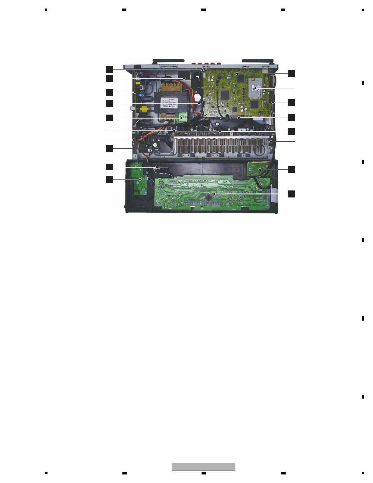
B
DMAIN ASSY
NETWORK MODULE
F
CPU ASSY
E
CONCT ASSY
G-R ASSY
H
FUSB ASSY
J
FRONT ASSY
G
AMP5 ASSY
C
OPTCO ASSY
D
SP-B ASSY
(VSX-45 only)
M
SMPS ASSY
A
MAIN ASSY
I
NTC ASSY
N
REG ASSY
K
HPMIC ASSY
L
INSEL ASSY
WG ASSY
G-L ASSY
3.3 PCB LOCATIONS
6 7 8
A
B
C
D
E
F
VSX-830-K
5
6 7 8
7
1
NOTES: - Parts marked by “NSP” are generally unavailable because they are not in our Master Spare Parts List.
-
The > mark found on some component parts indicates the importance of the safety factor of the part.
Therefore, when replacing, be sure to use parts of identical designation.
LIST OF ASSEMBLIES
VSX-830-K
/CUXESM
VSX-45
/CUXE
VSX-830-K
/SYXEV8
VSX-830-S
/SYXEV8
NSP 1..PCB TTL ASSY MAIN 7025HK1402010 7025HK1402020 7025HK1402030 7025HK1402040
2..MAIN ASSY (PCB SUB ASSY MAIN) 7028077711030 7028077711010 7028077711020 7028077711020
2..REG ASSY (PCB SUB ASSY REG) 7028077712030 7028077712010 7028077712020 7028077712020
2..CONCT ASSY (PCB SUB ASSY CONCT) 7028077713030 7028077713010 7028077713020 7028077713020
2..G-R ASSY (PCB SUB ASSY G-R) 7028077714030 7028077714010 7028077714020 7028077714020
NSP 1..PCB TTL ASSY DMAIN 7025HK1402011 7025HK1402021 7025HK1402031 7025HK1402041
2..DMAIN ASSY (PCB SUB ASSY DMAIN) 7028077771030 7028077771010 7028077771020 7028077771020
2..NETWORK MODULE AXX7293 AXX7293 AXX7293 AXX7293
NSP 1..PCB TTL ASSY FRONT 7025HK1402012 7025HK1402022 7025HK1402032 7025HK1402042
2..FRONT ASSY (PCB SUB ASSY FRONT) 7028077721050 7028077721010 7028077721040 7028077721040
2..INSEL ASSY (PCB SUB ASSY INSEL) 7028077722050 7028077722010 7028077722040 7028077722040
2..OPTCO ASSY (PCB SUB ASSY OPTCO) 7028077723050 7028077723010 7028077723040 7028077723040
2..HPMIC ASSY (PCB SUB ASSY HPMIC) 7028077724050 7028077724010 7028077724040 7028077724040
2..NTC ASSY (PCB SUB ASSY NTC) 7028077725050 7028077725010 7028077725040 7028077725040
2..G-L ASSY (PCB SUB ASSY G-L) 7028077726050 7028077726010 7028077726040 7028077726040
NSP 1..PCB TTL ASSY CPU 7025HK1402013 7025HK1402023 7025HK1402033 7025HK1402043
2..CPU ASSY (PCB SUB ASSY CPU) 7028077731050 7028077731010 7028077731040 7028077731040
2..SP-B ASSY (PCB SUB ASSY SP-B) Not used 7028077732010 Not used Not used
NSP 1..PCB TTL ASSY AMP5 7025HK1402014 7025HK1402024 7025HK1402034 7025HK1402044
2..AMP5 ASSY (PCB SUB ASSY AMP5) 7028074541040 7028074541040 7028074541040 7028074541040
2..WG ASSY (PCB SUB ASSY WG) 7028074542040 7028074542040 7028074542040 7028074542040
NSP 1..PCB TTL ASSY SMPS 7025HK1402015 7025HK1402025 7025HK1402035 7025HK1402045
> 2..SMPS ASSY (PCB SUB ASSY SMPS) 70280733610GA 70280733610GA 70280733610HA 70280733610HA
NSP 1..PCB TTL ASSY FUSB 7025HK1402016 7025HK1402026 7025HK1402036 7025HK1402046
2..FUSB ASSY (PCB SUB ASSY FUSB) 7028077781040 7028077781010 7028077781030 7028077781030
Mark Symbol and Description
A
2 3 4
B
C
D
E
F
8
1
2 3 4
VSX-830-K

5
6 7 8
A
B
C
D
E
F
VSX-830-K
5
6 7 8
9
1
B
E
E
C
B
B
C E
E
E
C
B
E
C
B
(S2) (S3)
AC-IN
(S4)
(S1)
CN403
CP1
CN3
CN9502
CX101
CX102
CX100
CN1
CN1805CP2009
CP7
CP3 CP2
CP403
CN7202B
CN3004
CN7202A
CP3501A
CN5
CP5
CP3501B
CP402
Q102FR
Q103FR
C
Q102FR
Q103
C
MAIN TRANS
VSX-45 ONLY
2SB1560
KTC3964
Q101FR
2SB1560
KTC3964
Q101FR
AC IN
2SD2390
2SD2
-
-
-
G
G G
1/2, 2/2
C
OPTCO A
(VSX-830-K
(VSX-45/CU
(VSX-830-K
D
SP-B ASSY
(7028077732010)
AMP5 A
(70280
I
NTC ASSY
(VSX-830-K/CUXESM: 7028077725050)
(VSX-45/CUXE: 7028077725010)
(VSX-830-K,-S/SYXEV8: 7028077725040)
K
HPMIC ASSY
(VSX-830-K/CUXESM: 7028077724050
(VSX-45/CUXE: 7028077724010)
(VSX-830-K,-S/SYXEV8: 70280777240
L
INSEL ASSY
(VSX-830-K/CUXESM: 7028077722050)
(VSX-45/CUXE: 7028077722010)
(VSX-830-K,-S/SYXEV8: 7028077722040)
M
SMPS ASSY
(VSX-830-K/CUXESM, VSX-45/CUXE: 70280733610GA)
(VSX-830-K,-S/SYXEV8: 70280733610HA)
N
REG ASSY
(VSX-830-K/CUXESM: 7028077712030)
(VSX-45/CUXE: 7028077712010)
(VSX-830-K,-S/SYXEV8: 7028077712020)
2 3 4
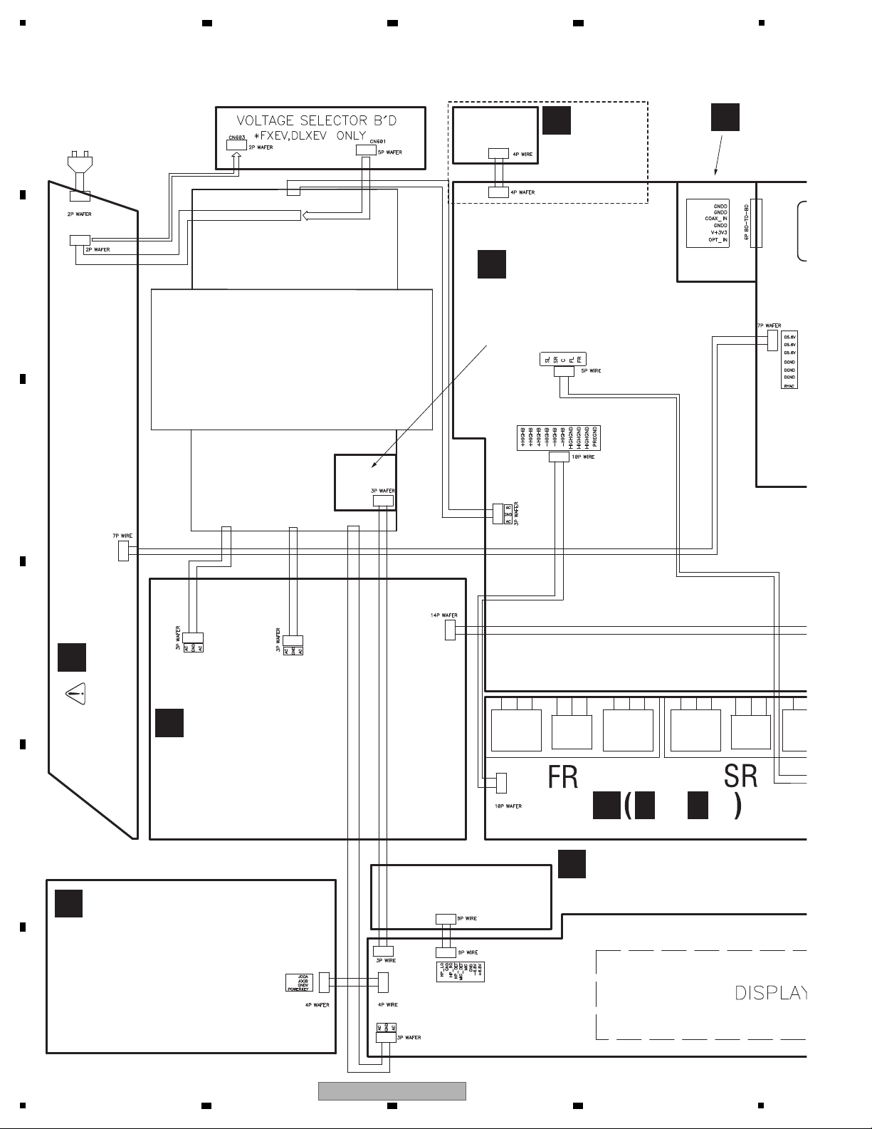
4. BLOCK DIAGRAM
4.1 OVERALL WIRING DIAGRAM
A
B
C
D
E
F
10
VSX-830-K
1
2 3 4
5
B
C E
E
B
ECB E B E
C
B
B
C
E
E
C
B
BC
AGND
V+5V
AGND
E
E
C
B
BC E
ECB
A+12V
ACWP
A-12V
CP313
CN610
CN302
CN611
CN303B
CN313B
CP312
CN312
CP311
CN311
CP310
CN310
CN9502
W7
CN2
CN602
CN301
CP113
CN114
CP114
CN113
CN105
CN1801
CN9503
CN9202
CP3601
CN314
CN308B
CP404
CN305
CN801CN802
CP3002
CN3001
CN1805CP2009
CP115
CN1
CP401
Q103FR
Q102FR
C
Q102FR
Q103FR
C
USB+12V
USB+12V
USBGND
USBGND
AGND-RLY
Q102FR
Q103FR
Q103FR
KTC3964
2SB1560
Q101FR
KTC3964
2SB1560
KTC3964
RF101QRF101Q
USB+12V
USBGND
TR+12V
2SB1560
KTC3964
Q101FR
2SD2390 2SD2390
0932DS20932DS2
TUNER PACK
-
When ordering service parts, be sure to refer to "EXPLODED VIEWS and PARTS LIST" or "PCB PARTS LIST".
-
The > mark found on some component parts indicates the impor tance of the safety factor of the part.
Therefore, when replacing, be sure to use parts of identical designation.
-
: The power supply is shown with the marked box.
CP402
CP3602
A
A A
1/2, 2/2
MAIN ASSY
(VSX-830-K/CUXESM: 7028077711030)
(VSX-45/CUXE: 7028077711010)
(VSX-830-K,-S/SYXEV8: 7028077711020)
B
B B
1/8- 8/8
DMAIN ASSY
(VSX-830-K/CUXESM: 7028077771030)
(VSX-45/CUXE: 7028077771010)
(VSX-830-K,-S/SYXEV8: 7028077771020)
C
OPTCO ASSY
(VSX-830-K/CUXESM: 7028077723050)
(VSX-45/CUXE: 7028077723010)
(VSX-830-K,-S/SYXEV8: 7028077723040)
E
CONCT ASSY
(VSX-830-K/CUXESM: 7028077713030)
(VSX-45/CUXE: 7028077713010)
(VSX-830-K,-S/SYXEV8: 7028077713020)
F
CPU ASSY
(VSX-830-K/CUXESM: 7028077731050)
(VSX-45/CUXE: 7028077731010)
(VSX-830-K,-S/SYXEV8: 7028077731040)
AMP5 ASSY
(7028074541040)
H
FUSB ASSY
(VSX-830-K/CUXESM: 7028077731050)
(VSX-45/CUXE: 7028077731010)
(VSX-830-K,-S/SYXEV8: 7028077731040)
J
FRONT ASSY
(VSX-830-K/CUXESM: 7028077721050)
(VSX-45/CUXE: 7028077721010)
(VSX-830-K,-S/SYXEV8: 7028077721040)
6 7 8
A
B
C
D
E
F
5
6 7 8
VSX-830-K
11
1
HPMIC ASSY
K
DMAIN ASSY
B
MAIN ASSY
A
BD
DVD
CD
DVD
I2S
COAX(CD)
OPT(TV)
HDMI5/MHL
HDMI3
SAT/CBL
HDMI OUT
I2S
CODEC
DIRECT
-6dB
HDMI4
SAT/CBL
HDMI RECEIVER
DSP
R-CH
Audio
Selction
ETHERNET
WIRELESS
DIGITAL IN
HDMI IN
TUNER
MIC
AXX7293
NETWORK MODULE
HDMI SWITCHER
VOLUME
AND
INPUT SELECTOR
FRONT USB
BLUETOOTH
ANALOG
INPUT
FUSB ASSY
H
IC3652
UTC4580E
IC400
BD3473KS2
SII9587
IC9601
MN864788A
IC1602
IC1801
AK4588
IC9002
D808K013DPTP400
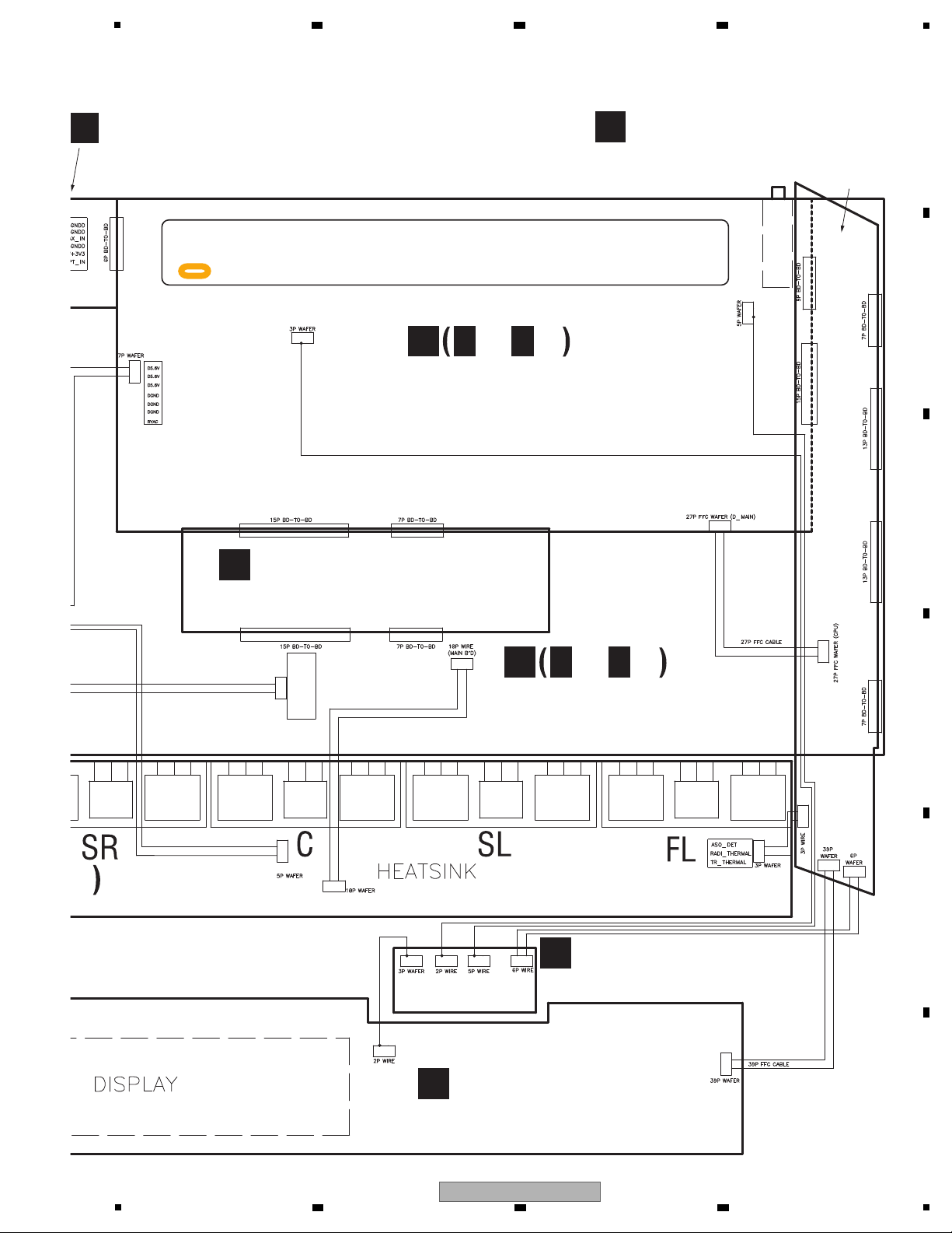
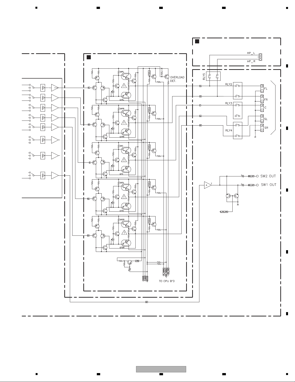
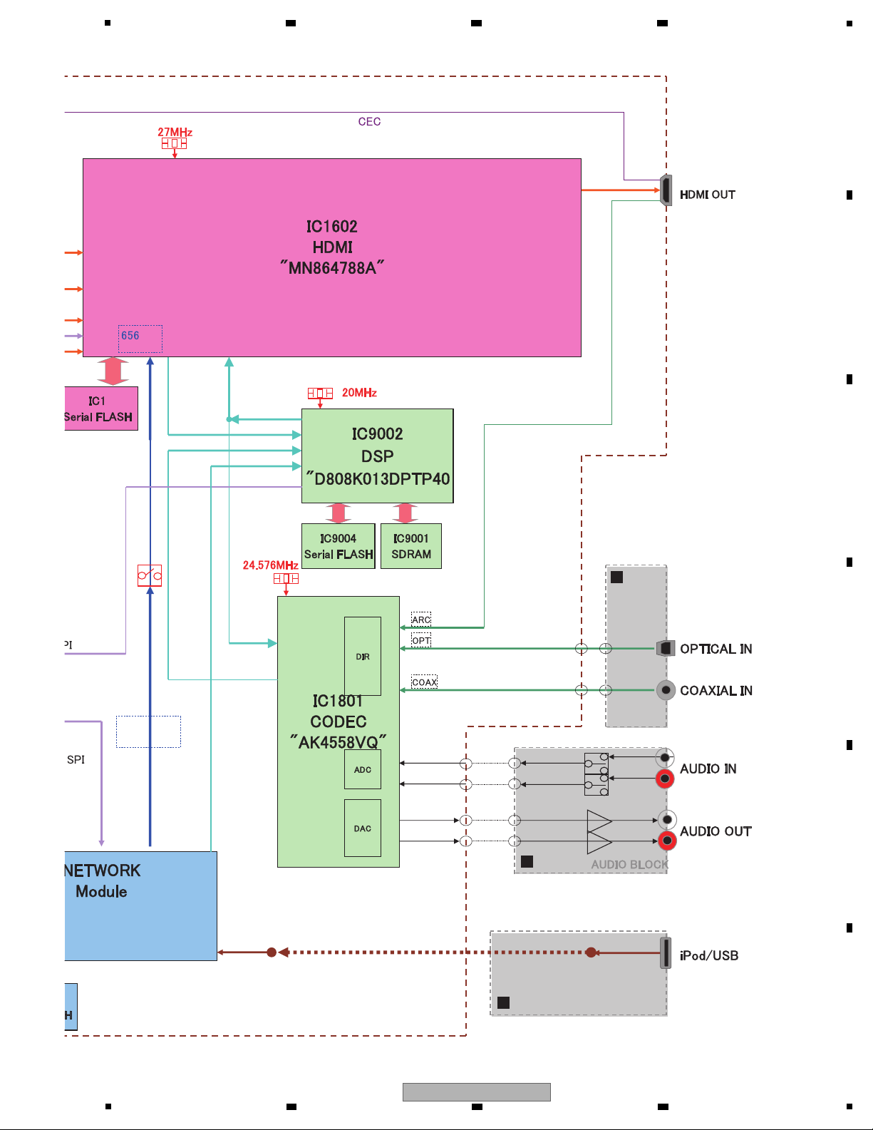
4.2 AUDIO BLOCK DIAGRAM
A
2 3 4
B
C
D
E
F
12
VSX-830-K
1
2 3 4
5
AMP5 ASSY
G
SPK OUT
HEADPHONE OUT
HPMIC ASSY
K
Q606,Q608
Q607,Q609
Q451
IC2704
NJM4580CG
6 7 8
A
B
C
D
E
F
VSX-830-K
5
6 7 8
13

1
ADC
DIR
K
E
02
COAX 1
ADDATO
DIRXAD
DIRMCKI
DIRBCK
DSD MASTER CLOCK GEN. BLOCK
NBCK
NMCK
NBCK
NBCK
CH0AMCLK
CH0ABCLK
CH1ABCLK
CH0ALRCLK
CH1ALRCLK
CH0ASD0
CH1ASD0
27.0 MHz
P1_MCLK
P1_BCK
P1_LRCK/DSDS
P1_HFDT/DSDF
P1_CDTI/DSDLFE
P1_BDTI/DSDSR
P1_SDTI/DSDC
P1_RDTI/DSDFR
D1B_BCK/P1_DSDSR
D1B_LRCK
D1BCK
AXR1[4]
AXR1[5]
AXR1[3]
AXR0[3]
AXR0[2]
AXR0[1]
AFSR0
AFSR2
AXR2[0]
ACLKR0
ACLKR2
NBCK2
HDMCK
NETMCK
NETDSDMCK
DIRMCK
24.576 MHz
XXTL0
MASTER CLOCK SELECTOR BLOC
NLRCK2
NFDAT/NDSDFL
AXR1[2]
AXR1[1]
AXR1[0]
AFSR1
ACLKR1
D1LRCK
P1B_BCK
NC_LFE
NSLR/NDSDFR
NFDAT/NDSDFL2
NLRCK2
NBCK2
CODDATO
CODLRCK
CODBCK
AXR0[9]D1SDT
AFSX0
ACLKX0
AHCLKX0
AHCLKX1
AXR0[8]D1CDT
AXR0[7]D1FDT
P1B_LRCK/DSDSL
P1B_HFDT/DSDFL
P1B_SDTI/DSD
P1B_CDTI/DSDLFE
P1B_BDTI/DSDSR
P1B_LRCK/DSDSL
P1B_RDTI/DSDFR
D1B_FDT
D1FDT
DSD_ON
D1B_FDT
6
5
12
2
9
11
3
8
D1B_BCK
D1B_LRCK
(P1_BDTI)
(P1_DSDSR)
CH0ASD1
CH0ASD2
CH0ASD3
NLRCK
NLRCK
NFDAT/NDSDF
NFDAT/NDSDF
NSLR/NDSDFR
NSLR/NDSDFR
NC_LFE
NC_LFE
DIRLRCK
DIRDATO
DIRMCK
ARCSPDIF
HDMI OUT
NETDSDMCK
DSD28X56
XTI
DAUX
IC1805
SEL(VHC157)
AND (SH08)
IC1521
AND(VHC08)
IC9003
SEL (VHC126)
IC1509
AND (VHC08)
IC1804
AND(SH08)
IC9006
VHC541
IC9101
IC9002
DSP
D808K013DPTP400
SEL (TC7SZ125)
IC8
SEL (VHC126)
IC1601
IC1511
×8 or 4
PLL
BCK2
LRCK2
SDTO2
MCKO1
OPT 1
DMAIN ASSY
B
2 3 4
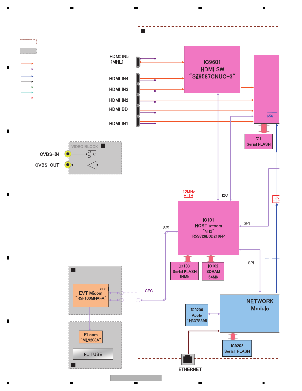
4.3 DMAIN BLOCK DIAGRAM (AUDIO)
A
B
C
ETWOR
DUL
AXX7293
16
7
D
1
2 3 4
VSX-830-K
E
F
14
D1BCK
D1LRCK
D1FDT
D1CDT
D1SDT
D1SDT(SR)
DABCK
DAMCLK
DABCK
DALRCK
DADATF
DADATC
DSPMCLKI
DALRCK
DADATF
DADATC
D1BCK
DSPPASS
H: DSP THROUGH ROUTE
L: DSP ROUTE
DSP THROUGH SELECTOR BLOCK
D1LRCK
H
L
D1FDT
D1CDT
NET
POW
DIR
POW
DAC
FL/FR
DAC
C/LFE
DAC
SL/SR
DAC
SBL/SBR
DVC
POW
76 MHz
XXTL0
ER CLOCK SELECTOR BLOCK
SDFL
20.0 MHz
: SPDIF : AMCLK : I2S : SYSCLK : FLG
: I2S BCK, LRCK
AXR0[9]D1SDT
AFSX0
ACLKX0
AHCLKX0
AHCLKX1
AXR0[8]D1CDT
AXR0[7]D1FDT
IC1510
SEL(VHC157)
AND(VHC08)
IC1804
IC1801
CODEC
AK4588
IC9002
DSP
8K013DPTP400
D1BCK
D1LRCK
D1FDT
D1CDT
D1SDT
D1SDT(SR)
DABCK
DAMCLK
DABCK
DALRCK
DADATF
DADATC
DSPMCLKI
DALRCK
DADATF
DADATC
D1BCK
DSPPASS
H: DSP THROUGH ROUTE
L: DSP ROUTE
DSP THROUGH SELECTOR BLOCK
D1LRCK
H
L
D1FDT
D1CDT
NET
POW
DIR
POW
DAC
FL/FR
DAC
C/LFE
DAC
SL/SR
DAC
SBL/SBR
DVC
POW
76 MHz
XXTL0
ER CLOCK SELECTOR BLOCK
SDFL
20.0 MHz
: SPDIF : AMCLK : I2S : SYSCLK : FLG
: I2S BCK, LRCK
AXR0[9]D1SDT
AFSX0
ACLKX0
AHCLKX0
AHCLKX1
AXR0[8]D1CDT
AXR0[7]D1FDT
IC1510
SEL(VHC157)
AND(VHC08)
IC1804
IC1801
CODEC
AK4588
IC9002
DSP
8K013DPTP400
5
6 7 8
A
B
C
D
E
F
5
6 7 8
VSX-830-K
15
1
: DMAIN ASSY
: TMDS
: CEC
: DIGITAL VIDEO
: ANALOG VIDEO/AUDIO
: SPDIF
: DIGITAL AUDIO
"AXX7293"
: CLOCK
: OTHER ASSY
DMAIN ASSY
B
MAIN ASSY
A
CPU ASSY
F
FRONT ASSY
J
2 3 4
4.4 DMAIN BLOCK DIAGRAM (SYSTEM)
A
B
C
D
E
F
16
1
2 3 4
VSX-830-K
5
"AXX7293"
MAIN ASSY
A
OPTCO ASSY
C
FUSB ASSY
H
6 7 8
A
B
C
D
E
F
VSX-830-K
5
6 7 8
17
1
(0.1UF SIZE)
10N
C118
IC100
NC
-6.8V -6.8V
IC100
C141 5600/6.3(NXA)
PC123X2YFZ
USB_+12V
V+5R6_EV
CEC
V+5V
F100
6M8(1/2W)
R100
0.1/275V
C101
1
2
4
3
LF4ZBE273H
L100
100/400(MHA)
C102
R106
120K(2W)
10
R128
1000P/1KV
C103
KIA2431AP
IC116
R133
330
C134
1N-100V
R120
4.7(1W)
6K8
R118
4K7
R112
12K-F
R109
R108
12K-F
C129
220/10(AXA)
6.8V
ZD401
6.8V
ZD400
V+5_ST
+6.8V +6.8V
V+5_ST
C109 NM
PC123X2YFZ
R111
1K
L102
10UH
CN901W
CN901B
S3(F_USB)
USB_+12V
CEC-IO
-6.8V
R116
0.68(1W)
UF4007
D119
S4(FLT)
S1(AMP B+/B-)
1500P/250V
C115
100N-K
C113
KIA7812API
ZJ16B
ZJ16B
NJM2888F33
IC305
+6.8V
A-12V1
A+12V1
AUDIO PART
C148
33/63
SARS01
D108
S2(+12V,-12V)
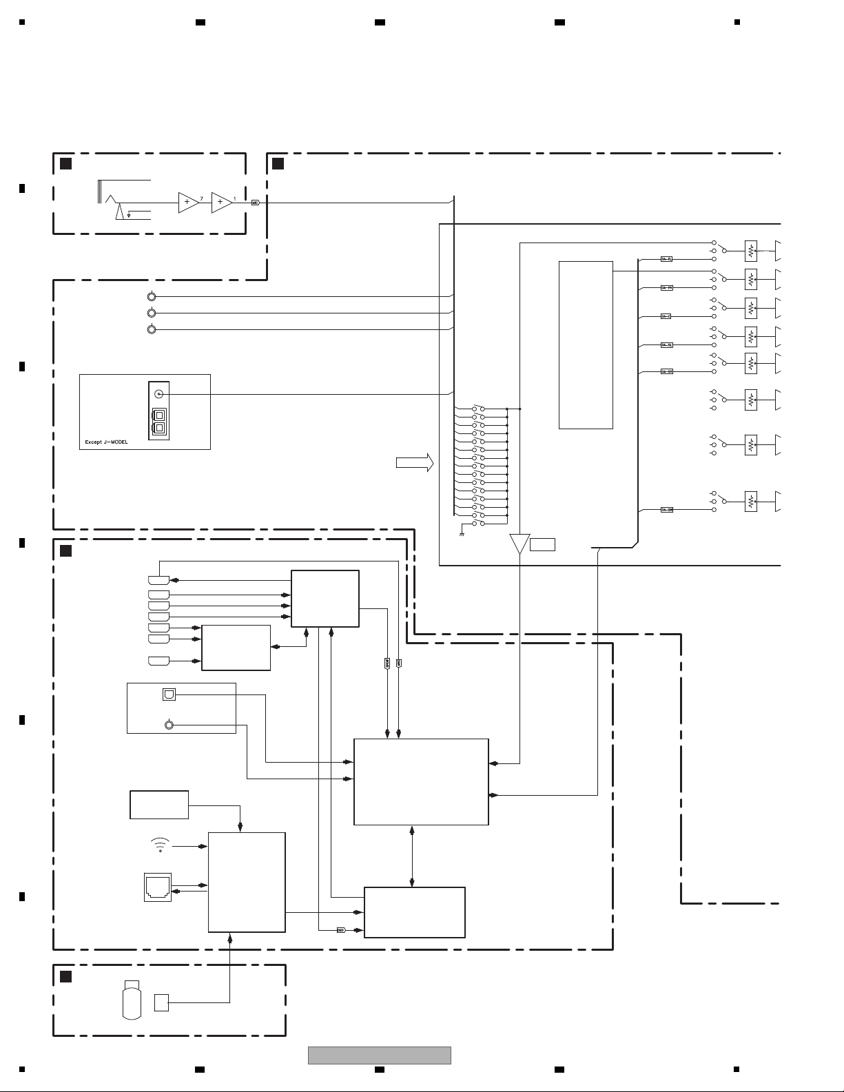
MAIN
TRANS
AC IN
S30SC6MT
D103
KIA7912PI
5
4
8
9
6
3
1
2
7
10
11
12
EE2525V
T101
KIA7805API
MAIN ASSY
A
REG ASSY
N
SMPS ASSY
M
CPU ASSY
F
2 3 4
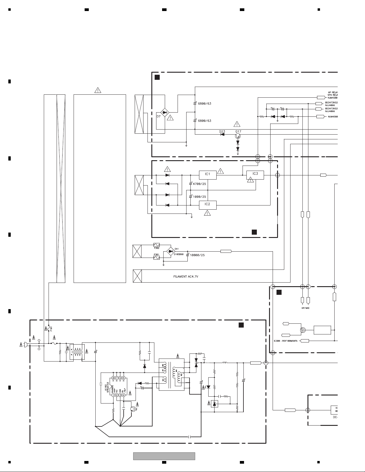
4.5 POWER SUPPLY BLOCK DIAGRAM
A
B
C
D
E
F
18
1
VSX-830-K
2 3 4
 Loading...