

2012
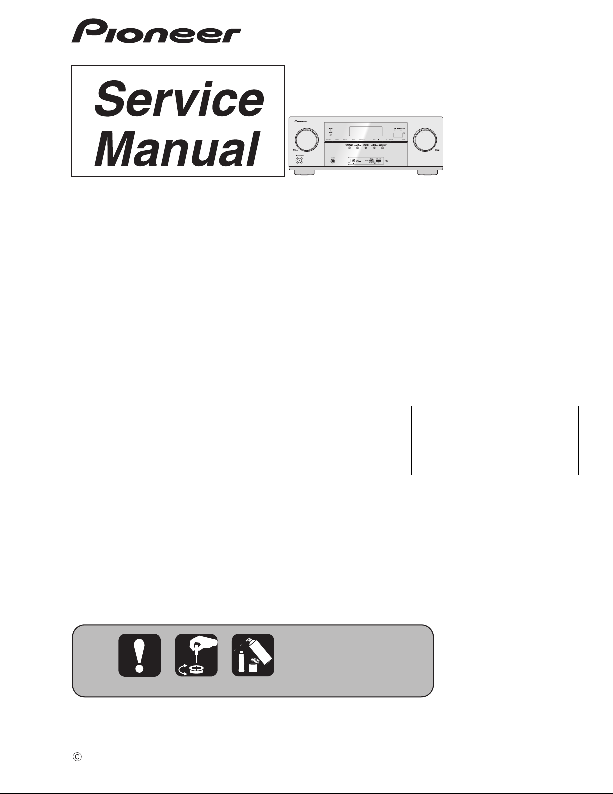
VSX-1022-K
AV Receiver
VSX-1022-K
VSX-42
VSX-822-K
THIS MANUAL IS APPLICABLE TO THE FOLLOWING MODEL(S) AND TYPE(S).
Model Type Power Requirement Remarks
VSX-1022-K CUXESM AC 120 V
VSX-42 UXECB AC 120 V
VSX-822-K CUXESM AC 120 V
ORDER NO.
RRV4306
PIONEER CORPORATION 1-1, Shin-ogura, Saiwai-ku, Kawasaki-shi, Kanagawa 212-0031, Japan
PIONEER ELECTRONICS (USA) INC. P.O. Box 1760, Long Beach, CA 90801-1760, U.S.A.
PIONEER EUROPE NV Haven 1087, Keetberglaan 1, 9120 Melsele, Belgium
PIONEER ELECTRONICS ASIACENTRE PTE. LTD. 253 Alexandra Road, #04-01, Singapore 159936
PIONEER CORPORATION
K-MZV MAR.
2012 Printed in Japan
1
WARNING
This product may contain a chemical known to the State of California to cause cancer, or birth defects or other reproductive
harm.
Health & Safety Code Section 25249.6 - Proposition 65
This service manual is intended for qualified service technicians; it is not meant for the casual do-ityourselfer. Qualified technicians have the necessary test equipment and tools, and have been trained
to properly and safely repair complex products such as those covered by this manual.
Improperly performed repairs can adversely affect the safety and reliability of the product and may
void the warranty. If you are not qualified to perform the repair of this product properly and safely, you
should not risk trying to do so and refer the repair to a qualified service technician.
1. SAFETY PRECAUTIONS
The following check should be performed for the
continued protection of the customer and service
technician.
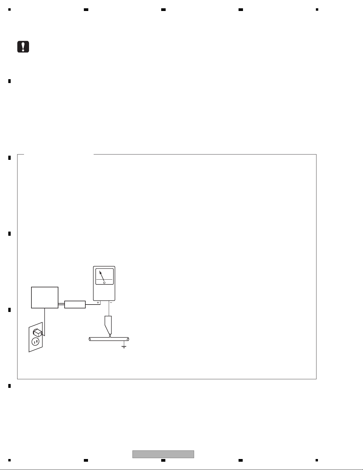
LEAKAGE CURRENT CHECK
Measure leakage current to a known earth ground
(water pipe, conduit, etc.) by connecting a leakage
current tester such as Simpson Model 229-2 or
equivalent between the earth ground and all exposed
metal parts of the appliance (input/output terminals,
screwheads, metal overlays, control shaft, etc.). Plug
the AC line cord of the appliance directly into a 120 V
AC 60 Hz outlet and turn the AC power switch on. Any
current measured must not exceed 0.5 mA.
ANY MEASUREMENTS NOT WITHIN THE LIMITS
OUTLINED ABOVE ARE INDICATIVE OF A POTENTIAL
SHOCK HAZARD AND MUST BE CORRECTED BEFORE
RETURNING THE APPLIANCE TO THE CUSTOMER.
2. PRODUCT SAFETY NOTICE
Many electrical and mechanical parts in the appliance
have special safety related characteristics. These are
often not evident from visual inspection nor the protection
afforded by them necessarily can be obtained by using
replacement components rated for voltage, wattage, etc.
Replacement parts which have these special safety
characteristics are identified in this Service Manual.
Electrical components having such features are
identified by marking with a > on the schematics and on
the parts list in this Service Manual.
The use of a substitute replacement component which
does not have the same safety characteristics as the
PIONEER recommended replacement one, shown in the
parts list in this Service Manual, may create shock, fire,
or other hazards.
Product Safety is continuously under review and new
instructions are issued from time to time. For the latest
information, always consult the current PIONEER Service
Manual. A subscription to, or additional copies of,
PIONEER Service Manual may be obtained at a nominal
charge from PIONEER.
Leakage
current
tester
Reading should
not be above
0.5 mA
Device
under
test
Test all
exposed metal
surfaces
Also test with
plug reversed
(Using AC adapter
plug as required)
Earth
ground
AC Leakage Test
(FOR USA MODEL ONLY)
2 3 4
SAFETY INFORMATION
A
B
C
D
E
F
2
1
2 3 4
VSX-1022-K

5
6 7 8
CONTENTS
SAFETY INFORMATION.......................................................................................................................................................... 2
1. SERVICE PRECAUTIONS ....................................................................................................................................................5
1.1 NOTES ON SOLDERING...............................................................................................................................................5
1.2 NOTES ON REPLACING PARTS ................................................................................................................................... 5
1.3 SERVICE NOTICE.......................................................................................................................................................... 5
2. SPECIFICATIONS ................................................................................................................................................................. 6
3. BASIC ITEMS FOR SERVICE .............................................................................................................................................. 8
3.1 CHECK POINTS AFTER SERVICING ........................................................................................................................... 8
3.2 JIGS LIST ....................................................................................................................................................................... 8
3.3 PCB LOCATIONS ...........................................................................................................................................................9
4. BLOCK DIAGRAM ..............................................................................................................................................................12
4.1 OVERALL WIRING DIAGRAM .....................................................................................................................................12
4.2 AUDIO BLOCK DIAGRAM (VSX-1022-K, VSX-42)...................................................................................................... 14
4.3 AUDIO BLOCK DIAGRAM (VSX-822-K) ...................................................................................................................... 16
4.4 D-MAIN BLOCK DIAGRAM ..........................................................................................................................................18
4.5 D-AUDIO BLOCK DIAGRAM........................................................................................................................................ 20
4.6 D-MAIN BLOCK DIAGRAM (1/2)..................................................................................................................................22
4.7 D-MAIN BLOCK DIAGRAM (2/2)..................................................................................................................................24
4.8 CPU BLOCK DIAGRAM ............................................................................................................................................... 26
4.9 VIDEO BLOCK DIAGRAM............................................................................................................................................ 28
4.10 POWER SUPPLY BLOCK DIAGRAM.........................................................................................................................30
5. DIAGNOSIS ........................................................................................................................................................................ 32
5.1 TROUBLESHOOTING..................................................................................................................................................32
5.2 ADAPTER ERROR MESSAGE ....................................................................................................................................44
5.3 USB/iPod ERROR MESSAGE......................................................................................................................................44
5.4 DETECTION CIRCUIT ................................................................................................................................................. 45
5.5 IC INFORMATION ........................................................................................................................................................ 47
6. SERVICE MODE................................................................................................................................................................. 51
6.1 SERVICE MODE ..........................................................................................................................................................51
7. DISASSEMBLY ................................................................................................................................................................... 55
8. EACH SETTING AND ADJUSTMENT................................................................................................................................64
8.1 ADJUSTMENT REQUIRED WHEN THE UNIT IS RE
8.2 UPDATING OF THE FIRMWARE .................................................................................................................................65
8.3 IDLE CURRENT ADJUSTMENT ..................................................................................................................................69
9. EXPLODED VIEWS AND PARTS LIST............................................................................................................................... 72
9.1 PACKING SECTION .....................................................................................................................................................72
9.2 EXTERIOR SECTION .................................................................................................................................................. 74
10. SCHEMATIC DIAGRAM .................................................................................................................................................... 78
10.1 AUDIO ASSY.............................................................................................................................................................. 78
10.2 AMP7 ASSY (1/2)(VSX-1022-K, VSX-42) .................................................................................................................. 80
10.3 AMP7 ASSY (2/2)(VSX-1022-K, VSX-42) .................................................................................................................. 82
10.4 AMP5 ASSY (1/2)(VSX-822-K)................................................................................................................................... 84
10.5 AMP5 ASSY (2/2)(VSX-822-K)................................................................................................................................... 86
10.6 MAIN ASSY ................................................................................................................................................................88
10.7 D-MAIN ASSY (1/7)(VSX-1022-K, VSX-42) ............................................................................................................... 90
10.8 D-MAIN ASSY (2/7)(VSX-1022-K, VSX-42) ............................................................................................................... 92
10.9 D-MAIN ASSY (3/7)(VSX-1022-K, VSX-42) ............................................................................................................... 94
10.10 D-MAIN ASSY
(4/7)(VSX-1022-K, VSX-42) .............................................................................................................96
10.11 D-MAIN ASSY (5/7)(VSX-1022-K, VSX-42) .............................................................................................................98
10.12 D-MAIN ASSY (6/7)(VSX-1022-K, VSX-42) ........................................................................................................... 100
10.13 D-MAIN ASSY (7/7)(VSX-1022-K, VSX-42) ........................................................................................................... 102
10.14 D-MAIN ASSY (1/7)(VSX-822-K)............................................................................................................................ 104
10.15 D-MAIN ASSY (2/7)(VSX-822-K)............................................................................................................................ 106
10.16 D-MAIN ASSY (3/7)(VSX-822-K)............................................................................................................................ 108
10.17 D-MAIN ASSY (4/7)(VSX-822-K)............................................................................................................................ 110
10.18 D-MAIN ASSY (5/7)(VSX-822-K)............................................................................................................................ 112
10.19 D-MAIN ASSY (6/7)(VSX-822-K)............................................................................................................................ 114
10.20 D-MAIN ASSY (7/7)(VSX-822-K)............................................................................................................................ 116
10.21 CPU ASSY..............................................................................................................................................................118
10.22 VIDEO, G-L, G-R, WG-A and WG-B ASSYS.......................................................................................................... 120
10.23 BT CNT
, OPTCO, BRG-1 and BRG-2 ASSYS........................................................................................................122
10.24 BT and F-USB ASSYS ........................................................................................................................................... 124
10.25 FRONT, INSEL, HP, MIC, FVIDEO and WG ASSYS .............................................................................................126
10.26 STBY ASSY............................................................................................................................................................128
PAIRED OR REPLACED ..........................................................64
A
B
C
D
E
F
VSX-1022-K
5
6 7 8
3

1
2 3 4
11. PCB CONNECTION DIAGRAM ......................................................................................................................................130
11.1 AUDIO ASSY ............................................................................................................................................................130
A
11.2 AMP7 ASSY (VSX-1022-K, VSX-42) ........................................................................................................................132
11.3 AMP5 ASSY (VSX-822-K) ........................................................................................................................................134
11.4 MAIN ASSY...............................................................................................................................................................136
11.5 D-MAIN ASSY...........................................................................................................................................................140
11.6 CPU ASSY ................................................................................................................................................................144
11.7 VIDEO ASSY ............................................................................................................................................................146
11.8 G-L, G-R, WG-A and WG-B ASSYS.........................................................................................................................148
11.9 BT CNT and OPTCO ASSYS ...................................................................................................................................149
11.10 BRG-1 and BRG-2 ASSYS .....................................................................................................................................150
11.11 BT and F-USB ASSYS............................................................................................................................................151
11.12 FRONT, INSEL, HP, MIC, FVIDEO and WG ASSYS ..............................................................................................152
B
11.13 STBY ASSY
12. PCB PARTS LIST ............................................................................................................................................................157
............................................................................................................................................................156
C
D
E
F
4
1
2 3 4
VSX-1022-K
5
• For environmental protection, lead-free solder is used on the printed circuit boards mounted in this unit.
Be sure to use lead-free solder and a soldering iron that can meet specifications for use with lead-free solders for repairs
accompanied by reworking of soldering.
• Compared with conventional eutectic solders, lead-free solders have higher melting points, by approximately 40 ºC.
Therefore, for lead-free soldering, the tip temperature of a soldering iron must be set to around 373 ºC in general, although
the temperature depends on the heat capacity of the PC board on which reworking is required and the weight of the tip of
the soldering iron.
Do NOT use a soldering iron whose tip temperature cannot be controlled.
Compared with eutectic solders, lead-free solders have higher bond strengths but slower wetting times and higher melting
temperatures (hard to melt/easy to harden).
The following lead-free solders are available as service parts:
• Parts numbers of lead-free solder:
GYP1006 1.0 in dia.
GYP1007 0.6 in dia.
GYP1008 0.3 in dia.
The part listed below is difficult to replace as a discrete component part.
When the part listed in the table is defective, replace whole Assy.
Assy Name
D-MAIN Assy
F-USB Assy
HDMI Connector —————— JACK with Cu-through-hole & 21 pinJA1001 - JA1007
LAN Connector —————— JACK with Cu-through-hole & 10 pinJA9202
D-MAIN 3.3V Power Supply IC —————— IC with heat-padIC9501
D-MAIN 1.2V Power Supply IC —————— IC with heat-padIC9502
D-MAIN 1.8V Power Supply IC —————— IC with heat-padIC9503
D-MAIN 3.3V Power Supply IC —————— IC with heat-padIC9504
D-MAIN 5V Power Supply IC —————— IC with heat-padIC9506
D-MAIN 5V Power Supply IC —————— IC with heat-padIC101
D-MAIN 3.3V Power Supply IC —————— IC with heat-padIC103
DSP IC —————— IC with heat-padIC1601
LAN PHY IC —————— IC with heat-padIC9203
NETWORK MEDIA PROCESSOR —————— IC BGA typeIC9204
HDMI INTERFACE IC —————— IC with heat-padIC1001
USB 5V SW IC —————— IC with heat-padIC805
USB 5V SW Power Supply IC —————— IC with heat-padIC1307
Parts that is Difficult to Replace
Ref No. Function Part No. Remarks
• Discharging
For more detail, please refer to "7. DISASSEMBLY - 1. Discharging".
• Notes on Ground Points Connection
For more detail, please refer to "7. DISASSEMBLY - 2. Notes on Ground Points Connection".
6 7 8
1. SERVICE PRECAUTIONS
1.1 NOTES ON SOLDERING
A
B
1.2 NOTES ON REPLACING PARTS
1.3 SERVICE NOTICE
5
VSX-1022-K
6 7 8
C
D
E
F
5

1
Amplifier section
Continuous average power output of 80 watts* per channel,
min., at 8 ohms, from 20 Hz to 20 000 Hz with no more than
0.08 %** total harmonic distortion.
Front (stereo)................................................... 80 W + 80 W
Power output (1 kHz, 6 Ω, 1 %) ...............140 W per channel
Guaranteed speaker impedance ........................ 6 Ω to 16 Ω
* Measured pursuant to the Federal Trade Commission’s
Trade Regulation rule on Power Output Claims for Amplifiers
** Measured by Audio Spectrum Analyzer
Audio Section
Input (Sensitivity/Impedance)
LINE.............................................................200 mV/47 kΩ
Signal-to-Noise Ratio (IHF, short circuited, A network)
LINE.......................................................................... 98 dB
Signal-to-Noise Ratio [EIA, at 1 W (1 kHz)]
LINE.......................................................................... 79 dB
Video Section
Signal level
Composite ....................................................1 Vp-p (75 Ω)
Tuner Section
Frequency Range (FM) .....................87.5 MHz to 108 MHz
Antenna Input (FM)................................... 75 Ω unbalanced
Frequency Range (AM) ...................... 530 kHz to 1700 kHz
Antenna (AM) .................................................Loop antenna
Digital In/Out Section
HDMI terminal .............................................. Type A (19-pin)
HDMI output type................................................5 V, 100 mA
USB terminal ............................USB2.0 Full Speed (Type A)
iPod terminal............................USB, and Video (Composite)
ADAPTER PORT terminal..................................5 V, 100 mA
Network Section
LAN terminal................................ 10 BASE-T/100 BASE-TX
Miscellaneous
Power Requirements ...................................AC 120 V, 60 Hz
Power Consumption ................................520 W (VSX-1022)
450 W (VSX-822)
In standby............................................. 0.4 W (Control OFF)
Dimensions....... 435 mm (W) x 168 mm (H) x 342.5 mm (D)
173/16 in. (W) x 65/8 in. (H) x 145/16 in. (D)
Weight (without package)..... 9.3 kg (20 lb 9 oz) (VSX-1022)
8.9 kg (19 lb 10 oz) (VSX-822)
Note
• Specifications and the design are subject to possible
modifications without notice, due to improvements.
• This product includes FontAvenue® fonts licensed by NEC
Corporation. FontAvenue is a registered trademark of NEC
Corporation.
VSX-1022-K, VSX-822-K
Amplifier section
Continuous average power output of 80 watts* per channel,
min., at 8 ohms, from 20 Hz to 20 000 Hz with no more than
0.08 %** total harmonic distortion.
Front (stereo)................................................... 80 W + 80 W
Guaranteed speaker impedance ........................ 6 Ω to 16 Ω
* Measured pursuant to the Federal Trade Commission’s
Trade Regulation rule on Power Output Claims for Amplifiers
** Measured by Audio Spectrum Analyzer
Audio Section
Input (Sensitivity/Impedance)
LINE.............................................................200 mV/47 kΩ
Signal-to-Noise Ratio (IHF, short circuited, A network)
LINE.......................................................................... 98 dB
Signal-to-Noise Ratio [EIA, at 1 W (1 kHz)]
LINE.......................................................................... 79 dB
Video Section
Signal level
Composite ....................................................1 Vp-p (75 Ω)
Tuner Section
Frequency Range (FM) .....................87.5 MHz to 108 MHz
Antenna Input (FM)................................... 75 Ω unbalanced
Frequency Range (AM) ...................... 530 kHz to 1700 kHz
Antenna (AM) .................................................Loop antenna
Digital In/Out Section
HDMI terminal .............................................. Type A (19-pin)
HDMI output type................................................5 V, 100 mA
USB terminal ............................USB2.0 Full Speed (Type A)
iPod terminal............................USB, and Video (Composite)
ADAPTER PORT terminal..................................5 V, 100 mA
Network Section
LAN terminal................................ 10 BASE-T/100 BASE-TX
Integrated control section
Control (IR) terminal ....................... Ø 3.5 Mini-jack (MONO)
IR signal................................ High Active (High Level: 2.0 V)
12 V Trigger terminal....................... Ø 3.5 Mini-jack (MONO)
12 V Trigger output type......................................12 V, 50 mA
Miscellaneous
Power Requirements ...................................AC 120 V, 60 Hz
Power Consumption ....................................................520 W
In standby............................................. 0.4 W (Control OFF)
Dimensions....... 435 mm (W) x 168 mm (H) x 342.5 mm (D)
173/16 in. (W) x 65/8 in. (H) x 145/16 in. (D)
Weight (without package)......................... 9.3 kg (20 lb 9 oz)
Note
• Specifications and the design are subject to possible
modifications without notice, due to improvements.
• This product includes FontAvenue® fonts licensed by NEC
Corporation. FontAvenue is a registered trademark of NEC
Corporation.
VSX-42
2. SPECIFICATIONS
A
2 3 4
B
C
D
E
F
6
1
2 3 4
VSX-1022-K
5
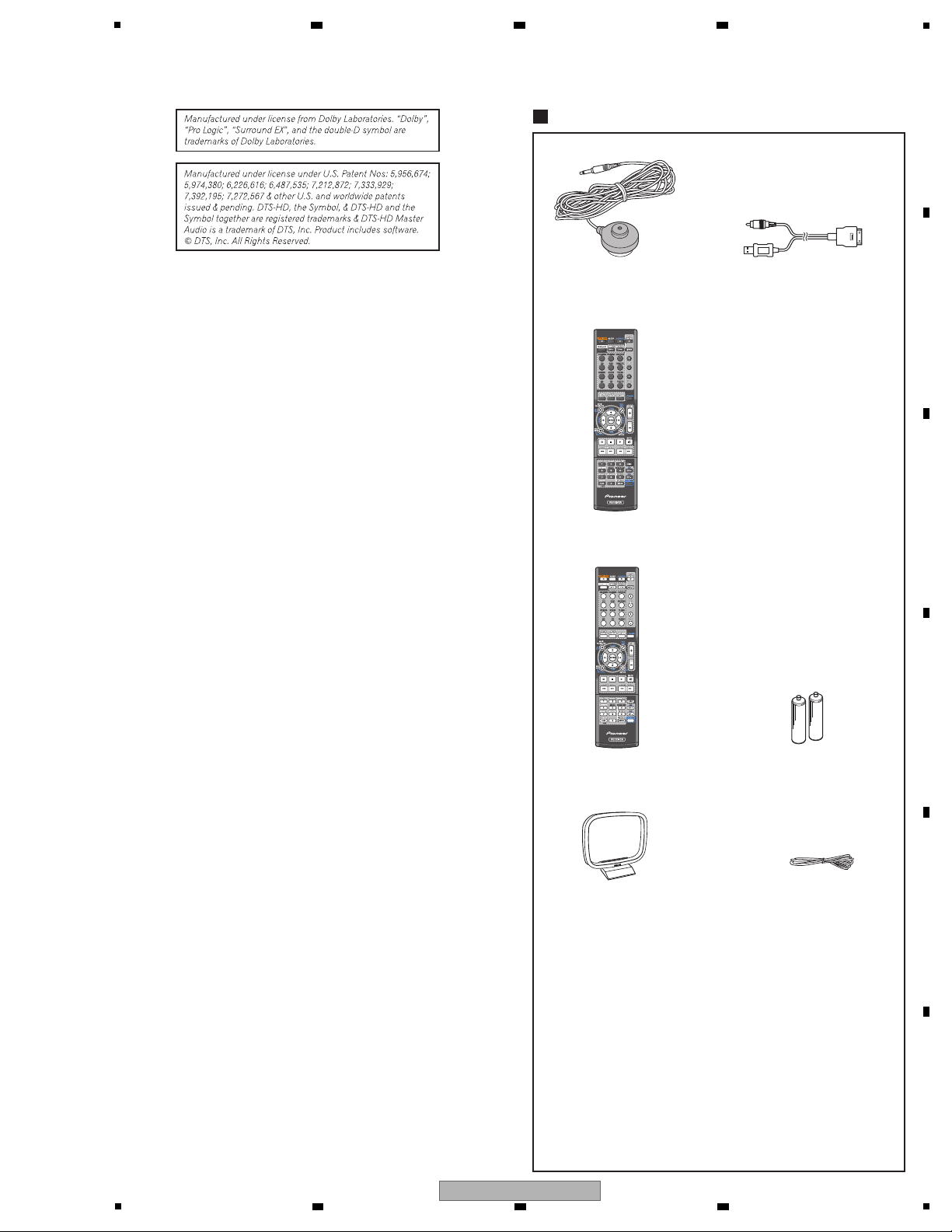
Accessories
Remote control (AXD7661)
(VSX-1022-K, VSX-822-K: 8300766100010-IL)
Remote control (AXD7662)
(VSX-42: 8300766200010-IL)
AM loop antenna
(E601019000010-IL)
Warranty card
Quick start guide
(VSX-1022-K: 5707000006490-IL)
(VSX-42: 5707000006500-IL)
(VSX-822-K: 5707000006490-IL)
Safety Brochure
Operating instructions (CD-ROM)
(VSX-1022-K, VSX-822-K: 6517000000490-IL)
(VSX-42: 6517000000510-IL)
FM wire antenna
(E605010140010-IL)
Dry cell batteries
(AAA size IEC R03) x2
Microphone
(for Auto MCACC setup)
(APM7010)
iPod cable
(L308102013030-IL)
6 7 8
A
B
C
D
E
F
VSX-1022-K
5
6 7 8
7
1
Items to be checked after servicing
To keep the product quality after servicing, confirm recommended check points shown below.
See the table below for the items to be checked regarding video and audio.
No.
Item to be checked regarding video Item to be checked regarding audio
Procedures Check points
1 Confirm whether the customer complain has been solved.
If the customer complain occurs with the particular source, such
as Dolby Digital, DTS, AAC, DVD-A and HDMI, input it for the
operation check.
The customer complain must not be reappeared.
Video, Audio and operations must be normal.
2 Check the analog audio playback.
(Make the analog connections with a DVD player.)
Each channel audio and operations must be normal.
3 Check the digital audio playback.
(Make the digital connections with a DVD player.)
Each channel audio and operations must be normal.
4 Check surround playback.
(Select Surround mode and check the multichannel operations
via the DSP circuit.)
Each channel audio and operations must be normal.
5 Check the video outputs.
(Connect with a DVD player.)
Video and operations must be normal.
6 Check the tuner (AM and FM) operations. Audio and operations must be normal.
7 Check the sound from headphone output. Sound must be normal, without noise.
8 Check the appearance of the product.
Block noise Distortion
Horizontal noise Noise
Flicker Volume too low
Disturbed image (video jumpiness) Volume too high
Too dark Volume fluctuating
Too bright Sound interrupted
Mottled color
No scratches or dirt on its appearance after receiving it for
service.
Jigs List
Jig Name Part No. Remarks
RS-232C update jig (Jig + 10P FFC) GGF1642
(Marketing product)
MAIN microcomputer firmware update
(RS-232C ↔ Rear panel)
RS-232C cable (9-pin to 9-pin, straight cable)
9P extension jig cable GGD1739 Diagnosis (AMP5 Assy ↔ AUDIO Assy)
13P extension jig cable GGD1740 Diagnosis (AMP7 Assy ↔ AUDIO Assy)
3P extension jig cable GGD1741 Diagnosis (AMP7 Assy ↔ MAIN Assy)
Diagnosis (D-MAIN Assy ↔ CPU Assy)Board to board extension jig cable GGD1770
Diagnosis (D-MAIN Assy ↔ CPU Assy)Board to board extension jig cable GGD1800
Diagnosis (FRONT Assy ↔ CPU Assy)25P extension jig FFC GGD1801
Diagnosis (D-MAIN Assy ↔ BRG-A Assy)Board to board extension jig cable GGD1756
Lubricants and Glues List
Name Part No. Remarks
Silicon grease GEM1057 Refer to "9.2 EXTERIOR SECTION".
Silicon adhesive
GYA1011
(KE40RTV-W)
Refer to "9.2 EXTERIOR SECTION".
2 3 4
3. BASIC ITEMS FOR SERVICE
3.1 CHECK POINTS AFTER SERVICING
A
B
C
D
3.2 JIGS LIST
E
F
8
1
2 3 4
VSX-1022-K
5
N
BRG-2 ASSY
M
BRG-1 ASSY
H
G-R ASSY
E
CPU ASSY
I
WG-A ASSY
P
F-USB ASSY
Q
FRONT ASSY
V
WG ASSY
A
AUDIO ASSY
O
BT ASSY
L
OPT CO ASSY
D
D-MAIN ASSY
C
MAIN ASSY
U
FVIDEO ASSY
T
MIC ASSY
K
BT CNT ASSY
B
AMP7 ASSY
/ AMP5 ASSY
J
WG-B ASSY
F
VIDEO ASSY
G
G-L ASSY
W
STBY ASSY
R
INSEL ASSY
S
HP ASSY
3.3 PCB LOCATIONS
6 7 8
A
B
C
D
E
F
VSX-1022-K
5
6 7 8
9
1
LIST OF ASSEMBLIES
NOTES: - Parts marked by “NSP” are generally unavailable because they are not in our Master Spare Parts List.
-
The > mark found on some component parts indicates the importance of the safety factor of the part.
Therefore, when replacing, be sure to use parts of identical designation.
Mark Symbol and Description
VSX-1022-K/
CUXESM
1..PCB TTL ASSY MAIN 7025HK1108010-IL
2..MAIN ASSY 7028071611030-IL
2..BTCNT ASSY 7028071612050-IL
2..OPTCO ASSY 7028071613050-IL
2..G-R ASSY 7028071614050-IL
2..G-L ASSY 7028071615050-IL
2..WG-A ASSY 7028071616050-IL
VSX-42/
UXECB
VSX-822-K/
CUXESM
2..WG-B ASSY 7028071617050-IL
7025HK1108020-IL
7028071611050-IL
7028071612050-IL
7028071613050-IL
7028071614050-IL
7028071615050-IL
7028071616050-IL
7028071617050-IL
7025HK1107010-IL
7028071611010-IL
7028071612050-IL
7028071613050-IL
7028071614050-IL
7028071615050-IL
7028071616050-IL
7028071617050-IL
NSP
1.PCB TTL ASSY FRONT 7025HK1108011-IL
2..FRONT ASSY 7028071621030-IL
2..HP ASSY 7028071622030-IL
2..INSEL ASSY 7028071623030-IL
2..MIC ASSY 7028071624050-IL
2..FVIDEO ASSY 7028071626030-IL
2..WG ASSY 7028071627060-IL
7025HK1108021-IL
7028071621050-IL
7028071622050-IL
7028071623050-IL
7028071624050-IL
7028071626050-IL
7028071627060-IL
7025HK1108011-IL
7028071621030-IL
7028071622030-IL
7028071623030-IL
7028071624050-IL
7028071626030-IL
7028071627060-IL
NSP
1..PCB TTL ASSY VIDEO 7025HK1108012-IL
2..VIDEO ASSY 7028071671030-IL
2..STBY ASSY 7028071672030-IL
2..BRG-1 ASSY 7028071673030-IL
2..BRG-2 ASSY 7028071674030-IL
7025HK1108022-IL
7028071671030-IL
7028071672030-IL
7028071673030-IL
7028071674050-IL
7025HK1107012-IL
7028071671010-IL
7028071672010-IL
7028071673030-IL
7028071674030-IL
NSP
1..PCB TTL ASSY AUDIO 7025HK1108013-IL
2..AUDIO ASSY 7028071641030-IL
7025HK1108023-IL
7028071641050-IL
7025HK1107013-IL
7028071641010-IL
NSP
1..PCB TTL ASSY DMAIN 7025HK1108014-IL
2..D-MAIN ASSY 7028071691050-IL
7025HK1108024-IL
7028071691050-IL
7025HK1107014-IL
7028071691010-IL
NSP
1..PCB TTL ASSY CPU 7025HK1108015-IL
2..CPU ASSY 7028071681030-IL
7025HK1108025-IL
7028071681050-IL
7025HK1107015-IL
7028071681010-IL
NSP
1..PCB TTL ASSY BT 7025HK1009019-IL
2..BT ASSY 7028070231010-IL
7025HK1009019-IL
7028070231010-IL
7025HK1009019-IL
7028070231010-IL
NSP
1..PCB TTL ASSY F-USB 7025HK1108016-IL
2..F-USB ASSY 7028071781030-IL
7025HK1108016-IL
7028071781030-IL
7025HK1108016-IL
7028071781030-IL
NSP
1..PCB TTL ASSY AMP7 7025HK1108017-IL
2..AMP7 ASSY 7028070253010-IL
7025HK1108017-IL
7028070253010-IL
Not used
Not used
NSP
1..PCB TTL ASSY AMP5 Not used
2..AMP5 ASSY Not used
Not used
Not used
7025HK1107017-IL
7028070245010-IL
NSP
A
2 3 4
B
C
D
E
F
10
VSX-1022-K
1
2 3 4

5
6 7 8
A
B
C
D
E
F
VSX-1022-K
5
6 7 8
11
1
-
When ordering service parts, be sure to refer to "EXPLODED VIEWS and PARTS LIST" or "PCB PARTS LIST".
-
The > mark found on some component parts indicates the impor tance of the safety factor of the part.
Therefore, when replacing, be sure to use parts of identical designation.
A
AUDIO ASSY
(VSX-1022-K: 7028071641030-IL)
(VSX-42: 7028071641050-IL)
(VSX-822-K: 7028071641010-IL)
C
MAIN ASSY
(VSX-1022-K: 7028071611030-IL)
(VSX-42: 7028071611050-IL)
(VSX-822-K: 7028071611010-IL)
F
VIDEO ASSY
(VSX-1022-K, VSX-42: 7028071671030-IL)
(VSX-822-K: 7028071671010-IL)
N
BRG-2 ASSY
(VSX-1022-K, VSX-822-K: 7028071674030-IL)
(VSX-42: 7028071674050-IL)
I
WG-A ASSY
(7028071616050-IL)
J
WG-B ASSY
(7028071617050-IL)
V
WG ASSY
(7028071627060-IL)
M
BRG-1 ASSY
(7028071673030-IL)
G
G-L ASSY
(7028071615050-IL)
K
BTCNT ASSY
(7028071612050-IL)
O
BT ASSY
(7028070231010-IL)
S
HP ASSY
(VSX-1022-K, VSX-822-K:
7028071622030-IL)
(VSX-42: 7028071622050-IL)
U
FVIDEO ASSY
(VSX-1022-K, VSX-822-K:
7028071626030-IL)
(VSX-42: 7028071626050-IL)
T
MIC ASSY
(7028071624050-IL)
H
G-R ASSY
(7028071614050-IL)
B
B
1/2-B2/2
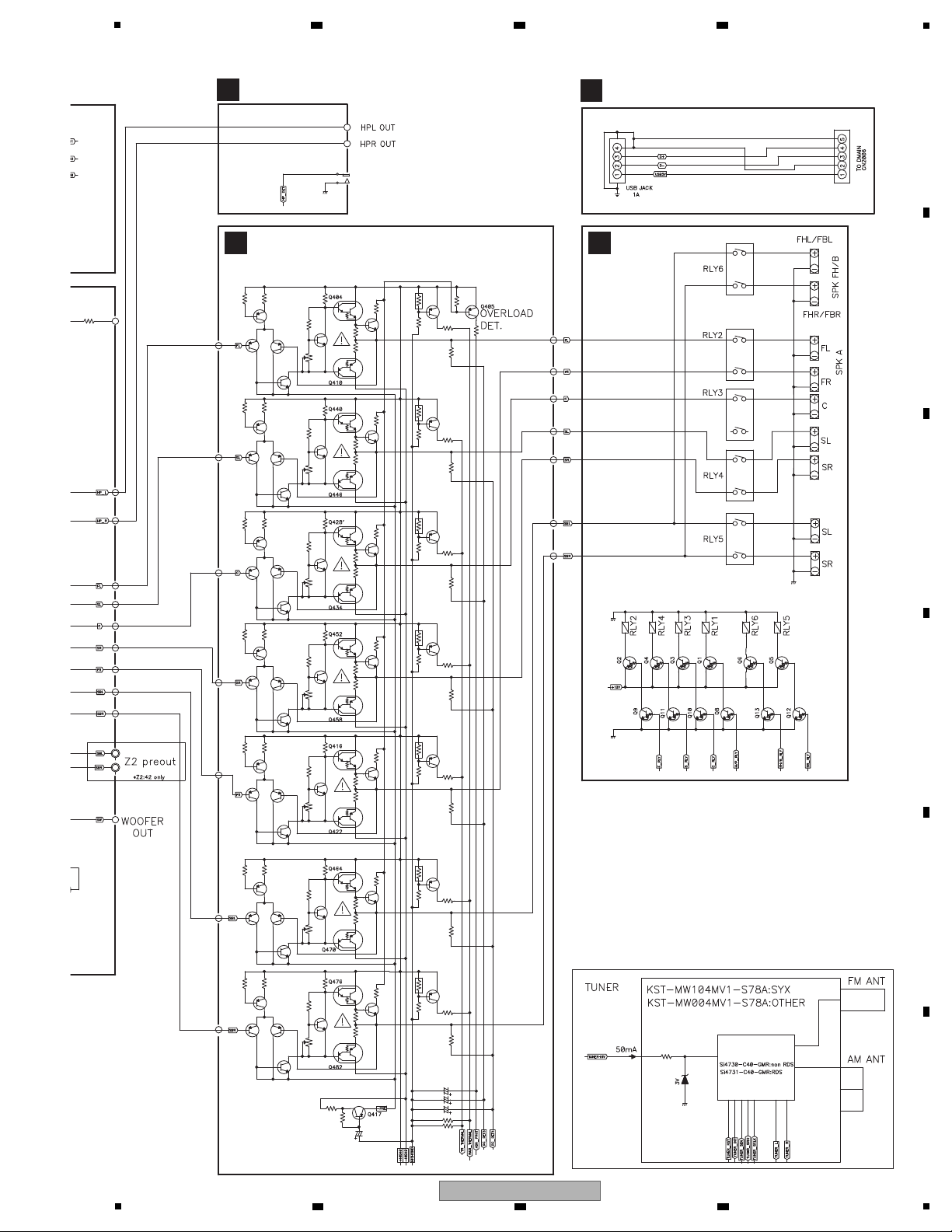
AMP7 ASSY (VSX-1022-K, VSX-42)
(7028070253010-IL)
AMP5 ASSY (VSX-822-K)
(7028070245010-IL)
CN403
1 BT_R
2 AGND
3 BT_L
4 CPU_GND
5 BT_ON/CE
6 BT_+5V
7 BT_ID
8 BT_DET
9 BT_TX/U_RX
10 BT_RX/U_TX
11 BT_/OC
BT_R 1
AGND 2
BT_L 3
CPU_GND 4
BT_ON/CE 5
BT_+5V 6
BT_ID 7
BT_DET 8
BT_TX/U_RX 9
BT_RX/U_TX 10
BT_/OC 11
11
12
13
14
15
16
17
18
19
11
12
13
14
15
16
17
18
19
2 3 4
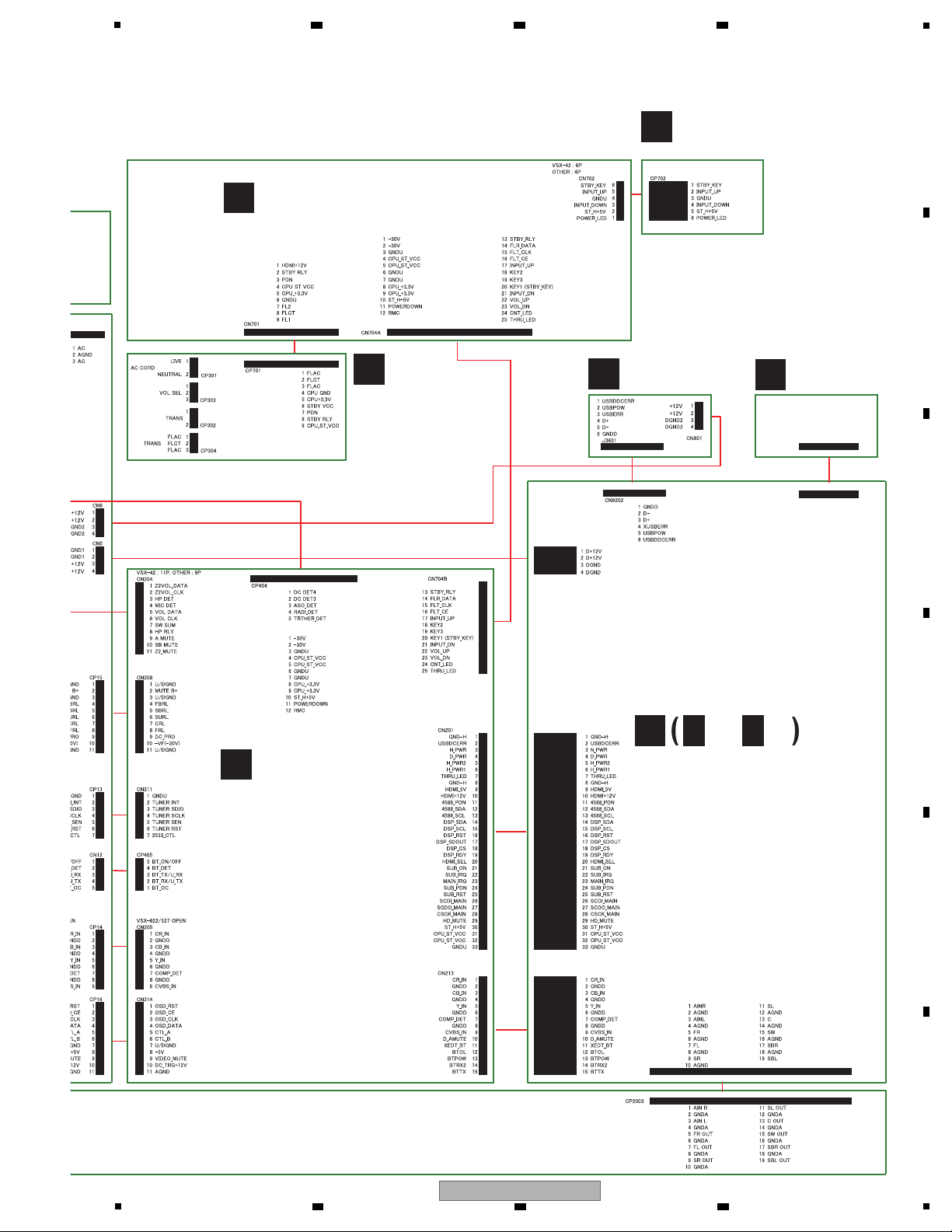
4. BLOCK DIAGRAM
4.1 OVERALL WIRING DIAGRAM
A
B
C
D
E
F
12
VSX-1022-K
1
2 3 4
5
D
D
1/7-D7/7
D-MAIN ASSY
(VSX-1022-K, VSX-42: 7028071691050-IL)
(VSX-822-K: 7028071691010-IL)
W
STBY ASSY
(VSX-1022-K, VSX-42:
7028071672030-IL)
(VSX-822-K:
7028071672010-IL)
Q
FRONT ASSY
(VSX-1022-K, VSX-822-K: 7028071621030-IL)
(VSX-42: 7028071621050-IL)
P
F-USB ASSY
(7028071781030-IL)
R
INSEL ASSY
(VSX-1022-K, VSX-822-K: 7028071623030-IL)
(VSX-42: 7028071623050-IL)
-IL)
L
OPTCO ASSY
(7028071613050-IL)
E
CPU ASSY
(VSX-1022-K: 7028071681030-IL)
(VSX-42: 7028071681050-IL)
(VSX-822-K: 7028071681010-IL)
CN2009
1 OPT
2 V+3.3
3 GND
4 COAX
5 GND
6 V+5HD
7 232TX
8 232RX
8 OPT IN
7 V+3R3
6 GNDD
5 COAX IN
4 GNDD
3 V+5_HD
2 232TX
1 232RX
CN1402
CN1401
CN9501
CN102
CN101
6 7 8
A
B
C
D
5
VSX-1022-K
6 7 8
E
F
13
1
P
F-USB ASSY
Q
FRONT ASSY
A
AUDIO ASSY
O
BT ASSY
U
FVIDEO ASSY
T
MIC ASSY
UTC4580
UTC4580
UTC4580
UTC4580
UTC4580
UTC4580
2 3 4
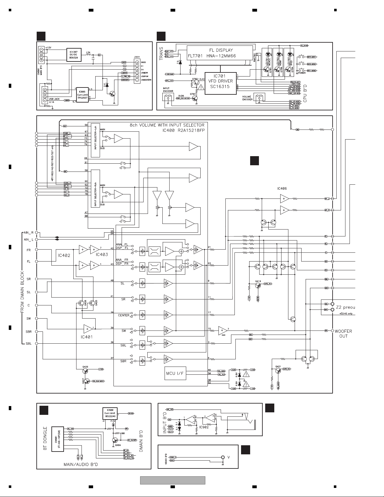
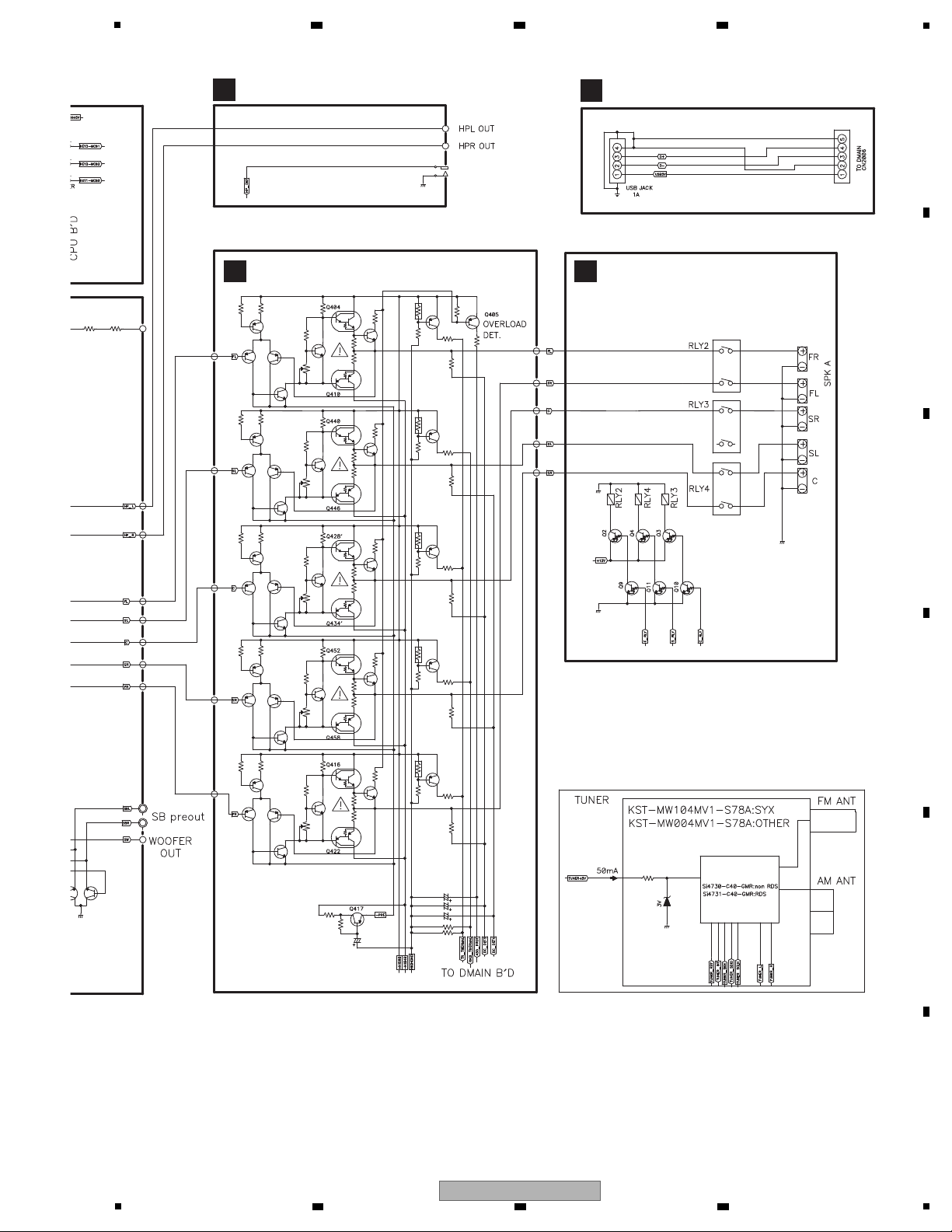
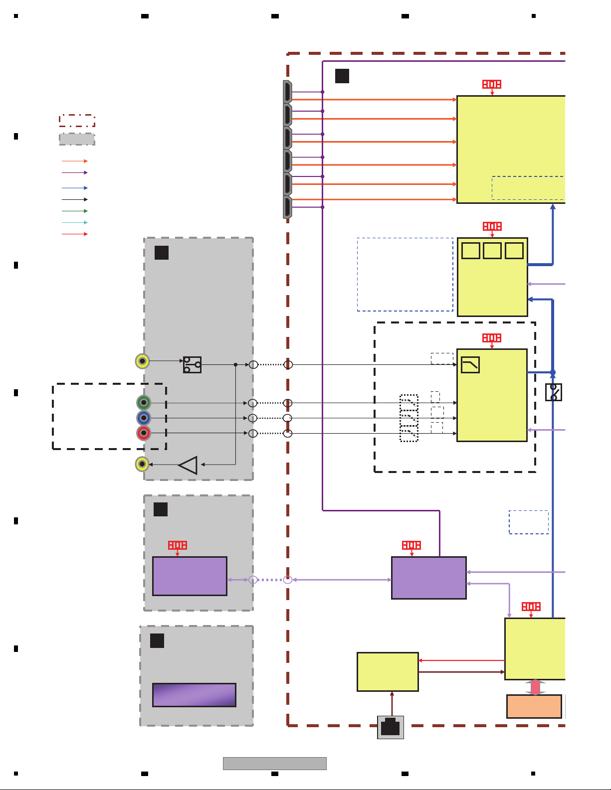
4.2 AUDIO BLOCK DIAGRAM (VSX-1022-K, VSX-42)
A
B
C
D
E
F
14
VSX-1022-K
1
2 3 4
5
S
HP ASSY
C
MAIN ASSY
B
AMP7 ASSY
P
F-USB ASSY
6 7 8
A
B
C
D
E
F
VSX-1022-K
5
6 7 8
15
1
1 2 3 4 5 6
J3601
A
AUDIO ASSY
Q
FRONT ASSY
T
MIC ASSY
P
F-USB ASSY
O
BT ASSY
U
FVIDEO ASSY
UTC4580
UTC4580
UTC4580
UTC4580
UTC4580
UTC4580
2 3 4
4.3 AUDIO BLOCK DIAGRAM (VSX-822-K)
A
B
C
D
E
F
16
VSX-1022-K
1
2 3 4
5
S
HP ASSY
C
MAIN ASSY
Y
B
AMP5 ASSY
P
F-USB ASSY
6 7 8
A
B
C
D
E
F
VSX-1022-K
5
6 7 8
17
1
VSX - 1022/42/827 only
IC 1202
Video
Decoder
"ADV7181C"
IC 102
Sub Micom
" uPD78F 1167AGF
IC 1203
IP.SC A LER
"ABT1015"
28.63636MHz
27MHz
27MHz
HDMI GAME_IN
HDMI DVD_IN
HDMI SAT/ CBL_IN
HDMI BD_IN
CVBS-IN
other ASSY
20MHz
IP ADJ . SC
TMDS
DIGITAL VIDEO
SPDIF
ANALOG VIDEO/AUDIO
CLOCK
DIGITAL AUDIO
More than VDEC 480p
output
CK:27M- 74.25MHz
/DT:20bit/DE,VS,HS
Only VDEC 480i output
MA IN Micom
" R5F 3650KNFA"
16MHz
FL TUBE
CVBS-OUT
SPI
Y
Cb
CVBS
Cr
COMPONENT-IN
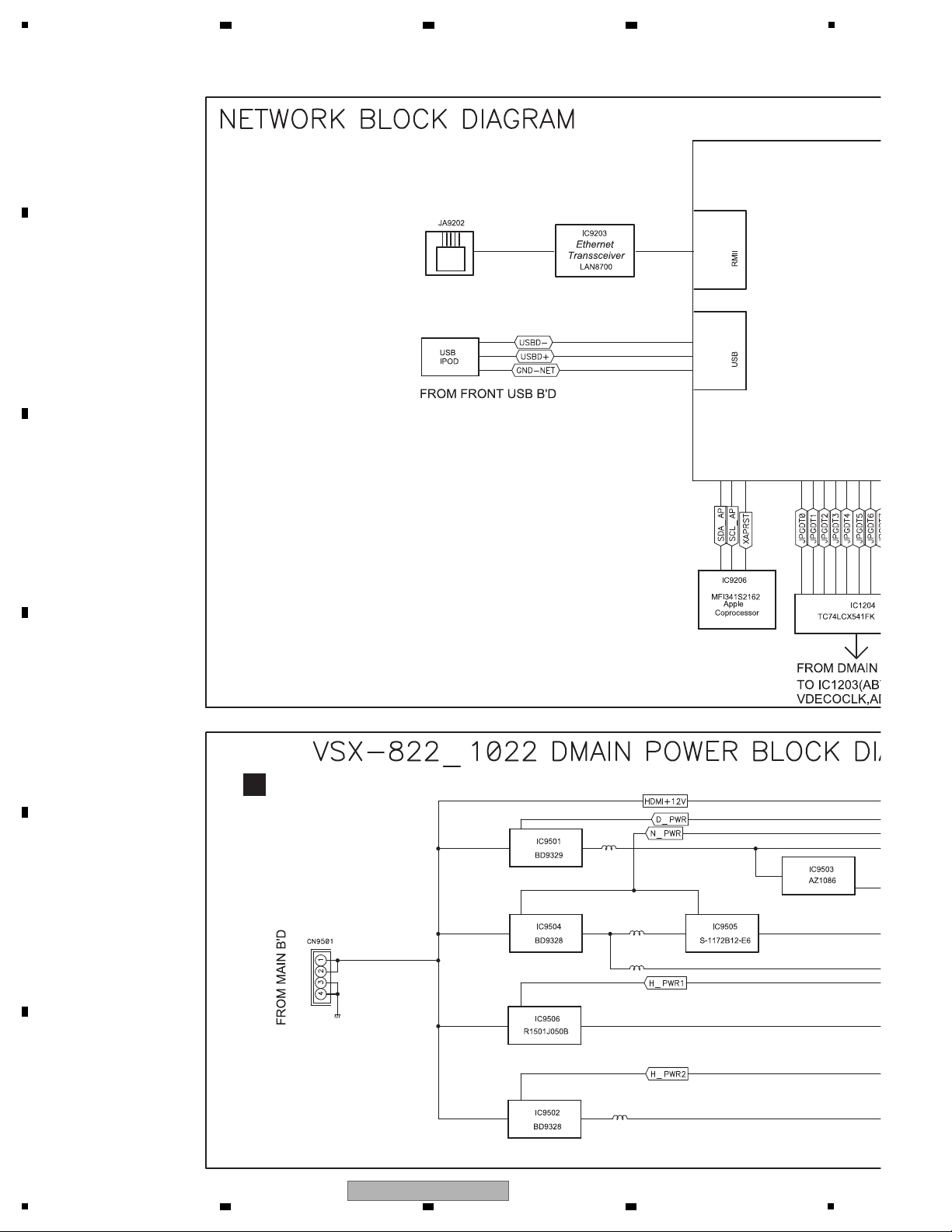
IC 9203
LAN PHY
IC 92
NETW
"DM8
NAND
24MHz
ETHERNET
25MHz
SPI
Only
HDMI DVR/ BDR_IN
HDMI VIDEO_IN
I2C
VSX - 1022/42/827 only
CK:27M- 148.5MHz
CEC
CEC
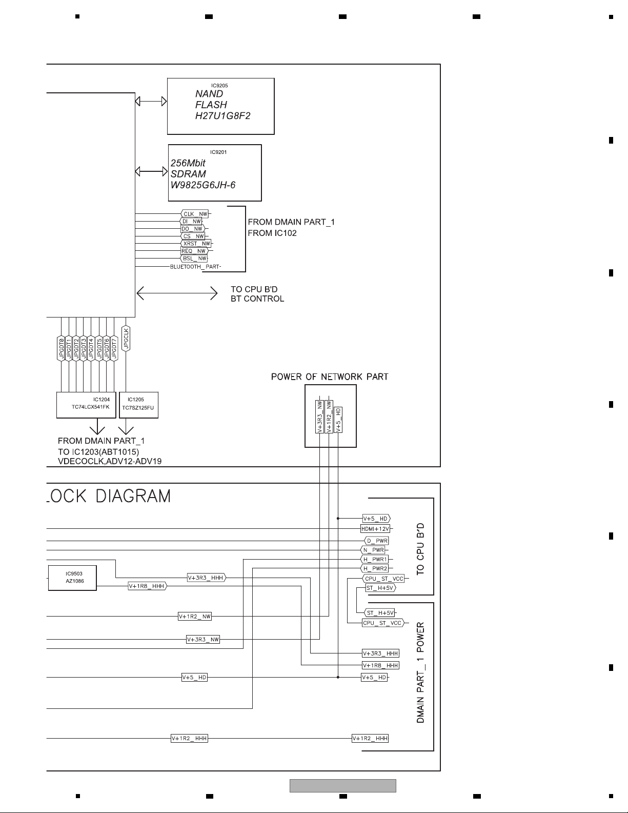
D-MAIN ASSY
D
D-MAIN ASSY
F
VIDEO ASSY
E
CPU ASSY
Q
FRONT ASSY
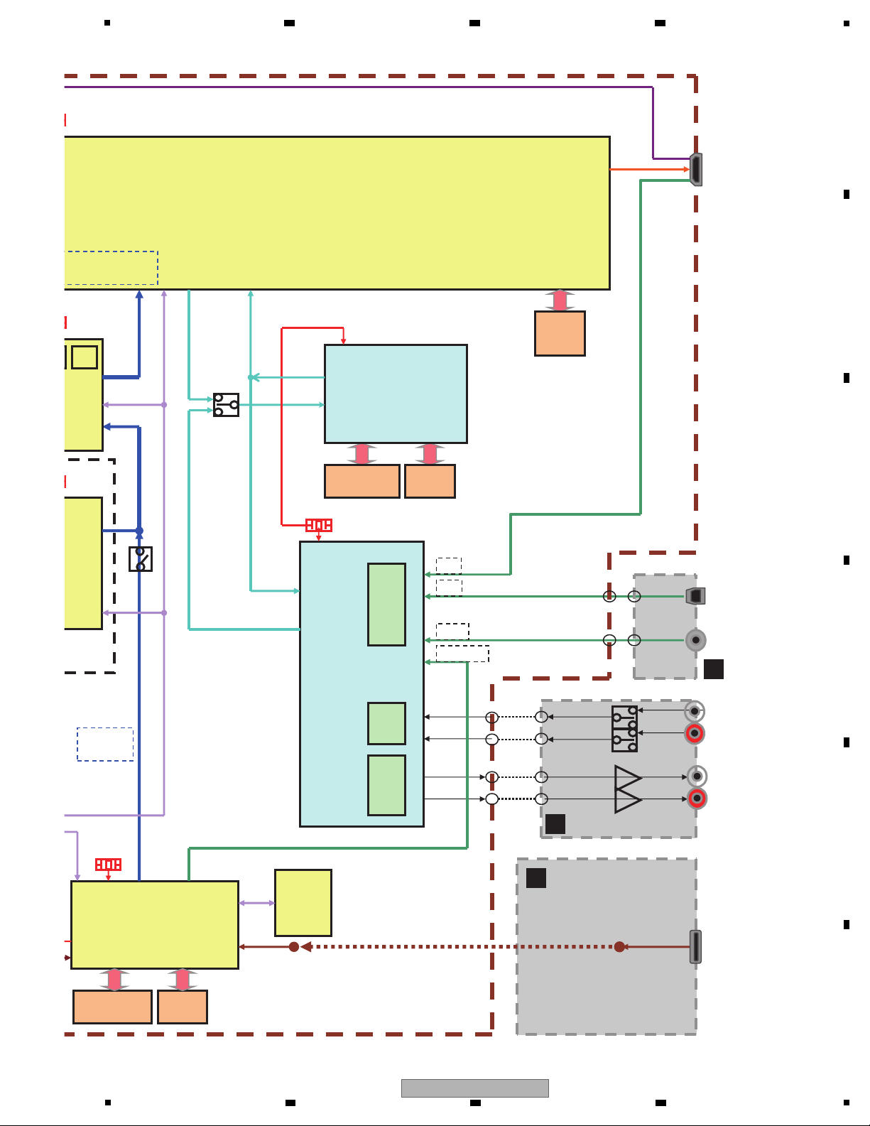
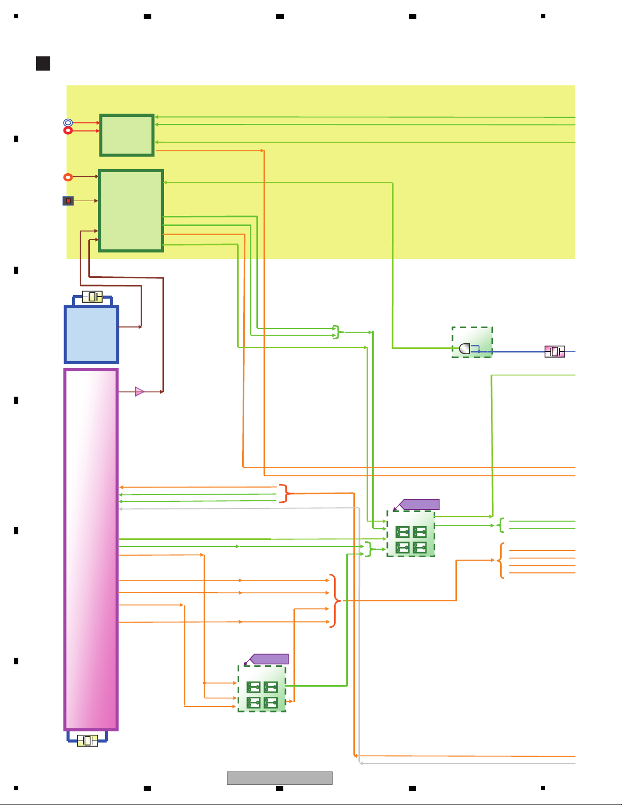
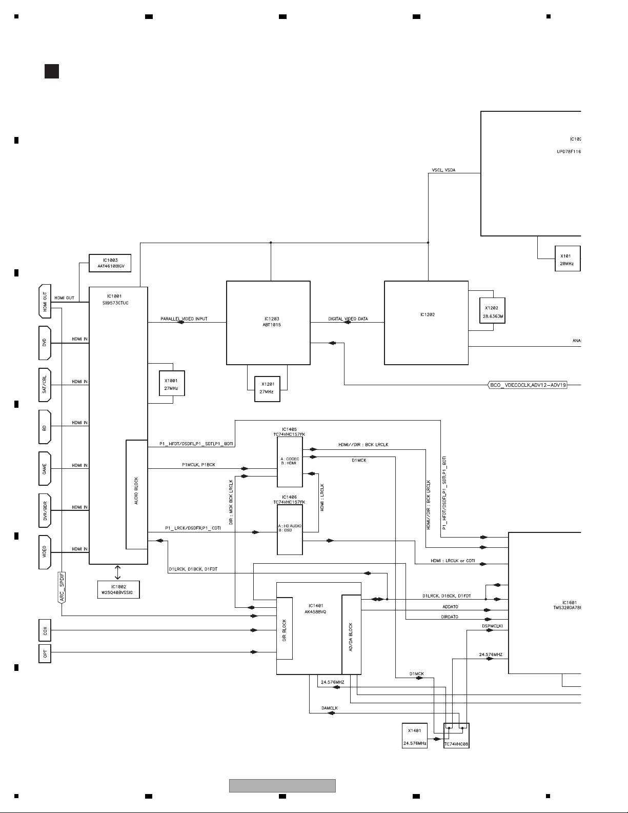
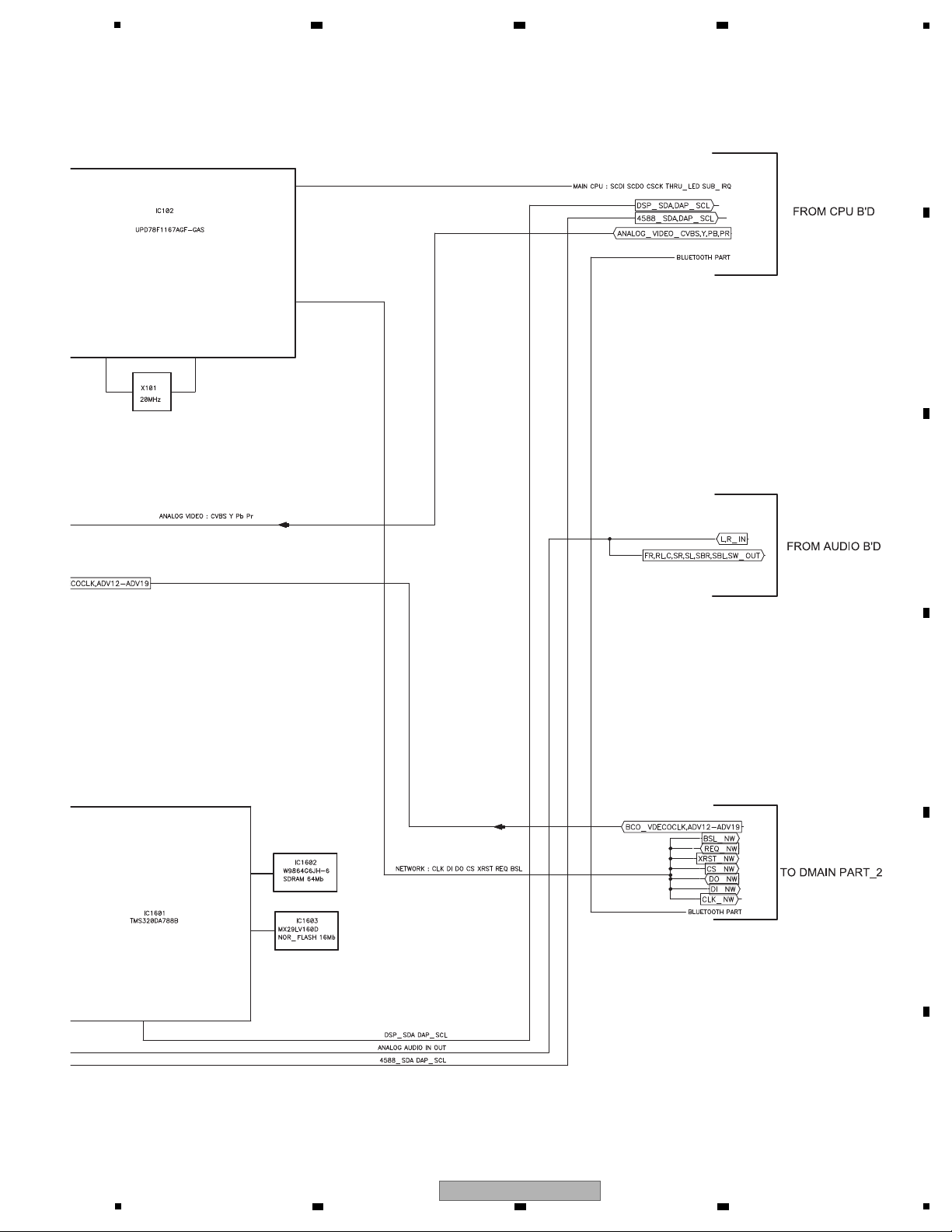
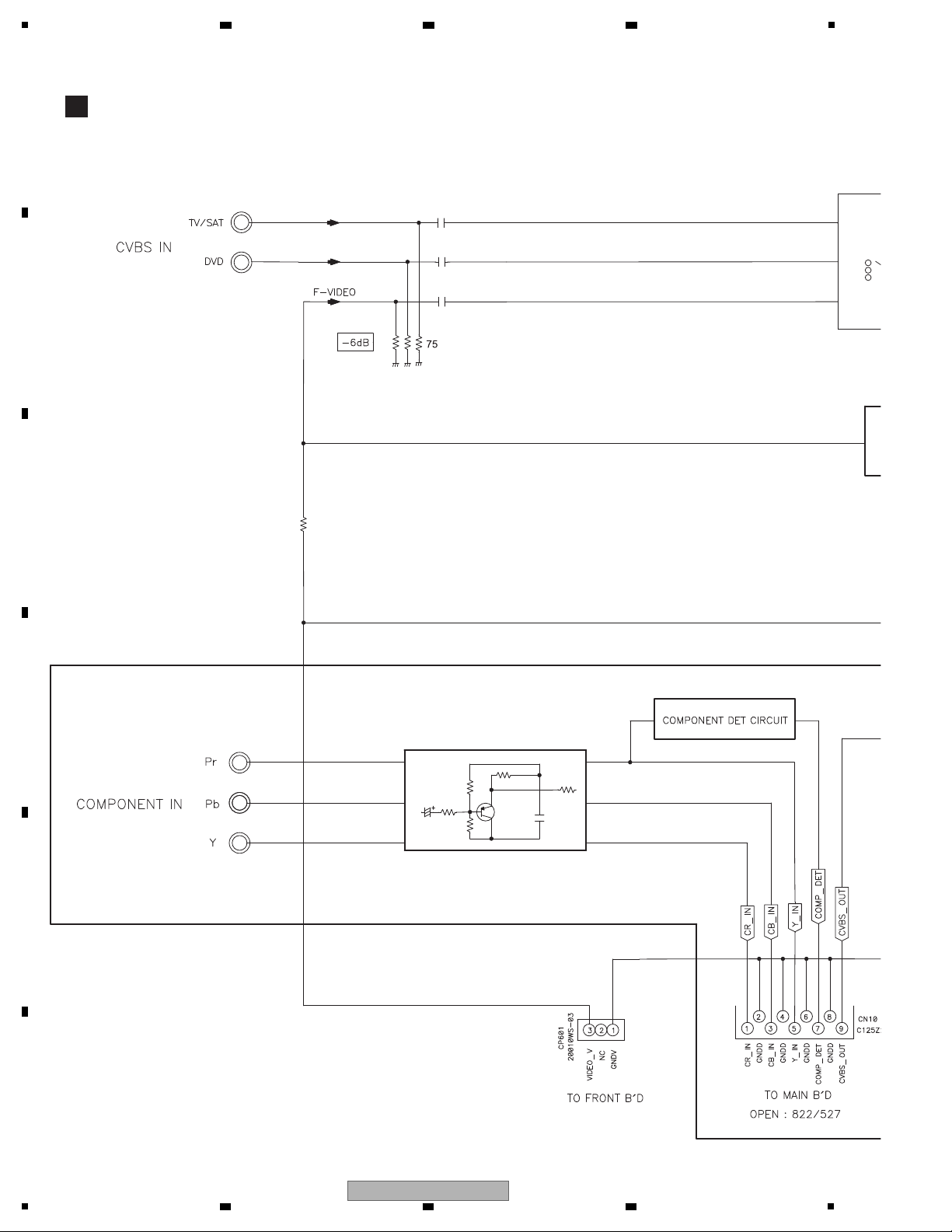
4.4 D-MAIN BLOCK DIAGRAM
A
2 3 4
B
C
D
E
F
18
VSX-1022-K
1
2 3 4
IC 1001
HDMI Port Processor
"SiI9573CTUC"
o
LER
IC 1401
CODEC
"AK4588VQ"
24.576MHz
6MHz
iPod/ USB
HDMI O UT
IC 1601
DSP
" TMS320DA788"
SC
ADC
DAC
OPTICAL IN
COAXIAL IN
IC 9206
Apple
"MF1341
S2164"
ARC
OPT
COAX
NETWORK
SDRAM
64Mb
NOR FLASH
16Mb
AUDIO IN
AUDIO OUT
IC 9204
NETWORK
" DM860A"
NAND
24MHz
SDRAM
256Mb
Only
Serial
FLASH
DIR
CEC
P
F-USB ASSY
A
AUDIO ASSY
L
OPTCO ASSY
5
6 7 8
A
B
C
D
E
F
VSX-1022-K
5
6 7 8
19
1
DIR
COAX 1
OPT 1
ADC
XTI
MC KO 1
BCK2
LRCK2
SDTO 2
DAUX
27.0MHz
I2S DT(multi -ch)
SOURCE - I2S
24MHz
NMP
Bco
DM860
BCK
LRCK
FD/DSDFL
CD/DSDFR
SD
BD
HDMI
Port
Process
or
SII9573
AK4588
AMCLK
BCK
LRCK/DSDF
FD/DSDFL
SD
CD
BD
SEL (VHC157)
IC1405
HDMI_SE
SD
CD/DSDFR
BD
AND(VHC08)
IC1402
24.576MHz
I2S- DATA
I2S- BCK
I2S- LRCK
NETSPDIF
SEL (VHC157)
IC1406
FD/DSDFL
LRCK
LRCK
DSDFR
CD
DSD_SEL
ADDATO
DIRDATO
ARCSPDI
RX4
RX1
RX3
RX2
MSPDIF
DIRMCKI
D
D-MAIN ASSY
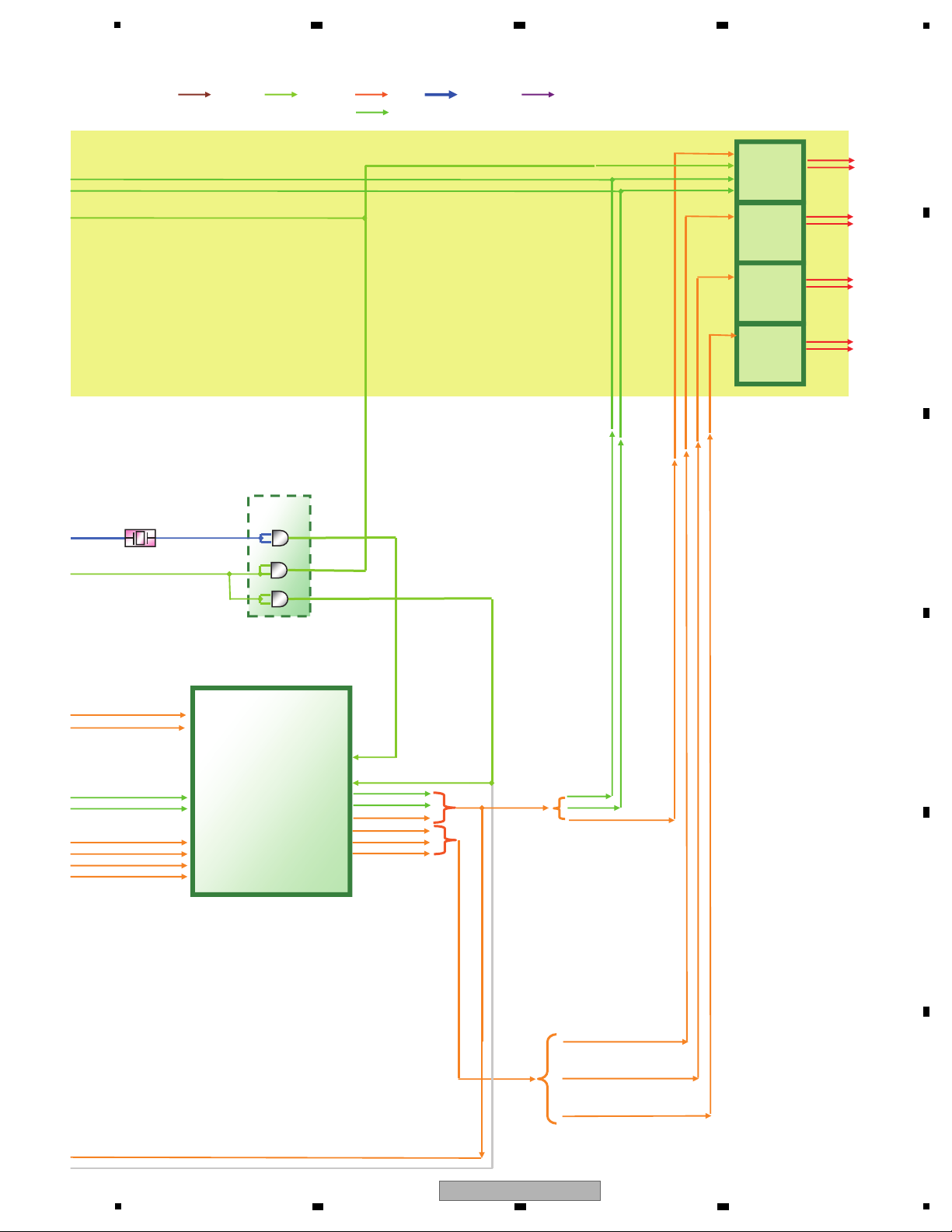
4.5 D-AUDIO BLOCK DIAGRAM
A
2 3 4
B
C
D
E
F
20
1
2 3 4
VSX-1022-K
5
SPDIF AMCLK I2S
I2S- SURR
I2S- C/LFE
I2S- SRB/HEIGHT
SYSCLK FLG
DAC
FL/FR
DAC
C/LFE
DAC
SL/ SR
DAC
SBL/ SBR
I2S- L/R
I2S- C/LFE
I2S- SURR
I2S- SRB/HEIGHT
I2S- BCK
I2S- LRCK
I2S- L/R
I2S- BCK
I2S- LRCK
BCK
LRCK
FD/DSDFL
CD/DSDFR
SD
BD
DSP
DA788
AXR0[9]
AXR0[10]
ACLKR0
AFSR0
AXR0[12]
AXR0[13]
XMCK
AHCLKX0
ACLKX0
AFSX0
AXR0[0]D1FDT
AXR0[1]D1CDT
AXR0[2]D1SDT
AXR0[3]D1BWDT
AXR1[10]D1HWDT
AXR1[11]D1DMDT
DAMCLK
AND(VHC08)
IC1402
24.576MHz
I2S BCK,LRCK
DSPMCLK
ADDATO
DIRDATO
XMCK
6 7 8
A
B
C
D
E
VSX-1022-K
5
6 7 8
F
21
1
D
D-MAIN ASSY
ADV7181CBSTZ
2 3 4
4.6 D-MAIN BLOCK DIAGRAM (1/2)
A
B
C
D
E
F
22
1
2 3 4
VSX-1022-K
5
6 7 8
A
B
C
D
E
F
VSX-1022-K
5
6 7 8
23
1
D
D-MAIN ASSY
IC9204
DM860A
2 3 4
4.7 D-MAIN BLOCK DIAGRAM (2/2)
A
B
C
D
E
F
24
1
2 3 4
VSX-1022-K
IC9204
DM860A
UPD78F1167AGF
5
6 7 8
A
B
C
D
E
F
VSX-1022-K
5
6 7 8
25
1
E
CPU ASSY
4.8 CPU BLOCK DIAGRAM
A
B
2 3 4
C
D
E
F
26
1
2 3 4
VSX-1022-K
5
6 7 8
A
B
C
D
E
F
VSX-1022-K
5
6 7 8
27
1
F
VIDEO ASSY
4.9 VIDEO BLOCK DIAGRAM
A
B
2 3 4
C
D
E
F
28
1
2 3 4
VSX-1022-K
5
6 7 8
A
B
C
D
E
F
VSX-1022-K
5
6 7 8
29
1
C
MAIN ASSY
W
STBY ASSY
2 3 4
4.10 POWER SUPPLY BLOCK DIAGRAM
A
B
C
D
E
F
30
1
2 3 4
VSX-1022-K

5
6 7 8
A
B
C
D
E
F
VSX-1022-K
5
6 7 8
31

1
Step 0: Preliminary confirmation
CN101, CN102, CN1401, CN9202, CN9501
To Step 1
Are the connectors
securely inserted?
Step 1: Fixed board
Confirm the following items before checking
To Step 2
Tighten screws securely.
Do screws of back chassis
securely tighten?
Ye s
Ye s
B to B connector, wire
Ye s
No
Insert the connectors
completely.
No
Step 2: Power supply
CN9501 (pins 1, 2)
IC9501 (pin 3)
Is the voltage 12 V?
Check the wire between D-MAIN
and MAIN Assemblies.
Is the voltage 3.3 V output?
Ye s
Is the voltage 1.8 V output?
Ye s
IC9503 (pin 2)
OK
No OK
Check the IC9501 and its peripheral
circuits or SUB UCOM (IC102).
Check the IC1601 DSP power pin
(dvdd): 3.3 V
V+3R3_HHH LINE of D-MAIN
Assy is OK.
No
Check the IC1203 Scaler POWER pin
(3.3 V, 1.8 V) and its peripheral circuits
or must be replaced IC1203.
No
Check the IC1202 VDEC POWER pin
(3.3 V, 1.8 V) and its peripheral circuits
or must be replaced IC1203.
No
Check the MAIN Assy.
OK
Replace the D-MAIN Assy.
12 V input
(to chassis)
Note 1:
IC1202 - using the model VSX-1022/42/827
[1] DSP TROUBLESHOOTING
TROUBLESHOOTING FOR ALL DESTINATION
5. DIAGNOSIS
5.1 TROUBLESHOOTING
A
B
2 3 4
C
D
E
F
32
1
2 3 4
VSX-1022-K

Ye s
Step 3: Power supply
IC9502 (pin 3)
Is the voltage of 1.2 V
output?
No
OK
Replace the D-MAIN Assy.
Check the IC9502 and its peripheral
circuits or SUB UCOM (IC102).
OK
V+1R2_HHH LINE of D-MAIN
Assy is OK.
Check the IC1601 DSP power pin
(cvdd): 1.2 V
Ye s
Step 4: Power supply
IC9506 (pin 4)
Is the voltage of 5 V
output?
No
OK
Replace the D-MAIN Assy.
Check the IC9506 and its peripheral
circuits or SUB UCOM (IC102).
OK
V+5_HD LINE of D-MAIN Assy
is OK.
Check the IC1401 power pin
(dvdd & avdd): dvdd: 5 V, avdd: 5 V
Ye s
Step 5: Power supply
IC9504 (pin 3)
IC9505 (pin 1)
Is the voltage of 3.3 V
output?
Is the voltage of 1.2 V
output?
Ye s
No
OK
Replace the D-MAIN Assy.
Check the IC9504 and its peripheral
circuits or SUB UCOM (IC102).
No
Check the IC9204 NW POWER pin
(3.3 V, 1.2 V) and its peripheral
circuits or must be replaced IC9505.
OK
V+3R3_NW LINE of D-MAIN Assy
is OK.
Check the IC9204 NW power pin
(vdd33, vdd12): 3.3 V, 1.2 V
5
6 7 8
A
B
C
D
E
F
VSX-1022-K
5
6 7 8
33

A
Ye s
Step 7: DIR
CN1402 (pins 5, 8)
IC1401 (pin 67)
IC1401 (pin 61)
Can observe the
digital signal?
Check the wire between D-MAIN
and OPTCO Assemblies.
Check that the S/PDIF signal is input.
Check that changes by pulling out and inserting the digital input lines.
No
Ye s
Can observe the
digital signal?
Check the path to pins 10 to 13 of
IC1403 or replace IC1403.
Can observe the
digital signal?
Ye s
Ye s
No
Check the path to pin 8 of CN1402
or replace IC1403.
No
OPT
5: COAX
8: OPT
COAX
(0 V ↔ 3.3 V)
(0 V ↔ 3.3 V)
(0 V ↔ 3.3 V)
IC1401 (pin 59)
Can observe the
digital signal?
Ye s
Check the path to pins 1 to 4 of IC1403
or replace IC2009.
No
ARC
(0 V ↔ 3.3 V)
IC1401 (pin 63)
Can observe the
digital signal?
Check the path to pins U3 of IC9204
or replace the D-MAIN Assy.
No
Network/USB/iPod
SPDIF INPUT line is OK.
Ye s
Step 6: X'tal
IC1401 (pin 7)
IC1601 (pin 17)
Is there a 24.576 MHz
output?
Check the IC1401, IC1402 and its peripheral
circuits or replace the D-MAIN Assy.
No
Ye s
Is there a 24.576 MHz
input?
Check the IC1601 and its peripheral
circuits or replace the D-MAIN Assy.
No
DIRMCKI
XMCK
To Step 7
B
1
2 3 4
C
D
E
F
34
1
2 3 4
VSX-1022-K

5
Replace IC1405.
IC1401 (pin 14)
Ye s
Ye s
IC1405 (pin 4)
DIR output is OK.
Is there a DATA output?
Is there a master clock
24.576 MHz output?
Ye s
Is the voltage of IC1405
pin 1 0 V?
DIRDATO (DATA)
D1MCLK (MASTER CLOCK)
*IC1405 pin 1
0 V: DIR
3.3 V: HDMI
SWITCH
(0 V ↔ 3.3 V)
(0 V ↔ 3.3 V)
Check the IC1401 and its peripheral
circuits of IC1401.
No
Check the path between pin1 of
IC1405 and pin 20 of CN102.
No
Replace IC1401.
OK
No
Ye s
Step 8: ADC
CN1401 (pins 17, 19)
IC1401 (pin 17)
IC1401 (pin 18)
Is there a analog audio
signal?
Is there a analog
audio signal of BRG-1 Assy
CP403 pins 17, 19?
Check that the ANALOG input to DSP mode.
Ye s
No
No
Replace CP2003 wafer of BRG-1 Assy,
or reconnect BRG-1 Assy.
Is there a data
output?
Ye s
ANALOG AUDIO input
ADDATO (ADC AUDIO OUT)
D1BCK
(0 V ↔ 3.3 V)
Check the AUDIO Assy.
No
Is there a bit clock
3.072 MHz input?
Ye s
(0 V ↔ 3.3 V)
No
IC1401 (pin 19)
D1LRCK
Is there a LR clock
48 kHz input?
Ye s
(0 V ↔ 3.3 V)
No
To Step 9
Check the path between IC1601 and data & address lines. SDRAM
(IC1602), FLASH ROM (IC1603), replace the D-MAIN Assy.
Ye s
No
Check the IC1401 and its peripheral
circuits of IC1401.
No
Check the IC1405 and its peripheral
circuits of IC1405.
OK
Check the pin 11 of CN102,
is the voltage 3.3 V?
No
No
Replace IC1401, IC1405.
Check the CPU Assy.
OK
Check the CPU Assy.
OK
IC1401 (pin 10)
IC1401 (pins 15, 16)
Ye s
Is there a master clock
24.576 MHz output?
Is the voltage of PDN IC1401
pin 31 3.3 V?
Is there a LR clock or BIT
clock output?
DIRMCKO (master clock)
15: DIRBCK (bit clock)
16: DIRLRCK (LR CLOCK)
(0 V ↔ 3.3 V)
(0 V ↔ 3.3 V)
Check that the data and clock signals are output.
6 7 8
A
B
C
5
6 7 8
VSX-1022-K
D
E
F
35
1
Ye s
Step 9: DSP mode audio output
IC1401 (pin 18)
IC1401 (pin 19)
Is there a bit clock input?
Digital output of each CH when inputting the digital signal with audio.
Is there a LR clock
output?
Is there a data input?
Is there a data input?
Is there a data input?
Is there a data input?
Ye s
IC1401 (pin 28)
IC1401 (pin 27)
Ye s
IC1401 (pin 26)
Ye s
IC1401 (pin 25)
Ye s
Ye s
D1BCK (BIT CLOCK)
D1LRCK (LR CLOCK)
front L/R data
surround L/R data
CENTER/LFE data
surround back L/R data
or front hight L/R data
(0 V ↔ 3.3 V)
(0 V ↔ 3.3 V)
(0 V ↔ 3.3 V)
(0 V ↔ 3.3 V)
(0 V ↔ 3.3 V)
(0 V ↔ 3.3 V)
To Step 10
No
No
No
No
No
No
Check the path between IC1601 and data & address lines. SDRAM
(IC1602), FLASH ROM (IC1603), replace the D-MAIN Assy.
A
2 3 4
B
C
D
E
F
36
VSX-1022-K
1
2 3 4

5
Ye s
Step 10: CODEC output (ANALOG AUDIO OUT)
IC1401 (pin 49)
IC1401 (pin 47)
Is there a audio signal
output?
Analog output of each CH when inputting the digital signal with audio.
Analog output of each CH when inputting
the digital signal (-∞ dB(no signal)).
Ye s
Is there a audio signal
output?
front R out
front L out
IC1401 (pin 45)
Ye s
Is there a audio signal
output?
surround R out
IC1401 (pin 43)
Ye s
Is there a audio signal
output?
surround L out
IC1401 (pin 43)
surround L out
IC1401 (pin 41)
Ye s
Is there a audio signal
output?
center out
Ye s
IC1401 (pin 41)
center out
IC1401 (pin 39)
Ye s
Is there a audio signal
output?
LFE out
Ye s
Ye s
IC1401 (pin 39)
LFE out
IC1401 (pin 49)
Ye s
Is the output 2.5 V fixing?
front R out
IC1401 (pin 47)
Ye s
Is the output 2.5 V fixing?
front L out
IC1401 (pin 45)
Ye s
Is the output 2.5 V fixing?
Is the output 2.5 V fixing?
Is the output 2.5 V fixing?
Is the output 2.5 V fixing?
surround R out
End
No
No
No
No
No
No
No
No
No
No
No
No
Replace IC1401.
6 7 8
A
B
C
D
VSX-1022-K
5
6 7 8
E
F
37

1
Cause for noncomplection of HDMI authentication between the source equipment and this unit.
(the HDMI indicator is unlit or flasher)
Causes for no display or sound from the monitor
[2] HDMI TROUBLESHOOTING
Replace the HDMI cable.
NG
OK
Replace the HDMI cable.
Connect the source equipment
(player) to the Sink equipment
(monitor) directly.
OK
Repare the Receiver.
NG
Replace the Player.
OK
Repare the Player.
NG
Replace the Monitor.
OK
Repare the Monitor.
HDMI Troubleshooting
HDMI Simple Diagnosis
Step 0: Preliminary confirmation
Confirm the following items before checking
To Step 1
Do screws of back chassis
securely tighten?
To Step 2
Tighten screws securely.
Ye s
No
Step 1: Connect the HDMI equipment
Source equipment:
Connect a DVD player to DVD or SAT/CBL or BD or GAME or
DVR/BDR or VIDEO.
Sink equipment:
Connect a TV to HDMI OUT
Turn on the power of the receiver and equipments which was
connected with HDMI.
Function switch
(DVD or SAT/CBL or BD or GAME or DVR/BDR or VIDEO)
POWER ON
A
2 3 4
B
C
D
E
F
38
1
2 3 4
VSX-1022-K
Step 2: Power supply
IC103 (pin 4)
Is the voltage 3.3 V
output?
Is the voltage pin 5 of IC103
above 6 V?
Ye s
Ye s
No
Check the IC9506 and its peripheral
circuits or SUB UCOM (IC102).
Is the voltage 12 V?
No
Diagonose the MAIN Assy.
No
Diagonose the CPU Assy.
No
Replace the D-MAIN Assy.
V+3R3_SB
CN9501 (pins 1, 2)
HDMI+12V
Ye s
Is the voltage 5 V?
No
Check the IC9501 and its peripheral
circuits or SUB UCOM (IC102).
No
Replace the D-MAIN Assy.
No
IC9506 (pin 4)
V+5_HD
Ye s
Is the voltage 3.3 V?
IC9501 (pin 3)
V+3R3_HHH
Check the IC9503 and its peripheral
circuits or SUB UCOM (IC102).
No
Replace the D-MAIN Assy.
No
Ye s
Is the voltage 1.8 V?
IC9503 (pin 2)
V+1R8_HHH
Check the IC9502 and its peripheral
circuits or SUB UCOM (IC102).
No
Replace the D-MAIN Assy.
No
Ye s
Is the voltage 1.2 V?
IC9502 (pin 3)
V+1R2_HHH
To Step 3
5
6 7 8
A
B
C
D
5
VSX-1022-K
6 7 8
E
F
39

1
Check the parts and patterns
in the path pin 3 of IC102.
Check the parts and patterns in the
path pins 1, 2 of IC102. If IC1001 is
failure, replace the D-MAIN Assy.
Check the parts and patterns in
the path pins 1, 2 of IC102.
If IC1203 is failure, replace IC1203.
Check the parts and patterns in
the path pin 7 of IC102.
Check the parts and patterns in
the path pin 8 of IC102.
No
IC1001 (pin 69)
Is the voltage 0 to 3.3 V?
No
No
Does a signal
output in constant period?
(0 to 3.3 V)
Is there a data output?
(0 to 3.3 V)
XHDPP_RST
66: VSCL
67: VSDA
IC1001 (pins 66, 67)
Ye s
XABT_RST
IC1203 (pin 53)
No
Is there a data
input and output?
(0 to 3.3 V)
XADV_RST
IC1202 (pin 51)
Ye s
No
Check the parts and patterns in
the path pins 1, 2 of IC102.
If IC1203 is failure, replace IC1203.
Check the line and IC1202.
If IC1202 is failure, replace IC1202.
IC1202 (pin 36 (CVBS), 47 (CR),
48 (CB), 49 (Y), 50 (SOY))
No
Does a signal
output in constant period?
(0 to 3.3 V)
62: VSCL
61: VSDA
54: VSCL
53: VSDA
Note1:
IC1202 - using the model VSX-1022/42/827
IC1203 (pins 62, 61)
Ye s
Step 3: Diagnosis
Each data lines confirmation checks it after standby off/on.
Ye s
Does a signal
output in constant period?
(0 to 3.3 V)
IC1202 (pins 54, 53)
Ye s
Ye s
To Step 4
Check the X1001 and its
peripheral circuits or replace
the D-MAIN Assy.
Check the X1202 and its
peripheral circuits or replace
IC1202.
No
No
Ye s
IC1001 (pins 113, 114)
Is there a 27 MHz
input/output?
Is there a 28.63636 MHz
input/output?
IC1202 (pins 21, 22)
Ye s
Ye s
Yes (3.3 V)
Ye s
Step 4: X'TAL
Turn the power off and insert
the wire securely.
No
COMP_DET
CN101
Are the connectors
securely inserted?
Does a signal output
in constant period?
(WAVE)
Check the line and IC102.
Check the VIDEO Assy.
No
No
IC102 (pin 12)
Does a signal
output high (3.3 V)?
When inserting
Component Y signal.
SIGNAL INPUT
IC1202 (pins 36, 47, 48, 49, 50)
Step 5: ANALOG UP (VSX-1022/42/827 only)
Ye s
To Step 6
To Step 5
Check the X1201 and its
peripheral circuits or replace
IC1203.
Check the IC1201 and its
peripheral circuits or replace
IC1201.
No
Ye s
No
Is there a 27 MHz
input?
IC2003 (pin 7)
IC1201 (pins 1, 2, 6)
Ye s
Is there a 27 MHz
input?
A
A
TMDS OUTPUT
Check the IC1001. If IC1001 is
failure, replace the D-MAIN Assy.
No
Ye s
IC1001
(pins 152,153,154,155,156,157,158,159)
Are there signals
(approx. 0.5 Vp-p)
IN all lines?
Step 6: TMDS
End
A
2 3 4
B
C
D
E
F
40
1
2 3 4
VSX-1022-K

5
Ye s
Step 7: HDMI AUDIO
IC1001 (pin 125)
Is there a 24.576 MHz
output?
Is there a 12.28 MHz
output?
*play is Dolby thru HD @ dts master audio source
Ye s
Ye s
Ye s
Ye s
Ye s
Ye s
Ye s
HDMI audio MASTER clock
output
IC1001 (pin 122)
HDMI audio BIT clock output
(0 V ↔ 3.3 V)
(0 V ↔ 3.3 V)
Is there a 192 kHz
output?
IC1001 (pin 121)
HDMI audio LR clock output
(0 V ↔ 3.3 V)
Can observe the
digital signal?
IC1001 (pin 124)
HDMI audio front L/R OUT
(0 V ↔ 3.3 V)
Can observe the
digital signal?
IC1001 (pin 127)
HDMI audio surround L/R OUT
(0 V ↔ 3.3 V)
Can observe the
digital signal?
IC1001 (pin 126)
HDMI audio center/sw OUT
(0 V ↔ 3.3 V)
Can observe the
digital signal?
IC1001 (pin 128)
HDMI audio surroundback OUT
HDMI audio front hight OUT
(0 V ↔ 3.3 V)
Can observe the
digital signal?
IC2016 (pins 134,135,137,138)
HDMI AUDIO is OK
(0 V ↔ 3.3 V)
No
No
No
No
No
No
No
No
Check the VDD_PLL and GND
lines. Replace the D-MAIN Assy.
Check the switching IC.
IC1405, IC1406.
6 7 8
A
B
C
D
5
VSX-1022-K
6 7 8
E
F
41

1
[3] iPod TROUBLESHOOTING
Step 1: Diagnosis
Step 0: iPod/USB Power supply
CN9202 (pins 2, 3)
Are there any digital data
signals?
Check the wire between D-MAIN
Assy and F-USB Assemblies.
No
Check the F-USB Assy.
Check the USB data line.
No
No
No
Check the path between
IC9024 (pin J2).
No
To Step 1
To Step 2
CN9201 (pin 6)
CN9201 (pin 4)
Is pin 6 (USBDDCERR)
of CN9201 low?
Ye s
Ye s
Ye s
Ye s
Ye s
Ye s
Replace the D-MAIN Assy.
No
Check the F-USB Assy.
Is pin 4 (XUSBERR)
of CN9201 low?
Ye s
No
CN9201 (pin 5)
Check the path between
IC9204 (pin K2).
Is pin 5 (USBPOW)
of CN9201 high?
Ye s
No
When SCL and SDA are normal operation = high (3.3 V)
Connect iPod, and communicate it about 10 seconds later (authentication starts).
And communicate it about 60 seconds later (authentication is complete).
Step 2: Operation of iPod (Authentication process)
IC9204 (pins A1, B1)
IC9206 (pins 12, 13)
USB data D+, D-
SCL_AP, SDA_AP
(I2C between IC9204 and IC9206)
Do D+ and D-
communicate?
Do SCL and SDA
communicate?
Does XAPRST (pin 4)
reset it?
High after the reset.
Operation of IC9206 is OK.
To Step 3.
Refer to Step 7 of
"[1] DSP TROUBLESHOOTING."
Replace the D-MAIN Assy.
Step 3: Audio out check
IC9204 (pin U3)
Is there a signal?
No
NETSPDIF
A
2 3 4
B
C
D
E
F
42
VSX-1022-K
1
2 3 4

5
Step 0: Preliminary confirmation
Confirm the following items before checking
To Step 1
Do screws of PLATE_SCREW
securely tighten ?
Ye s
To Step 2
To Step 3
Ye s
[4] BT (Bluetooth) TROUBLESHOOTING
Tighten screws securely.
No
Check the BT Assy.
Step 1: BT_DET
CN101 (pin 11)
Is the voltage 0 V?
Check the pattern in the path
and BT, BTCNT, MAIN and
CPU Assemblies.
No
Check the pattern in the path.
Check the BTCNT Assy.
Check the MAIN Assy.
Ye s
Step 2: Diagnosis
CN101 (pin 12)
CN101 (pin 13)
Is pin 12 (BTOL) of CN101
low?
No
Check the path between
IC9204 (pin T13).
Ye s
Is pin 13 (BTPOW) of CN101
high?
No
CN101 (pins 14, 15)
BTRX2 and BTTX should be
high during operation.
Check the pattern in the path of
BT Assy and CPU Assy.
Ye s
Do BTRX2 and
BTTX communication with
IC9204?
No
Ye s
OK
Check the AUDIO Assy.
OK
Step 3: Audio out check
CP603 (pins 1, 3)
Is there a audio signal?
No
1: BT_R
3: BT_L
14: BTRX2
15: BTTX
XBT_DET
6 7 8
A
B
C
D
E
F
VSX-1022-K
5
6 7 8
43

1
Functional Name
Adapter port overcurrent detection
Outline
When the BT adapter is inserted in Adapter port, turn off the power of the Adapter port forcibly when it detects an
overcurrent. And display ERROR state in FL.
Explain Operation Detail
For detection method
• Confirm a detection port at intervals of 20 msec to 50 msec (*2), and judge it as an overcurrent when you detected an error
consecutively three times.
*2 It is assumed that it is fixed value of the 20 msec to 50 msec degree.
*1 Return the "ADP ERR" display to the normal display if you change it into other FUNCTION only in the
APAPTER PORT FUNCTION.
Also display "ADP ERR" if the ADAPTER PORT FUNCTION is ERROR state.
Basic Operation
Front Key Sequence
Change
Character Display Time (sec.)
Icon Display
(FL)
LED Display
A
*1
When the overcurrent is
detected
The display continues until the
power is turned off.
Check it after turning the power once
off then back on again, and it becomes
the normal operation if normal.
D P E R R
12 12345678
Functional Name
iPod ERROR MESSAGE
Outline
Error message is displayed at abnormality time.
Basic Operation
Front Key Sequence Change Time (sec) FL Display
Over Current Error
I/U ERR
2 3 4
5.2 ADAPTER ERROR MESSAGE
A
B
C
D
5.3 USB/iPod ERROR MESSAGE
E
F
44
1
2 3 4
VSX-1022-K

5
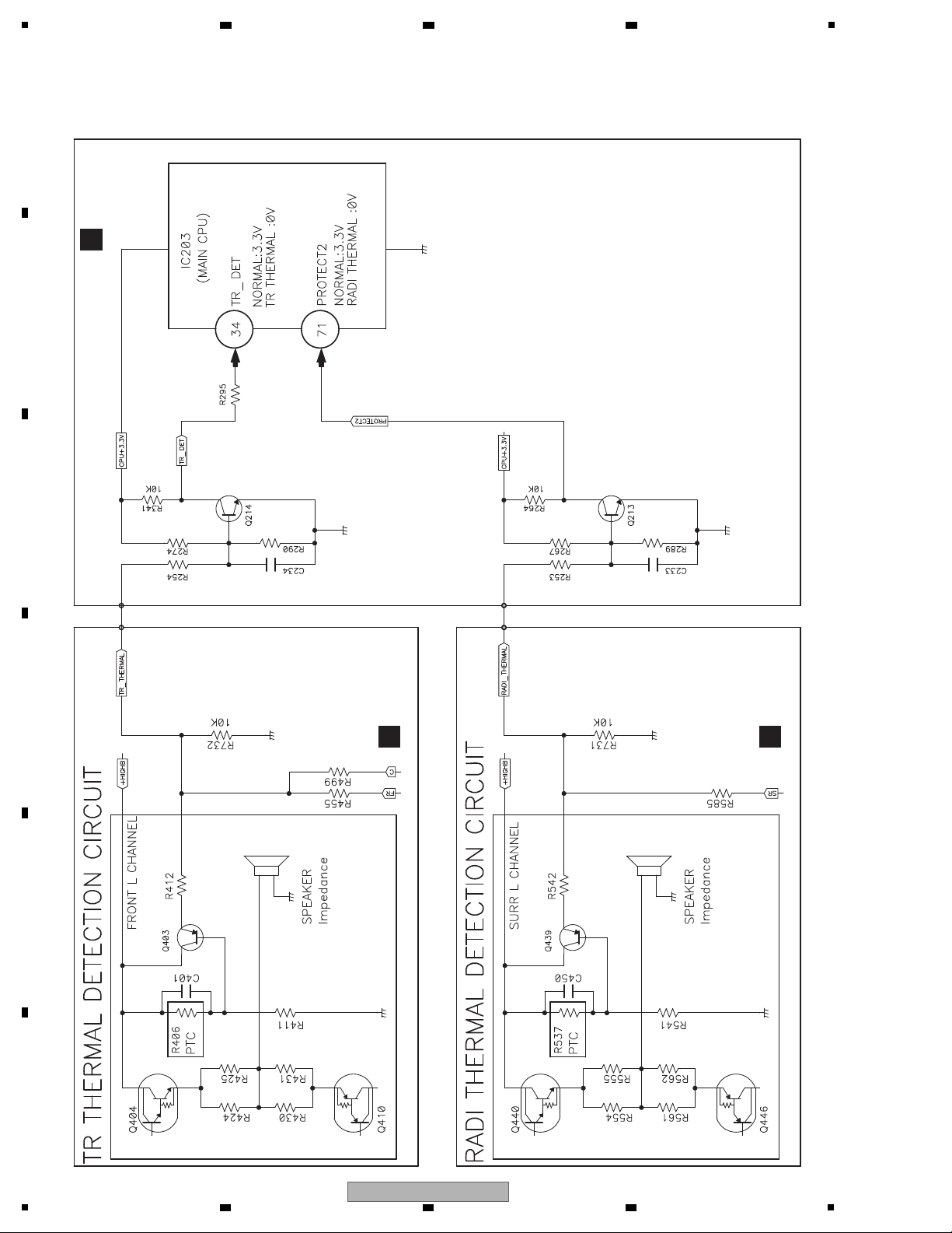
[1] Overload and DC Protection Circuit
E
CPU ASSY
B
AMP7/AMP5 ASSY
B
AMP7/AMP5 ASSY
C
MAIN ASSY
5.4 DETECTION CIRCUIT
6 7 8
A
B
C
D
E
F
VSX-1022-K
5
6 7 8
45
1
[2] TEMP Protection Circuit
E
CPU ASSY
B
AMP7/
AMP5 ASSY
B
AMP7/
AMP5 ASSY
A
B
2 3 4
C
D
E
F
46
1
2 3 4
VSX-1022-K

5
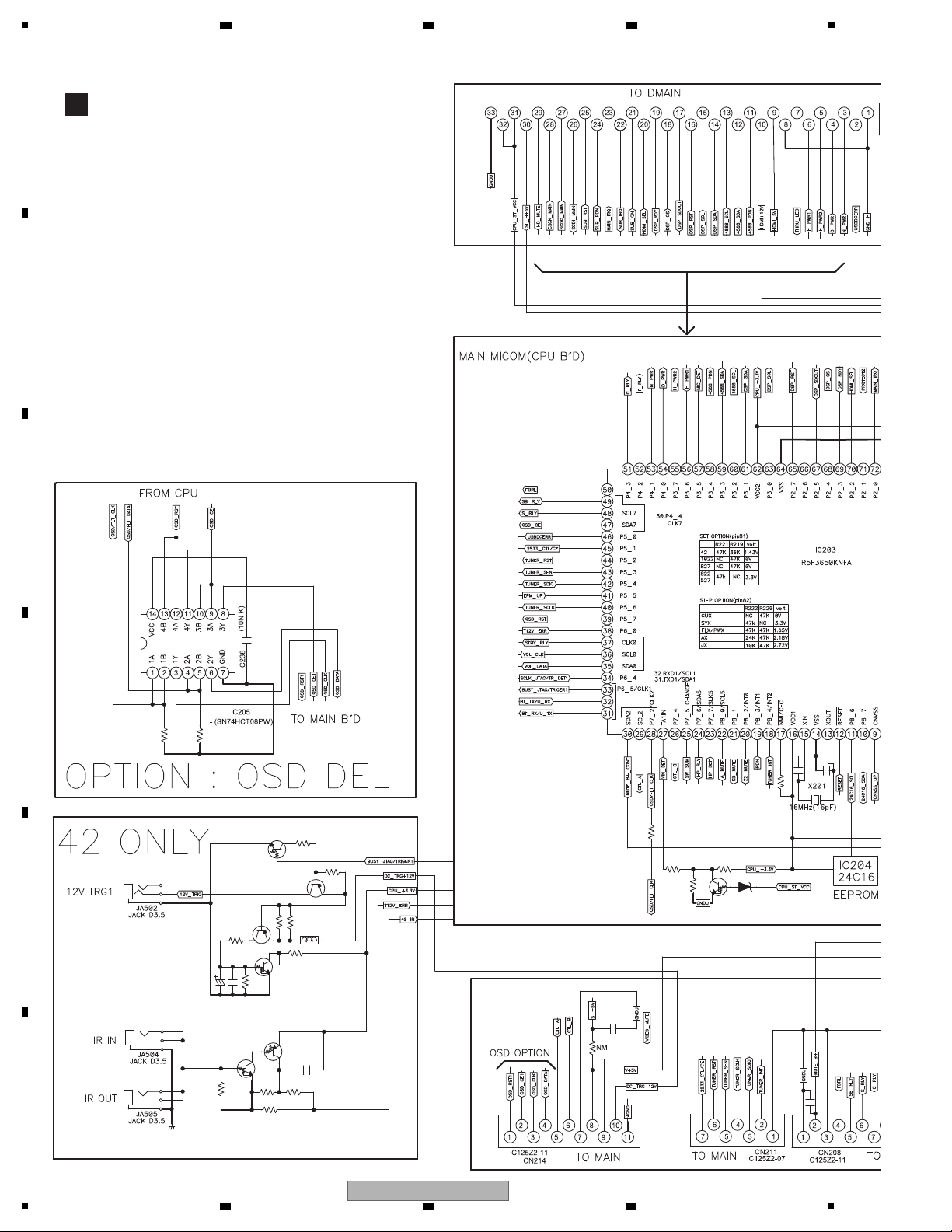
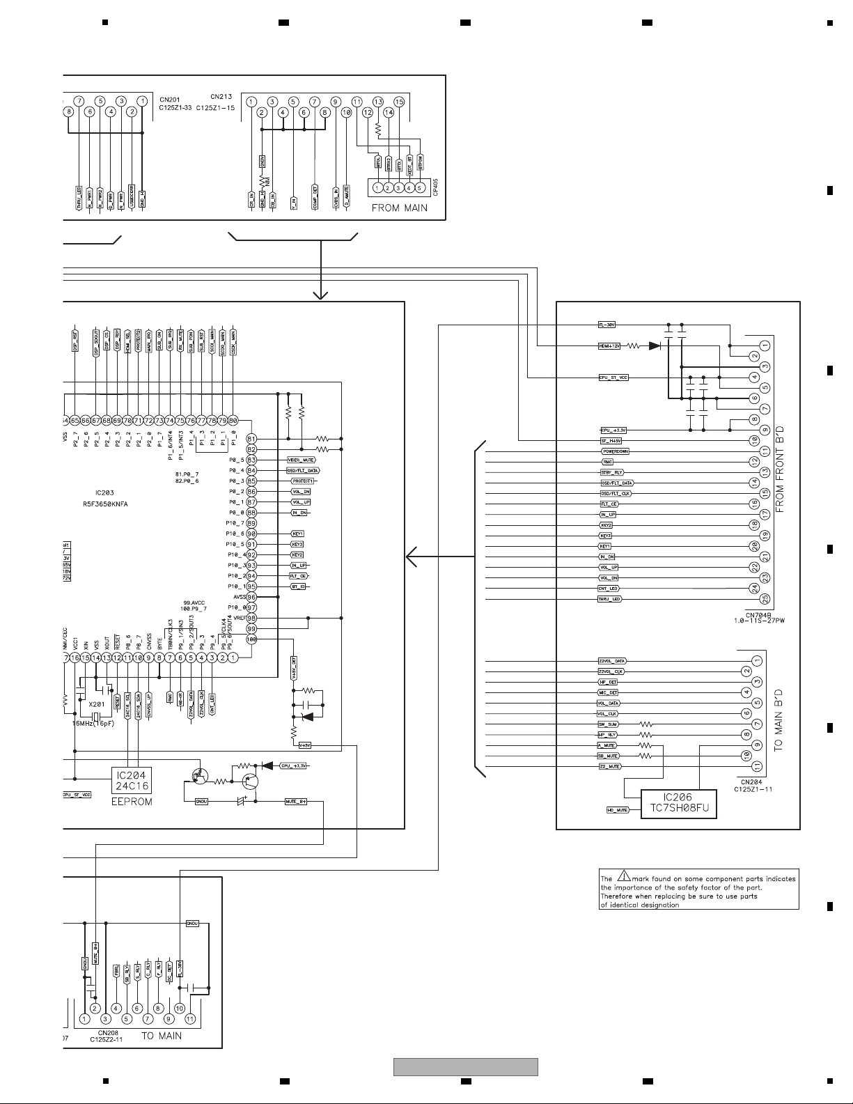
(R5F3650KNFA)(CPU ASSY: IC203)
MAIN Microcomputer
• Pin Function
No. Symbol I/O Description
1 P9_6/SOUT4 O Not used
2 P9_5/CLK4 O Not used
3CNT_LED O Power LED control signal
4Z2VOL_CLK O CLK signal output for BD3812F (I2C)
5Z2VOL_DATA O Data signal output for BD3812F (I2C)
6 40-IR I Infra_red signal input
7 RMC I Remote control signal input pin
8 GNDU I The data bus is 16 bits long when the this pin is held "L" (GND)
9CNVSS_UP I Switches processor mode
10 24C16_SDA I/O Data signal input & output for data backup of MAIN UCOM
11 24C16_SCL O Clock signal output for data backup of MAIN UCOM
12 /RESET I UCOM reset signal input pin (active at L)
13 XOUT O Output for 16 MHz Crystal
14 VSS – Ground
15 XIN I Input for 16 MHz Crystal
16 VCC1 – +3.3 V power supply
17 /NMI I Input pin for the NMI interrupt
18 TUNER_INT I Tuner Interrupt signal input pin
19 PDN I Power down signal input pin
20 Z2_MUTE O Z2 ch. Audio output control pins at Mute Tr (active at L)
21 SB_MUTE O SB ch. Audio output control pins at Mute Tr (active at L)
22 A_MUTE O Audio output control pins at Mute Tr (active at L)
23 HP_DET I Monitoring the input pin headphone connection
24 HP_RLY O Headphone audio output control pins at Mute Tr (active at L)
25 SW_SUM O Output for Sub Woofer SUMMING Control(H:SUMMING)
26 CTL_B O IC control signal B output pin for selecting the video input
27 VIN_DET I Input for st_pwr condition
28 OSD/FLT_CLK O OSD & FL drive Ic output pin of the Data
29 CTL_A O ICcontrol signal A output pin for selecting the video input
30 MUTE_B+_CONT O Power control pin mute B+
31 BT_RX/U_TX O Data signal output from BLUETOOTH Antenna
32 BT_TX/U_RX I Data signal input from BLUETOOTH Antenna
33
BUSY_JTAG/TRIGER1 O Output for JTAG BUSY/TRIGER1_ON/OFF SIGNAL
34 SCLK_JTAG/TR_DET' I CLOCK SIGNAL Input for SCLK_JTAG/TR_DET'
35 VOL_DATA O Data signal output for R2A15219 (I2C)
36 VOL_CLK O CLK signal output for R2A15219 (I2C)
37 STBY_RLY O Output to ST-BY Relay ON/OFF (active at H)
38 T12V_ERR I Input for dc_trg_err condition
39 OSD_RST O OSD IC Reset signal output pin
40 TUNER_SCLK O Clock signal output for Tuner Pack
41 EPM_UP I UPGRADE
42 TUNER_SDIO I/O Data signal input & output for Tuner Pack
43 TUNER_SEN O Output for Tuner Pack Serial Enable Input (active at L)
44 TUNER_RST O Output to reset Tuner Pack (active at L)
45 2533_CTL/CE O Output for NJM2533 control on/off signal
46 USBDCERR O Input for usb_dc_err condition
47 OSD_CE O OSD IC enable signal output pin
48 S_RLY O Tr driven control pins at the Surround speaker output Relay. (active at H)
49 SB_RLY O Tr driven control pins at the Surround Back speaker output Relay. (active at H)
50 FBRL O Tr driven control pins at the F.H /B speaker output Relay. (active at H)
6 7 8
5.5 IC INFORMATION
A
B
C
D
E
F
VSX-1022-K
5
6 7 8
47

1
• Pin Function
No. Symbol I/O Description
51 C_RLY O Tr driven control pins at the Center speaker output Relay.(active at H)
52 F_RLY O Tr driven control pins at the Front speaker output Relay. (active at H)
53 N_PWR O Control pin digital +3.3 V DC/DC IC (on: H)
54 D_PWR O Control pin digital +3.3 V DC/DC IC (on: H)
55 H_PWR2 O Control pin digital +1.2 V DC/DC IC (on: H)
56 H_PWR1 O Control pin HDMI IC +5.0 V REG. IC (on: H)
57 MIC_DET O Monitoring the input pin microphone connection (detection: L)
58 4588_PDN O Output for AK4588 power down
59 4588_SDA O Data signal output for AK4588 (I2C)
60 4588_SCL O Clock signal output for AK4588 (I2C)
61 DSP_SDA O Data signal output for DA787 (DA789) (I2C)
62 VCC2 – +3.3 V power supply
63 DSP_SCL O Clock signal output for DA787 (DA789) (I2C)
64 VSS – Ground
65 DSP_RST O Output to reset DA787(DA788)
66 NC–Not used
67 DSP_SDOUT I Data signal Input from DA787 (DA788)
68 DSP_CS O Output for DA787 (DA788) chip select
69 DSP_RDY I Input for DA787 (DA788) SPI Enable
70 HDMI_SEL O IC signal of the control pins at select HDMI or analog audio
71 PROTECT2 I AMP Assy input signal of the RADIATOR THERMAL pin (L= PROTECTION)
72 MAIN_IRQ O Interrupt Output to SUB UCOM
73 SUB_ON O Output for SUB UCOM Power ON/OFF cotrol pin
74 SUB_IRQ I Interrupt Iuput from SUB UCOM
75 HD_MUTE I Input for HDMI_RX_MUTE condition
76 SUB_PDN O Output for SUB UCOM power down
77 SUB_RST O Output to reset SUB UCOM
78 SCDI_MAIN I
Data signal input from SUB UCOM
79 SCDO_MAIN O Data signal output to SUB UCOM
80 CSCK_MAIN O Clock signal output for SUB UCOM
81 SET OPTION I Input for Set option
82 STEP OPTION I Input for Step (Group) option
83 VIDEO_MUTE O Output for NJM41050 mute cotrol pin
84 OSD/FLT_DATA O OSD & FL drive Ic output pin of the Data
85 PROTECT1 I AMP Assy Protection detection signal input pin (ASO= 0.82 V, DC= 1.39 V)
86 VOL_DN I Data input for VOLUME encoder (VOLUME DOWN is counterclockwise direction)
87 VOL_UP I Data input for VOLUME encoder (VOLUME UP is clockwise direction)
88 IN_DN I Data input for INPUT selector encoder
89 NCINot used
90 KEY1 I Data input for Key1 scan
91 KEY3 I Data input for Key3 scan
92 KEY2 I Data input for Key2scan
93 IN_UP I Data input for INPUT selector encoder
94 FLT_CE O Output for chip enable of SC16315
95 NCONot used
96 GND – Ground
97 NCONot used
98VREF – Reference voltage (Connected to +3.3 V)
99 AVCC – +3.3 V power supply
100 V+5V_DET
I Output to ST-BY Relay ON/OFF (active at H)
A
2 3 4
B
C
D
E
F
48
1
2 3 4
VSX-1022-K

5
(UPD78F1167AGF-GAS(D-MAIN ASSY: IC102)
SUB Microcomputer
• Pin Function
No. Symbol I/O Description
1 VSCL O IIC clock signal output pin (SII9573CTUC-K)
2 VSDA I/O IIC data signal in/output pin (SII9573CTUC-K)
3 XHDPP_RST O Reset signal output pin for SII9573CTUC-K
4 XRST_NW O Reset signal output pin for DM-860A
5 P31/TI03/TO03/INTP4 – Not used
6 P64/xRD – Not used
7 XABT_RST O Reset signal output pin for ABT1015
8 XADV_RST O Reset signal output pin for ADV7181CBSTZ
9 XAMUTE_SUB O Audio output control pins at Mute Tr (active at L)
10 P77/EX23/KR7/INTP11 – Not used
11 XHDPP_MUTE I Input for HDMI_RX_MUTE condition
12 COMP_DET I Input for comp_video condition
13 HDPP_INT I Input for SII9573CTUC-K Interrupt Signal
14 P73/EX19/KR3 – Not used
15 P72/EX18/KR2 – Not used
16 P71/EX17/KR1 – Not used
17 P70/EX16/KR0 – Not used
18 P06/xWAIT – Not used
19 P05/CLKOUT – Not used
20 EVSS1 – Ground
21 P80/EX0 – Not used
22 P81/EX1 – Not used
23 P82/EX2 – Not used
24 P83/EX3 – Not used
25 P84/EX4 – Not used
26 P85/EX5 – Not used
27 P86/EX6 – Not used
28 CEC_O O Output for CEC OPERATION
29
CECI_INT I Input for CEC Interrupt Signal
30 EVDD1 – Positive power supply for ports
31 P50/EX8 – Not used
32 ABT_3V_ON O Output for ABT1015 Power ON/OFF cotrol pin
33 XNWJPG_SEL O Output for TC74LCX541FK enable
34 DSD_SEL O Output for DSD audio signal selector ic contol pin.
35 P54/EX12 – Not used
36 CEC_PWR O Output for NJM2831 enable
37 P56/EX14 – Not used
38 P57/EX15 – Not used
39 P17/EX31/TI02/TO02 – Not used
40 P16/EX30/TI01/TO01/INTP5 – Not used
41 P15/EX29/RTCDIV/RTCCL – Not used
42 232RX I Input for Upgrade (UART)
43 232TX O Output for Upgrade (UART)
44 DI_NW O Data signal Output to DM860a
45 DO_NW I Data signal Input from DM860a
46 CLK_NW O Clock signal Output to DM860a
47 AVREF1 – D/A converter reference voltage input
48 BSL_NW O Not used
49 CS_NW O Output for DM860a chip select
50 AVREF0 – A/D converter reference voltage input
6 7 8
A
B
C
D
E
F
VSX-1022-K
5
6 7 8
49
1
• Pin Function
No. Symbol I/O Description
51 AVSS – Ground
52 P157/ANI15 – Not used
53 P156/ANI14 – Not used
54 P155/ANI13 – Not used
55 P154/ANI12 – Not used
56 P153/ANI11 – Not used
57 P152/ANI10 – Not used
58 P151/ANI9 – Not used
59 P150/ANI8 – Not used
60 SUB_IRQ O Interrupt Output to MAIN microcomputer
61 P26/ANI6 – Not used
62 P25/ANI5 – Not used
63 P24/ANI4 – Not used
64 P23/ANI3 – Not used
65 P22/ANI2 – Not used
66 P21/ANI1 – Not used
67 P20/ANI0 – Not used
68 P130 – Not used
69 THRU_LED O HDMI LED on/off control pin
70 CSCK_MAIN I Clock signal Input from MAIN microcomputer
71 SCDO_MAIN I Data signal Input from MAIN microcomputer
72 SCDI_MAIN O
Data signal Output to MAIN microcomputer
73 P01/TO00 – Not used
74 P00/TI00 – Not used
75 P145/TI07/TO07 – Not used
76 P144/SO20/TxD2 – Not used
77 P143/SI20/RxD2/SDA2 – Not used
78 P142/SCK20/SCL2 – Not used
79 P141/PCLBUZ1/INTP7 – Not used
80 P140/PCLBUZ0/INTP6 – Not used
81 MAIN_IRQ I Interrupt Input from MAIN microcomputer
82 REQ_NW I Interrupt Input from dm860a
83 SUB_PDN I Input power down from MAIN microcomputer
84 P45/SO01 – Not used
85 P44/SI01 – Not used
86 P43/SCK01 – Not used
87 P42/TI04/TO04 – Not used
88 TOOL1 O Clock output for debugger
89 TOOL0 I/O Data I/O for flash memory programmer/debugger
90 XSUB_RST I System reset input
91 P124/XT2 – CRYSTAL connection for sub system clock
92 P123/XT1 – CRYSTAL connection for sub system clock
93 FLMD0 – Flash memory programming mode setting
94 P122/X2/EXCLK – CRYSTAL connection for main system clock
95 P121/X1 – CRYSTAL connection for main system clock
96 REGC – Connecting regulator output (2.5 V) stabilization capacitance for internal operation.
97 VSS – Ground
98 EVSS0 – Ground potential for ports
99 VDD – Positive power supply (Connected to +3.3 V)
100 EVDD0 – Positive power supply for ports (Connected to +3.3 V)
A
2 3 4
B
C
D
E
F
50
1
2 3 4
VSX-1022-K

5
[1] Display mode for numbers of protection detections
[Purpose]
[Basic operations]
FL Display Description of IndicationsKey Operation
(STANDBY state)
[PRESET k] +
[STANDBY/ON] keys
(Initial display)
[ENTER] key
5 (-> normal) *1 Number of DC error detections
5 (-> normal) *1 Number of abnormal-temperature
error detections
5 (-> normal) *1
5 (-> normal) *1 Number of abnormal-temperature
error detections
5 (-> normal) *1 Number of OVERLOAD error detections
Time (sec.)
The numbers of detections for various protection processes are displayed.
*1 "5 (-> normal)" denotes that the display will return to the normal indication when no key operation is performed
for 5 seconds.
*2 Variable range: 0 to 255
[How to enter/exit]
During Standby mode, simultaneously press and hold the [PRESET k] and [STANDBY/ON] keys for 2 seconds to enter
this mode.
The display will return to the normal indication when no key operation is performed for 5 seconds.
Counter
*2
The above-mentioned Display mode is available only when the product operates properly.
If any protection function is activated while the product is in use, the product cannot be turned ON and enter the above
Display mode. In such a case, cancel the protection function, referring to “3.4 How to cancel the status after detection of the
DC error." If a protection function is activated immediately after the previous protection function is canceled, cancel that
protection function again then enter STBY mode immediately. You can then see the error logs, following the above procedures,
until a next protection function is activated.
DC 005
Counter
*2
TEMP1 007
[ENTER] key
Counter
*2
V+SV 005
[ENTER] key
Counter
*2
TEMP2 007
[ENTER] key
(Initial display)
Counter
*2
OVER 003
6 7 8
6. SERVICE MODE
6.1 SERVICE MODE
A
B
C
D
VSX-1022-K
5
6 7 8
E
F
51

1
[2] Reset mode for numbers of protection detections
[Purpose]
[Basic operations]
FL Display Description of IndicationsKey Operation
(STANDBY state)
[ALC/STANDARD SURR]
+ [STANDBY/ON] keys
(press and hold the keys
for 10 seconds.)
(Counter Clear end)
[ENTER] key
(Normal display)
5 (-> normal) *1
5 (-> normal) *1
usually
*2
Time (sec.)
For clearing all the counts of protection detections.
(This mode resets the counts of protection detections.)
1. When the procedures for Reset mode for numbers of protection detections are completed, all the counters will be
reset to "000."
2. Prohibitions:
The protection detection counts cannot be cleared (reset to 000) with the MEMORY CLEAR process.
They can only be cleared when the procedures of Reset mode are completed.
*1 "5 (-> normal)" denotes that the display will return to the normal indication when no key operation is performed
for 5 seconds.
*2 Indication when the BD function is selected
[How to enter/exit]
During Standby mode, simultaneously press and hold the [ALC/STANDARD SURR] and [STANDBY/ON] keys
for 10 seconds to enter this mode.
The display will return to the normal indication when no key operation is performed for 5 seconds.
[Detailed explanations]
A
2 3 4
B
C
D
E
F
52
1
2 3 4
VSX-1022-K

5
[3]
The unit’s operation when a error is detected
[Purpose]
[Basic operations]
FL Display Description of IndicationsKey Operation
3.1 DC (AMP is abnormality) error detection
(Normal display)
(DC detection)
(Auto)
(RECEIVER POWER OFF)
usually
*1, *2
Normal display
Time (sec.)
• The unit’s operation when a DC/OVER/TEMP error is detected is described here.
• How to cancel the status after detection of a DC error is described here, because no key input will be accepted after
a DC error detection.
FL Display Description of IndicationsKey Operation
3.2 OVERLOAD (overcurrent) error detection
(Normal display)
(OVERLOAD detection)
(Auto)
(RECEIVER POWER OFF)
usually
*1
Normal display
Time (sec.)
6 7 8
A
B
C
D
E
F
VSX-1022-K
5
6 7 8
53

1
Simultaneously holding the [ADVANCD SURROUND] and [STANDBY/ON] keys on the
front panel pressed for 2 seconds will cancel Key Input Inhibition mode after a DC error
detection and turn the unit ON.
[Detailed explanations]
3.3 TEMP (AMP overheat) error detection
For detection of a TEMP error, the unit monitors both the TR_DET and PROTECT2 signals. If a TEMP error is detected,
the processes shown below will be performed. The processes shown below are rough operational specifications and are
not the actual commands from the mounted components.
After a TEMP error is detected, the count of protection activation detections will be updated.
FL Display Description of IndicationsKey Operation
3.4 How to cancel the status after detection of the DC error
(STANDBY state)
(Normal display)
usually
Normal display
Time (sec.)
[ADVANCED SURROUND]
+ [STANDBY/ON] keys
(press and hold the keys
for 2 seconds.)
Counter: Temp2
TR_DET
P6_4 (34 pin)
(TRTHER_DET from AMP Assy)
Normal Operations
Deduct 3 from the current VOL
value. Have "TEMP" flashing
on the FL display for 3 sec.
POWER OFF (STBY)
*1
*1: The detection interval must be 1 sec or less.
*2: If PROTECT 2 is detected while TR_DET detection
is prohibited for 2 min, the PROTECT 2 function will
be activated.
Prohibit detection of
TR_DET for 2 min.
*2
Is TR_DET detected?
Is the VOL value 5
or less?
No
No
No
Ye s
Ye s
Ye s
Detection of TR_DET
is resumed after 2 min.
Is TR_DET detected?
Counter: Temp1
PROTECT2
PL2_1 (71 pin)
(RADI_DET from AMP Assy)
Normal Operations
MUTE ON and ALL Speakers/
Phones Relay are set to OFF.
Have "OVERHEAT" flashing
on the FL display for 3 sec.
*3
*3: The detection interval must be 1 sec or less.
Timer START is performed
for 3 sec.
PROTECT2 detected?
No
No
Ye s
Ye s
After 3 sec,
PROTECT 2 is rechecked.
Is PROTECT 2 detected?
POWER OFF (STBY)
A
2 3 4
B
C
D
E
F
54
1
VSX-1022-K
2 3 4
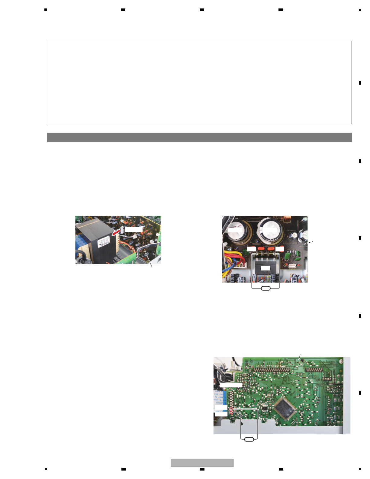
5
1. Discharging
(1) Unplug the power cord.
(2) Disconnect the 10P connector from CP403 of the AMP7/AMP5 Assy between CN3 of the MAIN Assy.
(3) Connect +B and –B terminal of the D7, using resistor leads with 47 - 100 ohms (2 W or higher), for discharging.
∗ Discharging time: 30 - 60 seconds, depending on the level of resistance.
(4) Check that the voltage between the +B and –B terminals is less than 1 V, using a tester.
∗ Be sure to connect the GND terminal of the tester to the chassis.
∗ If the voltage is still 1 V or higher, repeat Step (3).
[1] MAIN Assy Capacitor (C55, C58)
[Procedures]
(1) Unplug the power cord.
(2) Connect pin 1 (–30V) and pin 2 (GND) of CN704B on
the CPU Assy, using resistor leads with 47-100 ohms
(2 W or higher), for discharging.
∗ Discharging time: 5 - 10 seconds, depending on the
level of resistance.
(3) Check that the voltage between the –30V terminal is less
than 1 V, using a tester.
∗ Be sure to connect the GND terminal of the tester to
the chassis.
∗ If the voltage is still 1 V or higher, repeat Step (2).
[2] FL-30 V Capacitor (MAIN Assy C101)
[Procedures]
47 - 100 ohms
(2 W or higher)
47 - 100 ohms
(2 W or higher)
C55
+B
GND
−30V
–B
D7
CP403
C58
Note:
(1) Even if the unit shown in the photos and illustrations in this manual may differ from your product, the
procedures described here are common.
(2) For performing the diagnosis shown below, the following jigs for service is required:
• 9P extension jig cable (GGD1739)
• 13P extension jig cable (GGD1740)
• 3P extension jig cable (GGD1741)
• Board to board extension jig cable (GGD1756)
• Board to board extension jig cable (GGD1770)
• Board to board extension jig cable (GGD1800)
• 25P extension jig FFC (GGD1801)
MAIN Assy
AMP7/AMP5 Assy
CPU Assy
CN704B
6 7 8
7. DISASSEMBLY
A
B
C
D
E
F
VSX-1022-K
5
6 7 8
55
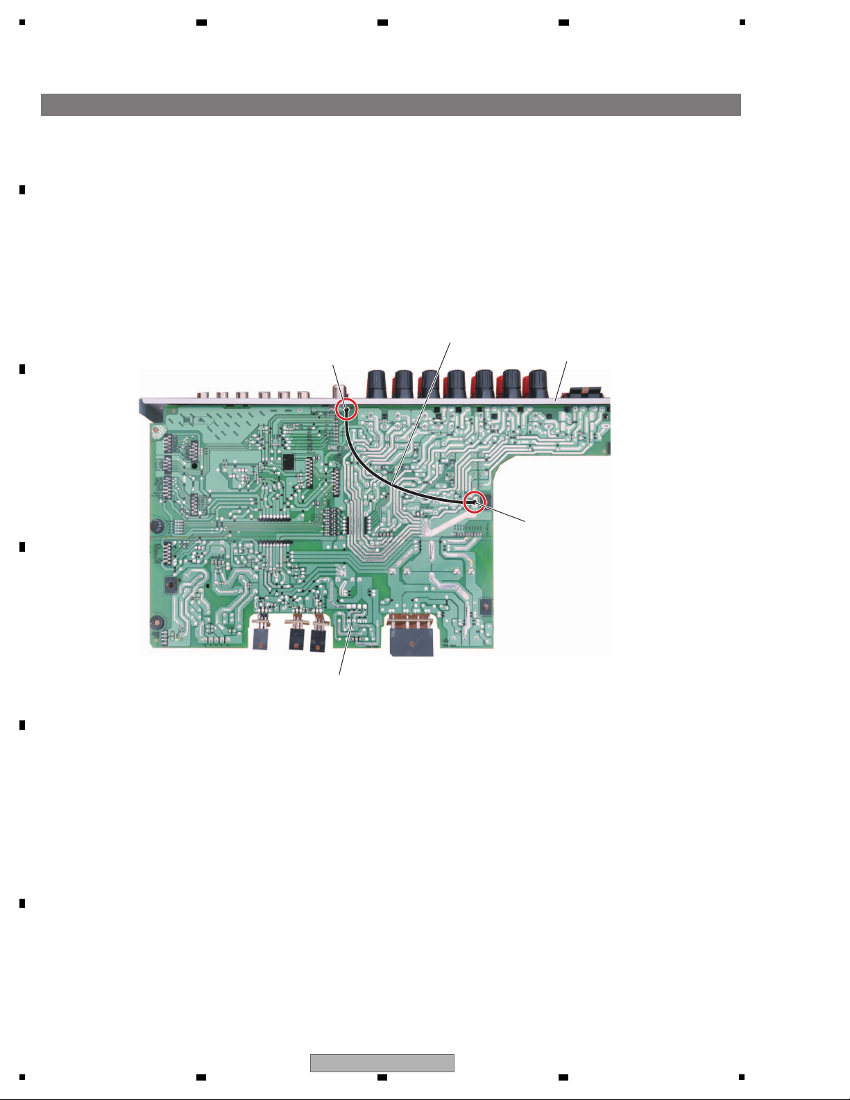
1
2. Notes on Ground Points Connection
During repair, before checking the MAIN Assy, etc., with the rear chassis removed, be sure to connect the
GND terminal of the main capacitor to the back chassis (speaker chassis), as shown below, then connect the
power cord.
Without grounding connection, the protection circuit will be activated.
After repairing, be sure to remove the ground wire before reassembling.
[Note]
MAIN Assy (SIDE B)
Back chassis
GND wire
(Be sure to disconnect the GND wire
before reassembly.)
Main capacitor GND
Speaker chassis
A
2 3 4
B
C
D
E
F
56
1
2 3 4
VSX-1022-K
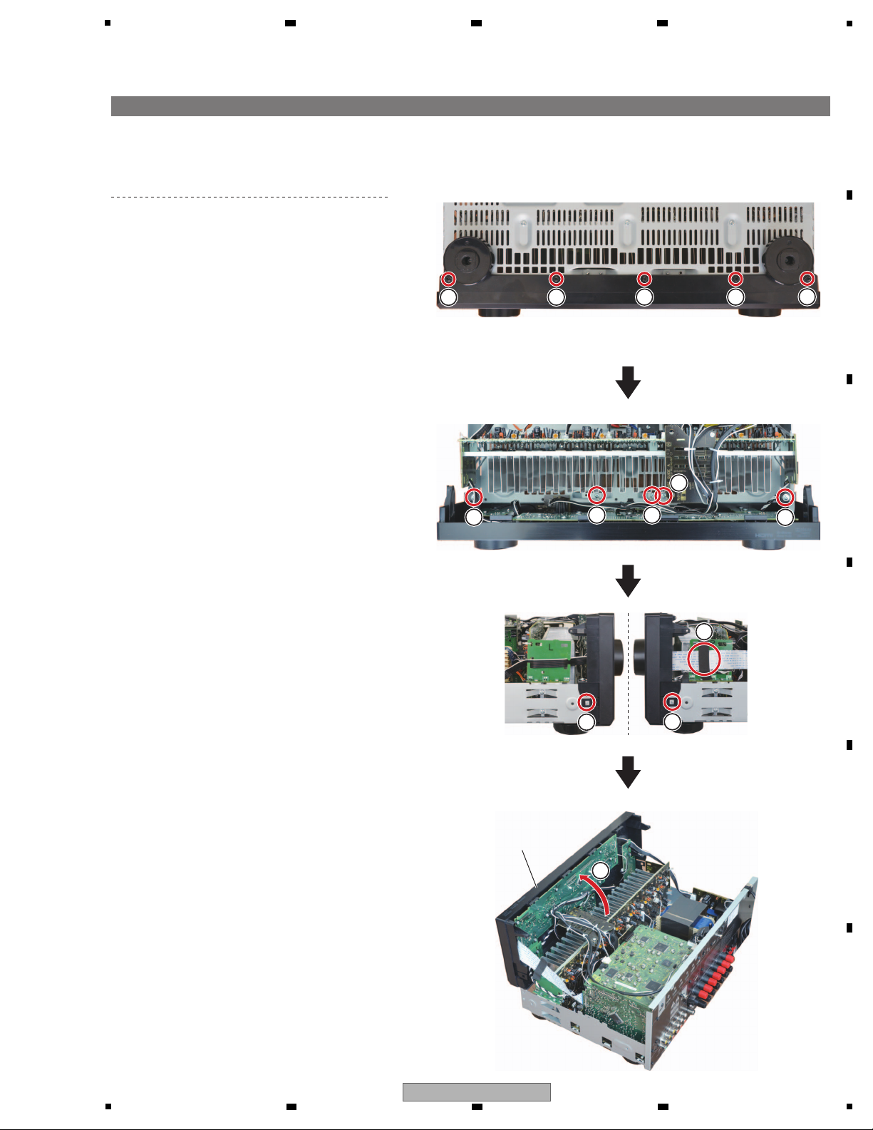
5
3. Disassembly
[1] Front Panel Section
Remove the cabinet by removing the 10 screws.
(1) Remove the five screws. (BBZ30P080FTB)
(2) Remove the two screws.
(BBZ30P080FTC)
(3) Remove the three screws.
(1500001206010-IL)
(4) Remove the tape.
(5) Unhook the two hooks.
(6) Arrange the front panel section as shown
in the photo below.
1
1
1 1
1
3
3
2 2
5
5
4
3
6
• Bottom view
Front panel section
6 7 8
A
B
C
D
5
6 7 8
VSX-1022-K
E
F
57
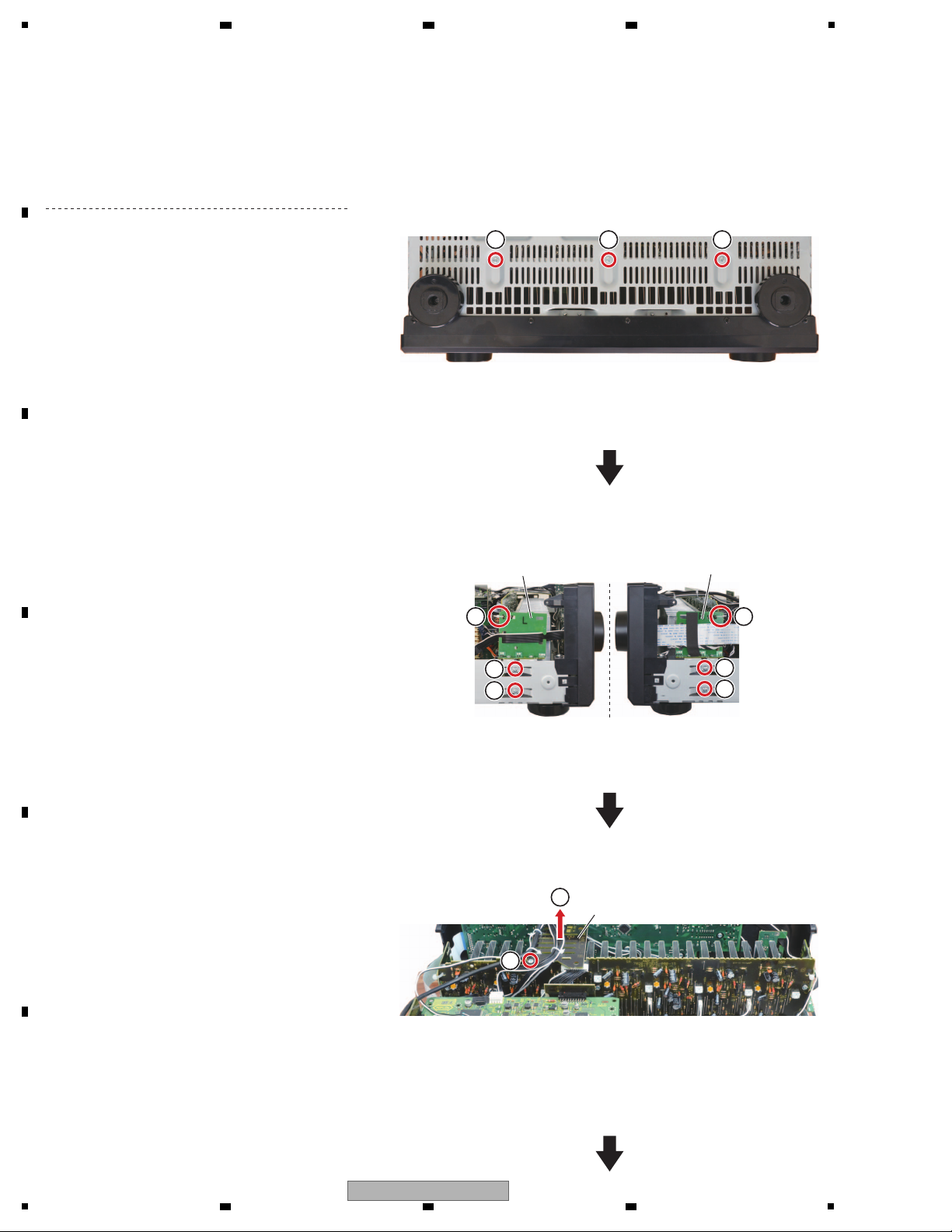
1
[2] Heatsink Section
Remove the cabinet by removing the 10 screws.
Caution: Heatsink section in work becomes hot,
and be careful with it.
(1) Remove the three screws. (BBZ30P080FTC)
(2) Remove the four screws. (BBZ30P080FTC)
(3) Cut the two binders.
(4) Remove the one screw. (BBZ30P080FTC)
(5) Remove the WG-A Assy.
G-L Assy
G-R Assy
1 1 1
2
2
2
2
4
33
• Bottom view
5
WG-A Assy
A
B
2 3 4
C
D
E
F
58
1
2 3 4
VSX-1022-K

5
(9) As shown, arrange the Heatsink section over
the WG-A Assy.
(10) Re-connect the three connectors.
(VSX-1022-K, VSX-42)
(11) Connect the two extension jig cables.
(VSX-1022-K, VSX-42)
Connect the one extension jig cable.
(VSX-822-K)
Note:
AMP5 Assy: GGD1739
AMP7 Assy: GGD1740 + GGD1741
(6) Cut the two binders.
(7) Disconnect the five connectors.
(VSX-1022-K, VSX-42: CP401 to CP405)
Disconnect the four connectors.
(VSX-822-K: CP401 to CP404)
(8) Remove the Heatsink section.
6
AMP7/AMP5 Assy
AMP Assy
CPU Assy
WG-A Assy
(VSX-1022-K,
VSX-42 only)
Heatsink
9
10
10
11
10
CP401
Extension jig cable
(VSX-1022-K, VSX-42: GGD1740)
(VSX-822-K: GGD1739)
11
Extension jig cable
(GGD1741)
(VSX-1022-K, VSX-42 only)
77
7
7
7
CP405
CP403
CP402
CP404
CP401
8
6 7 8
A
B
C
D
E
F
VSX-1022-K
5
6 7 8
59

1
[3] D-MAIN Assy
Remove the cabinet by removing the 10 screws.
(1) Remove the five screws. (BBT30P100FTB)
(2) Remove the seven screws. (BSZ30P040FTB)
(3) Disconnect the three B to B connectors.
(CN101, CN102, CN1401)
(4) Remove the D-MAIN and OPTCO Assemblies.
1
Back chassis
2
1
×7
×4
• Rear view
BRG-A Assy
D-MAIN Assy
D-MAIN Assy
OPTCO Assy
CPU Assy
3
4
3
3
CN101
CN101
CN102
CN102
CN1401
CN1401
CP2003
CN201
CN213
(6) Connect the three extension jig cables.
(7) Arrange the D-MAIN and OPTCO Assemblies
in the photo below.
(8) Insert any insulation sheet.
Note:
9 pin connector on GGD1756 is not used in this
case.
Insulation sheet
OPTCO Assy
8
7
6
Borad to board extension
jig cable (GGD1770)
6
Borad to board extension
jig cable (GGD1800)
6
Borad to board extension
jig cable (GGD1756)
A
2 3 4
B
C
D
E
F
60
1
VSX-1022-K
2 3 4
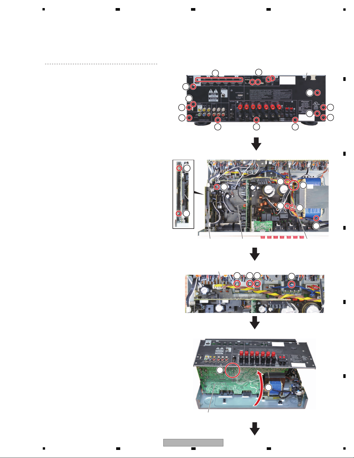
5
[4] MAIN Assy
[4-1] Back chassis, D-MAIN Assy
Remove the cabinet by removing the 10 screws.
(1) Remove the 15 screws. (BBT30P100FTB)
(2) Remove the seven screws. (BSZ30P040FTB)
(3) Remove the D-MAIN Assy.
(See procedure [3].)
Back chassis
2
1
1
1
1
1
1
1
1
1 1 1
1
×7
×4
[4-2] MAIN Assy
(1) Remove the four screws. (BBZ30P180FTC)
(2) Remove the two screws. (BBZ30P080FTC)
(3) Cut the four binders.
1
1
1
1
3
3
2
2
×3
MAIN Assy WG-B Assy
MAIN Assy
CPU Assy
(4) Remove the four screws. (BBZ30P080FTC)
4
444
(5) Arrange the unit as shown in the photo below.
(6) Connect the chassis ground.
See “2. Notes on Ground Points Connection”.
5
6
MAIN Assy
6 7 8
A
B
C
D
E
F
5
6 7 8
VSX-1022-K
61

1
[4-3] Regulator ICs and Recifier diode
(1) Remove the support.
(2) Tighten then loosen the screw in each of the
four holes for temporary joining that are
located on the rear side of the main chassis.
(This is for shaving the thread grooves to
facilitate attachment in the next step.)
Support
Main chassis
Screwdriver
1
2
222
MAIN Assy
3 3 3
3
Note:
While securing the regulator ICs and rectifier diode to the holes for
temporary joining, tighten the screws while holding the regulator ICs
and rectifier diode with your fingers so that the jumper wires will not
become distorted.
(3) Attach the three regulator ICs and a rectifier
diode to the holes tapped in Step (2).
Be sure to place them in a direction
perpendicular to the board and take care that
the jumper wires will not become distorted.
A
B
2 3 4
C
D
E
F
62
1
VSX-1022-K
2 3 4
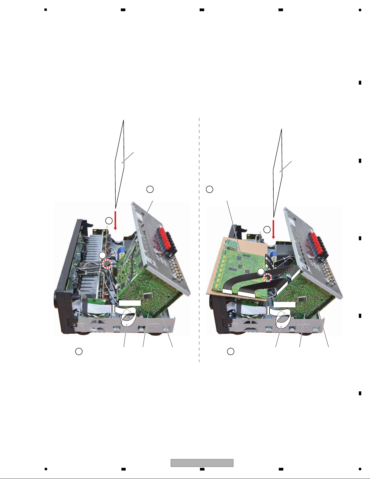
5
[4-4] Diagnosis
(1) Connect the CP401 on the AMP Assy with
extension jig cable. (See procedure [2].)
(2) Reassemble the D-MAIN Assy to the rear
panel or put it on the AMP Assy with
extension jig cables. (See procedure [3].)
(3) Connect the extension jig FFC.
(4) Insert any insulation sheet between AMP
Assy and MAIN Assy.
MAIN AssyCPU Assy MAIN AssyCPU Assy
Insulation sheet
4
Insulation sheet
4
D-MAIN Assy
2
D-MAIN Assy
2
1
1
CN704B
7
Extension jig FFC
(GGD1801)
CN704B
7
Extension jig FFC
(GGD1801)
6 7 8
A
B
C
D
E
F
VSX-1022-K
5
6 7 8
63

1
• If the adjustment is shifted or if it becomes necessary to readjust because of part replacement, etc., perform the
adjustment as described below.
• Any value changed in Adjustment mode will be stored in memory as soon as it is changed. Before readjustment, take note of
the original values for reference in case you need to restore the original settings.
• Use a stable AC power supply.
AMP7/AMP5 Assy "8.3 IDLE CURRENT ADJUSTMENT" (All channel)
Other assemblies No adjustment required
When any of the following assemblies is replaced
AMP7/AMP5 Assy "8.3 IDLE CURRENT ADJUSTMENT"
(Only channel of replacement parts)
Other assemblies
Note:
Some parts on D-MAIN and F-USB Assemblies can not be replaced due to using heat-pad connection between the board.
Please refer to [1.2 NOTES ONREPLACING PARTS], when the parts listed in the table is defective, replace whole Assy.
No adjustment required
When any of the following parts is replaced
2 3 4
8. EACH SETTING AND ADJUSTMENT
A
B
8.1 ADJUSTMENT REQUIRED WHEN THE UNIT IS REPAIRED OR REPLACED
C
D
E
F
64
1
2 3 4
VSX-1022-K

5
[Purpose]
PC
UPDATE jig
GGF1642
Straight Cable Adapter JIG's side
RS-232C
Straight cable
Rear side
(MAIN microcomputer)
10P
10P
Refer to this section when updating the firmware of each microcomputer is required by the service information, etc.
[Necessary Tools and Connections]
• PC with a serial port
• RS-232C cable (9-pin to 9-pin, straight cable) (Marketing product)
• UPDATE jig: GGF1642 (Use FFC of GGF1642. (10P to 10P FFC))
• Firmware
Connect as shown in the figure below.
Insert the FFC with its contact surface facing the " mark.
10P to 10P FFC
(1) MAIN microcomputer firmware update
[Procedures]
1. Unplug the AC cord.
Connect the FFC cable. ( MAIN microcomputer )
Start up application FlashSta on the PC.
[Preestablishment]
• NetworkStandby: OFF
• HDMI Control: OFF
• HDMI StandbyThrough: OFF (North America model only)
3. Press the OK button.
[ if the following messages are displayed ]
Please push the cancel button and press the JIG's
RESET button.
And confirm a connection of FFC.
Please return to procedure 1.
2. Plug the AC cord. (STANDBY mode)
For updating of the MAIN microcomputer, proceed with
the following steps in STANDBY mode.
Select for COM port.
6 7 8
8.2 UPDATING OF THE FIRMWARE
A
B
C
D
5
6 7 8
VSX-1022-K
E
F
65

1
4. Select the update file and enter ID.
1 Selection of upgrade file
1 Select the update file
2 Enter ID.
Select "VSX_1022Mid_Main Ver***.mot"
or "VSX42_Main_Ver0.60.mot"
"VSX_822Mid_Main Ver***.mot" file to
update the MCU.
2 Enter ID.
Enter "ff" in all field.
Press the OK button.
Press the OK button.
3 Press OK button to
go to next step.
5. Set speed update and update the MCU.
Press the OK button.
Set Baud rate to 38400.
2 Update the MCU.
E.P.R=>Erase+Program+Read
2 Update the MCU
Press the E.P.R … button
1 Set speed of update.
1 Set speed of update.
Press OK button.
6. Update Finished MAIN microcomputer.
Press the OK button. Press the Exit button.
Please wait for until this window
disappears.
Push the JIG’s RESET button during
1 sec.
Press the OK button.
Select the 9600 of the Board rate then
press the OK button
If the following messages are displayed, shut the update
program down, and start the update again from step 1.
7. Unplug the AC cord.
Disconnect the FFC cable.
A
2 3 4
B
C
D
E
F
66
1
2 3 4
VSX-1022-K

5
[Procedures]
6. When update is completed, "Completed" is displayed by
TV screen and HDMI LED lights.
* "UPDATE" blinks to FL display and is displayed.
In rare cases, "Completed!" may not be displayed on the
TV screen. In such a case, updating is completed if the
HDMI LED has become lit. Proceed to Step 7.
7. Disconect the AC power cord. (The POWER button does
not respond.) Confirm a version of the firm ware of
SUB microcomputer.
Note:
Because update is not possible again, never unplug the
power cord until the updating process is completed.
1. Turn on the unit.
2. Set a function for a "NETRADIO".
Note:
Without a network connection, "Server Error" will be
displayed on the TV screen. Under this condition, the
Service Menu (menu for updating the SUB microcomputer)
is not accessible. Set the remote control unit supplied with
the unit to Network Function Operation mode then press
the ENTER button so that "Empty" is displayed on the screen.
Then proceed to Step 3.
3. Press the "ESC (A85F)" button on the Service remote
control unit (GGF1381), then press the "+10 (A81F)"
button to enter the service menu (for SUB microcomputer
firmware update menu).
When you press other buttons between "ESC" button and
"+10" buttons, be invalid.
4. Press the "ENTER" button of the remote control unit
supplied with Network Function as the state that you can
operate.
(1) When a product can recognize a file, become the
following indication.
Select "Start", and press the "ENTER" button.
5. Update starts, and "UPDATE" blinks to FL screen and
HDMI LED blinks.
Be approximately 8 minutes for update at time.
(2) SUB microcomputer firmware update
• NetworkStandby: OFF
• HDMI Control: OFF
• HDMI StandbyThrough: OFF (North America model only)
• Connect a unit to TV and HDMI, and the GUI output of the unit performs in a state to appear.
[Preparations]
Save the firmware file to the "root" of empty USB memory.
The file name of the firmware file is "RegM13Sub_V***.bcd". Don't save other files.
(2) When a product cannot recognize a file, become the
following indication. Check on USB memory with a file.
6 7 8
A
B
C
D
E
F
5
6 7 8
VSX-1022-K
67
1
[Procedures]
[Procedures]
1. Select an Input Function that allows reception via Optical input 1 then set the unit to STBY_Off mode.
2. Press the SPEAKERS and STANDBY/ON keys simultaneously to enter DSP UpDate mode. ("DSP UP" is displayed.)
3. When "PLAY" is displayed, playback of the .wav file starts. (Play the file only once. NEVER repeat playback.)
("PLAY" is displayed.)
4. After playback is finished and "ENTER" is displayed, press the ENTER key on the front panel. ("ENTER" is displayed.)
5. "WRITING" is automatically displayed.
6. After writing is completed, "COMPLETE" is displayed.
7. Turn the unit off then confirm that the version has been updated.
(4) DSP firmware update
(5) Check to the firmware version
[Preestablishment]
• NetworkStandby: OFF
• HDMI Control: OFF
• HDMI StandbyThrough: OFF (North America model only)
[Preestablishment]
• NetworkStandby: OFF
• HDMI Control: OFF
• HDMI StandbyThrough: OFF (North America model only)
[Procedures]
1. Select ‘Firmware Update’ from the Network Setup menu. The receiver checks whether the USB memory device inserted
into the USB port on the receiver’s front panel contains updatable software.
2. To update, select ‘Start’.
3. When ‘Updating in progress, don’t unplug!’ is displayed, select ‘OK’.
• If ‘File Not Found’ is displayed, try the following:
- No update file was found on the USB memory device. Store the file in the USB memory device’s root directory.
- Try disconnecting then reconnecting the USB device or storing the update file again. If the error still occurs, try using
a different USB memory device.
4. The software update will start. Please wait. The OSD display will turn off during update and the words ‘UPDATE’ will flash
on the front panel.
5. If ‘COMPLETE’ is displayed, updating is completed. The screen will return automatically to the play screen.
• If ‘FAIL’ is displayed on the front panel display, updating has failed. Try the following:
- Turn the receiver’s power off, then turn it back on and try updating the software again.
- Try disconnecting then reconnecting the USB device or storing the update file again. If the error still occurs, try using
a different USB memory device.
(3) USB (BridgeCo) firmware update
Make sure that the main unit is in STANDBY mode.
Press and hold the "ENTER" and "STANDBY/ON" keys, then press the "ENTER" key to display each UCOM version.
Each time the "ENTER" key is pressed, then indications on the FL display change as follows:
Turn the unit off.
* It may take around 1 minute until the version of the USB microcomputer is displayed.
When be not displayed, wait in the state that turned on the power of the product for
1 minute, and please do it from the first procedure again.
"ENTER" "ENTER" "ENTER" "ENTER" "ENTER" "ENTER"
"ENTER"
MAIN UCOM
MAIN Vx.xx
SUB UCOM
SUB V1.zz
CEC
CEC V1.00
Model name,
Destination
DSP firmware
USB UCOM
All segments
lit.
A
2 3 4
B
C
D
E
F
68
1
2 3 4
VSX-1022-K
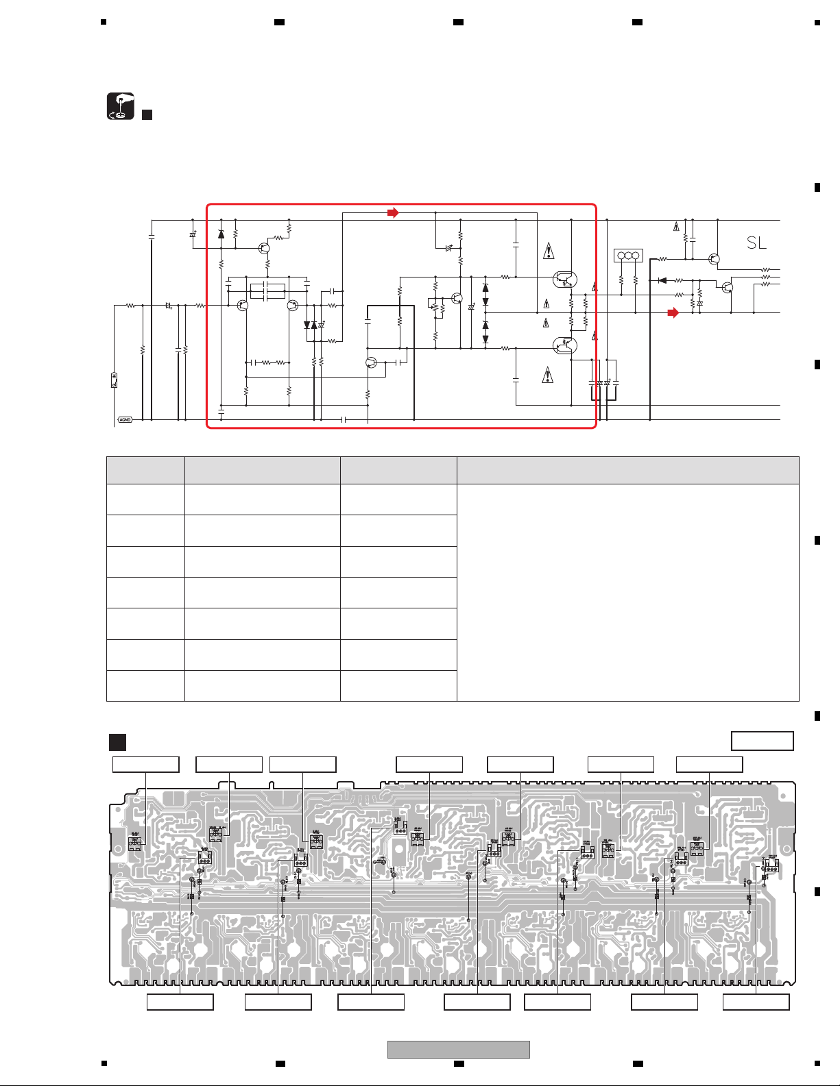
5
560P-50V
C412
-C411
C415
10/100
C405 100P-J
R436
470K
R427
1K2
22/50
C408
C523
100P-100V
C524
100P-100V
R437
22K
R428
1K5
10/50
C522
MTZ5.1A
ZD401
R441
1K2(1)
2N2-K
C413
150
R440
Q407
KSA992F
C409 -
C540 -
R402
100K
R401
1K2
3K3(1)
R434
R429
33K
C568
47P-100V
R703
2K7
R443
47(1)
560
R435
2K7
R432
7K5(1)
R404
C402
100P-500V
R425
0R47(2)
R414
10K
1 32
20010WR-03
TP401
270K
R417
10K
R423
5K6
R426
C409FL
-
R724
-
C401
100N-K
R409
150K
R410
JUMPER
R717 200
R438
200
-
D443-D444
VR401
1K(B)-V
R408
7K5(1)
C407 47/50
C414
100P-500V
R431
0R47(2)
100P-100V
C582
C416 10/100
C581
100P-100V
R406
PRF18BC471QB5RB
R416 22K
C567
47P-100V
R442
JUMPER
C525
-
270
R710
Q412
KTC3206Y
Q408
KSA992F
220P-500V
C406
R420
-
KTC3964
Q409
R422
-
47/50
C404
1SS133T
D404
R439
100(1)
Q410
2SB1560
ZD402
MTZ4.3B
1SS133T
D403
0R47(2)
R424
R413
10K
1SS133T
D402
R419 22K
R412 47K
Q406
2N5551S
C435
-
C410
100/50
R433 -
MTZ4.3B
ZD403
100(1)
R415
Q404
2SD2390
R430
0R47(2)
R411
150K
Q403
2N5401S
Q401
KTA1024Y
(SL)
(SL)
• Adjustment points and measurement points.... see fig.1.
AMP7 ASSY
Fig.1
B
for VSX-1022-K, VSX-42
Adjustment
Points
Procedure
Measurement
Points
Channel
TP404 pin 1 (+)
TP404 pin 3 (–)
1 Turn on the power.
2 Perform aging for one minute.
3 Connect a digital voltmeter to the measurement point.
4 Turn the adjustment VR so that the voltage becomes
in 2.0 mV ± 0.2 mV.
(Condition : No signal and no load)
VR404
TP402 pin 1 (+)
TP402 pin 3 (–)
VR402
TP403 pin 1 (+)
TP403 pin 3 (–)
VR403
TP401 pin 1 (+)
TP401 pin 3 (–)
VR401
TP405 pin 1 (+)
TP405 pin 3 (–)
VR405
FL
FR
C
SL
SR
TP406 pin 1 (+)
TP406 pin 3 (–)
VR406
TP407 pin 1 (+)
TP407 pin 3 (–)
VR407
SBL
SBR
SIDE A
SL_VR401 FL_VR404 SR_VR405 FR_VR402 SBL_VR406 SBR_VR407C_VR403
SL_TP401 FL_TP404 C_TP403 SR_TP405 FR_TP402 SBL_TP406 SBR_TP407
When any component parts which are within the red square on the following circuit diagram are replaced, the idle current
adjustment of that channel is required. (Idle current adjustment for another channel is not required.)
However, when any capacitors are replaced, the adjustment is not required.
(The following circuit diagram is for SL channel, but another channel also has same circuit diagram and same adjustment is
required)
6 7 8
8.3 IDLE CURRENT ADJUSTMENT
A
B
C
D
E
5
6 7 8
VSX-1022-K
F
69

1
(SL)
(SL)
• Adjustment points and measurement points.... see fig.2.
AMP5 ASSY
Fig.2
B
SIDE A
Adjustment
Points
Procedure
Measurement
Points
Channel
TP401 pin 1 (+)
TP401 pin 3 (–)
1 Turn on the power.
2 Perform aging for one minute.
3 Connect a digital voltmeter to the measurement point.
4 Turn the adjustment VR so that the voltage becomes
in 2.0 mV ± 0.2 mV.
(Condition : No signal and no load)
VR401
TP402 pin 1 (+)
TP402 pin 3 (–)
VR402
TP403 pin 1 (+)
TP403 pin 3 (–)
VR403
TP404 pin 1 (+)
TP404 pin 3 (–)
VR404
TP405 pin 1 (+)
TP405 pin 3 (–)
VR405
FL
FR
C
SL
SR
FL_VR401
SL_VR404 C_VR403 SR_VR405 FR_VR402
FL_TP401 SL_TP404 C_TP403 SR_TP405 FR_TP402
When any component parts which are within the red square on the following circuit diagram are replaced, the idle current
adjustment of that channel is required. (Idle current adjustment for another channel is not required.)
However, when any capacitors are replaced, the adjustment is not required.
(The following circuit diagram is for SL channel, but another channel also has same circuit diagram and same adjustment is
required)
for VSX-822-K
A
2 3 4
B
C
D
E
F
70
VSX-1022-K
1
2 3 4

5
6 7 8
A
B
C
D
E
F
VSX-1022-K
5
6 7 8
71

1
NOTES: - Parts marked by “NSP” are generally unavailable because they are not in our Master Spare Parts List.
-
The > mark found on some component parts indicates the importance of the safety factor of the part.
Therefore, when replacing, be sure to use parts of identical designation.
-
Screws adjacent to b mark on product are used for disassembly.
-
For the applying amount of lubricants or glue, follow the instructions in this manual.
(In the case of no amount instructions, apply as you think it appropriate.)
Poly bag packing style
Cord AC
Tape (clear)
Dry cell batteries (AAA size IEC R03)
Sheet SP caution
Safety Brochure
Label getter “R”
Label getter “L”
1/2
2/2
2 3 4
9. EXPLODED VIEWS AND PARTS LIST
A
9.1 PACKING SECTION
B
C
D
E
F
72
1
2 3 4
VSX-1022-K

5
(1) PACKING SECTION PARTS LIST
Mark No. Description Part No.
1 Remote Control See Contrast table (2)
2 AM Loop Antenna E601019000010-IL
3 FM Wire Antenna E605010140010-IL
4 Microphone APM7010
(for Auto MCACC setup)
5 iPod Cable L308102013030-IL
6 Operating Instructions See Contrast table (2)
(CD-ROM)
7Quick Start Guide See Contrast table (2)
8 Box, Gift See Contrast table (2)
6 7 8
A
9Cushion, Snow VSX-522 6230213144000-IL
10 PE, Sheet 6327040059000-IL
NSP 11 Warranty Card See Contrast table (2)
NSP 12 Label VRW1629
(2) CONTRAST TABLE
VSX-1022-K/CUXESM, VSX-42/UXECB and VSX-822-K/CUXESM are constructed the same except for the following:
Mark No. Symbol and Description
VSX-1022-K
/CUXESM
1 Remote Control 8300766100010-IL 8300766200010-IL 8300766100010-IL
6 Operating Instructions (CD-ROM) 6517000000490-IL 6517000000510-IL 6517000000490-IL
7Quick Start Guide 5707000006490-IL 5707000006500-IL 5707000006490-IL
8 Box, Gift 6007212070050-IL 6007212070060-IL 6007212070090-IL
NSP 11 Warranty Card ARY7156 ARY7007 ARY7156
VSX-42
/UXECB
VSX-822-K
/CUXESM
B
C
D
E
F
VSX-1022-K
5
6 7 8
73
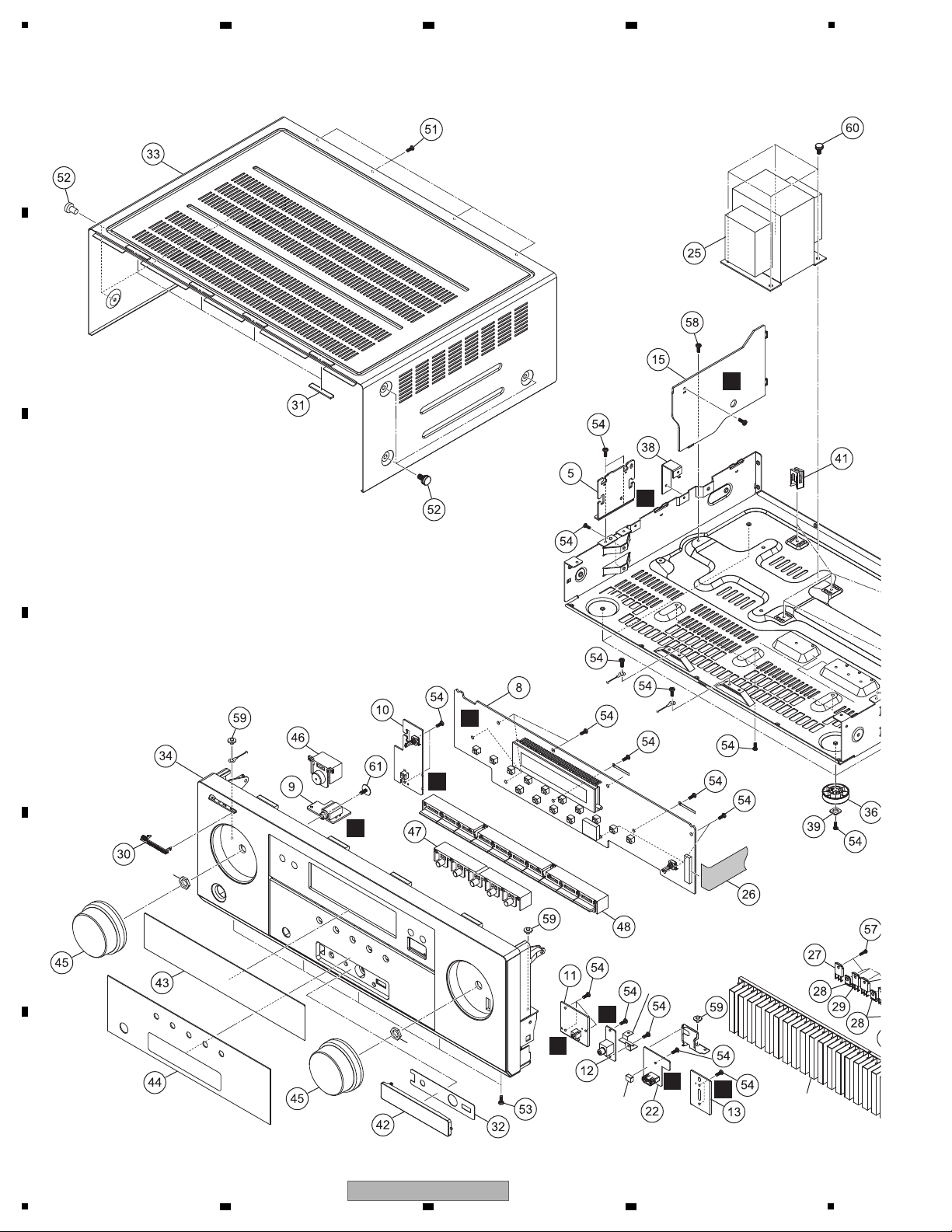
1
fo
VS
S
P
T
U
V
R
Q
G
W
Nut
Nut
Heatsink
Shield plate F
Shield plate F
9.2 EXTERIOR SECTION
A
B
2 3 4
C
D
E
F
74
1
2 3 4
VSX-1022-K

5
CONTACT SIDE
NON-CONTACT
SIDE
Silicon grease
(GEM1057)
for
VSX-1022-K, VSX-42
for
VSX-1022-K, VSX-42
for
VSX-822-K
VSX-822-K
only
for
VSX-822-K,
Silicon adhesive
(GYA1011)
A
D
L
E
F
N
J
H
C
K
O
M
B
I
I
B
Main chassis
Sheet speaker
Stopper
×
30
Sheet speaker
6 7 8
A
B
C
D
5
E
F
VSX-1022-K
6 7 8
75

1
2 3 4
(1) EXTERIOR SECTION SECTION PARTS LIST
Mark No. Description Part No.
1 MAIN Assy See Contrast table (2)
A
2 BTCNT Assy 7028071612050-IL
3 OPTCO Assy 7028071613050-IL
4 G-R Assy 7028071614050-IL
5 G-L Assy 7028071615050-IL
No. Description Part No.
Mark
46 Button See Contrast table (2)
47 5 Key Button 5090214561000-IL
48 10 Key Button 5090214571000-IL
49 Shield AMP PCB See Contrast table (2)
50 • • • • •
6 WG-A Assy 7028071616050-IL
7 WG-B Assy 7028071617050-IL
8 FRONT Assy See Contrast table (2)
9 HP Assy See Contrast table (2)
10 INSEL Assy See Contrast table (2)
B
11 MIC Assy 7028071624050-IL
12 FVIDEO Assy See Contrast table (2)
13 WG Assy 7028071627060-IL
14 VIDEO Assy See Contrast table (2)
15 STBY Assy See Contrast table (2)
16 BRG-1 Assy 7028071673030-IL
17 BRG-2 Assy See Contrast table (2)
18 AUDIO Assy See Contrast table (2)
19 D-MAIN Assy See Contrast table (2)
C
20 CPU Assy See Contrast table (2)
21 AMP Assy See Contrast table (2)
22 F-USB Assy 7028071781030-IL
23 BT Assy 7028070231010-IL
> 24 Cord Assy L068125101710-IL
> 25 Power Trans See Contrast table (2)
51 Screw BBT30P100FTB
52 Screw BBT40P080FTB
53 Screw BBZ30P080FTB
54 Screw BBZ30P080FTC
55 Screw BBZ30P180FTC
56 Screw BSZ30P040FTB
57 Screw Tapping Assy B018230141H11-IL
58 Screw, Tap Tite B020230063B10-IL
59 Screw, Tap Tite 1500001206010-IL
60 Screw B028940101B11-IL
61 Screw 1500001456010-IL
26 Cable Flat Card 1.0 N711251722480-IL
> 27 Transistor J5011560Y0000-IL
> 28 Semi, Tr/Ge NPN 2SC J502396400010-IL
> 29 Transistor J5032390Y0000-IL
D
30 Pioneer Badge See Contrast table (2)
31 Sheet 1210210235000-IL
32 F Input Sheet See Contrast table (2)
33 Cabinet VSX-522 3007212006000-IL
34 Front Panel See Contrast table (2)
35 Back Chassis See Contrast table (2)
36 Foot (PLS) 4000210391000-IL
37 Bracket 4010056906010-IL
E
38 Bracket SMPS 4010214886000-IL
39 Cushion 4050211605000-IL
40 Screw Cover 4050211745100-IL
41 Support 4070001601010-IL
42 Front Input Cover 4317215111030-IL
43 Window Display U See Contrast table (2)
44 Window Lo
wer
See Contrast table (2)
45 Knob 5080212431000-IL
F
76
1
2 3 4
VSX-1022-K

5
6 7 8
(2) CONTRAST TABLE
VSX-1022-K/CUXESM, VSX-42/UXECB and VSX-822-K/CUXESM are constructed the same except for the following:
Mark No. Symbol and Description
VSX-1022-K
/CUXESM
1 MAIN Assy 7028071611030-IL 7028071611050-IL 7028071611010-IL
8 FRONT Assy 7028071621030-IL 7028071621050-IL 7028071621030-IL
9 HP Assy 7028071622030-IL 7028071622050-IL 7028071622030-IL
10 INSEL Assy 7028071623030-IL 7028071623050-IL 7028071623030-IL
12 FVIDEO Assy 7028071626030-IL 7028071626050-IL 7028071626030-IL
14 VIDEO Assy 7028071671030-IL 7028071671030-IL 7028071671010-IL
15 STBY Assy 7028071672030-IL 7028071672030-IL 7028071672010-IL
17 BRG-2 Assy 7028071674030-IL 7028071674050-IL 7028071674030-IL
18 AUDIO Assy 7028071641030-IL 7028071641050-IL 7028071641010-IL
19 D-MAIN Assy 7028071691050-IL 7028071691050-IL 7028071691010-IL
20 CPU Assy 7028071681030-IL 7028071681050-IL 7028071681010-IL
21 AMP7 Assy 7028070253010-IL 7028070253010-IL Not used
21 AMP5 Assy Not used Not used 7028070245010-IL
> 25 Power Trans 8200960611140-IL 8200960611140-IL 8200960611180-IL
30 Pioneer Badge XAM3006 PAM1791 XAM3006
32 F Input Sheet 1217211792000-IL 1217211792010-IL 1217211792000-IL
34 Front Panel 3067215491010-IL 3067215501000-IL 3067215491020-IL
35 Back Chassis 3207214196000S-IL 3207214196200S-IL 3207214186000S-IL
43 Window Display U 5077213113020-IL 5077213113030-IL 5077213113020-IL
44 Window Lower 5077213123060-IL 5077213123040-IL 5077213123060-IL
VSX-42
/UXECB
VSX-822-K
/CUXESM
A
B
C
46 Button 5090213741100-IL 5098214551000-IL 5090213741100-IL
49 Shield AMP PCB Not used Not used 4010215676000-IL
D
E
F
VSX-1022-K
5
6 7 8
77

1
C417
47N-K
470K
R478
680P-J
C511
R513
47K
100/16
C432
10/50
C433
2K2
R564
10/50
C541
R592
-
C506
10/50
C492 10/50
LUG401
NM
-
R406
R572
10K
C519
-
C520 -
R562
-
470K
R565
C540
220P-J
330
R590
C539
100P-J
330
R541
C505
220P-J
R593
330
C504
100P-J
R532
330
330
R530
220P-J
C494
R521
330
C493
100P-J
C465
100P-J
C457
-
R470
0
-
C470
R400
100
100P-J
C402
C403
-
R591
470K
R537
-
C542 10/50
R527
-
R533
-
10/50
C498
C499 10/50
R528
470K
R534
470K
-
R522
R523
470K
R463
10K
C476
-
1K
R462
R419
2K
R408
10K
2K
R402
C490
-
10K
R413
R465
-
C408
10/50
10/50
C460
10/50
C400
R473
0
47/10
C468
10N-K
C533
R568
10K
C522
-
47K
R481
100
R472
R469
100
R509
0
C517 -
C479
100P-J
100(1)
R588
10N-K-2012
C515
C507
10/50
ZD401
MTZ6.8B
C558-C566
-
Q428
2SK492C
1K5
R554
R539
4K7
C503
R503 0
R512
470
R491
0
C441
10N-K-2012
R589
100(1)
RT1P141C
Q426
C411
47N-K
R422
4K7
10K
R613
C475
10/50
R497
1K
C412
47N-K
C413
47N-K
C486
10/50
C485
10N-K
0
R518
C414
47N-K
C415
47N-K
R500
0
C418
47N-K
C502
220P-J
C544
220P-J
C543
100P-J
C501
100P-J
C497
220P-J
C496
100P-J
R417
100
C404
100P-J
R461
100
-
C405
Q416
INC2001AC1
R595
R594
470K
INC2001AC1
Q417
C487
-
R411
-
C467
47/10
47K
R485
R516
0
R576
10K
C534
10N-K
C512
3N3-K
R549
100K
R561
10K
R520
470
470
R517
100P-J
C482
R577
-
R477
470K
10N-K-2012
C473
4K7
R447
C546
330P-J
C547
330P-J
R551
100K
Q427
RT1N441C
1/50
C516
R542
0
C425
150N(R)-63V
47N(EB)-100V
C424
100/16
C429
100/16
C428
100/16
C431
10/50
C430
10/50
C434
8
4
5
6
3
2
1
7
IC403
Q425
2SK492C
470K
R610
R583
470K
10/50C462
J501
0
R405
47K
R559
10K
C448 47N(EB)-100V
R468
10K
C472
-
1K
R466
470K
R582
470K
R609
C529
10N-K-2012
C514
10N-K-2012
R538
470K
10/50
C488
10/50
C464
47K
R467
C459
10N-K-2012
C469
0
J500
0
R601
0
ZD400
MTZ6.8B
220/16(6.3*11)
C537
10N-K-2012
C528
D415
LBAS16HT1G
91K
R571
10K
R573
R574
10K
R557
91K
10K
R560
R544
1K
R540
4K7
C508
10N-K
R511 470
100P-J
C477
C480
100P-J
10K
R505
C449 22N(EB)-100V
R459
0
R479
-2012
R515
3K9
C416
47N-K
JACK402
JACK403
10/50
C489
R416
47K
10N-K-2012
C466
J502
0
R598
0
220/16(6.3*11)
C538
R548
5K6
C509
10/50
D414
LBAS16HT1G
C427
100/16
C447 150N(R)-63V
22N(EB)-100V
C423
R507
1K5
C4811N-K
C484
47P-J
JACK401
R566
10K
R569
10K
5
6
8
7
1
4 3
2
UTC4580
UTC4580
UTC4580
IC401
INC2001AC1
Q401
INC2001AC1
Q404
98
97
96
95
94
93
92
91
90
89
88
87
86
85
84
432 1
99
83
82
81
80
797877767574737271706968676665646362616059585756555453
5251
50
49
48
5678
910111213141516
1718
192021
22
35
36
37
38
39
40
41
42
43
44
45
46
47
23
242526
2728
2930
31
32
33
34
IC400
R2A15218FP
8
4
5
6
3
2
1
7
IC402
A
C
CP17
(FL)
(FL)
: Audio Signal Route (Front L ch)
(SL)
: Audio Signal Route (Surround L ch)
(C)
: Audio Signal Route (Center ch)
(SW)
(SW)
: Audio Signal Route (SubWoofer ch)
(TU)
: Audio Signal Route (Tuner L ch)
(TU)
(TU)
(CD)
: Audio Signal Route (CD L ch)
(CD)
(CD)
(SBL)
: Audio Signal Route (Surround Back L ch)
(FL)
(FL)
(SW)
(SL)
(C)
(SBL)
(SW)
(SW)
(SW
(SW)
(FL)
(SL)
(C)
(SW)
(SBL)
(SBL)
(SBL)(SBL)
(HP)
: Audio Signal Route (Headphone L ch)
: Audio Signal Route (L ch)
10. SCHEMATIC DIAGRAM
10.1 AUDIO ASSY
A
B
C
D
E
F
78
1
2 3 4
VSX-1022-K
2 3 4
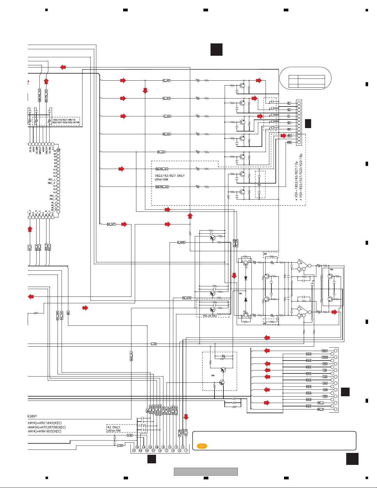
5
C417
47N-K
100/16
C432
10/50
C433
R403
220K
R401
220K
R498
4K7
R506
4K7
R536
10K
470K
R531
R429
47K
OTHER 100pF/50V CH
100pF/50V CH
R500
0
C418
47N-K
C535
10N-K
C536
10N-K
R502
-
C463
10/50
C439
10/50
C420
10/50
C401
10/50
10K
R614
2K2
R570
470K
R597
C545
100N-K
0.22U/25V
C500
C478 0.22U/25V
R514
10K
470
R508
R471
1K5
R458
1K5
R433
1K5
R427
1K5
R404
1K5
2SK492C
Q435
R495
0
R484
47K
R474
10K
-
C564
R449
47K
R448
10K
-
C563
R435
10K
-
C561
INC2001AC1
Q407
-
C562
R420
10K
R421
47K
-
C560
R410
47K
INC2001AC1
Q402
-
C559
R409
10K
R488
1K
-
C554
-
C555
R423
10K
R487
1K
R499
0
1/50
C444
C442
100P-J
R596
220
C550
82P-J
5K6
R493
220
R586
C551
82P-J
SYXCN5
JXCN
R543
0
470/16
C437
470/16
C440
-
C556
-
C557
10/50
C434
C454
10/50
C406
10/50
C446
10/50
1K5
R415
R444
1K5
R496
0
D416
LBAS16HT1G
D417
LBAS16HT1G
Q433
2SK492C
R460
10K
INC2001AC1
Q413
-
C565
R464
47K
R428
10K
INC2001AC1
Q405
INC2001AC1
Q410
220K
R475
220K
R476
R414
10K
INC2001AC1
Q415
R504
0
C438
100P-J
C421
220P-J
5K6
R490
C410
220P-J
10N-K-2012
C569
R425
10K
10K
R424
470K
R501
***************************************
***************************************
C416
47N-K
C570
CH10P-D
C548
CH10P-D
J402
NM
J416
0
J415
0
Q434
RT1N441C
470K
R567
C518
1/50
R600
10K
Q429
RT1P141C
R599
100
C436
1/50
C443
1/50
R535
470
1/50
C422
Q419
RT1P141C
INC2001AC1
Q418
R436
47K
R529
0
R489
22K
R587
33(1)
C553
100P-J
C568
10N-K-2012
33(1)
R510
C407,C409,C419,C426,C435
ALL DESTINATION:100pF/50V CH
1K5
C484
47P-J
C125Z2-17
CN402
C549
CH10P-D
C571CH10P-D
RT1P141C
Q432
Q421
RT1P141C
INC2001AC1
Q414
R602
0
INC2001AC1Q406
C552
100P-J
22K
R492
Q422
INC2001AC1
INC2001AC1
Q420
4 3 126 578910111213
CN400
2.0MM-13P
324
5
6 8
7
1
IC406
10 8 6 4 2
3579 119
1618 14 12
111317 15
CN403
C125Z2-19
UTC4580
C409
100P-J
100P-J
C419
100P-JC426
C407
100P-J
100P-J
C435
98
97
96
95
94
93
92
91
90
89
88
87
86
85
84
432 1
99
83
82
81
80
79787776757473
5678
A
A
AUDIO ASSY
M
CP403
N
CP402
B
1/2
CP401
-
When ordering service parts, be sure to refer to "EXPLODED VIEWS and PARTS LIST" or "PCB PARTS LIST".
-
The > mark found on some component parts indicates the importance of the safety factor of the part.
Therefore, when replacing, be sure to use parts of identical designation.
-
: The power supply is shown with the marked box.
(VSX-1022-K: 7028071641030-IL)
(VSX-42: 7028071641050-IL)
(VSX-822-K: 7028071641010-IL)
(CD)
(FL)
(SL)
(C)
(SW)
(SBL)
(FL)
(FL)
(SL)
(SL)
(C)
(C)
(SW) (SW)
(SW)
(SW)
(SW)
(SW)
(SBL)
(SBL)
(SBL)
(HP)
(HP)
(HP)
(HP)
(HP)
(HP)
6 7 8
A
B
C
D
E
F
79
5
VSX-1022-K
6 7 8
1
560P-50V
C412
C460
560P-50V
-C411
C415
10/100
560P-50V
C444
10/100
C447
C556 -
C551 -
-C560
-C559
C405 100P-J
C527
-
C528
C526
-
100P-J
C521
C473 100P-J
C489100P-J
100P-JC505
C441 100P-J
R514
1K2
22/50
C440
C597
NM
R436
470K
R427
1K2
22/50
C408
C523
100P-100V
C536
100P-100V
R515
1K5
C535
10/50
R496
150K
150K
R539
C538
10/50
C524
100P-100V
R437
22K
R428
1K5
10/50
C522
MTZ5.1A
ZD401
2N2-K
C445
150
R527
Q431
KSA992F
C437 100P-J
R497
JUMPER
R571
1K2(1)
R540
JUMPER
100P-JC453
R532
100K
R531
1K2
R441
1K2(1)
2N2-K
C413
150
R440
Q407
KSA992F
C409 -
C540 -
R402
100K
R401
1K2
R719 200
R525
200
R516
33K
R559
33K
3K3(1)
R564
-D449
-D450
3K3(1)
R434
R429
33K
C568
47P-100V
R703
2K7
R573
47(1)
C459
-
R443
47(1)
VR403
1K(B)-V
C451
-
R563
-
VR404
1K(B)-V
R565
560
R560
2K7
560
R435
2K7
R432
C439
47/50
R495
7K5(1)
R538
7K5(1)
7K5(1)
R404
100P-500V
C433
C462
100P-500V
C402
100P-500V
R512
0R47(2)
R518
0R47(2)
100P-100V
C588
C463
10/100
R555
0R47(2)
R562
0R47(2)
R425
0R47(2)
C457 100P-J
C520 100P-J
C534
100P-100V
C539
100P-100V
R557
1K2
22/50
C456
R566
470K
C542
100P-100V
ZD407
MTZ5.1A
R558
1K5
R567
22K
MTZ5.1A
ZD410
C579
47P-100V
R409
150K
R528
1K2(1)
R490
100K
R488
1K2
Q443
KSA992F
2N2-K
C461
150
R570
270
R716
R410
JUMPER
R705
2K7
-D448
-
D447
C572
47P-100V
R720 200
R568 200
C580
47P-100V
R717 200
R438
200
-
D443-D444
R530
47(1)
C443
-
R519
2K7
R522
560
VR401
1K(B)-V
R489
7K5(1)
R534
7K5(1)
C455
47/50
R408
7K5(1)
C407 47/50
100P-500V
C446
C449
100P-500V
C414
100P-500V
100P-100V
C585
R431
0R47(2)
100P-100V
C582
C416 10/100
R523
470K
R524
22K
C448 10/100
C537
-
100/50
C442
C543
-
100/50
C458
GND1
CHASSIS_BKT1
GND3
C598
NM
C567
47P-100V
C467
-
270
R712
Q436
KTC3206Y
Q432
KSA992F
-
R507
R509
-
C436
47/50
R572
JUMPER
R552
-
220P-500V
C454
R706
2K7
R442
JUMPER
C525
-
270
R710
Q412
KTC3206Y
Q408
KSA992F
220P-500V
C406
R420
-
KTC3964
Q409
R422
-
47/50
C404
100(1)
R526
D415
1SS133T
ZD409
MTZ4.3B
0R47(2)
R511
0R47(2)
R517
100(1)
R502
C464 10/100
MTZ4.3B
ZD412
1SS133T
D422
0R47(2)
R554
0R47(2)
R561
100(1)
R545
ZD411
MTZ4.3B
2SD2390
Q440
1SS133T
D404
R439
100(1)
Q410
2SB1560
ZD402
MTZ4.3B
1SS133T
D403
0R47(2)
R424
R413
4 3 126 578910111213
CP401
20010WS-13
C571
47P-100V
R529
JUMPER
3K3(1)
R521
C438
220P-500V
R520
-
KTC3964
Q433
Q444
KSA992F
Q448
KTC3206Y
-
R550
47/50
C452
Q445
KTC3964
C435
-
C410
100/50
R433 -
ZD408
MTZ4.3B
D416
1SS133T
2SD2390
Q428
D421
1SS133T
100(1)
R569
Q446
2SB1560
MTZ4.3B
ZD403
100(1)
R415
Q404
2SD2390
R430
0R47(2)
Q434
2SB1560
Q425
KTA1024Y
Q401
KTA1024Y
Q437
KTA1024Y
B
1/2
AMP7 ASSY (7028070253010-IL)
A
CN400
B
2/2
(FL)
(FL)
(SL)
(SL)
(C)
(C)
(SBL)(SBL)
2 3 4
10.2 AMP7 ASSY (1/2)(VSX-1022-K, VSX-42)
A
B
C
D
E
F
80
1
2 3 4
VSX-1022-K
R541
150K
10K
R510
270K
R504
C415
10/100
R736-R735 -
10/100
C447
R464
-
R512
0R47(2)
R518
0R47(2)
100P-100V
C588
C463
10/100
R555
0R47(2)
R562
0R47(2)
R425
0R47(2)
C587
100P-100V
R543
10K
R544
10K
R414
10K
132
20010WR-03
TP401
R513
5K6
R726
-
C409C
-
C434
100N-K
R556
5K6
270K
R547
270K
R417
10K
R423
5K6
R426
C409FL
-
R724
-
C401
100N-K
C531
10/100
Q417
KSA992F
4R7(1)
R493
C425
-
D457
-
R449
-
R734
-
100P-100V
C585
R431
0R47(2)
100P-100V
C582
C416 10/100
R501
10K
1 3
2
20010WR-03
TP404
C581
100P-100V
C450
100N-K
10K
R553
R727
-
Q442
2N5551S
10N-KC403
R407 10K
330/6.3(6.3*11)
C513
C514
330/6.3(6.3*11)
C516-C517
-
R732
10K
5678910 4 3 2 1
20010WS-10
CP403
C448 10/100
R536 1K2
C515
47/10
123456
CN404
CNT-5P
R406
PRF18BC471QB5RB
R506 22K
R499 47K
R549 22K
R542 47K
R416 22K
0R47(2)
R511
0R47(2)
R517
R494
PRF18BC471QB5RB
150K
R498
1 32
TP403
20010WR-03
C464 10/100
0R47(2)
R554
0R47(2)
R561
2SD2390
Q440
1SS133T
D420
Q410
2SB1560
0R47(2)
R424
R413
10K
1SS133T
D402
Q430
2N5551S
Q427
2N5401S
R503 22K
Q439
2N5401S
R546 22K
C419
100/100
R419 22K
R412 47K
Q406
2N5551S
R421
22K
D458
-
R733
-
C586
100P-100V
2SD2390
Q428
R500
10K
1SS133T
D414
R537
PRF18BC471QB5RB
Q446
2SB1560
Q404
2SD2390
R430
0R47(2)
R411
150K
-
C409SL
R551
100(1)
Q403
2N5401S
R731
10K
Q434
2SB1560
Q405
2N5401S
C
CN1
C
CN3
E
CP404
B
2/2
(FL)
: Audio Signal Route (Front L ch)
(SL)
: Audio Signal Route (Surround L ch)
(C)
: Audio Signal Route (Center ch)
(FL)
(FL)
(SL)
(SL)
(C)
(C)
(SBL)
: Audio Signal Route (Surround Back L ch)
5
6 7 8
A
B
C
D
E
F
VSX-1022-K
5
6 7 8
81

1
R480
470K
560P-50VC492
R481
22K
R721
200
R482200
47/50
C423
C512
10/100
560P-50V
C508
R723 200
R722 200
-D451
C496
10/100
C432
10/100
R640
0R47(2)
R639
10K
C554
100P-100V
1K2
R643
C549
100P-100V
1K2
R471
C529
100P-100V
1K2
R600
10/50
C555
22K
R653
R644
1K5
10/50
C550
R472
1K5
22/50
C424
10/50
C530
C595
NM
R601
1K5
22/50
C472
R700
1K2(1)
R661
100K
R657
1K2(1)
C600
NM
2N2-K
C493
R618
100K
C596
NM
2N2-K
C429
R446
100K
2N2-K
C477
Q455
KSA992F
R701
JUMPER
-D455
-D456
C574
47P-100V
1K2
R660
R709
2K7
R658
JUMPER
270
R714
C576
47P-100V
R617
1K2
R708
2K7
270
R711
R718 200
Q420
KSA992F
R444
1K2
R704
2K7
270
R715
R611 200
C507
-
C553 -
33KR645
C533 -
3K3(1)
R478
R473
33K
C548 -
R602
33K
R692
-
-
R679
R636
-
C499
-
R463
-
C483
-
-
R593
7K5(1)
R667
R663
7K5(1)
KTC3964
Q469
R638
-
7K5(1)
R620
C484
47/50
Q421
KTC3964
R465
-
R445
7K5(1)
C420
47/50
R451
7K5(1)
R595
-
C471
47/50
R581
7K5(1)
47/50
C468
C510
100P-500V
100(1)
R674
C497
100P-500V
R655
100(1)
R631
100(1)
100P-500V
C481
R483
100(1)
1SS133T
D410
D409
1SS133T
MTZ4.3B
ZD405
C417
100P-500V
C478
100P-500V
100(1)
R612
1SS133T
D427
MTZ4.3B
ZD415
100(1)
R588
C465
100P-500V
0R47(2)
R689
2SD2390
Q476
Q470
2SB1560
Q422
2SB1560
0R47(2)
R467
R474
0R47(2)
0R47(2)
R597
0R47(2)
R603
C594
100P-100V
10/100C511
10K
R672
10K
R629
132
TP406
20010WR-03
1 32
TP402
20010WR-03
C590
100P-100V
R682
10K
R676
270K
D438
1SS133T
R633
270K
D432
1SS133T
R642
5K6
R466
10K
R469
5K6
R454
150K
R596
10K
5K6
R599
R590
270K
R584
150K
2N5
Q4
2N5
Q46
2N5
Q4
Q
2
2
1K2
R686
R695
470K
R652
470K
470K
R609
C544
100P-100V
R687
1K5
R696
22K
C428 560P-50V
560P-50V
C476
R610
22K
10/50
C545
Q479
KSA992F
2N2-K
C509
C602
NM
Q467
KSA992F
R485
1K2(1)
C569
47P-100V
R614
1K2(1)
47P-100V
C577
R575
100K
270
R713
R697
200
-D453
-D454R654 200
-D445
R453
JUMPER
R486
JUMPER
C570
47P-100V
-D452
R615
JUMPER
C578
47P-100V
1K2
R574
R707
2K7
R688
33K
C558
-
C491 -
C427
-
3K3(1)
R607
C475
-
C519
-
C518
-
R649
-
R477
-
R606
-
C503 47/50
C500
47/50
KTC3964
Q481
R681
-
C487 47/50
R624
7K5(1)
Q457
KTC3964
R577
7K5(1)
R698
100(1)
100P-500V
C494
R458
100(1)
MTZ4.3B
ZD406
100P-500V
C430
ZD414
MTZ4.3B
1SS133T
D428
R683
0R47(2)
Q482
2SB1560
R646
0R47(2)
2SD2390
Q464
2SD2390
Q416
2SD2390
Q452
Q458
2SB1560
1 3
2
TP407
20010WR-03
C495
10/100
C592
100P-100V
C431 10/100
C584
100P-100V
10K
R456
C479
10/100
10/100
C480
10K
R586
R670
150K
5K6
R685
R627
150K
D408
1SS133T
R460
270K
D426
1SS133T
Q
2
Q
2
Q4
2N
C485 100P-J
C421 100P-J
-C562
-C561
560
R693
100/50
C474
R641
0R47(2)
150K
R668
R669
JUMPER
C501 100P-J
-C565
-C566
C573
47P-100V
MTZ5.1A
ZD419
C601
NM
C552
100P-100V
150
R656
22/50
C488
-C564
-C563
C575
47P-100V
MTZ5.1A
ZD416
Q461
KTA1024Y
C599
NM
C532
100P-100V
150
R484
Q419
KSA992F
C541 -
C546 -
MTZ5.1A
ZD404
150K
R452
150
R613
C469
100P-J
150K
R582
R583
JUMPER
Q449
KTA1024Y
47(1)
R702
3K3(1)
R694
C506
100/50
220P-500V
C502
2K7
R691
47(1)
R659
Q472
KTC3206Y
3K3(1)
R650
100/50
C490
R651
560
C486
220P-500V
2K7
R648
47(1)
R487
Q424
KTC3206Y
R476
2K7
VR402
1K(B)-V
Q460
KTC3206Y
1K(B)-V
VR405
100P-100V
C593
R690
0R47(2)
10K
R673
R730
-
R666
PRF18BC471QB5RB
10K
R630
C409SBL
-
R729
-
PRF18BC471QB5RB
R623
C482
100N-K
0R47(2)
R475
R468
0R47(2)
C409FR
-
R725
-
PRF18BC471QB5RB
R450
C418
100N-K
100P-100V
C589
R604
0R47(2)
R598
0R47(2)
C409SR
-
132
TP405
20010WR-03
PRF18BC471QB5RB
R580
C466
100N-K
C557
100P-100V
22/50
C504
KTA1024Y
Q473
150
R699
150K
R625
R626
JUMPER
C547
100P-100V
MTZ5.1A
ZD413
Q484
KTC3206Y
VR407
1K(B)-V
VR406
1K(B)-V
-D446
220P-500V
C422
100/50
C426
560
R479
C470
220P-500V
47(1)
R616
R605
2K7
R608
560
0R47(2)
R684
C498
100N-K
C409SBR
-
0R47(2)
R647
C591
100P-100V
100P-100V
C583
10K
R457
R587
10K
R728
-
MTZ4.3B
ZD421
D440
1SS133T
ZD420
MTZ4.3B
1SS133T
D434
ZD417
MTZ4.3B
D433
1SS133T
KTA1024Y
Q413
Q456
KSA992F
Q480
KSA992F
D439
1SS133T
Q468
KSA992F
MTZ4.3B
ZD418
B
1/2
B
2/2
(SBL)
(SBL)
(SBL)
2 3 4
10.3 AMP7 ASSY (2/2)(VSX-1022-K, VSX-42)
A
B
C
D
E
F
82
1
2 3 4
VSX-1022-K

R639
10K
-03
R682
10K
R676
270K
D438
1SS133T
R633
270K
D432
1SS133T
R642
5K6
R466
10K
R469
5K6
R454
150K
R596
10K
5K6
R599
R590
270K
R584
150K
2N5551S
Q478
2N5551S
Q466
2N5551S
Q418
Q415
2N5401S
Q451
2N5401S
1234
5267-03A
CP405
03
R670
150K
5K6
R685
R627
150K
D408
1SS133T
R460
270K
D426
1SS133T
Q475
2N5401S
Q463
2N5401S
Q454
2N5551S
R678 22K
R671 47K
R632 22K
R459 22K
R592 22K
R58547K
10K
R673
R730
-
R666
PRF18BC471QB5RB
10K
R630
C409SBL
-
R729
-
PRF18BC471QB5RB
R623
C482
100N-K
C409FR
-
R725
-
PRF18BC471QB5RB
R450
C418
100N-K
C409SR
-
PRF18BC471QB5RB
R580
C466
100N-K
R675 22K
R628 47K
R635 22K
R462 22K
R455 47K
R58922K
C498
100N-K
C409SBR
-
10K
R457
R587
10K
R728
-
B
2/2
AMP7 ASSY
(7028070253010-IL)
B
1/2
C
CN2
B
2/2
(SBL)
: Audio Signal Route (Surround Back L ch)
(SBL)
(SBL)
5
6 7 8
A
B
C
D
E
F
VSX-1022-K
5
6 7 8
83

1
ALL
100P/100V
100P/50V
C441,C457,C473
C489,C505
100P/100V
C534,C552
C536,C558
C523,C549,C524,C555
C529,C550,C532,C557
B
1/2
B
1/2
AMP5 ASSY (7028070245010-IL)
A
CN400
B
2/2
(FL)
(FL)
(FL)
(SL)
(SL)
(C)
(C)
(C)
(C)
2 3 4
10.4 AMP5 ASSY (1/2)(VSX-822-K)
A
B
C
D
E
F
84
VSX-1022-K
1
2 3 4

5
B
1/2
C
CN1
C
CN3
B
2/2
E
CP404
(FL)
: Audio Signal Route (Front L ch)
(SL)
(SL)
: Audio Signal Route (Surround L ch)
(C)
: Audio Signal Route (Center ch)
(FL) (FL)
(FL)
(SL) (SL)
(C) (C)
(C)
(C)
6 7 8
A
B
C
D
5
6 7 8
VSX-1022-K
E
F
85

1
ALL
100P/100V
C539,C553,C542,C563
C544,C554,C547,C564
B
2/2
B
2/2
AMP5 ASSY (7028070245010-IL)
B
1/2
(SL)
(SL)
2 3 4
10.5 AMP5 ASSY (2/2)(VSX-822-K)
A
B
C
D
E
F
86
VSX-1022-K
1
2 3 4

5
B
2/2
B
1/2
(SL)
: Audio Signal Route (Surround L ch)
(SL) (SL)
(SL)
6 7 8
A
B
C
D
E
F
VSX-1022-K
5
6 7 8
87

1
C78
C1
47N(EB)-100V
C17
47N(EB)-100V
R641
0
R48
-
C78
0.1uF
100N-K
C72
10N-K
C108
C57
10/50
C70
-
C69
-
0.1uF
X7R
C31 1N-J
C33 1N-J
C82
47N(EB)-100V
C83
47N(EB)-100V
C75
-
R32
-
C79
-
R26
R27
0R22(1)
R79
-
GBJ1006
D7
R5
10(1)
10(2)
R6
D11
1N4007
D12
1N4007
LOW
R36
47K(1/4)
R7
10(1)
R8
10(2)
C4
47N(EB)-100V
R11
10(1)
R10
10(2)
C12
47N(EB)-100V
R12
10(2)
C85
1000/25(10*20)
L6
SP-2507
R13
10(1)
C22
47N(EB)-100V
R14
10(2)
TO CHASSIS
TO CHASSIS
C107
RB551V-30
D27
D25
RB551V-30
C96
10N-K
R17
10(1)
C25
47N(EB)-100V
R16
10(2)
R75
-
R71
-
RB551V-30
D26
C26 1N-J
C34 1N-J
C32
1N-J
C30 1N-J
C29 1N-J
10
R24
DZ1
MTZ3.3B
R23
10
C
4N
C59
10N-K
J13
R41
0R22(1)
R42
0R22(1)
R640
0
GND2
100N(R)-250V
C65
SP-2507
L1
D10
1N4007
D13
1N4007
R35
47K(1/4)
C71
-
RLY2
HL3-2A-12S
SP-2507
L3
C77
10N-K
C74
10N-K
L4
SP-2507
RLY3
HL3-2A-12S
RB551V-30
D28
L7
SP-2507
RLY6
HL3-2A-12S
C23
NM
C89
100/16(6.3*11)
C88
100/16(6.3*11)
100/6.3(6.3*5)
C90
C95
10N-K
C105
10N-K
C28 1N-J
C27 1N-J
R30
2K2(1)
100/25(6.3*11)C53
KDS4148U
D6
2K2(1)
R28
C112
10N-K
Q13
RT1N237C
R37
10K
D5
KDS4148U
2
15 39 713 11
6 481012
CP605
C125Z1-13
1S
RT1N237C
Q12
R
10
FROM MAIN TRANS
TO CHASSIS
SPEAKER TERMINAL
TO CHASSIS
D16
-
C21
10N(EB)-100V
C24
10N(EB)-100V
47N(EB)-100V
C81
C84
4700/25(16*31.5)
C76
6800/16(16*31.5)
R31
0R22(1)
D9
KBPC604-6A
1 2 3 54
CN1
C67
100N(R)-250V
SP-2507
L2
R9
10(1)
C9
47N(EB)-100V
C13NMC10
NM
C106
-
D15
-
C87
10N-K
C86
10N-K
10N-K
C93
D14
-
R47
-
R72
-
D18
-
1
32
CN2
5 6 7 8 9 10
4321
CN3
10(1)
R15
10(2)
R18
C20
NM
OPEN
R74
NM(3216)
1
CN6
1
234
2.5mm 4P
CN5
Q5
RT1P237C
Q6
RT1P237C
1 32
CP3
5267-03A
31 2
CP1
35328-0360
D4912
KBPC604-6A
C61
100N(EB)-100V
C68
100N(R)-250V
C66 100N(R)-250V
C55
6800/63(30*40)
6800/63(30*40)
C58
6800/16(16*31.5)
C73
10(1)
R25
L5
SP-2507
RLY4
HL3-2A-12S
C14
10N(EB)-100V
C11
10N(EB)-100V
C94
10N-K
IC1
KIA7812API
IC3
KIA7805API
KIA7912PI
IC2
IC5
KIA7812API
RLY5
HL3-2A-12S
NM(3216)
R73
R29
2K2(1)
12345
35328-0360
CP2
100/16(6.3*11)
C92
C64
100N(EB)-100V
C5NMC2NMC7
NM
C18NMC15
NM
C-CAP:
527/827/822 SYX/FLX only : 22N
other:10N
C6
10N(EB)-100V
C8
10N(EB)-100VC310N(EB)-100V
C19
10N(EB)-100V
C16
10N(EB)-100V
C
B
1/2
CP402
B
2/2
CP405
B
1/2
CP403
D
7/7
CN9501
P
K
CP602
(FL)
(FL)(FL)
(SL)
(SL)
(SL)
(C)
(C)
(C)
(SBL)(SBL)
(SBL)
(SBL)
(SBL)
10.6 MAIN ASSY
A
B
2 3 4
C
D
E
F
88
1
2 3 4
VSX-1022-K

5
TU_L
/RST
C62
-
R43
-
GND
INT
/SEN
R56
-
C57
10/50
2N2-KC98
100/10C99
NMC614
0-1608
R82
DZ1
MTZ3.3B
R23
10
C113
4N7-K
C59
10N-K
R22
10
J13
0
-
J7
R44
-
R63
OPEN
R61
OPEN
R62
OPEN
Q3
RT1P237C
C60
-
R59
10K
R60
27K
R50
51K
R51
51K
R49
51K
C102
1/50
R65
10K
Z24
MTZ16B
Q2
RT1P237C
R608R
1K
1KR608L
C608NMC610
NM
R52
2K2
4N7-K
C611R
NM
C635
C636
NM
0-1608
R83
NM
C613
NM
C611
NM
R636
R84
0-1608
BD3580
BEAD601
NM
R635
Q14
KTC3198Y
R55
-
C100
10N-K
2K2(1)
R28
C112
10N-K
Q13
RT1N237C
R37
10K
D5
KDS4148U
2
15 39 713 11
6 481012
CP605
D8
1SS133T
RT1N237C
Q12
R38
10K
RT1N237C
Q11
R39
10K
D23
1N4007
RT1N237C
Q10
R40
10K
Z25
MTZ16B
R66
4R7(1)
Q17
KSA916Y
RT1N237C
Q9
R45
10K
100N-K
C612
C611L
4N7-K
2
1 1311
141210
9753
864
15
CP17
C125Z1-15
10
11 579
8 6 4 2
3 1
C125Z1-11
CP9
R53
33K
KSA992F
Q16
10
11 579
8 6 4 2
3 1
CP15
C125Z1-11
1235 4
CN12
10
11 579
8 6 4 2
3 1
CP16
C125Z1-11
468
579 3 1
2
C125Z1-09
CP8
1
246
357
CP13
C125Z1-7
468
579 3 1
2
C125Z1-09
CP14
TU_R
VCC_5V
SCLK
1
2 3 4
CN6
1
234
2.5mm 4P
Q5
RT1P237C
Q6
RT1P237C
R58
27K
C101
330/63(12.5*20)
1/50
C103
R20
10
R21
10
C609R
10/50(5*7)
SDIO
NM-1608
R637
10/50(5*7)C609L
C607 10N-K
R54
100K
R638
NM-1608
R46
-
D4
KDS4148U
R64
22(1/4)
D2
KDS4148U
D3
KDS4148U
C609
10N-K
Q15
KTC3198Y
1234568 79
PACK601
RT1P237C
Q4
C
MAIN ASSY
(VSX-1022-K: 7028071611030-IL)
(VSX-42: 7028071611050-IL)
(VSX-822-K: 7028071611010-IL)
C
P
CN801
A
CN401
E
CN214
E
CP405
E
CN208
E
CN211
E
CN205
F
CN9
F
CN10
(FL)
: Audio Signal Route (Front L ch)
(SL)
: Audio Signal Route (Surround L ch)
(C)
: Audio Signal Route (Center ch)
(TU)
: Audio Signal Route (Tuner L ch)
(SBL)
: Audio Signal Route (Surround Back L ch)
: Video Signal Route (Y)
(Y)
: Video Signal Route
: Video Signal Route (Cb)
(Cb)
: Video Signal Route (Cr)
(Cr)
(Y)
(Cb)
(Cr)
(TU)
(TU)
(TU)
6 7 8
A
B
C
D
E
F
VSX-1022-K
5
6 7 8
89

1
THRU_LED
SUB_IRQ
SCDI_MAIN
SUB_ON
CEC_PWR
REQ_NW
XRST_NW
VSCL
VSDA
XABT_RST
XADV_RST
XHDPP_MUTE
XAMUTE_SUB
SCDO_MAIN
CSCK_MAIN
MAIN_IRQ
HDPP_INT
SUB_PDN
COMP_DET
XHDPP_RST
XSUB_RST
TOOL0
FLMD0
XSUB_RSTIN
TOOL1
NM
CN103
1
2
3
4
5
6
7
NM
CN104
DUMMY
(DIP type)
TOOL1
1
RESET_IN
2
FLMD0
3
VDD
4
TOOL0
5
RESET_OUT
6
GND
7
ACH7351-1
C106
47u/16
ACH7351-1
C108
47u/16
NM
C145
ACH7352-1
C121
100u/6.3
C113
12p/50
CH
C110
0.1u/16
C111
1u/10
C112
12p/50
CH
C150
330p/50
C147
0.01u/25
C105
0.1u/16
C107
0.1u/16
C115
0.01u/25
C101
330p/50
C156
NM
C157
NM
C158
NM
C159
NM
C166
NM
GN DD
GN DD
GN DD
GN DD
GN DD
IC101
NJM28 31F05
CONTROL1GND2NC
3
VOUT
4
5
VIN
IC103
NJM28 31F33
CONTROL1GND2NC
3
VOUT
4
5
VIN
IC102
UPD78F1167AGF-GAS
P60/SCL01P61/SDA0
2
P623P63
4
P31/TI03/TO03/INTP4
5
P64/xRD
6
P65/xWR07P66/xWR1
8
P67/ASTB
9
P77/EX23/KR7/INTP11
10
P76/EX22/KR6/INTP1011P75/EX21/KR5/INTP912P74/EX20/KR4/INTP8
13
P73/EX19/KR3
14
P72/EX18/KR2
15
P71/EX17/KR116P70/EX16/KR0
17
P06/xWAIT18P05/CLKOUT
19
EVSS120P80/EX0
21
P81/EX122P82/EX223P83/EX324P84/EX4
25
P17/
P16/EX30/TI
P15/EX2
P12/
P11/
P
P153/ANI1156P152/ANI10
57
P151/ANI958P150/ANI8
59
P27/ANI760P26/ANI6
61
P25/ANI562P24/ANI4
63
P23/ANI364P22/ANI2
65
P21/ANI166P20/ANI0
67
P130
68
P131/TI06/TO06
69
P04/xSCK10/SCL1
70
P03/SI10/RxD1/SDA1
71
P02/SO10/TxD1
72
P01/TO00
73
P00/TI00
74
P145/TI07/TO07
75
P144/SO20/TxD2
76
P143/SI20/RxD2/SDA2
77
P142/xSCK20/SCL2
78
P141/PCLBUZ1/INTP779P140/PCLBUZ0/INTP6
80
P120/INTP0/EXLVI
81
P47/INTP2
82
P46/INTP1/TI05/TO05
83
P45/SO01
84
P44/SI01
85
P43/xSCK01
86
P42/TI04/TO04
87
P41/TOOL1
88
P40/TOOL0
89
xRESET
90
P124/XT2
91
P123/XT1
92
FLMD0
93
P122/X2/EXCLK
94
P121/X1
95
REGC
96
VSS
97
EVSS0
98
VDD
99
EVDD0
100
R131 0
R140
4.7k
R130
47k
R170
0
R141
4.7k
R185
0
R139
15k
R183
47k
R107
0
R173
0
R105
100
R133
47k
R108
0
R110 0
R106
1M
R178
0
R135 47
R136 47
R103
0
R171
0
R172
100
R179
0
R184
33
R165
NM
R188
0
(1608)
R132 0
R134
47k
R137
47k
R117
47k
R116
47k
R166
1k
R138
47k
R104 0
R111
10k
R112 100
R113 0
R180
47k
R118
NM
R197
47k
R196
0
R162
10k
R164
47k
R163
47k
R142
NM
R167
33
CPU_ST_VCC
ST_H+5V
ST_H+5V
V+3R3_SB
CPU_ST_VCC
X101
ASS7112-A
FA-238 20MHz CL=10pF
X1
1
GND1
2
GND2
4
X2
3
CONT_NW
CONT_SUB
SIM
Proto Only
D
1/7
D 6/7
D 2/7,3/7
2 3 4
10.7 D-MAIN ASSY (1/7)(VSX-1022-K, VSX-42)
A
B
C
D
E
F
90
VSX-1022-K
1
2 3 4

5
DSP_RST
4588_PDN
4588_SDA
4588_SCL
DSP_SDA
DSP_SCL
DSP_SDOUT
DSP_CS
XSUB_RSTIN
XHDPP_MUTE
HDMI_SEL
SCDI_MAIN
SCDO_MAIN
CSCK_MAIN
SUB_ON
SUB_IRQ
CEC_O
SUB_IRQ
CEC_PWR
CECI_INT
XNWJPG_SEL
CS_NW
CLK_NW
DO_NW
DI_NW
DSD_SEL
A_VCV BSI
A_VYI
A_VCRI
A_VCBI
BSL_NW
DSP_RDY
THRU_LED
N_PWR
H3R3_PWR
H1R2_PWR
H5_PWR
MAIN_IRQ
SUB_PDN
232RX
232TX
ABT_3V_ON
XAMUTE_SUB
XDET_BT
BTOL
BTPOW
BTRX2
BTTX
COMP_DET
AKN7069-A
CN 101
C125Z2-15
CB_IN
3
BTTX
15
GNDD
8
XDET_BT
11
GNDD
2
GNDD
4
BTOL
12
AMUTE_SUB
10
Y_IN
5
GNDD
6
COMP_DET
7
CVBS_IN
9
CR_IN
1
BTRX2
14
BTPOW
13
AKN7154-A
CN 102
C125Z2-33
GND
1
USBDCERR
2
N_PWR
3
H3R3_PWR
4
H1R2_PWR
5
H5_PWR
6
THRU_LED
7
GND
8
HDMI+5V
9
HDMI+12V
10
4588_PDN
11
4588_SDA
12
4588_SCL
13
DSP_SDA
14
DSP_SCL
15
DSP_RST
16
DSP_SDOUT
17
DSP_CS
18
DSP_RDY
19
HDMI_SEL
20
SUB_ON
21
SUB_IRQ
22
MAIN_IRQ
23
SUB_PDN
24
SUB_RST
25
SCDI_MAIN
26
SCDO_MAIN
27
CSCK_MAIN
28
HD_MUTE
29
ST_H+5V
30
CPU_ST_VCC
31
CPU_ST_VCC
32
GND
33
NM
C148
ACH7337-1
C114
100u/16
C136
NM
C135
NM
C134
NM
C133
NM
C132
NM
C131
NM
C130
NM
C117
0.1u/16
C118
100p/50
C119
NM
C120
NM
C122
NM
C142
NM
C125
NM
C126
NM
C127
NM
C128
NM
C129
NM
C109
0.01u/25
C139
NM
C138
NM
C144
NM
C103
0.1u/16
C146
220p/50
C151
330p/50
C104
0.1u/16
C123
NM
C124
NM
C102
0.1u/16
C152
NM
C116
NM
C141
330p/50
C161
NM
C162
NM
C163
NM
C164
NM
C165
NM
C140
NM
C160
NM
C137
NM
C149
0.1u/16
C167
NM
C143
NM
D101
KDS4148U
GN DD
GN DD
GN DD
2
7AGF-GAS
P72/EX18/KR2
15
P71/EX17/KR116P70/EX16/KR0
17
P06/xWAIT18P05/CLKOUT
19
EVSS120P80/EX0
21
P81/EX122P82/EX223P83/EX324P84/EX4
25
P85/EX5
26
P86/EX627P87/EX728P30/INTP3/RTC1HZ29EVDD1
30
P50/EX8
31
P51/EX9
32
P52/EX10
33
P53/EX11
34
P54/EX12
35
P55/EX13
36
P56/EX14
37
P57/EX15
38
P17/EX31/TI02/TO02
39
P16/EX30/TI01/TO01/INTP5
40
P15/EX29/RTCDIV/RTCCL
41
P14/EX28/RxD3
42
P13/EX27/TxD3
43
P12/EX26/SO00/TxD0
44
P11/EX25/Si00/RxD0
45
P10/EX24/xSCK00
46
AVREF1
47
P110/ANO0
48
P111/ANO1
49
AVREF0
50
AVSS
51
P157/ANI1552P156/ANI1453P155/ANI1354P154/ANI1255P153/ANI1156P152/ANI10
57
P151/ANI958P150/ANI8
59
P27/ANI760P26/ANI6
61
P25/ANI562P24/ANI4
63
P23/ANI364P22/ANI2
65
P21/ANI1
66
Q103
2SD2114K(VW)Q102
2SC3052(EF)
Q101
2SC3052(EF)
R143
0
R144
0
R125
820
R109
0
R151
0
R145
0
R122
2.7k
R191
0
R155
0
R128
0
R152
0
R150
0
R176
10
R146
0
R174
0
(1608)
R147
0
R149
0
R126
10k
R177 100
R101
0
R157
0
R158
0
R169
100
R124
100k
R156
0
R120
4.7k
R154
0
R187
NM
R175
10
R153
0
R119
47k
R190
0
R114
10k
R148
0
R115
47k
R127
100k
R182
0
R181
0
R161
0
R160
0
R159
0
R123
220k
R129
2.2M
R102
0
R193
0
R192
0
R189
47k
R168
0
R167
33
R121
27k
V+12_HD
ST_H+5V
V+5_HD
ST_H+5V
CPU_ST_VCC
V+3R3_SB
USBDCERR
CEC_A
CONT_MAIN
232DEBUG
Rear Side
Front Side
Front Side
Rear Side
D
1/7
D-MAIN ASSY (7028071691050-IL)
D
1/7
E
CN213
E
CN201
D 3/7
D 6/7
D 2/7,3/7,4/7,5/7,7/7
D 3/7
: Video Signal Route (Y)
(Y)
: Video Signal Route (Cb)
(Cb)
: Video Signal Route (Cr)
(Cr)
: Video Signal Route (TV/SAT)
(Y)
(Cb)
(Cr)
6 7 8
A
B
C
D
E
F
VSX-1022-K
5
6 7 8
91

1
R0X0+
R0X2-
R0X2+
R0X1+
R0XC+
HPD_1
SDA_1
SCL_1
SDA_0
SCL_0
R1X0-
R1X2+
R1XC+
R1X2-
R1X1+
R1X1-
R1X0+
R4XC-
R4XC+
R4X0-
R4X0+
R4X1-
R4X1+
R4X2-
R4X2+
R3XC-
R3XC+
R3X0-
R3X0+
R3X1-
R3X1+
R3X2+
SCL_2
SDA_2
SCL_3
SDA_3
HPD_3
HPD_4
HPD_5
SDA_4
SCL_4
SDA_5
SCL_5
PP1SS
PP1SDI
PP1SCLK
VSCL
VSDA
HDPP_INT
HPD_0
R0XC-
DDCSDAM
DDCSCLM
HOTPLUGM
PP1SDO
HPD_0
R2XC-
R2X0+
R2X1-
R2X1+
R2X2-
R2XC+
R2X2+
R2X0-
R3X2-
R5X2+
R5X2-
R5X1+
R5X1-
R5X0+
R5X0-
R5XC+
R5XC-
SDA_0
SCL_0
R0X0-
R0X1-
R1XC-
R1X0-
R1X1+
R1X2+
HPD_1
R1X2-
R1X0+
R1XC+
SDA_1
SCL_1
R1X1-
R2X1-
HPD_2
SDA_2
R2X2+
R2XC-
R2X1+
R2X0-
R2XC+
SCL_2
R2X2-
R2X0+
HPD_2
R3X1+
R3X1-
R3X0+
R3X2+
R3XC+
R3XC-
R3X0-
R3X2-
HPD_3
SDA_3
SCL_3
XHDPP_RST
ACH7354-1
C1039
220u/6.3
ACH7354-1
C1030
220u/6.3
C1099
NM
C1004
330p/50
C1098
1u/10
C1003
NM
C1002
330p/50
C1014
1u/10
C1001
NM
C1019
330p/50
C1015
NM
C1018
NM
C1020
NM
C1029
DCH1201-A
(2125)
10u/10
C1016
1u/10
C1031
NM
C1017
NM
C1028
1u/10
C1021
330p/50
C1011
330p/50
C1036
0.1u/16
C1040
NM
C1010
0.1u/16
C1037
1u/10
C1024
8p/50
C1009
0.01u/25
C1008
NM
C1038
DCH1201-A
(2125)
10u/10
C1007
1u/10
C1047
DCH1201-A
(2125)
10u/10
C1046
1u/10
C1048
NM
C1005
1u/10
C1006
NM
C1100
1u/10
C1054
1u/10
C1101
NM
C1058NMC1057
DCH1201-A
(2125)
10u/10
C1059
1u/10
C1064
0.1u/16
C1065
330p/50
C1066
0.1u/16
C1067
330p/50
C1068
0.1u/16
C1069
470p/50
C1070
0.1u/16
C1071
470p/50
C1073
330p/50
C1072
0.1u/16
C1075
330p/50
C1074
0.1u/16
C1076
0.1u/16
C1077
330p/50
C1079
330p/50
C1078
0.1u/16
C1080
0.1u/16
C1110
0.1u/16
C1116
NM C1115
DCH1201-A
10u/10
(2125)
D1001
RKZ5.1KG(B2)
GNDD
GNDD
GNDD
GN
GNDD
GNDD
GNDD
GNDD
GNDD
IC1002
W25Q40BVSSIG
CS
1
DO/IO1
2
WP/IO2
3
GND
45
DI/IO0
6
CLK
7
HOLD/IO3
8
VCC
IC1001
SII9573CTU
R1XC+21R1X0-22R1X0+
23
R1X1-24R1X1+25R1X2-26R1X2+27R2XC-28R2XC+29R2X0-30R2X0+
31
R2X1-32R2X1+33R2X2-
34
R2X2+
35
AVDD12_2
36
CVCC12_1
37
AVDD33_2
38
R3XC-
39
R3XC+
40
R3X0-41R3X0+42R3X1-43R3X1+
44
R3X2-
45
R3X2+
46
R4XC-
47
R4XC+
48
R4X0-
49
R4X0+
50
R4X1-
51
R4X1+
52
R4X2-
53
R4X2+
54
AVDD12_3
55
AVDD33_3
56
R5XC-
57
R5XC+
58
R5X0-
59
R5X0+
60
R5X1-
61
R5X1+
62
R5X2-
63
R5X2+
64
CVCC12_2
65
CSCL
66
CSDA
67
INT
68
RESET
69
TPWR_CI2CA
70
CEC_A1
71
CEC_A0/WAKEUP
72
DSDA6(VGA)
73
DSCL6(VGA)
74
LPSVCC33
75
DSDA0
76
DSCL0
77
CBUS_HPD0
78
R0PWR5V
79
DSDA1
80
DSCL1
81
CBUS_HPD1
82
R1PWR5V
83
DSDA2
84
DSCL2
85
CBUS_HPD2
86
R2PWR5V
87
DSDA3
88
DSCL389CBUS_HPD390R3PWR5V
91
DSDA4
92
DSCL493CBUS_HPD4
94
R4PWR5V
95
RSVDL
96
DSDA597DSCL5
98
CBUS_HPD5
99
R5PWR5V
100
SBVCC5V
101
VCC33OUT
102
MHL_CD0/GPIO0
103
MHL_CD1/GPIO1
104
TX_HPD0
105
TXDSDA0
106
TXDSCL0
107
TX_HPD1
108
TXDSDA1
109
TXDSCL1
110
APLL12
111
XTALVCC33
112
GND
177
JA1002
AKP7266-1
AD3PBI19X0
1
2
3
4
5
6
7
8
9
10
11
12
13
14
15
16
17
18
19
GND
RT1
GND
RT2
JA1004
AKP7266-1
AD3PBI19X0
1
2
3
4
5
6
7
8
9
10
11
12
13
14
15
16
17
18
19
GND
RT1
GND
RT2
JA1003
AKP7266-1
AD3PBI19X0
1
2
3
4
5
6
7
8
9
10
11
12
13
14
15
16
17
18
19
GND
RT1
GND
RT2
JA1001
AKP7266-1
AD3PBI19X0
1
2
3
4
5
6
7
8
9
10
11
12
13
14
15
16
17
18
19
GND
RT1
GND
RT2
L1005
VTL1129-A
L1003
ATF1211-A
(1608)
L1009
VTL1129-A
L1001
ATF1211-A
(1608)
L1010
VTL1129-A
NM
Q1001
R1095 0
R1008 0
R1009 0
R1010
0
R1011
0
R1034NM
R1012
10
R1013
5.1k
R1033
10
R1015
5.1k
R1014
10
R10170R1016
0
R10180R1019
0
R1072
4.7k
R1052
10
R1071
NM
R1050
820
R1070
5.1k
R1069
10
R1035
NM
R1068
5.1k
R1067
10
R1029
10
R1020
47
R1021
47
R1094 0
R1066
5.1k
R1065
10
R1098
10
R1097 0
R1063
10
R1064
5.1k
R1053NM
R1041
NM
R1096 0
R1040
NM
R1045
47k
R1026
10
R1046
47k
R1027NM
R1042
NM
R1049
NM
R1028
NM
R1048
47k
R1044
47k
R1054
NM
R1062
10
R1113
NM
R1118
0
R1117
NM
R1100
1k
R1023
0
R1115
10k
R1114
0
R1022
100
R1031
NM
R1120
NM
R1119
0
R1099
10
R1030NM
V+3R3_HHH
V+5_R0
V+5_R3
V+5_R3
V+5_R5
V+5_R2
V+5_R1
V+1R2_HHH
ST_H+5V
V+5_R0
V+5_R2
V+5_R1
V+3R3_HHH
VCC33OUT
VCC33OUT
V+1R2_HHH
V+5_HD
V+3R3_HHH
V+3R3_HHH
V+5_R4
FA
CONT_SUB
HDMI IN DVD
HDMI IN BD
HDMI IN GAME
46
45
88
87
86
for MP
R1117
NM
R1118
0 ohm
HDMI IN SAT/CBL
D
2/7
D 1/7,3/7
2 3 4
10.8 D-MAIN ASSY (2/7)(VSX-1022-K, VSX-42)
A
VSX-1022-K
1
2 3 4
B
C
D
E
F
92
!
PPD3
PPD2
PPD1
PPD4
PPD5
PPD6
PPD7
PPHSYNC
PPVSYNC
PPDE
PPD9
PPD8
P1_LRCK/DSDFR
P1BCK
PPD4
PPD17
PPD6
PPD7
PPD19
PPD8
PPVSYNC
PPHSYNC
PPDE
PPD3
PPD0
PPD5
PPD10
PPD14
PPD15
PPD11
PPD2
PPD16
PPD9
PPD12
PPD13
PPD18
PPD1
R0X0+
R0X0-
R0XC-
R0X2+
R0X1+
R0X1-
R0XC+
R0X2-
R1X0-
R1X2+
R1XC+
R1X2-
R1X1+
R1X1-
R1X0+
R1XC-
XHDPP_MUTE
PP1T0X0-
PP1T0X2+
PP1T0XC+
PP1T0X2-
PP1T0XC-
PP1T0X1+
PP1T0X1-
PP1T0X0+
DDCSDAM
DDCSCLM
HOTPLUGM
HOTPLUGM
PP1T0X1+
PP1T0X0-
PP1T0X2+
PP1T0X0+
PP1T0X1-
PP1T0XC-
PP1T0XC+
PP1T0X2-
R2XC-
R2X0+
R2X1-
R2X1+
R2XC+
R2X0-
R4XC-
R4X0-
R4X1+
R4X2+
HPD_4
R4X2-
R4X0+
R4XC+
SDA_4
SCL_4
R4X1-
R5XC-
R5X1-
R5X2-
HPD_5
SDA_5
SCL_5
R5X2+
R5XC+
R5X1+
R5X0+
R5X0-
D1FDT
D1BCK
D1LRCK
PPD10
PPD11
PPD12
PPD13
PPD14
PPD15
PPD16
PPD17
PPD18
PPD19
PPD0
P1_HFDT/DSDFL
P1MCLK
P1_BDTI
P1_SDTI
P1_CDTI
PPICLK
DDCSDAM
DDCSCLM
PPICLK
PPICLK
ACH7354-1
C1043
220u/6.3
ACH7352-1
C1051
100u/6.3
C1104
1u/10
C1096
0.1u/16
C1097
100p/50
C1094
0.1u/16
C1026
NM
C1027
330p/50
C1095
330p/50
C1092
0.1u/16
C1093
330p/50
C1035
NM
C1023
330p/50
C1032
1u/10
C1091
470p/50
C1033
DCH1201-A
(2125)
10u/10
C1088
0.1u/16
C1022
NM
C1036
0.1u/16
C1024
8p/50
CH
C1008
NM
C1089
330p/50
C1042
DCH1201-A
(2125)
10u/10
1u/10
C1025
8p/50
CH
C1044
NM
C1041
1u/10
C1047
DCH1201-A
(2125)
10u/10
C1086
0.1u/16
C1046
1u/10
C1048
NM
C1105
1u/10
C1013
330p/50
C1049
DCH1201-A
(2125)
10u/10
C1034
1u/10
C1107
330p/50
C1050
NM
C1090
0.1u/16
C1053
NM
C1045
1u/10
C1108
NM
(2125)
C1052
DCH1201-A
(2125)
10u/10
C1103
1u/10
C1054
1u/10
C1055
DCH1201-A
(2125)
10u/10
C1087
470p/50
C1102
1u/10
C1056
NM
C1084
0.1u/16
C1109
C1106
C1060
0.1u/16
C1061
330p/50
C1062
0.1u/16
C1063
330p/50
C1079
330p/50
C1078
0.1u/16
C1080
0.1u/16
C1081
330p/50
C1083
C1082
C1085
330p/50
C1111
NM
C1112
NM
C1113
NM
C1114
NM
C1110
0.1u/16
D1001
RKZ5.1KG(B2)
GNDD
GNDD
GNDD
GNDD
GNDD
GNDD
GNDD
GNDD
GNDD
GNDDGNDD
GNDD
IC1003
AAT4610BIGV-1
OUT
1
GND
2
SET3ON
4
5
IN
IC1001
SII9573CTUC-K
D14
1
D15
2
D163D174D185D19
6DE7
VSYNC
8
HSYNC9R0XC-10R0XC+11R0X0-12R0X0+
13
R0X1-14R0X1+15R0X2-
16
R0X2+
17
AVDD12_118AVDD33_1
19
R1XC-
20
R1XC+21R1X0-22R1X0+
23
R1X1-24R1X1+25R1X2-26R1X2+27R2XC-28R2XC+29R2X0-30R2X0+
31
R2X1-32R2X1+
33
R5PWR5V
100
SBVCC5V
101
VCC33OUT
102
MHL_CD0/GPIO0
103
MHL_CD1/GPIO1
104
TX_HPD0
105
TXDSDA0
106
TXDSCL0
107
TX_HPD1
108
TXDSDA1
109
TXDSCL1
110
APLL12
111
XTALVCC33
112
XTALOUT
113
XTALIN
114
XTALGND
115
CVCC12_3
116
SS/GPIO2
117
SCLK/GPIO3
118
SDO/GPIO4
119
SDI/GPIO5
120
WS0_OUT/DR0
121
SCK0/DDCK
122
IOVCC33_1
123
SDO_0/DL0
124
MCLK
125
SDO_1/DR1/GPIO6
126
SDO_2/DL1/GPIO7
127
SDO_3/DR2/GPIO8
128
MUTEOUT/GPIO9
129
SPDIF0_OUT/DL2
130
WS0_IN/GPIO11
131
SCK0_IN/GPIO10
132
SD0_IN/SPDIF0_IN
133
SCK1_IN/SCK1_OUT
134
WS1_IN/W S1_OUT
135
SD1_IN/SD1_OUT/SPDIF1_IN/SPDIF1_OUT
136
ARC0
137
ARC1
138
CVCC12_4
139
TPVDD12_1
140
TDVDD12_1
141
T1XC-
142
T1XC+
143
T1X0-
144
145
T1X0+
146
T1X1-
147
T1X1+
148
T1X2-
149
T1X2+
150
TPVDD12_2
151
TDVDD12_2
152
T0XC-
153
T0XC+
154
T0X0-
155
T0X0+
156
T0X1-
157
T0X1+
158
T0X2-
159
T0X2+
160
CVCC12_5
161
D0
162
D1
163
D2
164
D3
165
D4
166
D5
167
D6
168
D7
169
D8
170
D9
171
D10
172
IDCK
173
IOVCC33_2
174D11
175
D12
176
D13
GND
177
JA1007
AKP7266-1
AD3PBI19X0
1
2
3
4
5
6
7
8
9
10
11
12
13
14
15
16
17
18
19
GND
RT1
GND
RT2
JA1006
AKP7266-1
AD3PBI19X0
1
2
3
4
5
6
7
8
9
10
11
12
13
14
15
16
17
18
19
GND
RT1
GND
RT2
JA1005
AKP7266-1
AD3PBI19X0
1
2
3
4
5
6
7
8
9
10
11
12
13
14
15
16
17
18
19
GND
RT1
GND
RT2
L1014
ATH7064-A
12
43
L1011
ATH7064-A
12
43
L1013
ATH7064-A
12
43
L1012
ATH7064-A
12
43
L1005
VTL1129-A
L1002
ATF1211-A
(1608)
L1007
VTL1129-A
L1006
VTL1129-A
L1008
VTL1129-A
L1015
L1004
ATF1211-A
(1608)
R1004
47k
2
1
4
3
6
5
8
7
R1003
47k
2
1
4
3
6
5
8
7
R1001
47k
2
1
4
3
6
5
8
7
R1093
47k
214
3
658
7
R1002
47k
2
1
4
3
6
5
8
7
R1005
47k
2
1
4
3
6
5
8
7
R1006
47k
2
1
4
3
6
5
8
7
R1084
47
R1082
47k
R1081
47k
R1007
47k
R1085
47
R1050
820
10
R1092
47k
R1086
47
R1051
130k
R1098
10
R1087
47
R1112
NM
R1103
NM
R1102 1.8k
R1079
47
R107847R1077
47
R1060
NM
R1110
NM
R1108
51
R1109
47k
R1107
4.7
R1058
10
R1101 1.8k
R1111
NM
R1106
51
R1057
NM
R1104
1.2k
R1056
47k
R1105
39k
R1043
NM
R1047
47k
R1039
NM
R1062
10
R1059 NM
R1038NM
R1037
10
R1113
NM
R1091
100
R1089
47
R1100
1k
R1088
47
R1116 0
R10760R1075
0
R1074
0
R1073
0
R1114
0
R1083
47
R1099
10
R1080
NM
R1121
NM
V+1R2_HHH
V+5_R5
V+1R2_HHH
ST_H+5V
V+5_R5
V+3R3_PP_IO
V+5_HD
VCC33OUT
V+1R2_HHH
V+5_R4
V+5_HD
V+3R3_HHH
V+5_HD
V+1R2_HHH
V+3R3_HHH
V+3R3_PP_IO
X1001
ASS7106-1
FA-238 27MHz CL=7pF
1
1
GND1
2
GND2
4
3
3
DV_TX
CONT_MAIN
CEC_A
DSP
ARCSPDIF
PP1SS
PP1SCLK
PP1SDO
PP1SDI
C1012
0.1u/16
NM
NM
330p/50
0.1u/16
CTF1528-A
HDMI IN DVR/BDR
176
175
134
133
135
HDMI OUT
HDMI IN VIDEO
D
2/7
D-MAIN ASSY (7028071691050-IL)
D
2/7
D 1/7
D 4/7
D 1/7,3/7,4/7,5/7,7/7
D 3/7
D 4/7,5/7
5
5
6 7 8
VSX-1022-K
6 7 8
A
B
C
D
E
F
93
1
ADV0
ADV1
ADV2
ADV3
VDECOCLK
ADV4
ADV5
ADV6
ADV7
ADV8
ADV9
ADV10
ADV11
ADV12
ADV13
ADV14
ADV15
VDECHSYNC
VDECVSYNC
VDECDE
ADV16
ADV17
ADV18
ADV19
ADV_VCRI
ADV_VCBI
ADV_VYI
A_VCVBSI
A_VCVBSI
XNWJPG_SEL
A_VCRI
ADV_VCRI
A_VCBI
ADV_VCBI
ADV_VYI
XADV_RST
A_VCVBSI
A_VYI
VSCL
VSDA
ACH7337-1
*C1315
100u/16
NM
C1229
100u/6.3
ACH7337-1
*C1285
100u/16
ACH7337-1
*C1328
100u/16
ACH7337-1
*C1312
100u/16
C1213
NM
C1206
NM
(2125)
C1222
NM
C1211
NM
C1205
NM
(2125)
C1226
NM
C1207
NM
(2125)
C1212
NM
C1209
NM
C1217
NM
C1227
NM
C1228
NM
C1214
NM
C1210
NM
C1225
NM
C1218
NM
C1221
NM
C1220
NM
C1215
NM
C1216
NM
C1224
NM
*C1276
0.1u/16
*C1277
330p/50
*C1278
0.1u/16
*C1279
330p/50
*C1281
330p/50
*C1280
0.1u/16
*C1283
330p/50
*C12820.1u/16
*C1284
0.01u/16
C1219
NM
*C1286
DCH1201-A
(2125)
10u/10
*C1287
0.1u/16
*C1288
470p/50
*C1291
0.01u/16
*C1290
0.1u/16
C1251
NM
C1327
NM
*C1326
1000p/50
*C1325
0.1u/16
*C1324
0.1u/16
*C1323
0.1u/16
*C1322
0.1u/16
*C1321
0.1u/16
C1320
NM
C1319
NM
C1318
NM
*C1317
7p/50
CH
*C1316
7p/50
CH
*C1289
DCH1201-A
(2125)
10u/10
*C1295
0.01u/16
*C1294
0.1u/16
*C1293
DCH1201-A
(2125)10u/10
*C1292
0.1u/16
*C1296
0.1u/16
*C1297
DCH1201-A
(2125)
10u/10
C1223
NM
*C1314
330p/50
C1313
NM
*C1298
0.1u/16
C1208
NM
*C1311
330p/50
*C1310
100p/50
*C1309
0.1u/16
*C1308
330p/50
*C1299
0.1u/16
C1307NMC1306
NM
*C1300
330p/50
*C1302
330p/50
*C1301
0.1u/16
*C1303
DCH1201-A
(2125)
10u/10
*C1305
0.01u/25
*C1304
0.082u/10
C1341
NM
(2125)
GNDD
GNDD
GNDD
GNDD
GNDD
GNDD
GNDD
GNDD
GNDD
GNDD
GNDD
GNDD
GNDD
GNDD
GNDD
GNDD
GNDD
GNDD
GNDD
GNDD
GNDD
GNDD
GNDD
GNDD
GNDD
GNDD
GNDD
*IC1202
ADV7181CBSTZ
INT
1
HS/CS
2
DGND1
3
DVDDIO1
4
P15
5
P14
6
P13
7
P12
8
SFL/SYNC_OUT
9
DGND2
10
DVDDIO2
11
P11
12
P10
13
P9
14
P8
15
P7
16
P617P5
18
P4
19
LLC
20
XTAL1
21
XTAL
22
DVDD123DGND3
24P325P226P127P028
PWRDWN
29
ELPF
30
PVDD
31
AGND1
32
NC1
33
FB
34
AIN1
35
AIN2
36
AGND2
37
CAPY1
38
CAPY2
39
AVDD
40
REFOUT
41
CML
42
AGND3
43
CAPC2
44
NC2
45
AIN3
46
AIN4
47
AIN5
48
AIN649SOG/SOY
50
RESET
51
ALSB52SDATA53SCLK54VS_IN
55
HS_IN/CS_IN56DGND4
57
DVDD2
58
P19
59
P18
60
P17
61
P16
62
FIELD/DE63VS
64
*L1215
VTL1129-A
*L1212
VTL1129-A
*L1214
NM
L1202
NM
0.82u
L1205
NM
1.2u
L1204
NM
0.82u
L1206
NM
1.2u
L1203
NM
0.82u
L1207
NM
1.2u
*L1213
VTL1129-A
*L1219
LBC2012T4R7
DUMMY
L1211
NM
(1608)
Q1204
NM
Q1206
NM
Q1205
NM
NM
Q1202
NM
Q1201
NM
Q1203
R1241
47k
2
1
4
3
R1242
47k
2
1
4
3
R1243
47k
2
1
4
3
R1244
47k
2
1
4
3
*R1275
33
2
1
4
3
658
7
*R1277
33
214
3
658
7
R1245
47k
2
1
4
3
*R1279
33
2
1
4
3
6
5
8
7
*R1280
33
2
1
4
3
658
7
*R1281
33
2
1
4
3
658
7
*R1278
33
2
1
4
3
6
5
8
7
R1229
NM
*R1276
33
R1212
NM
R1231
NM
R1254
NM
R1221
NM
R1209
NM
R1224
NM
(F)
R1219
NM
R1217
NM
*R1240
0
*R1239
0
*R1238
0
R1214
NM
R1233
NM
*R1288
100
R1220
NM
R1
47
R1
47
R1232
NM
*R1287
100
*R1286
470
R1234
NM
R1237
NM
(1608)
R1213
NM
*R1270
100
*R1269
390
*R1267
1.2k
R1215
NM
R1282
NM
R1283
NM
*R1284
1k
*R1285
1M
R1230
NM
*R1265
4.7k
R1228
NM
R1263
NM
*R1262
0
R1
4
R1225
NM
(F)
R1235
NM
R1227
NM
(F)
*R1316
330
*R1315
330
R1236
NM
R1223
NM
(F)
R1226
NM
(F)
R1222
NM
(F)
R1211
NM
R1321
NM
R1320
NM
R1216
NM
R1
47
R1324
0
R1210
NM
V+5_HD
V+3R3_ADVA
V+3R3_HHH
V+1R8_ADVD
V+1R8_HHH
V+1R8_ADVD
V+3R3_ADVD
V+3R3_HHH
V+1R8_ADVD
V+3R3_ADVD
V+3R3_ADVD
V+3R3_ADVD
V+1R8_ADVA
*X1202
ASS7108-1
FA-238 28.63636MHz CL=7pF
1
1
GND1
2
GND2
4
3
3
CONT_MAIN
C
C-Y
C-Cr
Video IN
C-Cb
CVBS
VSX-1022/42/827 ON LY
D
3/7
D 1/7,2/7,4/7,5/7,7/7
D 1/7
(Y)
(Cb)
(Cr)
(Y)
(Cb)
(Y)
(Cr)
(Cr)
(Cb)
2 3 4
10.9 D-MAIN ASSY (3/7)(VSX-1022-K, VSX-42)
A
B
C
D
E
F
94
1
2 3 4
VSX-1022-K
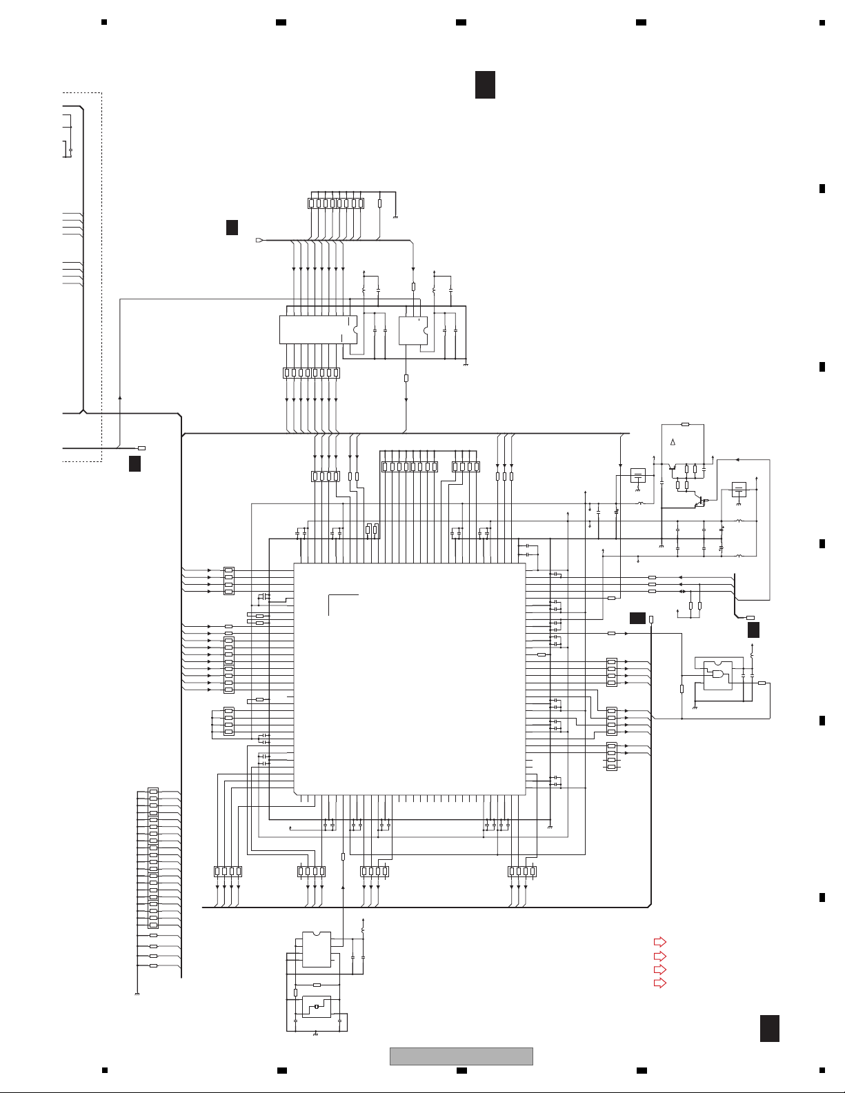
!
PPD0
PPD1
PPD2
PPD3
PPD4
PPD5
PPD6
PPD7
PPD8
PPD9
ADV0
ADV1
ADV2
ADV3
ADV4
ADV5
ADV6
ADV7
ADV8
ADV9
ADV10
ADV11
ADV12
ADV13
ADV14
ADV15
ADV16
ADV17
ADV18
ADV19
VDECOCLK
VDECOCLK
PPDE
PPVSYNC
PPHSYNC
XABT_RST
ADV8
ADV9
ADV10
ADV11
ADV12
ADV13
ADV14
ADV15
ADV17
ADV19
ADV16
ADV18
JPGDT3
JPGDT2
JPGDT1
JPGDT3
JPGDT5
JPGDT4
JPGDT0
VDECOCLK
JPGDT2
JPGDT6
JPGDT1
JPGDT7
JPGDT0
JPGCLK
XNWJPG_SEL
JPGDT7
JPGDT6
JPGDT5
JPGCLK
JPGDT4
ADV19
ADV18
ADV17
ADV16
ADV15
ADV14
ADV13
ADV12ADV 12
ADV13
ADV14
ADV15
VDECDE
VDECHSYNC
VDECVSYNC
ADV11
ADV10
VDECDE
VDECHSYNC
VDECVSYNC
ABT_3V_ON
ADV9
ADV8
ADV7
ADV6
ADV5
ADV4
ADV3
ADV2
ADV1
ADV0
PPD12
PPD13
PPD14
PPD15
PPD10
PPD11
PPD16
PPD17
PPD18
PPD19
VSDA
VSCL
PPICLK
ACH7337-1
C1269
100u/16
ACH7354-1
C1271
220u/6.3
ACH7354-1
C1273
220u/6.3
C1274
NM
(2125)
10u/10
C1272
DCH1201-A
(2125)
10u/10
C1270
DCH1201-A
(2125)
10u/10
C1268
330p/50
C1267
0.1u/16
C1265
0.1u/16
C1264
330p/50
C1263
0.1u/16
C1262
330p/50
C1261
0.1u/16
C1260
330p/50
C1259
0.1u/16
C1258
330p/50
C1257
0.1u/16
C1256
330p/50
C1255
0.1u/16
C1254
330p/50
C1253
0.1u/16
C1252
330p/50
C1250
0.1u/16
C1249
330p/50
C1248
0.1u/16
C1247
330p/50
C1246
0.1u/16
C1245
330p/50
C1244
0.1u/16
C1243
100p/50
C1242
0.1u/16
C1241
330p/50
C1240
0.1u/16
C1239
330p/50
C1238
1u/10
C1237
100p/50
C1236
0.1u/16
C1235
10p/50
C1234
1u/10
C1266
330p/50
C1231
330p/50
C1230
0.1u/16
*C1317
7p/50
CH
C1232
0.1u/16
C1275
0.01u/16
C1332
10p/50
C1333
0.1u/16
C1331
470p/50
C1334
470p/50
C1330
0.1u/16
C1329
NM
C1202
10p/50
CH
C1201
10p/50
CH
C1203
0.1u/16
C1204
470p/50
C1336
NM
C1233
330p/50
C1335
NM
C1338NMC1337
NM
C1340
NM
(3216)
22u/10
C1339
ACG1150-A
(3216)
22u/10
F1202
NM
3
2
1
F1201
NM
3
2
1
GNDD
GNDD
GNDD
GNDD
GNDD
GNDD
GNDD
GNDD
GNDD
IC1206
NM
1
2
GND
34
5
VCC
IC1205
TC7SZ125FU
G
1IN2
GND
3
OUT
4
5
VCC
TC7WHU04FK
IC1201
1A
1
3Y
2
2A
3
GND
45
2Y
6
3A
7
1Y
8
VCC
IC1204
TC74LCX541FK
OE1
1A12
A23A3
4
5
A46A57A68A79A8
10
GND
11
Y812Y713Y614Y515Y416Y317Y2
18Y119
OE2
20
VCC
ABT1015
IC1203
RED(0)1RED(1)2RED(2)3RED(3)4PLL_VSS15PLL_VDD1
6
SYSCLK7IO_VDD18IO_VSS19RED(9)10RED(10)11CORE_VDD112CORE_VSS113RED(11)14BLUE(0)15BLUE(1)16BLUE(2)17BLUE(3)
18
BLUE(4)19BLUE(5)
20
BLUE(6)
21
BLUE(7)22BLUE(8)23BLUE(9)24BLUE(10)25BLUE(11)26CORE_VDD227CORE_VSS2
28
IO_VDD2
29
IO_VSS2
30
HSN
31
VSN
32
IO_VDD3
33
IO_VSS3
34
DE
35
GREEN(0)
36
GREEN(1)
37
GREEN(2)
38
GREEN(3)
39
GREEN(4)
40
CORE_VDD3
41
CORE_VSS3
42
GREEN(5)
43
IO_VDD4
44
IO_VSS4
45
GREEN(6)
46
GREEN(7)
47
GREEN(8)
48
GREEN(9)
49
GREEN(10)
50
GREEN(11)
51
INVOUTCLK
52
CORE_VDD4
53
CORE_VSS4
54
VOUTCLK
55
PLL_VSS2
56
PLL_VDD2
57
IO_VDD5
58
IO_VSS5
59
INPUTVCLK
60
SDA
61
SCL
62
RESETN
63
CORE_VDD5
64
CORE_VSS5
65
INPUTDE
66
INPUTHSN
67
INPUTVS N
68
CORE_VDD669CORE_VSS6
70
INPUTCB(0)71INPUTCB(1)
72
IO_VDD673IO_VSS6
74
INPUTCB(2)
75
INPUTCB(3)76INPUTCB(4)
77
INPUTCB(5)78INPUTCB(6)79INPUTCB(7)80INPUTCB(8)81INPUTCB(9)
82
INPUTCB(10)83INPUTCB(11)
84
INPUTY(0)
85
INPUTY(1)86INPUTY(2)87INPUTY(3)88INPUTY(4)
89
IO_VDD7
90
IO_VSS7
91
INPUTY(5)
92
INPUTY(6)
93
INPUTY(7)
94
CORE_VDD795CORE_VSS7
96
INPUTY(8)
97
INPUTY(9)
98
INPUTY(10)
99
INPUTY(11)
100
IO_VSS8
101
IO_VDD8
102
INPUTCR(0)
103
INPUTCR(1)
104
INPUTCR(2)
105
INPUTCR(3)
106
INPUTCR(4)
107
INPUTCR(5)
108
INPUTCR(6)
109
INPUTCR(7)
110
INPUTCR(8)
111
INPUTCR(9)
112
INPUTCR(10)
113
INPUTCR(11)
114
IRQ_N
115
TRSTN
116
TCK
117
TDO
118
TDI
119
TMS
120
IO_VDD9
121
RED(4)
122
CORE_VDD8
123
CORE_VSS8
124
RED(5)
125
RED(6)
126
RED(7)
127
RED(8)
128
L1208
VTL1129-A
L1216
VTL1129-A
L1210
ATF1211-A
(1608)
L1218
NM
L1209
ATF1211-A
(1608)
L1217
VTL1129-A
L1201
VTL1129-A
NM
Q1208
NM
Q1207
R1292
47
2
1
4
3
6
5
8
7
R1309
68
214
3
658
7
R1241
47k
2
1
4
3
6
5
8
7
R1303
47k
2
1
4
3
658
7
R1242
47k
2
1
4
3
6
5
8
7
R1243
47k
2
1
4
3
6
5
8
7
R1244
47k
2
1
4
3
6
5
8
7
R1290
47
214
3
658
7
R1310
68
214
3
658
7
R1291
47
214
3
658
7
R1251
4.7k
2
1
4
3
6
5
8
7
R1261
4.7k
2
1
4
3
658
7
R1245
47k
2
1
4
3
6
5
8
7
R1293
47
2
1
4
3
6
5
8
7
R1268
33
2
1
4
3
6
5
8
7
R1205
33
2
1
4
3
6
5
8
7
R1204
4.7k
214
3
658
7
R1266
33
214
3
658
7
R1203
33
2
1
4
3
6
5
8
7
R1294
47
2
1
4
3
6
5
8
7
R1305
47k
214
3
658
7
R1264
4.7k
214
3
658
7
R1295
47
214
3
658
7
R1289
47
214
3
658
7
R1249
47
R1250
4.7k
R1202
1M
R1252
10
R1218
4.7k
R1207
4.7k
R1206
4.7k
R1253
10
R1300
47k
R1299
47k
R1297
33
R1260
47
R1259
47
R1258
47
R1257
33
R1256
33
R1248
4.7k
R1247
100
R1304
47k
R1308
68
R1302
0
R1246
47k
R1314NMR1313
NM
R1312
NM
R1311
NM
R1296
47
R1201
1.5k
R1317
2.2k
R1318
2.2k
R1322
NM
R1255
470
R1208
4.7k
R1319
0
(2125)
R1323
0
R1298
33
R1301
47k
V+3R3_HHH
V+3R3_ABT
V+3R3_ABT
V+3R3_HHH
V+3R3_AB
V+3R3_AB
V+1R8_ABT
V+1R8_HHH
V+3R3_ABT
V+3R3_HHH
V+1R8_ABTPLL
V+1R8_ABTPLL
X1201
ASS7106-1
FA-238 27MHz CL=7pF
1
1
GND1
2
GND2
4
3
3
NWJPG
CONT_SUB
DV_TX
CONT_SUB
97
98
99
100
D
3/7
D-MAIN ASSY (7028071691050-IL)
D
3/7
D 2/7
D 1/7,2/7
D 1/7,2/7
D 6/7
: Video Signal Route (Y)
(Y)
: Video Signal Route (Cb)
(Cb)
: Video Signal Route (Cr)
(Cr)
: Video Signal Route (TV/SAT)
5
6 7 8
A
B
5
VSX-1022-K
6 7 8
C
D
E
F
95

1
ADDATO
DIRDATO
D1BCK
D1LRCK
DIRLRCK
DIRBCK
DIRMCKO
4588_SDA
4588_SCL
4588_PDN
MSPDIF
232RX
232TX
D1FDT
D1CDT
D1SDT
D1BWDT
AKM7115-1
CN 1402
20010WS-08
232RX
1
232TX
2
V+5_HD
3
GNDD
4
COAX IN
5
GNDD
6
V+3R3
7
OPT IN
8
CN 1401
AKN7071-A
C125Z2-19
SBLO
1
GNDDAC
2
SBRO
3
GNDDAC
4
SWO
5
GNDDAC
6
CO
7
GNDDAC
8
SLO
9
GNDDAC
10
SRO
11
GNDDAC
12
GNDDAC
14
FRO
15
GNDA
16
LIN
17
GND VCOMDAC
18
RIN
19
FLO
13
NM
C1434
ACH7354-1
C1457
220u/6.3
ACH7354-1
C1402
220u/6.3
ACH7354-1
C1415
220u/6.3
ACH7354-1
C1420
220u/6.3
ACH7328-1
C1429
4.7u/35
C1409
4.7u/16
(2125)
C1426
0.1u/16
C1410 0.1u/16
C1477
NM
C1476
NM
C1475
18p/50
C1411 470p/50
C1427
470p/50
C1462NMC1461
NM
C1442
0.1u/16
C1459
100p/50
C1458
0.1u/16
C1456
330p/50
C1450
470p/50
C1449
470p/50
C1474
330p/50
C1446
470p/50
C1445
470p/50
C1473
0.1u/16
C1443
470p/50
C1431
2.2u/16
(2125)
C1430
0.1u/16
C1425
0.1u/16
C1428
330p/50
C1421
0.1u/16
C1422
470p/50
C1423
0.01u/16
C1424
10p/50
C1418
0.01u/16
C1419
330p/50
C1417
470p/50
C1416
0.1u/16
C1406NMC1405
0.01u/16
C1404
470p/50
C1403
0.1u/16
C1478
0.01u/25
C1479
NM
(1608)
C1480
NM
(1608)
C1481
2200p/50
(1608)
C1433
100p/50
C1432
100p/50
C1401
470p/50
C1460
0.01u/25
C1447
470p/50
C1448
470p/50
C1482
330p/50
C1452
47p/50
C1444
470p/50
C1437NMC1436
NM
C1435
NM
C1451
1u/10
D1402
DAP202U
D1406
DAN217U
D1405
DAN217U
D1401
DAN202U
GN DD
GN DD
GN DD
GN DD
GN DD
GN DD
GN DDAC
GN DDAC
GN DDAC
GN DD
GN DDACP
GN DDAC
GN DDGN DDACP
GN DDACP
GN DDAC
GN DD
GN DDACP
GN DD
IC1402
TC74VHC08 FK
(2/4)
6
4
5
14
7
IC1402
TC74VHC08 FK
(1/4)
3
1
2
14
7
IC1402
TC74VHC08 FK
(3/4)
8
9
10
14
7
IC1402
TC74VHC08 FK
(4/4)
11
12
13
14
7
IC1403
74VHCU04MTCX
1A11Y
2
2A32Y
4
5
3A63Y7GND
84Y94A105Y115A12
6Y136A
14
VCC
AK4588VQ
IC1401
INT1
1
BOUT
2
TVDD
3
DVDD
4
DVSS
5
XTO
6
XTI
7
TEST3
8
MCKO2
9
MCKO1
10
COUT
11
UOUT
12
VOUT
13
SDTO2
14
BICK2
15
LRCK2
16
SDTO1
17
BICK1
18
LRCK1
19
CDTO
20
CCLK/SCL21CDTI/SDA
22
CSN
23
DAUX124SDTI425SDTI3
26
SDTI2
27
SDTI1
28
XTL129XTL0
30
PDN
31
MASTER
32
DZF2/OVF
33
DZF1
34
LOUT4
35
NC_1
36
ROUT4
37
NC_2
38
LOUT3
39
NC_3
40
ROUT3
41
NC_4
42
LOUT2
43
NC_5
44
ROUT2
45
NC_6
46
LOUT1
47
NC_7
48
ROUT1
49
NC_8
50
LIN
51
RIN
52
VCOM
53
VREFH
54
AVDD
55
AVSS
56
RX0
57
NC_9
58
RX1
59
TEST1
60
RX261NC_1062RX363PVSS64R65PVDD
66
RX467TEST268RX569CAD070RX671CAD172RX773I2C74DAUX275VIN76MCLK77TX078TX179INT0
80
L1403
VTL1129-A
L1404
VTL1129-A
L1408
VTL1129-A
L1406
VTL1129-A
L1402
L1405
VTL1129-A
R1479
10k
R1480
NM
R1495
NM
R1433
NM
(2125)
R1494
0
R1492
NM
(1608)
R1493
NM
(1608)
R1449
47
R1507
2.2k
R1505
33
R1487
150
R1488
150
R1504
33
R1438
100
R1427
NM
(2125)
R1451
100
R1412
100
R1425
10
R1478
10k
R1409
0
R1408
NM
R1407
0
R1410
0
R1406
NM
R1405
NM
(1608)
R1404
NM
(1608)
R1424
0
R1403
100
R1402
100
R1422
NM
R1421
NM
R1477
4.7k
R1470
47k
R1455
100
R1462
33
R1461
33
R1476
4.7k
R1452
220
R1454
NM
R1429
10k
R1447
100
R1434
12k
(D)
R1446
100
R1450
150
R1445
100
R1444
100
R1443
100
R1432
NM
(2125)
R1426
2.2
R1442
100
R1413
0
R1441
100
R1436
100
R1509
10k
R1415
0
R1498
0
R1497
0
R1496
0
R1448
100
R1440
100
R1506
47k
R1512
0
R1511
0
R1499
0
R1508
47
R1475
4.7k
R1513
0
R1503
0
R15020R1501
0
R1500
0
R1474
4.7k
R1458
0
R1453
0
R1420
NM
R1414
NM
R1473
0
R1464
47
R1401
47k
R1459
33
R1460
33
R1457
33
R1456
33
R1439
100
R1419
NM
R1418
100
R1417
47k
R1416
2.2k
R1423
100
R1411
0
V+5_HD
V+5_DACD
V+5_HD
V+5_HD
V+5_DACA
V+3R3_DSP
V+3R3_DSP
V+3R3_DSP_TVDD
V+3R3_DAUDIO
V+5_HD
V+3R3_DSP_TVDD
V+5_DACA
V+3R3_DSP
V+3R3_DSP
X1401
ASS7105-1
SG-310SCN 24.576MHz
ST
1
GND
2
VCC
4
OUT
3
CONT_MAIN
DIRMCK
NETSPDIF
DAMCLK
ARCSPDIF
D1MCLK
DSP
232DEBUG
XMCK
DAMCLK
DSPMCLKI
DIRMCKI
MASTER CLOCK SELECTOR
(C)
(SW)
VTL1129-A
D
4/7
M
CP2003
L
CN2009
D 1/7
D 2/7,5/7
D 5/7
D 2/7
D 6/7
D 1/7,2/7,3/7,5/7,7/7
(FL)
(SL)
(C)
(SW)
(SBL)
(FL)
(SL)
(C)
(SW)
(SBL)
2 3 4
10.10 D-MAIN ASSY (4/7)(VSX-1022-K, VSX-42)
A
B
C
D
E
F
96
VSX-1022-K
1
2 3 4

5
P1MCLK
DSPLRCK
DSPBCK
D1MCLK
CDTI/DSDFR
HDMI_SEL
DSD_SEL
DIRLRCK
DIRMCKO
DIRBCK
ADDATO
DIRDATO
D1BCK
D1LRCK
DIRLRCK
DIRBCK
DIRMCKO
P1BCK
HDMI_BCK'
P1_LRCK/DSDFR
P1_CDTI
NM
C1441
NM
C1414
ACH7354-1
220u/6.3
C1470
10p/50
C1469
NM
C1439 0.1u/16
C1440 470p/50
C1418
0.01u/16
C1419
330p/50
C1412
NM
C1407 0.1u/16
C1413
10p/50
C1408 470p/50
D1405
DAN217U
GN DD
GN DD
GN DD
GN DD
GN DD
GN DDAC
GN DDDDACP
GN DDAC
TC74VHC157FK
IC1406
SELECTOR
SELECT
1
1A
2
1B
3
1Y
4
5
2A
6
2B
7
2Y
8
GND
DATA
9
3Y
10
3B
11
3A
LRCK
12
4Y
13
4B
14
4A
15
XST
16
VCC
TC74VHC157FK
IC1405
SELECTOR
SELECT
1
1A
2
1B
3
MCK
1Y
4
5
2A
6
2B
BCK
7
2Y
8
GND
FD
9
3Y
10
3B
11
3A
LRCK
12
4Y
13
4B
14
4A
15
XST
16
VCC
KN1401
ANE7368 -1
4010-210190-610-0S(INKEL)
GND1
1
GND2
2
GND3
3
GND4
4
L1403
VTL1129-A
L1401
VTL1129-A
L1409
VTL1129-A
L1406
VTL1129-A
R1482100
R148610
R1491 47
R1425
10
R1405
NM
(1608)
R1404
NM
(1608)
R1472 NM
R1484100
R148347
R1471 47k
R1430 100
R1467 47k
R1431 47
R1435 47
R1468 47k
R1469 47k
R14810
R1432
NM
(2125)
R1489
NM
R1466
NM
R1465
NM
R1463
NM
R1458
0
R1453
0
R1420
NM
R1414
NM
R1428 100
R1485100
R1437 100
R1490 100
R1510
47k
V+5_HD
V+5_DACD
V+3R3_DSP
V+3R3_DSP
V+3R3_DSP_TVDD
CONT_MAIN
CONT_MAIN
DIRMCKI
DSP
FL/FR
HDMI PCM DATA HDMI DSD DATA
SBL/SBR
SL/SR
C/SW HDLRCK
FL
BDTI
CDTI
HFDT
SDTI
HFDT
FR
A CODEC
B HDMI
A HD AUDIO
B DSD
D
4/7
D-MAIN ASSY (7028071691050-IL)
D
4/7
D 1/7,2/7,3/7,5/7,7/7
(FL)
: Audio Signal Route (Front L ch)
(SL)
: Audio Signal Route (Surround L ch)
(C)
: Audio Signal Route (Center ch)
(SW)
: Audio Signal Route (SubWoofer ch)
(SBL)
: Audio Signal Route (Surround Back L ch)
: Audio Signal Route (L ch)
6 7 8
A
B
C
D
E
F
VSX-1022-K
5
6 7 8
97

1
EM_A10
EM_A0
EM_A1
EM_A2
EM_A3
EM_A4
EM_A5
EM_A6
EM A7
A10
A0
EM_/OE2
EM_/RW2
EM_/CS2
EM_/RAS
SDRAM_/CS
EM_/BA0
EM_/BA1
DSP_SCL
DSP_CS
A10
A0A1A2A3A4A5A6
A7
A7
A6
A5
A4A3A2
A1
TDO
TDI
TMS
/TRST
EM_A17
EM_A18
EM_A12
EM_A13
EM_A14
EM_A15
EM_A16
DSP_SDA
DSP_RST
D1CDT
D1SDT
D1BWDT
DIRDATO
ADDATO
DSPMCLKI
D1LRCK
D1BCK
P1_BDTI
P1_SDTI
CDTI/DSDFR
P1_HFDT/DSDFL
DSPLRCK
DSPBCK
DSP_RDY
HDMI_BCK'
DSP_SDOUT
D1BCK
D1LRCK
D1FDT
ACH7354-1
C1615
220u/6.3
ACH7354-1
C1601
220u/6.3
ACH7354-1
C1616
220u/6.3
C1657
NM
C1652
NM
C1655
0.01u/25
C1651
0.1u/16
C1650NMC1649
0.1u/16
C1605
0.1u/16
C1604
330p/50
C1613
0.1u/16
C1612
0.1u/16
C1611
100p/50
C1610
0.1u/16
C1603
330p/50
C1602
100p/50
C1609
0.1u/16
C1607
0.1u/16
C1606
NM
C1660
NM
C1639
NM
C1659
NM
C1664NMC1663
NM
C1661NMC1654
NM
C1665
330p/50
C1624
330p/50
C1623
4700p/50
C1622
330p/50
C1621
0.01u/25
C1620
100p/50
C1619
0.01u/25
C1618
0.01u/25
C1627
0.1u/16
C1626
0.1u/16
C1667
NM
C1666
NM
C1614
0.01u/25
C1632
0.01u/25
C1608
330p/50
C1631
330p/50
C1630
33p/50
C1658
NM
C1653
0.01u/25
C1617
330p/50
C1628
100p/50
C1629
100p/50
C1669
100p/50
C1645
330p/50
C1648
0.1u/16
C1647
0.1u/16
C1635
100p/50
C1634
100p/50
C1668
NM
C1672
DCH1201-A
(2125)
10u/10
C1673
NM
(2125)
C1662
0.1u/16
TMS320DA788B
IC1601
VSS11AHCLKX0
2
AMUTE0
3
AMUTE14AHCLKX15VSS26ACLKX1
7
CVDD18ACLKR1
9
DVDD110AFSX111AFSR112VSS313RESET
14
VSS415CVDD2
16
CLKIN
17
VSS518TMS19CVDD320TRST
21
OSCVSS
22
OSCIN23OSCOUT24OSCVDD25VSS626PLLHV27TDI
28
TDO
29
30 79
EM_A[6]
80
DVDD881VSS16
82
EM_A[5]83EM_A[4]
84
CVDD10
85
EM_A[3]
86
VSS17
87
EM_A[2]88EM_A[1]
89
CVDD11
90
EM_A[0]
91
DVDD9
92
EM_A[10]93EM_BA[1]
94
VSS18
95
EM_BA[0]96EM_CS[0]
97
EM_RAS
98
VSS19
99
EM_CS[2]
100
CVDD12
101
EM_RW
102
DVDD10
103
EM_OE
104
SPI0_ENA
105
VSS20
106
SPI0_SCS
107
SPI0_CLK
108
VSS21
109
SPI0_SIMO
110
SPI0_SOMI
111
DVDD11
112
AXR0[0]
113
VSS22
114
AXR0[1]
115
AXR0[2]
116
AXR0[3]
117
VSS23
118
AXR0[4]
119
AXR0[5]
120
AXR0[6]
121
AXR0[7]
122
CVDD13
123
VSS24
124
DVDD12
125
AXR0[8]
126
AXR0[9]
127
CVDD14
128
VSS25
129
AXR0[10]
130
AXR0[11]
131
CVDD15
132
VSS26
133
AXR0[12]
134
AXR0[13]
135
DVDD13
136
AXR0[14]
137
AXR0[15]
138
ACLKR0
139
VSS27
140
AFSR0
141
ACLKX0
142
AHCLKR0
143
AFSX0
144
L1604
ATF1211-A
(1608)
L1602
ATF1211-A
(1608)
L1601
ATF1211-A
(1608)
R1707
33
214
3
6
5
8
7
R1708
33
2
1
4
3
6
5
8
7
R1709
1k
2
1
4
3
658
7
R1705
2
1
8
7
R1706
33
214
3
6
5
8
7
R1651
NM
R1649
33
R1646
33
R1647
1k
R1627
33
R1625
33
R1624
4.7k
R1677
47
R1693
NM
R1688
1k
R1686
33
R1673
0
R1605
33
R1604
33
R1603
33
R1619
33
R1618
33
R160233R1601
33
R161733R1616
33
R1676
0
R1684
33
R1661
0
R1662
0
R1672
47k
R1671
NM
R1689
1k
R1692
2.7k
R1685
10k
R167933R1680
33
R1615
4.7k
R1667
33
R1664
33
R1659
0
R1658
0
R1695
0
R1696
0
R1654
0
R1655
0
R1687
33
V+3R3_DSP
V+1R2_HHH
V+3R3_HHH
V+3R3_DSP
V+3R3_DSP
V+1R2_DSP
CONT_MAIN
XMCK
DSP
8
162033445357657785
90
101
123
128
132
25
8150921073
314260
112
68
125
136
103
D
5/7
D 2/7,4/7
D 1/7,2/7,3/7,4/7,7/7
D 4/7
2 3 4
10.11 D-MAIN ASSY (5/7)(VSX-1022-K, VSX-42)
A
B
C
D
E
F
98
1
VSX-1022-K
2 3 4

EM_A0
EM_A1
EM_A2
EM_A3
EM_A4
EM_A5
EM_A6
EM_A7
EM_A8
EM_A9
EM_A11
A0
A11
A0A1A2A3A4A5A6A7A8
A9
A11
A9A8A7
A6
A5
A4A3A2
A1
EM_A3
EM_A2
EM_A1
EM_A0
EM_A10
EM_/BA1
EM_/BA0
SDRAM_/CS
EM_/RAS
EM_/CAS1
EM_/WE1
EM_/LDQM
EM_D14
EM_D13
EM_D12
EM_D11
EM_D10
EM_D9
EM_D8
EM_A4
EM_A5
EM_A6
EM_A7
EM_A8
EM_A9
EM_A11
EM_CKE2
EM_CLK2
EM_/UDQM
EM_D15
EM_A15
EM_/BA0
EM_/BA1
EM_/CS2
A0
A1
EM_A2
EM_A3
EM_A4
EM_A5
A6
EM_A16
EM_A17
EM_/WE2
EM_A18
A7
A8
A9
A10
A11
EM_A12
EM_A13
EM_A14
EM_D3
EM_/OE2
EM_D0
EM_D1
EM_D2
EM_D4
EM_D5
EM_D6
EM_D7
EM_/RW2
EM_/CAS1
EM_/WE2
EM_/WE1
EM_/LDQM
EM_CKE2
EM_/UDQM
EM_D8
EM_D9
EM_D10
EM_D11
EM_D12
EM_D13
EM_D0
EM_D1
EM_D4
EM_D5
TCK
/EMU1
/EMU0
TDO
TDI
TMS
/TRST
EM_CLK2
TDO
TCK
TDI
/TRST
TMS
/EMU0
/EMU1
DSP_RST
EM_D15
EM_D14
EM_D3
EM_D2
EM_D7
EM_D6
EM_D6
EM_D5
EM_D7
EM_D4
EM_D0
EM_D1
EM_D2
EM_D3
NM
CN1601
DUMMY
TMS
1
/RST
2
TDI
3
GNDD
4
V+3R3V
5
GNDD
6
TDO
7
TCK
8
/EMU0
9
/EMU1
10
ACH7354-1
C1671
220u/6.3
ACH7354-1
C1643
220u/6.3
C1670
0.01u/25
C1646
0.1u/16
C1644
0.01u/25
C1656
NM
C1636
330p/50
C1638
0.22u/6.3
C1642
0.22u/6.3
C1640
0.1u/16
C1637
33p/50
C1633
100p/50
C1645
330p/50
C1625
0.22u/6.3
C1648
0.1u/16
C1641
10p/50
C1668
NM
C1672
DCH1201-A
(2125)
10u/10
GNDD
GNDD
GNDD
IC1603
MX29LV160DTTI-70G
A15
1
A14
2
A13
3
A12
4
5
A11
6
A10
7
A9
8
A8
9
A19
10
NC1
11
WE#
12
RESET#
13
NC2
14
WP#
15
RY/BY#
16
A18
17
A17
18
A7
19
A6
20
A5
21
A4
22
A3
23
A2
24
A1
25
A0
26
CE#
27
VSS1
28
OE#
29
DQ0
30
DQ8
31
DQ1
32
DQ9
33
DQ2
34
DQ10
35
DQ3
36
DQ11
37
VCC
38
DQ4
39
DQ12
40
DQ5
41
DQ13
42
DQ6
43
DQ14
44
DQ7
45
DQ15_A-1
46
VSS2
47
BYTE#
48
A16
IC1602
W98 64G6JH-6
VDD1
1
DQ0
2
VDDQ1
3
DQ1
4
5
DQ2
6
VSSQ1
7
DQ3
8
DQ4
9
VDDQ2
10
DQ5
11
DQ6
12
VSSQ2
13
DQ7
14
VDD2
15
LDQM
16
WE
17
CAS
18
RAS
19
CS
20
BS0
21
BS1
22
A10/AP
23
A0
24
A1
25
A2
26
A3
27
VDD328VSS1
29
A4
30
A5
31
A6
32
A7
33
A8
34
A9
35
A11
36
NC1
37
CKE
38
CLK
39
UDQM
40
NC2
41
VSS2
42
DQ8
43
VDDQ3
44
DQ9
45
DQ10
46
VSSQ3
47
DQ11
48
DQ12
49
VDDQ4
50
DQ13
51
DQ14
52
VSSQ4
53
DQ15
54
VSS3
VSS518TMS19CVDD320TRST
21
OSCVSS
22
OSCIN23OSCOUT24OSCVDD25VSS626PLLHV27TDI
28
TDO29VSS730DVDD231EMU[0]
32
CVDD433EMU[1]
34
TCK35VSS8
36
EM_CAS
37
EM_WE
38
EM_WE_DQM[0]
39
VSS9
40
EM_D[7]
41
DVDD3
42
EM_D[6]
43
CVDD5
44
EM_D[5]
45
EM_D[4]
46
VSS10
47
EM_D[3]
48
EM_D[2]
49
DVDD4
50
EM_D[1]
51
EM_D[0]
52
CVDD6
53
VSS11
54
EM_D[15]
55
EM_D[14]
56
CVDD7
57
EM_D[13]
58
EM_D[12]
59
DVDD5
60
EM_D[11]
61
VSS12
62
EM_D[10]
63
EM_D[9]
64
CVDD8
65
EM_D[8]
66
EM_WE_DQM[1]
67
DVDD6
68
VSS13
69
EM_CLK
70
EM_CKE
71
VSS14
72
DVDD7
73
EM_A[11]
74
EM_A[9]75EM_A[8]
76
CVDD9
77
VSS15
78
EM_A[7]79EM_A[6]
80
DVDD881VSS16
82
EM_A[5]83EM_A[4]
84
CVDD10
85
EM_A[3]
86
VSS17
87
EM_A[2]88EM_A[1]
89
CVDD11
90
EM_A[0]
91
L1604
ATF1211-A
(1608)
L1603
ATF1211-A
(1608)
R1704
33
2
1
4
3
6
5
8
7
R1703
33
2
1
4
3
6
5
8
7
R1702
33
2
1
4
3
6
5
8
7
R1701
33
2
1
4
3
6
5
8
7
R1698
68
2
1
4
3
6
5
8
7
R1697
68
2
1
4
3
6
5
8
7
R1705
33
214
3
6
5
8
7
R1706
33
214
3
6
5
8
7
R1665
33
R1669
33
R1690
10k
R1691
10k
R1668
33
R1666
33
R1686
33
R1630
33
R1628
33
R1626
33
R1670
33
R1675
0
R1674
NM
R1678
10k
R1614
33
R1673
0
R1605
33
R1604
330
R1694
0
(2125)
R1685
10k
R167933R168033R1681
33
R1682
33
R1683
33
R1687
33
V+3R3_DSP
V+3R3_DSP
V+3R3_DSP
NOR_FLASH 16Mb
SDRAM 64Mb
D
5/7
D-MAIN ASSY (7028071691050-IL)
D
5/7
D 4/7
5
6 7 8
A
B
6 7 8
5
VSX-1022-K
C
D
E
F
99
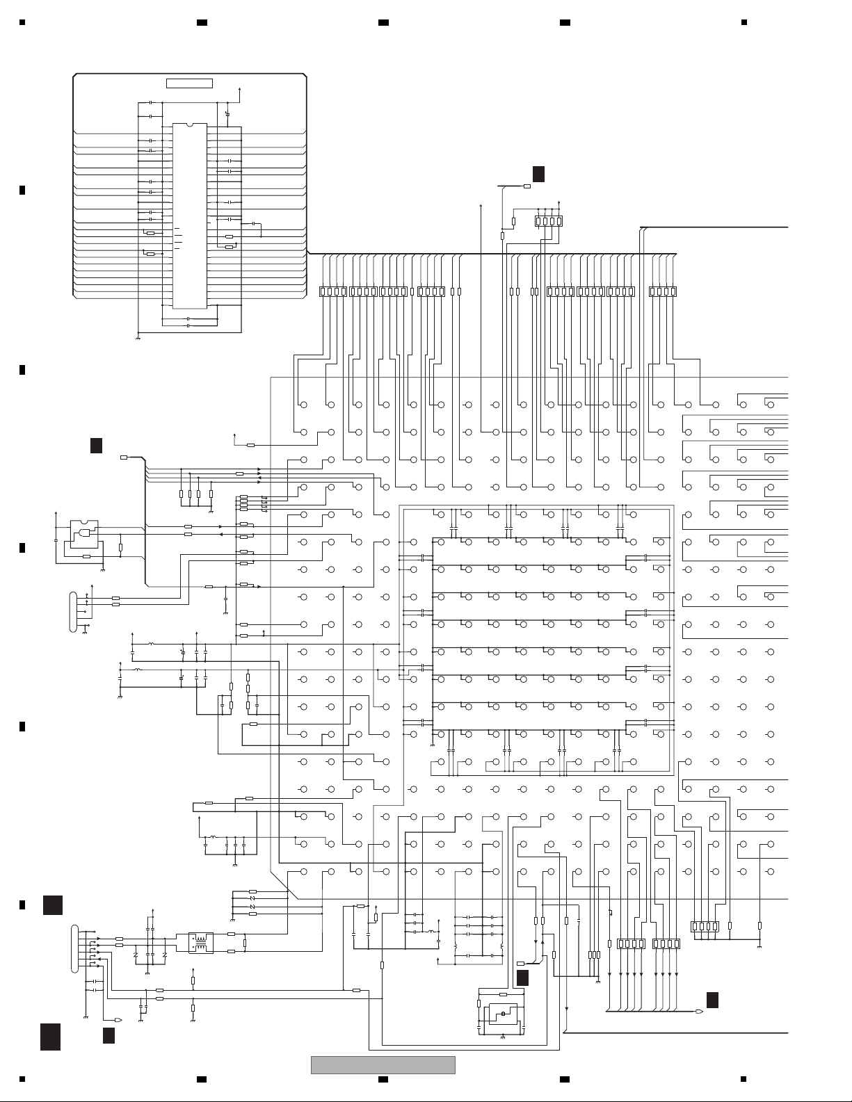
1
NWSA4
NWSCS
NWSA12
NWSDQ6
NWSDQ9
NWSDQ15
NWSDQ13
NWSA5
NWSDQM0
NWSA6
NWSDQM1
NWSDQ2
NWSA7
NWSDQ11
NWSBA1
NWSDQ10
NWSA8
NWSA6NWSA1
NWSDQ9
NWSCAS
NWSRAS
NWSA9
NWSDQ8
NWSCAS
NWSDQM1
NWSA4
NWSCS
NWSDQ14
NWSDQ10
NWSDQ6
NWSCLK
NWSA11
NWSA12
NWSA0
NWSDQ7
NWSA10
NWSDQ12
NWSDQ5
NWSDQ14
NWSDQ2
NWSCKE
NWSA3
NWSDQ15
NWSDQ3
NWSBA0
NWSA2
NWSDQ4
NWSDQ1
NWSA7
NWSDQ0
NWSA3
NWSA5
NWSDQM0
NWSA0
NWSDQ13
NWSA2
NWSDQ12
NWSA10
NWSDQ11
NWSA1
NWSA9
NWSDQ7
NWSA8
NWSRAS
NWSBA1
NWSDQ4
NWSCLK
NWSDQ0
NWSDQ5
NWSWE
NWSDQ3
NWSDQ8
NWSWE
NWSA11
NWSDQ1
NWSCKE
XAPRST
JPGDT4
JPGDT5
JPGDT6
JPGDT7
JPGDT0
JPGCLK
JPGDT1
JPGDT2
JPGDT3
NWSBA0
REQ_NW
DI_NW
BTPOW
XDET_BT
XFUSBERR
XRST_NW
BTTX
CS_NW
DO_NW
CLK_NW
WOL_NW
NWFDQ0
NWFDQ1
BTRX
BTRX2
BSL_NW
AKM7141-1
CN9202
20022WS-06
GNDD
1
D-
2
D+
3
XUSBERR
4
USBPOW
5
USBDDCERR
6
CN9201
VKN1374-A
GND
1
V+3R3
2
NC
3
TXD1
4
RXD1
5
NM
C9314
NM
C9312
ACH7354-1
C9217
220u/6.3
C9235
1000p/50
C9270
0.1u/16
C9236
10u/10
C9308
NM
C9245
18p/50
CH
C9246
22p/50
CH
C9318
NM
C9264
C9207
0.1u/16
C9224
NM
C9324
0.01u/25
C9325
2200p/50
C9260
0.1u/16
C9210
0.1u/16
C9271
1000p/50
C9243
1000p/50
C9313
NM
C9204
100p/50
CH
C9255
1000p/50
C9323
NM
C9322
NM
C9259
100p/50
C9263
C9321
NM
C9320
NM
C9230
DCH1201-A
(2125)
10u/10
C9205
0.1u/16
C9275
100p/50
C9215
1000p/50
C9317
NM
C9267
C9216
0.1u/16
C9225
NM
C9212 0.1u/16
C9273
10p/50
C9272
0.1u/16
C9239
10u/10
C9256
0.1u/16
C9277
100p/50
C9211 100p/50
C9303
NM
C9238
100p/50
C9315
NM
C9269
C9266
C9234
0.1u/16
C9240
0.1u/16
C9279
1000p/50
C9278
0.1u/16
C9242
0.1u/16
C9229
0.1u/16
C9254
0.1u/16
C9244
0.1u/16
C9253
100p/50
C9228
DCH1201-A
(2125)
10u/10
C9226
DCH1201-A
(2125)
10u/10
C9258
0.1u/16
C9307
NM
C9206
1000p/50
C9306
NM
C9262
C9252
0.1u/16
C9203
0.1u/16
C9276
0.1u/16
C9214
330p/50
C9232
1000p/50
C9265
C9223
0.01u/25
C9209
1000p/50
C9213
0.1u/16
C9227
0.1u/16
C9241
10p/50
C9274
0.1u/16
C9237
0.1u/16
C9261
100p/50
C9268
C9233
DCH1201-A
(2125)
10u/10
C9208
0.01u/25
C9309
NM
C9257
100p/50
C9251
330p/50
C9231
0.1u/16
C9247
330p/50
C9248
2200p/50
C9335
NM
C9250
0.01u/25
GNDD
GNDD
GNDD
GNDD GNDD
GNDD
GNDD
GNDD
GNDD
GNDD
GNDD
GNDD
GNDD
GNDD
GNDD
GNDD
IC9204
DM860
A1
USBDN
A2
VDD33_USB1
A3
VSS33_USB1
A4
NC1
A5
NC2
A6
VDD33_1
A7
RFCLKP
A8
RFRXQP
A9
RFRXIP
A10
HIGHZ
A11
SSMD0
A12
SSMD4
A13
SSM_CMD
A14
RXD1
A15
TDO
A16
TDI
A17
A0
A18
A1
B1
USBDP
B2
VDD33_USB2
B3
VSS33_USB2
B4
NC3
B5
NC4
B6
VSS_1
B7
RFCLKN
B8
RFRXQN
B9
RFRXIN
B10
TEST1
B11
SSMD1
B12
SSMD5
B13
TXD1
B14
RXD0
B15
TMS
B16
SPICLK
B17
SPI_NCS1
B18
A2
C1
VSS12_USB
C2
USB_REXT
C3
USB_XTALO
C4
USB_XTALI
C5
NRES12_OUT
C6
VSS_2
C7
RREF
C8
NC5
C9
NC6
C10
SSM_CLK
C11
SSMD2
C12
SSMD6
C13
TXD0
C14
TCK
C15
SPI_NCS0
C16
A3
C17
A4
C18
A5
D1
VDD12_USB
D2
USB_VBUS
D3
USB_ATST
D4
NRES33_OUT
D5
NRES33_REF
D6
NRES12_REF
D7
VDD33_2
D8
VDD12_1
D9
SSM_WP
D10
SSM_CP
D11
SSMD3
D12
SSMD7
D13
NRESET
D14
SPI_DIN
D15
SPI_DOUT
D16
A6
D17
A7
D18
A8
E1
VSS33_RTC
E2
USBID
E3
USB_VBUSDRV
E4
NC7
E6
VDD12_2
E7
VDD12_3
E8
VDD33_3
E9
VDD33_4
E10
VDD12_4
E11
VDD12_5
E12
VDD33_5
E13
VDD33_6
E15
A9
E16
A10
E17
A11
E18
A12
F1
VDD33_RTC
F2
RTC_XIN
F3
VDD33_PLL
F4
NC8
F5
VDD33_7
F6
VSS_3
F7
VSS_4
F8
VSS_5
F9
VSS_6
F10
VSS_7
F11
VSS_8
F12
VSS_9
F13
VSS_10
F14
VDD12_6
F15
A13_RAS
F16
A14_CAS
F17
A15_BA0
F18
A16_BA1
G1
VDD12_DCO
G2
RTC_XOUT
G3
VSS33_PLL
G4
NC9
G5
VDD33_8
G6
VSS_11
G7
VSS_12
G8
VSS_13
G9
VSS_14
G10
VSS_15
G11
VSS_16
G12
VSS_17
G13
VSS_18
G14
VDD12_7
G15
A17_DQM0
G16
A18_DQM1
G17
A19
G18
A20
H1
VSS12_DCO
H2
VSS12_PLL
H3
VDD12_PLL
H4
NC10
H5
VDD12_8
H6
VSS_19
H7
VSS_20
H8
VSS_21
H9
VSS_22
H10
VSS_23
H11
VSS_24
H12
VSS_25
H13
VSS_26
H14
VDD33_9
H15
A21
H16
A22
H17
A23
H18
NCS3
J1
PDOUT1
J2
VCO1
J3
XTALO
J4
NC11
J5
VDD12_9
J6
VSS_27
J7
VSS_28
J8
VSS_29
J9
VSS_30
J10
VSS_31
J11
VSS_32
J12
VSS_33
J13
VSS_34
J14
VDD33_10
J15
NCS0
J16
NCS1
J17
NCS2
J18
MEMCKE
K1
PDOUT0
K2
VCO0
K3
XTALI
K4
AOUT_LP
K5
VDD33_11
K6
VSS_35
K7
VSS_36
K8
VSS_37
K9
VSS_38
K10
VSS_39
K11
VSS_40
K12
VSS_41
K13
VSS_42
K14
VDD12_10
K15
MEMCLK
K16
NWE
K17
NOE
K18
NWAIT
L1
AV0_CLK
L2
AOUT_LN
L3
AOUT_RN
L4
AOUT_RP
L5
VDD33_12
L6
VSS_43
L7
VSS_44
L8
VSS_45
L9
VSS_46
L10
VSS_47
L11
VSS_48
L12
VSS_49
L13
VSS_50
L14
VDD12_11
L15
D3
L16
D2
L17
D1
L18
D0
M1
AV0_CTRL0
M2
AV0_CTRL1
M3
AV0_CTRL2
M4
AV0_DATA3
M5
VDD12_12
M6
VSS_51
M7
VSS_52
M8
VSS_53
M9
VSS_54
M10
VSS_55
M11
VSS_56
M12
VSS_57
M13
VSS_58
M14
VDD33_13
M15
D7
M16
D6
M17
D5
M18
D4
N1
AV0_DATA2
N2
AV0_DATA1
N3
AV0_DATA0
N4
AV1_DATA3
N5
VDD12_13
N6
VSS_59
N7
VSS_60
N8
VSS_61
N9
VSS_62
N10
VSS_63
N11
VSS_64
N12
VSS_65
N13
VSS_66
N14
VDD33_14
N15
D11
N16
D10
N17
D9
N18
D8
P1
AV1_DATA2
P2
AV1_DATA1
P3
AV1_DATA0
P4
AV2_DATA3
P6
VDD33_15
P7
VDD33_16
P8
VDD12_14
P9
VDD12_15
P10
VDD33_17
P11
VDD33_18
P12
VDD12_16
P13
VDD12_17
P15
FD0
P16
FD1
P17
D13
P18
D12
R1
AV2_CLK
R2
AV2_CTRL1
R3
AV2_DATA2
R4
AV3_CLK
R5
AV3_DATA1
R6
LCD_D11
R7
LCD_D7
R8
LCD_D3
R9
LCD_CTRL0
R10
VPP
R11
MII_TXEN
R12
MII_TXCLK
R13
MII_RXER
R14
MII_CRS
R15
FD2
R16
FD3
R17
FD4
R18
D14
T1
AV2_CTRL0
T2
AV2_DATA1
T3
AV3_CTRL1
T4
AV3_DATA0
T5
LCD_D14
T6
LCD_D10
T7
LCD_D6
T8
LCD_D2
T9
LCD_CTRL1
T10
LCD_CLK
T11
MII_TXER
T12
MII_RXCLK
T13
MII_COL
T14
MII_RXDV
T15
FD5
T16
FD6
T17
FD7
T18
D15
U1
AV2_DATA0
U2
AV3_CTRL0
U3
AV4_DATA1
U4
LCD_D16
U5
LCD_D13
U6
LCD_D9
U7
LCD_D5
U8
LCD_D1
U9
LCD_CTRL2
U10
MII_TXD0
U11
MII_TXD2
U12
MII_RXD0
U13
MII_RXD2
U14
MII_MDIO
U15
NFCE0
U16
FCLE
U17
NFWE
U18
NFRB
V1
NC12
V2
AV4_DATA0
V3
LCD_D17
V4
LCD_D15
V5
LCD_D12
V6
LCD_D8
V7
LCD_D4
V8
LCD_D0
V9
LCD_CTRL3
V10
MII_TXD1
V11
MII_TXD3
V12
MII_RXD1
V13
MII_RXD3
V14
MII_MDC
V15
MII_PHYCLK
V16
NFWP
V17
NFRE
V18
FALE
IC9207
NM
1
2
GND
34
5
VCC
IC9201
W98 25G6JH-6
VDD1
1
DQ0
2
VDDQ1
3
DQ1
4
5
DQ2
6
VSSQ1
7
DQ3
8
DQ4
9
VDDQ2
10
DQ5
11
DQ6
12
VSSQ2
13
DQ7
14
VDD2
15
LDQM
16
WE
17
CAS
18
RAS
19
CS
20
BS0
21
BS1
22
A10/AP
23
A0
24
A1
25
A2
26
A3
27
VDD328VSS1
29
A4
30
A5
31
A6
32
A7
33
A8
34
A9
35
A11
36
A12
37
CKE
38
CLK
39
UDQM
40
NC
41
VSS2
42
DQ8
43
VDDQ3
44
DQ9
45
DQ10
46
VSSQ3
47
DQ11
48
DQ12
49
VDDQ4
50
DQ13
51
DQ14
52
VSSQ4
53
DQ15
54
VSS3
L9217
CTF1703-A
DLP11SN121SL2L
1
1
2
2
3
3
4
4
L9210
VTL1129-A
L9206
ATF1211-A
(1608)
L9209
VTL1129-A
L9207
VTL1129-A
L9208
L9205
ATF1211-A
(1608)
R9227
4.7k
214
3
658
7
R9268
47k
214
3
658
7
R9237
120
214
3
658
7
R9232
47
214
3
658
7
R9233
47
214
3
658
7
R9266
47
214
3
658
7
R9226
47
214
3
658
7
R9234
120
214
3
658
7
R9240
47
2
1
4
3
6
587
R9236
120
214
3
658
7
R9265
47
214
3
6
587
R9235
120
214
3
658
7
R9320
10k
R9269
1.5k
R9337
NM
R9319
10k
R9349
0
R9245
47
R9256
47k
R9279
2.7k
R9326
4.7k
R9255
47k
R9288
100
R9287
100
R9302
10k
R9347
10k
R9239
47
R9247
47
R9243
47
R9305
NM
R9303
10k
R9312
3k
(F)
R9346
10
R9304
10k
R9306
10k
R9253
10k
R9270
10k
R9244
47
R9251
10k
R9359
1M
R9248
10k
R9278
1.5k
R9272
10k
R9241
47
R9238
47
R9217
0
R9220
47
R9358
2.2k
R9246
10k
R9341
0
R9340
0
R9343
NM
R9252
470
R9274
47
R9258
10k
R9339
NM
R9254
10k
R9275
47k
R9276
47k
R9264
47
R9230
NM
R9262
NM
R9261
47
R9348
47k
R9242
47
R9228
4.7k
R9321
10k
R9229
4.7k
R9273
47k
R9363
10k
R9362
10
R9361
0
R9360
NM
R9250
10k
R9345
10
R9318
10
R9317
10
R9338
1k
R9271
13k
R9295
3.3
R9296
3.3
R9249
10k
VA9202
ASQS12U020R2
VA9204
ASQS12U020R2
VA9203
ASQS12U020R2
VA9201
ASQS12U020R2
V+3R3_NWVDD
V+3R3_NWVDD
V+3R3_NW
V+3R3_NWVDD
V+3R3_NW
V+3R3_NWVDD
V+3R3_NWVDD
V+1R2_NW
V+3R3_NWVDD
V+3R3_NWVDD
V+3R3_NW
V+3R3_NW
V+1R2_NW
V+5_HD
X9201
ASS7113-1
FA-238 24MHz CL=10pF
1
1
GND1
2
GND2
4
3
3
CONT_NW
CONT_NW
CONT_NW
USBDCERR
NWJPG
R9366
NM
R9367
NM
DCH1201-A
(2125)
1u/10
330p/50
330p/50
DCH1201-A
(2125)
10p/50
0.1u/16
1u/10
1000p/50
0.1u/16
VTL1129-A
SDRAM 256Mb
D
6/7
P
J3601
D 1/7
D 1/7
D 1/7
D 1/7
D 3/7
2 3 4
10.12 D-MAIN ASSY (6/7)(VSX-1022-K, VSX-42)
A
B
C
D
E
F
100
1
2 3 4
VSX-1022-K
 Loading...