

Page 1
PIONEER CORPORATION 4-1, Meguro 1-chome, Meguro-ku, Tokyo 153-8654, Japan
PIONEER ELECTRONICS (USA) INC. P.O. Box 1760, Long Beach, CA 90801-1760, U.S.A.
PIONEER EUROPE NV Haven 1087, Keetberglaan 1, 9120 Melsele, Belgium
PIONEER ELECTRONICS ASIACENTRE PTE. LTD. 253 Alexandra Road, #04-01, Singapore 159936
PIONEER CORPORATION
2008
VSX-LX51
For details, refer to "Important Check Points for good servicing".
AUDIO/VIDEO MULTI-CHANNEL RECEIVER
VSX-LX51
VSX-1018AH-K
VSX-1018AH-S
THIS MANUAL IS APPLICABLE TO THE FOLLOWING MODEL(S) AND TYPE(S).
Model Type Power Requirement Remarks
VSX-LX51 HYSXJ5 AC 220 V to 230 V
VSX-1018AH-K YSXJ5 AC 220 V to 230 V
VSX-1018AH-S
YSXJ5
AC 220 V to 230 V
ORDER NO.
RRV3765
T- Z Z V MAY
2008 Printed in Japan
Page 2

1
This service manual is intended for qualified service technicians ; it is not meant for the casual do-ityourselfer. Qualified technicians have the necessary test equipment and tools, and have been trained
to properly and safely repair complex products such as those covered by this manual.
Improperly performed repairs can adversely affect the safety and reliability of the product and may
void the warranty. If you are not qualified to perform the repair of this product properly and safely, you
should not risk trying to do so and refer the repair to a qualified service technician.
2 3 4
SAFETY INFORMATION
A
B
C
D
E
F
2
1
2 3 4
VSX-LX51
Page 3
5
[Important Check Points for Good Servicing]
In this manual, procedures that must be performed during repairs are marked with the below symbol.
Please be sure to confirm and follow these procedures.
1. Product safety
Please conform to product regulations (such as safety and radiation regulations), and maintain a safe servicing environment by
following the safety instructions described in this manual.
1 Use specified parts for repair.
Use genuine parts. Be sure to use important parts for safety.
2 Do not perform modifications without proper instructions.
Please follow the specified safety methods when modification(addition/change of parts) is required due to interferences such as
radio/TV interference and foreign noise.
3 Make sure the soldering of repaired locations is properly performed.
When you solder while repairing, please be sure that there are no cold solder and other debris.
Soldering should be finished with the proper quantity. (Refer to the example)
4 Make sure the screws are tightly fastened.
Please be sure that all screws are fastened, and that there are no loose screws.
5 Make sure each connectors are correctly inserted.
Please be sure that all connectors are inserted, and that there are no imperfect insertion.
6 Make sure the wiring cables are set to their original state.
Please replace the wiring and cables to the original state after repairs.
In addition, be sure that there are no pinched wires, etc.
7 Make sure screws and soldering scraps do not remain inside the product.
Please check that neither solder debris nor screws remain inside the product.
8 There should be no semi-broken wires, scratches, melting, etc. on the coating of the power cord.
Damaged power cords may lead to fire accidents, so please be sure that there are no damages.
If you find a damaged power cord, please exchange it with a suitable one.
9 There should be no spark traces or similar marks on the power plug.
When spark traces or similar marks are found on the power supply plug, please check the connection and advise on secure
connections and suitable usage. Please exchange the power cord if necessary.
a Safe environment should be secured during servicing.
When you perform repairs, please pay attention to static electricity, furniture, household articles, etc. in order to prevent injuries.
Please pay attention to your surroundings and repair safely.
2. Adjustments
To keep the original performance of the products, optimum adjustments and confirmation of characteristics within specification.
Adjustments should be performed in accordance with the procedures/instructions described in this manual.
4. Cleaning
For parts that require cleaning, such as optical pickups, tape deck heads, lenses and mirrors used in projection monitors, proper
cleaning should be performed to restore their performances.
3. Lubricants, Glues, and Replacement parts
Use grease and adhesives that are equal to the specified substance.
Make sure the proper amount is applied.
5. Shipping mode and Shipping screws
To protect products from damages or failures during transit, the shipping mode should be set or the shipping screws should be
installed before shipment. Please be sure to follow this method especially if it is specified in this manual.
6 7 8
A
B
C
D
5
VSX-LX51
6 7 8
E
F
3
Page 4

1
2 3 4
CONTENTS
SAFETY INFORMATION ..........................................................................................................................................................2
1. SERVICE PRECAUTIONS ....................................................................................................................................................6
2. SPECIFICATIONS .................................................................................................................................................................7
A
B
C
D
E
F
2.1 ACCESSORIES ..............................................................................................................................................................7
2.2 SPECIFICATIONS...........................................................................................................................................................8
2.3 PANEL FACILITIES .........................................................................................................................................................9
3. BASIC ITEMS FOR SERVICE.............................................................................................................................................14
3.1 CHECK POINTS AFTER SERVICING..........................................................................................................................14
3.2 PCB LOCATIONS .........................................................................................................................................................15
3.3 JIGS LIST .....................................................................................................................................................................17
4. BLOCK DIAGRAM...............................................................................................................................................................18
4.1 OVERALL WIRING DIAGRAM......................................................................................................................................18
4.2 BLOCK DIAGRAM FOR AUDIO BLOCK ......................................................................................................................20
4.3 BLOCK DIAGRAM FOR VIDEO BLOCK ......................................................................................................................21
4.4 BLOCK DIAGRAM FOR HDMI FOR VSX-LX51 ...........................................................................................................23
4.5 BLOCK DIAGRAM FOR HDMI FOR VSX-1018AH ......................................................................................................24
4.6 BLOCK DIAGRAM FOR USB BLOCK ..........................................................................................................................25
4.7 BLOCK DIAGRAM FOR U-COM ..................................................................................................................................26
4.8 BLOCK DIAGRAM FOR POWER SUPPLY BLOCK .....................................................................................................27
5. DIAGNOSIS.........................................................................................................................................................................28
5.1 DIAGNOSIS FLOWCHART...........................................................................................................................................28
5.2 CIRCUIT DESCRIPTION..............................................................................................................................................61
6. SERVICE MODE .................................................................................................................................................................64
6.1 TEST MODE .................................................................................................................................................................64
7. DISASSEMBLY....................................................................................................................................................................67
8. EACH SETTING AND ADJUSTMENT ................................................................................................................................71
8.1 HOW TO UPDATE FIRMWARE....................................................................................................................................71
9. EXPLODED VIEWS AND PARTS LIST...............................................................................................................................76
9.1 PACKING SECTION .....................................................................................................................................................76
9.2 EXTERIOR SECTION...................................................................................................................................................78
9.3 CHASSIS SECTION .....................................................................................................................................................80
9.4 POWER AMP SECTION...............................................................................................................................................82
9.5 FRONT PANEL SECTION ............................................................................................................................................84
10. SCHEMATIC DIAGRAM ....................................................................................................................................................86
10.1 AUDIO IN ASSY (1/2) .................................................................................................................................................86
10.2 AUDIO IN ASSY (2/2) .................................................................................................................................................88
10.3 MAIN ASSY (1/4)........................................................................................................................................................90
10.4 MAIN ASSY (2/4)........................................................................................................................................................92
10.5 MAIN ASSY (3/4)........................................................................................................................................................94
10.6 MAIN ASSY (4/4)........................................................................................................................................................96
10.7 DSP & USB ASSY (1/5)..............................................................................................................................................98
10.8 DSP & USB ASSY (2/5)............................................................................................................................................100
10.9 DSP & USB ASSY (3/5)............................................................................................................................................102
10.10 DSP & USB ASSY (4/5)..........................................................................................................................................104
10.11 DSP & USB ASSY (5/5)..........................................................................................................................................106
10.12 FRONT IN ASSY.....................................................................................................................................................108
10.13 INTERFACE ASSY .................................................................................................................................................110
10.14 HDMI & DVC ASSY (1/2) (VSX-LX51)....................................................................................................................112
10.15 HDMI & DVC ASSY (2/2) (VSX-LX51)....................................................................................................................114
10.16 HDMI ASSY (VSX-1018AH)....................................................................................................................................116
10.17 BINDER, BIND L FRONT, BIND L BACK, BIND R FRONT and BIND R BACK ASSYS ........................................118
......
10.18 POSI1, POSI2 and POSI3 ASSYS ...............................................................................................
....................119
10.19 DISPLAY ASSY.......................................................................................................................................................120
10.20 MULTI JOG, POWER SW, DIODE, HEADPHONE, PRIMARY and DC/DC ASSYS...............................................122
10.21 POWER AMP ASSY (1/2).......................................................................................................................................124
10.22 POWER AMP ASSY (2/2).......................................................................................................................................126
10.23 PRE-STAGE AMP ASSY ........................................................................................................................................128
10.24 REGULATOR ASSY................................................................................................................................................130
11. PCB CONNECTION DIAGRAM ......................................................................................................................................133
11.1 AUDIO IN ASSY........................................................................................................................................................134
11.2 MAIN ASSY ..............................................................................................................................................................138
11.3 DSP & USB ASSY ....................................................................................................................................................142
11.4 FRONT IN ASSY.......................................................................................................................................................144
11.5 INTERFACE ASSY ...................................................................................................................................................146
11.6 HDMI & DVC ASSY (VSX-LX51) ..............................................................................................................................148
4
1
2 3 4
VSX-LX51
Page 5

5
6 7 8
11.7 HDMI ASSY (VSX-1018AH) ..................................................................................................................................... 152
11.8 BINDER, BIND L FRONT and BIND L BACK ASSYS..............................................................................................154
11.9 BIND R FRONT and BIND R BACK ASSYS ............................................................................................................ 155
11.10 DISPLAY, MULTI JOG and POWER SW ASSYS ................................................................................................... 156
11.11 DIODE ASSY.......................................................................................................................................................... 160
11.12 HEADPHONE ASSY .............................................................................................................................................. 161
11.13 POWER AMP ASSY ............................................................................................................................................... 162
11.14 PRE-STAGE AMP ASSY ........................................................................................................................................ 166
11.15 PRIMARY ASSY ..................................................................................................................................................... 170
11.16 REGULATOR ASSY ............................................................................................................................................... 172
11.17 DC/DC ASSY.......................................................................................................................................................... 174
11.18 POSI1, POSI2 and POSI3 ASSYS......................................................................................................................... 175
12. PCB PARTS LIST............................................................................................................................................................ 176
A
B
C
D
E
F
VSX-LX51
5
6 7 8
5
Page 6

1
• For environmental protection, lead-free solder is used on the printed circuit boards mounted in this unit.
Be sure to use lead-free solder and a soldering iron that can meet specifications for use with lead-free solders for repairs
accompanied by reworking of soldering.
• Compared with conventional eutectic solders, lead-free solders have higher melting points, by approximately 40 °C.
Therefore, for lead-free soldering, the tip temperature of a soldering iron must be set to around 373 °C in general, although
the temperature depends on the heat capacity of the PC board on which reworking is required and the weight of the tip of
the soldering iron.
Do NOT use a soldering iron whose tip temperature cannot be controlled.
Compared with eutectic solders, lead-free solders have higher bond strengths but slower wetting times and higher melting
temperatures (hard to melt/easy to harden).
The following lead-free solders are available as service parts:
• Parts numbers of lead-free solder:
GYP1006 1.0 in dia.
GYP1007 0.6 in dia.
GYP1008 0.3 in dia.
• Before removing the Power Amp Assy, it is neccessary to discharge C5721 and C5722.
For more detail, please refer to page 67.
2 3 4
1. SERVICE PRECAUTIONS
1.1 NOTES ON SOLDERING
A
B
C
1.2 CAUTION
D
E
F
6
1
2 3 4
VSX-LX51
Page 7
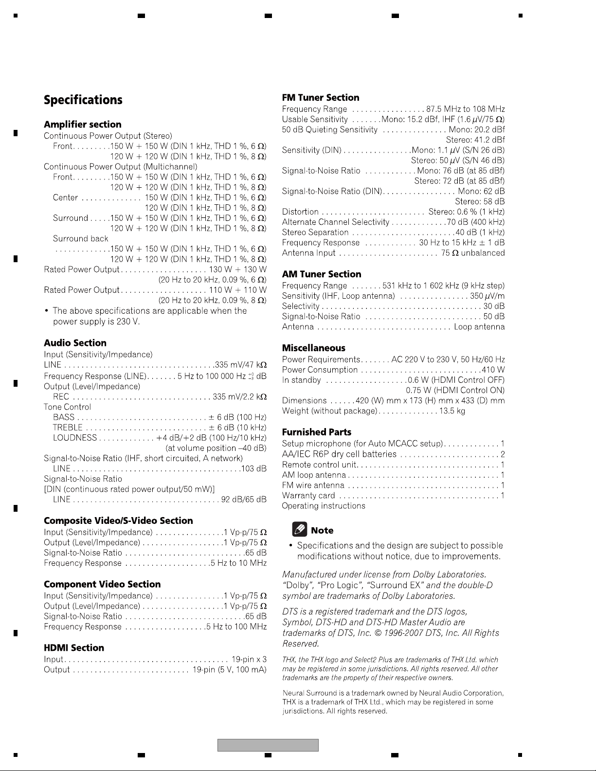
2. SPECIFICATIONS
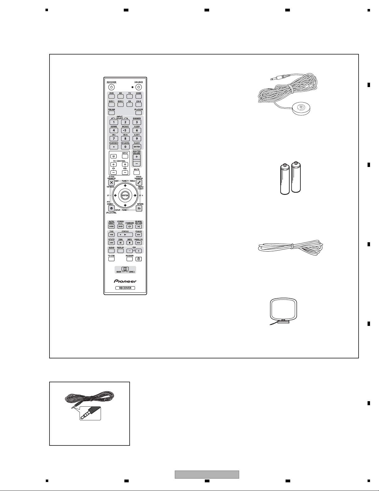
[1] Accessories
Remote Control Unit
(AXD7518: VSX-LX51)
(AXD7526: VSX-1018AH-K)
(AXD7527: VSX-1018AH-S)
Setup Microphone
(for Auto MCACC setup)
(APM7008)
AM Loop Antenna
(ATB7013)
FM Wire Antenna
(ADH7030)
AA/LR6 Dry Cell Batteries
(VEM1031)
SR+ mini-plug cable
(ADE7095)
SERVICE PARTS
2.1 ACCESSORIES
5
6 7 8
A
B
C
D
E
F
VSX-LX51
5
6 7 8
7
Page 8
1
(LX51)
13.3 kg (1018AH)
2.2 SPECIFICATIONS
A
B
2 3 4
C
D
E
F
8
1
2 3 4
VSX-LX51
Page 9
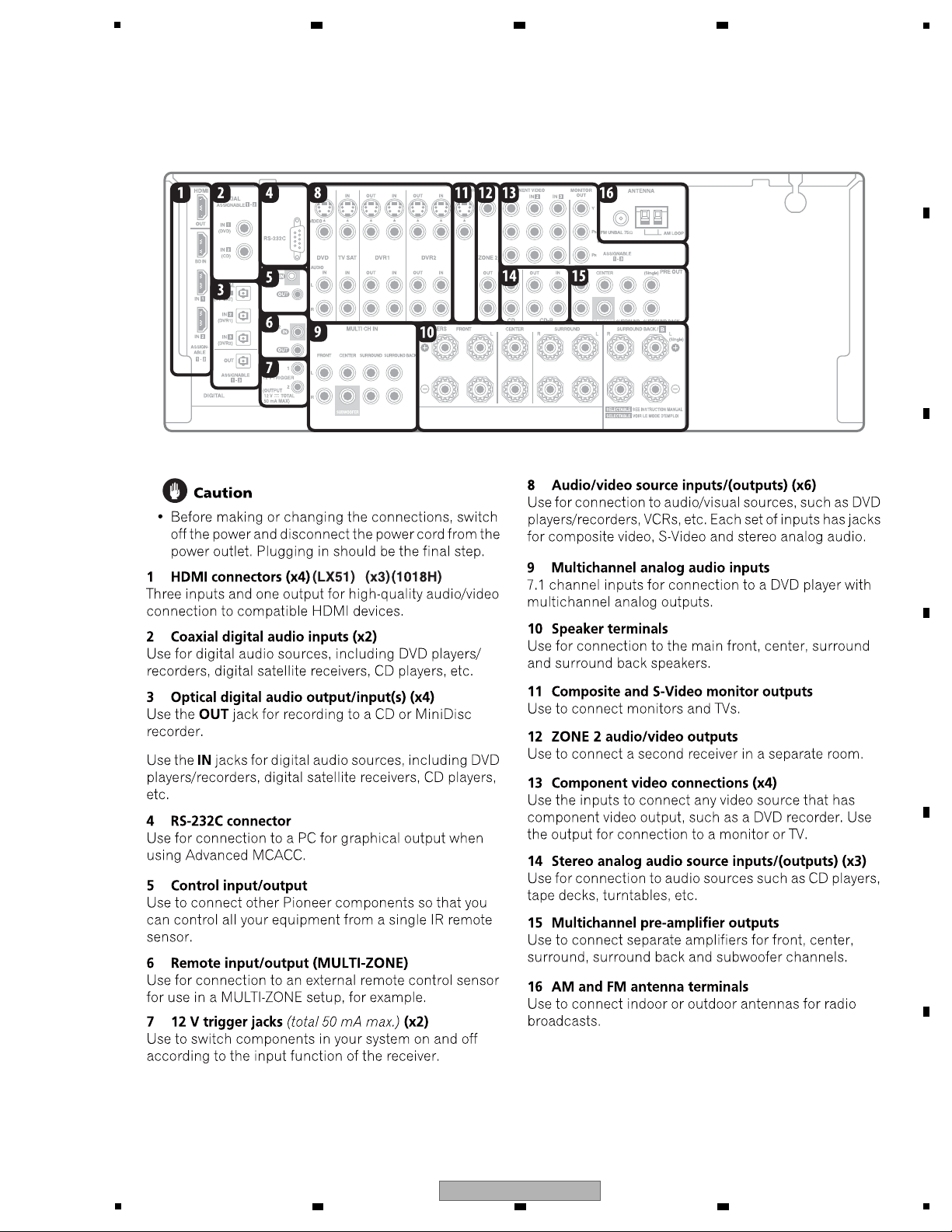
[1] Rear panel
VSX-LX51
5
2.3 PANEL FACILITIES
6 7 8
A
B
C
D
E
F
VSX-LX51
5
6 7 8
9
Page 10

1
VSX-LX51
[2] Front panel
A
B
2 3 4
C
D
E
F
10
1
2 3 4
VSX-LX51
Page 11
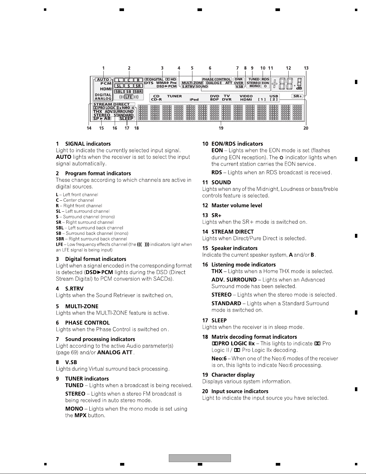
[3] Display
5
6 7 8
A
B
C
D
E
F
VSX-LX51
5
6 7 8
11
Page 12
1
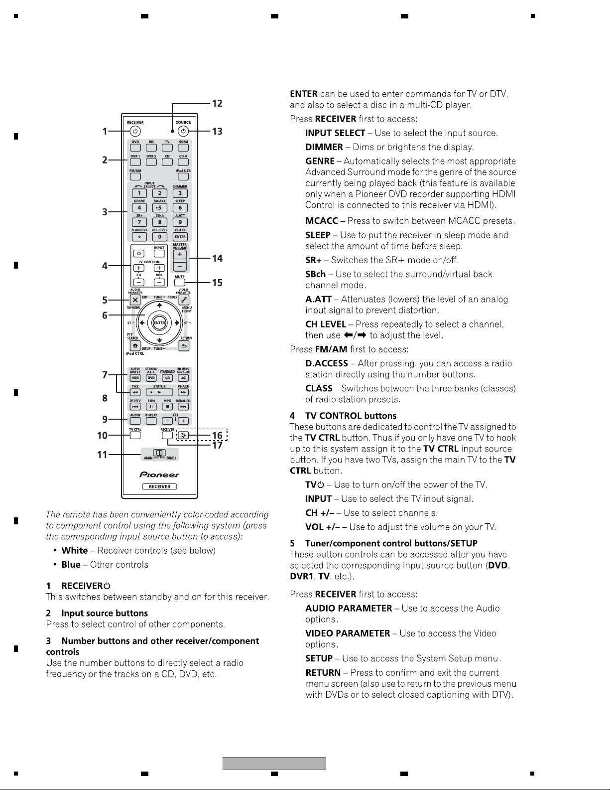
[4] Remote control
AXD7518
(VSX-LX51 Only)
A
B
2 3 4
C
D
E
F
12
1
2 3 4
VSX-LX51
Page 13
5
6 7 8
A
B
C
D
E
F
VSX-LX51
5
6 7 8
13
Page 14
1
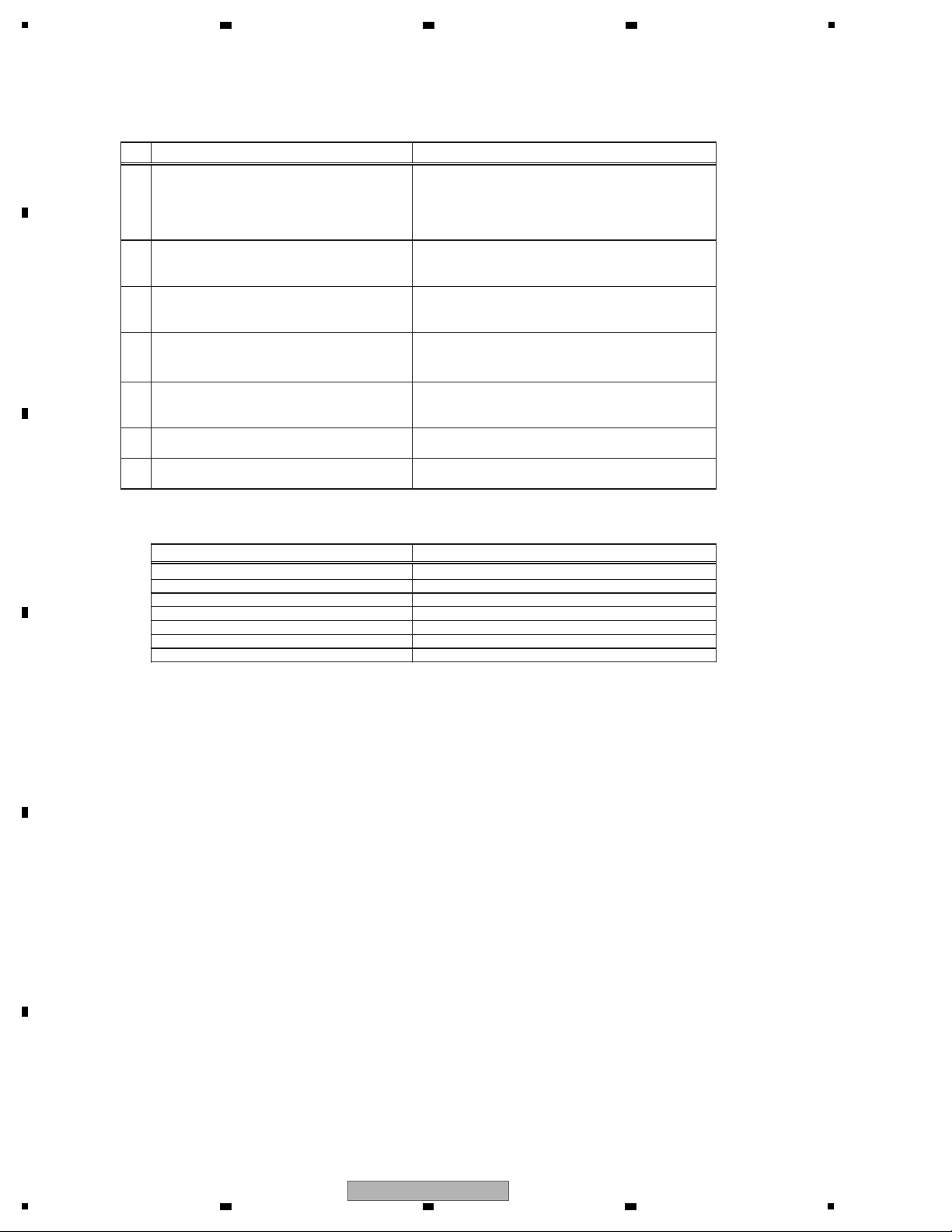
To keep the product quality after servicing, confirm recommended check points shown below.
No.
Procedure Check points
1
Confirm whether the customer complain has
been solved. If the customer complain occurs
with the particular source, such as Dolby
Digital, DTS, AAC, DVD-A and HDMI, input it
for the operation check.
The customer complain must not be reappeared.
Video, Audio and operations must be normal.
2
Check the analog audio playback.
(Make the analog connections with a DVD
player.)
Each channel audio and operations must be normal.
3
Check the digital audio playback.
(Make the digital connections with a DVD
player.)
Each channel audio and operations must be normal.
4
Check surround playback.
(Select Surround mode and check the
multichannel operations via the DSP circuit.)
Each channel audio and operations must be normal.
5
Check the video outputs.
(Connect with a DVD player.)
Video and operations must be normal.
6
Check the sound from headphone output. Sound must be normal, without noise.
7
Check the appearance of the product. No scratches or dirt on its appearance after receiving
it for service.
See the table below for the items to be checked regarding video and audio:
Items to be checked regarding video Item to be checked regarding audio
Block noise Distortion
Horizontal noise Noise
Dot noise Volume too low
Disturbed image (video jumpiness) Volume too high
Too dark Volume fluctuating
Too bright Sound interrupted
Mottled color
2 3 4
3. BASIC ITEMS FOR SERVICE
3.1 CHECK POINTS AFTER SERVICING
A
B
C
D
E
F
14
1
2 3 4
VSX-LX51
Page 15
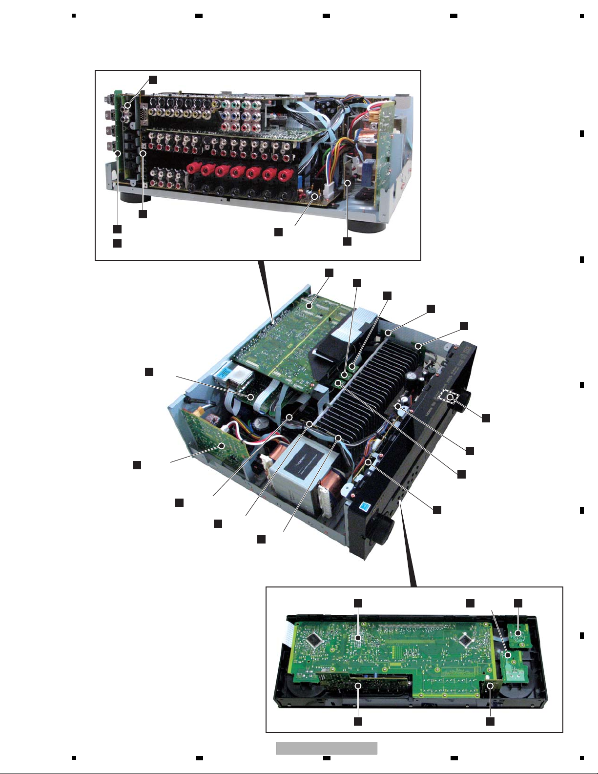
AUDIO IN ASSY
A
FRONT IN ASSY
D
DISPLAY ASSY
M
POWER SW
ASSY
O
MULTI JOG
ASSY
N
HEADPHONE ASSY
Q
REGULATOR ASSY
U
DC/DC ASSY
V
BINDER ASSY
H
POSI1 ASSY
W
POSI3 ASSY
Y
POSI2 ASSY
X
BIND_L_BACK
ASSY
J
BIND_L_FRONT
ASSY
I
PRIMARY
ASSY
T
PRE-STAGE AMP
ASSY
S
BIND_R_BACK
ASSY
L
BIND_R_FRONT
ASSY
K
HDMI&DVC ASSY
(VSX-LX51)
F
INTERFACE ASSY
E
DSP&USB ASSY
C
POWER AMP
ASSY
R
DIODE ASSY
P
HDMI ASSY
(VSX-1018AH-K,
VSX-1018AH-S)
G
MAIN ASSY
B
5
3.2 PCB LOCATIONS
6 7 8
A
B
C
D
E
VSX-LX51
5
6 7 8
F
15
Page 16

1
LIST OF ASSEMBLIES
Parts marked by "NSP" are generally unavailable because they are not in our Master Spare Parts List.
The mark found on some component parts indicates the importance of the safety factor of the part.
Therefore, when replacing, be sure to use parts of identical designation.
NOTES:
Mark Symbol and Description
VSX-LX51
/HYSXJ5
VSX-1018AH-K
/YSXJ5
VSX-1018AH-S
/YSXJ5
NSP
1..MAIN ASSY AWK8053 AWK8058 AWK8058
1..AUDIO IN ASSY AWK8051 AWK8051 AWK8051
1..COMPLEX ASSY AWK8047 AWK8064 AWK8064
2..DISPLAY ASSY AWX9117 AWX9214 AWX9214
2..POWER SW ASSY AWX9118 AWX9118 AWX9118
2..MULTI JOG ASSY AWX9119 AWX9119 AWX9119
2..BINDER ASSY AWX9120 AWX9120 AWX9120
2..FRONT IN ASSY A
WX9121 AWX9121 AWX9121
2..HEADPHONE ASSY AWX9122 AWX9122 AWX9122
2..PRIMARY ASSY AWX9124 AWX9124 AWX9124
NSP 1..LOCAL POWER ASSY AWK8041 AWK8041 AWK8041
2..DIODE ASSY AWX8985AWX8985AWX8985
2..REGULATOR ASSY AWX8986AWX8986AWX8986
2..DC/DC ASSY AWX8988 AWX8988 AWX8988
2..PRE-STAGE AMP ASSY AWX8989AWX8989AWX8989
2..INTERFACE ASSY AWX8990
A
WX8990 AWX8990
NSP 1..AMP ASSY AWK8038 AWK8038 AWK8038
2..POWER AMP ASSY AWX8984AWX8984AWX8984
2..POSI1 ASSY AWX9132 AWX9132 AWX9132
2..POSI2 ASSY AWX9133 AWX9133 AWX9133
2..BIND_L_FRONT ASSY AWX9217 AWX9217 AWX9217
2..BIND_L_BACK ASSY AWX9218 AWX9218 AWX9218
2..BIND_R_FRONT ASSY AWX9219 AWX9219 AWX9219
2..BIND_R_BACK ASSY A
WX9220 AWX9220 AWX9220
2..POSI3 ASSY AWX9223 AWX9223 AWX9223
1..HDMI&DVC ASSY AWX9170 Not used Not used
FLASH ROM AYW7203
1..HDMI ASSY Not used AWX9131 AWX9131
FLASH ROM
1..DSP&USB ASSY
FLASH ROM
AYW7203 AYW7203
AWX9176 AWX9176 AWX9176
AYW7213 AYW7213 AYW7213
1..FM/AM TUNER UNIT AXX7248 AXX7248 AXX7248
Not used Not used
Not used
A
2 3 4
B
C
D
E
F
16
1
2 3 4
VSX-LX51
Page 17

5
Name Jig No. Remarks
11P board to board extension jig
cable GGD1576
Diagonosis
19P board to board extension jig cable GGD1577
GGD1492
Diagonosis
Diagonosis
11P FFC
30P board to board extension jig cable
GGD1578
Diagonosis
RS-232C I/F jig GGF1348
Update the Flash ROMS
7-pin FFC VDA1681
Update the Flash ROMS
[1] Jigs list
3.3 JIGS LIST
6 7 8
A
B
C
D
E
F
VSX-LX51
5
6 7 8
17
Page 18
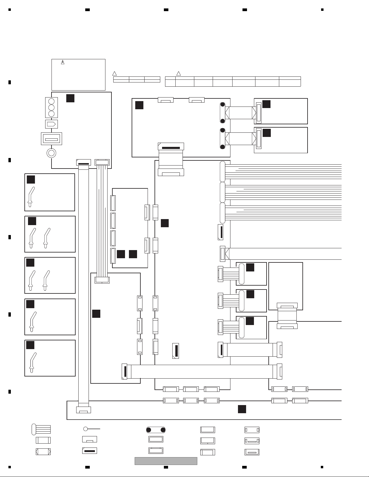
1
VEF1040-A
VEF1040-A VEF1040-A
VEF1040-AVEF1040-A
VEF1040-A
VEF1040-A
JA3601
JA3631
JA3641
JA3651
VIDEO IN
AUDIO IN
OPT IN
USB
MIC IN
CN3601
CN3602
*CN3001 *CN3002
CN3003
JH3001JH3002
CN3401 CN3501
CN109
J51 ADD7635
33/610
for download
JP3001
D20PDD0305E
D20PDD0405E
JP3002
CN1001CN1002
CN801
CN4809
J0 ADX7619
9/470(Shielded Cable)
J52 ADD7636
11/390
CN702
CN101CN102
CN118
CN703
CN704
CN104CN103
CN601
JP113JP117JP116
CN1401
CN116
CN111CN119CN112
CN7001CN7003CN7002
PG02KA-E07
PG03KS-E07
PG02KA-E07
CN110
CN506
J54 ADD7637
11/100
CN501
J55 ADD7638
23/180
*CN117
for service
CN106 CN107 CN108
CN4803CN4802CN4801
CN502CN503
CN4806
CN4805
11/60
CN1
ADD7639
J56
CN507
*4
4/400
ADX7652
PF09PG-R35
9/350
PF07PG-R40
7/400
JP3710
D20PDY0620E
J**
JP****
CABLE WIRE
1.25mm FFC
2.0mm FLAT CABLE
1.25mm FFC CONNECTOR(L)
CN****
CN****
(*1.00mm FFC CONNECTOR)
(*1.00mm FFC CONNECTOR)
1.25mm FFC CONNECTOR(I)
JH****
CN****
2.0mm CABLE HOLDER
2.0mm WIRE TRAP
KM200NA*
CN****
CN****
CN****
B*B-EH
EH CONNECTOR
ANOTHER TYPE
CODE SOCKET
1.25mm B to B
XKM****
XKP****
CN****
CN****
CN****
TUC-P**X-B1
1.25mm B to B
2.0mm B to B SOCKET
TUC-P**P-B1
2.0mm B to B CONNECTOR
!
HYS,YS
*1
T1501
ATT7419
AC CORD
VDG1080
*2
HYS,YS
REK1061
(T5AL/250V)
FU1 FU2,3
-
FU4
AEK1060
(T4AL/250V)
FU5
(T3.15AL/250V)
AEK1059
FU6,7
AEK7072
(T800mAL/250V)
FU8,9
(T2.5AL/250V)
AEK1058
!
*3
CN**
BOARD IN WIRE
CN****
of identical designation.
be sure to use parts
The
the importance of the
Therefore, when replacing,
safety factor of the part.
component parts indicates
mark found on some
FRONT IN ASSY
(AWX9121)
D
DISPLAY ASSY
(VSX-LX51 : AWX9117)
(VSX-1018AH-K, VSX-1018AH-S
: AWX9214)
M
POWER SW ASSY
(AWX9118)
O
MULTI JOG ASSY
(AWX9119)
N
HDMI & DVC ASSY
(VSX-LX51 : AWX9170)
F
HDMI ASSY
(VSX-1018AH-K,
VSX-1018AH-S : AWX9131)
G
MAIN ASSY
(VSX-LX51 : AWK8053)
(VSX-1018AH-K,
VSX-1018AH-S : AWK8058)
B
BIND_L_FRONT
ASSY (AWX9217)
I
BIND_L_BACK
ASSY (AWX9218)
J
DSP & USB ASSY
(AWX9176)
C
BINDER ASSY
(AWX9120)
H
BIND_R_FRONT
ASSY (AWX9219)
K
BIND_R_BACK
ASSY (AWX9220)
L
INTERFACE ASSY
(AWX8990)
E
FM/AM TUNER
UNIT
(AWX7248)
POSI 1
ASSY
(AWX9132)
W
POSI 3
ASSY
(AWX9223)
Y
POSI 2
ASSY
(AWX9133)
X
2 3 4
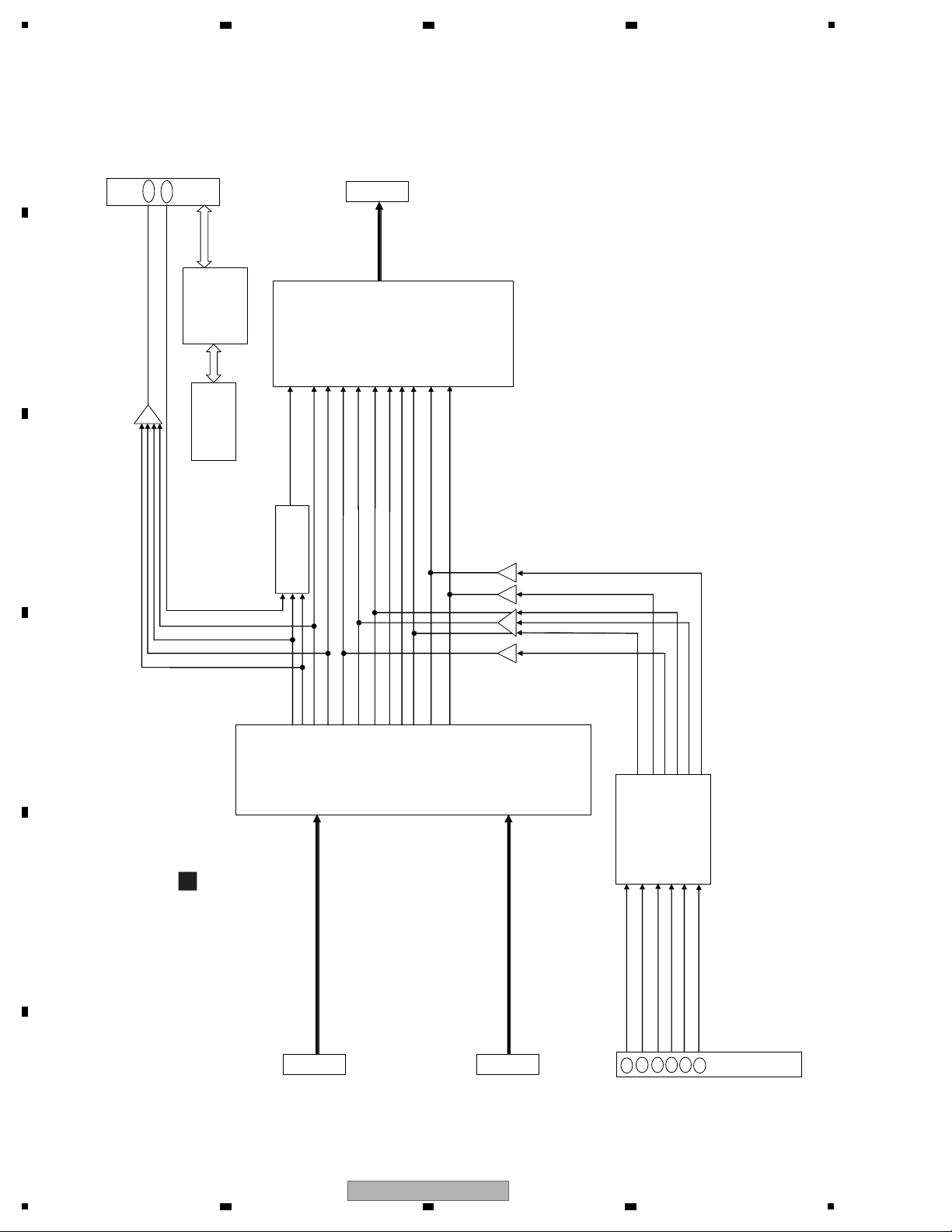
4. BLOCK DIAGRAM
4.1 OVERALL WIRING DIAGRAM
A
B
C
D
E
F
18
1
2 3 4
VSX-LX51
Page 19
5
CN504
CN4804
J58
19/165
ADD7641
CN6603
ADD7640
J57
17/75
CN505
CN6410 CN6110 CN6310 CN6610 CN6010 CN6510 CN6210
CN5410
CN5310
CN5210
CN5610
CN5010
CN5110 CN5510
CN5802
CN4807 CN4808
CN5803
CN4251
CN4004CN4003
CN4252
!
!
FU4
FU5
*3
!
FU6
FU7
!
FU8
FU9
!
!
CN4001
CN4071
JH3701
JP5750
PF04PG-R50
*3
MAIN TRANS
*1
!
T1501
FU2
FU3
FU1 !
!
!
CN3706 3709
CN3704
*3
CN5701
!
*2
AC CORD
JA3701
JA3702
CN4701
JH5801
CN3451
JP5801
D20PDY0460E
JP5701
ANOTHER TYPE
CN****
CN****
B to B SOCKET
ANOTHER TYPE
B to B CONNECTOR
HYS,YS
TUNER
MODULE
AXX7248
J56
ADD7637
FAN D-TERMINAL J59
--
-
*4 *5 *6
ADX7051
DC/DC ASSY
(AWX8988)
V
REGULATOR ASSY
(AWX8986)
U
PRIMARY ASSY
(AWX9124)
T
PRE-STAGE AMP ASSY
(AWX8989)
S
DIODE ASSY
(AWX8985)
P
HEADPHONE
ASSY
(AWX9122)
Q
POWER AMP ASSY
(AWX8984)
R
AUDIO IN ASSY
(AWK8051)
A
When ordering service parts, be sure to refer to "EXPLODED VIEWS and PARTS
LIST" or "PCB PARTS LIST".
The mark found on some component parts indicates the importance of the safety
factor of the part. Therefore, when replacing, be sure to use parts of identical
designation.
: The power supply is shown with the marked box.
4/500
6 7 8
A
B
C
D
E
F
VSX-LX51
5
6 7 8
19
Page 20
1
S
A
F
G
C
D
R Q
ER
IC101
HDMI
RECEIVER
SII9135CTU
OPT IN1
OPT IN2
OPT IN3
COAX
COAX
BD
HDMI IN1
HDMI IN2
IC1151
HDMI
SELECTOR
VIDEO
VIDEO
USB
MIC
IC801
USB HOST
LC87F1HC8A
IC101
DIR&DIT
AK4114VQ
OPT OUT
HDMI
IC202
USB
SELECTOR
IC203
HDMI
SELECTOR
IC401
1st DSP
DSPA56720AG
RX3
2ch DAC
192kHz/24bit
×4
IC251
BASICAUDIO
SELECTOR
IC301
HDMI
TRANSMITTER
SII9134CTU
IC591
2ch ADC
96kHz/24bit
IC681
DAC for 2nd ZONE
192kHz/24bit
TX0
I2S
I2S
CD
CD-R
TV/SAT
DVR1
DVR2
TUNER Module
DVD
MULTI IN L/R
MULTI IN SL/SR
MULTI IN SBL/SBR
MULTI IN C/SW
PREOUT L/R
PREOUT SW
PREOUT SL/SR
PREOUT SBL/SBR
CD-R REC
DVR1 REC
DVR2 REC
ZONE2 OUT
IC501
Selector / Volume / PRE Amp
BD3473KS2
IC503
ZONE2
E-VOL
M61545FP
SP L/R
SP C
SP SL/SR
SP SBL/SBR
HP
LPF
SW DownMix
IC601
IC621
IC641
IC661
JA1152
JA1151
JA1102
JA102
JA103
JA104
JA101
(1/2)
LX51 Only
JA301
JA105
(1018AH:HDMI IN1−>BD)
JA101
(2/2)
JA3601
JA3631
JA3651
JA3641
IC701
IC741
IC761
IC781
IC801
IC502,IC702
JA502
JA505
JA503
JA503
JA504
JA504
SW PRE Amp
IC821
NJM4565MD
<<POWER AMP>>
JA502
JA505
JA503
JA504
JA3451
JA5801
JA5801
JA5801
JA5802
JA5802
JA506
JA506
JA507
JA507
JA5803
JA5803
JA5804
JA5804
PREOUT C
JA506
2 3 4
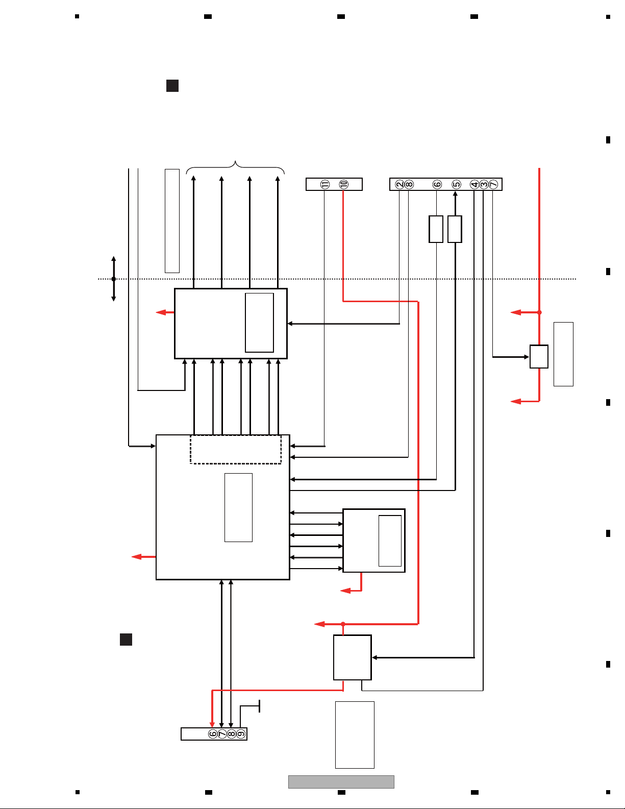
4.2 BLOCK DIAGRAM FOR AUDIO BLOCK
A
B
C
D
E
F
20
1
2 3 4
VSX-LX51
Page 21
DET
Sync
C
TC74HC4051AFT
IC1202
+
+
C
Y
Y
C
Y
C
Y
C
CCYYY
TC74HC4051AFT
IC1201
CN102
11
CN3601
CN108
IC1006
17 22
13
PDC162A
+
+
+
IC1203
TC74HC4053AFT
LA7109
IC1205
+
C
Y
Y
C
161420
18
CN102
24
+
TC74HC4053AFT
+
IC1003
+
+
TC74HC4051AFT
IC1001
+
TC74HC4051AFT
IC1002
+
LA7109
IC1004
13
4
5
2
3
15
14
1
12
2117
14 23
13
4
2
15
5
3
14
1
12
13
4
2
15
5
3
14
13
14 31
11 25
7
3
12
5
1
2
4
15
433
351
5
3
4
17
12
13
2
1
15
14
14
7
11
21
23
31
25
12
1
4
13
2
15
5
3
4
14
1
12
1
33
35
CVOUT
C Selector
DVR 2
6dB AMP
MUTE
MUTE
OUT
DVR 2
DVR 1
Y Selector
TV/SAT
DVD
to DVC
VIDEO
from DVC
OSD IC
for Video
Selector
DVR 2
Selector
Input
DVR 1
TV/SAT
Selector
for DVC/Through
MUTE
C
Y MUTE
OUT
DVR 1
MONITOR
OUT
from DVC
to DVC
for OSD/Through (VSX-1018AH)
Selector
for DVC/Through (VSX-LX51)
6dB AMP
MUTE
MUTE
OUT
MONITOR
OUT
DVR 1
DVD
MUTE
MUTE
Input Selector
for MR Video & OSD
OUT
DVR 2
ZONE 2
OUT
• COMPOSITE BLOCK
FRONT-IN ASSY
INTERFACE ASSY
D
E
MAIN ASSY
B
• S-VIDEO BLOCK
9
10
11
9
10
11
51C
51B
51A
9
10
11
51C
51B
51A
9
10
11
S53ABC
9
10
11
51C
51B
51A
M51C
M51B
9
10
V53C
V53B
M51A
20
13
30
3
20
13
30
3
Buffer
Buffer
Buffer
LX51 Only
LX51 Only
1018AH Only
1018AH Only
1018AH Only
IC1271
MAIN
5
6 7 8
4.3 BLOCK DIAGRAM FOR VIDEO BLOCK
A
B
C
5
D
E
F
21
VSX-LX51
6 7 8
Page 22
1
TC74LVX4052FT
IC1401
TC74LVX4053FT
IC1403
NJM2581M
IC1404
IC1402
TC74LVX4052FT
CN102
1
4
3
2
5
12
15
11
13
14
3
5
1
1
4
2
13
12
2
3
5
12
11
13
3
54
11
9
15
1
14
13
14
15
IN3
Cb
Cr
for DVC/Through
Y
Cr
IN2
Y
Cb
Cr
Cb
IN1
Selector
6dB AMP
Cr
Cb
COMPONENT OUT
Y
Y
Input Selector
Input Selector
from DVC
• COMPONENT BLOCK
MAIN ASSY
B
12 810 2 64
Buffer
Buffer
Buffer
9
10
C52A
C52B
9
10
C52A
C52B
9
10
11
C53ABC
to DVC
LX51 Only
1018AH Only
1018AH Only
COMPONENT
COMPONENT
COMPONENT
2 3 4
A
B
C
D
E
F
22
VSX-LX51
1
2 3 4
Page 23
5
HDMI IN2
HDMI OUT
HDMI IN1
BD IN
JA1151
(19P)
JA1152
(19P)
IC1151
IC101
IC301
SD[1:3]
HDSPDIF
DCK
HSYNC
D[0:5,8:9, 12:15,24:27]
D[16:23]
D[28:35]
JA301
(21P)
IC1301
FLI2310-LF-CF
IP Convert/Scaler
IC1351
IS42S32200E-6TL
64M SDRAM
4
141612
20
CN1002
(30P)
IC401
ADV7800BSTZ-80
VIDEO DECODER
VCV IN
VCY
IC601
ADV7172KSTZ
VIDEO ENCODER
VCV OUT
VCC
VCCY OUT
VCCb OUT
VCCr
P[22:29]
HS
VS
IC1381
TC74LCX541FTS1
IC1383
TC74LCX541FTS1
TC74LCX541FTS1
IC1384
IC202
ICS571LMF
MCLKO,BCKO,LRCKO,SD[0:3]O,SPDIFO
CN1001
(30P)
IC501
PEG118A
HDMI CPU
IC502
AYW7243
4M Flash ROM
TC74VHC541FTS1
JA1102
(19P)
IC251
TC74LCX157FTS1
AUDIO SELECTOR
HDMI RECEIVER
HDMI TRANSMITTER
HDMI SELECTOR
HDMCLK
MCLK,SCK,WS,SD0
26-
BAMCK,BABCK,BALRCK,BADAT
IC203
TC7WH74FU
IC204
TC7WH157FU
IC205
TC7WH157FU
D[6:7,10:11
SCK,WS,SD0
F
6 7 8
4.4 BLOCK DIAGRAM FOR HDMI FOR VSX-LX51
A
B
C
D
E
F
VSX-LX51
5
6 7 8
23
Page 24
1
HDMI IN
HDMI OUT
BD IN
JA1152
(19P)
IC101
IC301
SD[1:3]
HDSPDIF
DCK
VSYNCDEHSYNC
D[0:5,8:9,12:15,24:27
D[16:23]
D[28:35]
JA301
(21P)
8
10
12
18
20
24
CN1002
(30P)
IC401
ADV7800BSTZ-80
VIDEO DECODER
VCV IN
VCYINVCC IN
VCCY IN
VCCb IN
VCCr IN
P[22:29]
LLC
HS
VS
P[12:19]
IC1256
TC74LCX541FTS1
IC1257
TC74LCX541FTS1
TC74LCX541FTS1
IC1258
MCLKO,BCKO,LRCKO,SD[0:3]O,SPDIFO
6-15
CN1001
(30P)
IC501
PEG118A
HDMI CPU
IC502
AYW7243
4M Flash ROM
TC74VHC541FTS1
IC201
JA1102
(19P)
HDMCLK
MCLK,SCK,WS,SD0
26-
29
BAMCK,BABCK,BALRCK,BADAT
P[10:11,20:21]
D[6:7,10:11
SCK,WS,SD0
IC251
TC74LCX157FTS1
IC1259
TC7SZ125FU
G
HDMI RECEIVER
HDMI TRANSMITTER
AUDIO SELECTOR
2 3 4
4.5 BLOCK DIAGRAM FOR HDMI FOR VSX-1018AH
A
B
C
D
E
F
24
VSX-LX51
1
2 3 4
Page 25
5
IC808
341S2154
IC851
TC74VHC157
IC802
AAT4618
CN801
D+
D-
SPI_SIMO
SPI_UCLK
SPI_nSS
CPRST
CPRDY
SPI_SOMI
UMCKIMCK
OSCU
ULR
UBCK
MSSS
ILRCK
IBCLK
MSCK
ISDAT
MSDA
UDT
to IC202
IPIF_SW
UASW
USBCTL
V5USB
D-
D+
GNDD
V5DU
XFLAG
CN701
CN702(KU model)
IPIF SW
USB AUDIO SW
USB CTRL
USB XFLAG
CN704
V+5D
(from IC503)
24.576MHz
from IC705Q871
Q872
USB POWER
USB RESET
USB DAI
USB DAO
IC801
PDC180A8
USB U-Com
(FLASH built-in)
5=>3
3=>5
IC701
IC702
12
11
218
V+3DU V3D
V+3DU
V+3DU
V+3DU
37
38
USBREQ
OSCU
(from IC401 83p)
Audio OUTPUT
28
3427332631
18
USBRST
USB DAI
USB DAO
12
13
14
22
21
1
45
44
2
15
USBREQ
46
Digital Audio
Signal selector
SW
USB Power SW
iPod
authentication
IC
USB Bus Power
Control
(Over Current
detection)
USB Block DSP Block
Digital Audio Signal Output
C
C
6 7 8
4.6 BLOCK DIAGRAM FOR USB BLOCK
A
B
C
D
5
E
6 7 8
VSX-LX51
F
25
Page 26
1
u-com
RENESUS
M32C/87
DPS Control
144pin
OSD IC
HDMI Control
u-com
RENESUS
M16C/62P
HDMI/DVC
VIDEO SW IC
DSP
Expantion
Port IC
TUNER
MODULE
RDS IC
VOLUME
FUNCTION
IC
FL
USB
(SANYO
USB)
EEPROM
64kbyte
PE5615A-K
FL Driver
u-com (100p, 5V)
•FL,LED
PDC158A8
Event u-com
(100p, 5V)
•KEY,REMOTE
MAIN
IC801
IC401
IC401
IC601
(LX51 only)
IC1005
IC3001
V3001
IC3004
IC1006
IC261
IC501
IC1405
IC501
IC202
IC101
IC1001,IC1002,IC1003
IC1201,IC1202,IC1203
IC1401,IC1402,IC1403
A
F G
F G
C
C
M
M
M
B
B
B
B
B
B
2 3 4
4.7 BLOCK DIAGRAM FOR U-COM
A
B
C
D
E
F
26
1
2 3 4
VSX-LX51
Page 27
5
MAIN ASSY
REGULATOR ASSY
PRIMARY ASSY
FU1
T3701
STBY
TRANSFORMER
ATT7040(HYS)
RY
IC3701
NJM78M56
+5.6V
AC
T1501
POWER
TRANSFORMER
ATS7419(HYS)
IC4004
NJM78M05
+5V
IC4005
NJM78M56
+5.6V
IC4006
NJM79M05
-5.6V
FL POWER
SUPPLY
BLOCK
IC5763
BA178M12
+12V
IC5751
NJM78M12
+12V
IC5752
NJM79M12
-12V
VL SELECTOR
+VH
SUPPLY
BLOCK
-VH
SUPPLY
BLOCK
POWER AMP ASSY
IC4251
PQ1CG3032
+5V
DC/DC ASSYHDMI ASSY
DSP ASSY
V+5AD
V+13UN
V+5D
VIDEO BLOCK
V-5.6V
V+5.6V
DISPLAY ASSY
IC3001
FL
u-com
IC3004
EVENT
u-com
LED BLOCK
KEY BLOCK
IC101
MAIN
u-com
MUTE Logic
232C Logic
RDS / Logic
3-5 / 5-3
V+5.6U
V+5.6ST
FL AC
V-VF
FL
DISPLAY
POWER AMP
BLOCK
±VL
PRESTAGE-AMP
ASSY
±VH
INTERFACE
ASSY
FRONT IN ASSY
AUDIO
ASSY
12V
TRG
232C
/ IR
V+12TRG
±7V
Rough
Lock
V+5OPT
V±7A
IC501
E-VOL
V±12A
LPF
PRE Amp
TUNER Module
V+9T
VSX model only
+9V
Rough
Lock
V+12T
+5V
Rough
Lock
+3V
Rough
Lock
-5V
Rough
Lock
-3V
Rough
Lock
V-3C
V+3C
V-5V
V+5V
IC1001
BD9011KV
+3.3/2.5V
IC1071
NJM78M05
+5V
IC1051
PQ200WNA1
+5V
IC704
BD9107FVM
+1V
IC705
PQ1LAX95M
+3.3V
A/D
comv.
R
U
S
E
A
V
F
G
C
D
M
B
T
6 7 8
4.8 BLOCK DIAGRAM FOR POWER SUPPLY BLOCK
A
B
C
D
5
6 7 8
VSX-LX51
E
F
27
Page 28
1
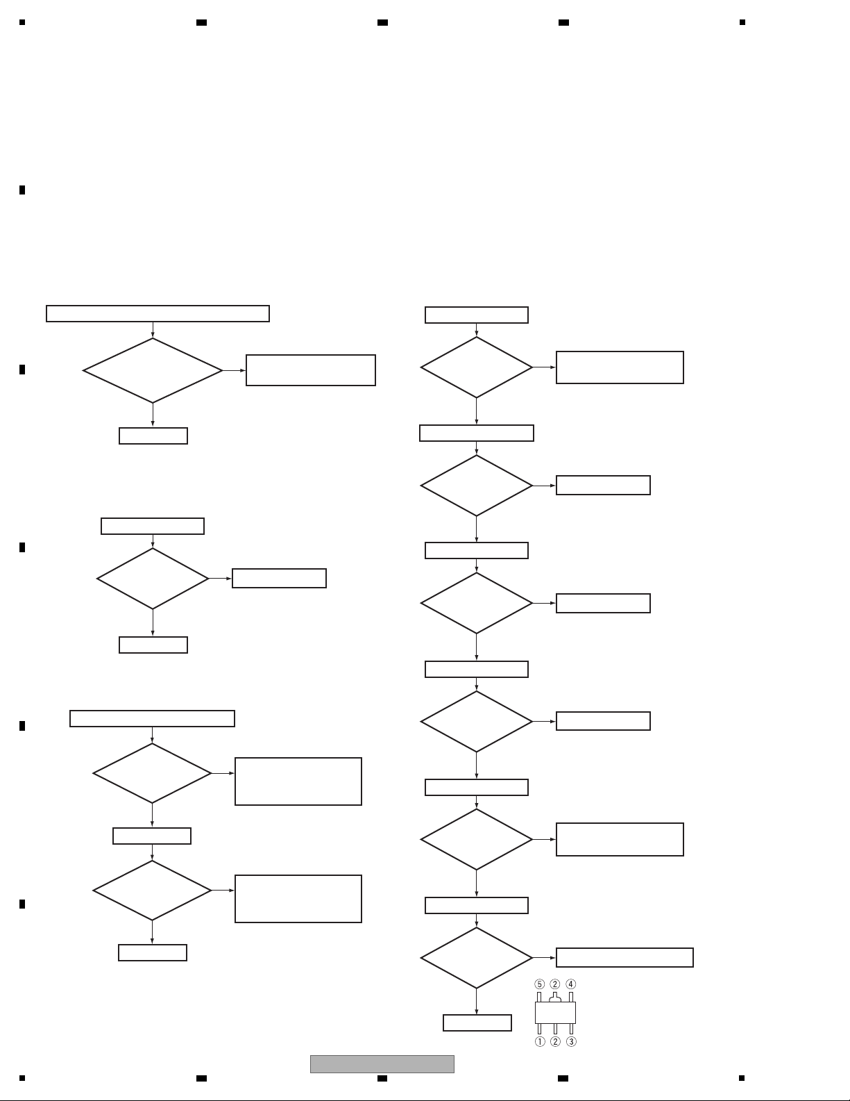
Step 1: MUTE pin
Replace IC401.
Check the IC705.
Replace IC705.
To Step 2
To Step 4
Step 0: Preliminary confirmation
Confirm the following items before checking
Do screws
of COAX Jack
securely tighten
?
Tighten screws securely.
Note:
If this section is not fixed,
the GND for DSP module
may lifted from the chassis
and cause instable potential
and lead to product failures.
No
Ye s
To Step 1
IC401 (Pin 84)
Is the
voltage of output
signal 0 V
?
No
Ye s
DS0MUT3
Step 3: Regulator IC
Check the IC704 and
REGULATOR Assy.
Check the Q601 and
REGULATOR Assy.
IC704 (Pins 7,8)
Is the
voltage of around
5 V to 5.3 V
input?
No
Ye s
(to chassis)
IC705 (Pin 5)
Is the
voltage of 3.3 V
output?
No
(to chassis)
IC705 (Pin 4)
Is the
voltage of around
5 V to 5.3 V
output?
No
Ye s
Ye s
Replace IC704.
L705, L704 (stby side)
Is the
voltage of 1 V
output?
No
Ye s
(to chassis)
Replace Q601 and Q561.
Q601 (Pins 1, 2, 5, 6)
Is the
voltage of 5 V
output?
No
Is the
voltage of 5 V
input?
Q601 (Pin 4)
No
Ye s
Ye s
(to chassis)
(to chassis)
Part shape and Pin arrangement
of IC705
Step 2: BtoB connector and FFC
CN702, CN703, CN704, CN801
Are the
connectors securely
inserted?
Turn the power off and
insert the connectors
securely.
No
Ye s
CN601
Is the
FFC securely
inserted?
Turn the power off and
insert the connectors
securely.
No
Ye s
To Step 3
BtoB connector
FFC
Simplified diagnosis
Errors in DSP Assembly (Areas simply and roughly predictable by machine operation only)
• Sound abnormality in Delay
If sound abnormality does not occur in the Delay OFF state but occurs in the Delay ON state, it is most likely
that a failure has occurred in SDRAM (IC301) or LATCH (IC303, IC304) in the 1st DSP Block.
• No sound at analog signal input
If sound abnormality does not occur with a digital signal input (COAX, OPT) but occurs only with an analog signal input,
it is most likely that a failure has occurred in the AD converter (IC591).
Troubleshooting
[1] DSP Troubleshooting
2 3 4
5. DIAGNOSIS
5.1 DIAGNOSIS FLOWCHART
A
B
C
D
E
F
28
1
VSX-LX51
2 3 4
Page 29
5
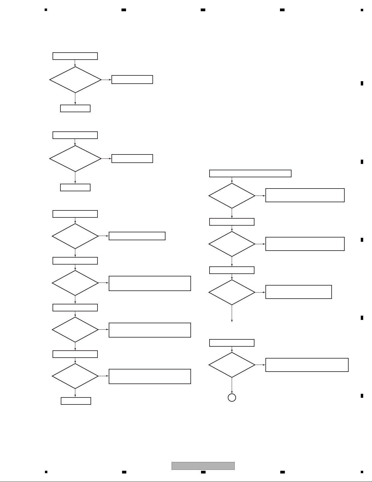
Step 7-1: DIR
Step 7
A
To Step 6
Check the parts and patterns
in the path.
Check the HDMI ASSY, and the parts
and patterns in the path.
IC701
Do
convert 5 V into
3 V for input?
Replace IC701.
No
Ye s
Check the OPTICAL IN JACK,
and parts and patterns in the path.
Check the pattern to pin 10 of IC851.
Replace IC851.
Check the FRONT IN ASSY, and
parts and patterns in the path.
IC101 (Pins 1, 3, 5 (VSX-LX51 only))
OPTICAL
Check that the S/PDIF signal is output.
Check that changes by pulling out and inserting the
digital input lines.
When the COAX or OPT is input, go to Step 7-1.
When the USB is input, go to Step 7-2.
When the HDMI (SPDIF line) is input, go to Step 7-1.
Used Source
[dts HD High Resolution Audio], [dts HD LBR],
[Dolby Digital Plus], [2ch of 48kHz sampling rate or less],
[Other compression stream]
When the HDMI (I2S line) is input, go to Step 7-3.
Used Source
[dts HD Master Audio], [Dolby True HD],
[PCM or LPCM of 88.2kHz sampling rate or more],
[LPCM Multi ch]
When the HDMI (SACD) is input, go to Step 7-5.
Used Source [SACD]
Can
observe the
digital signal
?
No
(0 V ⇔ 4 V)
Ye s
(0 V ⇔ 4 V)
IC101 (Pins 42, 44)
COAX
Can
observe the
digital signal
?
No
Ye s
Ye s
Check that it changes in the Playback and Pause modes of
the HDMI.
(0 V ⇔ 3.3 V)
IC101 (Pin 48)
From HDMI ASSY
Can
observe the
digital signal
?
No
(1.65 V center, amplitude more than 0.2 Vp-p)
IC101 (Pin 7)
FRONT OPTICAL
Can
observe the
digital signal
?
No
Ye s
Step 6: X'tal
To Step 7
Replace IC503 or X531.
Ye s
IC503 (Pin 6)
No
Is there
a 24.576 MHz
output?
Check the pattern to pin 30 of IC101.
Replace IC101.
IC503 (Pin 12)
No
Is there
a 24.576 MHz
output?
Check the pattern to pin 80 of IC401.
Replace IC401.
Ye s
Ye s
IC503 (Pin 10)
No
Is there
a 24.576 MHz
output?
Ye s
IC503 (Pin 8)
No
Is there
a 24.576 MHz
output?
Step 5: 5 V to 3 V conversion
Step 4: 3 V to 5 V conversion
IC702
Do
convert 3 V into
5 V for input?
To Step 5
Replace IC702.
No
Ye s
6 7 8
A
B
C
D
5
VSX-LX51
6 7 8
E
F
29
Page 30
1
Replace IC101.
Ye s
IC101 (Pin 26)
DIRB (Bit clock)
No
Is there
a bit clock
output?
(0 V ⇔ 3.3 V)
To Step 7-3
Ye s
IC202 (Pin 4)
S2DT (Data)
Is there
a data
output?
(0 V ⇔ 3.3 V)
Ye s
IC202 (Pin 7)
S2BC (Bit clock)
Is there
a bit clock
output?
(0 V ⇔ 3.3 V)
Ye s
IC202 (Pin 12)
S2LR (LR clock)
Is there
a LR clock
output?
(0 V ⇔ 3.3 V)
To Step 7-2
Ye s
IC202 (Pin 9)
S2MC (Master clock)
Is there
a master clock
output?
(0 V ⇔ 3.3 V)
Replace IC202.
At COAX, OPT, HDMI or SPDIF input
Check the path
between Pin 1 of IC202
and microcomputer.
Check the path
between Pin 1 of IC202
and microcomputer.
No
No
No
No
No
Is the
voltage Pin 1 of
IC202 at
0 V?
Ye s
Replace IC202.
At USB input
No
Is the
voltage pin 1
of IC202 at
5 V?
Ye s
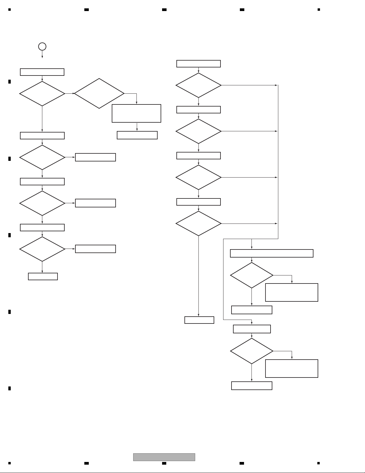
Step 7-2: Switch
Check that the data and clock signals are output.
A
Replace IC101.
(0 V ⇔ 3.3 V)
Ye s
IC101 (Pin 24)
DIRL (LR clock)
No
Is there
a LR clock
output?
Replace IC101.
(0 V ⇔ 3.3 V)
Ye s
IC101 (Pin 25)
DIRD (Data)
No
Is there
a data
output?
Replace IC101.
(0 V ⇔ 3.3 V)
Check the other assy.
(peripheral circuit of
the microcomputer)
IC101 (Pin 23)
DIRM (Master clock)
No
No
Ye s
Is there
a master clock
output?
Is the
voltage Pin 31
(PDN input signal)
of IC101 at
5 V?
No
Check that the data and clock signals are output.
A
2 3 4
B
C
D
E
F
30
1
2 3 4
VSX-LX51
Page 31

5
To Step 8
Ye s
IC205 (Pin 6)
SDTI (Data)
Is there
a data
output?
(0 V ⇔ 3.3 V)
Ye s
IC205 (Pin 8)
CDTI (Data)
Is there
a data
output?
(0 V ⇔ 3.3 V)
No
No
Replace IC205.
Is the
voltage Pin 4 /
Pin 10 of IC205
at 3.3V?
Ye s
Step 7-4: Switch
Check that the data is output. (Sch and Cch Signal having)
Ye s
IC203 (Pin 4)
FDTI (Data)
Is there
a data
output?
(0 V ⇔ 3.3 V)
Ye s
IC203 (Pin 7)
BCKI (Bit clock)
Is there
a bit clock
output?
(0 V ⇔ 3.3 V)
Ye s
IC203 (Pin 12)
LCKI (LR clock)
Is there
a LR clock
output?
(0 V ⇔ 3.3 V)
Ye s
IC203 (Pin 9)
MCLK (Master clock)
Is there
a master clock
output?
(0 V ⇔ 3.3 V)
Replace IC203.
At COAX, OPT, HDMI SPDIF or
USB input
Check the path
between Pin 1 of IC203
and microcomputer.
No
No
No
No
No
Is the
voltage Pin 1 of
IC203 at
0 V?
Ye s
Replace IC203.
At HDMI (I2S) input
Check the path
between Pin 1 of IC203
and microcomputer.
No
Is the
voltage Pin 1 of
IC203 at
5 V?
Ye s
Step 7-3: Switch
Check that the data and clock signals are output.
To Step 7-4 (For I2S line in the HDMI input)
To Step 8 (For other line)
6 7 8
A
B
C
D
E
F
VSX-LX51
5
6 7 8
31
Page 32

1
Step 8: DSP output (digital)
Ye s
Digital output of each CH when inputting the digital
signal with audio.
Replace IC401.
IC401 (Pin 124)
Surround L/R data
No
Is the output
0 V fixing?
B
Replace IC401.
Ye s
IC401 (Pin 123)
Center/LFE data
No
Is the output
0 V fixing?
Ye s
IC401 (Pin 123)
Center/LFE data
No
Is there
a data output?
Ye s
IC401 (Pin 124)
Surround L/R data
No
Is there
a data output?
Ye s
IC401 (Pin 125)
Front L/R data
No
Is there
a data output?
(0 V ⇔ 3.3 V)
(0 V ⇔ 3.3 V)
(0 V ⇔ 3.3 V)
Digital output of each CH when inputting the digital
signal (-∞ dB (no audio)).
To Step 8
Ye s
IC203 (Pin 4)
DSDFL (DSD data)
Is there
a data
output?
(0 V ⇔ 3.3 V)
Ye s
IC203 (Pin 7)
BCKI (DSD clock)
IC205 (Pin 3)
DSDFR (DSD data)
Is there
a clock
output?
(0 V ⇔ 3.3 V)
(0 V ⇔ 3.3 V)
No
No
Step 7-5: Switch (SACD only)
Check that the data and clock signals are output.
Check that the data signal is output.
Replace IC203.
Check the path
between pin 1 of IC203
and microcomputer.
No
Is the
voltage Pin 1
of IC203 at
5 V?
Ye s
Ye s
IC401 (Pin 122)
Surround Back L/R data
No
Is there
a data output?
(0 V ⇔ 3.3 V)
Replace IC401.
There is a possibility
of the Boot error.
(Identification of the
defective part near
DSP is extremely
difficult.)
No
Ye s
Ye s
Is there
a data
output?
(0 V ⇔ 3.3 V)
Ye s
IC205 (Pin 11)
DSDSL (DSD data)
Is there
a data
output?
No
No
Replace IC205.
Check the path
between Pin 1 /
Pin 13 of IC205
and microcomputer.
No
Is the
voltage of pin 1/
pin 13 of IC205
at 0 V?
Ye s
Is the
voltage of
DS0RST at 3.3 V?
(Does it drop to 0V
periodically?)
A
2 3 4
B
C
D
E
F
32
1
2 3 4
VSX-LX51
Page 33

5
Replace IC621.
Ye s
IC621 (Sch) (Pin 8)
Surround R out
No
Is there
a data output?
Replace IC601.
Ye s
IC601 (Fch) (Pin 11)
Front L out
No
Is there
a data output?
Replace IC601.
Ye s
IC601 (Fch) (Pin 8)
Front R out
No
Is there
a data output?
Step 9: DAC output (analog)
Analog output of each CH when inputting the digital
signal with audio.
Replace IC641.
Ye s
IC641 (Cch) (Pin 11)
Center out
No
Is there
a data output?
Replace IC641.
Ye s
IC641 (Cch) (Pin 8)
LFE out
IC401 (Pin 122)
Surround Back L/R data
No
Is there
a data output?
Replace IC661.
Ye s
IC661 (SBch) (Pin 11)
Surround Back L out
No
Is there
a data output?
Replace IC661.
Ye s
IC661 (SBch) (Pin 8)
Surround Back R out
No
Is there
a data output?
Replace IC621.
Ye s
IC621 (Sch) (Pin 11)
Surround L out
No
Is there
a data output?
Ye s
Replace IC401.
IC401 (Pin 125)
Front L/R data
No
Is the output
0 V fixing?
Ye s
Replace IC401.
No
Is the output
0 V fixing?
B
C
IC501 (Pin 3)
DAMC (Master clock)
Ye s
Replace IC501.
No
Is there
a master clock
output?
Check that the clock signal is output.
(0 V ⇔ 3.3 V)
IC501 (Pin 6)
DABC (Bit clock)
Ye s
Replace IC501.
No
Is there
a bit clock
output?
(0 V ⇔ 3.3 V)
(0 V ⇔ 3.3 V)
IC501 (Pin 11)
DALR (LR clock)
Ye s
Replace IC501.
No
Is there
a LR clock
output?
To Step 9
6 7 8
A
B
C
D
E
F
VSX-LX51
5
6 7 8
33
Page 34

1
Replace IC621.
Ye s
IC621 (Sch) (Pin 8)
Surround R out
No
Replace IC601.
Ye s
IC601 (Fch) (Pin 11)
Front L out
No
Replace IC601.
Ye s
IC601 (Fch) (Pin 8)
Front R out
No
Replace IC641.
Ye s
IC641 (Cch) (Pin 11)
Center out
No
Replace IC641.
Ye s
IC641 (Cch) (Pin 8)
LFE out
No
Replace IC661.
Ye s
IC661 (SBch) (Pin 11)
Surround Back L out
No
Replace IC661.
Ye s
IC661 (SBch) (Pin 8)
Surround Back R out
No
Replace IC621.
Ye s
IC621 (Sch) (Pin 11)
Surround L out
No
C
Analog output of each CH when inputting the digital
signal (-∞ dB (no audio)).
End
Is the output
2.5 V fixing?
Is the output
2.5 V fixing?
Is the output
2.5 V fixing?
Is the output
2.5 V fixing?
Is the output
2.5 V fixing?
Is the output
2.5 V fixing?
Is the output
2.5 V fixing?
Is the output
2.5 V fixing?
A
2 3 4
B
C
D
E
F
34
1
VSX-LX51
2 3 4
Page 35

5
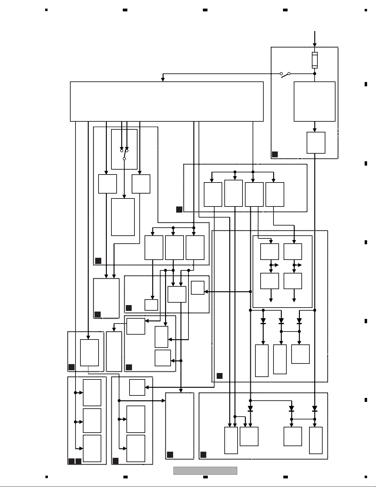
DSP Block Diagram
I2S MCLK
I2S DATA (2ch)
I2S DATA (Compression Include(dts HD High Resolution Audio, dts HD LBR, Dolby Digital Plus) or 2ch(under 48KHz for HDMI))
I2S or DSD DATA (from HDMI "dts HD Master Audio" "Dolby TrueHD" "SACD" "LPCM Multi" "PCM over 88.2KHz or LPCM")
I2S LRCK, BCK
Control/Memory Bus Line,etc
Analog Audio Signal
SPDIF,Operation Clock,etc
V1D(1.0V)
IC704
V5A CN704
BD9107FVM
3
V5D
V3D(3.3V)
IC705
PQ1LAX95MSPQ
8,9
CN601
Analog in(L/R)
21,23
Analog 8ch OUT
SPDIF out(1)
OPT Jack on-board
JA105
COAX in(2) CN601
JA101
24.576MHz
JA102 SPDIF in
OPT Jack 3 on-board
JA103
IC503
74VHCU04
CN703
CN801
Control in
3
Control out
CN704
13
19,20
18
22
15-18
74VHC125
IC205
CN704
V5DU
CN703
10
30,28
29
26 IC401
747SH32FU
Pin No. SACD Signal Other Signal
IC751
85 Data(C) -
86 Data(SW)-
97 Data(FL) Data(FL,FR)
98 Data(FR) Data(SL,SR)
99 Data(SL) Data(C,SW)
Data(SR) Data(SBL,SBR)100
Buffer
IC501
74LCX08
SW
IC203
74LCX157
LR/BCKI
SDI0_1 DSP
MCLK IC401
DSPA56720AG
SDI1_1~SDI3_1
SDI0~SDI1
ADC
IC591
AK5358AET
FLASH
ROM
IC302
AYW7247
SDRAM
IC301
64Mbit
(4bank*1M
*16bit)
MCLK LR/BCKO
DTO
HDMI in
HDMI out (Basic Audio)
DIR
IC101
AK4114VQ
USB
Block
(SANYO)
A2-BAF30405
(5/5)
SW
IC202
74VHC157
IC702
74VHCT541
IC701
74VHC08
DAC
WM8728
×4
DAC
WM8728
×4
DAC
WM8728
×4
2ch DAC
IC601-IC661
WM8728×4
CN601
for 2nd zone
USB Analog
2ch OUT
DAC
IC681
AK4388ET
6 7 8
A
B
C
D
E
F
VSX-LX51
5
6 7 8
35
Page 36

1
DSP Power Block and GND MAP
CN703
GNDD
5V
1.0V
Logic ICs
5V
3.3V DSP
3.3V & 1.2V
GNDD
Flash ROM
SDRAM
Logic ICs
3.3V
GNDD
DSP OSC
Logic ICs
3.3V
GNDD
DIR
5V & 3.3V
GNDD
2ch ADC 2ch DAC x4
5V
COAX
GDAC GDAC GNDD
CN601 CN704 GCH
uGRTN
DGRTN
DGRTN
GNDA(DAG)
V+5A
V+5D
V+5D(USB)
GNDD
REG
GNDA(DAG)
DC-DC
GNDD
GNDD
GNDA(DAG)
V+5D
DGRTN
GNDD
GNDD
GNDD
GNDD
GNDD
GNDD
Zone2 DAC
A5V
A
2 3 4
B
C
D
E
F
36
1
2 3 4
VSX-LX51
Page 37

5
Conditions for selecting SPDIF or I2S output
pcm fs(kHz) I2S(3 lines)SPDIFLayout
Compression DVD-V 48
Compression *.WAV 44
48
dts-CD 44
PCM 44
48
DVD-V
96 2ch
LPCM 44
Multi
48 2ch
Multi
88 2ch
Multi
DVD-A
96 2ch
Multi
176
Multi
192 2ch ×
2ch ×
×
×
×
2ch ×
2ch ×
2ch ×
2ch ×
2ch ×
2ch ×
×
2ch
Multi - -
--
SACD 2ch
(DSD)
Multi
×
× (DSD)
dts HD Master Audio
dts HD High Resolution Audio ×
dts HD LBR
×
Dolby TrueHD
×
×
Dolby Digital Plus
×
Indistinguishable
6 7 8
A
B
C
D
E
F
VSX-LX51
5
6 7 8
37
Page 38

1
1. Causes for noncompletion of HDMI authentication between the source equipment and this unit
(the HDMI indicator is unlit or flashes)
[2] HDMI Simple Diagnosis
Replace the HDMI cable.
NG
OK
OK
OK
Replace the Receiver.
Replace the Player.
Replace the HDMI cable.
Repare the Receiver.
Repare the Player.
NG
2. Causes for noncompletion of HDMI authentication between the monitor and this unit
(no display or sound from the monitor)
Replace the HDMI cable.
NG
OK
OK
OK
Replace the Receiver.
Replace the TV monitor.
Replace the HDMI cable.
Repare the Receiver.
Repare the TV monitor.
NG
A
2 3 4
B
C
D
E
F
38
1
VSX-LX51
2 3 4
Page 39

5
[3] Preparations for HDMI diagnosis
Note : Even if the unit shown in the photos and illustrations in this manual may differ from your product, the procedures
described here are common.
Jig cable
• Extension jig cable (GGD1492) x2
• 11P board to board extension jig cable (GGD1576)
• 19P board to board extension jig cable (GGD1577) x2
• 11P FFC (GGD1578)
Position of Wire Styling (The above angle is different.)
Position of Wire Styling
[Procedures]
1
Remove the Rear Panel.
3
Remove the two screws that fix the HDMI Shield V5S.
2
Remove the screw that fix the MAIN Assy and the Wire Styling of the PCB Binder.
4
Connect the four extension jig cables (two 19P board to board extension jig cable, one 11P board to board extension jig cable and 11P FFC).
5
Raise the MAIN Assy with the HDMI&DVC Assy and DSP&USB Assy attached and place it on the Heat Sink V5S.
Fix the lower part of the HDMI&DVC Assy with the PCB Binder.
6
Connect the earth point.
CN110
CN108
CN506
19P board to board
extension jig cable
(GGD1577)
4
11P board to board
extension jig cable
(GGD1576)
11P FFC
(GGD1578)
4
CN506
CN110
CN4801
CN4802
CN4803
CN107
CN106
11P FFC
(GGD1578)
4
4
6 7 8
A
B
C
D
E
F
VSX-LX51
5
6 7 8
39
Page 40

1
7
7
8
9
8
7
Remove the two Nylon Rivets fixing the HDMI Shield V5S on MAIN Assy.
9
Remove the HDMI&DVC Assy and HDMI Shield V5S together from the MAIN Assy.
8
Remove the two screws from the HDMI Shield V5S.
Pull
A
2 3 4
B
C
D
E
F
40
1
VSX-LX51
2 3 4
Page 41

5
10
11
13
1212
10
Remove the Nylon Rivet fixing the HDMI&DVC Assy and the HDMI Shield V5S.
11
Remove the HDMI&DVC Assy while holding the Locking Card Spacer with a Cutting Pliers.
* Caution is required not to lose the Radiation Sheet between IC1301 and the HDMI Shield V5S.
12
HDMI&DVC Assy MAIN Assy
CN1001 - CN101
CN1002 - CN102
Connect each combination above with an extension jig cable (GGD1492).
13
Connect one of the HDMI connectors and a chassis (connect GND).
To MAIN Assy
CN102
GGD1492
To MAIN Assy
CN101
Connect to a chassis.
GGD1492
Cutting Pliers
Locking Card Spacer
(for fixing the Assy)
11
6 7 8
A
B
C
D
E
F
VSX-LX51
5
6 7 8
41
Page 42

1
Step 2-1: Power supply, CLK
Are the
connectors
securely inserted?
Insert the connectors
securely.
No
Ye s
C1001
R1031
Is the voltage
11 V?
Step 2-2: Reset
No
Unreg INPUT
1.8 V
Ye s
Is the voltage
1.8 V?
No
Ye s
IC501 (Pin 13)
Is oscillation
of 15.7 MHz?
No
XOUT
Ye s
CN501 (Pin 12)
Is the voltage
"H" (3.3 V)?
No
HDRST
Check the parts and patterns in
the path.
Ye s
No
R1008
3.3 V
Is the voltage
3.3 V?
No
Ye s
V+3R3_1
R1009
3.3 V
Is the voltage
3.3 V?
No
Ye s
V+3R3_2
V+1R8H
HDMI (HDMI input)
diagnosis : To Step 3-1
Scaler diagnosis :
To Step 5-1
Video converter (Analog input)
diagnosis : To Step 4-1
Scaler diagnosis :
To Step 5-1
CN1001, CN1002
Check the MAIN Assy or DC/DC
ASSY.
Check the MAIN Assy.
• The parts marked like in the following chart are located
in "HDMI & DVC Assy Check Points".
Step 1: Connections
CN1001, CN1002
Common section
[4] HDMI Troubleshooting (VSX-LX51)
A1
Check the soldering of IC1001 and
the peripheries of IC1001.
If soldering has not been done
correctly, replace IC1001.
Check the soldering of IC1001 and
the peripheries of IC1001.
If soldering has not been done
correctly, replace IC1001.
Check the soldering of IC1001 and
the peripheries of IC1001.
If soldering has not been done
correctly, replace IC1001.
C1073
5 V
Is the voltage
5 V?
No
Ye s
Check the soldering of IC1071 and
the peripheries of IC1071.
If soldering has not been done
correctly, replace IC1071.
Check the soldering of X501 or
IC501. If soldering has not been
done correctly, replace X501 or
IC501.
A1
C
C
A2
B1
B2
A
2 3 4
B
C
D
E
F
42
1
VSX-LX51
2 3 4
Page 43

Step 3-1: Power supply, CLK
C1056
Is the voltage
5 V?
No
5 V(HDMI OUT)
Step 3-2 : Reset
IC501 (Pin 22)
RXRST
Ye s
Is the voltage
4.4 V?
No
No
Check the D1152.
Replace D1152.
V+5HD
IC1254 (Pin 16)
5 V(BD IN)
IC1252 (Pin 16)
5V(HDMI IN1)
IC151 (Pin 9)
V+5R3
IC1204 (Pin 16)
5V(HDMI IN2)
Ye s
Is the voltage
4.4 V?
No
No
Check the D1151.
Replace D1151.
Ye s
Is the voltage
4.4 V?
No
No
Check the D1102.
Replace D1102.
Ye s
Ye s
Ye s
No
Replace IC501 or IC502.
IC1151 (Pin 48)
Is the voltage
3.3 V?
(BD or HDMI1
is selected)
No
3.3 V(Cable EQ 2)
No
Check the L1151,Q1153
and the peripheries.
Replace L1151,Q1153
or the peripheries.
Check the parts and
patterns in the path.
No
IC501 (Pin 25)
TXRST
Ye s
X101
X'TAL(HDMI Rx)
No
Check the soldering of
IC101. Check the
peripheries of X101.
Replace.
Is oscillation
of 27 MHz?
No
Is the voltage
"H" (3.3 V)?
HDMI section
Check the soldering of IC1051 and
the peripheries of IC1051.
If soldering has not been done
correctly, replace IC1051.
No
Replace IC501 or IC502.
Ye s
Check the parts and
patterns in the path.
No
Is the voltage
"H" (3.3 V)?
A
Ye s
IC151 (Pin 5)
V+5R1
G1
C
C
D1
D2
D3
E
F
Is the voltage
5 V?
No
Step 3-3: Source 5V
* When connected the source
equipment to BD IN.
G1
IC151 (Pin 12)
V+5R2
G1
Is the voltage
5 V?
Ye s
No
Replace JA1152.
Check the JA1152.
No
* When connected the source
equipment to IN1.
* When connected the source
equipment to IN2.
Is the voltage
5 V?
Ye s
R109
R1PWR5V
G2
No
Replace JA1151.
No
Replace JA1102.
Check the JA1151.
Check the JA1102.
No
Ye s
Is the voltage
"H" (3.3 V)?
No
* When connected the source
equipment to BD IN/IN1.
No
Replace IC151, Q152 or R156.
Check the parts and
patterns in the path.
5
6 7 8
A
B
C
D
E
F
VSX-LX51
5
6 7 8
43
Page 44

1
A
JA1151 (Pin 19)
HPD(HDMI1)
H2
Is the voltage
"H" (5 V)?
Ye s
Ye s
Check the patterns in the path.
Check the Q1151 and R1151.
No
Replace Q1151 or R1151.
Check the patterns in the path.
Check the Q1102 and R1102.
No
Replace Q1102 or R1102.
IC501 (Pin 93)
HPDET1
* When connected the source
equipment to IN2.
C
Is the voltage
"L" (0 V)?
Ye s
No
No
Replace IC501.
Check the patterns in the path.
JA1102 (Pin 19)
HPD(HDMI2)
H3
Is the voltage
"H" (5 V)?
Ye s
No
Check the patterns in the path.
Check the D301 and R313.
No
Replace D301 or R313.
Check the patterns in the path.
Check the JA301.
No
Replace JA301.
JA301 (Pin 18)
HPD(HDMI OUT)
H4
IIs the voltage
"H" (5 V)?
Ye s
No
IC301 (Pin 51)
HPD(HDMI Tx)
H5
Is the voltage
"H" (5 V)?
No
Step 3-4: Hot Plug Detect
IC501 (Pin 34)
HPDET3
* When connected the source
equipment to BD IN.
C
Is the voltage
"L" (0 V)?
Ye s
JA1152 (Pin 19)
HPD(BD)
H1
Is the voltage
"H" (5 V)?
Check the patterns in the path.
Check the Q1152 and R1152.
Ye s
* When connected the source
equipment to IN1.
No
No
Replace IC501.
No
Replace Q1152 or R1152.
Check the patterns in the path.
No
IC501 (Pin 91)
HPDET2
C
Is the voltage
"L" (0 V)?
Ye s
No
No
Replace IC501.
Check the patterns in the path.
No
Ye s
Is the voltage
"H" (3.3 V)?
R111
R0PWR5V
G3
* When connected the source
equipment to IN2.
No
Replace IC151, Q151 or R155.
Check the parts and
patterns in the path.
To Step 4-1
A
2 3 4
B
C
D
E
F
44
1
VSX-LX51
2 3 4
Page 45

Step 4-1: Power supply
Step 4-2: VIDEO INPUT
Is the voltage
1.8V?
No
Check the patterns in the path.
Check the L403.
No
Replace L403.
3.3V(VIDEO DEC)
Is the voltage
3.3V?
No
Check the patterns in the path.
Check the L401.
No
Replace L401.
Is the voltage
3.3V?
No
Check the patterns in the path.
Check the L404.
No
Replace L404.
3.3V(IC402)
I3
I4
I5
I6
I7
Is the voltage
3.3V?
No
Check the patterns in the path.
Check the L405.
No
Replace L405.
Is the voltage
3.3V?
No
Check the patterns in the path.
Check the L406.
No
Replace L406.
Is the voltage
3.3V?
No
Check the patterns in the path.
Check the L601.
No
Replace L601.
Is the voltage
3.3V?
No
Check the patterns in the path.
Check the L602.
No
Replace L602.
Ye s
Ye s
Is the voltage
1.8V?
No
Check the patterns in the path.
Check the L402.
No
Replace L402.
CN102 (Pin 24)
VCV IN
C401
Is there a
composite
signal?
No
Diagnose the MAIN Assy.
Diagnose the MAIN Assy.
Diagnose the MAIN Assy.
Diagnose the MAIN Assy.
Diagnose the MAIN Assy.
Diagnose the MAIN Assy.
Ye s
CN102 (Pin 20)
VCY IN
Ye s
C434
3.3V(VIDEO DEC)
Ye s
IC402 (Pin 8)
3.3V(VIDEO DEC)
Ye s
C419
3.3V(VIDEO ENC)
Ye s
C601
3.3V(VIDEO ENC)
Ye s
C611
1.8V(VIDEO DEC)
Ye s
1.8V(VIDEO DEC)
C417
C402
Is there a
Y signal?
No
Ye s
CN102 (Pin 18)
VCC IN
Is there a
C signal?
No
Ye s
CN102 (Pin 12)
VCCY IN
Is there a
Y signal?
No
Ye s
CN102 (Pin 10)
VCCb IN
Is there a
Pb signal?
No
Ye s
CN102 (Pin 8)
VCCr IN
Is there a
Pr signal?
No
Ye s
B
Video converter section
I1
I8
I2
5
6 7 8
A
B
C
D
E
F
VSX-LX51
5
6 7 8
45
Page 46

1
Step 4-4: I2C
IC501 (Pin 30)
VCSDA
C
No
Check the parts and patterns in
the path(IC501 - IC401,601).
No
Replace IC501, IC401 or IC601.
Ye s
IC501 (Pin 29)
VCSCL
C
No
Check the parts and patterns in
the path(IC501 - IC401,601).
No
Replace IC501, IC401 or IC601.
Ye s
Step 4-5: VIDEO CLK, DATA
IC601 (Pin 48)
LLC
K
Is there a
CLK?
No
Check the parts and patterns in
the path(IC401 - IC1601).
No
Replace IC401.
Ye s
IC601 (Pins 2-9)
P22-P29
K
Is there a
DATA ?
No
Check the parts and patterns in
the path(IC401 - IC601).
No
Replace IC401.
Ye s
B
Ye s
Does
a clock output in
constant period
(0 - 3.3 V)
?
Does
a signal output in
constant period
(0 - 3.3 V)
?
Check the X401 or IC402.
No
Replace X401 or IC402.
IC402 (Pin 7)
XTAL
J
No
Is there a CLK
(28.63636 MHz)
?
Check the parts and patterns in
the path(IC601 - CN1002).
No
Step 4-6: VIDEO OUTPUT
IC601 (Pin 35)
DAC A
K
No
Check the IC601.
No
Replace IC601.
Ye s
Q631 (E)
CVBS OUT
L1
No
Ye s
Diagnose the MAIN Assy.
Replace L631, Q631 or the
peripheries of L631 or Q631.
Is there a
composite
signal?
Is there a
composite
signal?
Step 4-3: Reset, X'tal
IC501 (Pin 3)
XVCRST
C
Is the voltage
"H"(3.3V)?
No
Check the parts and patterns in
the path(IC501 - IC401).
No
Replace IC501.
Ye s
*Only 480i/576i input.
A
2 3 4
B
C
D
E
F
46
1
VSX-LX51
2 3 4
Page 47

5
Check the parts and patterns in
the path(IC601 - CN1002).
No
Ye s
Check the IC601.
No
Replace IC601.
IC601 (Pin 33)
DAC B
K
Is there a
Y signal?
No
Ye s
Q641 (E)
SY OUT
L2
Is there a
Y signal?
No
Check the parts and patterns in
the path(IC601 - CN1002).
No
Replace L651, Q651 or the
peripheries of L651 or Q651.
Replace L641, Q641 or the
peripheries of L641 or Q641.
Ye s
Check the IC601.
No
Replace IC601.
IC601(Pin 29)
DAC C
K
Is there a
C signal?
No
Ye s
Q651 (E)
SC OUT
L3
Is there a
C signal?
No
Check the parts and patterns in
the path(IC601 - CN1002).
No
Replace L661,Q661 or the
peripheries of L661 or
Q661.
Ye s
Check the IC601.
No
Replace IC601.
IC601 (Pin 28)
DAC D
K
Is there a
Y signal?
No
Ye s
Q661 (E)
Y OUT
L4
Is there a
Y signal?
No
Check the parts and patterns in
the path(IC601 - CN1002).
Ye s
Check the IC601.
No
Replace IC601.
IC601 (Pin 24)
DAC F
K
Is there a
Pr signal?
No
Ye s
Q681 (E)
Pr OUT
L6
Is there a
Pr signal?
No
Check the parts and patterns in
the path(IC601 - CN1002).
No
Replace L671,Q671 or the
peripheries of L671 or Q671.
No
Replace L681,Q681 or the
peripheries of L681 or Q681.
Ye s
Check the IC601.
No
Replace IC601.
IC601 (Pin 25)
DAC E
K
Is there a
Pb signal?
No
Ye s
Q671 (E)
Pb OUT
L5
Is there a
Pb signal?
No
Diagnose the MAIN Assy.
Diagnose the MAIN Assy.
Diagnose the MAIN Assy.
Diagnose the MAIN Assy.
Diagnose the MAIN Assy.
6 7 8
A
B
C
D
5
VSX-LX51
6 7 8
E
F
47
Page 48

A
Step 5-1: Power supply
Is the voltage
3.3V?
No
Check the L1302.
No
Replace L1302.
Check the L1301.
No
Replace L1301.
Is the voltage
1.8V?
No
Check the L1305.
No
Replace L1305.
Is the voltage
1.8V?
No
Check the L1351.
No
Replace L1351.
Is the voltage
3.3V?
No
Ye s
C
Scaler section
IC1301 (Pins 21-28)
P12-19
*Skip at analog 480i/576i input.
O
Is there a
DATA?
No
Ye s
No
Replace IC401.
Check the parts and patterns in
the path (IC401 - IC1301).
Step 5-3: INPUT
IC1301 (Pin 4)
LLC
O
C1302
3.3V (Scaler)
Is there a
CLK?
No
Replace IC401.
Check the parts and patterns in
the path (IC401 - IC1301).
No
Replace IC401.
Check the parts and patterns in
the path (IC401 - IC1301).
No
Ye s
IC1301 (Pins 29,
32-35,38-40)
P22-29
O
Is there a
DATA?
No
Ye s
Ye s
1.8V (Scaler)
C1301
Ye s
1.8V (Scaler)
C1305
3.3V (SDRAM)
Ye s
C1351
IC1301 (Pin 1)
HS
O
Is there a
HSYNC?
No
Ye s
No
Replace IC401.
Check the parts and patterns in
the path (IC401 - IC1301).
M1
M2
M3
M4
Check the X1301.
No
Replace X1301 or IC1301.
Step 5-2: X'tal
X1301
X'tal
N
No
Ye s
Is oscillation
of 13.5 MHz?
Ye s
IC1301 (Pin 2)
VS
O
Is there a
VSYNC?
No
No
Replace IC401.
Check the parts and patterns in
the path (IC401 - IC1301).
1
2 3 4
B
C
D
E
F
48
1
2 3 4
VSX-LX51
Page 49

End
Check the IC1301 and IC1351.
No
Replace IC1301 or IC1351.
VCCK
Is there a
CLK?
No
Step 5-4: OUTPUT
Ye s
C
IC1301 (Pin 125)
Check the IC1301 and IC1351.
No
Replace IC1301 or IC1351.
D16-23
Is there a
DATA ?
No
IC1301 (Pins 148-155)
Check the IC1301 and IC1351.
No
Replace IC1301 or IC1351.
Ye s
Ye s
Ye s
TD28-35
Is there a
DATA ?
No
IC1301 (Pins 130-137)
Check the IC1301 and IC1351.
No
No
Replace IC1301 or IC1351.
HSYNC
Is there a
HSYNC?
No
IC1301 (Pin 118)
Check the IC1301 and IC1351.
Replace IC1301 or IC1351.
VSYNC
Is there a
VSYNC?
No
Ye s
IC1301(Pin 119)
O
O
O
O
O
5
6 7 8
A
B
C
D
5
VSX-LX51
6 7 8
E
F
49
Page 50

1
SIDE A
HDMI & DVC ASSY
HDMI section
I2
I4
I1
A1
B1
B2
A2
I7
I6
I5
O
C
M1
M3
G1
M4
M2
K
Video converter section Common section
HDMI & DVC Assy Check Points
F
I3
D3
D2
F
E
H5
H4
BD IN
OUT
IN1
IN2
H1
H2
H3
D1
J
I8
L1 L6
L5L3
L2 L4
N
V+3R3_2
V+3R3_1
V+1R8H
V+5HD
G2
G3
A
2 3 4
B
C
D
E
F
50
1
2 3 4
VSX-LX51
Page 51

5
Step 2-1: Power supply, CLK
Insert the connectors
securely
No
Ye s
C1001
R1306
Is the voltage
11 V?
Step 2-2: Reset
No
Unreg INPUT
1.8 V
Ye s
Is the voltage
1.8 V?
No
Ye s
IC501 (Pin 13)
Is oscillation
of 15.7 MHz?
No
XOUT
Ye s
Ye s
IC501 (Pin 12)
Is the voltage
"H" (3.3 V)?
No
HDRST
Check the parts and patterns in
the path.
Ye s
No
R1304
3.3 V
Is the voltage
3.3 V?
No
Ye s
V+3R3
R1305
3.3 V
Is the voltage
3.3 V?
No
V+3R3VC
V+1R8
HDMI (HDMI input)
diagnosis : To Step 3-1
Video converter (Analog input)
diagnosis : To Step 4-1
CN1001, CN1002
Check the MAIN Assy or DC/DC
ASSY.
Check the MAIN Assy.
• The parts marked like in the following chart are located
in "HDMI Assy Check Points".
Step 1: Connections
CN1001, CN1002
Common section
[5] HDMI Troubleshooting(VSX-1018AH-K, VSX-1018AH-S)
A1
Check the soldering of IC1001 and
the peripheries of IC1001.
If soldering has not been done
correctly, replace IC1001.
R1307
1.8 V
Is the voltage
1.8 V?
No
Ye s
V+1R8VC
Check the soldering of IC1001 and
the peripheries of IC1001.
If soldering has not been done
correctly, replace IC1001.
Check the soldering of IC1001 and
the peripheries of IC1001.
If soldering has not been done
correctly, replace IC1001.
Check the soldering of IC1001 and
the peripheries of IC1001.
If soldering has not been done
correctly, replace IC1001.
C1073
5 V
Is the voltage
5 V?
No
Ye s
Check the soldering of IC1071 and
the peripheries of IC1071.
If soldering has not been done
correctly, replace IC1071.
Check the soldering of X501 or
IC501. If soldering has not been
done correctly, replace X501 or
IC501.
Are the
connectors
securely inserted?
A1
A2
B1
B2
C
C
6 7 8
A
B
C
D
E
5
VSX-LX51
6 7 8
F
51
Page 52

A
Step 3-1: Power supply, CLK
IC1051 (Pin 3)
Is the voltage
5 V?
No
5 V(HDMI OUT)
Step 3-2 : Reset
IC501 (Pin 22)
RXRST
Ye s
V+5HD
IC1252 (Pin 16)
5 V(BD IN)
R1151
V+5R2
IC1204 (Pin 16)
5V(HDMI IN)
Is the voltage
4.4 V?
No
No
Check the D1151.
Replace D1151.
Ye s
Is the voltage
4.4 V?
No
No
Check the D1102.
Replace D1102.
Ye s
Ye s
No
Replace IC501 or IC502.
Check the parts and
patterns in the path.
No
IC501 (Pin 25)
TXRST
Ye s
X101
X'TAL(HDMI Rx)
No
Check the soldering of
IC101. Check the
peripheries of X101.
Replace.
Is oscillation
of 27 MHz?
No
Is the voltage
"H" (3.3 V)?
HDMI section
Check the soldering of IC1051 and
the peripheries of IC1051.
If soldering has not been done
correctly, replace IC1051.
No
Replace IC501 or IC502.
Ye s
Check the parts and
patterns in the path.
No
Is the voltage
"H" (3.3 V)?
A
Step 3-3: Source 5V
* When connected the source
equipment to BD IN.
G1
R1104
V+5R1
G2
Is the voltage
5 V?
Ye s
No
Replace JA1152.
Check the JA1152.
No
* When connected the source
equipment to HDMI IN.
Is the voltage
5 V?
Ye s
R109
R1PWR5V
G3
No
Replace JA1151.
Check the JA1151.
No
Ye s
Is the voltage
"H" (3.3 V)?
No
* When connected the source
equipment to BD IN.
No
Replace Q103 or Q104.
Replace Q101 or Q102.
Check the parts and
patterns in the path.
Step 3-4: Hot Plug Detect
IC501 (Pin 34)
HPDET3
* When connected the source
equipment to BD IN.
C
Is the voltage
"L" (0 V)?
Ye s
No
Replace IC501.
Check the patterns in the path.
No
No
Ye s
Is the voltage
"H" (3.3 V)?
R111
R0PWR5V
G4
* When connected the source
equipment to HDMI IN.
No
Check the parts and
patterns in the path.
D1
D2
F
C
C
1
2 3 4
B
C
D
E
F
52
VSX-LX51
1
2 3 4
Page 53

5
A
JA1102 (Pin 19)
HPD(HDMI)
H2
Is the voltage
"H" (5 V)?
Ye s
Check the patterns in the path.
Check the Q1102 and R1104.
No
Replace Q1102 or R1104.
Check the patterns in the path.
Check the D301 and R313.
No
Replace D301 or R313.
Check the patterns in the path.
Check the JA301.
No
Replace JA301.
JA301 (Pin 18)
HPD(HDMI OUT)
H3
IIs the voltage
"H" (5 V)?
No
IC301 (Pin 51)
HPD(HDMI Tx)
H4
Is the voltage
"H" (5 V)?
No
JA1152 (Pin 19)
HPD(BD)
H1
Is the voltage
"H" (5 V)?
Check the patterns in the path.
Check the Q1151 and R1151.
Ye s
* When connected the source
equipment to HDMI IN.
No
No
Replace Q1151 or R1151.
IC501 (Pin 91)
HPDET2
C
Is the voltage
"L" (0 V)?
Ye s
Ye s
Ye s
No
No
Replace IC501.
Check the patterns in the path.
To Step 4-1
Step 4-1: Power supply
3.3V(VIDEO DEC)
Is the voltage
3.3V?
No
Check the patterns in the path.
Check the L401.
No
Replace L401.
Is the voltage
3.3V?
No
Check the patterns in the path.
Check the L404.
No
Replace L404.
3.3V(IC402)
I3
Is the voltage
3.3V?
No
Check the patterns in the path.
Check the L405.
No
Replace L405.
Is the voltage
1.8V?
No
Check the patterns in the path.
Check the L402.
No
Replace L402.
C401
Ye s
C434
3.3V(VIDEO DEC)
Ye s
IC402 (Pin 8)
Ye s
Ye s
1.8V(VIDEO DEC)
C402
B
Video converter section
Step 4-2: VIDEO INPUT
Is the voltage
1.8V?
No
Check the patterns in the path.
Check the L403.
No
Replace L403.
Ye s
CN102 (Pin 24)
VCV IN
Is there a
composite
signal?
No
Diagnose the MAIN Assy.
Diagnose the MAIN Assy.
Ye s
CN102 (Pin 20)
VCY IN
1.8V(VIDEO DEC)
C415
Is there a
Y signal?
No
Ye s
I1
I2
I4
I5
6 7 8
A
B
C
D
E
VSX-LX51
5
6 7 8
F
53
Page 54

1
Diagnose the MAIN Assy.
Diagnose the MAIN Assy.
Diagnose the MAIN Assy.
Diagnose the MAIN Assy.
CN102 (Pin 18)
VCC IN
Is there a
C signal?
No
Ye s
CN102 (Pin 12)
VCCY IN
Is there a
Y signal?
No
Ye s
CN102 (Pin 10)
VCCb IN
Is there a
Pb signal?
No
Ye s
CN102 (Pin 8)
VCCr IN
Is there a
Pr signal?
No
Ye s
C
B
Ye s
Check the X401 or IC402.
No
Replace X401 or IC402.
IC402 (Pin 7)
XTAL
J
No
Is there a CLK
(28.63636 MHz)
?
Step 4-3: Reset, X'tal
IC501 (Pin 3)
XVCRST
C
Is the voltage
"H"(3.3 V)?
No
Check the parts and patterns in
the path(IC501 - IC401).
No
Replace IC501.
Ye s
Step 4-4: I2C
IC501 (Pin 30)
VCSDA
C
No
Check the parts and patterns in
the path(IC501 - IC401,601).
No
Replace IC501, IC401 or IC601.
Ye s
IC501 (Pin 29)
VCSCL
C
No
Check the parts and patterns in
the path(IC501 - IC401,601).
No
Replace IC501, IC401 or IC601.
Ye s
Step 4-5: VIDEO CLK, DATA
IC501 (Pin 4)
XVCOE
C
Is the voltage
"L"(0 V)?
No
Check the parts and patterns in the
path(IC501 - (IC1256 - IC1259)).
No
Replace IC501.
Ye s
IC1259 (Pin 2)
LLC
K
Is there a
CLK?
No
Check the parts and patterns in
the path(IC401 - IC1259).
No
Replace IC401.
Ye s
R428
P26-P29
L2
R429
P22-P25
L1
Is there a
DATA?
No
Check the parts and patterns in
the path(IC401 - IC1257).
No
Replace IC401.
Is there a
DATA?
No
Check the parts and patterns in
the path(IC401 - IC1257).
No
Replace IC401.
Ye s
Ye s
Does
a clock output in
constant period
(0 - 3.3 V)
?
Does
a signal output in
constant period
(0 - 3.3 V)
?
A
2 3 4
B
C
D
E
F
54
1
VSX-LX51
2 3 4
Page 55

5
C
R433
P12-P15
L3
Is there a
DATA?
No
Check the parts and patterns in
the path(IC401 - IC1258).
No
Replace IC401.
Ye s
* I/P ON or 480p/576p/720p/
1080i input only
R434
P16-P19
L4
Is there a
DATA?
No
Check the parts and patterns in
the path(IC401 - IC1258).
No
Replace IC401.
Ye s
* I/P ON or 480p/576p/720p/
1080i input only
R402
HS
L5
Does a
HSYNC output in
constant period
?
No
Check the parts and patterns in
the path(IC401 - IC1256).
No
Replace IC401.
Ye s
* I/P ON or 480p/576p/720p/
1080i input only
R405
VS
L6
Does a
VSYNC output in
constant period
?
No
Check the parts and patterns in
the path(IC401 - IC1256).
No
Replace IC401.
Ye s
* I/P ON or 480p/576p/720p/
1080i input only
End
6 7 8
A
B
C
D
E
F
VSX-LX51
5
6 7 8
55
Page 56

1
HDMI ASSY
SIDE A
A1A2
B2
B1
H4
I4
C
I2
I1
Video converter sectionCommon section
G
I3
BD IN
OUT
HDMI IN
H3
H1
H2
L6
L5
L4
L3
L2
L1
K
V+1R8
V+3R3
V+1R8VC V+3R3VC
I5
J
F
G2
G3
V+5HD
G4
D2
D1
G1
HDMI section
Video converter section Common section
HDMI Assy Check Points
A
2 3 4
B
C
D
E
F
56
1
2 3 4
VSX-LX51
Page 57

5
Step 1: Check of power supply
* Turn ON the power of product and check the power supply by
USB iPod function.
Connect the CN704.
Connect the CN704.
NoYe s
In sent the
CN704 connector
securely
?
Check the voltage
on CN103 side of
MAIN Assy.
Ye s
CN704 (Pins 8,9)
CN704 (Pin 10)
Is
the voltage
5 V ?
No
5V input (for DSP&USB)
IC801 (Pins 19,39)
USB u-COM (V3US)
5V input (for USB bus power)
1
2
NoYe s
In sent the
CN704 connector
securely
?
Check the voltage
on CN103 side of
MAIN Assy.
Ye s
Is
the voltage
5 V ?
No
IC705 (Pin 5)
3.3V regulator output (V3D)
3
Ye s
Is
the voltage
3.3 V ?
No
Ye s
Replace of
IC705.
The output and GND maybe
short-circuited.
Check the peripheral circuit.
No
Check the pattern between
Q871 and IC801.
5
Is
the voltage
3.3 V ?
No
IC808 (Pins 1,40)
iPod activation IC (V3UI)
Check the pattern between
Q871 and IC808.
6
Is
the voltage
3.3 V ?
No
Ye s
Ye s
IC851 (Pin 16)
Logic IC (V3UL)
Check the pattern between
Q871 and IC851.
7
Is
the voltage
3.3 V ?
No
Ye s
[6] USB/iPod Troubleshooting
Is IC705
abnormally hot
?
Q871 (collector)
Local power supply for 3.3V USB (V+3DU)
4
Ye s
Is
the voltage
3.3 V ?
No
Ye s
Check the
voltage Pin 7
(USB POWER)
of CN701
(CN702) at 5V.
Check the
voltage Pin 4
(USB CTL)
of CN701
(CN702) at 5V.
Check the peripheral circuit of Q871
and Q872.
Replace of Q871 and Q872.
No
Is base (USB PWR)
of Q872 high?
IC802 (Pin 1)
Power supply is OK
To step 2
USB bus power (V5USB)
8
Ye s
Is
the voltage
5 V ?
No
Ye s
Check the peripheral circuit of
IC802, and is not XFALG LOW?
Replace of IC802.
No
Is Pin 4
(USBCTRL) of IC802
high?
6 7 8
A
B
C
D
5
VSX-LX51
6 7 8
E
F
57
Page 58

1
Step 2: Check of oscillation
* Turn ON the power of product and check the power supply by USB iPod function.
* Make a confirmation with USB memory or iPod* connected.
* The iPod that can be used for this product is iPod 5G, iPod nano, iPod classic and iPod touch
(as of April 1, 2008).
IC801 (Pins 6,7)
X801(CF1/CF2)
9
Check the Pin 8 (USB XRST)
of CN701 (CN702).
Note : USBRST3 is set to high during the operation.
Fig. 1
IC801
IC701 (5 V → 3 V)
CN701
(CN702)
USBDAI Pin 44 Pin 11 Pins 12,13 Pin 6
IC801
IC702 (3 V → 5 V)
CN701
(CN702)
USBDAO Pin 45 Pin 2 Pin 18 Pin 5
Check the peripheral circuit of X801.
Replace of X801.
Ye sYe s
Is
USBRST3
(Pin 2) high
(3.3V)?
No
Does the
oscillation waveform
at 12MHz
?
No
IC808 (Pins 2,3)
X881(XIN/XOUT)
10
Recheck the power supply
(3.3V) of IC808.
Note : X801 oscillates when the power supply of IC808 is turned ON.
Ye s
No
Does the
oscillation waveform
32.768MHz
?
Check of oscillation is OK
To step 3
Step 3: Check of operation of USB u-COM
IC801 (Pins 44,45)
Main u-COM communication (USBDAI, USBDAO)
11
USBDAO and USBDAI should be
set to High during the operation.
Replace of IC801 or main u-COM.
Ye s
No
Check the power supply voltage of IC801.
Check the oscillation of X801.
Check the USBRST.
Replace of IC801.
Note :
When the usable USB memory or iPod is
connected, the waveform shown on right
side can be observed in D-/D+.
No
CN801 (Pins 7,8)
D+/D-
12
Ye s
Can the
waveform shown in
Fig be observed
?
IC801 is OK.
To step 4.
Do the USBDAO
and USBDA perform
communication with
main u-COM?
Fig.
D+
D-
As it is USB2.0 (FS),
the P-P value is approximately 3 to 3.5V.
X: 1 μsec/div, Y: 2 V/div
A
2 3 4
B
C
D
E
F
58
VSX-LX51
1
2 3 4
Page 59

5
Step 4: iPod authentication process
When the USB playback is available and only the iPod cannot be played
* Connect the iPod and make a confirmation.
IC808 (Pins 18,19,20,21)
SPI SIMO, SPI SOMI, SPI_UCLK, SPI_nSS (SPI communication with IC801)
13
When the power supply is turned ON or
function is switched to USB iPod, check
whether the communication waveform
can be observed on these lines.
Ye s
No
Check the pattern from
IC801.
Ye s
Is the CPRST
(38Pin) reset? After the
reset, is it set to
High (3.3V)
?
No
Replace of IC808 and X881.
Replace of IC808.
Ye s
Does the
X881 oscillate
at 32.576kHz
?
No
No
Ye s
Operation of IC808 is OK
To step 5
To CPRDY
IC808 (Pin 11)
The CPRDY performs communication once immediately after
the iPod is connected (when the authentication is started), and
performs the communication again when the authentication
operation is completed (approximately 70 seconds later).
CPRDY (Co-Processor Ready Signal)
14
No
Does the
CPRDY operate
?
Do the SPI_SIMO
and SPI_SOMI etc.
perform communication
?
6 7 8
A
B
C
D
E
F
VSX-LX51
5
6 7 8
59
Page 60

1
Step 5: Digital audio output switching
With this product, the digital audio signal output route from IC801 (USB host) varies
depending the USB reproduction and iPod reproduction.
It is controlled and switched by USAW (USB Audio Switch) using the IC851 (logic IC).
IMCK, ISDAT, IBCK, ILRCK (when iPod reproduces)
15
Ye s
No
Meaning and details
IC801
output Pin
Signal
name
USB
playback
- OSCU Master clock (24.576MHz) from IC503 of DSP block is used.
Check each audio output terminal of IC801.
Check the peripheral circuit of IC503.
To diagnosis
flow of DSP
IC801 (Pins 18,26,27,28)
For the output of IC851, each digital audio
signal should be output at each reproduction.
Is there
each output?
33,36 MSCK Mass Strage Clock.
31 MSDA Mass Strage Data.
34 MSSS Mass Strage SS.
iPod
playback
18 IMCK iPod Master Clock.
26 ISDAT iPod Serial Data.
27 IBCK iPod Bit Clock.
28 ILRCK iPod LR Clock.
MSDA, MSCK, MSSS (when USB reproduces)
16
Ye s
No
Check each audio output terminal of IC801.
IC801 (Pins 31,33,34)
Is there
each output?
IC503 (Pin 12)
OSCU (24.576 MHz : when USB reproduces)
17
Is there
output of
24.576 MHz
?
No
Ye s
Check the UASW (Pin 2) of CN701 (CN702).
Check the pattern between CN701 (CN702) and IC851.
Check the MAIN ASSY.
Ye s
IC851 (Pin 1)
UASW (USB Audio Switch)
18
No
When USB reproduces
: High and
when iPod
reproduces
: Low?
A
2 3 4
B
C
D
E
F
60
VSX-LX51
1
2 3 4
Page 61

5
[1] Protection Circuit Process List
DC Detection Circuit
Item Purpose Detection Method Process Warning Indication Remarks
DC
detection
To detect amplifier damage
(defect status)
A process to protect speakers
(for protection of connected
external devices)
Detects when the DC_PROTECT
port becomes "L".
(Pin 103 of IC101)
Turns muting on and
speaker relay off, then
turns off the power after 3
seconds. Then flashes
MCACC indicator.
Flashing "AMP ERR" for
3 seconds.
Once detected and turned
the power off, input a key
never again. If the
DC_DET port becomes
"H" within 3 seconds, the
unit returns to normal
condition automatically.
AMP
overload
To detect overloading
(abnormal status)
With low-load driving or a
short circuit of the speaker
terminals (for protection of the
amplifier)
Detects when the OL_DET port
becomes "L" (checks by interrupt).
(Pin 26 of IC101)
Turns muting on and
speaker relay off, and
immediately turns off the
power. Then flashes
PHASE CONTROL
indicator.
None
Overheat
detection
Self reset type protection
feature by temperature-rise of
heat sink
Detects when the TEMP2 port
becomes "H" .
(Pin 24 of IC3004)
Turns muting on and
speaker relay off, then
turns off the power after 3
seconds.
Flashing "OVERHEAT"
for 3 seconds.
If the TEMP2 port
becomes "L" within 3
seconds, the unit returns
to normal condition
automatically.
12V
trigger
failure
detection
To detect the shortcircuit of
12V trigger output (load more
than 50mA) (for protection of
the amplifier)
Detects when the 12VDET port
decoms "H".
(Pin 122 of IC101)
Turns 12V trigger output
to off.
Flashing "12V TRG ERR"
Continue showing
warning.
Release the FL indication
by switching the INPUT
SEL or the turns the power
off.
R5744
R5742
Q5742
GAMP
GNDU
Q5741
Q5301
Q5302
R5341
OUTPUT
DC DETECTOR
R ch
C ch
SR ch
SBR ch
SL ch SBL ch
+VL
V+5UM
V+5UM
Normal: High (5V)
DC det: Low (0V)
+DC detection: Q5741 base is "H".
–> Collector of Q5741 and Q5742 are "L".
-DC detection: Q5742 emitter is minus to the base.
–> Collector of Q5741 and Q5742 are "L".
-VL
R5342
R5441
R5442
R5541
R5542
R5325
R5327
R5326
R5741
R5641
R5642
C5741
R291
C291
D291
D292
UCOM
IC101
103
CN5803
-11
CN4808
-11
CN4803
-11
L ch
R5041
R5042
R5141
R5142
R5241
R5242
CN108
-11
POWER AMP ASSY MAIN ASSY
B
R
INTERFACE
ASSY
E
6 7 8
5.2 CIRCUIT DESCRIPTION
A
B
C
D
E
F
VSX-LX51
5
6 7 8
61
Page 62

1
OL (Over Load) Detection Circuit
Q5731
GAMP
GNDU
GNDU
Q5041
D5043
D5143
D5243
Q5001
Q5002
R5043
R5732
R5044
OUTPUT
OL DETECTOR
L ch
R ch
C ch
SL ch
SBL ch
SR ch
SBR ch
+VL
V+5UM
V+5UM
Normal: High (5V)
OL det: Low (0V)
-VL
R5025
R5027
R5026
R5045
R5047
R5733
R5736 R5735
D5041D5042
R5046
C5041
NP
C5731
C292
D292D291
UCOM
IC101
26
Normal: Low (0V)
OL det: 0.6V
CN5803
-12
CN108
-10
POWER AMP ASSY
MAIN ASSY
B
D5443
D5543
D5343
D5143
CN4808
-12
CN4803
-10
INTERFACE
ASSY
E
R292
R
A
2 3 4
B
C
D
E
F
62
VSX-LX51
1
2 3 4
Page 63

5
[2] Protection Circuit Process List (XPROTECT)
XPROTECT Circuit
Item Purpose Detection Method Process Warning Indication Remarks
XPROTECT
AMP power supply circuit and
Transformer short circuit
detect. (defect status)
Observe CN5701 pin3 or pin5
voltage, VL+ and VL-.
Detects when the XPROTECT
port becomes "L".
(Pin 102 of IC101)
Turns muting on and
speaker relay off, and
immediately turns off the
power. Then flashes
DIGITAL PRECISION
PROCESSING indicator.
None
Once detected and turned
the power off, input a key
never again.
INTERFACE ASSY
E
POWER AMP ASSY
R
MAIN ASSY
B
UCOM
IC101
102
R5723
47k
R5725
47k
R5726
47k
R5727
220k
R5728
220k
D5721
1SS352
D5722
1SS352
10u/63
C5723
TS
GAMP
D5782
UDZS7R5(B)
DTC124EUA
Q5781
DTC124EUA
Q5782
DTA124EUA
Q5783
DTA124EUA
Q5784
D5783
1SS352
D5784
1SS352
D5781
UDZS5R1(B)
C5781
0.01u/50
GNDU
R5781
1k
V+5UM
Short circuit detect:
AMP power supply circuit (VL)
Short circuit detect:
Transformer
R5782
10k
R5783
10k
VL+
VL-
GNDU
V+5UM
R5784
47k
DTC124EUA
Q5785
GNDU
R5785
100k
R5724
47k
C5782
1u/10
CN5701
-3
CN5803
-9
CN4808
-9
CN4803
-15
CN108
-15
CN5701
-5
GNDU
R422
1M
C421
0.047u/25
R421
47k
V+5US
6 7 8
A
B
C
D
5
VSX-LX51
6 7 8
E
F
63
Page 64

1
[1] Version indication
[Purpose]
[Basic operations]
FL Display
POWER OFF
Mx.xxx : Main microcomputer
Ex.xxx : EVENT microcomputer
Hx.xxx : HDMI microcomputer
fx.xxx : DSP Firm version
5
5
5
5
Main microcomputer and EVENT microcomputer
HDMI microcomputer
DSP firmware
model/destination
Description of Version
Indications
Duration
(sec.)
Devices that can be considered generally
normal, with the corresponding indications
The versions for various microcomputers and DSP firmware are displayed.
1. If the version indication becomes "**," a failure in communications between the corresponding microcomputers or
a failure in the corresponding microcomputers is likely.
2. In this submode, the user settings will not be cleared.
[How to enter/exit]
This mode is automatically exited when the indications of all versions have finished.
to enter this mode.
During Standby mode, simultaneously press and hold the “STANDBY/ON” and “MULTI CH IN” keys for 5 seconds
[Notes]
Normal display
M0.501 E0.501
H0.503
f0.515
LX51/HY
2 3 4
6. SERVICE MODE
6.1 TEST MODE
A
B
C
D
E
F
64
1
2 3 4
VSX-LX51
Page 65

5
[2] Detected protection history
[Purpose]
[Basic operations]
FL Display
POWER OFF
Number of detections of cord
disconnection (DC and OL DET line)
(simultaneous detections of DC and
OVERLOAD)
Number of detections of fan
abnormalities
Number of overload detections
Number of DC detections
Number of detections of abnormal
temperature
3
3
3
3
Normal display
(*) ”FAN : 000” is
always displayed. (This model has no FAN)
Description of Indications
Duration
(sec.)
The numbers of detections for various protection processes are displayed.
When the keys are pressed, the numbers of DC detections, overload detections, detections of connectors
disconnection inside unit (It is detected by both DC and OVERLOAD detections.), detections of fan abnormalities,
and detections of abnormal temperature are displayed for 3 seconds each, in that order.
The maximum value of each detections is 255.
[How to enter/exit]
During Standby mode, simultaneously press and hold “STANDBY/ON” and “BD” keys for 5 seconds to enter
this mode.
[Description]
3
6 7 8
A
B
C
D
E
F
VSX-LX51
5
6 7 8
65
Page 66

1
[3] Error indications when an abnormality in the amplifier system is detected
[Purpose]
[Error Messages]
FL Display
When a thermal shutdown (abnormal
temperature), etc. is detected
When AMP DC is detected Flashes 3 times.
Flashes 3 times.
Status
Duration
(sec.)
An error message is displayed when an abnormality in the amplifier system is detected.
After a failure is detected, the shutdown process starts,
then the power will be off. The power can be turned on
again in Normal mode.
AMP ERROR : After a failure in the amplifier block or high DC output is detected, the shutdown process starts, then
the power will be shut off. Then the MCACC LED will flash. The power cannot be turned on again.
If you wish to turn on the unit after a shutdown activated by DC detection, enter DC detection
cancellation mode, by proceeding with the steps described in "How to enter release mode" below.
AMP OVERHEAT : The temperature of the amplifier is
abnormally high.
12V TRG ERR : The 12V trigger output is short-circuited.
HDMI NG : There is no communication response from the HDMI u-com.
HDCP ERR : The monitor is non-HDCP type or the monitor is standby state.
NOT SUPPORT : The output resolution is not correspond to the monitor at analog. –>HDMI(scaler exist)
USB ERROR1 : The connected USB device is overload
[Description]
[How to enter release mode]
Press and hold "STANDBY/ON" and "AUTO SURR" keys
on the front panel simultaneously for 2 seconds in standby mode.
When the 12V trigger circuit is
short-circuited
Flashes
When an error is detected during
communication with the HDMI microcomputer
Flashes
When an HDCP ERR is detected. Flashes 5 seconds.
When the monitor outputs a non
supported video format.
When the overload USB device(over 500mA)
is connected
Flashes
Flashes
A
2 3 4
B
C
D
E
F
66
1
2 3 4
VSX-LX51
Page 67

5
1. Before the Power Amp Assy is removed
Note 1: Even if the unit shown in the photos and illustrations in this manual may differ from your product, the procedures
described here are common.
Note 2: For performing the diagnosis shown below, the following jigs for service is required:
• 11P board to board extension jig cable (GGD1576)
• 19P board to board extension jig cable (GGD1577x2)
• 11P FFC (GGD1578)
2
Discharge C5721 and C5722 on the POWER AMP Assy by discharging Pin 1 and Pin 4 of D4701on the DIODE Assy to the earth
point of POWER AMP Assy.
Note: For discharging, use a load of 100Ω, 3W or more, to protect the IC protectors. Do NOT discharge instantly by short-circuiting.
3
Check that the voltage between the electrodes of each C5721 and C5722 is 1V or less.
1
Unplug the AC Power Cord.
Before the Power Amp Assy is removed, discharge C5721 and C5722 on the POWER AMP Assy, as indicated below.
If you don't, the protectors (P5001 and P5002) on the POWER AMP Assy may be open, and DC voltage may be generated at the power
amplifier output, which will result in "AMP ERR."
The discharge operation indicated below is performed when the MAIN Assy and the AUDIO IN Assy are removed temporarily to remove
the screws of the Regulators attached to the Chassis for a diagnosis of the POWER AMP Assy B side.
[Procedure]
Earth point
D4701/DIODE Assy
Enlarged view of the GND.
Enlarged view of the D4701 terminal
discharge point.
Diode lead
Caution shall be exercised when touching the
lead with a short-circuit jig so as not to touch
the lead and the chassis simultaneously.
C5721C5722
+
-
6 7 8
7. DISASSEMBLY
A
B
C
D
E
5
6 7 8
VSX-LX51
F
67
Page 68

1
Note : As mentioned below, detach the Rear Panel, re-fasten the screws at the corresponding points, and connect the
Chassis to the ground.
Points to be connected to the Chassis.
Either one.
Earth point
Points to be connected to the Chassis.
A
2 3 4
B
C
D
E
F
68
VSX-LX51
1
2 3 4
Page 69

POWER AMP Assy
1
POWER AMP Assy
DIODE Assy
POWER AMP Assy
2. Diagnosis
9
Remove the Locking Card Spacer from the Chassis using
Cutting Pliers.
10
Remove the four screws that fix the Heat Sink V5S.
11
Cut the Binder.
12
Remove the four screws that fix the Power Transformer. Place a
high insulating material under the Power Transformer to raise it.
1
Remove the Rear Panel.
2
Remove the MAIN Assy (equipped with HDMI&DVC Assy
and DSP&USB Assy) and the AUDIO IN Assy from the
INTERFACE Assy.
3
Discharge C5721 and C5722.
(See the "discharge procedures.")
13
Raise the block and diagnose the POWER AMP Assy B side.
7
8
Reassembling the Rear Panel.
(Keep a space for earth and about six to seven screws fixing
places. Do not attach screws with the Chassis.)
4
4
Remove the two screws that fix the Regulators attached to
the Chassis.
5
Remove the two Push Rivets and the two screws that fix the
POWER AMP Assy.
6
Remove the two screws that fix the diode of the DIODE Assy.
Reassembling the MAIN Assy (equipped with HDMI&DVC
Assy and DSP&USB Assy) and the AUDIO IN Assy to the
INTERFACE Assy.
Push
Rivet
Regulator
DIODE Assy
Tape
Cutting Pliers
Locking Card Spacer
(for fixing the Assy)
9
Caution:
Fix the DIODE Assy to the Rear Panel with Tape so that it will
not come closer to other Assy.
Diagnosis
5
6
5
6 7 8
A
B
C
D
E
F
VSX-LX51
5
6 7 8
69
Page 70

1
MAIN Assy, AUDIO IN Assy, INTERFACE Assy
2
1
Remove the Rear Panel.
2
Remove the screw that fix the MAIN Assy and the Wire
Styling of the PCB Binder.
3
Remove the two screws that fix the HDMI Shield V5S.
5
Raise the MAIN Assy with the HDMI&DVC Assy and
DSP&USB Assy attached and place it on the Heat Sink V5S.
Fix the lower part of the HDMI&DVC Assy with the PCB
Binder.
4
Connect the four extension jig cables (two 19P board to
board extension jig cable, one 11P board to board extension
jig cable and 11P FFC).
6
Connect the earth point.
Position of Wire Styling (The above angle is different.)
Position of Wire Styling
7
Diagnose the MAIN Assy A side or the AUDIO IN Assy
B side, and the INTERFACE Assy.
Diagnosis
CN110
CN108
CN506
19P board to board
extension jig cable
(GGD1577)
4
11P board to board
extension jig cable
(GGD1576)
11P FFC
(GGD1578)
4
CN506
CN110
CN4801
CN4802
CN4803
CN107
CN106
11P FFC
(GGD1578)
4
4
A
2 3 4
B
C
D
E
F
70
1
2 3 4
VSX-LX51
Page 71

5
Pin-out diagram of
RS-232C cross cable
• RS-232C cable (9-pin to 9-pin, cross)
• PC with a serial port
• Program for updating (ufu.exe: ver. 1.08)
• Firmware ("mot" extension)
[Connections Except HDMI u-com for VSX-1018AH]
Connect as indicated in the figure right:
RS-232C
cross cable
(9-pin to 9-pin)
PC This unit
for VSX-1018AH
COAXIAL
ASSIGNABLE
21 -
HDMI
OUT
1
IN
(DVD)
2
IN
(CD)
[Connections for VSX-1018AH]
[Necessary Tools]
[Purpose]
Refer to this section when updating the firmware of each microcomputer is required by the service information, etc.
[1] MAIN, HDMI and EVENT microcomputer
PC GGF1348
This unit
RS-232C
Straight cable
FFC
(VDA1681)
Rear side
Slit for an HDMI
for downloading
FFC CONTACT SIDE : RIGHTWARD
• RS-232C straight cable
(9pin female <-> 25pin male)
• RS-232C Interface jig : GGF1348
• 7 pin FFC : VDA1681
(HDMI microcomputer)
(EVENT microcomputer)
(MAIN microcomputer)
(HDMI microcomputer)
Connect as shown in the figure below.
6 7 8
8. EACH SETTING AND ADJUSTMENT
8.1 HOW TO UPDATE FIRMWARE
A
B
C
D
E
5
VSX-LX51
6 7 8
F
71
Page 72

1
[Note]
Do NOT disconnect the AC power cords of this unit nor the PC.
Check that "Full" is selected in Mode Select.
Select the communication speed.
• Base Speed: 19200
• Data Send Speed: 57600
1. Set the main volume level to "---dB" then turn off the unit
(Standby mode).
2. Connect the PC and the unit as shown in "Connections".
3. MAIN ucom:
Simultaneously press and hold the "STANDOBY/ON"
and "iPod USB" keys for about 5seconds.
The unit is turned on and "MAIN DOWNLOAD" is
displayed.
HDMI ucom:
Simultaneously press and hold the "STANDOBY/ON"
and "CD-R" keys for about 5seconds.
The unit is turned on and "HDMI DOWNLOAD" is
displayed.
EVENT ucom:
Simultaneously press and hold the "STANDOBY/ON"
and "VIDEO" keys for about 5seconds.
The unit is turned on and "EVENT DOWNLOAD" is
displayed.
4. Double-click the "UFU.exe".
5. Check that "Full" is selected in Mode Select.
6. Select the firmware file (.mot file) for updating each ucom.
Note: Do NOT download the firmware file for other ucom.
7. Select the communication speed.
• Basic speed: 19200
• Data transfer speed: 57600
8. Click the "START" button.
9. "Completed" is displayed in the "UFU.exe" window.
10. Disconnect then reconnect the AC power cord of the
unit. If the unit is not reset, retry from step2.
11. Check the version.
Please refer to 6.1 TEST MODE "Version indication"
and check that the version has been changed to a new
one.
[Procedures]
A
2 3 4
B
C
D
E
F
72
1
2 3 4
VSX-LX51
Page 73

5
1. Check the version of the DSP flash ROM (1st DSP) and the DSP ucom.
Please refer to 6.1 TEST MODE "Version indication".
2. Connect a CD or DVD player
(1) Connect the CD or DVD player for updating to any digital input jack of this unit.
(2) Select the input source to the connected source by pressing input source key.
(During the default setting. COAX-1 belongs to DVD, OPT-1 belongs to TV SAT.)
[Procedures]
[Connections]
Connect as shown in the figure below.
[Preparations]
Burn the DSP flash ROM firmware (.wav file) to a CD-R disc using commercially available burning software.
It is necessary to select the writing format to "For music player", not "For PC data".
Note:
Depending on a burning software, data on a CD-R may not be worked for updating the DSP flash ROM.
If the HDMI indicator does not flash when playing back a update disc, the disc is not able to use for updating.
Burn the DSP flash ROM firmware to a CD-R disc, using other burning software.
• DVD player
• Coaxial cable or Optical cable
• Update disc (CD-R disc)
Note:
Please use DVD player based on MTK system (DV-270, 370, 373, 575K, 280, 380, 383, etc.),Mitsubishi system (DV-59AVi,
868AVi, S969AVi, 668AVi, etc.) and Fujitsu system (DV-343, 444, 545, etc.).
DO NOT use DVD player based on ST system (DV-353, 454, 250, 400, 555K, 260, 363, 464, 466, 563, etc.).
The factory confirmed that DVD players based on ST system cannot send the correct data to the receiver.
You can check the base system of our DVD players on the firmware version list at PSN web (Niis).
[Necessary Tools]
[Purpose]
[Note]
• Do NOT disconnect the AC power cords of this unit and the CD/DVD player during a updating.
• "OK" is appeared on the FL display when updating is completed.
If the "OK" is not appeared, updating has not been completed correctly. Be sure to perform the updating procedures again.
Refer to this section when updating the DSP flash ROM firmware is required by the service information, etc.
It is able to update the DSP flash ROM firmware by playing back a CD-R which is recorded a DSP firmware (.wav file) via
digital connection.
This unit
CD or DVD player
Digital connection
[2] DSP FLASH ROM
3. Confirm that the digital input signal is locked on the AV receiver.
(1) Play back the update disc on the CD/DVD player.
(2) Set the signal select setting of the AV receiver to the "Auto" then confirm that the Signal Select indicator is Digital.
6 7 8
A
B
C
D
E
F
VSX-LX51
5
6 7 8
73
Page 74

1
4. Enter the DSP flash ROM updating mode.
(1) Skip to the beginning (time:0:00) of the first track of the update disc and set to Pause.
(2) Set the main volume level of the AV receiver to "---dB" then turn off the unit (Standby mode).
(3) Simultaneously press and hold the "STANDOBY/ON" and
"FM/AM" keys for about 5seconds.
The unit is turned on and "DSPF DOWNLOAD" is displayed.
5. Play back the first track of the update disc.
(1) Release Pause mode of the CD/DVD player and start to play back the DSP update program stream.
(2) After 5-10 seconds, the HDMI indicator starts flashing. Be sure to check it.
Flashing of the HDMI indicator means that the unit is receiving a correct streem and the updating is in progress.
Note:
Do NOT turn off the unit while the HDMI indicator is flashing. If the unit is turned off, be sure to go back to Step 4.
(As the Flash ROM goes into unusual status if the power is off during updating, the unit may not start properly.)
Even in such a case, you can restore the unit by performing Steps 4 to 7.
6. Wait until "OK" is appeared on the FL display.
(1) It takes about 2 minutes for updating.
(2) After confirming the "OK", stop or pause the CD/DVD player and wait for 5 seconds then turn off the power of the
AV receiver (Standby mode).
7. Check the version of the DSP flash ROM (1st DSP).
Please refer to 6.1 TEST MODE "Version indication" and check that the version has been changed to a new one.
[Procedures]
[3] Troubleshooting of DSP FLASH ROM UPDATE
Symptoms Items to be checked
The HDMI indicator does not start
flashing, and 10 seconds or more has
elapsed after a updating stream is input.
Is DSP writing mode entered? (Simultaneously press and hold the "STANDOBY/ON" and "FM/AM"
keys.)
Is DIR locked? −> You can check this on the Signal Select indicator if the input is set to Auto and
Digital. If DIR is not locked, check the input function and digital connections between the player and
this unit.
Is the stream (Track No., etc.) being played back correct?
Are compressed audio signals, such as WMA, being input when or after writing mode is entered ?
–> As soon as the compressed audio signals are input, writing mode is exited. It is recommended
that playback be paused at the beginning of the track of a updating stream then writing mode is
entered by simultaneous pressing of the keys. Release Pause mode after entering of writing mode
is confirmed.
Writing mode is not entered upon
simultaneous pressing of the
"STANDOBY/ON" and "FM/AM" keys.
Is the volume control of the receiver set to - dB? If not, set it to - dB (- - -).
Reset the receiver then enter writing mode.
Note: All the user data stored in the receiver are cleared when the receiver is reset.
"OK" is not displayed.
Is the track played back from the beginning to the end?
–> With the receiver in writing mode, be sure to play back the stream track twice.
If an error is generated because any scratches on the disc, "OK" is not displayed.
–> In such a case, play back the same stream stored on another track as backup.
A
2 3 4
B
C
D
E
F
74
1
2 3 4
VSX-LX51
Page 75

5
6 7 8
A
B
C
D
E
F
VSX-LX51
5
6 7 8
75
Page 76

1
NOTES: - Parts marked by “NSP” are generally unavailable because they are not in our Master Spare Parts List.
-
The > mark found on some component parts indicates the importance of the safety factor of the part.
Therefore, when replacing, be sure to use parts of identical designation.
-
Screws adjacent to b mark on product are used for disassembly.
-
For the applying amount of lubricants or glue, follow the instructions in this manual.
(In the case of no amount instructions, apply as you think it appropriate.)
VSX-LX51/HYSXJ5
ONLY
2 3 4
9. EXPLODED VIEWS AND PARTS LIST
A
9.1 PACKING SECTION
B
C
D
E
F
76
1
2 3 4
VSX-LX51
Page 77

5
6 7 8
PACKING SECTION PARTS LIST
Mark
Mark No. Description Part No.
1 LABEL (WEEE) ARW7322
2 FM Wire Antenna ADH7030
NSP 3 Polyethylene Bag AHG7132
4Setup Microphone APM7008
(for Auto MCACC setup)
5 Operating Instructions (English) See Contrast table(2)
6 Operating Instructions (French) See Contrast table(2)
7 Operating Instructions (German)See Contrast table(2)
8 Operating Instructions (Italian) See Contrast table(2)
9 Operating Instructions (Spanish)See Contrast table(2)
10 Operating Instructions (Dutch) See Contrast table(2)
11 Operating Instructions (Russian)See Contrast table(2)
12 Caution Sheet (Spanish/English)ARM7083
No. Description Part No.
13 AM Loop Antenna ATB7013
14 Remote Control Unit See Contrast table(2)
NSP 15 Dry Cell Battery AA/LR6 VEM1031
16 Protection Sheet LX See Contrast table(2)
17 Front Pad V5SEL AHA7472
18 Rear Pad V5SEL AHA7473
19 **** ****
20 Battery Cover VZN1025
NSP 21 Warranty Card EU ARY7111
22 Packing Case See Contrast table(2)
23 Packing Sheet RHC1023
(2) CONTRAST TABLE
VSX-LX51/HYSXJ5, VSX-1018AH-K/YSXJ5 and VSX-1018AH-S/YSXJ5 are constructed the same except for the
following:
Mark No. Symbol and Description
5 Operating Instructions (English) ARB7397 ARB7401 ARB7401
6 Operating Instructions (French) ARC7814 ARC7823 ARC7823
7 Operating Instructions (German) ARC7815 ARC7824 ARC7824
8 Operating Instructions (Italian) ARC7816 ARC7825 ARC7825
9 Operating Instructions (Spanish) ARC7817 ARC7826 ARC7826
VSX-LX51/
HYSXJ5
VSX-1018AH-K/
YSXJ5
VSX-1018AH-S/
YSXJ5
A
B
C
10 Operating Instructions (Dutch) ARC7818 ARC7827 ARC7827
11 Operating Instructions (Russian) ARC7819 ARC7828 ARC7828
14 Remote Contro Unit AXD7518 AXD7526 AXD7527
16 Protection Sheet LX AEH7030 Not used Not used
22 Packing Case AHD8576 AHD8582 AHD8583
D
E
F
VSX-LX51
5
6 7 8
77
Page 78

1
CONTACT SIDE
NON-CONTACT
SIDE
VSX-1018AH-K/YSXJ5,
VSX-1018AH-S/YSXJ5
ONLY
INTER FACE
CN4809
DSP & USB
CN801
POWER AMP
JH5801
Refer to
"9.3 CHASSIS
SECTION".
Refer to
"9.5 FRONT PANEL SECTION".
A
A
9.2 EXTERIOR SECTION
A
B
2 3 4
C
D
E
F
78
1
2 3 4
VSX-LX51
Page 79

5
EXTERIOR SECTION PARTS LIST
Mark No. Description Part No.
1FM/AM Tuner Unit AXX7248
2 11P FFC/30V (J54) ADD7639
3 Cord Stopper CM-22B
> 4AC Power Cord VDG1080
5 Rear Panel See Contrast table(2)
6 Bonnet See Contrast table(2)
7 SP Sheet V5S AEC7605
8 Top Cushion AED7121
9Insulator See Contrast table(2)
10 Cushion Circle 14B AED7081
6 7 8
Mark
No. Description Part No.
NSP 11 LABEL VRW1629
12 Screw BBT30P100FCC
13 Screw BBZ30P080FCC
14 Screw BBZ30P080FTB
15 Screw See Contrast table(2)
16 Screw PMZ30P060FTB
17 Screw 2.85X7 ABA7078
18 Screw IBP30P090FCC
A
(2) CONTRAST TABLE
VSX-LX51/HYSXJ5, VSX-1018AH-K/YSXJ5 and VSX-1018AH-S/YSXJ5 are constructed the same except for the
following:
Mark No. Symbol and Description
5 Rear Panel ANC8514 ANC8520 ANC8521
6 Bonnet AZN8034 AZN8034 AZN8035
9Insulator DXA1904 PNW2766 PNW2766
15 Screw BCZ40P060FTB BCZ40P060FTB BCZ40P060FNI
VSX-LX51/
HYSXJ5
VSX-1018AH-K/
YSXJ5
VSX-1018AH-S/
YSXJ5
B
C
D
E
F
VSX-LX51
5
6 7 8
79
Page 80

1
CONTACT SIDE
NON-CONTACT
SIDE
VSX-1018AH-K/YSXJ5,
VSX-1018AH-S/YSXJ5
ONLY
Refer to
"9.4 POWER
AMP SECTION".
FRONT IN
CN3601
FRONT IN
CN3602
DISPLAY
CN3003
HEADPHONE
CN3451
FM/AM Tuner Unit
CN1
Refer to
"9.5 FRONT PANEL SECTION"
(∗b)
Refer to
"9.5 FRONT
PA NEL SECTION"
(∗c)
A a
B a
Q a
Q a
R a
A b
B b
R b
Q b
Q b
A b
A a
B a
B b
C
D
E
G
F
F
H
I
J
K
L
S
M
N
O
P
P
J
K
I
C
D
E
G
H
L
M
N
O
R a
R b
A
B
E
T
U
V
H
P
C
F
G
S
9.3 CHASSIS SECTION
A
2 3 4
B
C
D
E
F
80
1
2 3 4
VSX-LX51
Page 81

5
6 7 8
CHASSIS SECTION PARTS LIST
Mark No. Description Part No.
1 DIODE Assy AWX8985
2 REGULATOR Assy AWX8986
3 DC/DC Assy AWX8988
4 INTERFACE Assy AWX8990
5 BINDER Assy AWX9120
6 PRIMARY Assy AWX9124
NSP 7 AUDIO IN Assy AWK8051
NSP 8 MAIN Assy See Contrast table(2)
9 HDMI Assy&DVC See Contrast table(2)
HDMI Assy See Contrast table(2)
10 DSP Assy AWX9176
> 11 Power Transformer (T1501) ATS7419
> 12 Fuse (T2.5A) (FU8,FU9) AEK1058
> 13 Fuse (T3.15A) (FU5) AEK1059
> 14 Fuse (T4A) (FU4) AEK1060
> 15 Fuse (T5A) (FU1) AEK1061
> 16 Fuse (T800MA) (FU6,FU7) AEK7072
17 33P FFC/60V (J51) ADD7635
18 11P FFC/60V (J52) ADD7636
19 11P FFC/60V (J54) ADD7637
20 23P FFC/60V (J55) ADD7638
21 17P FFC/60V (J57) ADD7640
22 19P FFC/60V (J58) ADD7641
23 9P Housing Assy ADX7619
NSP 24 Chassis V5S ANA7209
NSP 25 Panel Stay V5SEL AND7086
Mark
No. Description Part No.
26 Primary Angle 56 ANG7526
NSP 27 Transistor Holder ANG7543
28 DSP Shield V5SEL ANG7614
29 HDMI Shield V5S ANG7616
30 PCB Stay V5S ANG7617
NSP 31 Trans Frame V5S ANG7629
32 Primary Barrier AEC7569
33 Main Barrier V5S AEC7602
34 PS Barrier V5S AEC7611
35 Shield Case AMR7526
36 Radiation Sheet See Contrast table(2)
37 Push Rivet AEC7370
38 Nylon Rivet AEC7406
39 Wire Saddle DEC1450
40 Card Spacer DNK2769
41 Locking Card Spacer PNW2917
NSP 42 Fuse Card AAX2367
NSP 43 Fuse Card AAX7098
NSP 44 Fuse Card AAX7099
NSP 45 Fuse Card AAX7277
NSP 46 Fuse Card AAX7493
47 Lisence Label V5S ARW7372
48 Screw 4X12 ABA7109
49 Screw BBZ30P080FCC
NSP 50 Binder (BK-1) ZCA-BK1
A
B
C
(2) CONTRAST TABLE
VSX-LX51/HYSXJ5, VSX-1018AH-K/YSXJ5 and VSX-1018AH-S/YSXJ5 are constructed the same except for the
following:
Mark No. Symbol and Description
NSP 8 MAIN Assy AWK8053 AWK8058 AWK8058
9 HDMI Assy&DVC AWX9170 Not used Not used
HDMI Assy Not used AWX9131 AWX9131
36 Radiation Sheet PEB1306 Not used Not used
VSX-LX51/
HYSXJ5
VSX-1018AH-K/
YSXJ5
VSX-1018AH-S/
YSXJ5
D
E
F
VSX-LX51
5
6 7 8
81
Page 82

1
S
L
K
R
I
W
Y
X
J
N
9.4 POWER AMP SECTION
A
B
2 3 4
C
D
E
F
82
VSX-LX51
1
2 3 4
Page 83

5
POWER AMP SECTION PARTS LIST
6 7 8
Mark No. Description Part No.
1 POWER AMP Assy AWX8984
2 POSI1 Assy AWX9132
3 POSI2 Assy AWX9133
4 BIND_L_FRONT Assy AWX9217
5 BIND_L_BACK Assy AWX9218
6 BIND_R_FRONT Assy AWX9219
7 BIND_R_BACK Assy AWX9220
8 POSI3 Assy AWX9223
9 PRE-STAGE AMP Assy AWX8989
10 H.S.Angle V5S L ANG7611
11 H.S.Angle V5S R ANG7612
NSP 12 Heat Sink V5S ANH7199
13 Nylon Rivet AEC7406
14 Mica Sheet V5SEL AEE7068
15 Side Clamp DEC2007
16 SEMS Screw 3X19 ABA7085
17 Screw BBZ30P080FCC
A
B
C
D
E
F
VSX-LX51
5
6 7 8
83
Page 84

1
CONTACT SIDE
NON-CONTACT
SIDE
Double Side Tape
10 X 40
Double Side Tape
10 X 20
INTER FACE
CN4801
DSP & USB
CN801
MAIN
CN109
POWER AMP
JH5801
M
Q
O
D
A
B
A
B
*a
*a
*b *b *c
*d
*d
*b
Cut Cut
Cut
Cut
VSX-LX51/HYSXJ5
ONLY
N
VSX-LX51 Only
VSX-1018AH Only
9.5 FRONT PANEL SECTION
A
B
2 3 4
C
D
E
F
84
1
VSX-LX51
2 3 4
Page 85

5
6 7 8
FRONT PANEL SECTION PARTS LIST
Mark
Mark No. Description Part No.
1 DISPLAY Assy See Contrast table(2)
2 POWER SW Assy AWX9118
3 MULTI JOG Assy AWX9119
4 FRONT IN Assy AWX9121
5 HEADPHONE Assy AWX9122
6 VOL Ring 60 ABH7249
7 VOL.Knob See Contrast table(2)
8 Standby BTN Assy See Contrast table(2)
9 Standby BTN See Contrast table(2)
NSP 10 Standby Lens V2 XAK3477
11 Filter 60HY AAK8413
12 Power Ring See Contrast table(2)
No. Description Part No.
13 IB Lens V5SEL See Contrast table(2)
14 Input Cover See Contrast table(2)
15 Window LX51 AAK8433
16 Front Panel See Contrast table(2)
17 Panel Base Assy See Contrast table(2)
18 Func BTN See Contrast table(2)
19 Center Lens See Contrast table(2)
20 Panel Base See Contrast table(2)
21 Pioneer Badge See Contrast table(2)
22 Screw PPZ30P080FNI
23 Panel Assy See Contrast table(2)
(2) CONTRAST TABLE
VSX-LX51/HYSXJ5, VSX-1018AH-K/YSXJ5 and VSX-1018AH-S/YSXJ5 are constructed the same except for the
following:
Mark No. Symbol and Description
1 DISPLAY Assy AWX9117 AWX9214 AWX9214
7VOL.Knob AAA7049 AAA7049 AAA7048
8 Standby BTN Assy AAD7773 XAD3216 XAD3217
9 Standby BTN AAD7772 XAD3200 XAD3201
12 Power Ring AAK8427 AAK8431 AAK8435
VSX-LX51/
HYSXJ5
VSX-1018AH-K/
YSXJ5
VSX-1018AH-S/
YSXJ5
A
B
C
13 IB Lens V5SEL AAK8430 Not used Not used
14 Input Cover AAK8432 XAK3596 XAK3597
16 Front Panel ANB7477 AMB7982 AMB7983
17 Panel Base Assy AXG7368 Not used Not used
18 Func BTN AAD7786 AAD7786 AAD7787
19 Center Lens AAK8428 AAK8429 AAK8429
20 Panel Base AMB7990 AMB7991 AMB7993
21 Pioneer Badge BAM1004 XAM3006 VAM1129
23 Panel Assy Not used AXG7372 AXG7373
D
E
F
VSX-LX51
5
6 7 8
85
Page 86

1
A 1/2
AUDIO_IN
DSP_IN
CRECL
CRECR
VRECL
VRECR
DRECL
DRECR
TVR
TVL
VCRR
VCRL
CDR
CDL
CDRR
CDRL
DVRR
DVRL
TVL
TVR
DRECL
DRECR
CRECR
CRECL
CDRR
CDRL
DVRR
DVRL
VRECR
VRECL
VCRR
VCRL
ADR
ADL
INFR2
INFL2
INSR2
INSL2
INS W2
INC2
INSBR2
INSBL2
DVDR
DVDL
CDR
CDL
DVDR
DVDL
SIRIUSL
SIRIUSR
COUT
SBROUT
SBLOUT
CKS3384-A
CN504
GNDU
1
SBMUTE
2
AMUTE
3
GNDA
4
INSBL1
5
GNDA
6
INSBR1
7
GNDA
8
INC1
9
GNDA
10
INS W1
11
GNDA
12
INSL1
13
GNDA
14
INSR1
15
GNDA
16
INFL1
17
GNDA
18
INFR1
19
CO
15
GNDAC
16
SBRO
17
GNDAC
18
SBLO
19
GNDAC
20
XMR
21
GVCOMX
22
XML
23
10u/50
*C568
2.2u/50
*C561
2.2u/50
*C562
47u/25
C542
47u/25
C541
2.2u/50
*C802
2.2u/50
*C801
47u/25
*C601
47u/25
*C602
47u/25
C545
47u/25
C546
10u/50
C543
10u/50
C544
47u/25
C555
47u/25
C556
47u/25
C551
47u/25
C552
47u/25
C557
47u/25
C558
47u/25
C549
47u/25
C550
10u/50
C548
10u/50
C547
10u/50
C554
10u/50
C553
2.2u/50
*C560
2.2u/50
*C559
C531
150p/50
C528
NM
C505
100p/50
C526
150p/50
C506
100p/50
C525
150p/50
C523
NM
C515
100p/50
C524
NM
C534
NM
*C519
330p/50
*C520
330p/50
*C540
100p/50
*C539
100p/50
C639
0.1u/16
C521
150p/50
C522
150p/50
*C567
0.01u/50
*C565
100p/50
*C566
100p/50
C641
0.1u/16
C501
100p/50
C502
100p/50
C503
220p/50
C504
220p/50
C513
220p/50
C507
220p/50
C598
0.01u/50
C597
0.01u/50
C599
0.01u/50
C508
220p/50
C514
220p/50
*C803
330p/50
C517
100p/50
C536
150p/50
C538
150p/50
C537
150p/50
C518
100p/50
C527
NM
C529
150p/50
C512
100p/50
C510
100p/50
C511
100p/50
C530
150p/50
C509
100p/50
C532
150p/50
C535
150p/50
*C804
330p/50
C533
NM
C516
100p/50
*C569
0.1u/16
GN DU2
GN DA GN DCH
GNDA
GN DA
GND_SG
GN DA
GVCOMX
GN DA
GNDCH
GN DA
GNDA
GN DA
VCOMGA(AD)
GN DA
GNDCH
GN DCH
GNDCH
GN DA
GNDA
GN DA
GNDA
GN DA
GNDU
GN DU
GVCOMX
GN DA
*IC503
M61545FP
V_IN11NC12OUT_13NC2
4
5
GND
6
NC37DATA
8
CLK9NC410VCC
11
OUT_212V_IN2
13
NC5
14
CREF
JA505
AKB7048-A
7
5
6
4
3
2
1
JA502
AKB7048-A
7
5
6
4
3
2
1
AKB7050-A
JA503
3
WHT1
2
1
RED1
6
WHT2
5
4
RED2
9
WHT3
8
7
RED3
10
AKB7050-A
JA504
3
WHT1
2
1
RED1
6
WHT2
5
4
RED2
9
WHT3
8
7
RED3
10
*Q519
IMX25
*Q519
IMX25
R530
330
R525
330
*R544
10k
*R555
470
*R556
470
R510
470k
*R539
100
*R806
2.7k
R535
330
R512
470k
R503
470k
R501
470k
*R550
0
R524
2.2k
*R549
0
R502
470k
*R520
NM
*R801
47k
*R802
47k
R516
470k
R513
470k
*R803
2.7k
*R804
2.7k
R515
470k
*R805
2.7k
R527
2.2k
R528
2.2k
R526
330
*R546
100k
*R896NM*R895
NM
R521
330
*R545
100k
*R542
2k
R518
470k
R517
470k
R537
330
R538
330
*R540
100
R507
470k
*R547
NM
*R548
NM
*R551
NM
*R552
NM
R554
NM
R553
NM
R511
470k
R508
470k
R504
470k
*R558
47k
R509
470k
R505
470k
R533
2.2k
R534
2.2k
*R519
NM
*R541
2k
R820
NM
R819
NM
*R898NM*R897
NM
R514
470k
*R5601k*R559
1k
*R543
10k
*R557
470
R506
470k
R536
330
R532
330
R531
330
R522
330
R529
330
R523
2.2k
TP38
TP7
V-7A
V-7A
V+7A
V+12A
FVR
MICOUT
MICOUT
MRMUTE
FVL
MRVLDT
TR
TL
VLCK
SL
SR
FL
AMUTE
SBMUTE
FR
C
SBL
SBR
SW
R910
0
C902
NM
C903
NM
C904
NM
GNDLP
GN DA
NM
C901
BD3473KS2
IC501
SBLOUT
1
SBROUT
2
COUT
3
SWOUT
4
SLOUT
5
SROUT
6
FLOUT
7
FROUT
8
VEE
9
CLOCK
10
DATA
11
DGND
12
VCC
13
TNF1
14
BNF1
15
BOUT1
16
BOUT2
17
BNF2
18
TNF2
19
AGND1
20
AGND2
21
SBLIN1
22
SBRIN1
23
CIN1
24
SWI N1
25
SLIN1
26
SRIN1
27
FLIN1
28
FRIN1
29
AGND3
30
ADCL
31
ADCR
32
AGND4
33
SUB1R
34
SUB1L
35
AGND5
36
INR1
37
INL1
38
INR2
39
INL2
40
INR3
41
INL3
42
INR4
43
INL4
44
INR5
45
INL5
46
INR6
47
INL6
48
INR7
49
INL7
50
INR 8
51
INL 8
52
INR9
53
INL9
54
INR10
55
INL10
56
INR11
57
INL11
58
INR12
59
INL12
60
AGND6
61
INR13/FRIN 262INL13/FLIN 263INR14/SRIN 2
64
INL14/SLIN 2
65
INR15/SW IN2
66
INL15/CIN 267INR16/SBRIN 268INL16/SBLIN 269AGND770INR17/RECR1
71
INL17/RECL172INR18 /RECR273INL18 /RECL274RECR3
75
RECL376RECR4/SUB2R77RECL4/SUB2L
78
AGND8
79
AGND9
80
GN DAC
C644
NM
C643
NM
*D502
DAN217U
R602
6.8k
R601
6.8k
C634
0.1u/16
C633
0.1u/16
C635
0.1u/16
C632
0.1u/16
C636
2200p/50
C631
2200p/50
CD
CD-R
CD-R
DV R1
TV
DV R1
DV R2
DV R2
DV D
MR OUT
OUT
IN
OUT
IN
OUT
IN
C601
R896
R897
*2
NM
R89 8
C602
R895
1K
*2
*2
*2 *2 *2 *2
R635
R632
R631
R636
(ZONE2
LO)
(ZONE2
RO)
NM
*2*2*2
A 1/2
2/2A
2/2A
2/2A
CN4804
E
2/2A
2/2A
(M)
: Audio Signal Route (Mic ch)
(CD)
: Audio Signal Route (CD L ch)
(DVD)
: Audio Signal Route (DVD L ch)
(MR)
: Audio Signal Route (MR ch)
(TL)
: Audio Signal Route (Tuner L ch)
(TV)
: Audio Signal Route (TV L ch)
(FL)
: Audio Signal Route (Front L ch)
(FVL)
: Audio Signal Route (Video L ch)
(SL)
: Audio Signal Route (Surround L ch)
(C)
: Audio Signal Route (Center ch)
(SB)
: Audio Signal Route (Surround Back L ch)
(SW)
: Audio Signal Route (SubWoofer ch)
(CD)
(REC)
(DVD)
(DVR)
(TV)
(SB)
(C)
(REC)
(ADC)
: Audio Signal Route (ADC L ch)
(REC)
: Audio Signal Route (REC L ch)
(DVR)
: Audio Signal Route (DVR L ch)
(REC)
(CD)
(MR)
(M)
(FVL)
(DVD)
(TV)
(DVR)
(CD)
(CD)
(TL)
(REC)
(REC)
(REC)
(FL)
(SL)
(C)
(SW)
(SB)
(FL)
(SL)
(SB)
(C)
(SW)
(FL)
(SL)
(SB)
(C)
(SW)
(ADC)
(MR)
2 3 4
10. SCHEMATIC DIAGRAM
10.1 AUDIO IN ASSY (1/2)
A
B
C
D
E
F
86
1
VSX-LX51
2 3 4
Page 87

5
A 1/2
AUDIO IN ASSY
(AWK8051)
A 1/2
INSL2
INSR2
SLOUT
SROUT
INC2
SWOUT
COUT
LPF_IN
FROUT
FLOUT
INFL2
INFR2
INS W2
INSBR2
SBLOUT
INSBL2
RIN
LIN
XML
XMR
FROUT
FLOUT
SROUT
SLOUT
SWOUT
SBROUT
XMR
XML
RIN
LIN
52044-2345
CN501
RIN
1
VCOMGA
2
LIN
3
GNDAC
4
FRO
5
VCOMGF
6
FLO
7
GNDAC
8
SRO
9
GNDAC
10
SLO
11
GNDAC
12
SWO
13
GNDAC
14
100u/25
C591
100u/25
C592
2.2u/50
C781
2.2u/50
C702
2.2u/50
C701
2.2u/50
C742
2.2u/50
C761
2.2u/50
C741
2.2u/50
C782
10u/50
C709
10u/50
C710
10u/50
C769
10u/50
C789
10u/50
C770
10u/50
C790
10u/50
C750
10u/50
C749
10u/50
*C809
10u/50
*C810
10u/50
C714
10u/50
C713
2.2u/50
C762
NM
C892
NM
C642
NM
C640
NM
C799
C746
0.01u/50
C744
0.022u/50
C721
0.01u/50
C722
0.01u/50
C703
470p/50
C704
470p/50
C792
4700p/50
C784
330p/50
C791
4700p/50
C718
0.01u/50
C717
0.01u/50
C723
NM
C785
330p/50
C711
NM
C715
NM
C786
330p/50
*C814
0.01u/50
C716
NM
C719
0.1u/16
C793
0.01u/50
C783
330p/50
C794
0.01u/50
C720
0.1u/16
C638
100p/50
C637
100p/50
C773
0.01u/50
C774
0.01u/50
C771
4700p/50
C772
4700p/50
C752
4700p/50
C766
330p/50
C765
330p/50
C751
4700p/50
C764
330p/50
C763
330p/50
*C811
4700p/50
*C813
0.01u/50
C745
330p/50
C724
NM
*C806
330p/50
C706
330p/50
C705
330p/50
*C812
4700p/50
*C805
330p/50
C754
0.01u/50
C743
330p/50
C753
0.01u/50
C712
NM
VCOMGA(AD)
GN DA
GNDU
GN DU1
GNDU
GN DU1
GN DA
GNDLP
GN DA
IC502
TC4066BFT
IN/OUT1
1
OUT/IN1
2
OUT/IN2
3
IN/OUT2
4
5
CONT2
6
CONT3
7
VSS
8
IN/OUT3
9
OUT/IN3
10
OUT/IN4
11
IN/OUT4
12
CONT4
13
CONT1
14
VDD
IC781
NJM4565MD
3
4
2
1
8
IC761
NJM4565MD
5
4
6
7
8
*IC801
NJM4565MD
3
4
2
1
8
IC781
NJM4565MD
5
4
6
7
8
*IC801
NJM4565MD
5
4
6
7
8
IC702
NJM4565MD
3
4
2
1
8
IC702
NJM4565MD
5
4
6
7
8
IC741
NJM4565MD
3
4
2
1
8
IC741
NJM4565MD
5
4
6
7
8
IC701
NJM4565MD
5
4
6
7
8
IC701
NJM4565MD
3
4
2
1
8
IC761
NJM4565MD
3
4
2
1
8
VEF1040-A
JH1
JV457
NM
JV458
NM
R750
1.8k
R786
2.7k
R784
2.7k
R723
4.7k
R724
4.7k
R775
NM
R732
100
R731
100
R725
1.2k
R728
3.9k
R727
3.9k
R722
4.7k
R721
4.7k
R720
0
R719
0
R711
2.7k
R701
47k
R702
47k
R743
2.7k
R742
47k
R757
100
R741
47k
R758
100
R747
2.7k
R745
2.7k
R591
0
R592
0
R604
1k
R703
3.3k
R603
1k
R777
100
R778
100
R772
1.2k
R771
1.2k
R768
2.7k
R767
2.7k
R765
2.7k
R766
2.7k
R764
2.7k
R763
2.7k
R762
47k
*R815
NM
R761
47k
*R807
2.7k
*R818
100
*R816
NM
*R817
100
*R808
2.7k
R785
2.7k
R704
3.3k
R748
39k
R755
NM
R792
1.2k
R715
470k
R797
100
R716
470k
R744
3.3k
R782
47k
R783
2.7k
R712
2.7k
R729
NM
R751
1.2k
R730
NM
R733
47k
R791
1.2k
R593
NM
R594
NM
R795
NM
R756
NM
R776
NM
R796
NM
R788
2.7k
R746
5.6k
R708
3.9k
R707
3.9k
R706
3.3k
R705
3.3k
R726
1.2k
R787
2.7k
R781
47k
R798
100
TP68
TP72
TP93
TP94
TP113
TP101
TP102
TP103
TP104
V-7A
V-12A
V+12A
V+12A
V+7A
V-7A
V+7A
V-12A
V+12A
V+12A
V-12A
V-12A
V+12A
V-12A
V+12A
V-12A
V+12A
VLDT
VLCK
LSSN
C767
390p/50
C768
390p/50
C747
390p/50
C708
330p/50
C707
330p/50
C748
5600p/50
R709
3.9k
R710
3.9k
R713
390
R714
390
R753
390
R752
3.9k
R749
3.3k
R754
330
R773
390
R774
390
R769
3.3k
R770
3.3k
*C807
390p/50
*C808
390p/50
*R813
470
*R814
470
*R811
1k
*R812
1k
*R809
3.3k
*R810
3.3k
R911
0
R912
0
R913
0
R914
0
R915
0
GN DA
R916
0
R917
0
GMDLP
GN DA
R902
NM
R903
NM
R904
NM
C905NMC906
NM
C907
NM
C908
NM
C909
NM
GN DA
GN DA
D501
DAN217U
C787
390p/50
C788
390p/50
R789
3.3k
R790
3.3k
R793
390
R794
390
UMD2N
Q701
2E
1
2B
2
1C
31E4
5
1B
6
2C
(AD)
(VCOMGS)
(VCOMGC)
(VCOMGC)
A 1/2
2/2A
2/2A
CN601
C 3/5
(ADC)
(SW)
(SL)
(FL)
(ADC)
(FL)
(SW)
(FL)
(SL)
(SL)
(C)
(C)
(SB)
(SB)
(SW)
6 7 8
A
VSX-LX51
5
6 7 8
B
C
D
E
F
87
Page 88

1
A 2/2
52044-1145
*CN507
TCE
1
TDI
2
TCLK
3
TDO
4
GN DT
5
TL
6
V+9T
7
TR
8
VSM
9
FMDET
10
GN DT
11
52044-1145
CN506
TCE
1
TDI
2
TCLK
3
TDO
4
GN DT
5
FMDET
6
GN DT
7
GN DU
8
VLCK
9
VLDT
10
LSSN
11
100u/16
*C684
4.7u/50
C836
C664
NM
C663
NM
C661
NM
C662
NM
*C681
NM
*C683
NM
C665
NM
*C682
NM
*C697
1u/16
*C699
0.01u/50
C833
220p/50
*C698
0.1u/50
*D682
NM
*D681
UDZS10(B)
GN DT
GN DU
GN DU1
GN DU2
GN DT
GN D_SG
GN DA
GN DA
GN DCH
GN DA
IC821
NJM4565MD
5
4
6
7
8
IC821
NJM4565MD
3
4
2
1
8
*Q681
2SD1664(PQR)
*R686
NM
*R6850*R684
NM
*R682
390
1/4MFU
*R681
NM
*R683
0
R834
22k
R835
6.8k
R833
6.8k
V-12A
V+12A
V+12T
V+12A
V-12A
V+12T
V+9T
V-7A
V+7A
V+12T
SW
SIRIUS_RESET
VLDT
LSSN
VLCK
MRMUTE
TR
TL
FVR
FVL
SIRIUS_TX
MRVLDT
SIRIUS_RX
MICOUT
C834
0.1u/16
C835
0.1u/16
XKP3059-A
CN502
1
V-12A
2
V-12A
3
V+12A
4
V+12A
5
V+12T
6
GN DA
7
GN DA
8
GN DA
9
GN DA
10
V-7A
11
V+7A
12
GN DA
13
FV L
14
GN DA
15
FV R
16
GN DA
17
MICOUT
XKP3090-A
CN503
3
MRVLDT
15
GN D_SG
8
SIRIUS_TX
11
GN D_SG
2
MRMUTE
4
NC
12
GN D_SG
10
GN D_SG
5
GN DU
6
SIRIUS_RESET
7
SIRIUS_RX
9
GN DU
1
GN DU
14
GN D_SG
13
GN D_SG
CN110
FM/AM
TUNER UNIT
CN4806
E
4/4B
1/2
A
CN4805
E
1/2A
1/2
A
1/2A
1/2A
(FVL)
(M)
(TL)
(SW)
10.2 AUDIO IN ASSY (2/2)
A
2 3 4
B
C
D
E
F
88
VSX-LX51
1
2 3 4
Page 89

5
A 2/2
AUDIO IN ASSY
(AWK8051)
A 2/2
CKS3382-A
CN505
SBMUTE
1
AMUTE
2
GN DA
3
SBL
4
GN DA
5
SBR
6
GN DA
7
FL
8
GN DA
9
CO
10
GN DA
11
FR
12
GN DA
13
SL
14
GN DA
15
SR
16
GN DA
17
47u/25
C867
47u/25
C847
47u/25
C82 8
47u/25
C887
47u/25
C827
47u/25
C86 8
47u/25
C625
47u/25
C626
47u/25
C623
47u/25
C628
47u/25
C621
47u/25
C627
47u/25
C622
47u/25
C84 8
47u/25
C624
47u/25
C888
C863
NM
C862
NM
C829
100p/50
C864
NM
C861
NM
C841
NM
C869
100p/50
C832
NM
C824
NM
C881
NM
C849
100p/50
C890
100p/50
C831
0.01u/50
C883
NM
C871
0.01u/50
C844
NM
C872
NM
C870
100p/50
C842
NM
C882
NM
C830
100p/50
C821
NM
C884
NM
C850
100p/50
C843
NM
C822
NM
C889
100p/50
C823
NM
GN DA
GN DA
GN DCH
GN DA G NDCH
JA507
AKB7048-A
7
5
6
4
3
2
1
JA506
AKB7048-A
7
5
6
4
3
2
1
Q842
IMX25
Q881
IMX25
Q841
IMX25
Q881
IMX25
Q821
IMX25
Q822
IMX25
Q821
IMX25
Q822
IMX25
Q862
IMX25
Q841
IMX25
Q882
IMX25
Q882
IMX25
Q861
IMX25
Q862
IMX25
Q842
IMX25
Q861
IMX25
R822
270
R830
100
R86 8
10k
R823
10k
R831
470k
R847
10k
R627
100k
R861
270
R867
10k
R881
270
R628
100k
R821
270
R891
470k
R890
100
R889
100
R827
10k
R825
120
R625
100k
R626
100k
R623
100k
R624
100k
R621
100k
R846
120
R844
10k
R82 8
10k
R829
100
R842
270
R892
470k
R852
470k
R864
10k
R843
10k
R832
470k
R862
270
R826
120
R849
100
R887
10k
R869
100
R886
120
R84 8
10k
R872
470k
R866
120
R824
10k
R885
120
R851
470k
R841
270
R882
270
R863
10k
R883
10k
R865
120
R845
120
R850
100
R871
470k
R888
10k
R884
10k
R870
100
R622
100k
SBR
AMUTE
SR
SL
SBMUTE
FR
FL
SBL
C
C825
470p/50
C826
470p/50
C845
470p/50
C846
470p/50
C865
470p/50
C866
470p/50
C885
470p/50
C886
470p/50
R
C
SW
SL
SR
SBL
SBR
L
PREOUT
CN6603
S
1/2A
(FL)
(SW)
(C)
(SL)
(SL)
(FL)
(C)
(SB)
(SB)
(FL)
(C)
(SW)
(SL)
(SB)
(FVL)
: Audio Signal Route (Video L ch)
(FL)
: Audio Signal Route (Front L ch)
(SL)
: Audio Signal Route (Surround L ch)
(C)
: Audio Signal Route (Center ch)
(SB)
: Audio Signal Route (Surround Back L ch)
(SW)
: Audio Signal Route (SubWoofer ch)
(TL)
: Audio Signal Route (Tuner L ch)
6 7 8
A
B
C
D
5
VSX-LX51
6 7 8
E
F
89
Page 90

1
B 1/4
51C
51B
51A
TV
M51C
M51B
M51ADVD
DVR1
DVR2
V53C
V53B
V53C
V53B
M51C
M51B
EXPST
EXPDT1
OSDCK
M51A
OSDDT
OSDCK
OSDCS
OSDRST
OSDRST
OSDDT
EXPDT1
DVD
DVR1
DVR2
EXPOE
EXPST
OSDCS
TV
FV
51A
51B
51C
OSDCK
EXPOE
OSD_SG
DVR1
DVR2
DVD
TV
DVDIN _Y
DVDIN _C
TVI N_Y
51C
51B
51A
DVR2IN _C
DVR2IN _Y
DVR1IN _C
DVR1IN _Y
TVI N_C
OSDCS
OSDDT
FV
EXPST
EXPOE
EXPDT1
OSDCK
OSDRST
CV_OUT1
ASS7080-A
X1001
V-5V
V-5V
VOS1 VOS2
VOS2
V+5V
V+5.6V
V-5V
V+5V
VOS1
V+5V
V+5V
TP399
47k
R1045
47k
R1041
47k
R1042
47k
R1043
47k
R1044
NM
NM
R1077
47k
R1048
3.9k
R1073
560
R1050
NM
R1051
NM
R1052
1k
R1074
47k
R1046
75
*R1202
NM
R1075
75
*R1205
75
*R1203
75
*R1206
75
*R1201
47k
R1047
1k
R1076
330
R1070
330
R1069
330
R1071
75
*R1208
75
*R1204
NM
R1005
NM
R1006
5.1k
R1072
75
R1004
75
*R1207
75
R1002
75
R1003
75
R1001
AKB7200-A
*JA1003
1
2
3
4
5
6
7
15
AKB7200-A
*JA1001
1
2
3
4
5
6
7
15
AKB7200-A
*JA1002
1
2
3
4
5
6
7
15
AKB7200-A
*JA1001
8
9
10
11
12
13
14
PDC162A
IC1006
VSS11XtalIN
2
XtalOUT3CTAL1
4
5
BLANK6OSCIN
7
OSCOUT8CHARA9CS
10
SCLK
11
SIN
12
VDD2
13
CVout
14NC15
CVin
16
VDD3
17
SYNin
18
SEPC
19
SEPout
20
SEPin
21
CTRL222CTRL3
23
RST
24
VDD1
IC1005
BU4094BCFV
STB1DATA2CLOCK3Q1
4
5Q26Q37Q48
VSS
9QS10
QS'
11Q812Q713Q614Q515OE16
VDD
IC1003
TC74HC4053AFT
1Y10Y21Z3Z-COM
4
5
0Z6INH7VEE
8
GND
9C10B11A120X131X14
X-COM15Y-COM
16
VCC
IC1002
TC74HC4051AFT
4162COM37
4
556
INH7VEE8GND
9C10B11A12313014115216
Vcc
IC1001
TC74HC4051AFT
4162COM37
4
556
INH7VEE8GND
9C10B11A12313014115216
Vcc
GN DU
GN DU
GN DV
GOS2
GOS1
GOS1
GOS2
GN DU
NM
C1077
560p/50
C1050
0.1u/16
C1005
0.1u/16
C1009
0.1u/16
C1008
0.1u/16
C1006
0.1u/16
C1007
0.1u/16
C1010
0.1u/16
C1041
0.1u/16
*C1202
0.1u/16
*C1201
0.1u/16
*C1203
0.1u/16
*C1204
NM
C1003
NM
C1004
NM
C1001
NM
C1002
100p/50
C1076
1200p/50
C1074
0.01u/50
C1073
NM
C1072
0.047u/25
C1063
0.047u/25
C1064
100p/50
C1071
100p/50
C1070
100p/50
C1069
24p/50
C1068
24p/50
C1067
5p/50
C1066
C1061
100u/10
C1062
100u/10
*JA1101
NM
3
4
5
*JA1101
NM
1
2
*JA1102
NM
1
2
*JA1103
NM
1
2
L1001
33u
C1065
5p/50
C1075
1200p/50
Q1002
2SC4081(QR)
D1005
DAP202U
NM0ΩR1080
C1201 - C1204
R1201 - R1208
J1001 - J1003
J1004 AKB7199
AKB7200
75
Ω
0.1μ/16
J1101 - J1103
J1104
NM
NM
DVD IN
TV IN
DVR1 IN
DVR2 IN
*1
*1
AWK 8058
AWK 8053
*R1080
2/4B
4/4
B
2/4B
4/4B
3/4, 4/4 B
3/4
B
(DVD)
(TV)
(TV)
(DVR)
(DVR)
(DVR)
(DVR)
(DVD)
(DVD)
(DVR)
(DVR)
(SC)
(SC)
(SC)
(SC)
(MRV)
(CV)
(V)
(MONI)
(TV)
(FV)
(SY)
(SY)
(SY)
(SY)
10.3 MAIN ASSY (1/4)
A
B
C
D
E
2 3 4
F
90
VSX-LX51
1
2 3 4
Page 91

5
B 1/4
MAIN ASSY
(VSX-LX51 : AWK8053)
(VSX-1018AH : AWK8058)
B 1/4
51A
M51A
M51B
51B
51C
51C
M51C
HDMIRDY
HDDO
HDMIREQ3
HDDI3
HDSCK3
HDRST3
CV_IN
CV_OUT1
REC2_SC
HDMIRDY3
HDMIREQ
CV_OUT
VMUTE
REC1_SY
HDDO3
MAIN_SY
MAIN_SC
REC1_SC
HDRST
HDSCK
HDDI
REC2_SY
V-5V
V-5V
V+5V
V+5US V+3.3
V+5USV+3.3
V+5V
0
R1013
47k
R1031
47k
R1033
47k
R1032
10k
R1012
10k
R1018
10k
R1015
10k
R1011
10k
R1016
10k
R1035
1k
R1036
0
*R1037
10
R412
100
R406
100
R405
100
R404
NM
R1020
100
R403
100
R402
100
R401
NM
R1022
0
R1030
0
R1034
75
R1027
75
R1025
75
R1023
75
R1021
NM
R1024
NM
R1026
NM
R1038
NM
R1017
330
R411
AKB7200-A
*JA1002
8
9
10
11
12
13
14
AKB7200-A
*JA1003
8
9
10
11
12
13
14
NM
*JA1104
1
2
LA7109
IC1004
VIN 1+
1
NFB1
2
MUTE1
3
VIN 2+
4
5
NFB2
6
-VCC1
7
VIN 3+
8
NFB3
9
N.C.1
10
N.C.2
11
VIN 4+
12
NFB4
13
MUITE2
14
VIN 5+
15
NFB5
16
-VCC2
17
VIN 6+
18
NFB619-VCC3
20
MUITE3
21
VOUT6
22
DR_CTL1
23
VOUT5
24
GND1
25
VOUT4
26
+VCC2
27
N.C.3
28
N.C.4
29
-VCC4
30
MUTE4
31
VOUT3
32
DR_CTL2
33
VOUT2
34
GND2
35
VOUT1
36
+VCC1
TC74VHCT08AFTS1
IC402
(3/4)
8
9
10
14
7
TC74VHC08FTS1
IC401
(4/4)
11
12
13
14
7
TC74VHCT08AFTS1
IC402
(2/4)
6
4
5
14
7
TC74VHC08FTS1
IC401
(1/4)
3
1
2
14
7
TC74VHCT08AFTS1
IC402
(1/4)
3
1
2
14
7
TC74VHC08FTS1
IC401
(2/4)
6
4
5
14
7
TC74VHC08FTS1
IC401
(3/4)
8
9
10
14
7
TC74VHCT08AFTS1
IC402
(4/4)
11
12
13
14
7
GN DHD
GN DV
GN DU
GN DV
GN DV
UDZS3R9(B)
D411
180p/50
C1022
180p/50
C1020
180p/50
C1024
180p/50
C1026
0.1u/16
C411
0.1u/16
C1013
0.1u/16
C1014
0.1u/16
C402
0.01u/50
C1036
0.01u/50
C1035
0.1u/16
C401
C1012
100u/10
C1034
100u/10
C1011
100u/10
C1018
100u/10
C1038
NM
C1017
NM
C1016
100u/10
C1487
100u/10
C412
10u/50
*JA1103
NM
3
4
5
*JA1102
NM
3
4
5
*JA1004
AKB7199-A
1
2
3
4
5
6
7
8JA1403
AKB7175-A
3
2
1
D1004
1SS355
2SA1576A(QR)
Q1001
Q411
2SC4081(QR)
D1001
DAN202U
D1002
DAN202U
D1003
DAN202U
C1039
0.01u/50
NMR1037
AWK 8053
0Ω
ZONE2 OUT
MAIN OUT
DVR2 OUT
DVR1 OUT
MONITOR
*1
AWK 8058
MAIN & HDMI CON TROL LINE
(3-5, 5-3)
MR MUTE
DV R1 MUTE
DV R2 MUTE
4/4B
4/4B
4/4
B
4/4B
2/4, 3/4
B
2/4B
4/4B
(SY)
: S-Video Signal Route (Y ch)
(CV)
: Video Signal Route (Component Video)
(SC)
: S-Video Signal Route (C ch)
(MRV)
: Video Signal Route (Zone)
(V)
: Video Signal Route
(MONI)
: Video Signal Route (Monitor)
(DVD)
: Video Signal Route (DVD ch)
(TV)
: Video Signal Route (TV ch)
(DVR)
: Video Signal Route (DVR ch)
(FV)
: Video Signal Route (Video)
(CV)
(CV)
(SC)
(SC)
(SC)
(SY)
(SY)
(SY)
(MRV)
(MRV)
(V)
(V)
(V)
(MONI)
(MONI)
6 7 8
A
B
C
D
E
VSX-LX51
5
6 7 8
F
91
Page 92

1
B 2/4
S_Y
S_C
SY_IN
XSDET
SBMUTE
AMUTE
MRMUTE
SC_IN
51A
DVDIN_C
TVIN_Y
LOW_POW
SY_OUT
DVDIN_Y
DVR1IN_Y
DVR2IN_Y
DVR2IN_C
TVI N_C
SC_OUT
DVR1IN_C
XMRMUTE
XSBMUTE
MRSP
DSP_MUTE
DIRERR
HDMUTE
51A
ADMD
51B
51C
51C
XSMUTE
S53ABC
51B
XAMUTE
V+5UM
V-5V
V+5UM1
V+5V
V+5US V+5UM
V+5V
V+5V
V-5V
V-5V
V+5V
V+5V
V-5V
TP383
TP382
220k
*R1276
47
R384
47k
R381
NM
R382
2.2k
R383
1k
*R1253
NM
*R1262
NM
*R1261
100k
R306
100k
R307
100k
R302NMR303
100k
R301
100k
R304
100k
R305
NM
R1271
1k
*R1274
120k
*R1272
47k
*R1273
NM
*R1216
NM
*R1215
330
*R1275
47k
*R1278
NM
*R1279
22k
*R1280
0
*R1264
0
*R1263
120k
*R1252
120k
*R1256
NM
R1210
NM
R1209
150k
*R1251
150k
*R12551k*R1257
NM
R1211
NM
R1212
*IC1271
LA7213
112233445
5
(4/4)
TC74VHC02FTS1
IC302
13
11
12
14
7
(3/4)
TC74VHC02FTS1
IC302
10
8
9
14
7
*IC1201
TC74HC4051AFT
4162COM37
4
556
INH7VEE8GND
9C10B11A12313014115216
Vcc
*IC1203
TC74HC4053AFT
1Y10Y21Z3Z-COM
4
50Z6
INH7VEE8GND
9C10B11A120X131X14
X-COM15Y-COM
16
VCC
*IC1202
TC74HC4051AFT
4162COM37
4
556
INH7VEE8GND
9C10B11A12313014115216
Vcc
(3/4)
TC74VHCT125AFTS1
IC301
10
G
9
A
8
Y
VCC
GND
(1/4)
TC74VHCT125AFTS1
IC301
1
G
2
A
3
Y
VCC
GND
(2/4)
TC74VHCT125AFTS1
IC301
4
G
5
A
6
Y
VCC
GND
(4/4)
TC74VHC08FTS1
IC303
11
12
13
14
7
(2/4)
TC74VHC08FTS1
IC303
6
4
5
14
7
(1/4)
TC74VHC08FTS1
IC303
3
1
2
14
7
(3/4)
TC74VHC08FTS1
IC303
8
9
10
14
7
GN DU
GN DV
GN DU
GNDHD
GN DU
GN DU
0.01u/50
*C1277
0.1u/16
C303
0.1u/16
*C1209
0.1u/16
*C1208
0.1u/16
*C1207
0.1u/16
*C1210
0.1u/16
*C1205
0.1u/16
*C1206
0.1u/16
C381
0.1u/16
C301
0.01u/50
*C1257
0.01u/50
*C1258
0.01u/50
*C1253
0.01u/50
*C1254
*C1271
220u/16
*C1261
NM
*C1262
NM
C382
470u/6.3
*C1256
100u/10
*C1276
100u/10
*C1251
100u/10
*C1275
3.3u/50
*C1278
22u/50
*R1277
10k
*D1277
1SS355
NM
Q382
2SA1576A(QR)
*Q1201
2SA1576A(QR)
*Q1202
2SA1576A(QR)
*Q1271
DTC114EUA
Q381
DTC114EUA
*Q1277
DTC124EUA
*Q1278
DTA124EUA
Q301
DTA124EUA
Q302
DTA124EUA
Q303
C1265
0.01u/50
AWK8053
C1209 - C1210
R1263 - R1264
NM
IC1203
NM
0 Ω
0.1m/16
NM
TC74HC4053AFT
NMR1215,R1216
AWK 8058
0 Ω
AWK 8053
AWK 8058
MONI.OUT Y
MONI.OUT C
DV R OUT Y
DV R OUTC
1/4B
4/4B
1/4
B
3/4
B
4/4
B
1/4
B
4/4B
4/4B
4/4
B
4/4
B
4/4
B
4/4B
(SC)
(SC)
(SC)
(SC)
(SY)
(SC)
(SY)
(SY)
(SY)
(SY)
(SC)
(SY)
(SC)
(SY)
(SC)
(SY)
(SY)
(SC)
(SY)
(SC)
10.4 MAIN ASSY (2/4)
A
2 3 4
B
C
D
E
F
92
VSX-LX51
1
2 3 4
Page 93

5
B 2/4
B 2/4
MAIN ASSY
(VSX-LX51 : AWK8053)
(VSX-1018AH : AWK8058)
SIRIUS_RX
232C_CTS
E232CTX
XM/SIRI_TX
SR+TX/USB_DAO
USB_DAI
SR+RX
REC2_SC
REC2_SY
REC1_SC
REC1_SY
MAIN_SC
MAIN_SY
XM_RX
232C_RX
M232CTX
51C
51A
E232CRX
XM/SIRI_SW
VMUTE
SR+RX/USB_DAI
USB_DAO
SR+TX
XM/SIRI_RX
XM_TX
SIRIUS_TX
SR+/USB_SW
232C_SW1
M232CCTS
M232CRX
232C_TX
232C_SW2
51B
51C
V-5V
V+5US
V+5V
V+5US
V+5US
V+5US
100
R314
100k
R356
0
R340
NM
R353
0
*R1232
47k
*R1233
10k
R354
75
*R1239
1.8k
R333
0
*R1231
10k
*R1225
10k
*R1226
10k
*R1229
10k
*R1227
NM
*R1228
NM
*R1230
100k
R357
100k
R343
100k
R339
100k
R351
100k
R355
100k
R332
100k
R358
100k
R352
100k
R317
100k
R321
100k
R312
100k
R313
100k
R319
100k
R315
100
R320
100
R334
100
R336
100
R338
100
R318
100
R316
100
R342
100
R311
100
R331
NM
*R1235
NM
*R1238
75
*R1236
75
*R1237
47k
*R1234
75
*R1240
75
*R1241
75
*R1242
(2/4)
TC74VHC02FTS1
IC302
4
5
6
14
7
(1/4)
TC74VHC02FTS1
IC302
1
2
3
14
7
LA7109
*IC1205
VIN 1+
1
NFB1
2
MUTE1
3
VIN 2+
4
5
NFB2
6
-VCC1
7
VIN 3+
8
NFB3
9
N.C.1
10
N.C.2
11
VIN 4+
12
NFB4
13
MUITE2
14
VIN 5+
15
NFB5
16
-VCC2
17
VIN 6+
18
NFB619-VCC3
20
MUITE3
21
VOUT6
22
DR_CTL1
23
VOUT5
24
GND1
25
VOUT4
26
+VCC2
27
N.C.3
28
N.C.4
29
-VCC4
30
MUTE4
31
VOUT3
32
DR_CTL2
33
VOUT2
34
GND2
35
VOUT1
36
+VCC1
(3/4)
TC74VHC125FTS1
IC305
10G
9
A
8
Y
VCC
GND
(1/4)
TC74VHCT125AFTS1
IC306
1
G
2
A
3
Y
VCC
GND
(2/4)
TC74VHCT125AFTS1
IC306
10
G
5
A
6
Y
VCC
GND
(4/4)
TC74VHCT125AFTS1
IC306
13
G
12
A
11
Y
VCC
GND
(2/4)
TC74VHC125FTS1
IC305
4
G
5
A
6
Y
VCC
GND
(4/4)
TC74VHCT125AFTS1
IC301
13
G
12
A
11
Y
VCC
GND
(2/4)
TC74VHC125FTS1
IC304
4
G
5
A
6
Y
VCC
GND
(4/4)
TC74VHC125FTS1
IC305
13
G
12
A11Y
VCC
GND
(1/4)
TC74VHC125FTS1
IC304
1
G
2
A
3
Y
VCC
GND
(3/4)
TC74VHC125FTS1
IC304
10
G
9
A
8
Y
VCC
GND
(4/4)
TC74VHC125FTS1
IC304
13
G
12
A
11
Y
VCC
GND
(1/4)
TC74VHC125FTS1
IC305
1
G
2
A
3
Y
VCC
GND
GN DU
GN DU
GN DU
GN DV
GN DV
GN DU
180p/50
*C1240
0.1u/16
C302
0.1u/16
C305
0.1u/16
C306
0.1u/16
C304
NM
*C1230
0.1u/16
*C1229
0.1u/16
*C1226
180p/50
*C1239
180p/50
*C1241
180p/50
*C1235
180p/50
*C1242
180p/50
*C1237
0.1u/16
*C1485
0.1u/16
*C1483
0.1u/16
*C1484
0.1u/16
*C1224
0.1u/16
*C1223
*C1228
NM
*C1227
100u/10
*C1225
100u/10
IC306
TC74VHCT125AFTS1
(3/4)
G
4
9
A
8
Y
VCC
GND
D334
1SS355
D338
NM
*D1201
DAN202U
1
2
3
*D1202
DAN202U
1
2
3
4/4B
4/4
B
4/4
B
4/4
B
4/4B
4/4
B
4/4
B
4/4
B
1/4
B
1/4
B
1/4B
1/4, 3/4
B
(SY)
: S-Video Signal Route (Y ch)
(SC)
: S-Video Signal Route (C ch)
(SC)
(SY)
(SC)
(SY)
(SC)
(SY)
(SY)
(SC)
(SY)
(SC)
6 7 8
A
B
C
5
VSX-LX51
6 7 8
D
E
F
93
Page 94

1
B 3/4
CR2
CR3
CR1
CB2
CB1
CB3
C52A
C52B
CY2
CY1
CY3
C52A
C52B
C53ABC
D53INH
D53
C53ABC
CR_IN
CY_IN
CB_IN
C52A
C52B
CR_OUT
CB_OUT
CY_OUT
CB1
CY1
CR1
CY2
CB2
CR2
CB3
CR3
CY3
S53ABC
CY_IN
EXPDT1
VMUTE
CB_IN
CR_IN
CY_OUT
CR_OUT
EXPOE
OSDCK
OSDDT
EXPST
CB_OUT
V+5V
V-3C
V+3C
V+3C
V+5V
V+5VV+3C
V-3CV-5VV-5.6V
V-3C
V+5.6V
TP5
47k
R1481
120k
R1452
47k
R1482
560
R1490
NM
R1491
NM
R1485
75
R1409
75
R1404
75
R1402
75
R1405
75
R1408
75
R1406
75
R1401
75
R1407
75
R1403
NM
R1492
0
R1486
47k
R1487
NM
R1461
47k
R1489
47k
R1483
0
R1511
0
*R1464
0
*R1474
2.7k
R1505
0
*R1468
0
R1504
NM
*R1412
NM
*R1413
0
R1503
100
R1501
47k
R1484
150k
R1451
150k
R1445
120k
R1446
47k
R1488
1k
R1453
1k
R1447
NM
R1467
NM
R1473
NM
R1463
0
R1510
NM
R1471
NM
R1465
NM
R1462
NM
R1472
NM
R1466
0
R1509
5.1k
R1506
5.1k
R1507
IC1405
BU4094BCFV
STB1DATA2CLOCK3Q1
4
5Q26
Q3
7Q48
VSS
9QS10
QS'
11Q812Q713Q614Q515OE16
VDD
IC1402
TC74LVX4052FT
0Y
12Y2
Y_COM33Y
4
51Y6
INH7VEE8GND
9B10A113X120X13
X_COM
141X152X16
VCC
IC1401
TC74LVX4052FT
0Y
1
2Y2Y_COM33Y
4
5
1Y6INH7VEE
8
GND
9B10A113X120X13
X_COM
141X152X16
VCC
*IC1403
TC74LVX4053FT
1Y10Y21Z3Z-COM
4
50Z6
INH
7
VEE8GND
9C10B11A120X131X14
X-COM15Y-COM
16
VCC
GNDV
GNDU
GNDVGNDV GNDHDGNDV
GNDU
NM
D1501
NM
D1502
NM
C1401
560p/50
C1482
0.22u/10
C1504
0.22u/10
C1501
0.22u/10
C1503
0.22u/10
C1502
0.01u/50
C1453
NM
C1405
NM
C1408
0.1u/16
*C1415
0.1u/16
*C1416
0.1u/16
C1411
0.1u/16
C1412
0.1u/16
C1413
0.1u/16
C1414
NM
C1465
NM
C1472
NM
C1471
NM
C1462
NM
C1466
NM
C1461
0.01u/50
C1452
NM
C1407
0.01u/50
C1446
0.01u/50
C1447
0.1u/16
C1481
NM
C1403
NM
C1402
NM
C1406
NM
C1409
NM
C1404
C1451
10u/50
C1445
10u/50
D1504
NM
D1503
NM
JA1401
AKB7201-A
8
7
6
5
JA1401
AKB7201-A
4
3
2
1
JA1402
AKB7201-A
8
7
6
5
R1502
180
2SA1576A(QR)
Q1404
2SA1576A(QR)
Q1405
NM
Q1406
NM
Q1407
NM
Q1408
2SA1576A(QR)
Q1504
Q1503
2SC4081(QR)
2SB1132(QR)
Q1502
Q1501
2SD1664(PQR)
C1475
0.01u/50
2.7k
R1508
CB
CR
Y
CB
CR
2/4B
1/4, 2/4
B
B
1/4,
4/4
1/4
B
1/4, 4/4
B
4/4
B
R1464,R1468,R1474
0
Ω
NM
AWK8058AWK8053
(Cb)
(Cb)
(Y)
(Y)
(Cb)
(Y)
(Y)
(Cb)
(Cr)
(Y)
(Cb)
(Y)
(Cr)
(Cb)
(Y)
(Cr)
(Cb)
(Y)
(Cr)
(Cb)
(Y)
(Cr)
(Cr)
(Cr)
(Cr)
(Cb)
(Cb)
(Y)
(Cr)
(Cr)
10.5 MAIN ASSY (3/4)
A
2 3 4
B
C
D
E
F
94
VSX-LX51
1
2 3 4
Page 95

5
B 3/4
CY1
CB1
CR1
CY2
CB2
CR2
D53INH
D53
VMUTE
V-5V
V-5V
V-5V
V+5V
V+5V
NM
R1425
75
R1426
NM
R1427
NM
R1429
75
R1428
75
R1430
1k
R1423
NM
R1420
NM
R1422
NM
R1421
NM
*R1411
150k
R1441
120k
R1442
1k
R1443
NJM2581M
IC1404
VIN1
1
VEE1
2
VIN2
3
VEE2
4
5
VIN3
6
VEE3
7
PowerSave
8
GND
9
VOUT3
10
V+3
11
VOUT2
12
V+2
13
VOUT1
14
V+1
GNDV
0.1u/16
C1426
0.1u/16
C1425
0.01u/50
C1442
0.01u/50
C1443
NM
C1427NMC1428NMC1429
C1420
100u/10
C1421
100u/10
C1422
100u/10
C1441
10u/50
C1423
100u/10
C1424
100u/10
*CN1401
NM
GNDV1V-5V 2
V+5V 3
D53
4
D53INH
5
GNDV
6
OUT Cr
7
GNDV 8
OUT Cb 9
GNDV 10
OUT Y 11
GNDV
12
IN2 Cr
13
GNDV
14
IN2 Cb 15
GNDV 16
IN2 Y 17
GNDV 18
IN1 Cr 19
GNDV
20
IN1_Cb 21
GNDV 22
IN1_Y 23
47k
*R1514
0.1u/16
C1506
47k
R1516
0.1u/16
*C1505
V+5US
5.6k
R1515
TEMP1
TEMP2
GNDU
*CN111
KM200NA2
1
POSISTER_1
2
GNDU
CN112
KM200NA2
1
POSISTER_2
2
GNDU
*CN119
KM200NA3
1
POSISTER_3
2
GNDU
3
GNDU
*R1517
5.6k
*R1518
47k
TEMP3
*C1507
0.1u/16
JA1402
AKB7201-A
4
3
2
1
2SA1576A(QR)
Q1403
DTC124EUA
*Q1505
DTC124EUA
Q1507
DTC124EUA
*Q1509
DTA124EUA
*Q1506
DTA124EUA
Q1508
DTA124EUA
*Q1510
*R1513
3.9k
Y
Y
CB
CR
R1411 - R1413
0
Ω
NM
C1415 - C1416
IC1403
NM
NM
CR
Y
CB
CN111
3.9K
Ω
R1513,R1517
KM200NA2
CN119
KM200NA3
C1505,C1507
Q1505,Q1506
Q1509,Q1510
DTC124EUA
DTA124EUA
NMCN1401
R1514,R1518
47K
Ω
AWK8058AWK8053
TC74LVX4053FT
0.1μ/16
POSISTER1-3
0.1μ/16
B 3/4
MAIN ASSY
(VSX-LX51 : AWK8053)
(VSX-1018AH : AWK8058)
4/4B
1/4, 2/4
B
CN7001
W
CN7003
Y
CN7002
X
(Cb)
: Video Signal Route (Component Cb ch)
(Y)
: Video Signal Route (Component Y ch)
(Cr)
: Video Signal Route (Component Cr ch)
(Y)
(Y)
(Cb)
(Y)
(Cr)
(Y)
(Cb)
(Y)
(Cr)
(Cb)
(Y)
(Cr)
(Cr)
(Cb)
(Y)
(Cr)
(Cb)
(Y)
6 7 8
A
B
C
D
VSX-LX51
5
6 7 8
E
F
95
Page 96

1
B 4/4
SCLK
EVENT_RDY
FANDRV
FANSTOP
SIRIUS_RST
XMMUTE
USBPWR
USBRST
USBCTL
DIRRST
DIRDO
UASW
XFLAG
DSDSW
1W_WUP
WATTINZ2SW
HDMI_SW
NECK_6
NECK_8
OLDET
USB_SW
DSPBUSY
DS0SS
12VTRG1
MRDT
12VDET
EVENT_DI
EVENT_CLK
EVENT_DO
CECHOTPLUG
CECINOUT
SD1
SD2
SD3
HDSPDIF
232C_SW3
DS1SS
DSPMODE0
DSPMODE1
DSP_OECMUTE
DSPBUSY
ROME
DIRDO
DIRRST
DIRCS
HDMI_SW
USB_SW
Z2SW
DSDSW
DACLAT
DACLAT
DACCSF
DACCSBIWL2
XMSCRATE
DSPREQ
Z2_DACRST
DACCSBIWL2
DACCSF
HP_DET
CNVSS
CNVSS
UASW
XFLAG
USBCTL
USBPWR
USBRST
Z2_DACRST
DSPDI
DSPDO
DSPCLK
DSPRST
DS1SS
DSPMODE0
DSPMODE1
232C_SW3
DSP_OECMUTE
TDO
TCK
TDI
TCE
MICDET
XMERR
SCLK
RESET
SD0
SCKMSMCK
DIRCS
HTBCK
HDMIRDY3
HTMCK
XSMUTE
IPIFSW
DIRERR
OSDCK
SIMUKE1
SIMUKE2
HTFD
HTLR
OSDRST
SR+RX/USB_DAI
USB_DAO
M232CRX
232C_CTS
232C_RX
232C_SW2
232C_SW1
M232CCTS
SY_OUT
SC_OUT
CV_OUT
XM/SIRI_RX
HDMUTE
XMLSDP_RDSCK
XMLNK_RDSDT
XM/SIRI_SW
HDRST
HDDI
HDSCK
MRSP
ADMD
DSP_MUTE
EXPOE
M232CTX
EXPST
HDDO3
OSDCS
OSDDT
HDMIREQ
12V_ON
12V_ON1
HTFD
HDMIREQ3
SY_IN
HDDI3
HDSCK3
XMRST
HDRST3
HDMIRDY
XM/SIRI_TX
12V_ON
12V_ON1
SIMUKE1
CV_IN
HDDO
M232CRX
SC_IN
HTLR
M232CTX
WUP
232C_TX
FMDET
SR+TX/USB_DAO
M232CCTS
HTMCK
HTBCK
USB_DAI
SIMUKE2
DIRERR
ASS7004
*X261
CSS1716-A
X101
1
1
2
2
3
3
V+5D
V+13UN
V+5UM
V+5UM
V+5UM
V+5US
V+5UM
V+5UM
V+13UN
V+12V
100
R164
100
R129
100k
R122
100
R157
100
R108
NM
R1512
100
R152
100
R126
100
R107
100
R117
0
R115
100
R125
100
R130
100
R162
100
R101
100
R116
NM
R113
5.1k
R112
47k
R114
1K
*R263
1K
*R262
NM
R134
100k
*R177
100k
R178
NM
R169
0
R1940R1920R193
100
R110
NM
*R183
NM
*R181
47k
*R182
NM
R261
100
R168
100
R105
NM
*R172
100
R156
100
R175
100
R170
NM
*R173
470k
R167
100
R118
100
R104
100
R171
100
R109
100
R202
100
R153
100
R174
NM
R132
NM
R123
NM
R124
NM
R133
100k
R135
100k
R131
100k
R176
100k
R127
100k
R160
100k
R158
100k
R128
100k
R166
100k
R281
100k
R185
100k
R201
4.7k
R207
10k
R208
470
R206
470
R205
47K
*R264
NM
R161
100
R119
100
R111
100
R121
100
R163
100
R155
100
R159
100
R165
100
R106
100
R103
100
R120
100
R154
100
R102
IC101
PEG479C8
P96/ANEX1/TXD4/SDA4/SRXD4/CAN1OUT
1
P95/ANEX0/CLK4/CAN1IN/CAN1WU
2
P94/DA1/TB4IN/CTS4/RTS4/SS4
3
P93/DA0/TB3IN/CTS3/RTS3/SS3
4
P92/TB2IN/TXD3/SDA3/SRXD3/OUTC20/IEOUT/ISTXD2
5
P91/TB1IN/RXD3/SCL3/STXD3/IEIN/ISRXD2
6
P90/TB0IN/CLK3
7
P146/INT8
8
P145/INT7
9
P144/INT6
10
P143/INPC17/OUTC17
11
P142/INPC16/OUTC16
12
P141/INPC15/OUTC15
13
P140/INPC14/OUTC14
14
BYTE
15
CNVSS
16
P87/XCIN
17
P86/XCOUT
18
RESET
19
XOUT
20
VSS1
21
XIN
22
VCC1_1
23
P85/NMI
24
P84/INT2
25
P83/INT1/CAN1IN/CAN0IN
26
P82/INT0/CAN1OUT/CAN0OUT
27
P81/TA4IN/U/INPC15/OUTC15/CTS5/RTS5/RTP23
28
P80/TA4OUT/U/ISRXD0/RXD5
29
P77/TA3IN/CAN0IN/INPC14/OUTC14/ISCLK0/CLK5/PTP22
30
P76/TA3OUT/CAN0OUT/INPC13/OUTC13/ISTXD0/TX05
31
P75/TA2IN/W/INPC12/OUTC12/ISRXD1/RTP21
32
P74/TA2OUT/W/INPC11/OUTC11/ISCLK1/RTP20
33
P73/TA1IN/V/CTS2/RTS2/SS2/INPC10/OUTC10/ISTXD1
34
P72/TA1OUT/V/CLK2
35
P71/TA0IN/TB5IN/RXD2/SCL2/STXD2/INPC17/OUTC17/OUTC22/ISRXD2/IEIN/RTP03
36
P70/TA0OUT/TXD2/SDA2/SRXD2/INPC16/OUTC16/OUTC20/ISTXD2/IEOUT/RTP02
37
P67/TXD1/SDA1/SRXD1
38
VCC1_239P66/RSD1/SCL1/STXD1
40
VSS241P65/CLK142P64/CTS1/RTS1/SS1/OUTC21/ISCLK2
43
P63/TXD0/SDA0/SRXD0/IRDAOUT
44
P62/RXD0/SCL0/STXD0/STXD0/IRDAIN45P61/CLK0/RTP0146P60/CTS0/RTS0/SS0/PTPD0
47
P137/OUTC2748P136/OUTC21/ISCLK2
49
P135/OUTC22/ISRXD2/IEIN50P134/OUTC20/ISTXD2/IEOUT
51
P57/RDY52P56/ALE53P55/HOLD54P54/HLDA/ALE55P133/OUTC2356VSS3
57
P132/OUTC26
58
VCC2_159P131/OUTC25
60
P130/OUTC24
61
P53/CLKOUT/BCLK/ALE
62
P52/RD
63
P51/WRH/BHE64P50/WRL/WR
65
P12766P12667P12568P47/CS0/A2369P46/CS1/A2270P45/CS2/A2171P44/CS3/A20
72
P43/A19
73
VCC2_2
74
P42/A19
75
VSS4
76
P41/A17
77
P40/A16
78
P37/A15(/D15)
79
P36/A14(/D14)
80
P35/A13(/D13)
81
P34/A12(/D12)
82
P33/A11(/D11)
83
P32/A10(/D10)
84
P31/A9(/D9)
85
P124
86
P123/CTS6/STS6
87
P122/RXD6
88
P121/CLK5
89
P120/TXD6
90
VCC2_3
91
P30/A8(/D8)
92
VSS5
93
P27/A7(/D7)/AN27
94
P26/A6(/D6)/AN26
95
P25/A5(/D5)/AN25
96
P24/A4(/D4)/AN24
97
P23/A3(/D3)/AN23
98
P22/A2(/D2)/AN22
99
P21/A1(/D1)/AN21
100
P20/A0(/D0)/AN20
101
P17/D15/INT5
102
P16/D14/INT4
103
P15/D13/INT3
104
P14/D12
105
P13/D11
106
P12/D10
107
P11/D9
108
P10/D8
109
P07/D1/AN07
110
P06/D6/AN06
111
P05/D5/AN05
112
P04/D4/AN04
113
P114
114
P113/INPC13/OUTC13
115
P112/INPC12/OUTC12/ISRXD1
116
P111/INPC11/OUTC11/ISCLK1
117
P110/INPC10/OUTC10/ISTXD1
118
P03/D3/AN03
119
P02/D2/AN02
120
P01/D1/AN01
121
P00/D0/AN00
122
P157/AN157/CTS6/RTS6
123
P156/AN156/CLK6
124
P155/AN155/RXD6
125
P154/AN154/TXD6
126
P153/AN153/CTS5/RTS5
127
P152/AN152/ISRXD0/RXD5
128
P151/AN151/ISCLK0/CLK5
129
VSS6
130
P150/AN150/ISTXD0/TXD5
131
VCC1_3
132
P107/AN7/K13/RTP33
133
P106/AN6/K12/RTP32
134
P105/AN5/K11/RTP31
135
P104/AN4/K10/RTP30
136
P103/AN3/RTP13
137
P102/AN2/RTP12
138
P101/AN1/RTP11
139
AVSS
140
P100/AN0/RTP10
141
VREF
142
AVCC
143
P97/ADTRG/RX04/SCL4/STXD4
144
*IC261
LC72725KM
RDS-ID/READY
1
RDDA
2
VREF
3
MPXIN
4
5
Vdda
6
Vssa
7
FLOUT
8
CIN9TEST
10
MODE
11
Vssd
12
Vddd
13
XIN
14
XOUT
15
RST
16
RDCL
BU4842F
IC201
VOUT
1
VDD
2
NC
3
GND
4
GNDD
GNDU
GNDHD
GNDHD
GNDD
GNDU
GNDHD
GNDD
GNDU
GNDHD
GNDHD
GNDAV GNDU
NM
L261
1u/16
C201
0.1u/16
C123
NM
C263NMC262
CH 27p/50
*C269
1000p/50
*C270
4700p/50
*C266
560p/50
*C267
NM
C265
0.01u/50
C202
0.1u/16
C109
NM
C103
CH 27p/50
*C268
0.1u/16
C101
0.01u/50
C108
0.1u/16
C106
0.1u/16
C105
0.1u/16
C104
NM
C125
NM
C121NMC120
1000p/50
C124
*C271
100/10
*C264
10/50
C102
100u/16
CN117
VKN1414-A
1
2
3
4
5
6
7
8
9
10
DSP1 SS
8
DSP0 MODE
9
DSP1 MODE
10
DSP0 MUTEO
11
DSP0 BUSYO
12
DAC LATCH F
14
ADC RESET
15
DAC LATCH S/C/SB
16
DIR DO
17
DIR ERR
18
DIR RESET
19
DIR CS
20
HDMI SW
21
USB SW
22
ZONE2 SW
23
DSD SW
24
GNDD
25
MCKO
26
GNDD27BCKO
28
FDTO
29
LRCKO
30
ROM WE
13
AKP3092-A
CN101
V+13UN(V+12UN)
1
GNDHD2GNDHD
3
V+13UN(V+12UN)4V+13UN(V+12UN)
5
HDSPDIF/DSDL2
6
SD3/DSDL2
7
SD2/DSDL1
8
SD1/DSDR1
9
SD0/DSDL0
10
LCKI/DSDR0
(WS/DR0)
11
GNDHD
12
GNDHD
14
MCKI(MCK)
15
GNDHD
16
HDMUTE
17
HDREQI
18
HDREQO
19
HDDI
20
HDDO
21
HD SCK
22
HD RST
23
CEC I/O
24
CEC HOTPLUG
25
HTLRCK
26
HTFD(HTDATA)
27
HTBCK
28
HTMCK
29
GNDHD
30
BCKI(SCK/PCLK)
13
SC OUT(VCC)
14
GNDHD
15
SY OUT(VCY)
16
GNDHD
17
SC IN(VCC)
18
GNDHD
19
SY IN(VCY)
20
GNDHD
21
CV OUT(VCV)
22
GNDHD
23
CV IN(VCV)
24
12V ON
25
232C SW
26
232C CTS
27
232C TX
28
232C RX
29
GNDHD
30
*CN118
12345
678
9
TEMP1
TEMP3
C141
0.1u/16
C142
470p/50
C140
470p/50
*R180
47k
R1520
100
R1519
100
ADX7652-A
JP113
1
V+13UN
2
GNDHD
3
GNDD
4
V+5D
BR24L64F-W
IC202
A0
1
A1
2
A2
3
GND
45
SDA
6
SCL
7
WP
8
VCC
DTC124EUA
Q281
DTA124EUA
Q282
C425
NM
C451
0.1u/16
C453
0.1u/16
C454
1000p/50
C452
1000p/50
GNDU
R451
100
R452
100
R461
100
R462
100
R463
100
R464
100
C461
0.1u/16
C463
0.1u/16
C464
1000p/50
L461
CTF1386-A
L462
CTF1386-A
(CNVSS)
24MHz
R172,R173
R177 100K
Ω
NM
(NC)
(DAC RESET)
*1
*1
service connector
LX51
1018AH
1018AH
AWK8053
AWK8058
/HYSXJ5
/HYSXJ5-S
/HYSXJ5-K
R180R181R182R183
SIMUKE1 SIMUKE2
NM NM
NM
47K 47K
47K 47K 47K
4/5C
CN703
4/5C
CN702
2/4
B
2/4B
2/4
B
1/4, 3/4B
2/4B
1/4
B
2/4
B
CN1001
G
CN1001
F 1/2
CN1002
G
CN1002
F 1/2
CN4251
V
2/4B1/4B
2/4
B
1/4
B
2/4
B
2/4
B 2/4B
2/4
B
1/4
B
1/4,
3/4
B
2/4
B
1/4
B
2/4
B
1/4B
2/4
B
2/4B
XKP3064
(SY)
(SC)
(SY)
(SC)
(CV)
(CV)
10.6 MAIN ASSY (4/4)
A
2 3 4
B
C
D
E
F
96
1
2 3 4
VSX-LX51
Page 97

5
B 4/4
XMSW
XMANT
XMDT4M
XMPWR
ROME
XMRST
NECK6
NECK8
NECK_6
NECK_8
RY_B
RY_C/R
RY_A
RY_HP
RY_VL
DCPRO
LSSN
12VTRG2
TDO
TCK
TDI
SIRIUS_RST
EVOLCK
MRDT
232CDET
SROUT
RMC
SRIN
MRIN
12VTRG1
12VDET
12VTRG2
-VF
AC2
AC1
FANSTOP
FANDRV
DSPDI
DSPCLK
DSPDO
DSPREQ
DSPRST
DS0SS
RY_AC
HDSPDIF
SD3
SD2
SD1
SD0
MS
SCK
MCK
MRIN
SRIN
RMC
SROUT
232CDET
1W_WUP
CECHOTPLUG
FL_EN
FL_DT
FL_CLK
FL_RST
AC1
AC2
-VF
RY_AC
EVENT_RDY
EVENT_DO
EVENT_DI
EVENT_CLK
EVENT_REQ
EVENT_RST
CECINOUT
FL_RST
EVOLCK
FL_EN
FL_DT
FL_CLK
EVOLDT
EVENT_RST
EVENT_REQ
TCE
EVOLCK
EVOLDT
LSSN
RY_C/R
RY_A
HP_DET
WATTIN
RY_B
RY_HP
RY_VL
NECK6
OLDET
DCPRO
MICDET
NECK8
XMLNK_RDSDT
XMLSDP_RDSCK
LOW_POW
XMRMUTE
E232CRX
232C_TX
SR+/USB_SW
SIRIUS_TX
SR+TX
CY_OUT
CB_OUT
CR_OUT
XSBMUTE
XMRST
XAMUTE
FMDET
WUP
FV
XSDET
SIRIUS_RX
CR_IN
SR+RX
CB_IN
CY_IN
232C_CTS
232C_RX
E232CTX
SBMUTE
AMUTE
MRMUTE
IPIFSW
XMLSDP_RDSCK
XMLNK_RDSDT
V+5US
V+5.6U
V+5AD
V+12V
V+5D
V+5.6U
V+5.6ST
V+5US
V+5.6V
V+5AD
V+5.6U
V+5UM
V+5.6ST
V+5UMIN V+5UM
V+5.6ST
V-5.6V
100
R137
NM
R189
100
R142
0
R179
NM
*R146
100
R149
100
R139
1M
R291
1M
R292
0
R196
NM
R296
22k
R297
NM
R293
NM
R295NMR294
0
R1980R197
NM
R195
0
R191
0
R190
100
R141
100k
R140
NM
R143
NM
R144
NM
R145
NM
R147
NM
R148
NM
R151
NM
R150
100
R138
100
R136
JP117
PF09PG-R35
V+5.6U
1
GNDAD2GNDAD
3
V+5AD
4
V+5.6V
5
GAV6GAV
7
GAV
8
V-5.6V
9
JP116
PF07PG-R40
FANDRIVE
1
FANSTOP
2
AC13AC24-VF
5
GNDU
6
GNDU
7
JH101
VEF1040-A
GNDAD
GNDV
GNDUGNDD
GNDV
GNDAD
GNDV
GNDU
GNDU
GNDU
GNDHD
GNDU
GNDSR
GNDU
GNDT
GNDD
GNDHD
GNDAV
GNDSR
GNDU
GNDU
ATL7002-A
L101
ATL7002-A
L196
UDZS5R1(B)
D296
RB520S-30
D305
0.1u/16
C129
0.1u/16
C130
0.1u/16
C132
NM
C137
NM
C138
0.047u/25
C292
0.047u/25
C291
NM
C119
NM
C136
NM
C135
0.01u/50
C118
0.01u/50
C116
NM
C111
NM
C114
NM
C110
NM
C139
0.1u/16
C131
0.1u/16
C107
NM
C134
0.1u/16
C133
NM
C128
NM
C127
C115
NMC113NMC112
NM
C296
10u/50
C117
100u/16
CN109
52044-3345
MR IN
1
SR IN
2
RMC
3
SR OUT
4
GNDSR
5
232C DET
6
232C RX
7
232C TX
8
1W WUP
9
RY AC
10
EVENT RDY
11
EVENT DO
12
EVENT DI
13
EVENT CLK
14
EVENT REQ
15
EVENT RST
16
CEC IN/OUT
17
CEC HOTPLUG
18
TEMP2
19
DISP CE
20
DISP DI
21
DISP CLK
22
DISP RST
23
V+5.6ST
24
V+5.6ST
25
GNDU
26
GNDU
27
GNDU
28
V+5.6U
29
V+5.6U
30
-VF
31
FL AC2
32
FL AC1
33
CN110
CKS3376-A
LSSN
1
VLDT
2
VLCK
3
GNDU
4
GNDT
5
FMDET
6
GNDT
7
TDO
8
TCLK
9
TDI
10
TCE
11
CN116
52151-0610
GNDST
1
GNDST
2
GNDST
3
V+5.6ST
4
RY_AC
5
W.UP
6
AKP3092-A
CN104
GNDD
1
DSP DI
2
DSP CLK
3
DSP0 DO
4
DSP0 REQ
5
DSP0 RESET
6
DSP0 SS
7
AKP3092-A
CN102
GNDHD
1
Cr OUT(VCCr)
2
GNDHD
3
Cb OUT(VCCb)
4
GNDHD
5
Y OUT(VCCY)
6
GNDHD
7
Cr IN(VCCr)
8
GNDHD
9
Cb IN(VCCb)
10
GNDHD
11
Y IN(VCCY)
12
GNDHD
13
XKM3006-A
CN103
GNDAD
(GNDA(DAC))
1
GNDAD
(GNDA(DAC))
2
V+5AD
3
GNDU(UGRTN)
4
GNDD(DGRTN)
5
GNDD(DGRTN)
6
GNDD(DGRTN)
7
V+5D(DSP)
8
V+5D(DSP)
9
V+5D(USB)
10
IPIF_SW
11
GNDD
12
GNDD
14
SD3/DSDR2
15
SD2/DSDL1
16
SD1/DSDR1
17
SD0/DSDL0
18
LCKI/DSDRO
19
BCKI
20
GNDD
21
MCKI
22
GNDD
23
SPDIF/DSDL2
13
XKM3005-A
CN106
GNDU
1
GNDU
2
232C TXD
3
232C RXD
4
232C CTS
5
232C DET
6
GNDSR
7
GNDSR
8
SR OUT
9
RMC
10
SR IN
11
SR RX
12
MR IN
14
GNDU
15
12V TRG1
16
12V DET
17
12V TRG2
18
V+5_6U
19
SR TX
13
XKM3005-A
CN108
RYCS
1
RYA
2
WATTS
3
HP DET
4
RYB
5
RYHP
6
RYVL
7
NECK8
8
NECK6
9
OLDET
10
DCDET
11
V+5UM
12
MICDET
14
XPROTECT
15
GNDAV
16
FV
17
GNDAV
18
V+12A
19
GNDU
13
XKM3009-A
CN107
SIRIUS TX
1
SIRIUS RX
2
SIRIUS RST
3
GNDU
4
MRVL CK
(NC)
5
MRVL DT
6
MRMUTE
7
GNDU
8
GNDU
9
AMUTE
10
SBMUTE
11
TEMP2
D301
NM
D302
NM
D303
1SS355
UMB1N
Q101
(1/2)
UMB1N
Q101
(2/2)
UMB1N
Q102
(1/2)
UMB1N
Q102
(2/2)
DTA124EUA
Q104
DTA124EUA
Q105
D291
DAP202U
D292
DAN202U
D304
DAN202U
R422
1M
C421
0.047u/25
D421
NM
R421
47k
XPROTECT
V+5US
XPROTECT
C126
0.01u/50
DTA124EUA
*Q103
C431
NM
R431
0
R432
NM
C432
0.1u/16
C462
0.1u/16
R441
NM
C471
0.1u/16
C472
1000p/50
C465
1000p/50
C435
NM
Q103 RT1P241M
*2
R146
NM
*2
B 4/4
MAIN ASSY
(VSX-LX51 : AWK8053)
(VSX-1018AH : AWK8058)
2/4B
2/4
B
4/5C
CN704
CN3003
M
CN4801
E
CN4802
E
CN4803
E
2/2A
CN506
CN4004
U
CN4003
U
JH3701
T
3/4B
2/4B
3/4
B
2/4
B
1/4
B
2/4
B
(SY)
: S-Video Signal Route (Y ch)
(CV)
: Video Signal Route (Component Video)
(SC)
: S-Video Signal Route (C ch)
(FV)
: Video Signal Route (Video)
(FV)
(Cb)
(Cr)
(Cb)
(Cr)
(Y)
(Y)
(Cb)
: Video Signal Route (Component Cb ch)
(Y)
: Video Signal Route (Component Y ch)
(Cr)
: Video Signal Route (Component Cr ch)
6 7 8
A
5
VSX-LX51
6 7 8
B
C
D
E
F
97
Page 98

1
C 1/5
DIRERR3
DIRCS
DSPCLK
DSPDI
DIRDO3
DAUX
DIRB
DIRL
DIRRST
RX3/DSDL2
RX7
DIRM
RX5
RX6
RX4
DIRD
TX0
TX1
XMMUTE3
*R164
0
GCH
AK4114VQ
IC101
DIR&DIT
IPS0/RX4
1
NC_AVSS1
2
DIF0/RX5
3
TEST2
4
DIF1/RX6
5
NC_AVSS2
6
DIF2/RX7
7
IPS1/IIC
8
P/SN
9
XTL0
10
XTL1
11
VIN
12
TVDD13NC_DVSS114TX015TX116BOUT17COUT18UOUT19VOUT20DVDD21DVSS22MCKO123LRCK
24
SDTO
25
BICK
26
MCKO2
27
DAUX
28
XTO
29
XTI
30
PDN
31
CM0/CDTO/CAD1
32
CM1/CDTI/SDA
33
OCLS1/CCLK/SCL
34
OCKS0/CSN/CAD0
35
INT0
36
INT1
37
AVDD
38R39
VCOM
40
AVSS
41
RX0
42
NC_AVSS3
43
RX1
44
TEST1
45
RX2
46
NC_AVSS4
47
RX3
48
V5D V 5D1
L101
QTL1013-A
C102
0.1u/10
YB
TP122
47u/6.3
C103
V3D
L102
QTL1013-A
V3D2
C104
470p/50
CH(1608)
C106
0.1u/10
YB
TP126
TP134
TP133
R112
NM
R111
47
R110
22
R109
100
R117
NM
TP132
TP131
TP130
C111
0.1u/10
YB
GN DD
C109
1000p/50
YB
R108
10k
47u/6.3
C110
C108
0.1u/10
YB
C107
470p/50
CH(1608)
L103
NM
R116
0
(1608)
V3D
TP128
R106
18k
F%
C105
0.47u/10
YB(1608)
R105
10
TP125
C112
NM
R118
NM
(1608)
L104
NM
R120
75
C114
0.01u/16
YB
DC
C101
NM
DA
TP117
V3D1
TP129
R104
10
C115
0.01u/16
YB
R121
75
L105
NM
R119
NM
(1608)
C113
NM
TP124
R103
100
R113
100
R114
100
R115
100
R107
22
C119
0.1u/10
YB
R122
100
V5DV5D2
C120
NM
(1608)
C122
NM
(1608)
100u/16
C125
L106
QTL1013-A
R123
100
C118
0.1u/10
YB
*R124
100
*C117
0.1u/10
YB
R125
NM
C116
0.1u/10
YB
C121NMC123NMC124
NM
TP114
TP113
TP102
TP103
TP101
TP108
TP107
TP106
TP104
GCH
R126
NM
R127
NM
C126
NM
YB
GN DD
TP109
TP110
OSCD
TP140
TP142
TP143
TP141
TP144
JA101
AKB7173-A
4
3
2
1
JA102
GP1FAV51RKBF
1
2
3
JA103
GP1FAV51RKBF
1
2
3
*JA104
GP1FAV51RKBF
1
2
3
JA105
GP1FAV51TK0F
1
2
3
JA106
NM
(GP1FAV51TK0F)
1
2
3
C149
NM
C127
NM
(1608)
C128
NM
(1608)
C129
0.1u/16
(1608)
C130
470p/50
(1608)
R171
NM
(1608)
R172
NM
(1608)
R173
NM
(1608)
R174
NM
(1608)
R176
NM
R175
NM
R177NMR178
NM
COAX
RX0
RX1
DIGITAL
IN 2
DIGITAL
IN 3
DIGITAL
OUT
DIGITAL
IN 1
COAX1
COAX2
DIGITAL
OUT
FOR
ZONE3
(HDMI)
(Front)
GN DD
2/5, 3/5, 4/5, 5/5C
3/5
C
(D)
(D)
(D)
(D)
(D)
(D)
(D)
(D)
(D)
(D)
(D)
(D)
(D)
10.7 DSP & USB ASSY (1/5)
A
2 3 4
B
C
D
E
F
98
VSX-LX51
1
2 3 4
Page 99

5
C 1/5
HFDT/DSDL0
S2DT
FDTI/DSDFL
S2BC LCKI
ULRS1DT
S2DT
USBSW
S1BC
S2BC
UMCK
S1DT
DIRM
DIRL
S1BC
HMCKBCKI
HBCK
HDSW
DSDLFE
RX3/DSDL2
CDTI/DSDSL
HCDT/DSDR1
HCDT/DSDR1
HLR/DSDR0
HSDT/DSDL1
DSDC
HLR/DSDR0
SDTI/DSDFR
HSDT/DSDL1
SDTI/DSDFR
DSDSW
MCLK
S2MC
S2LR
S2MC
S1MC
S2LR
S1LR
S1LR
S1MC
DIRB
UDT
UBCK
CDTI/DSDSL
DIRD
HLCK
HLCK
S2MC
S2LR
S2DT
S2BC
S1MC
S1LR
S1DT
S1BC
HLCK
LCKI
FDTI/DSDFL
BCKI
MCLK
DSDLFE
CDTI/DSDSL
SDTI/DSDFR
DSDC
TC74VHC157FTS1
IC202
Switch for USB
1
1A
2
1B
3
1Y
4
5
2A
6
2B
7
2Y
8
GND93Y
10
3B
11
3A
12
4Y
13
4B
14
4A
15
XST
16
VCC
TC74LCX157FTS1
IC203
Switch for HDMI
SEL
1
1A
2
1B
3
1Y
4
5
2A
6
2B
7
2Y
8
GND93Y
10
3B
11
3A
12
4Y
13
4B
14
4A
15
ST
16
VCC
R212
220
R213
220
C205
0.1u/10
YB
C206
470p/50
YB
GN DD
R226
220
V3D
L203
QTL1013-A
R210
100
R211
100
R224
100
R225
100
R204
NM
R205
NM
R237
NM
R238
NM
C203
0.1u/10
YB
C204
470p/50
YB
GN DD
L202
QTL1013-A
V3D
V3D5
*R202*R203
*R235
0
*R236
0
TP201
TP202
TP203
TP204
TP205
TP206
TP207
TP208
V3D6
TP212
TP211
R239
NM
GN DD
C208
NM
V3D
TP213
GN DD
C207
NM
YB
V3D7
L204
NM
IC204
NM
1G
1
1A
2
1Y
3
2G
4
5
2A
6
2Y
7
GND
8
3Y
9
3A
10
3G
11
4Y
12
4A
13
4G
14
VCC
V3D8
R214
NM
R215
NM
R217
NM
R216
NM
R228
NM
R229
NM
R220
100
R232
100
GN DD
C210
NM
C209
0.1u/10
YB
IC205
TC74VHC125FTS1
1G
1
1A
2
1Y
3
2G
4
5
2A
6
2Y
7
GND
8
3Y
9
3A
10
3G
11
4Y
12
4A
13
4G
14
VCC
V3D
L205
QTL1013-A
R221
100
R219
100
R230
100
R218
100
TP214
R231
100
R233
100
R206
0
R207
0
R234
0
R201
10k
V3D
GN DD
TP209
TP216
TP217
TP218
TP219
TP220
TP221
TP222
TP223
TP224
DTC124EUA
Q201
R227
39
SEL
H
L
Y
HDMI
DIR/XM/USB
L
SEL
H
DIR/XM
Y
USB
DIR
XM
Y
L
H
SEL
BCK
LRCKMCK
DATABCK
LRCKMCK
DATA
L
DSDSWHSIGNAL
DSD
I2S
SELECT
C 1/5
DSP & USB ASSY
(AWX9176)
(D)
: Audio Data Route
(D)
(D)
(D)
(D)
(D)
(D)
(D)
(D)
(D)
(D)
(D)
(D)
(D)
6 7 8
A
5
VSX-LX51
6 7 8
B
C
D
E
F
99
Page 100

1
C 2/5
A4
A5
A7
A9
LA2
LA0
LAD7
LAD6
LAD5
LAD3
LAD2
LAD0
LOE/LSDRAS
LAD1
LAD16
A15
A14
A13
A12
A11
LAD20
A9
A10
LAD19
LAD18
A8
A7
A6
A5
A4
A3
LAD11
LAD12
LAD13
LAD14
LA1LA2
A11
A12
A13
A14
LALE
LAD21
LAD17
A8
A6
LSDA10
LA0
A3
LA1
LCKE
LWE/LSDQM
LOE/LSDRAS
LCLK
RAMCS
LSDCAS
LSDWE
LALE
LAD7
LAD6
LAD10
LAD5
A10
A9
A8
A7
A6
A5
A4
A3
LAD9
LAD4
LALE
LAD8
LAD3
A17
ROMCE
LAD4
LAD15 A15
LWE/LSDQM
ROMWE
ROMCE
LAD16
LAD17
A16
A17
LAD0
LAD1
LAD2
LAD3
LAD4
LAD5
LAD6
LAD7
LSDCAS
RAMCS
LOE/LSDRAS
LSDWE
A16
LAD15
LAD14
LAD13
LAD12
LAD11
LAD10
LAD9
LAD8
LWE/LSDQM
LCKE
A11
LWE/LSDQM
LCLK
IC302
S29AL016D70TFI010
1
2
3
4
5
6
7
8
9
10
11
12
13
14
15
16
17
18
19
20
21
22
23
24 25
26
27
28
29
30
31
32
33
34
35
36
37
38
39
40
41
42
43
44
45
46
47
48
GN DD
C311
0.1u/10
C321
GN DD
L321
QTL1013-A
V3D
C341
0.1u/10
L341
QTL1013-A
V3D
V3DB
GN DD
R341
47
R343
100
C317
0.1u/10
C342
470p/50
C313
0.1u/10
C312
470p/50
C318
0.1u/10
C314
0.1u/10
C322
TP303
TP305
TP308
TP306
TP307
TP309
TP310
TP304
TP302
TP301
TP314
L331
QTL1013-A
C331
0.1u/10
R333
100
V3D
R334
100
R331
47
C332
470p/50
V3DA
TP313
GN DD
R332
47
C315
470p/50
C316
0.1u/10
V3DC
L311
QTL1013-A
V3D
V3DD
DC
IC305
TC7SH32FUS1
4
1
2
5
3
R353
47
C352
NM
C351
0.1u/10
R351
4.7k
R352
0
GN DD
TP311
TP312
R342
47
R344
100
IC301
HY57V641620FTP-6
VDD1
1
DQ0
2
VDDQ1
3
DQ1
4
5
DQ2
6
VSSQ1
7
DQ3
8
DQ4
9
VDDQ2
10
DQ5
11
DQ6
12
VSSQ2
13
DQ7
14
VDD2
15
LDQM
16
/WE
17
/CAS
18
/RAS
19
/CS
20
BA0
21
BA1
22
A10/AP
23
A0
24
A1
25
A2
26
A3
27
VDD328VSS1
29
A4
30
A5
31
A6
32
A7
33
A8
34
A9
35
A11
36
NC1
37
CKE
38
CLK
39
UDQM
40
NC2
41
VSS2
42
DQ8
43
VDDQ3
44
DQ9
45
DQ10
46
VSSQ3
47
DQ11
48
DQ12
49
VDDQ4
50
DQ13
51
DQ14
52
VSSQ4
53
DQ15
54
VSS3
C319
470p/50
C320
0.1u/10
R311
22
IC303
TC74LCX573FTS1
OE
1
D0
2
D1
3
D2
4
5
D3
6
D4
7
D5
8
D6
9
D7
10
GND11LE
12
Q7
13
Q6
14
Q5
15
Q4
16
Q3
17
Q2
18
Q1
19
Q0
20
Vcc
IC304
TC74LCX573FTS1
OE
1
D0
2
D1
3
D2
4
5
D3
6
D4
7
D5
8
D6
9
D7
10
GND11LE
12
Q7
13
Q6
14
Q5
15
Q4
16
Q3
17
Q2
18
Q1
19
Q0
20
Vcc
64M SDRAM
FLASH ROM
LATCH
A15
A14
A13
A12
A11
A10
A9
A8
A19
NC10
/WE
/RESET
NC13
NC14
RY_/BY
A18
A17
A7
A6
A5
A4
A3
A2
A1
A0
/CE
VSS_27
/OE
DQ0
DQ8
DQ1
DQ9
DQ2
DQ10
DQ3
DQ11
VCC_37
DQ4
DQ12
DQ5
DQ13
DQ6
DQ14
DQ7
DQ15_A-1
VSS_46
/BYTE
A16
0.1u/10
NM
1/5, 3/5, 4/5, 5/5C
10.8 DSP & USB ASSY (2/5)
A
2 3 4
B
C
D
E
F
100
VSX-LX51
1
2 3 4
 Loading...