

Pioneer PDPR-03-U Service manual
PIONEER CORPORATION 4-1, Meguro 1-chome, Meguro-ku, Tokyo 153-8654, Japan
PIONEER ELECTRONICS (USA) INC. P.O. Box 1760, Long Beach, CA 90801-1760, U.S.A.
PIONEER EUROPE NV Haven 1087, Keetberglaan 1, 9120 Melsele, Belgium
PIONEER ELECTRONICS ASIACENTRE PTE. LTD. 253 Alexandra Road, #04-01, Singapore 159936
PIONEER CORPORATION 2002
MEDIA RECEIVER
STANDBY/ON
POWER
PDP-R03U
ORDER NO.
ARP3113
PDP-R03U
MEDIA RECEIVER
PDP-R03U
THIS MANUAL IS APPLICABLE TO THE FOLLOWING MODEL(S) AND TYPE(S).
Model Type Power Requirement Remarks
PDP-R03U KUC AC120V
Please connect it to the PLASMA DISPLAY PDP-503PU or PDP-433PU, for adjustment
and operation inspection.
Component System Service Manual Remarks
PLASMA DISPLAY SYSTEM PDP-5030HD –––
PLASMA DISPLAY PDP-503PU ARP3107, ARP3108
MEDIA RECEIVER PDP-R03U ARP3113 This manual
Component System Service Manual Remarks
PLASMA DISPLAY SYSTEM PDP-4330HD –––
PLASMA DISPLAY PDP-433PU ARP3111, ARP3112
MEDIA RECEIVER PDP-R03U ARP3113 This manual
For details, refer to "Important symbols for good services".
T-ZZK APR. 2002.printed in Japan

1234
SAFTY INFORMATION
A
This service manual is intended for qualified service technicians; it is not meant for the casual
do-it-yourselfer. Qualified technicians have the necessary test equipment and tools, and have been
trained to properly and safely repair complex products such as those covered by this manual.
Improperly performed repairs can adversely affect the safety and reliability of the product and may
void the warranty. If you are not qualified to perform the repair of this product properly and safely, you
should not risk trying to do so and refer the repair to a qualified service technician.
WARNING
B
This product contains lead in solder and certain electrical parts contain chemicals which are known to the state of California to
cause cancer, birth defects or other reproductive harm.
Health & Safety Code Section 25249.6 – Proposition 65
NOTICE
(FOR CANADIAN MODEL ONLY)
Fuse symbols (fast operating fuse) and/or (slow operating fuse) on PCB indicate that replacement
parts must be of identical designation.
REMARQUE
(POUR MODÈLE CANADIEN SEULEMENT)
C
Les symboles de fusible (fusible de type rapide) et/ou (fusible de type lent) sur CCI indiquent que
les pièces de remplacement doivent avoir la même désignation.
(FOR USA MODEL ONLY)
1. SAFETY PRECAUTIONS
The following check should be performed for the
continued protection of the customer and service
technician.
LEAKAGE CURRENT CHECK
Measure leakage current to a known earth ground
(water pipe, conduit, etc.) by connecting a leakage
D
E
current tester such as Simpson Model 229-2 or
equivalent between the earth ground and all exposed
metal parts of the appliance (input/output terminals,
screwheads, metal overlays, control shaft, etc.). Plug
the AC line cord of the appliance directly into a 120V
AC 60 Hz outlet and turn the AC power switch on. Any
current measured must not exceed 0.5 mA.
Reading should
not be above
0.5 mA
Earth
ground
Device
under
test
Also test with
plug reversed
(Using AC adapter
plug as required)
Test all
exposed metal
surfaces
Leakage
current
tester
AC Leakage Test
ANY MEASUREMENTS NOT WITHIN THE
LIMITS OUTLINED ABOVE ARE INDICATIVE
OF A POTENTIAL SHOCK HAZARD AND
MUST BE CORRECTED BEFORE RETURNING THE APPLIANCE TO THE CUSTOMER.
2. PRODUCT SAFETY NOTICE
Many electrical and mechanical parts in the appliance
have special safety related characteristics. These are
often not evident from visual inspection nor the
protection afforded by them necessarily can be obtained
by using replacement components rated for voltage,
wattage, etc. Replacement parts which have these
special safety characteristics are identified in this
Service Manual.
Electrical components having such features are
identified by marking with a
on the parts list in this Service Manual.
The use of a substitute replacement component which
does not have the same safety characteristics as the
PIONEER recommended replacement one, shown in the
parts list in this Service Manual, may create shock, fire,
or other hazards.
Product Safety is continuously under review and new
instructions are issued from time to time. For the latest
information, always consult the current PIONEER
Service Manual. A subscription to, or additional copies
of, PIONEER Service Manual may be obtained at a
nominal charge from PIONEER.
on the schematics and
F
2
1234
PDP-R03U
5678
[ Important symbols for good services ]
In this manual, the symbols shown-below indicate that adjustments, settings or cleaning should be made securely.
When you find the procedures bearing any of the symbols, be sure to fulfill them:
1. Product safety
You should conform to the regulations governing the product (safety, radio and noise, and other regulations), and
should keep the safety during servicing by following the safety instructions described in this manual.
2. Adjustments
To keep the original performances of the product, optimum adjustments or specification confirmation is indispensable.
In accordance with the procedures or instructions described in this manual, adjustments should be performed.
3. Cleaning
For optical pickups, tape-deck heads, lenses and mirrors used in projection monitors, and other parts requiring cleaning,
proper cleaning should be performed to restore their performances.
4. Shipping mode and shipping screws
To protect the product from damages or failures that may be caused during transit, the shipping mode should be set or
the shipping screws should be installed before shipping out in accordance with this manual, if necessary.
A
B
5. Lubricants, glues, and replacement parts
Appropriately applying grease or glue can maintain the product performances. But improper lubrication or applying
glue may lead to failures or troubles in the product. By following the instructions in this manual, be sure to apply the
prescribed grease or glue to proper portions by the appropriate amount.For replacement parts or tools, the prescribed
ones should be used.
C
D
PDP-R03U
56
E
F
3
7
8

CONTENTS
SAFTY INFORMATION . . . . . . . . . . . . . . . . . . . . . . . . . . . . . . . . . . . . . . . . . . . . . 2
A
B
C
D
E
F
1. SPECIFICATIONS . . . . . . . . . . . . . . . . . . . . . . . . . . . . . . . . . . . . . . . . . . . . . . . 5
2. EXPLODED VIEWS AND PARTS LIST . . . . . . . . . . . . . . . . . . . . . . . . . . . . . . . . . . . .6
2.1 PACKING . . . . . . . . . . . . . . . . . . . . . . . . . . . . . . . . . . . . . . . . . . . . . . . . . 6
2.2 EXTERIOR SECTION . . . . . . . . . . . . . . . . . . . . . . . . . . . . . . . . . . . . . . . . . . . 8
3. BLOCK DIAGRAM AND SCHEMATIC DIAGRAM . . . . . . . . . . . . . . . . . . . . . . . . . . . . . . 10
3.1 SYSTEM BLOCK DIAGRAM . . . . . . . . . . . . . . . . . . . . . . . . . . . . . . . . . . . . . . 10
3.2 SIGNAL FLOW BLOCK DIAGRAM . . . . . . . . . . . . . . . . . . . . . . . . . . . . . . . . . . . 12
3.3 DC/DC CONVERTER CONNECTION DIAGRAM . . . . . . . . . . . . . . . . . . . . . . . . . . . . 14
3.4 POWER BLOCK DIAGRAM . . . . . . . . . . . . . . . . . . . . . . . . . . . . . . . . . . . . . . . 16
3.5 PC/IF BLOCK DIAGRAM . . . . . . . . . . . . . . . . . . . . . . . . . . . . . . . . . . . . . . . . 18
3.6 PRINTED WIRING BOARD BLOCK DIAGRAM . . . . . . . . . . . . . . . . . . . . . . . . . . . . . 20
3.7 OVERALL WIRING DIAGRAM (1) . . . . . . . . . . . . . . . . . . . . . . . . . . . . . . . . . . . . 24
3.8 OVERALL WIRING DIAGRAM (2) . . . . . . . . . . . . . . . . . . . . . . . . . . . . . . . . . . . . 26
3.9 MAIN UNIT (1/7) . . . . . . . . . . . . . . . . . . . . . . . . . . . . . . . . . . . . . . . . . . . . . 28
3.10 MAIN UNIT (2/7) . . . . . . . . . . . . . . . . . . . . . . . . . . . . . . . . . . . . . . . . . . . . 30
3.11 MAIN UNIT (3/7) . . . . . . . . . . . . . . . . . . . . . . . . . . . . . . . . . . . . . . . . . . . . 32
3.12 MAIN UNIT (4/7) . . . . . . . . . . . . . . . . . . . . . . . . . . . . . . . . . . . . . . . . . . . . 34
3.13 MAIN UNIT (5/7) . . . . . . . . . . . . . . . . . . . . . . . . . . . . . . . . . . . . . . . . . . . . 36
3.14 MAIN UNIT (6/7) . . . . . . . . . . . . . . . . . . . . . . . . . . . . . . . . . . . . . . . . . . . . 38
3.15 MAIN UNIT (7/7) . . . . . . . . . . . . . . . . . . . . . . . . . . . . . . . . . . . . . . . . . . . . 40
3.16 FRONT UNIT . . . . . . . . . . . . . . . . . . . . . . . . . . . . . . . . . . . . . . . . . . . . . . 42
3.17 AV UNIT (1/3). . . . . . . . . . . . . . . . . . . . . . . . . . . . . . . . . . . . . . . . . . . . . . 44
3.18 AV UNIT (2/3). . . . . . . . . . . . . . . . . . . . . . . . . . . . . . . . . . . . . . . . . . . . . . 46
3.19 AV UNIT (3/3). . . . . . . . . . . . . . . . . . . . . . . . . . . . . . . . . . . . . . . . . . . . . . 48
3.20 LED UNIT. . . . . . . . . . . . . . . . . . . . . . . . . . . . . . . . . . . . . . . . . . . . . . . . 49
3.21 SR CONNECT UNIT . . . . . . . . . . . . . . . . . . . . . . . . . . . . . . . . . . . . . . . . . . 50
3.22 PC I/F UNIT (1/7) . . . . . . . . . . . . . . . . . . . . . . . . . . . . . . . . . . . . . . . . . . . . 52
3.23 PC I/F UNIT (2/7) . . . . . . . . . . . . . . . . . . . . . . . . . . . . . . . . . . . . . . . . . . . . 54
3.24 PC I/F UNIT (3/7) . . . . . . . . . . . . . . . . . . . . . . . . . . . . . . . . . . . . . . . . . . . . 56
3.25 PC I/F UNIT (4/7) . . . . . . . . . . . . . . . . . . . . . . . . . . . . . . . . . . . . . . . . . . . . 58
3.26 PC I/F UNIT (5/7) . . . . . . . . . . . . . . . . . . . . . . . . . . . . . . . . . . . . . . . . . . . . 60
3.27 PC I/F UNIT (6/7) . . . . . . . . . . . . . . . . . . . . . . . . . . . . . . . . . . . . . . . . . . . . 62
3.28 PC I/F UNIT (7/7) . . . . . . . . . . . . . . . . . . . . . . . . . . . . . . . . . . . . . . . . . . . . 64
3.29 POWER and EMC UNITS . . . . . . . . . . . . . . . . . . . . . . . . . . . . . . . . . . . . . . . 66
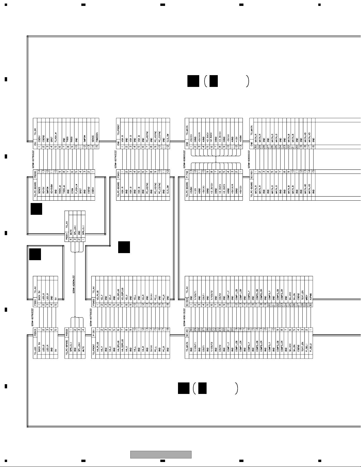
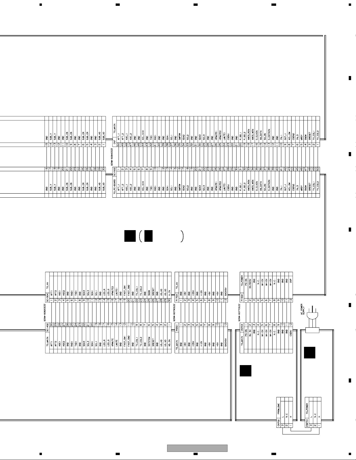
4. PCB CONNECTION DIAGRAM . . . . . . . . . . . . . . . . . . . . . . . . . . . . . . . . . . . . . . . 68
4.1 POWER and EMC UNITS . . . . . . . . . . . . . . . . . . . . . . . . . . . . . . . . . . . . . . . . 69
4.2 MAIN UNIT. . . . . . . . . . . . . . . . . . . . . . . . . . . . . . . . . . . . . . . . . . . . . . . . 70
4.3 FRONT, LED and SR CONNECT UNIT . . . . . . . . . . . . . . . . . . . . . . . . . . . . . . . . . 72
4.4 AV UNIT . . . . . . . . . . . . . . . . . . . . . . . . . . . . . . . . . . . . . . . . . . . . . . . . . 73
4.5 PC I/F UNIT . . . . . . . . . . . . . . . . . . . . . . . . . . . . . . . . . . . . . . . . . . . . . . . 74
5. PCB PARTS LIST . . . . . . . . . . . . . . . . . . . . . . . . . . . . . . . . . . . . . . . . . . . . . . 76
6. ADJUSTMENT . . . . . . . . . . . . . . . . . . . . . . . . . . . . . . . . . . . . . . . . . . . . . . . . 99
7. GENERAL INFORMATION. . . . . . . . . . . . . . . . . . . . . . . . . . . . . . . . . . . . . . . . . 105
7.1 DIAGNOSIS . . . . . . . . . . . . . . . . . . . . . . . . . . . . . . . . . . . . . . . . . . . . . . 105
7.1.1 TROUBLE SHOOTING . . . . . . . . . . . . . . . . . . . . . . . . . . . . . . . . . . . . . . . 105
7.1.2 DISASSEMBLY . . . . . . . . . . . . . . . . . . . . . . . . . . . . . . . . . . . . . . . . . . . 112
7.2 IC . . . . . . . . . . . . . . . . . . . . . . . . . . . . . . . . . . . . . . . . . . . . . . . . . . . 114
7.3 IC DESCRIPTIONS . . . . . . . . . . . . . . . . . . . . . . . . . . . . . . . . . . . . . . . . . . 138
8. PANEL FACILITIES . . . . . . . . . . . . . . . . . . . . . . . . . . . . . . . . . . . . . . . . . . . . 141
1234
4
1234
PDP-R03U
• accessories
Power cord Remote control unit
Two AA size batteries
(Alkaline batter
(QACCDA007WJPZ) (RRMCG1679CESA)
(TINS-7552CEZZ)(QCNW-6117CEZZ)
y)
System cable Operating instruction
Item
Media Receiver, Model: PDP-R03U
Reception System American TV standard NTSC system
TV
Function
Video signal detection PLL full synchr onous detection,
VHF/UHF
VHF 2–13ch, UHF 14–69ch
CATV
1–125ch
Audio multiplex
BTSC system
Terminals
S-VIDEO in, AV in, COMPONENT in
INPUT 2
S-VIDEO in, AV in
INPUT 3
S-VIDEO in, AV in, COMPONENT in, RGB in
Antenna
75 Ω UNBAL, F Type for VHF/UHF/CATV in
INPUT 4 S-VIDEO, AV in
PC
15 Pin mini D-Sub, Audio in
Monitor Out Terminal
S-VIDEO out, AV out, Audio (Variable, Fixed)
Power Requirement
120 V AC, 60 Hz, 40 W (0.2 W Standby)
Dimensions
420 (W) × 70 (H) × 330 (D) mm (16 9/16 (W) × 2 25/32 (H) × 13 (D) inch)
Weight
4.4 kg (9.7 lbs.)
Accessories
Power cord, Remote control unit, Two AA size batteries, System cable,
Operating instruction
Circuit type
Tuner
Rear
INPUT 1
Front
Rear
• Design and specifications ar e subject to change without notice.
Other Features
OSD Language
English/French/Spanish
Picture & Picture, Still image, Dual Tuner System
PLL digital synthesizer system
5678
1. SPECIFICATIONS
A
B
C
D
E
F
56
PDP-R03U
7
5
8
1234
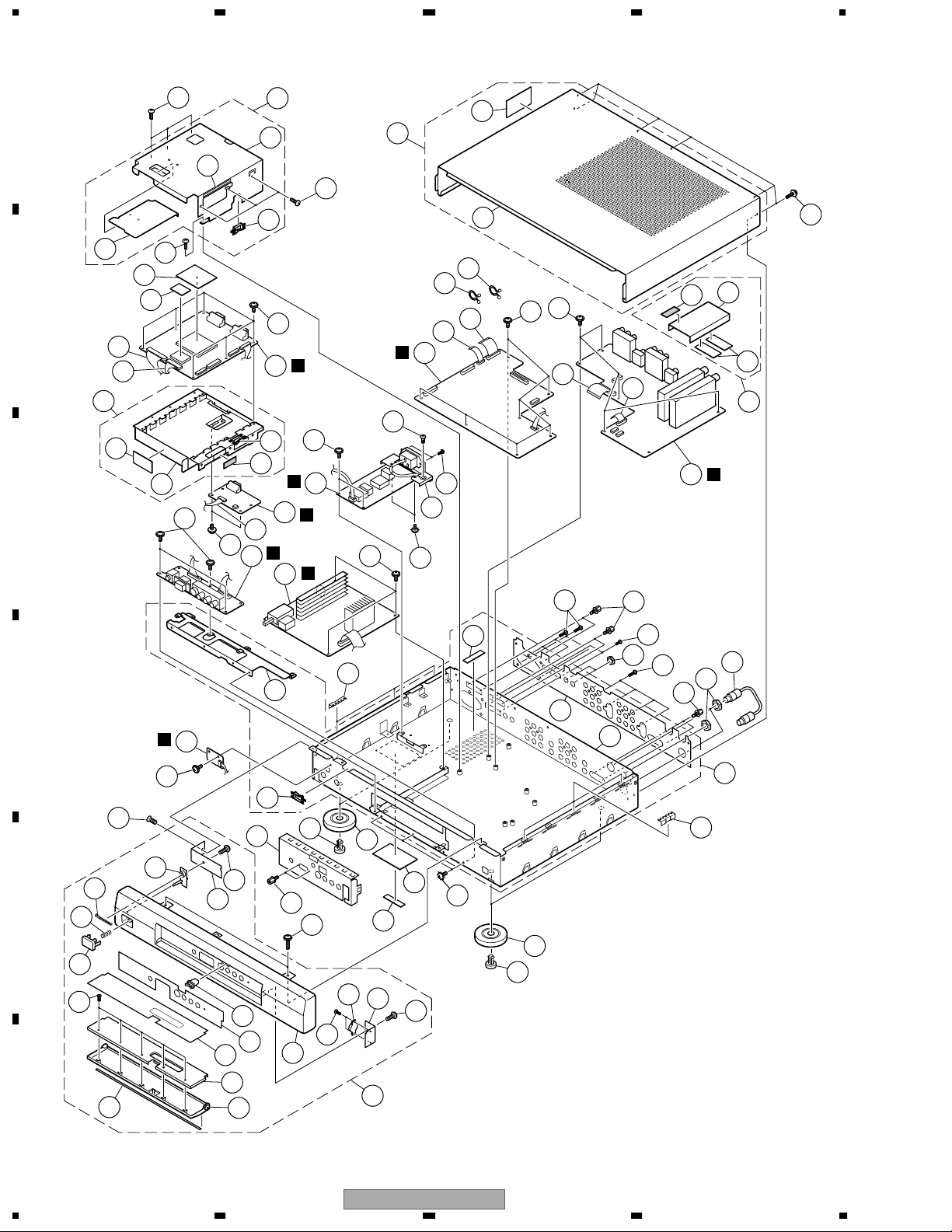
2. EXPLODED VIEWS AND PARTS LIST
NOTES:
A
2.1 PACKING
B
C
Parts marked by "NSP" are generally unavailable because they are not in our Master Spare Parts List.
The mark found on some component parts indicates the importance of the safety factor of the part.
Therefore, when replacing, be sure to use parts of identical designation.
Screws adjacent to mark on product are used for disassembly.
For the applying amount of lubricants or glue, follow the instructions in this manual.
(In the case of no amount instructions, apply as you think it appropriate.)
5. Operation Instructions
6. PDP Caution
2. System Cable
7. System Cable Caution
8. Caution Card
4. Batteries
1. Power Cord
3. Remote Control Unit
10. Packing Material
12. Polyethylene Bag
D
11. Buffer Material
11. Buffer Material
E
FRONT
9. Packing Case
13. No. Label
F
6
1234
PDP-R03U

>
5678
PACKING parts List
Mark
No. Description Part No.
1 Power Cord QACCDA007WJPZ
2 System Cable QCNW-6117CEZZ
3 Remote Control Unit RRMCG1679CESA
NSP 4 Battery (AA) • • • • • •
5 Operation Instructions TINS-7552CEZZ
(English/French/Spanish)
6 PDP Caution TCAUH1223CEZZ
7 System Cable Caution TCAUH1227CEZZ
8 Caution Card TCAUH1231CEZZ
9 Packing Case SPAKC5648CEZZ
10 Buffer Material SPAKXA001CEZZ
11 Packing Material SPAKF0515CEZZ
12 Polyethylene Bag SSAKH0173CEZZ
13 No Label TLABK0016CEZZ
A
B
C
D
E
F
PDP-R03U
56
7
8
7
1234
2.2 EXTERIOR SECTION
A
3-3
B
14
12
5
5-3
C
26
3-4
26
24
25
5-1
27
27
42
13
5-4
3-1
3-2
5-2
46
B
27
3
4
26
A
41
34
32
35
44
47
F
27
H
48
E
27
G
17
33
4-2
4-1
7
8
27
18
27
15
16
6-2
43
6-1
6-3
6
C
31
28
1-6
19
1-4
D
D
45
27
1-5
29
11
2-2
2-4
E
2-13
2-8
2-12
2-17
2-10
2-15
2-6
2-7
10
2-1
36
31
2-16
2-14
20
21
2-11
1-7
1-8
2-17
1-3
20
36
1-1
10
37
9
30
10
22
23
1
19
2-9
F
2-5
2-3
8
1234
2
PDP-R03U

5678
EXTERIOR SECTION parts List
Mark
No. Description Part No.
1 Bottom Cabinet Assy CCABA3103CE01
NSP 1-1 Bottom Cabinet • • • • • •
1-3 Terminal Indicator HINDP5928CESA
1-4 Fixing Metal LANGT9035CEFW
1-5 Holder LHLDW1021GE00
No. Description Part No.
Mark
12 Connecting Cord
13 Connecting Cord(SR-PC Boad) QCNW-6078CEZZ
14 Connecting Cord
15 FFC(Main-AV) QCNW-6081CEZZ
16 FFC(Main-AV) QCNW-6082CEZZ
(Front-PC Boad)
(main-PC Boad)
QCNW-6074CEZZ
QCNW-6080CEZZ
A
1-6 Gasket QEARZA007WJZZ
1-7 Model Label TLABM4302CEZZ
1-8 Screw XBPSD30P06R00
2 Front Panel Assy CWAKP1474CE01
NSP 2-1 Front Panel • • • • • •
2-2 LED Cover GCOVA2015CEKA
2-3 Door GDORF3026CEKA
2-4 Pioneer Badge HBDGE3130CESA
2-5 Decoration Plate HDECP0171CESA
2-6 Control Indicator HINDP5932CESA
2-7 Door Indicator HINDP5852CESA
2-8 Power Button JBTN-2073CEKA
2-9 Fixing Metal(Door) LANGF9655CESA
2-10 Fixing Metal LANGF9660CEFW
2-11 Fixing Metal(Damper) LANGT9040CEFW
2-12 Screw LX-HZ3111CEFN
2-13 Spring MSPRC0061CEFW
2-14 Damper PDMPF1009CEZZ
2-15 Ratch PKAI-0004GEZZ
2-16 Screw XBPSD20P05000
2-17 Screw XEBSD30P08000
3 Shield Assy CSLDM4688CE01
NSP 3-1 Shield • • • • • •
3-2 Holder LHLDW1021GE00
3-3 Heat Sink PRDAR1567CEFW
3-4 Spacer PSPAH0720CEZZ
4 Top Cabinet Assy CCABB3078CE01
NSP 4-1 Top Cabinet • • • • • •
4-2 Caution Label TCAUHA001WJZZ
17 FFC(Main-PB_BD)) QCNW-6083CEZZ
18 FFC(Main-PB_BD)) QCNW-6084CEZZ
19 Ground-Part(Cabi) QEARZ0056CEFW
20 Leg GLEGP9133CESA
21 Serial No. Label TLABN0411CEZZ
22 RF Cable QCNW-A342WJZZ
23 Nut,x3 LX-NZ3047GEZZ
24 Spacer PSPAZ0464CEKZ
25 Spacer PSPAZ0465CEKZ
26 Screw,x7 XBBSN30P06000
27 Screw,x30 XBPSD30P06JS0
28 Screw,x4 XBPSN30P06000
29 Screw XBSSD30P06000
30 Screw,x4 XEBSF30P08000
31 Screw,x8 XJPSN30P08XS0
32 AC Inlet Angle LANGK3000SNEZ
33 Screw, x2 XBSSF30P06000
34 Screw XBPBN40P06K00
35 Screw, x2 LX-BZ1001SNEZ
36 Screw,x4 LX-LZ1005AEZZ
37 Nut,x2 LX-NZ3182CEFN
38 • • • • • •
39 • • • • • •
40 • • • • • •
41 MAIN UNIT DUNTKA535DE04
42 FRONT UNIT DUNTKA617DE01
43 AV UNIT DUNTKA616DE01
44 SR CONNECT UNIT DUNTKA618DE01
45 LED UNIT DUNTKA619DE01
46 PC I/F UNIT CPCI-0056CE15
B
C
D
5 Fixing Metal Assy CANGT9033CE01
NSP 5-1 Fixing Metal • • • • • •
5-2 Holder LHLDW1021GE00
5-3 Shield PSLDM0152CEZZ
5-4 Spacer PSPAH0721CEZZ
6 Ground-Part Assy CANGTA001WJ01
NSP 6-1 Ground-Part • • • • • •
6-2 Spacer PMLT-A001WJZZ
6-3 Gasket QEARZA010WJZZ
7 Holder LHLDW1009CEZZ
8 Holder LHLDW1060CEZZ
9 Screw LX-BZ3434CEFN
10 Shaft NSFTZ0134CEFW
11 Shield PSLDM4686CEFW
56
47 POWER UNIT RDENC0331CEZZ
48 EMC UNIT RDENCA007WJZZ
SERVICE JIGS
Connector, 30-pin QCNW-6099CEZZ
(PC I/F-MAIN)
Connector, 50-pin QCNW-6100CEZZ
(PC I/F-MAIN)
Connector, 4-pin QCNW-6101CEZZ
(SR-AV)
Connector, 13-pin QCNW-6102CEZZ
(PC I/F-FRONT)
Connector, 12-pin QCNW-6103CEZZ
(PC I/F-MAIN)
PDP-R03U
7
E
F
9
8
1234
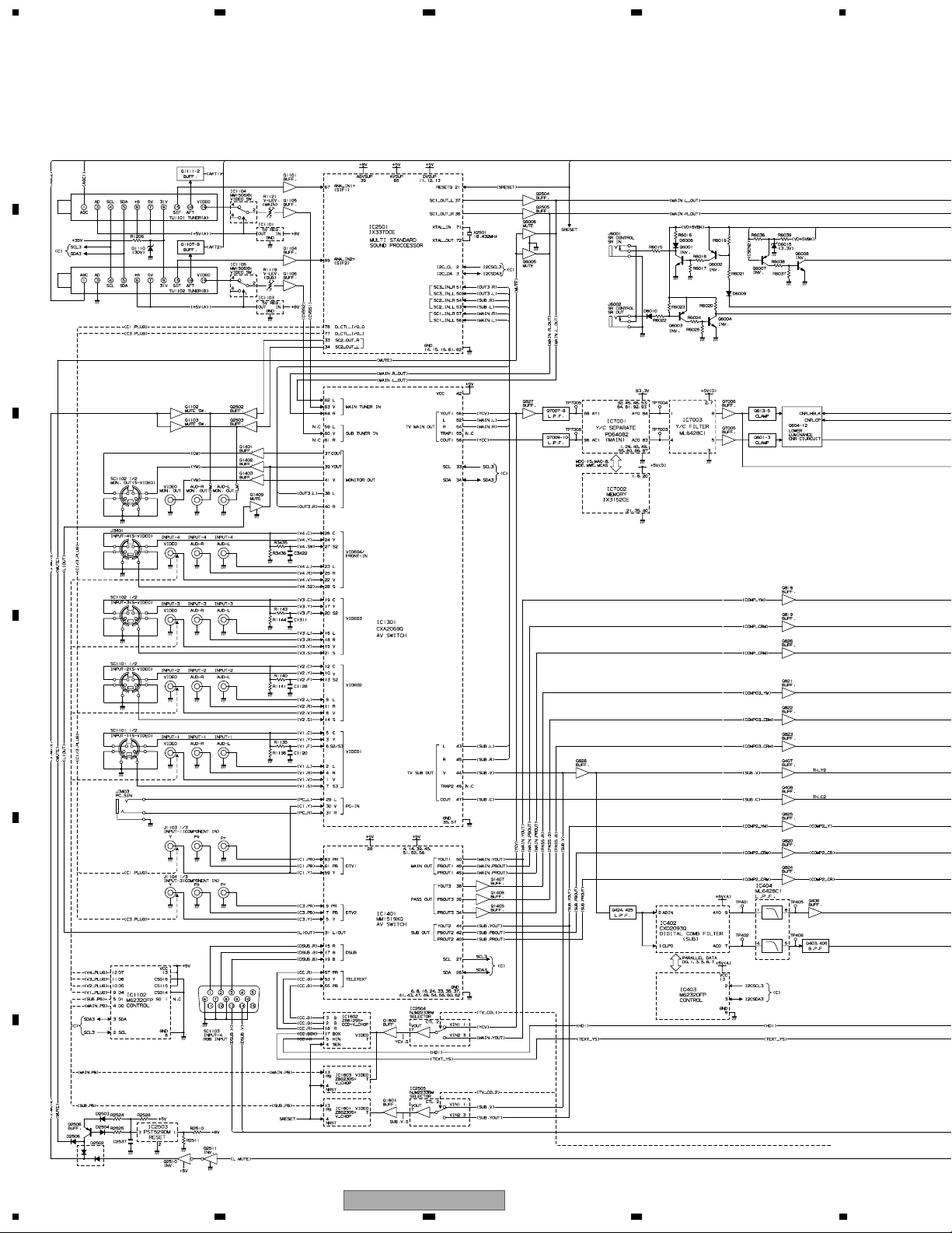
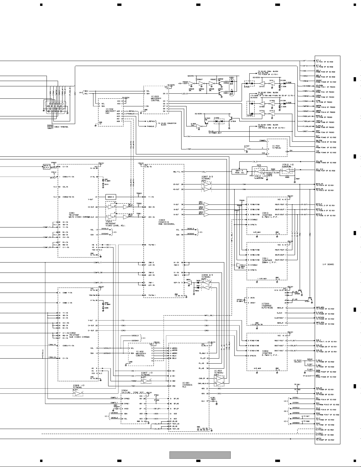
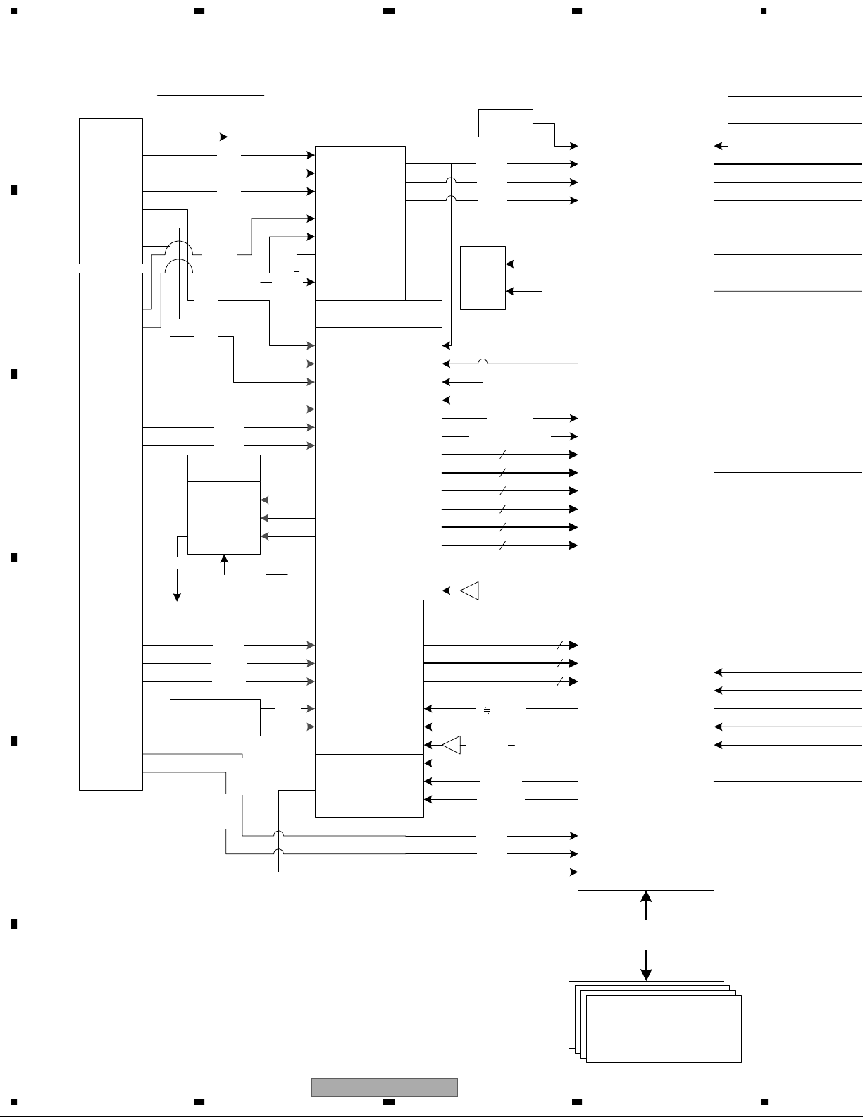
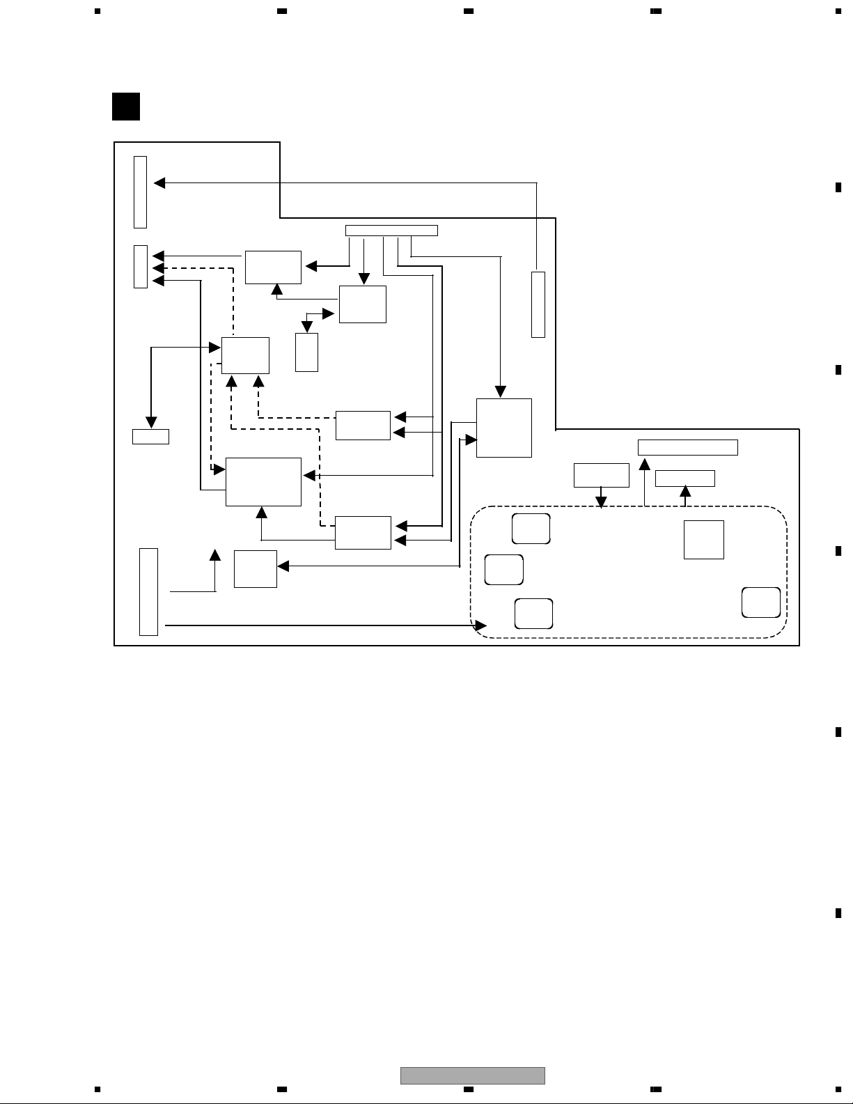
3. BLOCK DIAGRAM AND SCHEMATIC DIAGRAM
3.1 SYSTEM BLOCK DIAGRAM
A
ANT1
TU1101(C6h)
IN
OUT
ANT2
TU1102(C0h)
IN
VIDEO1
B
C
D
S
V
R
L
Y
Pb
Pr
VIDEO2
S
V
R
L
VIDEO3
S
V
R
L
Y
Pb
Pr
CH3
CH3
RGB
H/V
SIF
SIF
AV SWITCH
CXA2069Q(90h)
TV
R/L-TV
S1
V1
R/L1
S2 Y/VOUT1
V2 COUT1
R/L2 R/L 1
S3
V3 Y/VOUT 2
R/L3 COUT2
S4 R/L 2
V4
R/L4 Y/VOUT 3
V5 COUT3
R/L5 R/L 3
V6
R/L6
IC1301
IC1401
COMPONENT
AV SWITCH
MM1519XQ(94h)
YPbPrTV
YPbPr1 OUT1
YPbPr2 OUT2
YPbPr3 OUT3
LOUT1
C1-PLUG
C3-PLUG
CH3
CH
IC2501
SOUND
PROCESSOR
MSP3440(80h)
ANT1
ANT2 DACM
DACA
SC1
SC2 SC1
SC3 SC2
SC4
I/O1
I/O2
3
CH3
SRESET
P2502
SPR_CLI
SPL_DAI
IC2504
AnalogSW(MAIN)
NJM2233BM
IN1
IN2 OUT
CTL
IC2505
AnalogSW(SUB)
NJM2233BM
IN1
IN2 OUT
CTL
TO SR UNIT
(TO PDP)
IC1602
C.C
Z86129(28h)
VIDEO RGB
HD BOX
IC1603
V-CHIP(MAIN)
Z86230(2Ah)
VIDEO
IC1601
V-CHIP(SUB)
Z86230(28h)
VIDEO
IC7001
3D Y/C
uPD64082(B8H)
AYI AYO
ACI ACO
IC7002
FRAME MEMORY
4Mbit EDO
CH3
CH3
CH1
IC403
I/O EXPANDD
M62320(78h)
D0 MODE2
D1 DVss
D2
D3 DVss
D4
D5 APCN
D6 TRAP
D7 DVss
CH3
CH 3
MONITOR OUT
S
V
R
L
E
VIDEO4
S
V
R
L
PC
R/L
F
10
Y MUTE
IC1102
I/O EXPANDD
62320(74h)M
D1
D2
D3
D4 V1PLUG
D5 V2PLUG
D6 V3PLUG
D7 V4PLUG
PDP-R03U
CH3
L MUTE
POWER LED CONTROL
from TUNER
ABL
It is destination distinction at H/L of 2bit.
It goes into process mode by dropping on GND.
IC1503
DI/O EXPAND
M62320(74h)
D0 IN1
D1 LED-R
D2 D_POW
D3 +2.5POW
D4 IN3
D5 LED-G
D6 DACRST
D7 SMPOW
CH1
SC1502
AFT-1/ 2
AGC-1/2
ACL_SIG
I2C-CH1
I2C-CH2
I2C-CH3
SMPOW
L-MUTE
PSEL-1/2
TBUS
IN1
IN3
OUT1
ACL-SW
MRDY
SRESET
TV-COL1
TV-COL2
or
1234
LOWER LUMINANCE CNR
IC402
3Line COM
CXD2093Q
ADIN AYO
ACO
5678
A
CH3
IC801
SIG. PROCESSO R
(MAIN)
TB1274AF(88h)
CVBS/Y1 YOUT
C1
CVBS/Y2 CbOUT
C2
CVBS/Y3 CrOUT
C3 H/V
YS2/YM
YCbCr1
YCbCr2
RGB1
RGB2
IC802
SIG. PROCESSO R
(SUB )
TB1274AF(8Ah)
CVBS/Y1
C1 YOUT
CVBS/Y2 CbOUT
C2 CrOUT
CVBS/Y3
C3 H/V
COMB_Y
COMB_C
YCbCr1
RGB1
RGB2
CH3
LEVEL ADJ.
LEVEL ADJ.
CB-GAIN
CR-MAIN
SIG. PROCESSO R
CXA2101Q(84h)
YCbCr1
H/V1
YCbCr2
H/V2 ROU T
YCbCr3 GOUT
H/V3 BOU T
YCbCr4
H/V4
YCbCr5 H/V
H/V5
YS/YM1
RGB1
RGB2
SCP
ABL FIL
H-BLK GEN. PLD
EPM3064-10
SP_H/V/CLP PL_H/V
HD/VD1 PL_BLK/CLP
HD/VD2 HD/VD3
US_H/V CNR_CLP/BLK
AW_VBLK TEXT_H/V
HDS/VDS
IC803
IC1901
CH3
LPF6.7M(MAIN)
ML6426-1
RGB INA
RGB INB RGB
A/B MUX
SYNC
IC811
LPF30M(MAIN)
ML6426-1
RGB INA
RGB INB RGB
A/B MUX
SYNC
IC804
LPF6.7M(SUB)
ML6426-1
RGB INA
RGB INB RGB
A/B MUX
SYNC
IC810
SC1501
MAIN R
MAIN G
MAIN B
MAIN H
MAIN V
SUB Y
SUB Cb
SUB Cr
SUB H
SUB V
B
PC I/F UNIT
C
PC I/F UNIT
IC15
DAC EXPAN D
M62393(92h)
A1 CR-MAIN
A2 CR-SUB
A3 +B2.5
A4 +BADJ2
A5 REFADJ
A6
A7
A8 CB-GAIN
RESET
IC7200
V-BLK GEN. AutoWide
IX-3289CE
Y/V IN VBLK
H/ V
CH
1
IC1504
AnalogSW
TC7W53
IN0 OUT
IN1
CNT
IC1708
REG
+5V(A )
IC1710
REG
+5V(A )
IC1711
REG
+5V(D )
IC1712
REG
+5V(A
IC1902
I/O EXPAND
M62320(7Bh)
D0 MODEC
D1 MODEB
D2 MODEA
D3 SEL_A
D4 SEL_OE
D5 MFIL_SEL
D6
D7
SYNC. SEP.
TA1318(D8h)
HD/VD1
HD/VD2 HD/VD 1
HD/VD3 HD/VD 2
SYNC1 CP
SYNC2
REG
+8V
REG
+9V(A
)
IC604
IC1706
IC1704
CH3
D
CH3
POWER UNIT
P1502
PS-ON
T1701
DC/DC
B35V
D6V
-5 V
+12VA
+5VBK
+10V
+2.5POW
IC1709
REG
+5V(A)
IC1713
REG
+12V
P1702
+5 VBK
+12V
-5V(A)
+3.3V(D)
+2.5VCV
+5V(A)
+5V(D)
P3401
RGB H/V
CLR-SW
E
PC I/F UNIT
PC I/F UNTI
F
BACK UP
IC1701
DC/DC
+2.5VCV
+3.3V(D)
)
+6V
PDP-R03U
56
7
8
11
1234
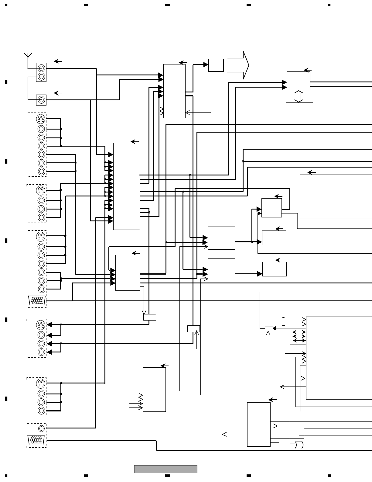
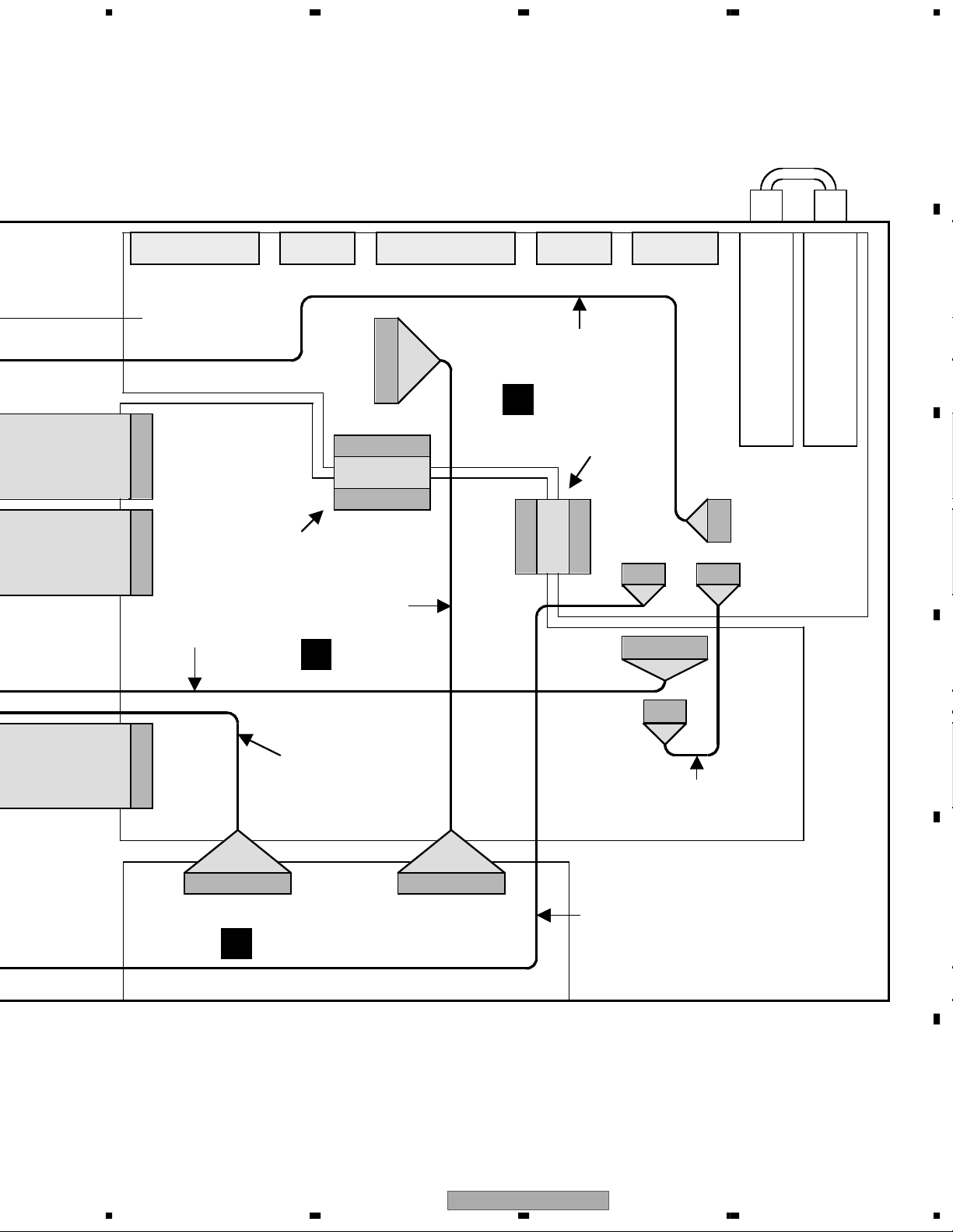
3.2 SIGNAL FLOW BLOCK DIAGRAM
A
B
C
D
E
F
12
1234
PDP-R03U
5678
A
B
C
D
E
PDP-R03U
56
F
13
7
8
1234
3.3 DC/DC CONVERTER CONNECTION DIAGRAM
A
B
C
D
E
F
14
1234
PDP-R03U
5678
A
B
C
D
E
PDP-R03U
56
F
15
7
8
1234
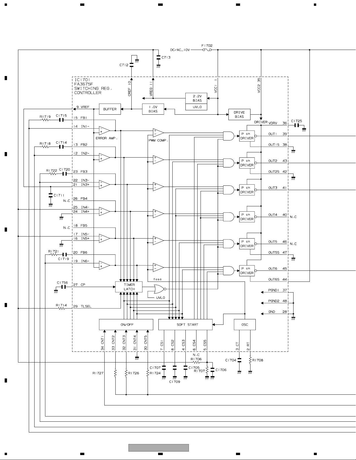
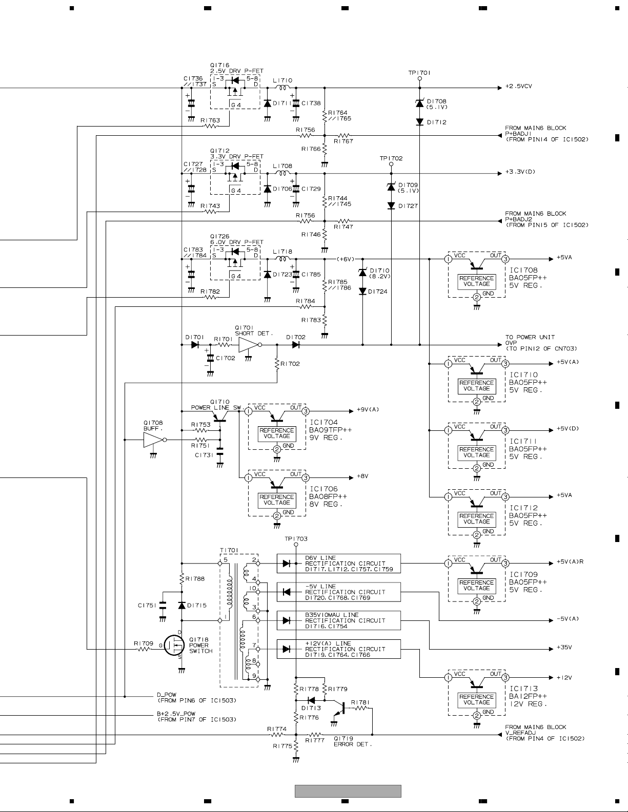
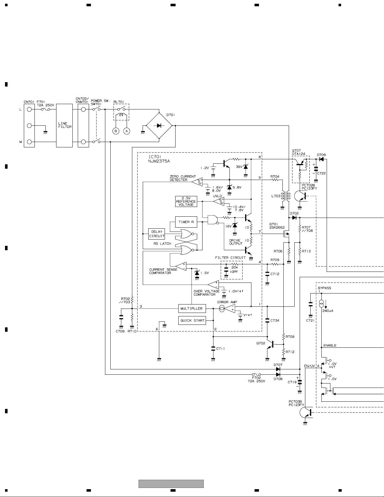
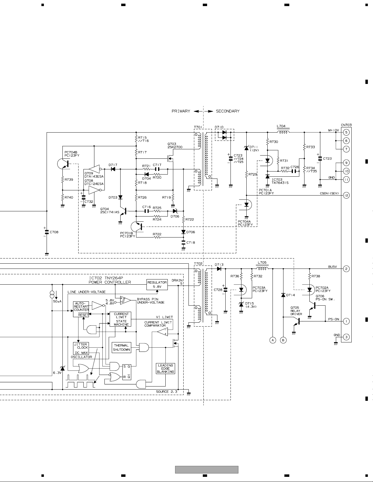
3.4 POWER BLOCK DIAGRAM
A
B
C
D
E
F
16
1234
PDP-R03U
5678
A
B
C
D
E
PDP-R03U
56
F
17
7
8
1234
3.5 PC/IF BLOCK DIAGRAM
A
CPCI-00 56CE
X4
CLR_ SW
12
7
9
10
CN8
5
1
3
12pin TO CONNECTOR PWB
B
18
17
29,3
0
25,2
21,2
6
2
FPC 30pin TO MAIN PWB
C
PC _H
PC_V
PC_C
MAIN _H
D
MAIN_VD
PC_R
PC _G
PC_B
MAI N_
R
MAI N_
G
MAI N_
B
12V->9V R eg
IC415 BA09FP
HV SEL
VIDEO SIGNAL
PEAK DETECTION
CN6
ACL_S IG
OV0_CLP
1B
2B
4B
1A
2A
4A
-A /+B
RIN2
GIN2
BIN2
RIN1
GIN1
BIN1
ROUT
GOUT
BOUT
74LCX157
1Y
2Y
V0
4Y
Sync
Sel
IC411
12V->5VReg
IC7 PQ05TZ11
V0
A/D
Amp
PLL
IC4
CXA3506R
2
C=CH2
I
XPOWERSAVE
SYNCIN1
SYNCIN2
HOLD
CLPIN
DIVOUT
1/2C LK
RA[7..0]
RB[7..0]
GA[7..0]
GB[7..0]
BA[7..0]
BB[7. .0]
25MHz
OV0 _H
OV0_V
PC_ C3
CXA3506R
VCO
WHISKER
CORRECTIO
N CIRCUIT
IC423, IC424
OV0_CLP
OV0_HSC2
OVCLK(Max60MHz)
8
8
8
8
8
8
XPW R_SV
OV0_PDEN
OV0_HSYNR
V0_HSYNC
V0_VSYNC
V0_CSYNC
V0_PDEN
V0_HSYNR
V0_CLP
V0_HSYNC2
V0_VDCLK_I
V0_RA[7..0]
V0_RB[7..0]
V0_GA[7..0]
V0_GB[7..0]
V0_BA[7..0]
V0_BB[7..0]
CVIC
IC25
DCLKMCK_REF
DO_RA[9..2]
DO_GA[9..2]
DO_BA[9..2]
LCLK
DO_HSYNC
DO_VSYNC
DO_HDISP
BINT
5V->3.3V Reg
IC8 PQ20VZ11
13,1
D
4
9,10
5,6
2
1
SUB _Y
SUB_ Cb
SUB_ Cr
V1 ADC
RT, RB SETTING
CIRCUIT
SUB_ HD
3.27V
1.17V
About 60MHz
AIN
BIN
CIN
RT
RB
VCOOUT
V1
A/D
IC310
TLC5733A
V1
PLL
IC328
AO[8..1]
BO[8..1]
CO[8..1]
CLK
EXTCLP
-OE
FIN-A
FIN-B
PFDINH
OV1_VCKO
( 15M Hz)
OV1_CLP
SAD C_OE
OV1_HSNR
OV1_HSNF
OV1_PDEN
8
8
8
V1_GA[7..0]
V1_BA[7..0]
V1_RA[7..0]
V1_VDCLK_O
V1_CLP
V1_HSYNR
V1_HSYNF
V1_PDEN
BCLK
XBCS
BWAIT
XRESET
PLL_S
BD,BA
TLC2933IPW
E
SUB _VD
OV1 _H
OV1_V
OV1_VCLK
V1_HSYNC
V1_VSYNC
V1_VDCLK_I
SDRAM BUS
D:128,A:11,BA:2,Ctrl:13
SDCLK=100MHz
SDRAM
F
512Kx128bitx4 BANK
IC319-322
HY57V653220BTC-7 4 PCS.
18
PDP-R03U
1234
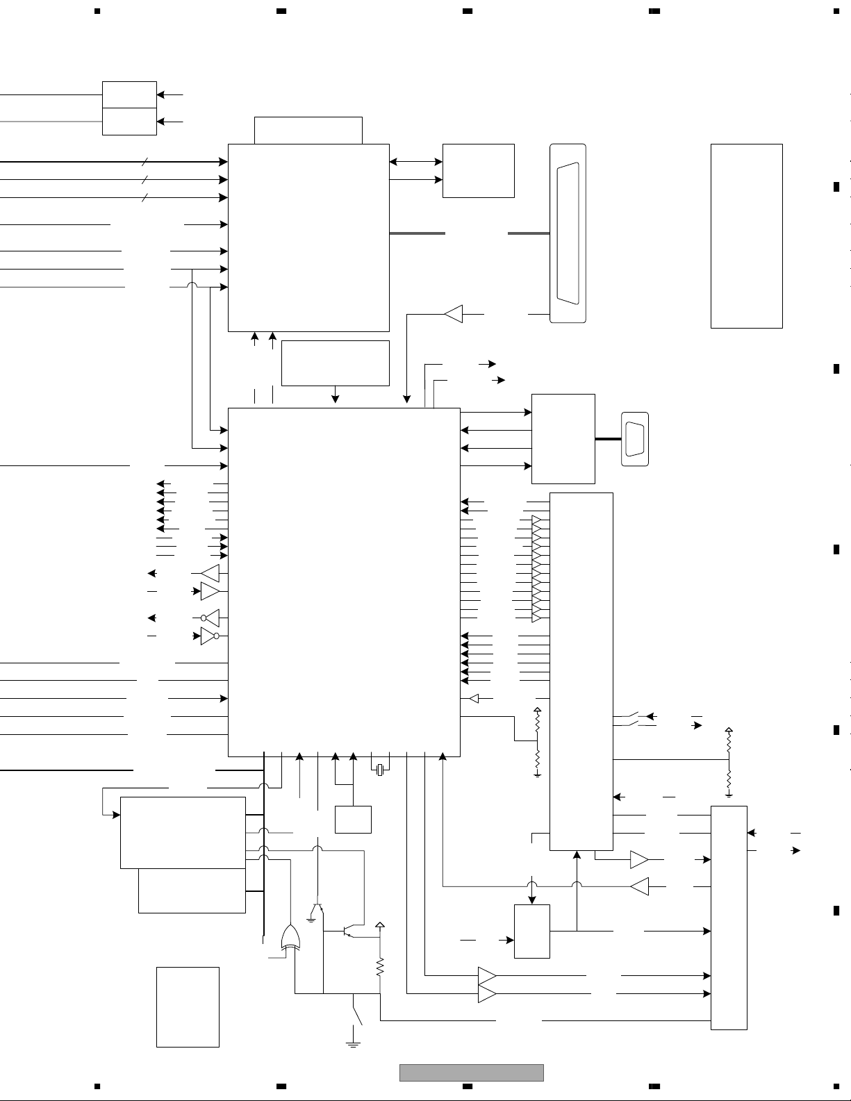
5678
X6
25.175MHz
X5
79.794MHz
8
8
8
LCLK(79.79 4MHz)
DO_HS YNC
DO_VS YNC
DO_HD ISP
-C1_I NT
CKIO(24MHz)
-CS2
-WAIT _C1
-RESET_C1
-
RST_P LL
CPU BUS D:16,A:26
WP
LH28F320S3NS
VGA_OE
WXGA_OE
XPWR_SV
HVSEL PTA0
SEL _CD
SAD C_OE
CAR D_RST
PXOE
THER MO
B SREQ
CLR_ SW PTD4
TXD 1_T
RXD 1_T
TXD0_M
RXD0_M
FLAS HWP
FLASH
2Mx16bit
IC27
-C S0
DRAM 1Mx16bit
IC28
MSM51V18165D
EEPROM
IC3
AT24C128N
2
C=CH3
I
D[23..16]
D[15..8]
D[7..0]
IDCK+
HSYNC
VSYNC
DE
IRQ3
IRQ4
IRQ0
PTC5
PTD7
PTE6
PTB7
PTC7
AN7
PTE6
TXD1
RXD1
TXD0
RXD0
CKIO
CS2
WAIT
PTD2
PTD5
STS
VPP
A20
5V->3.3V R eg
IC412 PQ1R33
PanelLink
HDCP
Transmitter
IC413
SiI168
2
C=CH1
I
EDGE
RST
RESET CIRCUIT
+2.5V IC19 PST623XW
+3.3V IC2 PST600IW
-RST _PL
MON_DET
PTB3
PTA1
INTERNAL 72MHz
EXTERNAL 24MHz
CH1 Do:PTB4,Di:PTG5,Clk:PTB5
CH2 Do:PTC1,Di:PTF2,Clk:PTC2
CH3 Do:PTA6,Di:PTG6,Clk:PTA7
CH4 Do:PTD0,Di:PTG4,Clk:PTA4
D[15..0],A[25..0]
PTD1
PTF0
FST ATUS
A20
RESETP
CPU
IC1
SH7709
I2C PORT
SCK1
PTE1
1.8432MHz
FLWP
S1
X3
EEPROM
IC414
M24C32
TMDS(4ch)
VGA_ OE
WXGA_OE
CE2A
CKE
TXD2
RXD2
CTS2
RTS2
IRQ1 4
PTJ4
DAC_DATA
DAC_CLK
RES_OUT3
PTE1 3
SRESET
PTC4 1
TV_COL2
PTC0 2
TV_COL1
PTB2 26
HPMUTE
PTB0 24
PTJ7 14
PTA5 18
PTA3 17
PTG1 15
PTC6
PTE7
LMUTE
SH_ON
AWC S_R
AWC S_W
AN1 47
AN4
AN3
AN6
AN5
AN2
CVIC INTERNAL SUPPLY VOLTAGE
MONITOR
R1105 MOUNTED: VD+2.5V=2.5V
R1106 MOUNTED: VD+2.5V=1.8V
PC_V
SCK2
MDA
MCK
TX
EXTAL
X1
6 MHz
PTD6
XTAL
PTB6
FLASH WRITE AT FWMODEN=LOW
HOTPLUG
SSYSTEM
KOUTEI
ACL_SW
1
AG C1
AG C2
AF T1
AF T2
PSE L1
PSE L2
AW_ DATA
uPD4721G
R1105R1106
IO_STB
PC
DDC
DETECT
16
RS232C
Driver&
Reciever
IC405
5PTG2
13
16PTJ5
8PTE3
25PTE2
48AN0
50
49
20
19
10
CN3
DVI
I2C=CH1
(TO MONITOR)
RS232C
SERIAL=CH2
FPC 50pin (TO MAIN PWB)
I2C=CH1,2,3, SERIAL=CH1
CN7
SERIAL CONNECTION FOR
CE01 ONLY
(R1081, R1080)
42
41
6
9
7
23
FLASH_W
SRST 4
ACL_S IG44
CSEN2
TXD 1_T
RXD 1_T
SENCE
SMPOW
1:VD+5
3:VA+5
5,6:VD+2.5
8:VD+3.3
10:V-5
12:VA+12
13:VD+5BK
CN5
CVIC INTERNAL SUPPLY
VOLTAGE SELECTOR
R1077 MOUNTED: VD+2.5V=2.5V
R1078 MOUNTED: VD+2.5V=1.8V
R1077R1078
14
1235
1CSEN1
6CCKM
CN1
2
5
15pin
15FWMODEN
CN9
13pin (TO MAIN PWB)
POWER CONNECTOR
8
TXD 1_T
9
RXD 1_T
SERIAL=CH0
A
B
C
D
E
F
PDP-R03U
56
7
8
19
1234
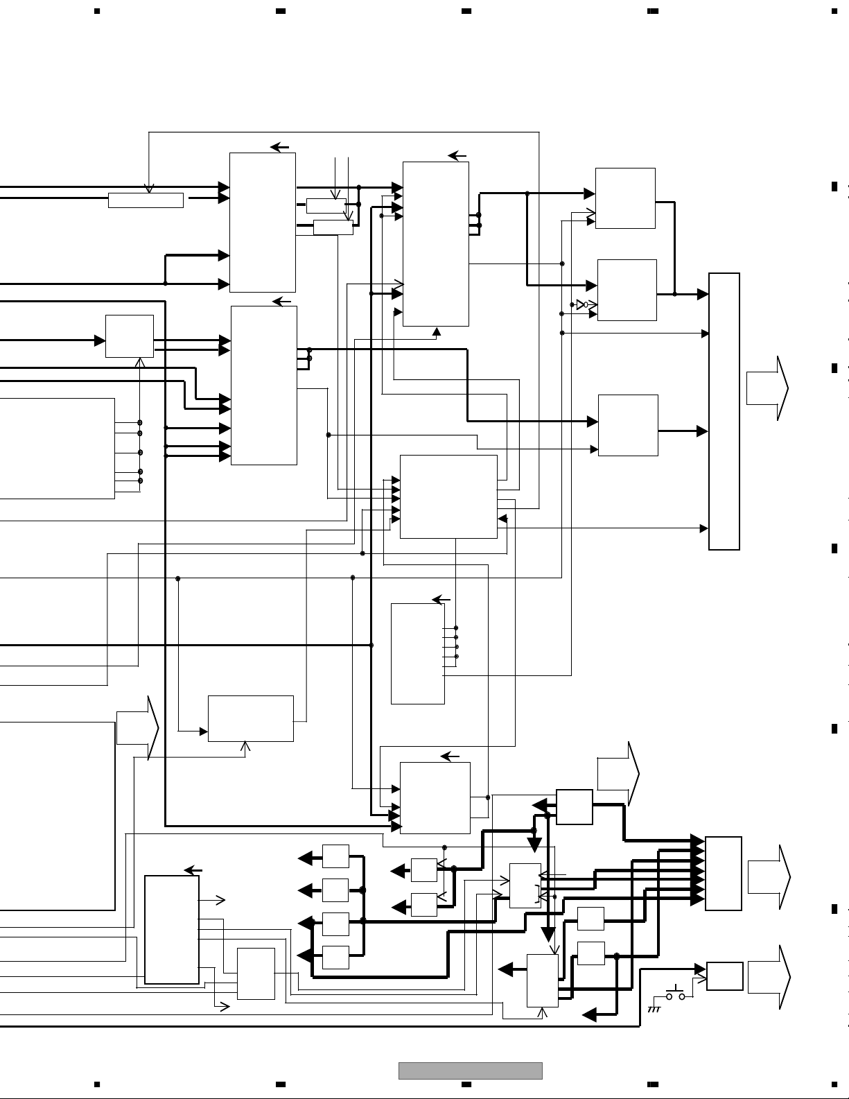
3.6 PRINTED WIRING BOARD BLOCK DIAGRAM
A
PC/IF UNIT
F
VIDEO PROCESSOR
CIRCUIT
POWER REG.
CIRCUIT
IC25
CIVIC
IC319
SDRAM
IC320
SDRAM
PC R,G,B INPUT
CIRCUIT
CN9
CONNECTOR
IC7
REG.
IC8
REG.
B
IC4
VIDEO MAIN/PC
A/D CONV
CN8
CONNECTOR
VIDEO IN A/D
CONVERTER
CIRCUIT
IC310
VIDEO SUB
A/D CONV
IC1
CPU
CPCI-0056CE
IC413
PANEL LINK
IC405
RS-323 RECIVER
CN3
DISPLAY OUT-1
CN5
RS-232C
PANEL LINK
OUTPUT
CIRCUIT
RS-232C LINE
DRIVER I/F
CIRCUIT
C
CN6
CONNECTOR
CN
CONNECTOR
CN1
CONNECTOR
CPU CIRCUIT
AV UNIT
C
J1103
INPUT1 AV TERMINAL
D
INPUT2 AV TERMINAL
INPUT1 CONPONENT TERMINAL
IC1401
AV SWITCH
IC1102
CONTROL
SC1101
INPUT1, INPUT2
S-VIDEO TERMINAL
P1301
CONNECTOR
E
SC1401
COMP. AV SWITCH CIRCUIT
CONNECTOR
ANALOG AV SWITCH CIRCUIT
F
J1104
INPUT3 AV TERMINAL
INPUT3 CONPONENT TERMINAL
MONITER OUT AV TERMINAL
IC1301
AV SWITCH
SC1102
INPUT3, MONITER OUT
S-VIDEO TERMINAL
SC1402
CONNECTOR
P2503
CONNECTOR
IC1602
CCD
IC1601
V-CHIP
IC1603
V-CHIP
P2502
CONNECTOR
P2501
CONNECTOR
SC1103
INPUT4
RGB TERMINAL
TU1102 U/V TUNER
IC2501
MULTI SOUND
TU1101 U/V TUNER
V-CHIP CIRCUIT
20
PDP-R03U
1234
5678
MAIN UNIT
A
SC1502
CONNECTOR
SC1501
CONNECTOR
P1901
PROGRAMMING
CONNECTOR
P1502
CONNECTOR
IC802
SUB VIDEO CHROMA
IC1901
PLD
IC803
RGB DECODER
IC402
SUB COMB FILTER
IC403
CONTROL
IC604
SYNC SEPARATE
IC801
MAIN VIDEO CHROMA
SC1503
CONNECTOR
IC7001
Y/C SEPARATE
L1708
SC1504
CONNECTOR
IC1502
DAC
A
B
P1702
CONNECTOR
C
P1703
CONNECTOR
T1701
POWER SUPPLY
IC7002
MEMORY
L1718
DC/DC CONVERTER CIRCUIT
L1710
L1711
D
E
PDP-R03U
56
F
21
7
8
1234
A
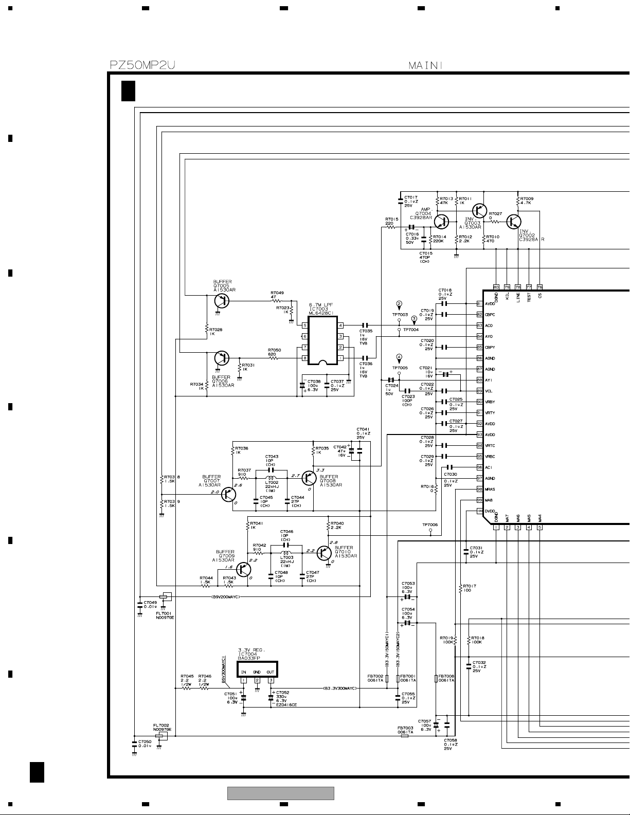
DESCRIPTION OF SCHEMATIC DIAGRAM
VOLTAGE MEASUREMENT CONDITION:
1. When the exclusive-use AC adapter is used, the color
bar signal of color bar generator for service is input to
get the normal screen. When the audio is minimized,
the voltage value is measured with the 20 k /V tester.
WAVEFORM MEASUREMENT CONDITION:
B
1. When the exclusive-use AC adapter is used, the color
density, lightness and color hue are set to the center
position, and the signal of color bar generator for service
is observed to get waveform.
2. indicates waveform check points (See chart,
waveforms are measured from point indicated to
chassis ground.)
INDICATION OF RESISTOR & CAPACITOR:
C
RESISTOR
1. The unit of resistance “” is omitted.
(K=k =1000 , M=M ).
2. All resistors are ± 5%, unless otherwise noted.
(J= ± 5%, F= ± 1%, D= ± 0.5%)
3. All resistors are Carbon type, unless otherwise noted.
C : Solid W : Cement
S : Oxide Film T : Special
N : Metal Coating
CAPACITOR
1. All capacitors are mF, unless otherwise noted.
(P=pF=mmF).
2. All capacitors are Ceramic type, unless otherwise
noted.
(ML) : Mylar (TA) : Tantalum
(PF) : Polypro Film (ST) : Styrol
CAUTION:
This circuit diagram is original one, therefore there may be a
slight difference from yours.
IMPORTANT SAFETY NOTICE:
PARTS MARKED WITH “ ” ( )ARE
IMPORTANT FOR MAINTAINING THE SAFETY OF
THE SET. BE SURE TO REPLACE THESE PARTS
WITH SPECIFIED ONES FOR MAINTAINING THE
SAFETY AND PERFORMANCE OF THE SET.
D
E
F
22
PDP-R03U
1234
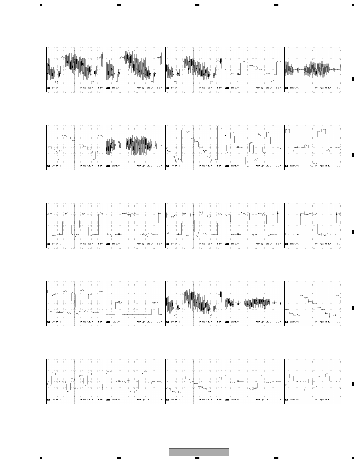
WAVEFORMS
1
IC1301 63-pin
V: 200mV/div H: 10µsec/div
2
IC1301 60-pin
V: 200mV/div H: 10µsec/div
3
IC1301 56-pin
V: 500mV/div H: 10µsec/div
4
TP7004
V: 200mV/div H: 10µsec/div
5
TP7003
V: 200mV/div H: 10µsec/div
6
TP812
V: 200mV/div H: 10µsec/div
7
TP603
V: 200mV/div H: 10µsec/div
8
TP803
V: 100mV/div H: 10µsec/div
9
TP802
V: 100mV/div H: 10µsec/div
0
TP801
V: 100mV/div H: 10µsec/div
-
TP809
V: 200mV/div H: 10µsec/div
=
TP808
V: 200mV/div H: 10µsec/div
~
TP807
V: 200mV/div H: 10µsec/div
!
IC810 13-pin
V: 200mV/div H: 10µsec/div
@
IC810 11-pin
V: 200mV/div H: 10µsec/div
#
IC810 10-pin
V: 200mV/div H: 10µsec/div
$
IC803 31-pin
V: 1V/div H: 10µsec/div
%
IC1301 44-pin
V: 500mV/div H: 10µsec/div
^
TP410
V: 500mV/div H: 10µsec/div
&
IC802 21-pin
V: 200mV/div H: 10µsec/div
*
IC802 22-pin
V: 200mV/div H: 10µsec/div
(
IC802 23-pin
V: 200mV/div H: 10µsec/div
)
IC804 13-pin
V: 500mV/div H: 10µsec/div
_
IC804 11-pin
V: 500mV/div H: 10µsec/div
+
IC804 10-pin
V: 500mV/div H: 10µsec/div
5678
A
B
C
D
56
PDP-R03U
7
E
F
23
8
1234
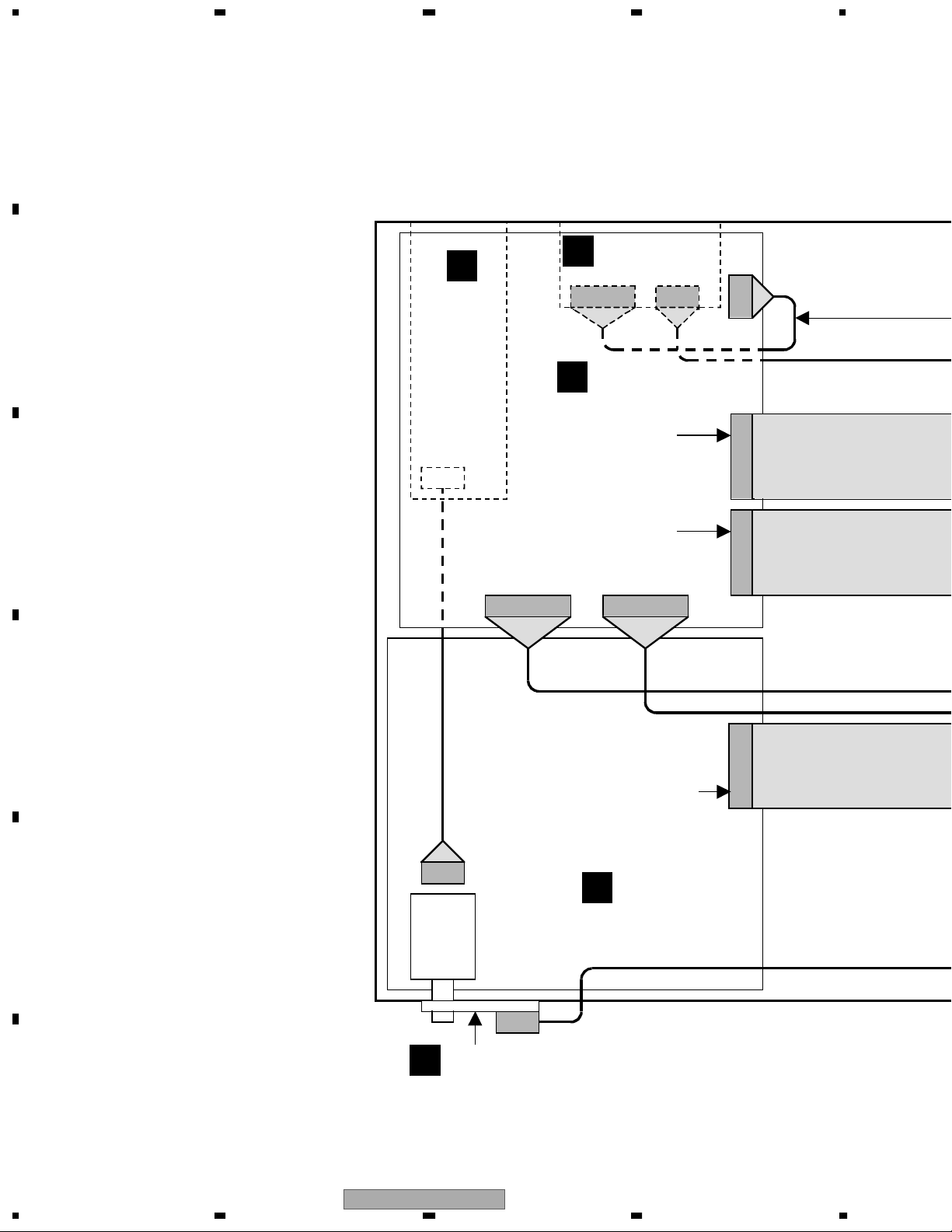
3.7 OVERALL WIRING DIAGRAM (1)
A
B
H
EMC
UNIT
SR CONNECT
E
UNIT
P6000 P6001
F
PC I/F UNIT
QCNW6084CEZZ
CN1
CN7
C
CN9 CN8
D
CN702
QCNW6083CEZZ
CN6
CN703
QCNW-6077CEZZ
G
E
POWER UNIT
P3001
LED UNIT
D
F
24
1234
PDP-R03U
5678
Note : When ordering service parts, be sure to refer to "EXPLODED VIEWS and PARTS LIST" or "PCB PARTS LIST".
QCNW-6078CEZZ
QCNW-A280WJZZ
TUNER
TUNER
P1301
AV UNIT
C
SC1401
QCNW-6082CEZZ
SC1502
P2502
P2501
SC1501
SC1503
QCNW-6081CEZZ
SC1504
P2503
SC1402
A
B
C
QCNW-6073CEZZ
QCNW-6080CEZZ
P1502
QCNW-6074CEZZ
P3401 P3402
FRONT UNIT
B
MAIN UNIT
A
P1702
P1703
QCNW-6079CEZZ
QCNW-6076CEZZ
D
E
PDP-R03U
56
F
7
25
8
1234
3.8 OVERALL WIRING DIAGRAM (2)
A
F
PC I/F UNIT (CPCI-0056CE15)
B
C
SR CONNECT
E
UNIT
(DUNTKA
618DE01)
LED
D
UNIT
(DUNTKA
D
619DE01)
B
FRONT UNIT
(DUNTKA617DE01)
F 1/7-7/7
E
C
AV UNIT (DUNTKA616DE01)
F
26
1234
PDP-R03U
C 1/3-3/3
5678
A
B
A
A 1/7-7/7
MAIN UNIT (DUNTKA535DE04)
G
POWER UNIT
(RDENC0331CEZZ)
C
D
E
H
EMC
UNIT
(RDENCA
007WJZZ)
PDP-R03U
56
F
7
27
8
1234
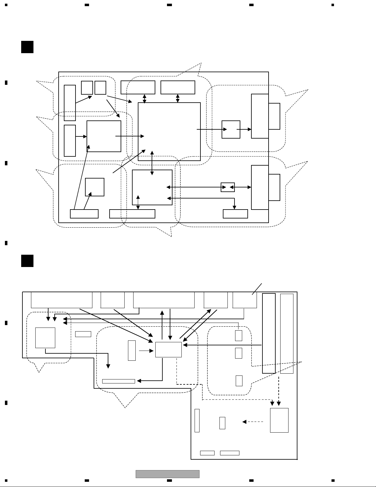
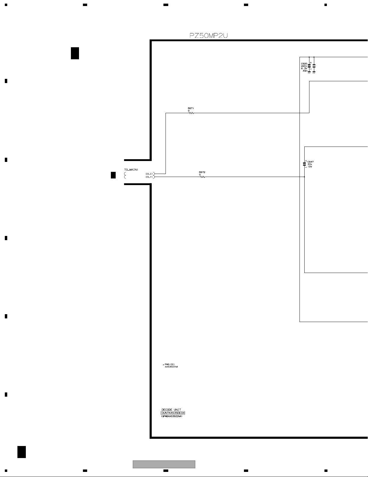
3.9 MAIN UNIT (1/7)
A
A 1/7
B
C
MAIN UNIT (DUNTKA535DE04)
D
E
F
A
A
28
1/7
PDP-R03U
1234
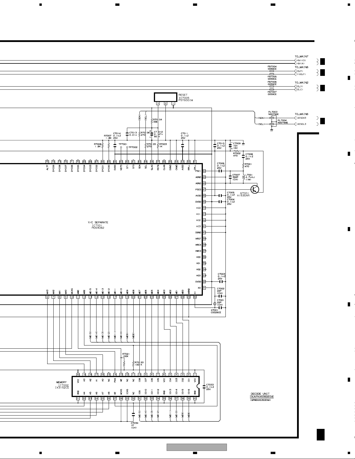
5678
A
A
7/7
A
6/7
A
2/7
B
A
6/7
C
D
E
PDP-R03U
56
F
A
1/7
7
29
8
1234
3.10 MAIN UNIT (2/7)
A
B
A 2/7
MAIN UNIT
(DUNTKA535DE04)
A
1/7
C
D
E
F
A
2/7
A
30
1234
PDP-R03U
 Loading...